EP3875202A1 - Power source device for electric discharge machine - Google Patents
Power source device for electric discharge machine Download PDFInfo
- Publication number
- EP3875202A1 EP3875202A1 EP18938322.7A EP18938322A EP3875202A1 EP 3875202 A1 EP3875202 A1 EP 3875202A1 EP 18938322 A EP18938322 A EP 18938322A EP 3875202 A1 EP3875202 A1 EP 3875202A1
- Authority
- EP
- European Patent Office
- Prior art keywords
- current
- value
- power supply
- switching elements
- period
- Prior art date
- Legal status (The legal status is an assumption and is not a legal conclusion. Google has not performed a legal analysis and makes no representation as to the accuracy of the status listed.)
- Pending
Links
Images



Classifications
-
- B—PERFORMING OPERATIONS; TRANSPORTING
- B23—MACHINE TOOLS; METAL-WORKING NOT OTHERWISE PROVIDED FOR
- B23H—WORKING OF METAL BY THE ACTION OF A HIGH CONCENTRATION OF ELECTRIC CURRENT ON A WORKPIECE USING AN ELECTRODE WHICH TAKES THE PLACE OF A TOOL; SUCH WORKING COMBINED WITH OTHER FORMS OF WORKING OF METAL
- B23H1/00—Electrical discharge machining, i.e. removing metal with a series of rapidly recurring electrical discharges between an electrode and a workpiece in the presence of a fluid dielectric
- B23H1/02—Electric circuits specially adapted therefor, e.g. power supply, control, preventing short circuits or other abnormal discharges
- B23H1/022—Electric circuits specially adapted therefor, e.g. power supply, control, preventing short circuits or other abnormal discharges for shaping the discharge pulse train
-
- B—PERFORMING OPERATIONS; TRANSPORTING
- B23—MACHINE TOOLS; METAL-WORKING NOT OTHERWISE PROVIDED FOR
- B23H—WORKING OF METAL BY THE ACTION OF A HIGH CONCENTRATION OF ELECTRIC CURRENT ON A WORKPIECE USING AN ELECTRODE WHICH TAKES THE PLACE OF A TOOL; SUCH WORKING COMBINED WITH OTHER FORMS OF WORKING OF METAL
- B23H1/00—Electrical discharge machining, i.e. removing metal with a series of rapidly recurring electrical discharges between an electrode and a workpiece in the presence of a fluid dielectric
- B23H1/02—Electric circuits specially adapted therefor, e.g. power supply, control, preventing short circuits or other abnormal discharges
-
- B—PERFORMING OPERATIONS; TRANSPORTING
- B23—MACHINE TOOLS; METAL-WORKING NOT OTHERWISE PROVIDED FOR
- B23H—WORKING OF METAL BY THE ACTION OF A HIGH CONCENTRATION OF ELECTRIC CURRENT ON A WORKPIECE USING AN ELECTRODE WHICH TAKES THE PLACE OF A TOOL; SUCH WORKING COMBINED WITH OTHER FORMS OF WORKING OF METAL
- B23H1/00—Electrical discharge machining, i.e. removing metal with a series of rapidly recurring electrical discharges between an electrode and a workpiece in the presence of a fluid dielectric
- B23H1/02—Electric circuits specially adapted therefor, e.g. power supply, control, preventing short circuits or other abnormal discharges
- B23H1/026—Power supply protection, e.g. detection of power switch breakdown
-
- B—PERFORMING OPERATIONS; TRANSPORTING
- B23—MACHINE TOOLS; METAL-WORKING NOT OTHERWISE PROVIDED FOR
- B23H—WORKING OF METAL BY THE ACTION OF A HIGH CONCENTRATION OF ELECTRIC CURRENT ON A WORKPIECE USING AN ELECTRODE WHICH TAKES THE PLACE OF A TOOL; SUCH WORKING COMBINED WITH OTHER FORMS OF WORKING OF METAL
- B23H1/00—Electrical discharge machining, i.e. removing metal with a series of rapidly recurring electrical discharges between an electrode and a workpiece in the presence of a fluid dielectric
- B23H1/04—Electrodes specially adapted therefor or their manufacture
-
- B—PERFORMING OPERATIONS; TRANSPORTING
- B23—MACHINE TOOLS; METAL-WORKING NOT OTHERWISE PROVIDED FOR
- B23H—WORKING OF METAL BY THE ACTION OF A HIGH CONCENTRATION OF ELECTRIC CURRENT ON A WORKPIECE USING AN ELECTRODE WHICH TAKES THE PLACE OF A TOOL; SUCH WORKING COMBINED WITH OTHER FORMS OF WORKING OF METAL
- B23H2300/00—Power source circuits or energization
- B23H2300/10—Pulsed electrochemical machining
- B23H2300/12—Positive and negative pulsed electrochemical machining
Definitions
- the present invention relates to a power supply device for an electric discharge machine.
- a power supply device in which a pulsed current is supplied to an electrode gap composed of a workpiece and an electrode which are opposed to each other with a predetermined gap is used.
- a power supply device for an electric discharge machine comprises a DC power supply which is connected in parallel to the electrode gap to apply a voltage for generating a current to the electrode gap, and a switching element which is arranged between the electrode gap and the DC power supply, and the electrode gap and the switching element are connected via a cable.
- Patent Literature 1 Conventionally, power supply devices for an electric discharge machine which reduce current ripples, which cause electrode degradation, have been proposed (for example, Patent Literature 1). Current ripples can be reduced by increasing the switching frequency of the switching element or by arranging a smoothing inductor (for example, a coil) having a high inductance value in the cable.
- a smoothing inductor for example, a coil
- the workpiece machining speed may be reduced due to the lengthening of the time from the start of current until peak current is reached.
- An object of the present invention is to provide a power supply device for an electric discharge machine which can reduce current ripples without adverse effects due to the amount of heat generated, a decrease in workpiece machining speed, and abnormal arc discharge.
- the power supply device for an electric discharge machine is for supplying a pulsed current to an electrode gap constituted by a workpiece and an electrode, which are opposed to each other with a predetermined gap, for electric discharge machining a workpiece
- the power supply device comprises a DC power supply which is connected in parallel to the electrode gap for applying a voltage for generating the current to the electrode gap, a plurality of switching elements which are in parallel to each other and which are arranged between the electrode gap and the DC power supply, a current value acquisition unit for acquiring a value of the current, and an ON-OFF control unit which, during the time when the current value reaches a predetermined value until the time when the current starts to fall, sets a cycle for switching the plurality of switching elements from off to on to the same cycle, switches the plurality of switching elements from off to on in a predetermined order for each timing of a predetermined phase, sets an ON-period of each of the plurality of switching elements based on a difference between the value of the current and the predetermined
- the cycle for switching the plurality of switching elements from off to on during the period from the time when the current value reaches the predetermined value until the current starts to fall are set to be identical. Furthermore, the plurality of switching elements are switched from off to on in a predetermined order for each timing of a predetermined phase during the period from the time when the current value reaches the predetermined value until the current starts to fall.
- the ON-period of each of the plurality of switching elements is set based on the difference between the current value and the predetermined value during the period from the time when the current value reaches the predetermined value until the current starts to fall.
- ON-OFF control of the plurality of switching elements is performed based on the cycle, timing, and ON-period during the period from the time when the current value reaches the predetermined value until the current starts to fall.
- the switching frequency when the plurality of switching elements are switched from off to on in a predetermined order for each predetermined timing of a phase in this manner is a switching frequency corresponding to the value obtained by multiplying the switching frequency of a single switching element by the number of the plurality of switching elements.
- the magnitude of the current ripples generated in the electrode gap by the power supply device for an electric discharge machine according to the present invention is approximately equivalent to the value obtained by dividing the magnitude of the ripples of the current that occurs in the electrode gap when a single switching element is turned on and off by the number of the plurality of switching elements. Therefore, current ripples can be reduced.
- the heat generated by the switching loss of the switching elements is distributed among the plurality of switching elements, the influence of heat can be eliminated and the capacity of each of the plurality of switching elements can be improved.
- the predetermined timing of a phase is a uniform timing equal to the value obtained by dividing 360° by the number of the plurality of switching elements. As a result, variations in the magnitude of the current ripples can be reduced.
- the ON-OFF control unit reduces the ON-period when the value of the current becomes greater than a first threshold value, which is greater than the predetermined value, and increases the ON-period when the value of the current is less than a second threshold value, which is less than the predetermined value.
- a first threshold value which is greater than the predetermined value
- a second threshold value which is less than the predetermined value
- a current regeneration unit for regenerating the current is arranged between a first connection point between the electrode gap and one of the plurality of switching elements and a second connection point between the electrode gap and the DC power supply.
- FIG. 1 is a view showing a circuit of the power supply device for an electric discharge machine according to an embodiment of the present invention.
- the power supply device 1 for an electric discharge machine supplies pulsed current for electric discharge machining a workpiece 2, which is immersed in an electric discharge machining liquid in a machining tank (neither illustrated), to an electrode gap 4 constituted by the workpiece 2 and an electrode 3, which are opposed to each other with a predetermined gap, via a cable 5.
- the power supply device 1 for an electric discharge machine comprises a DC power supply 6, NMOS transistors 7a, 7b, 7c, 7d, diodes 8a, 8b, 8c, 8d, 9a, 9b, 9c, 9d, and a control unit 10.
- the DC power supply 6 is connected in parallel to the electrode gap 4 for applying a voltage for generating current to the electrode gap 4.
- the pulsed voltage applied to the electrode gap 4 is, for example, 75 to 160 V, and has a frequency from approximately 1 KHz to several tens of KHz.
- the positive side of the DC power supply 6 is connected to the electrode 3 and the negative side of the DC power supply 6 is connected to the workpiece 2 via a shunt resistor 11.
- the NMOS transistor 7a is arranged between the cable 5 and the positive side of the DC power supply 6.
- the NMOS transistor 7b is connected in parallel to the NMOS transistor 7a, and is arranged between the electrode 3 and the positive side of the DC power supply 6.
- one end of the NMOS transistor 7b is connected to a connection point 21 between the positive side of the DC power supply 6 and the NMOS transistor 7a via a connection point 22 between the connection point 21 and one end of the NMOS transistor 7b, and the other end of the NMOS transistor 7b is connected to a connection point 23 between the cable 5 and the positive side of the DC power supply 6.
- the NMOS transistor 7c is connected in parallel to the NMOS transistors 7a, 7b, and is arranged between the electrode 3 and the positive side of the DC power supply 6.
- one end of the NMOS transistor 7c is connected to a connection point 24 between the connection point 22 and one end of the NMOS transistor 7c, and the other end of the NMOS transistor 7c is connected to a connection point 25 between the cable 5 and the connection point 23.
- the NMOS transistor 7d is connected in parallel to the NMOS transistors 7a, 7b, 7c, and is arranged between the electrode 3 and the positive side of the DC power supply 6.
- one end of the NMOS transistor 7d is connected to the connection point 24, and the other end of the NMOS transistor 7d is connected to a connection point 26 between the cable 5 and the connection point 25.
- the NMOS transistors 7a, 7b, 7c, 7d are in parallel to each other and are arranged between the electrode 3 and the positive side of the DC power supply 6.
- the NMOS transistors 7a, 7b, 7c, 7d are examples of a plurality of switching elements.
- the diode 8a is provided for backflow prevention, and has an anode which is connected to the connection point 23 and a cathode which is connected to the NMOS transistor 7a.
- the diode 8b is provided for backflow prevention, and has an anode which is connected to the connection point 23 and a cathode which is connected to the NMOS transistor 7b.
- the diode 8c is provided for backflow prevention, and has an anode which is connected to the connection point 25 and a cathode which is connected to the NMOS transistor 7c.
- the diode 8d is provided for backflow prevention, and has an anode which is connected to a connection point 26 and a cathode which is connected to the NMOS transistor 7d.
- the diode 9a is provided for regenerating current immediately after the NMOS transistor 7a is switched from on to off, and is arranged between a connection point 27 between the NMOS transistor 7a and the cathode of the diode 8a and a connection point 28 between the electrode gap 4 and the negative side of the DC power supply 6.
- the connection point 27 is an example of a first connection point and the connection point 28 is an example of a second connection point.
- the diode 9b is provided for regenerating current immediately after the NMOS transistor 7b is switched from on to off, and is arranged between a connection point 29 between the NMOS transistor 7b and the cathode of the diode 8b and a connection point 30 between the electrode gap 4 and the connection point 28.
- the connection point 29 is an example of a first connection point and the connection point 30 is an example of a second connection point.
- the diode 9c is provided for regenerating current immediately after the NMOS transistor 7c is switched from on to off, and is arranged between a connection point 31 between the NMOS transistor 7c and the cathode of the diode 8c and a connection point 32 between the electrode gap 4 and the connection point 30.
- the connection point 31 is an example of a first connection point and the connection point 32 is an example of a second connection point.
- the diode 9d is provided for regenerating current immediately after the NMOS transistor 7d is switched from on to off, and is arranged between a connection point 33 between the NMOS transistor 7d and the cathode of the diode 8d and a connection point 34 between the electrode gap 4 and the connection point 32.
- the connection point 33 is an example of a first connection point and the connection point 34 is an example of a second connection point.
- the diodes 9a, 9b, 9c, 9d are examples of current regeneration units.
- the control unit 10 is constituted by, for example, a field-programmable gate array (FPGA), and comprises a current value acquisition unit 10a and an ON-OFF control unit 10b.
- FPGA field-programmable gate array
- the current value acquisition unit 10a is connected to a connection point 35 between the connection point 34 and one end of the shunt resistor 11 and a connection point 36 between the other end of the shunt resistor 11 and the workpiece 2, and has a current-sense amplifier (not illustrated) which amplifies and outputs voltage at both ends of the shunt resistor 11 corresponding to the value of the current flowing through the electrode gap 4.
- the current value acquisition unit 10a acquires the value of the current flowing through the electrode gap 4 by converting the value of the voltage output from the current-sense amplifier to a current value based on a table, which represents the relationship between voltage and current, stored in a storage unit (not illustrated) of the control unit 10. Further, the current value acquisition unit 10a provides data of the acquired current value I d to the ON-OFF control unit 10b.
- the ON-OFF control unit 10b receives as input a pulse signal P which is generated by a pulse generation circuit 13 based on pulse generation conditions corresponding to the machining conditions settings of the workpiece 2 set in an NC device 12 automatically or by an operator.
- the machining conditions settings for the workpiece 2 are determined in accordance with the material of the workpiece 2, the material of the electrode 3, the machining shape of the workpiece 2, etc.
- the pulse generation conditions include a pulse wave on/off time, the number of pulses of the pulse wave, a pulse pause time, etc.
- the ON-OFF control unit 10b generates a pulse signal S1 for turning on or off the NMOS transistor 7a, a pulse signal S2 for turning on or off the NMOS transistor 7b, a pulse signal S3 for turning on or off the NMOS transistor 7c, and a pulse signal S4 for turning on or off the NMOS transistor 7d based on the data of the current value I d and the pulse signal P.
- the ON-OFF control unit 10b sets the switching cycles at which the NMOS transistors 7a, 7b, 7c, 7d are turned from off to on to the same cycle T during the time when the current value I d reaches a target current I t corresponding to a peak current until the current starts to fall.
- the target current It is an example of the predetermined value.
- the ON-OFF control unit 10b switches the NMOS transistor 7a, the NMOS transistor 7b, and the NMOS transistors 7c and 7d from off to on in this order for each timing of a phase of 90° corresponding to 1/4 of the switching cycle during the time when the current value I d reaches the target current I t until the current starts to fall.
- the ON-OFF control unit 10b switches the NMOS transistors 7a, 7b, 7c, 7d from off to on in this order for each timing of a phase of 90° during the time when the current value I d reaches the target current It until the current starts to fall.
- the timing of a phase of 90° is an example of a timing of a phase of a value obtained by dividing 360° by the number of the plurality of switching elements.
- the phase timings need not be uniform in this manner, may be predetermined, may be 360° in one cycle, and may be, for example, 80°,100°, 80° and 100°.
- the ON-OFF control unit 10b determines the switching cycle of each of the NMOS transistors 7a, 7b, 7c, 7d and the timing at which the switching cycle of each of the NMOS transistors 7a, 7b, 7c, 7d rises based on a clock (not illustrated) of the control unit 10.
- the timing at which the switching cycle of each of the NMOS transistors 7a, 7b, 7c, 7d rises corresponds to the timing at which each of the NMOS transistors 7a, 7b, 7c, 7d is switched from off to on.
- the ON-OFF control unit 10b sets the ON-period of each of the NMOS transistors 7a, 7b, 7c, 7d based on the difference between the current value I d and the target current I t during the time when the current value I d reaches the target current I t until the current starts to fall.
- the ON-OFF control unit 10b reduces the ON-period of the NMOS transistor that is switched from off to on among the NMOS transistors 7a, 7b, 7c, 7d when the current value I d is greater than the target upper limit, which is greater than the target current I t .
- the target upper limit is an example of a first threshold value.
- the ON-OFF control unit 10b increases the ON-period of NMOS transistor 7a, 7b, 7c, 7d that is switched from off to on among the NMOS transistors 7a, 7b, 7c, 7d when the current value I d is less than the target lower limit, which is less than the target current I t .
- the target lower limit is an example of a second threshold value.
- the ON-period of the NMOS transistors 7a, 7b, 7c, 7d when the current value I d is between the target upper limit and the target lower limit is T a
- the ON-period of the NMOS transistors 7a, 7b, 7c, 7d when the current value I d is less than the target lower limit is T b
- the ON-period of the NMOS transistors 7a, 7b, 7c, 7d when the current value I d is greater than the target upper limit is T c
- K b is a correction coefficient
- the ON-period T a is 1/8 of the switching cycle
- the ON-period T b is 1/4 of the switching cycle
- the ON-period T c is 1/16 of the switching cycle.
- the ON-OFF control unit 10b performs ON-OFF control of the NMOS transistors 7a, 7b, 7c, 7d based on the switching cycle, the timing of the phase of 90°, and the ON-period of each NMOS transistor 7a, 7b, 7c, 7d during the time when the current value I d reaches the target current I t corresponding to the peak current until the current starts to fall.
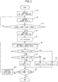
- FIG. 2 is a flowchart detailing the operation of the power supply device for an electric discharge machine of FIG. 1 . This flow is executed every time the pulse signal P is switched from off to on, mainly by each element of the control unit 10, based on the control computer program stored in the storage unit of the control unit 10.
- the ON-OFF control unit 10b outputs pulse signals S1, S2, S3, S4 for turning on all of the NMOS transistors 7a, 7b, 7c, 7d to the NMOS transistors 7a, 7b, 7c, 7d, respectively (step S1).
- the current value control unit 10b acquires the current value I d (step S2).
- the ON-OFF control unit 10b determines whether the current value I d has reached the target current I t (step S3). When the current value I d has not reached the target current It, the process returns to step S3 (No in step S3). Conversely, when the current value I d has reached the target current It (Yes in step S3), the ON-OFF control unit 10b outputs the pulse signals S1, S2, S3, S4 for turning off all of the NMOS transistors 7a, 7b, 7c, 7d to the NMOS transistors 7a, 7b, 7c, 7d, respectively (step S4).
- the ON-OFF control unit 10b starts the switching cycle of any of the NMOS transistors 7a, 7b, 7c, 7d (step S5).
- the ON-OFF control unit 10b starts the counting of a cycle counter (not illustrated) corresponding to the NMOS transistor for which the switching cycle has started (for example, the NMOS transistor 7a) (step S6). Furthermore, in step S6, the current value acquisition unit 10a acquires the current value I d .
- the ON-OFF control unit 10b determines whether the current value I d is greater than the target upper limit (step S7).
- the ON-OFF control unit 10b sets the ON-period of the NMOS transistor for which the switching cycle has started to T c and outputs a corresponding pulse signal to the NMOS transistor (step S8).
- the ON-OFF control unit 10b determines whether the current value I d is less than the target lower limit (step S9). When the current value I d is less than the target lower limit (Yes in step S9), the ON-OFF control unit 10b sets the ON-period of the NMOS transistor for which the switching cycle has started to T b and outputs a corresponding pulse signal to the NMOS transistor (step S10).
- the ON-OFF control unit 10b sets the ON-period of the NMOS transistor for which the switching cycle has started to T a and outputs a corresponding pulse signal to the NMOS transistor (step S11).
- step S12 the ON-OFF control unit 10b determines whether the pulse signal P has fallen (step S12). When the pulse signal P has fallen (Yes in step S12), the control unit 10 ends the process. Conversely, when the pulse signal P has not fallen (No in step S12), the ON-OFF control unit 10b increases the count of the cycle counter corresponding to the NMOS transistor for which the switching cycle has started by 1/4 cycle (step S13), and the process returns to step S6.
- the ON-period T b of the NMOS transistors 7a, 7b, 7c, 7d refers to the ON-period until the current value I d becomes less than the target lower limit and then reaches the target current I t
- the ON-period T c refers to the ON-period until the current value I d reaches the target current I t after the current value I d has become greater than the target upper limit.
- FIG. 3 is a timing chart detailing the operation of the power supply device for an electric discharge machine of FIG. 1
- FIG. 4 is an enlarged view of portion A of the timing chart of FIG. 3
- FIG. 5 is an enlarged view of portion B of the timing chart of FIG. 3 .
- (a) represents the pulse signal P
- (b) represents the voltage of the electrode gap 4
- (c) represents the current value I d .
- (d), (e), and (f) represent the current flowing through the NMOS transistor 7a, the switching cycle of the NMOS transistor 7a, and the pulse signal S1, respectively.
- (g), (h), and (i) represent the current flowing through the NMOS transistor 7b, the switching cycle of the NMOS transistor 7b, and the pulse signal S2, respectively.
- (j), (k), and (1) represent the current flowing through the NMOS transistor 7c, the switching cycle of the NMOS transistor 7c, and the pulse signal S3, respectively.
- (m), (n), and (o) represent the current flowing through the NMOS transistor 7d, the switching cycle of the NMOS transistor 7d, and the pulse signal S4, respectively.
- the current value acquisition unit 10a acquires the current value I d each time a rise of any of the switching cycles of the NMOS transistors 7a, 7b, 7c, 7d is detected.
- the ON-period of the NMOS transistor 7d is T s .
- the ON-period of the NMOS transistor 7b is T b .
- the operation of setting the ON-period of the NMOS transistor 7b to T b at time t5 corresponds to the process of Yes in step S7 and the process of step S8.
- the ON-period of the NMOS transistor 7c is T c .
- the operation of setting the ON-period of the NMOS transistor 7c to T c at time t6 corresponds to the process of Yes in step S9 and the process of step S10.
- the ON-period of the NMOS transistor 7a is T a .
- the switching frequency when the NMOS transistors 7a, 7b, 7c, 7d are switched from off to on in a predetermined order for each 90° phase timing is a switching frequency which is four times the switching frequency of a single NMOS transistor. Since current ripples decrease in inverse proportion to the switching frequency, the magnitude of the current ripples generated in the electrode gap 4 is a magnitude corresponding to 1/4 of the magnitude of the current ripples generated in the electrode gap 4 when a single NMOS transistor is turned on and off. Therefore, current ripples can be reduced.
- the heat generated by the switching loss of the NMOS transistors 7a, 7b, 7c, 7d is distributed among the NMOS transistors 7a, 7b, 7c, 7d, the effect of heat generation is eliminated, and the capability of each of the plurality of switching elements can be improved.
- the ON-period of the NMOS transistors 7a, 7b, 7c, 7d is increased when the current value I d becomes less than the target lower limit and the ON-period of the NMOS transistors 7a, 7b, 7c, 7d is reduced when the current value I d becomes greater than the target upper limit, the current value I d can be prevented from deviating significantly from the target current.
- the energy stored in the power supply device 1 for an electric discharge machine immediately after the NMOS transistors 7a, 7b, 7c, 7d are switched from on to off can be reduced
- the number of NMOS transistors may be two, three, five, or more, and when the number of NMOS transistors is two, the two NMOS transistors 7 are switched from off to on in a predetermined order at each phase timing of 180°.
- at least one of the diodes 8a, 8b, 8d, 8d, 9a, 9b, 9c, 9d may be omitted.
- PMOS transistors or the like may be used as the switching elements.
Landscapes
- Engineering & Computer Science (AREA)
- Mechanical Engineering (AREA)
- Manufacturing & Machinery (AREA)
- Electrical Discharge Machining, Electrochemical Machining, And Combined Machining (AREA)
Abstract
Description
- The present invention relates to a power supply device for an electric discharge machine.
- In electric discharge machines in which a workpiece is subjected to electric discharge machining (for example, die-sinking electric discharge machining), a power supply device in which a pulsed current is supplied to an electrode gap composed of a workpiece and an electrode which are opposed to each other with a predetermined gap is used. Such a power supply device for an electric discharge machine comprises a DC power supply which is connected in parallel to the electrode gap to apply a voltage for generating a current to the electrode gap, and a switching element which is arranged between the electrode gap and the DC power supply, and the electrode gap and the switching element are connected via a cable.
- Conventionally, power supply devices for an electric discharge machine which reduce current ripples, which cause electrode degradation, have been proposed (for example, Patent Literature 1). Current ripples can be reduced by increasing the switching frequency of the switching element or by arranging a smoothing inductor (for example, a coil) having a high inductance value in the cable.
- [PTL 1]
Japanese Unexamined Patent Publication (Kokai) No. 07-9255 - However, when the switching frequency of a switching element is increased to reduce current ripples, since switching loss of the switching element increases as the switching frequency increases, the heat of the switching element increases, and therefore, there is a problem in that the adverse effect of heat generation is exhibited.
- When a smoothing inductor having a high inductance value is arranged in the cable to reduce current ripples, the workpiece machining speed may be reduced due to the lengthening of the time from the start of current until peak current is reached.
- Furthermore, when a smoothing inductor having a high inductance value is arranged in the cable in order to reduce current ripple, since the energy stored in the power supply device for an electric discharge machine increases immediately after switching the switching element from on to off, the time from the start of current fall until the current value reaches zero becomes long, whereby an abnormal arc discharge may occur.
- An object of the present invention is to provide a power supply device for an electric discharge machine which can reduce current ripples without adverse effects due to the amount of heat generated, a decrease in workpiece machining speed, and abnormal arc discharge.
- The power supply device for an electric discharge machine according to the preset invention is for supplying a pulsed current to an electrode gap constituted by a workpiece and an electrode, which are opposed to each other with a predetermined gap, for electric discharge machining a workpiece, and the power supply device comprises a DC power supply which is connected in parallel to the electrode gap for applying a voltage for generating the current to the electrode gap, a plurality of switching elements which are in parallel to each other and which are arranged between the electrode gap and the DC power supply, a current value acquisition unit for acquiring a value of the current, and an ON-OFF control unit which, during the time when the current value reaches a predetermined value until the time when the current starts to fall, sets a cycle for switching the plurality of switching elements from off to on to the same cycle, switches the plurality of switching elements from off to on in a predetermined order for each timing of a predetermined phase, sets an ON-period of each of the plurality of switching elements based on a difference between the value of the current and the predetermined value, and performs ON-OFF control of the plurality of switching elements based on the cycle, the timing, and the ON-period.
- According to the present invention, the cycle for switching the plurality of switching elements from off to on during the period from the time when the current value reaches the predetermined value until the current starts to fall are set to be identical. Furthermore, the plurality of switching elements are switched from off to on in a predetermined order for each timing of a predetermined phase during the period from the time when the current value reaches the predetermined value until the current starts to fall. The ON-period of each of the plurality of switching elements is set based on the difference between the current value and the predetermined value during the period from the time when the current value reaches the predetermined value until the current starts to fall. Further, ON-OFF control of the plurality of switching elements is performed based on the cycle, timing, and ON-period during the period from the time when the current value reaches the predetermined value until the current starts to fall. The switching frequency when the plurality of switching elements are switched from off to on in a predetermined order for each predetermined timing of a phase in this manner is a switching frequency corresponding to the value obtained by multiplying the switching frequency of a single switching element by the number of the plurality of switching elements. Since current ripples decrease in inverse proportion to the switching frequency, the magnitude of the current ripples generated in the electrode gap by the power supply device for an electric discharge machine according to the present invention is approximately equivalent to the value obtained by dividing the magnitude of the ripples of the current that occurs in the electrode gap when a single switching element is turned on and off by the number of the plurality of switching elements. Therefore, current ripples can be reduced.
- Furthermore, according to the present invention, since the heat generated by the switching loss of the switching elements is distributed among the plurality of switching elements, the influence of heat can be eliminated and the capacity of each of the plurality of switching elements can be improved.
- Further, according to the present invention, since there is no need to provide a smoothing inductor having a high inductance value to reduce current ripple, there is neither a decrease in workpiece machining speed nor an abnormal arc discharge, which occurs when a smoothing inductor having a high inductance value is provided.
- Preferably, the predetermined timing of a phase is a uniform timing equal to the value obtained by dividing 360° by the number of the plurality of switching elements. As a result, variations in the magnitude of the current ripples can be reduced.
- Preferably, the ON-OFF control unit reduces the ON-period when the value of the current becomes greater than a first threshold value, which is greater than the predetermined value, and increases the ON-period when the value of the current is less than a second threshold value, which is less than the predetermined value. As a result, the current value can be prevented from deviating significantly from the predetermined value corresponding to peak current, which is the target current.
- Preferably, a current regeneration unit for regenerating the current is arranged between a first connection point between the electrode gap and one of the plurality of switching elements and a second connection point between the electrode gap and the DC power supply. As a result, the energy stored in the power supply device for an electric discharge machine can be reduced immediately after a switching element is switched from on to off.
-
-
FIG. 1 is a view showing a circuit of a power supply device for an electric discharge machine according to an embodiment of the present invention. -
FIG. 2 is a flowchart detailing the operation of the power supply device for an electric discharge machine ofFIG. 1 . -
FIG. 3 is a timing chart detailing the operation of the power supply device for an electric discharge machine ofFIG. 1 -
FIG. 4 is an enlarged view of portion A of the timing chart ofFIG. 3 . -
FIG. 5 is an enlarged view of portion B of the timing chart ofFIG. 3 . - The embodiments of the power supply device for an electric discharge machine according to the present invention will be described in detail below while referring to the drawings.
-
FIG. 1 is a view showing a circuit of the power supply device for an electric discharge machine according to an embodiment of the present invention. InFIG. 1 , thepower supply device 1 for an electric discharge machine supplies pulsed current for electric discharge machining aworkpiece 2, which is immersed in an electric discharge machining liquid in a machining tank (neither illustrated), to anelectrode gap 4 constituted by theworkpiece 2 and anelectrode 3, which are opposed to each other with a predetermined gap, via acable 5. - The
power supply device 1 for an electric discharge machine comprises aDC power supply 6,NMOS transistors diodes control unit 10. - The
DC power supply 6 is connected in parallel to theelectrode gap 4 for applying a voltage for generating current to theelectrode gap 4. The pulsed voltage applied to theelectrode gap 4 is, for example, 75 to 160 V, and has a frequency from approximately 1 KHz to several tens of KHz. In the present embodiment, the positive side of theDC power supply 6 is connected to theelectrode 3 and the negative side of theDC power supply 6 is connected to theworkpiece 2 via ashunt resistor 11. - The
NMOS transistor 7a is arranged between thecable 5 and the positive side of theDC power supply 6. TheNMOS transistor 7b is connected in parallel to theNMOS transistor 7a, and is arranged between theelectrode 3 and the positive side of theDC power supply 6. In the present embodiment, one end of theNMOS transistor 7b is connected to aconnection point 21 between the positive side of theDC power supply 6 and theNMOS transistor 7a via aconnection point 22 between theconnection point 21 and one end of theNMOS transistor 7b, and the other end of theNMOS transistor 7b is connected to aconnection point 23 between thecable 5 and the positive side of theDC power supply 6. - The
NMOS transistor 7c is connected in parallel to theNMOS transistors electrode 3 and the positive side of theDC power supply 6. In the present embodiment, one end of theNMOS transistor 7c is connected to aconnection point 24 between theconnection point 22 and one end of theNMOS transistor 7c, and the other end of theNMOS transistor 7c is connected to aconnection point 25 between thecable 5 and theconnection point 23. - The
NMOS transistor 7d is connected in parallel to theNMOS transistors electrode 3 and the positive side of theDC power supply 6. In the present embodiment, one end of theNMOS transistor 7d is connected to theconnection point 24, and the other end of theNMOS transistor 7d is connected to aconnection point 26 between thecable 5 and theconnection point 25. - Therefore, the
NMOS transistors electrode 3 and the positive side of theDC power supply 6. TheNMOS transistors - The
diode 8a is provided for backflow prevention, and has an anode which is connected to theconnection point 23 and a cathode which is connected to theNMOS transistor 7a. Thediode 8b is provided for backflow prevention, and has an anode which is connected to theconnection point 23 and a cathode which is connected to theNMOS transistor 7b. Thediode 8c is provided for backflow prevention, and has an anode which is connected to theconnection point 25 and a cathode which is connected to theNMOS transistor 7c. Thediode 8d is provided for backflow prevention, and has an anode which is connected to aconnection point 26 and a cathode which is connected to theNMOS transistor 7d. - The
diode 9a is provided for regenerating current immediately after theNMOS transistor 7a is switched from on to off, and is arranged between aconnection point 27 between theNMOS transistor 7a and the cathode of thediode 8a and aconnection point 28 between theelectrode gap 4 and the negative side of theDC power supply 6. Theconnection point 27 is an example of a first connection point and theconnection point 28 is an example of a second connection point. - The
diode 9b is provided for regenerating current immediately after theNMOS transistor 7b is switched from on to off, and is arranged between aconnection point 29 between theNMOS transistor 7b and the cathode of thediode 8b and aconnection point 30 between theelectrode gap 4 and theconnection point 28. Theconnection point 29 is an example of a first connection point and theconnection point 30 is an example of a second connection point. - The diode 9c is provided for regenerating current immediately after the
NMOS transistor 7c is switched from on to off, and is arranged between aconnection point 31 between theNMOS transistor 7c and the cathode of thediode 8c and aconnection point 32 between theelectrode gap 4 and theconnection point 30. Theconnection point 31 is an example of a first connection point and theconnection point 32 is an example of a second connection point. - The
diode 9d is provided for regenerating current immediately after theNMOS transistor 7d is switched from on to off, and is arranged between aconnection point 33 between theNMOS transistor 7d and the cathode of thediode 8d and aconnection point 34 between theelectrode gap 4 and theconnection point 32. Theconnection point 33 is an example of a first connection point and theconnection point 34 is an example of a second connection point. - The
diodes - The
control unit 10 is constituted by, for example, a field-programmable gate array (FPGA), and comprises a currentvalue acquisition unit 10a and an ON-OFF control unit 10b. - The current
value acquisition unit 10a is connected to aconnection point 35 between theconnection point 34 and one end of theshunt resistor 11 and aconnection point 36 between the other end of theshunt resistor 11 and theworkpiece 2, and has a current-sense amplifier (not illustrated) which amplifies and outputs voltage at both ends of theshunt resistor 11 corresponding to the value of the current flowing through theelectrode gap 4. - Furthermore, the current
value acquisition unit 10a acquires the value of the current flowing through theelectrode gap 4 by converting the value of the voltage output from the current-sense amplifier to a current value based on a table, which represents the relationship between voltage and current, stored in a storage unit (not illustrated) of thecontrol unit 10. Further, the currentvalue acquisition unit 10a provides data of the acquired current value Id to the ON-OFF control unit 10b. - In addition to the table which represents the relationship between voltage and current, data on a target current It, a target upper limit, and a target lower limit, which will be described later, as well as a control computer program are stored in the storage unit of the
control unit 10. - The ON-
OFF control unit 10b receives as input a pulse signal P which is generated by apulse generation circuit 13 based on pulse generation conditions corresponding to the machining conditions settings of theworkpiece 2 set in anNC device 12 automatically or by an operator. The machining conditions settings for theworkpiece 2 are determined in accordance with the material of theworkpiece 2, the material of theelectrode 3, the machining shape of theworkpiece 2, etc. The pulse generation conditions include a pulse wave on/off time, the number of pulses of the pulse wave, a pulse pause time, etc. - Further, the ON-
OFF control unit 10b generates a pulse signal S1 for turning on or off theNMOS transistor 7a, a pulse signal S2 for turning on or off theNMOS transistor 7b, a pulse signal S3 for turning on or off theNMOS transistor 7c, and a pulse signal S4 for turning on or off theNMOS transistor 7d based on the data of the current value Id and the pulse signal P. - In the present embodiment, the ON-
OFF control unit 10b sets the switching cycles at which theNMOS transistors - Furthermore, the ON-
OFF control unit 10b switches theNMOS transistor 7a, theNMOS transistor 7b, and theNMOS transistors OFF control unit 10b switches theNMOS transistors - The timing of a phase of 90° is an example of a timing of a phase of a value obtained by dividing 360° by the number of the plurality of switching elements. The phase timings need not be uniform in this manner, may be predetermined, may be 360° in one cycle, and may be, for example, 80°,100°, 80° and 100°. Furthermore, the ON-
OFF control unit 10b determines the switching cycle of each of theNMOS transistors NMOS transistors control unit 10. The timing at which the switching cycle of each of theNMOS transistors NMOS transistors - Furthermore, the ON-
OFF control unit 10b sets the ON-period of each of theNMOS transistors - In the present embodiment, the ON-
OFF control unit 10b reduces the ON-period of the NMOS transistor that is switched from off to on among theNMOS transistors - Furthermore, in the present embodiment, the ON-
OFF control unit 10b increases the ON-period ofNMOS transistor NMOS transistors - For example, if the ON-period of the
NMOS transistors NMOS transistors NMOS transistors 

- For example, the ON-period Ta is 1/8 of the switching cycle, the ON-period Tb is 1/4 of the switching cycle, and the ON-period Tc is 1/16 of the switching cycle.
- Further, the ON-
OFF control unit 10b performs ON-OFF control of theNMOS transistors NMOS transistor -
FIG. 2 is a flowchart detailing the operation of the power supply device for an electric discharge machine ofFIG. 1 . This flow is executed every time the pulse signal P is switched from off to on, mainly by each element of thecontrol unit 10, based on the control computer program stored in the storage unit of thecontrol unit 10. - First, the ON-
OFF control unit 10b outputs pulse signals S1, S2, S3, S4 for turning on all of theNMOS transistors NMOS transistors - Next, the current
value control unit 10b acquires the current value Id (step S2). Next, the ON-OFF control unit 10b determines whether the current value Id has reached the target current It (step S3). When the current value Id has not reached the target current It, the process returns to step S3 (No in step S3). Conversely, when the current value Id has reached the target current It (Yes in step S3), the ON-OFF control unit 10b outputs the pulse signals S1, S2, S3, S4 for turning off all of theNMOS transistors NMOS transistors - Next, the ON-
OFF control unit 10b starts the switching cycle of any of theNMOS transistors - The ON-
OFF control unit 10b starts the counting of a cycle counter (not illustrated) corresponding to the NMOS transistor for which the switching cycle has started (for example, theNMOS transistor 7a) (step S6). Furthermore, in step S6, the currentvalue acquisition unit 10a acquires the current value Id. - Next, the ON-
OFF control unit 10b determines whether the current value Id is greater than the target upper limit (step S7). When the current value Id is greater than the target upper limit (Yes in step S7), the ON-OFF control unit 10b sets the ON-period of the NMOS transistor for which the switching cycle has started to Tc and outputs a corresponding pulse signal to the NMOS transistor (step S8). - Conversely, when the current value Id is not greater than the target upper limit (No in step S7), the ON-
OFF control unit 10b determines whether the current value Id is less than the target lower limit (step S9). When the current value Id is less than the target lower limit (Yes in step S9), the ON-OFF control unit 10b sets the ON-period of the NMOS transistor for which the switching cycle has started to Tb and outputs a corresponding pulse signal to the NMOS transistor (step S10). - Conversely, when the current value Id is not less than the target lower limit (No in step S9), the ON-
OFF control unit 10b sets the ON-period of the NMOS transistor for which the switching cycle has started to Ta and outputs a corresponding pulse signal to the NMOS transistor (step S11). - After step S8, step S10, or step S11, the ON-
OFF control unit 10b determines whether the pulse signal P has fallen (step S12). When the pulse signal P has fallen (Yes in step S12), thecontrol unit 10 ends the process. Conversely, when the pulse signal P has not fallen (No in step S12), the ON-OFF control unit 10b increases the count of the cycle counter corresponding to the NMOS transistor for which the switching cycle has started by 1/4 cycle (step S13), and the process returns to step S6. - As used herein, the ON-period Tb of the
NMOS transistors -
FIG. 3 is a timing chart detailing the operation of the power supply device for an electric discharge machine ofFIG. 1 ,FIG. 4 is an enlarged view of portion A of the timing chart ofFIG. 3 , andFIG. 5 is an enlarged view of portion B of the timing chart ofFIG. 3 . - In the timing chart of
FIG. 3 , one cycle of a plurality of rising and falling cycles of the pulse signal P supplied to the ON-OFF control unit 10b for machining theworkpiece 2 will be described. - Furthermore, in the timing chart of
FIG. 3 , the cases in which the current value Id becomes less than the target lower limit during the period represented by portion A and the current value Id becomes greater than the target upper limit during the period represented by portion B will be described. - In
FIG. 3 , (a) represents the pulse signal P, (b) represents the voltage of theelectrode gap 4, and (c) represents the current value Id. Furthermore, inFIG. 3 , (d), (e), and (f) represent the current flowing through theNMOS transistor 7a, the switching cycle of theNMOS transistor 7a, and the pulse signal S1, respectively. Furthermore, inFIG. 3 , (g), (h), and (i) represent the current flowing through theNMOS transistor 7b, the switching cycle of theNMOS transistor 7b, and the pulse signal S2, respectively. Furthermore, inFIG. 3 , (j), (k), and (1) represent the current flowing through theNMOS transistor 7c, the switching cycle of theNMOS transistor 7c, and the pulse signal S3, respectively. Furthermore, inFIG. 3 , (m), (n), and (o) represent the current flowing through theNMOS transistor 7d, the switching cycle of theNMOS transistor 7d, and the pulse signal S4, respectively. - In the timing chart of
FIG. 3 , the currentvalue acquisition unit 10a acquires the current value Id each time a rise of any of the switching cycles of theNMOS transistors - When the pulse signal P rises at time t1, all of the
NMOS transistors electrode gap 4 by theDC power supply 6. The operation for switching all of theNMOS transistors FIG. 2 . - When dielectric breakdown occurs in the
electrode gap 4 at time t2 and the current value Id reaches the target current at time t3 due to the dielectric breakdown, all of theNMOS transistors NMOS transistors FIG 2 . Furthermore, the operation in which the currentvalue acquisition unit 10a acquires the current value Id each time a rise of any of the switching cycles of theNMOS transistors FIG 2 . - When the current value Id is greater than the target lower limit at time t4 when the waveform of the switching cycle of the
NMOS transistor 7d rises, the ON-period of theNMOS transistor 7d is Ts. When the current value Id is less than the target lower limit at time t5 when the waveform of the switching cycle of theNMOS transistor 7a rises, the ON-period of theNMOS transistor 7b is Tb. The operation of setting the ON-period of theNMOS transistor 7b to Tb at time t5 corresponds to the process of Yes in step S7 and the process of step S8. - When the current value Id is greater than the target upper limit at time t6 when the waveform of the switching cycle of the
NMOS transistor 7d rises, the ON-period of theNMOS transistor 7c is Tc. The operation of setting the ON-period of theNMOS transistor 7c to Tc at time t6 corresponds to the process of Yes in step S9 and the process of step S10. When the current value Id becomes less than the target upper limit and falls between the target upper limit and the target current It at time t7 when the waveform of the switching cycle of theNMOS transistor 7a rises, the ON-period of theNMOS transistor 7a is Ta. - When the pulse signal P falls at time t8, the current value Id falls and becomes zero at time t9. This process corresponds to the process of Yes in step S12. Furthermore, each time the waveform of the switching cycle of any of the
NMOS transistors NMOS transistors - The switching frequency when the
NMOS transistors electrode gap 4 is a magnitude corresponding to 1/4 of the magnitude of the current ripples generated in theelectrode gap 4 when a single NMOS transistor is turned on and off. Therefore, current ripples can be reduced. - Furthermore, according to the present embodiment, since the heat generated by the switching loss of the
NMOS transistors NMOS transistors - Furthermore, according to the present embodiment, since there is no need to provide a smoothing inductor having a high inductance value to reduce current ripple, there is neither a decrease in the
workpiece 2 machining speed nor abnormal arc discharge, which occurs when a smoothing inductor having a high inductance value is provided. - Furthermore, according to the present embodiment, since the ON-period of the
NMOS transistors NMOS transistors - Further, according to the present embodiment, by arranging
diodes power supply device 1 for an electric discharge machine immediately after theNMOS transistors - The present invention is not limited to the embodiments described above, and various changes and modifications can be made. For example, the number of NMOS transistors may be two, three, five, or more, and when the number of NMOS transistors is two, the two
NMOS transistors 7 are switched from off to on in a predetermined order at each phase timing of 180°. Furthermore, at least one of thediodes -
- 1 power supply device for electric discharge machine
- 2 workpiece
- 3 electrode
- 4 electrode gap
- 5 cable
- 6 DC power supply
- 7a, 7b, 7c, 7d NMOS transistor
- 8a, 8b, 8c, 8d, 9a, 9b, 9c, 9d diode
- 10 control unit
- 10a current value acquisition unit
- 10b ON-OFF control unit
- 11 shunt resistor
- 12 NC device
- 13 pulse generation circuit
- 21, 22, 23, 24, 25, 26, 27, 28, 29, 30, 31, 32, 33, 34, 35, 36 connection point
Claims (4)
- A power supply device for an electric discharge machine for supplying a pulsed current to an electrode gap constituted by a workpiece and an electrode, which are opposed to each other with a predetermined gap, for electric discharge machining a workpiece, the power supply device comprising:a DC power supply which is connected in parallel to the electrode gap for applying a voltage for generating the current to the electrode gap,a plurality of switching elements which are in parallel to each other and which are arranged between the electrode gap and the DC power supply,a current value acquisition unit for acquiring a value of the current, andan ON-OFF control unit which, during the time when the current value reaches a predetermined value until the time when the current starts to fall, sets a cycle for switching the plurality of switching elements from off to on to the same cycle, switches the plurality of switching elements from off to on in a predetermined order for each timing of a predetermined phase, sets an ON-period of each of the plurality of switching elements based on a difference between the value of the current and the predetermined value, and performs ON-OFF control of the plurality of switching elements based on the cycle, the timing, and the ON-period.
- The power supply device for an electric discharge machine according to claim 1, wherein the timing of a predetermined phase is an equal phase timing of a value obtained by dividing 360° by the number of the plurality of switching elements.
- The power supply device for an electric discharge machine according to claim 1 or 2, wherein the ON-OFF control unit reduces the ON-period when the value of the current becomes greater than a first threshold value, which is greater than the predetermined value, and increases the ON-period when the value of the current is less than a second threshold value, which is less than the predetermined value.
- The power supply device for an electric discharge machine according to any one of claims 1 to 3, wherein a current regeneration unit for regenerating the current is arranged between a first connection point between the electrode gap and one of the plurality of switching elements and a second connection point between the electrode gap and the DC power supply.
Applications Claiming Priority (1)
| Application Number | Priority Date | Filing Date | Title |
|---|---|---|---|
| PCT/JP2018/040624 WO2020090073A1 (en) | 2018-10-31 | 2018-10-31 | Power source device for electric discharge machine |
Publications (2)
| Publication Number | Publication Date |
|---|---|
| EP3875202A1 true EP3875202A1 (en) | 2021-09-08 |
| EP3875202A4 EP3875202A4 (en) | 2022-07-06 |
Family
ID=70462962
Family Applications (1)
| Application Number | Title | Priority Date | Filing Date |
|---|---|---|---|
| EP18938322.7A Pending EP3875202A4 (en) | 2018-10-31 | 2018-10-31 | POWER SOURCE DEVICE FOR ELECTRIC SHOCK MACHINE |
Country Status (5)
| Country | Link |
|---|---|
| US (1) | US11794263B2 (en) |
| EP (1) | EP3875202A4 (en) |
| JP (1) | JP7032561B2 (en) |
| CN (1) | CN112930238B (en) |
| WO (1) | WO2020090073A1 (en) |
Family Cites Families (15)
| Publication number | Priority date | Publication date | Assignee | Title |
|---|---|---|---|---|
| JPS61182721A (en) * | 1985-02-07 | 1986-08-15 | Amada Co Ltd | Electric discharge circuit of electric discharge machine |
| DE4017207A1 (en) * | 1989-07-24 | 1991-12-05 | Boehringer Andreas | Electrical supply with high current change speeds - using several current adjusters with symmetrically offset pulsed current cycles producing reduced inductivity in smoothing valve |
| JPH0484672A (en) * | 1990-07-26 | 1992-03-17 | I N R Kenkyusho:Kk | Pulse power unit for energizing |
| US5539178A (en) * | 1992-11-18 | 1996-07-23 | Mitsubishi Denki Kabushiki Kaisha | Method and apparatus for controlling the power supply for electrical discharge machine |
| JP2914103B2 (en) | 1993-06-30 | 1999-06-28 | 三菱電機株式会社 | Electric discharge machine |
| JPH08118148A (en) * | 1994-10-19 | 1996-05-14 | Fanuc Ltd | Power supply unit for electric discharge machine |
| JP3245087B2 (en) * | 1997-05-12 | 2002-01-07 | 三菱電機株式会社 | Power supply unit for electric discharge machine |
| CN1325215C (en) * | 2004-08-27 | 2007-07-11 | 哈尔滨工业大学 | Cyclic superimposed chopper energy-saving pulse power source for spark machining |
| ES2353520T3 (en) * | 2005-08-01 | 2011-03-02 | Agie Charmilles Sa | PROCEDURE OF OPERATION OF A MACHINING MACHINE BY ELECTROEROSION AND A SYSTEM OF MACHINING BY ELECTROEROSION. |
| JP2007301682A (en) * | 2006-05-11 | 2007-11-22 | Denso Corp | EDM machine |
| DE112008003599B4 (en) * | 2008-01-31 | 2015-04-23 | Mitsubishi Electric Corp. | discharge device |
| CN102143821B (en) * | 2008-09-02 | 2012-09-12 | 三菱电机株式会社 | Power supply device for electric discharge machine |
| JP4874358B2 (en) * | 2009-02-27 | 2012-02-15 | 株式会社ソディック | Power supply device for machining of Die-sinker EDM |
| US20120228268A1 (en) * | 2011-02-25 | 2012-09-13 | Mitsubishi Electric Corporation | Power supply device for electrical discharge machine and control method therefor |
| CN103958103B (en) * | 2011-11-30 | 2016-12-28 | 三菱电机株式会社 | Electric discharge machine supply unit |
-
2018
- 2018-10-31 EP EP18938322.7A patent/EP3875202A4/en active Pending
- 2018-10-31 US US17/290,481 patent/US11794263B2/en active Active
- 2018-10-31 JP JP2020554699A patent/JP7032561B2/en active Active
- 2018-10-31 WO PCT/JP2018/040624 patent/WO2020090073A1/en not_active Ceased
- 2018-10-31 CN CN201880098684.XA patent/CN112930238B/en active Active
Also Published As
| Publication number | Publication date |
|---|---|
| CN112930238B (en) | 2024-03-29 |
| US11794263B2 (en) | 2023-10-24 |
| EP3875202A4 (en) | 2022-07-06 |
| US20210370425A1 (en) | 2021-12-02 |
| CN112930238A (en) | 2021-06-08 |
| JP7032561B2 (en) | 2022-03-08 |
| WO2020090073A1 (en) | 2020-05-07 |
| JPWO2020090073A1 (en) | 2021-09-02 |
Similar Documents
| Publication | Publication Date | Title |
|---|---|---|
| KR101681120B1 (en) | Power supply device for wire electric discharge machining | |
| EP3396700A1 (en) | Power converter unit, plasma processing equipment and method of controlling several plasma processes | |
| EP2787628B1 (en) | Control method for inverter device, and inverter device | |
| EP1876699A2 (en) | Method for controlling brake chopper, brake chopper and frequency converter | |
| JP6810316B1 (en) | DC pulse power supply for plasma processing equipment | |
| JP2016140168A (en) | Device and method for voltage conversion | |
| CN100445007C (en) | Method and generator for electrical discharge machining | |
| WO2012114524A1 (en) | Power supply device for electric discharge machining machine and method for controlling same | |
| EP1498206B1 (en) | Machining power supply of wire electric discharge machine and power supply method | |
| KR101440747B1 (en) | Control circuit and interleave power supply provided with same | |
| US8963520B1 (en) | System and method to soft-start synchronous buck converters | |
| US11794263B2 (en) | Power source device for electric discharge machine | |
| JP4770953B2 (en) | Static eliminator | |
| CN106712270B (en) | Control method and control device of square wave uninterruptible power supply | |
| DE102018000827B4 (en) | motor drive device | |
| CN107959415B (en) | Delay control circuit for DC-DC converter | |
| US3472994A (en) | Electrical discharge machining apparatus for multiple electrodes | |
| US11752565B2 (en) | Power source device for electric discharge machine | |
| JPH11333632A (en) | Electric discharge machine | |
| JP2006094609A (en) | Power supply device | |
| JPS60172419A (en) | Power unit for electric discharge machining | |
| CN107666175B (en) | Control method and control device of square wave uninterrupted power supply | |
| EP3806307A1 (en) | Isolated dc/dc resonant converter and method for operating such a converter | |
| JPS6057972B2 (en) | Electric discharge machining equipment | |
| JP2000262046A (en) | Dc-to-dc converter |
Legal Events
| Date | Code | Title | Description |
|---|---|---|---|
| STAA | Information on the status of an ep patent application or granted ep patent |
Free format text: STATUS: THE INTERNATIONAL PUBLICATION HAS BEEN MADE |
|
| PUAI | Public reference made under article 153(3) epc to a published international application that has entered the european phase |
Free format text: ORIGINAL CODE: 0009012 |
|
| STAA | Information on the status of an ep patent application or granted ep patent |
Free format text: STATUS: REQUEST FOR EXAMINATION WAS MADE |
|
| 17P | Request for examination filed |
Effective date: 20210421 |
|
| AK | Designated contracting states |
Kind code of ref document: A1 Designated state(s): AL AT BE BG CH CY CZ DE DK EE ES FI FR GB GR HR HU IE IS IT LI LT LU LV MC MK MT NL NO PL PT RO RS SE SI SK SM TR |
|
| DAV | Request for validation of the european patent (deleted) | ||
| DAX | Request for extension of the european patent (deleted) | ||
| A4 | Supplementary search report drawn up and despatched |
Effective date: 20220607 |
|
| RIC1 | Information provided on ipc code assigned before grant |
Ipc: B23H 1/02 20060101AFI20220601BHEP |