EP3873588B1 - Artificial vision system - Google Patents
Artificial vision system Download PDFInfo
- Publication number
- EP3873588B1 EP3873588B1 EP19794568.6A EP19794568A EP3873588B1 EP 3873588 B1 EP3873588 B1 EP 3873588B1 EP 19794568 A EP19794568 A EP 19794568A EP 3873588 B1 EP3873588 B1 EP 3873588B1
- Authority
- EP
- European Patent Office
- Prior art keywords
- vision system
- artificial vision
- implant
- pixels
- visual prosthesis
- Prior art date
- Legal status (The legal status is an assumption and is not a legal conclusion. Google has not performed a legal analysis and makes no representation as to the accuracy of the status listed.)
- Active
Links
Images



Classifications
-
- A—HUMAN NECESSITIES
- A61—MEDICAL OR VETERINARY SCIENCE; HYGIENE
- A61N—ELECTROTHERAPY; MAGNETOTHERAPY; RADIATION THERAPY; ULTRASOUND THERAPY
- A61N1/00—Electrotherapy; Circuits therefor
- A61N1/18—Applying electric currents by contact electrodes
- A61N1/32—Applying electric currents by contact electrodes alternating or intermittent currents
- A61N1/36—Applying electric currents by contact electrodes alternating or intermittent currents for stimulation
- A61N1/36046—Applying electric currents by contact electrodes alternating or intermittent currents for stimulation of the eye
-
- A—HUMAN NECESSITIES
- A61—MEDICAL OR VETERINARY SCIENCE; HYGIENE
- A61N—ELECTROTHERAPY; MAGNETOTHERAPY; RADIATION THERAPY; ULTRASOUND THERAPY
- A61N1/00—Electrotherapy; Circuits therefor
- A61N1/02—Details
- A61N1/04—Electrodes
- A61N1/05—Electrodes for implantation or insertion into the body, e.g. heart electrode
- A61N1/0526—Head electrodes
- A61N1/0543—Retinal electrodes
-
- H—ELECTRICITY
- H02—GENERATION; CONVERSION OR DISTRIBUTION OF ELECTRIC POWER
- H02J—ELECTRIC POWER NETWORKS; CIRCUIT ARRANGEMENTS OR SYSTEMS FOR SUPPLYING OR DISTRIBUTING ELECTRIC POWER; SYSTEMS FOR STORING ELECTRIC ENERGY
- H02J50/00—Circuit arrangements or systems for wireless supply or distribution of electric power
- H02J50/30—Circuit arrangements or systems for wireless supply or distribution of electric power using light, e.g. lasers
-
- A—HUMAN NECESSITIES
- A61—MEDICAL OR VETERINARY SCIENCE; HYGIENE
- A61N—ELECTROTHERAPY; MAGNETOTHERAPY; RADIATION THERAPY; ULTRASOUND THERAPY
- A61N1/00—Electrotherapy; Circuits therefor
- A61N1/18—Applying electric currents by contact electrodes
- A61N1/32—Applying electric currents by contact electrodes alternating or intermittent currents
- A61N1/36—Applying electric currents by contact electrodes alternating or intermittent currents for stimulation
- A61N1/372—Arrangements in connection with the implantation of stimulators
- A61N1/378—Electrical supply
- A61N1/3787—Electrical supply from an external energy source
-
- H—ELECTRICITY
- H02—GENERATION; CONVERSION OR DISTRIBUTION OF ELECTRIC POWER
- H02J—ELECTRIC POWER NETWORKS; CIRCUIT ARRANGEMENTS OR SYSTEMS FOR SUPPLYING OR DISTRIBUTING ELECTRIC POWER; SYSTEMS FOR STORING ELECTRIC ENERGY
- H02J2105/00—Networks for supplying or distributing electric power characterised by their spatial reach or by the load
- H02J2105/40—Networks for supplying or distributing electric power characterised by their spatial reach or by the load characterised by the loads connecting to the networks or being supplied by the networks
- H02J2105/46—Medical devices, medical implants or life supporting devices
Definitions
- the present disclosure relates to visual prostheses, and particularly retinal implants.
- the present disclosure further relates to artificial vision systems comprising retinal implants. And also relates to methods for implanting the retinal implant and to methods for providing artificial vision.
- Retinitis pigmentosa is a genetic disorder of the eyes that causes loss of vision. Symptoms include trouble seeing at night and decreased peripheral vision (side vision).
- the underlying mechanism involves the progressive loss of photoreceptor cells in the back of the eye. In severe cases, a person goes blind because the photoreceptor cells are no longer sensitive to light. However, in most cases the neurons (Retina Ganglion Cell) of the retina are still functional.
- Such neurons can be stimulated with an electrical signal, and if such neurons are stimulated, the optical nerve transfers such stimulation to the visual cortex.
- US 2012/259410 discloses an apparatus for use with an external non-visible light source.
- the apparatus comprises an intraocular device configured for implantation in a human eye, and comprising an energy receiver.
- the energy receiver is configured to receive light emitted from the external non-visible light source, and extract energy from the emitted light for powering the intraocular device.
- the intraocular device is configured to regulate a parameter of operation of the intraocular device based on a modulation of the light emitted by the external non-visible light source and received by the energy receiver.
- US 2017/368351 discloses an intraocular apparatus for implantation in a subject's eye.
- the intraocular apparatus includes a photosensor array including a plurality of photosensors configured to receive an ambient image, and a power source, for powering the apparatus.
- the intraocular apparatus additionally including a flexible 0.4-3 mm electrical connector, connecting the photosensor array to the power source.
- US2004/181265 discloses a self-sufficient retinal prosthesis powered by intra-ocular photovoltaic cells illuminated only by ambient light is provided. Photovoltaic cells can be disposed at the periphery of the retina or in the anterior chamber of the eye. An adaptive retinal prosthesis is also provided, such that the number of pixels energized in the prosthesis is selected according to the variable available power from ambient light.
- a visual neuroprosthetic device includes an array of nanoscale waveguides, each nanoscale waveguide in the array having a photovoltaic material located between an internal conductor and an external conductor, wherein each nanoscale waveguide receives, propagates, and converts incident light into electrical neural signals.
- a miniature video camera housed in the patient's glasses captures a scene.
- the video is sent to a small patient-worn video processing unit where it is processed and transformed into instructions that are sent back to the glasses via a cable. These instructions are transmitted wirelessly to an antenna in the retinal implant.
- the signals are then sent to the electrode array, which emits small pulses of electricity. These pulses stimulate the retina's remaining cells, which transmit the visual information along the optic nerve to the brain, creating the perception of patterns of light. Patients learn to interpret these visual patterns with their retinal implant.
- the electrical signals are generated outside the sclera and sent via a cable to inside the eye.
- Each electrode generates an electric signal independently to excite the neurons underneath the retina's surface.
- the electrode array comprises 60 electrodes. Even though patients may recognize very basic shapes thanks to the 60 electrodes, it is clear that a patient may benefit from an increase in electrodes, and from an increased density of electrodes (i.e. electrodes per square area). More neurons or areas might be excited and thus more detailed information on shapes might be transmitted to the optical nerve, potentially leading to improved vision.
- an increase in the number of electrodes means an increase in power consumption and also in the size of data transfer to configure the matrix of electrodes for each frame image. It is evident that to increase the number of electrodes and still provide them with sufficient power is not a trivial matter.
- the present disclosure provides examples of systems and methods that at least partially resolve some of the aforementioned disadvantages.
- an artificial vision system comprises a visual prosthesis, and particularly a retinal implant, and further comprises a camera, an image processor for analysing a video signal from the camera to generate a data pattern, and a light source for emitting light according to the generated data pattern.
- the visual prosthesis comprises an integrated circuit comprising a plurality of pixels, and an array of electrodes attached to the pixels and configured to excite neurons in a retina.
- the prosthesis furthermore comprises one or more photovoltaic cells, and a photodetector, and the integrated circuit is configured to process signals form the photodetector to selectively activate the pixels.
- a functional kit is thus provided for operating the visual prosthesis.
- the retinal implant can be provided with many more individual electrodes or pixels which can increase the quality of vision for patients, as more detailed shapes may be excited.
- the photovoltaic (PV) cells can be powered by incoming lights. Incoming light flashes or pulses may be registered by the photodetector and the integrated circuit can analyse the received pulses and transform into a selective activation of the pixels. Incoming light can thus both be used to power the implant and to transmit information that might be obtained from a camera.
- signal quality can be maintained even if the number of pixels increases as the electrodes may be directly attached to the pixels of the integrated circuit. Crosstalk between wires can be effectively avoided.
- a visual prosthesis may be regarded as any visual device intended to (partly) restore functional vision in those suffering from partial or total blindness.
- the visual prosthesis may be a retinal implant.
- retinal implant is meant to cover epiretinal implants (i.e. implants which in use are positioned on the retina), subretinal implants (which are to be implanted behind the retina), and suprachoroidal implants (which are to be implanted between the choroid and the sclera).
- the visual prosthesis may comprise a capacitor, and optionally the capacitor is a graphene layer.
- the capacitor allows the storage of electrical energy derived from the PV cells.
- the integrated circuit may be an ASIC, i.e. a chip specifically developed for the specific use as herein described.
- the photodetector may be a PIN diode.
- the visual prosthesis may be configured to assume an unfolded state and a folded state.
- the provision of PV cells in the visual prosthesis means that the size of the implant is increased. This could lead to a more problematic process of implanting it. This can be at least partially resolved when the visual prosthesis can be implanted in a folded state, and once in an appropriate position within the eye, the implant can unfold.
- Shape memory material may be activated in a variety of ways, e.g. if the material is exposed to a change in temperature.
- the light source may comprise a LED.
- the LED may be configured to emit light with a wavelength in a range of 700 nm or more, particularly 750 nm or more, more particularly 800 nm or more. At these wavelengths, the light can be transmitted through the patient's eye (including lens, cornea and vitreous humor) without significant losses.
- a retinal implant may thus be used.
- the implant may be an epi-retinal implant, i.e. positioned within the retina.
- the PV cells if selected properly may function at high efficiency at these wavelengths.
- the implant may be a subretinal implant (i.e. behind the retina), or a suprachordial implant (between the choroid and sclera).
- the camera, the image processor and the light source are mounted on a support, and in particular on glasses.
- a patient may wear the glasses and the camera is therewith positioned close to the eyes and the images recorded by the camera are recorded from an angle of vision of the natural eyes.
- a method for implanting a retinal implant comprises: providing a retinal implant according to any of the examples herein disclosed, and making an incision in a sclera. After making the incision in the sclera, the retinal implant may be inserted through the incision, when the retinal implant is in a folded state. After insertion, the retinal implant may be unfolded.
- the retinal implant may be provided in a sheath, and unfolding the retinal implant comprises removing the sheath.
- a non-claimed method for providing artificial vision for a patient comprises recording an image, processing the recorded image to generate a pixelated image, and producing light pulses transmitting the generated pixelated image to a visual prosthesis.
- the visual prosthesis may be a retinal implant, and more specifically an epiretinal implant.
- data transmission using light is used for communication between a visual prosthesis and an image recording system (e.g. a camera or video camera).
- the light used for data transmission may be in the visual light spectrum, but preferably will be in the infrared range.
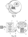
- FIG. 1 schematically illustrates a prior art retinal implant.
- the implant comprises an antenna A which receives signals from a further antenna which may be integrated in glasses worn by a user.
- the signals sent to antenna A may be the result of image processing of a video integrated in the glasses.
- Reference sign B refers to an electronic unit outside the eye. Individual electrical cables C lead from the electronics unit to electrode array D.
- FIGS 2A - 2D schematically illustrate a first example of a retina implant and an artificial vision system including such a retinal implant.
- the artificial vision system according to this example comprises an implant 100.
- the implant 100 may be an epiretinal implant.
- the system according to this example furthermore comprises a camera 10.
- the camera 10 may be a digital camera, and specifically a digital camera integrated in glasses that may be worn by a user.
- Recordings from camera 10 may be sent in real-time to an image processor 12 for analysing a video signal from the camera to generate a data pattern.
- the data pattern may be generated by infrared LED driver 18.
- the LED driver 18 in the example drives the flashing of LED 20.
- the flashing of LED may have a frequency of e.g. 1 MHz - 1 GHz, specifically 10 - 500 MHz. Both the LED driver 18 and LED 20 may be integrated in the same glasses worn by the user.
- the light flashes from LED 20 may be received by a photoreceptor 120 of implant 100.
- the photoreceptor 120 may be a PIN diode in some examples.
- Implant 100 includes an integrated circuit, i.e. a chip. Signals received by the photoreceptor 120 may be transformed into excitation signals for the electrodes 140.
- the photoreceptor and circuit may be programmed such that an incoming light flash causes an electric pulse and the electrical pulse is compared to a threshold. If the pulse is above the predetermined thresholds, a "1" is generated. If the pulse is below the threshold (e.g. absent), then a "0" is generated.
- a threshold e.g. absent
- the implant 100 may be powered by a photovoltaic cell array 110 connected to a suitable converter.
- FIG. 2B schematically illustrates a high level communication between the glasses 14 (or other support) including the camera, image processor and LED and implant 100.
- the glasses 14 in this example comprise a first radiofrequency transceiver (rf transmitter/receiver) and the implant 100 comprises a second rf transceiver.
- basic functionalities may be communicated through the rf transmitter, including synchronization of the glasses 14 (and thus the video signal and image processing) with the implant (and thus the excitation of individual electrodes), so that the excitation of electrodes is in accordance with the camera recordings.
- Other basic communications may include e.g. a fault communication, and an acknowledgement of receipt.
- FIG. 2C schematically illustrates that in this example, the PV array includes 9 PV cells 102A - 1021.
- the PV cells may be PERT cells which have a high efficiency.
- Each of the PV cells may have an area of 15 - 40 mm 2 , particularly approximately 25 mm 2 .
- 9 PV cells of each 5 by 5 mm may be used.
- the chip with the attached electrodes may also have a size of approximately 5 by 5 mm in this example.
- the number of pixels and electrodes may be e.g. 15 by 22, 20 by 30, or 25 by 33 or more. As compared to the prior art illustrated in figure 1 , the number of electrodes may thus be multiplied by 10 or more. Note that in these examples an approximate ratio of height to width of 2:3 is maintained. Variations with respect to this ratio are possible.
- PERT PV cells may be used with a thickness of approximately 100 microns, e.g. in the range of 50 - 300 microns.
- the number of PV cells, the type and the area occupied by the cells may be adjusted in accordance with energy needs. Also another shape may be selected for the PV array.
- the frequency of flashing of the LED is high enough, for example in the aforementioned frequency ranges, the light will be seen as substantially continuous by the PV cells, so that the performance is not negatively affected.
- photoreceptor 120 may be integrated.
- the LED 20 may be configured to emit light with a wavelength in a range of 700 nm or more, particularly 750 nm or more, more particularly 800 nm or more.
- the PV cells have a high efficiency, and moreover, the transmission through the human eye (including cornea, lens, vitreous humor) is high as well, for example 85% or more or 90% or more.
- the retinal implant 100 is configured to assume an unfolded state and a folded state.
- the implant 100 includes a first frame of shape memory material 114 which when activated forces the implant to the folded shape, and a second frame 116 of shape memory material which when activated forces the implant to the unfolded shape.
- the shape memory material may be thermally activated and particularly may include shape memory metal.
- the areas around the junctions between the columns of the PV cells may have a memory shape so that the junction is straight or folded.
- By sending an electrical current through the metal frame 114 or 116, one of the frames may be heated so that the frame has a tendency to assume its memory shape.
- the frame 114 If the frame 114 is activated, the junctions between the three columns will fold, such that the implant as a whole assumes the folded shape. If the frame 116 is activated, the junctions between the columns of cells will straighten out, such that the implant will assume an unfolded state.
- the temperature of transition from one shape to another shape may be well above 37oC, i.e. normal body temperature. If the temperature is chosen close to the average body temperature, a variation of temperature due to e.g. a fever may provoke a change of shape of the implant.
- the tendencies of the shape memory frames may be exchanged. It should also be clear that other shape memory materials and activation methods may be used.
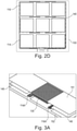
- Figure 2D shows the same PV cell array viewed from the opposite side.
- the bottom sides of the PV cells may be seen.
- a reflective layer may be provided, e.g. an aluminized mylar TM layer, to reflect back any possible incident photon that has passed through the PV cells.
- the chip with electrode array 140 may be arranged.
- FIGs 3A and 3B schematically illustrates an example of a retinal implant.
- three PV cells are shown, whereas in figure 2 nine PV cells were shown.
- the illustration in figure 3 may be understood as a separate example of the retinal implant, but it should be clear that the build-up shown in figure 3 may also be regarded as illustrating only a portion of the implant shown in figure 2 , i.e. the illustration in figure 3 should not be understood as limiting in size, number of PV cells etc.
- the retinal implant comprises a base 152 and the PV cells may be mounted on base 152.
- the base 152 may be e.g. a polyamide.
- the retinal implant further comprises a capacitor 145 to store energy generated by the PV cells.
- the capacitor 145 may be a graphene layer, and in particular an array of graphene areas 145 connected to each of the individual PV cells. If the same configuration is assumed as in figure 2 , there may be nine areas of approximately 5 mm by 5 mm of graphene.
- the thickness of the graphene layer may be e.g. between 50 and 500 microns. Assuming a thickness of approximately 100 microns, and assuming an estimated capacitance of at least 200 F/g, one may expect to store 18 Joules. If the capacitance of graphene is improved, or the area or thickness of graphene are increased, more energy may evidently be stored.
- an ASIC 135 may be provided on top of one of the PV cells.
- the ASIC may be provided on the central PV cell.
- An array of electrodes 140 may be attached to ASIC 135, in particular the electrodes may be mounted directly, i.e. deposited on the ASIC 135.
- a plurality of pixels may be defined which can be individually excited in accordance with the instructions received from the LED.
- the implant also comprises a top layer 151, and the top layer 151 may be made from polyamide.
- the top and bottom layers may serve the purpose of reducing the exposure of components of the implant to the surroundings.
- the top layer 151 may comprise a plurality of holes corresponding to the electrodes.
- Reference signs 114A and 116A illustrate stretches of shape memory material, which may in particular be located between PV cells, and particularly between rows of PV cells, such that the columns may be folded as illustrated in the example of figure 2 .
- the shape memory material may be metallic, and in the illustrated example, the shape memory material may be e.g. Nitinol.
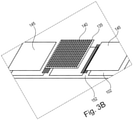
- Figure 3B illustrates the same implant (or part of implant) as shown in figure 3A .
- the top layer 150 has been removed in this figure.
- the ASIC 135 with electrodes 140 may easily be recognized, as well as graphene areas 145 placed on PV cells 102.
- the maximum thickness for the implant when folded is preferably below 1 mm.
- the thickness of the PV cells is chosen at 100 microns, and the same thickness is chosen for the graphene layer.
- FIGs 4A - 4G schematically illustrates a method of implanting according to an example.
- the implant illustrated in figure 4 substantially corresponds to the implant illustrated particularly in figure 2 , but the same method or similar methods may be used in different implants as well.
- an incision 70 may be made in a patient's eye.
- the implant 100 in this example is provided in a sheath 80.
- the implant as will become clear from the following figures, is in a folded state. A small incision is therefore sufficient for the introduction of the implant 100.
- Figures 4B and 4C schematically illustrate how implant 100 arranged within sheath 80 is inserted into the eye.
- FIG 4D it is shown how sheath 80 may be removed, while the implant is still in the folded state 100A.
- figure 4E an electrical current may be sent through the nitinol wires illustrated in the previous figures. By sending electrical current through the nitinol wires, these wires may heat up and thus assume their remembered shape.
- the remembered shape of a frame may be the unfolded or stretched out shape of the wires.
- implant starts to unfold, to assume in figure 4G the unfolded state 100B.
- the implant may be removed by sending electrical current through the other shape memory frame so increase the heat and stimulate that frame to assume its folded shape.
- the implant may be removed.
- ASIC 135 located below the PV cell is indicated for better reference.
- the implant may be designed to assume its unfolded state without any external stimulation. I.e. merely by removing the sheath 80, the implant will assume the unfolded shape.
- the implant including PV cells, photoreceptor, integrated circuit with pixels attached to electrodes is entirely placed within the eye.
- the previously illustrated wires for the prior art leading from outside the eye to inside the eye are thus avoided, while energy supply can be ensured.
- FIG. 5 schematically illustrates a further example of a retina implant 100 and an artificial vision system including such a retinal implant.
- the artificial vision system in this example includes a camera 10, an image processor 12 for analysing a video signal from the camera to generate a data pattern, and a light source 20 for emitting light according to the generated data pattern.
- the camera 10 and image processor may be arranged on an external unit or support 14, e.g. glasses worn by a patient.
- the functioning of the implant 100 and artificial vision system is largely comparable to the functioning of the example in figure 2 .
- the data pattern derived from the video signal after image processing is transmitted to the implant 100.
- the LED driver 18 in the example drives the flashing of LED 20. Data transmission in this example occurs through light.
- Photodetector diode 120 receives the light and the data pattern is analysed to stimulate the pixels as in the example of figure 2 .
- the light flashes from LED 20 may be received by a photoreceptor 120 of implant 100.
- the photoreceptor 120 may be a PIN diode in some examples.
- Implant 100 includes an integrated circuit, i.e. a chip. Signals received by the photoreceptor 120 may be transformed into excitation signals for the electrodes 140.
- the light is received by PV cells array 110 to provide power for the functioning of the implant 100.
- a further functionality is included. If and when a pixel is stimulated, the neurons situated behind and in the immediate vicinity are stimulated. There are however different types of neurons, and upon implanting the retinal implant, the precise disposition of pixels with respect to neurons is not known.
- neural activity may be derived (block 35) including information on the quantity and types of neurons underlying various pixels.
- the visualization of the image recorded by camera 10 may be improved for patients.
- information regarding neural activity may be correlated with specific pixels.
- the information regarding neural activity in relation with pixels may be transmitted to the image processor 12.
- the data may be transmitted through light as well.
- the retinal implant in this example includes a light source 30, e.g. a LED.
- the light signal emitted from LED 30 may be modulated to transmit data.
- the light may be received at photodetector 32.
- the signals received by photodetectors 32 may be analysed (block 45) and the information regarding neural activity in relation with individual pixels/electrodes may be stored and/or fed back (block 55) to the image processor 12.
- the knowledge on neural activity derived from previous stimulations may be used to improve the visual perception of the patient.
- the information feedback regarding neural activity (block 35) and transmission through LED 30 may be carried out at a lower frequency than the transmission of light from LED 20. In some examples, information may be gathered during some time before transmitting the information.
- the support 14 in this example comprise a first radiofrequency transceiver (rf transmitter/receiver) and the implant 100 comprises a second rf transceiver.
- Basic functionalities may be communicated through the rf transmitter, including synchronization of the glasses (and thus the video signal and image processing) with the implant (and thus the excitation of individual electrodes), so that the excitation of electrodes is in accordance with the camera recordings.
- Other basic communications may include e.g. a fault communication, and an acknowledgement of receipt.
- the synchronization also serves to correlate the electrode response that is measured with specific excitations of pixels.
- the second rf transmitter may also communicate the electrode impedance of the pixel array and individual pixels. Excitation may be adapted as a function of the measured or determined impedance.
- the transmission of information regarding neural activity might occur through the second rf transceiver to first rf transceiver on support 60.
Landscapes
- Health & Medical Sciences (AREA)
- Engineering & Computer Science (AREA)
- Biomedical Technology (AREA)
- Nuclear Medicine, Radiotherapy & Molecular Imaging (AREA)
- Radiology & Medical Imaging (AREA)
- Life Sciences & Earth Sciences (AREA)
- Animal Behavior & Ethology (AREA)
- General Health & Medical Sciences (AREA)
- Public Health (AREA)
- Veterinary Medicine (AREA)
- Ophthalmology & Optometry (AREA)
- Cardiology (AREA)
- Heart & Thoracic Surgery (AREA)
- Physics & Mathematics (AREA)
- Optics & Photonics (AREA)
- Computer Networks & Wireless Communication (AREA)
- Power Engineering (AREA)
- Prostheses (AREA)
- Gyroscopes (AREA)
Description
- The present disclosure relates to visual prostheses, and particularly retinal implants.
- The present disclosure further relates to artificial vision systems comprising retinal implants. And also relates to methods for implanting the retinal implant and to methods for providing artificial vision.
- Retinitis pigmentosa (RP) is a genetic disorder of the eyes that causes loss of vision. Symptoms include trouble seeing at night and decreased peripheral vision (side vision).
- The underlying mechanism involves the progressive loss of photoreceptor cells in the back of the eye. In severe cases, a person goes blind because the photoreceptor cells are no longer sensitive to light. However, in most cases the neurons (Retina Ganglion Cell) of the retina are still functional.
- Such neurons can be stimulated with an electrical signal, and if such neurons are stimulated, the optical nerve transfers such stimulation to the visual cortex.
-
US 2012/259410 discloses an apparatus for use with an external non-visible light source is provided. The apparatus comprises an intraocular device configured for implantation in a human eye, and comprising an energy receiver. The energy receiver is configured to receive light emitted from the external non-visible light source, and extract energy from the emitted light for powering the intraocular device. The intraocular device is configured to regulate a parameter of operation of the intraocular device based on a modulation of the light emitted by the external non-visible light source and received by the energy receiver. -
US 2017/368351 discloses an intraocular apparatus for implantation in a subject's eye. The intraocular apparatus includes a photosensor array including a plurality of photosensors configured to receive an ambient image, and a power source, for powering the apparatus. The intraocular apparatus additionally including a flexible 0.4-3 mm electrical connector, connecting the photosensor array to the power source.US2004/181265 discloses a self-sufficient retinal prosthesis powered by intra-ocular photovoltaic cells illuminated only by ambient light is provided. Photovoltaic cells can be disposed at the periphery of the retina or in the anterior chamber of the eye. An adaptive retinal prosthesis is also provided, such that the number of pixels energized in the prosthesis is selected according to the variable available power from ambient light. -
US 2010/249877 discloses nanoscale photovoltaic devices fabricated from nanoscale waveguides that receive, propagate, and convert incident light into electrical neural signals, and methods of using these photovoltaic devices for visual perception are disclosed herein. A visual neuroprosthetic device includes an array of nanoscale waveguides, each nanoscale waveguide in the array having a photovoltaic material located between an internal conductor and an external conductor, wherein each nanoscale waveguide receives, propagates, and converts incident light into electrical neural signals. - It is known in the art to use a retinal implant intended to provide electrical stimulation of the retina to induce visual perception in blind individuals and it is indicated for use in patients with severe to profound retinitis pigmentosa. A miniature video camera housed in the patient's glasses captures a scene. The video is sent to a small patient-worn video processing unit where it is processed and transformed into instructions that are sent back to the glasses via a cable. These instructions are transmitted wirelessly to an antenna in the retinal implant. The signals are then sent to the electrode array, which emits small pulses of electricity. These pulses stimulate the retina's remaining cells, which transmit the visual information along the optic nerve to the brain, creating the perception of patterns of light. Patients learn to interpret these visual patterns with their retinal implant.
- The electrical signals are generated outside the sclera and sent via a cable to inside the eye. Each electrode generates an electric signal independently to excite the neurons underneath the retina's surface.
- In one known implant, the electrode array comprises 60 electrodes. Even though patients may recognize very basic shapes thanks to the 60 electrodes, it is clear that a patient may benefit from an increase in electrodes, and from an increased density of electrodes (i.e. electrodes per square area). More neurons or areas might be excited and thus more detailed information on shapes might be transmitted to the optical nerve, potentially leading to improved vision.
- However, an increase in the number of electrodes means an increase in power consumption and also in the size of data transfer to configure the matrix of electrodes for each frame image. It is evident that to increase the number of electrodes and still provide them with sufficient power is not a trivial matter.
- Moreover, a significant increase of electrodes with good signal quality is also hard to realize due to the increase in electrical wires necessary.
- The present disclosure provides examples of systems and methods that at least partially resolve some of the aforementioned disadvantages.
- In a first aspect, an artificial vision system according to claim 1 is provided. The artificial vision system comprises a visual prosthesis, and particularly a retinal implant, and further comprises a camera, an image processor for analysing a video signal from the camera to generate a data pattern, and a light source for emitting light according to the generated data pattern.
- The visual prosthesis comprises an integrated circuit comprising a plurality of pixels, and an array of electrodes attached to the pixels and configured to excite neurons in a retina. The prosthesis furthermore comprises one or more photovoltaic cells, and a photodetector, and the integrated circuit is configured to process signals form the photodetector to selectively activate the pixels.
- A functional kit is thus provided for operating the visual prosthesis.
- According to this aspect, the retinal implant can be provided with many more individual electrodes or pixels which can increase the quality of vision for patients, as more detailed shapes may be excited. The photovoltaic (PV) cells can be powered by incoming lights. Incoming light flashes or pulses may be registered by the photodetector and the integrated circuit can analyse the received pulses and transform into a selective activation of the pixels. Incoming light can thus both be used to power the implant and to transmit information that might be obtained from a camera.
- Moreover, signal quality can be maintained even if the number of pixels increases as the electrodes may be directly attached to the pixels of the integrated circuit. Crosstalk between wires can be effectively avoided.
- In the present disclosure, a visual prosthesis may be regarded as any visual device intended to (partly) restore functional vision in those suffering from partial or total blindness.
- In particular, the visual prosthesis may be a retinal implant. In the present disclosure, the term retinal implant is meant to cover epiretinal implants (i.e. implants which in use are positioned on the retina), subretinal implants (which are to be implanted behind the retina), and suprachoroidal implants (which are to be implanted between the choroid and the sclera).
- In some examples, the visual prosthesis (retinal implant) may comprise a capacitor, and optionally the capacitor is a graphene layer. The capacitor allows the storage of electrical energy derived from the PV cells.
- In some examples, the integrated circuit may be an ASIC, i.e. a chip specifically developed for the specific use as herein described.
- In some examples, the photodetector may be a PIN diode.
- In some examples, the visual prosthesis may be configured to assume an unfolded state and a folded state. The provision of PV cells in the visual prosthesis means that the size of the implant is increased. This could lead to a more problematic process of implanting it. This can be at least partially resolved when the visual prosthesis can be implanted in a folded state, and once in an appropriate position within the eye, the implant can unfold.
- One way of implementing the ability to fold or to deploy is by using shape memory material. Shape memory material may be activated in a variety of ways, e.g. if the material is exposed to a change in temperature.
- In some examples, the light source may comprise a LED. Specifically, the LED may be configured to emit light with a wavelength in a range of 700 nm or more, particularly 750 nm or more, more particularly 800 nm or more. At these wavelengths, the light can be transmitted through the patient's eye (including lens, cornea and vitreous humor) without significant losses. A retinal implant may thus be used. In particular, the implant may be an epi-retinal implant, i.e. positioned within the retina. Moreover, the PV cells, if selected properly may function at high efficiency at these wavelengths.
- In other examples, the implant may be a subretinal implant (i.e. behind the retina), or a suprachordial implant (between the choroid and sclera).
- In some examples, the camera, the image processor and the light source are mounted on a support, and in particular on glasses. A patient may wear the glasses and the camera is therewith positioned close to the eyes and the images recorded by the camera are recorded from an angle of vision of the natural eyes.
- In yet a further non-claimed aspect, a method for implanting a retinal implant is provided. The method comprises: providing a retinal implant according to any of the examples herein disclosed, and making an incision in a sclera. After making the incision in the sclera, the retinal implant may be inserted through the incision, when the retinal implant is in a folded state. After insertion, the retinal implant may be unfolded.
- In some examples, the retinal implant may be provided in a sheath, and unfolding the retinal implant comprises removing the sheath.
- In yet a further aspect, a non-claimed method for providing artificial vision for a patient is provided. The method comprises recording an image, processing the recorded image to generate a pixelated image, and producing light pulses transmitting the generated pixelated image to a visual prosthesis. The visual prosthesis may be a retinal implant, and more specifically an epiretinal implant.
- In accordance with this aspect data transmission using light is used for communication between a visual prosthesis and an image recording system (e.g. a camera or video camera). The light used for data transmission may be in the visual light spectrum, but preferably will be in the infrared range.
- Non-limiting examples of the present disclosure will be described in the following, with reference to the appended drawings, in which:
-
Figure 1 schematically illustrates a prior art retinal implant; -
Figures 2A - 2D schematically illustrate a first example of a retina implant and an artificial vision system including such a retinal implant; -
Figures 3A and3B schematically illustrates an example of a retinal implant; -
Figures 4A - 4G schematically illustrates a method of implanting according to an example; and -
Figure 5 schematically illustrates a further example of a retina implant and an artificial vision system including such a retinal implant. - In these figures the same reference signs have been used to designate the same elements.
-
Figure 1 schematically illustrates a prior art retinal implant. The implant comprises an antenna A which receives signals from a further antenna which may be integrated in glasses worn by a user. The signals sent to antenna A may be the result of image processing of a video integrated in the glasses. - Reference sign B refers to an electronic unit outside the eye. Individual electrical cables C lead from the electronics unit to electrode array D.
-
Figures 2A - 2D schematically illustrate a first example of a retina implant and an artificial vision system including such a retinal implant. The artificial vision system according to this example comprises animplant 100. Theimplant 100 may be an epiretinal implant. - The system according to this example furthermore comprises a
camera 10. Thecamera 10 may be a digital camera, and specifically a digital camera integrated in glasses that may be worn by a user. - Recordings from
camera 10 may be sent in real-time to animage processor 12 for analysing a video signal from the camera to generate a data pattern. The data pattern may be generated byinfrared LED driver 18. TheLED driver 18 in the example drives the flashing ofLED 20. The flashing of LED may have a frequency of e.g. 1 MHz - 1 GHz, specifically 10 - 500 MHz. Both theLED driver 18 andLED 20 may be integrated in the same glasses worn by the user. - The light flashes from
LED 20 may be received by aphotoreceptor 120 ofimplant 100. Thephotoreceptor 120 may be a PIN diode in some examples.Implant 100 includes an integrated circuit, i.e. a chip. Signals received by thephotoreceptor 120 may be transformed into excitation signals for theelectrodes 140. - In particular, the photoreceptor and circuit may be programmed such that an incoming light flash causes an electric pulse and the electrical pulse is compared to a threshold. If the pulse is above the predetermined thresholds, a "1" is generated. If the pulse is below the threshold (e.g. absent), then a "0" is generated. By sending light pulses at very high frequencies, information is transmitted about the excitation of individual electrodes in
electrode array 140. I.e. based on the "1"s and "0"s received, it may be determined which of the electrodes have to be excited. - The
implant 100 may be powered by aphotovoltaic cell array 110 connected to a suitable converter. - Light is thus used herein both for transmission of information and for transmission of power. There is thus no need for a sizable battery in the implant.
-
Figure 2B schematically illustrates a high level communication between the glasses 14 (or other support) including the camera, image processor and LED andimplant 100. Theglasses 14 in this example comprise a first radiofrequency transceiver (rf transmitter/receiver) and theimplant 100 comprises a second rf transceiver. - As illustrated in
figure 2B , basic functionalities may be communicated through the rf transmitter, including synchronization of the glasses 14 (and thus the video signal and image processing) with the implant (and thus the excitation of individual electrodes), so that the excitation of electrodes is in accordance with the camera recordings. Other basic communications may include e.g. a fault communication, and an acknowledgement of receipt. -
Figure 2C schematically illustrates that in this example, the PV array includes 9PV cells 102A - 1021. In an illustrative example, the PV cells may be PERT cells which have a high efficiency. Each of the PV cells may have an area of 15 - 40 mm2, particularly approximately 25 mm2. In the depicted example, 9 PV cells of each 5 by 5 mm may be used. The chip with the attached electrodes may also have a size of approximately 5 by 5 mm in this example. The number of pixels and electrodes may be e.g. 15 by 22, 20 by 30, or 25 by 33 or more. As compared to the prior art illustrated infigure 1 , the number of electrodes may thus be multiplied by 10 or more. Note that in these examples an approximate ratio of height to width of 2:3 is maintained. Variations with respect to this ratio are possible. - In an example, PERT PV cells may be used with a thickness of approximately 100 microns, e.g. in the range of 50 - 300 microns.
- It should be clear that the number of PV cells, the type and the area occupied by the cells may be adjusted in accordance with energy needs. Also another shape may be selected for the PV array.
- If the frequency of flashing of the LED is high enough, for example in the aforementioned frequency ranges, the light will be seen as substantially continuous by the PV cells, so that the performance is not negatively affected.
- In the
central PV cell 102 E,photoreceptor 120 may be integrated. - In an example, the
LED 20 may be configured to emit light with a wavelength in a range of 700 nm or more, particularly 750 nm or more, more particularly 800 nm or more. At these wavelengths, the PV cells have a high efficiency, and moreover, the transmission through the human eye (including cornea, lens, vitreous humor) is high as well, for example 85% or more or 90% or more. - In the example of
figure 2D , theretinal implant 100 is configured to assume an unfolded state and a folded state. Theimplant 100 includes a first frame ofshape memory material 114 which when activated forces the implant to the folded shape, and asecond frame 116 of shape memory material which when activated forces the implant to the unfolded shape. - In this example, the shape memory material may be thermally activated and particularly may include shape memory metal. The areas around the junctions between the columns of the PV cells may have a memory shape so that the junction is straight or folded. By sending an electrical current through the
metal frame - If the
frame 114 is activated, the junctions between the three columns will fold, such that the implant as a whole assumes the folded shape. If theframe 116 is activated, the junctions between the columns of cells will straighten out, such that the implant will assume an unfolded state. - In examples, the temperature of transition from one shape to another shape may be well above 37ºC, i.e. normal body temperature. If the temperature is chosen close to the average body temperature, a variation of temperature due to e.g. a fever may provoke a change of shape of the implant.
- It should be clear that in another example, the tendencies of the shape memory frames may be exchanged. It should also be clear that other shape memory materials and activation methods may be used.
-
Figure 2D shows the same PV cell array viewed from the opposite side. The bottom sides of the PV cells may be seen. At the bottom of the PV cells, a reflective layer may be provided, e.g. an aluminized mylar™ layer, to reflect back any possible incident photon that has passed through the PV cells. - Underneath the central PV cell, the chip with
electrode array 140 may be arranged. -
Figures 3A and3B schematically illustrates an example of a retinal implant. Infigure 3 , three PV cells are shown, whereas infigure 2 nine PV cells were shown. The illustration infigure 3 may be understood as a separate example of the retinal implant, but it should be clear that the build-up shown infigure 3 may also be regarded as illustrating only a portion of the implant shown infigure 2 , i.e. the illustration infigure 3 should not be understood as limiting in size, number of PV cells etc. - The retinal implant comprises a
base 152 and the PV cells may be mounted onbase 152. The base 152 may be e.g. a polyamide. - The retinal implant further comprises a
capacitor 145 to store energy generated by the PV cells. Thecapacitor 145 may be a graphene layer, and in particular an array ofgraphene areas 145 connected to each of the individual PV cells. If the same configuration is assumed as infigure 2 , there may be nine areas of approximately 5 mm by 5 mm of graphene. The thickness of the graphene layer may be e.g. between 50 and 500 microns. Assuming a thickness of approximately 100 microns, and assuming an estimated capacitance of at least 200 F/g, one may expect to store 18 Joules. If the capacitance of graphene is improved, or the area or thickness of graphene are increased, more energy may evidently be stored. - However, on top of one of the PV cells, an
ASIC 135 may be provided. In the configuration offigure 2 , the ASIC may be provided on the central PV cell. An array ofelectrodes 140 may be attached toASIC 135, in particular the electrodes may be mounted directly, i.e. deposited on theASIC 135. - In the ASIC, a plurality of pixels may be defined which can be individually excited in accordance with the instructions received from the LED.
- In the example of
figure 3A , the implant also comprises atop layer 151, and thetop layer 151 may be made from polyamide. The top and bottom layers may serve the purpose of reducing the exposure of components of the implant to the surroundings. - In order to allow the electrode to stimulate cells in the eye, the
top layer 151 may comprise a plurality of holes corresponding to the electrodes. -
Reference signs figure 2 . The shape memory material may be metallic, and in the illustrated example, the shape memory material may be e.g. Nitinol. -
Figure 3B illustrates the same implant (or part of implant) as shown infigure 3A . For the purposes of enhancing the understanding, the top layer 150 has been removed in this figure. TheASIC 135 withelectrodes 140 may easily be recognized, as well asgraphene areas 145 placed onPV cells 102. - With the build-up of
figures 2 and3 for a foldable implant, the maximum thickness for the implant when folded is preferably below 1 mm. In an example, the thickness of the PV cells is chosen at 100 microns, and the same thickness is chosen for the graphene layer. -
Figures 4A - 4G schematically illustrates a method of implanting according to an example. The implant illustrated infigure 4 substantially corresponds to the implant illustrated particularly infigure 2 , but the same method or similar methods may be used in different implants as well. - In
figure 4A , anincision 70 may be made in a patient's eye. Theimplant 100 in this example is provided in asheath 80. The implant, as will become clear from the following figures, is in a folded state. A small incision is therefore sufficient for the introduction of theimplant 100. -
Figures 4B and 4C schematically illustrate howimplant 100 arranged withinsheath 80 is inserted into the eye. Infigure 4D , it is shown howsheath 80 may be removed, while the implant is still in the foldedstate 100A. Infigure 4E , an electrical current may be sent through the nitinol wires illustrated in the previous figures. By sending electrical current through the nitinol wires, these wires may heat up and thus assume their remembered shape. As was explained with reference tofigure 2 , the remembered shape of a frame may be the unfolded or stretched out shape of the wires. - As a result, in
figure 4F , implant starts to unfold, to assume infigure 4G the unfoldedstate 100B. If and when necessary, the implant may be removed by sending electrical current through the other shape memory frame so increase the heat and stimulate that frame to assume its folded shape. Once the implant has assumed its foldedstate 100A, the implant may be removed. Infigure 4G , ASIC 135 (located below the PV cell) is indicated for better reference. - In an alternative implant, and an alternative method for inserting the implant, the implant may be designed to assume its unfolded state without any external stimulation. I.e. merely by removing the
sheath 80, the implant will assume the unfolded shape. - It will be clear that the implant, including PV cells, photoreceptor, integrated circuit with pixels attached to electrodes is entirely placed within the eye. The previously illustrated wires for the prior art leading from outside the eye to inside the eye are thus avoided, while energy supply can be ensured.
-
Figure 5 schematically illustrates a further example of aretina implant 100 and an artificial vision system including such a retinal implant. The artificial vision system in this example includes acamera 10, animage processor 12 for analysing a video signal from the camera to generate a data pattern, and alight source 20 for emitting light according to the generated data pattern. Thecamera 10 and image processor may be arranged on an external unit orsupport 14, e.g. glasses worn by a patient. - The functioning of the
implant 100 and artificial vision system is largely comparable to the functioning of the example infigure 2 . The data pattern derived from the video signal after image processing is transmitted to theimplant 100. TheLED driver 18 in the example drives the flashing ofLED 20. Data transmission in this example occurs through light.Photodetector diode 120 receives the light and the data pattern is analysed to stimulate the pixels as in the example offigure 2 . - The light flashes from
LED 20 may be received by aphotoreceptor 120 ofimplant 100. Thephotoreceptor 120 may be a PIN diode in some examples.Implant 100 includes an integrated circuit, i.e. a chip. Signals received by thephotoreceptor 120 may be transformed into excitation signals for theelectrodes 140. - Simultaneously, the light is received by
PV cells array 110 to provide power for the functioning of theimplant 100. - However, in this specific example, a further functionality is included. If and when a pixel is stimulated, the neurons situated behind and in the immediate vicinity are stimulated. There are however different types of neurons, and upon implanting the retinal implant, the precise disposition of pixels with respect to neurons is not known.
- When a pixel is stimulated, not only neurons underlying the specific pixel receive an electric charge, but also neurons underlying neighbouring pixels notice the excitation. By measuring the response at electrodes for pixels neighbouring the pixel that is actually stimulated, neural activity may be derived (block 35) including information on the quantity and types of neurons underlying various pixels.
- It may be derived for example, that there is no neural activity under some of the pixels. Exciting these pixels is thus not useful in this case. It may be better to activate a neighbouring pixel instead to approximate the image recorded by the camera. It may also be derived that e.g. neurons underlying some of the pixels are more active than neurons underlying other pixels. If such information can be taken into account in the excitation of the pixels, the visualization of the image recorded by
camera 10 may be improved for patients. In some examples, information regarding neural activity may be correlated with specific pixels. In some examples, the information regarding neural activity in relation with pixels may be transmitted to theimage processor 12. - In this particular example, the data may be transmitted through light as well. The retinal implant in this example includes a
light source 30, e.g. a LED. The light signal emitted fromLED 30 may be modulated to transmit data. The light may be received atphotodetector 32. The signals received byphotodetectors 32 may be analysed (block 45) and the information regarding neural activity in relation with individual pixels/electrodes may be stored and/or fed back (block 55) to theimage processor 12. In subsequent image processing to determine appropriate stimulation of pixels/electrodes, the knowledge on neural activity derived from previous stimulations may be used to improve the visual perception of the patient. - The information feedback regarding neural activity (block 35) and transmission through
LED 30 may be carried out at a lower frequency than the transmission of light fromLED 20. In some examples, information may be gathered during some time before transmitting the information. - In the example of
figure 5 , (as in the example offigure 2 ) a high level communication between the glasses (or other support) including the camera, image processor and LED andimplant 100. Thesupport 14 in this example comprise a first radiofrequency transceiver (rf transmitter/receiver) and theimplant 100 comprises a second rf transceiver. - Basic functionalities may be communicated through the rf transmitter, including synchronization of the glasses (and thus the video signal and image processing) with the implant (and thus the excitation of individual electrodes), so that the excitation of electrodes is in accordance with the camera recordings. Other basic communications may include e.g. a fault communication, and an acknowledgement of receipt. In this particular example, the synchronization also serves to correlate the electrode response that is measured with specific excitations of pixels.
- The second rf transmitter may also communicate the electrode impedance of the pixel array and individual pixels. Excitation may be adapted as a function of the measured or determined impedance.
- In a further example, the transmission of information regarding neural activity might occur through the second rf transceiver to first rf transceiver on support 60.
- Although only a number of examples have been disclosed herein, other alternatives, modifications, uses and/or equivalents thereof are possible. Thus, the scope of the present disclosure should not be limited by particular examples, but should be determined only by a fair reading of the claims that follow.
Claims (15)
- An artificial vision system comprising:a camera (10),an image processor (12) for analysing a video signal from the camera (10) to generate a data pattern,a light source (20) for emitting light according to the generated data pattern, anda visual prosthesis (100), wherein the visual prosthesis (100) comprisesan integrated circuit comprising a plurality of pixels,an array of electrodes (140) connected to the pixels and configured to excite neurons in a retina,one or more PV cells (110), anda photodetector (120) for receiving the light emitted by the light source (20), whereinthe integrated circuit is configured to process signals form the photodetector to selectively activate the pixels.
- An artificial vision system according to claim 1, wherein each of the electrodes is mounted on one of the pixels.
- An artificial vision system according to claim 1 or 2, the visual prosthesis further comprising a capacitor, wherein the capacitor is a graphene layer.
- An artificial vision system according to any of claims 1 - 3, the visual prosthesis further comprising a base layer, the PV cells (110) being mounted on the base layer, and the base layer optionally being made from polyamide.
- An artificial vision system according to claim 4, the visual prosthesis further comprising a top layer (151), wherein the top layer (151) comprises a plurality of holes (140) corresponding to the electrodes.
- An artificial vision system according to any of claims 1 - 5, wherein the photodetector (120) is a PIN diode.
- An artificial vision system according to any of claims 1 - 6, wherein the visual prosthesis (100) is configured to assume an unfolded state and a folded state.
- An artificial vision system according to claim 7, comprising a first frame (114) of shape memory material which when activated forces the implant to the folded shape, and a second frame (116) of shape memory material which when activated forces the implant to the unfolded shape.
- An artificial vision system according to any of clauses 1 - 8, wherein the light source (20) comprises a LED.
- An artificial vision system according to claim 9, wherein the LED is configured to emit light with a wavelength in a range of 700 nm or more, particularly 750 nm or more, more particularly 800 nm or more.
- An artificial vision system according to any of claims 9 - 10, wherein the LED is configured to emit light pulses at a frequency between 1 MHz and 1 GHz.
- An artificial vision system according to any of claims 1 - 11, wherein the camera (10), the image processor (12) and the light source (20) are mounted on a support (14), in particular on glasses.
- An artificial vision system according to claim 12, wherein the glasses comprise a first rf transceiver, and the visual prosthesis comprises a second rf transceiver.
- An artificial vision system according to claim 13, wherein the first rf transceiver and the second rf transceiver are configured to communicate to synchronize a clock of the glasses with a clock of in the integrated circuit.
- An artificial vision system according to any of claims 1 - 14, wherein the visual prosthesis further comprises a system for analysing neural activity in response to activation of the pixels.
Applications Claiming Priority (2)
| Application Number | Priority Date | Filing Date | Title |
|---|---|---|---|
| EP18382763 | 2018-10-30 | ||
| PCT/EP2019/079522 WO2020089222A1 (en) | 2018-10-30 | 2019-10-29 | Artificial vision system |
Publications (2)
| Publication Number | Publication Date |
|---|---|
| EP3873588A1 EP3873588A1 (en) | 2021-09-08 |
| EP3873588B1 true EP3873588B1 (en) | 2022-03-09 |
Family
ID=64426828
Family Applications (1)
| Application Number | Title | Priority Date | Filing Date |
|---|---|---|---|
| EP19794568.6A Active EP3873588B1 (en) | 2018-10-30 | 2019-10-29 | Artificial vision system |
Country Status (4)
| Country | Link |
|---|---|
| US (1) | US20210244945A1 (en) |
| EP (1) | EP3873588B1 (en) |
| ES (1) | ES2916713T3 (en) |
| WO (1) | WO2020089222A1 (en) |
Families Citing this family (2)
| Publication number | Priority date | Publication date | Assignee | Title |
|---|---|---|---|---|
| US20260118168A1 (en) * | 2022-05-28 | 2026-04-30 | University Of Southern California | An oscillatory retinal circuit with near-zero electrical power consumption |
| FR3140285B1 (en) * | 2022-09-29 | 2024-08-30 | Commissariat Energie Atomique | Method and determination of the operating state of a light implant |
Family Cites Families (16)
| Publication number | Priority date | Publication date | Assignee | Title |
|---|---|---|---|---|
| US8180453B2 (en) * | 1999-03-24 | 2012-05-15 | Second Sight Medical Products, Inc. | Electrode array for neural stimulation |
| US7003355B1 (en) * | 2001-11-20 | 2006-02-21 | Suaning Gregg J | Vision prosthesis for the blind and method for implementing same |
| US7047080B2 (en) * | 2003-02-14 | 2006-05-16 | The Board Of Trustees Of The Leland Stanford Junior University | Self-sufficient retinal prosthesis powered by intraocular photovoltaic cells |
| US8014878B2 (en) * | 2005-04-28 | 2011-09-06 | Second Sight Medical Products, Inc. | Flexible circuit electrode array |
| US8588920B2 (en) * | 2007-11-21 | 2013-11-19 | The Trustees Of Boston College | Apparatus and methods for visual perception using an array of nanoscale waveguides |
| ES2541932T3 (en) * | 2008-01-14 | 2015-07-28 | Pixium Vision Sa | Retinal implant with photodiode powered by rectified direct current |
| US8706243B2 (en) * | 2009-02-09 | 2014-04-22 | Rainbow Medical Ltd. | Retinal prosthesis techniques |
| US9248285B2 (en) * | 2012-06-09 | 2016-02-02 | Fempulse, Llc | Devices and methods for stimulating nerves |
| US20170105873A1 (en) * | 2013-03-12 | 2017-04-20 | Rudy A MAZZOCCHI | Minimally invasive apparatus and method for treating the retina |
| CN203118968U (en) * | 2013-04-03 | 2013-08-07 | 天威新能源控股有限公司 | Novel foldable photovoltaic assembly |
| WO2015035357A1 (en) * | 2013-09-09 | 2015-03-12 | The General Hospital Corporation Dba Massachusetts General Hospital | Remotely controllable lens device |
| US9999774B2 (en) * | 2014-05-06 | 2018-06-19 | Medtronic, Inc. | Optical trigger for therapy delivery |
| EP3294407B1 (en) * | 2015-05-12 | 2020-02-26 | Pixium Vision SA | Photosensitive pixel structure with wrapped resistor |
| WO2017117217A1 (en) * | 2015-12-28 | 2017-07-06 | William Marsh Rice University | Penetratable retinal ships for treating impaired vision |
| US20170368351A1 (en) * | 2016-06-28 | 2017-12-28 | Nano-Retina, Inc. | Retinal prosthesis |
| CN112469470B (en) * | 2018-10-10 | 2024-07-26 | 科利耳有限公司 | Short-range radio synchronization of implantable medical devices |
-
2019
- 2019-10-29 ES ES19794568T patent/ES2916713T3/en active Active
- 2019-10-29 WO PCT/EP2019/079522 patent/WO2020089222A1/en not_active Ceased
- 2019-10-29 EP EP19794568.6A patent/EP3873588B1/en active Active
-
2021
- 2021-04-28 US US17/242,533 patent/US20210244945A1/en not_active Abandoned
Also Published As
| Publication number | Publication date |
|---|---|
| ES2916713T3 (en) | 2022-07-05 |
| WO2020089222A1 (en) | 2020-05-07 |
| EP3873588A1 (en) | 2021-09-08 |
| US20210244945A1 (en) | 2021-08-12 |
Similar Documents
| Publication | Publication Date | Title |
|---|---|---|
| JP5611241B2 (en) | Retinal prosthesis | |
| EP1171188B1 (en) | Retinal color prosthesis for color sight restoration | |
| US8180453B2 (en) | Electrode array for neural stimulation | |
| AU2006269020B2 (en) | Extraocular epiretinal implant | |
| EP2563465B1 (en) | Selectable filters for a visual prosthesis | |
| US20140188222A1 (en) | Retinal prosthesis techniques | |
| EP3873588B1 (en) | Artificial vision system | |
| EP1762269A2 (en) | Visual prothesis | |
| AU2004235627B2 (en) | Retinal color prosthesis for color sight restoration | |
| AU2006202503B2 (en) | Retinal color prosthesis for color sight restoration |
Legal Events
| Date | Code | Title | Description |
|---|---|---|---|
| STAA | Information on the status of an ep patent application or granted ep patent |
Free format text: STATUS: UNKNOWN |
|
| STAA | Information on the status of an ep patent application or granted ep patent |
Free format text: STATUS: THE INTERNATIONAL PUBLICATION HAS BEEN MADE |
|
| PUAI | Public reference made under article 153(3) epc to a published international application that has entered the european phase |
Free format text: ORIGINAL CODE: 0009012 |
|
| STAA | Information on the status of an ep patent application or granted ep patent |
Free format text: STATUS: REQUEST FOR EXAMINATION WAS MADE |
|
| 17P | Request for examination filed |
Effective date: 20210531 |
|
| AK | Designated contracting states |
Kind code of ref document: A1 Designated state(s): AL AT BE BG CH CY CZ DE DK EE ES FI FR GB GR HR HU IE IS IT LI LT LU LV MC MK MT NL NO PL PT RO RS SE SI SK SM TR |
|
| GRAP | Despatch of communication of intention to grant a patent |
Free format text: ORIGINAL CODE: EPIDOSNIGR1 |
|
| STAA | Information on the status of an ep patent application or granted ep patent |
Free format text: STATUS: GRANT OF PATENT IS INTENDED |
|
| RIC1 | Information provided on ipc code assigned before grant |
Ipc: A61N 1/36 20060101AFI20211126BHEP |
|
| DAV | Request for validation of the european patent (deleted) | ||
| DAX | Request for extension of the european patent (deleted) | ||
| INTG | Intention to grant announced |
Effective date: 20220104 |
|
| GRAS | Grant fee paid |
Free format text: ORIGINAL CODE: EPIDOSNIGR3 |
|
| GRAA | (expected) grant |
Free format text: ORIGINAL CODE: 0009210 |
|
| STAA | Information on the status of an ep patent application or granted ep patent |
Free format text: STATUS: THE PATENT HAS BEEN GRANTED |
|
| AK | Designated contracting states |
Kind code of ref document: B1 Designated state(s): AL AT BE BG CH CY CZ DE DK EE ES FI FR GB GR HR HU IE IS IT LI LT LU LV MC MK MT NL NO PL PT RO RS SE SI SK SM TR |
|
| REG | Reference to a national code |
Ref country code: CH Ref legal event code: EP Ref country code: AT Ref legal event code: REF Ref document number: 1473625 Country of ref document: AT Kind code of ref document: T Effective date: 20220315 |
|
| REG | Reference to a national code |
Ref country code: DE Ref legal event code: R096 Ref document number: 602019012454 Country of ref document: DE |
|
| REG | Reference to a national code |
Ref country code: IE Ref legal event code: FG4D |
|
| REG | Reference to a national code |
Ref country code: LT Ref legal event code: MG9D |
|
| REG | Reference to a national code |
Ref country code: ES Ref legal event code: FG2A Ref document number: 2916713 Country of ref document: ES Kind code of ref document: T3 Effective date: 20220705 |
|
| REG | Reference to a national code |
Ref country code: NL Ref legal event code: MP Effective date: 20220309 |
|
| PG25 | Lapsed in a contracting state [announced via postgrant information from national office to epo] |
Ref country code: SE Free format text: LAPSE BECAUSE OF FAILURE TO SUBMIT A TRANSLATION OF THE DESCRIPTION OR TO PAY THE FEE WITHIN THE PRESCRIBED TIME-LIMIT Effective date: 20220309 Ref country code: RS Free format text: LAPSE BECAUSE OF FAILURE TO SUBMIT A TRANSLATION OF THE DESCRIPTION OR TO PAY THE FEE WITHIN THE PRESCRIBED TIME-LIMIT Effective date: 20220309 Ref country code: NO Free format text: LAPSE BECAUSE OF FAILURE TO SUBMIT A TRANSLATION OF THE DESCRIPTION OR TO PAY THE FEE WITHIN THE PRESCRIBED TIME-LIMIT Effective date: 20220609 Ref country code: LT Free format text: LAPSE BECAUSE OF FAILURE TO SUBMIT A TRANSLATION OF THE DESCRIPTION OR TO PAY THE FEE WITHIN THE PRESCRIBED TIME-LIMIT Effective date: 20220309 Ref country code: HR Free format text: LAPSE BECAUSE OF FAILURE TO SUBMIT A TRANSLATION OF THE DESCRIPTION OR TO PAY THE FEE WITHIN THE PRESCRIBED TIME-LIMIT Effective date: 20220309 Ref country code: BG Free format text: LAPSE BECAUSE OF FAILURE TO SUBMIT A TRANSLATION OF THE DESCRIPTION OR TO PAY THE FEE WITHIN THE PRESCRIBED TIME-LIMIT Effective date: 20220609 |
|
| REG | Reference to a national code |
Ref country code: AT Ref legal event code: MK05 Ref document number: 1473625 Country of ref document: AT Kind code of ref document: T Effective date: 20220309 |
|
| PG25 | Lapsed in a contracting state [announced via postgrant information from national office to epo] |
Ref country code: LV Free format text: LAPSE BECAUSE OF FAILURE TO SUBMIT A TRANSLATION OF THE DESCRIPTION OR TO PAY THE FEE WITHIN THE PRESCRIBED TIME-LIMIT Effective date: 20220309 Ref country code: GR Free format text: LAPSE BECAUSE OF FAILURE TO SUBMIT A TRANSLATION OF THE DESCRIPTION OR TO PAY THE FEE WITHIN THE PRESCRIBED TIME-LIMIT Effective date: 20220610 Ref country code: FI Free format text: LAPSE BECAUSE OF FAILURE TO SUBMIT A TRANSLATION OF THE DESCRIPTION OR TO PAY THE FEE WITHIN THE PRESCRIBED TIME-LIMIT Effective date: 20220309 |
|
| PG25 | Lapsed in a contracting state [announced via postgrant information from national office to epo] |
Ref country code: NL Free format text: LAPSE BECAUSE OF FAILURE TO SUBMIT A TRANSLATION OF THE DESCRIPTION OR TO PAY THE FEE WITHIN THE PRESCRIBED TIME-LIMIT Effective date: 20220309 |
|
| PG25 | Lapsed in a contracting state [announced via postgrant information from national office to epo] |
Ref country code: SM Free format text: LAPSE BECAUSE OF FAILURE TO SUBMIT A TRANSLATION OF THE DESCRIPTION OR TO PAY THE FEE WITHIN THE PRESCRIBED TIME-LIMIT Effective date: 20220309 Ref country code: SK Free format text: LAPSE BECAUSE OF FAILURE TO SUBMIT A TRANSLATION OF THE DESCRIPTION OR TO PAY THE FEE WITHIN THE PRESCRIBED TIME-LIMIT Effective date: 20220309 Ref country code: RO Free format text: LAPSE BECAUSE OF FAILURE TO SUBMIT A TRANSLATION OF THE DESCRIPTION OR TO PAY THE FEE WITHIN THE PRESCRIBED TIME-LIMIT Effective date: 20220309 Ref country code: PT Free format text: LAPSE BECAUSE OF FAILURE TO SUBMIT A TRANSLATION OF THE DESCRIPTION OR TO PAY THE FEE WITHIN THE PRESCRIBED TIME-LIMIT Effective date: 20220711 Ref country code: EE Free format text: LAPSE BECAUSE OF FAILURE TO SUBMIT A TRANSLATION OF THE DESCRIPTION OR TO PAY THE FEE WITHIN THE PRESCRIBED TIME-LIMIT Effective date: 20220309 Ref country code: CZ Free format text: LAPSE BECAUSE OF FAILURE TO SUBMIT A TRANSLATION OF THE DESCRIPTION OR TO PAY THE FEE WITHIN THE PRESCRIBED TIME-LIMIT Effective date: 20220309 Ref country code: AT Free format text: LAPSE BECAUSE OF FAILURE TO SUBMIT A TRANSLATION OF THE DESCRIPTION OR TO PAY THE FEE WITHIN THE PRESCRIBED TIME-LIMIT Effective date: 20220309 |
|
| PG25 | Lapsed in a contracting state [announced via postgrant information from national office to epo] |
Ref country code: PL Free format text: LAPSE BECAUSE OF FAILURE TO SUBMIT A TRANSLATION OF THE DESCRIPTION OR TO PAY THE FEE WITHIN THE PRESCRIBED TIME-LIMIT Effective date: 20220309 Ref country code: IS Free format text: LAPSE BECAUSE OF FAILURE TO SUBMIT A TRANSLATION OF THE DESCRIPTION OR TO PAY THE FEE WITHIN THE PRESCRIBED TIME-LIMIT Effective date: 20220709 Ref country code: AL Free format text: LAPSE BECAUSE OF FAILURE TO SUBMIT A TRANSLATION OF THE DESCRIPTION OR TO PAY THE FEE WITHIN THE PRESCRIBED TIME-LIMIT Effective date: 20220309 |
|
| REG | Reference to a national code |
Ref country code: DE Ref legal event code: R097 Ref document number: 602019012454 Country of ref document: DE |
|
| PLBE | No opposition filed within time limit |
Free format text: ORIGINAL CODE: 0009261 |
|
| STAA | Information on the status of an ep patent application or granted ep patent |
Free format text: STATUS: NO OPPOSITION FILED WITHIN TIME LIMIT |
|
| PG25 | Lapsed in a contracting state [announced via postgrant information from national office to epo] |
Ref country code: DK Free format text: LAPSE BECAUSE OF FAILURE TO SUBMIT A TRANSLATION OF THE DESCRIPTION OR TO PAY THE FEE WITHIN THE PRESCRIBED TIME-LIMIT Effective date: 20220309 |
|
| 26N | No opposition filed |
Effective date: 20221212 |
|
| PG25 | Lapsed in a contracting state [announced via postgrant information from national office to epo] |
Ref country code: MC Free format text: LAPSE BECAUSE OF FAILURE TO SUBMIT A TRANSLATION OF THE DESCRIPTION OR TO PAY THE FEE WITHIN THE PRESCRIBED TIME-LIMIT Effective date: 20220309 |
|
| REG | Reference to a national code |
Ref country code: CH Ref legal event code: PL |
|
| REG | Reference to a national code |
Ref country code: BE Ref legal event code: MM Effective date: 20221031 |
|
| PG25 | Lapsed in a contracting state [announced via postgrant information from national office to epo] |
Ref country code: LU Free format text: LAPSE BECAUSE OF NON-PAYMENT OF DUE FEES Effective date: 20221029 |
|
| PG25 | Lapsed in a contracting state [announced via postgrant information from national office to epo] |
Ref country code: LI Free format text: LAPSE BECAUSE OF NON-PAYMENT OF DUE FEES Effective date: 20221031 Ref country code: IT Free format text: LAPSE BECAUSE OF FAILURE TO SUBMIT A TRANSLATION OF THE DESCRIPTION OR TO PAY THE FEE WITHIN THE PRESCRIBED TIME-LIMIT Effective date: 20220309 Ref country code: CH Free format text: LAPSE BECAUSE OF NON-PAYMENT OF DUE FEES Effective date: 20221031 |
|
| PG25 | Lapsed in a contracting state [announced via postgrant information from national office to epo] |
Ref country code: BE Free format text: LAPSE BECAUSE OF NON-PAYMENT OF DUE FEES Effective date: 20221031 |
|
| PG25 | Lapsed in a contracting state [announced via postgrant information from national office to epo] |
Ref country code: IE Free format text: LAPSE BECAUSE OF NON-PAYMENT OF DUE FEES Effective date: 20221029 |
|
| PG25 | Lapsed in a contracting state [announced via postgrant information from national office to epo] |
Ref country code: CY Free format text: LAPSE BECAUSE OF FAILURE TO SUBMIT A TRANSLATION OF THE DESCRIPTION OR TO PAY THE FEE WITHIN THE PRESCRIBED TIME-LIMIT Effective date: 20220309 |
|
| PG25 | Lapsed in a contracting state [announced via postgrant information from national office to epo] |
Ref country code: MK Free format text: LAPSE BECAUSE OF FAILURE TO SUBMIT A TRANSLATION OF THE DESCRIPTION OR TO PAY THE FEE WITHIN THE PRESCRIBED TIME-LIMIT Effective date: 20220309 Ref country code: HU Free format text: LAPSE BECAUSE OF FAILURE TO SUBMIT A TRANSLATION OF THE DESCRIPTION OR TO PAY THE FEE WITHIN THE PRESCRIBED TIME-LIMIT; INVALID AB INITIO Effective date: 20191029 |
|
| GBPC | Gb: european patent ceased through non-payment of renewal fee |
Effective date: 20231029 |
|
| PG25 | Lapsed in a contracting state [announced via postgrant information from national office to epo] |
Ref country code: GB Free format text: LAPSE BECAUSE OF NON-PAYMENT OF DUE FEES Effective date: 20231029 |
|
| PG25 | Lapsed in a contracting state [announced via postgrant information from national office to epo] |
Ref country code: GB Free format text: LAPSE BECAUSE OF NON-PAYMENT OF DUE FEES Effective date: 20231029 |
|
| PG25 | Lapsed in a contracting state [announced via postgrant information from national office to epo] |
Ref country code: MT Free format text: LAPSE BECAUSE OF FAILURE TO SUBMIT A TRANSLATION OF THE DESCRIPTION OR TO PAY THE FEE WITHIN THE PRESCRIBED TIME-LIMIT Effective date: 20220309 |
|
| PG25 | Lapsed in a contracting state [announced via postgrant information from national office to epo] |
Ref country code: TR Free format text: LAPSE BECAUSE OF FAILURE TO SUBMIT A TRANSLATION OF THE DESCRIPTION OR TO PAY THE FEE WITHIN THE PRESCRIBED TIME-LIMIT Effective date: 20220309 |
|
| PGFP | Annual fee paid to national office [announced via postgrant information from national office to epo] |
Ref country code: DE Payment date: 20251029 Year of fee payment: 7 |
|
| PGFP | Annual fee paid to national office [announced via postgrant information from national office to epo] |
Ref country code: FR Payment date: 20251027 Year of fee payment: 7 |
|
| PG25 | Lapsed in a contracting state [announced via postgrant information from national office to epo] |
Ref country code: SI Free format text: LAPSE BECAUSE OF FAILURE TO SUBMIT A TRANSLATION OF THE DESCRIPTION OR TO PAY THE FEE WITHIN THE PRESCRIBED TIME-LIMIT Effective date: 20220309 |
|
| PGFP | Annual fee paid to national office [announced via postgrant information from national office to epo] |
Ref country code: ES Payment date: 20260130 Year of fee payment: 7 |