EP3872542A1 - Device for the emission of arbitrary optical beam profiles from waveguides into two-dimensional space - Google Patents
Device for the emission of arbitrary optical beam profiles from waveguides into two-dimensional space Download PDFInfo
- Publication number
- EP3872542A1 EP3872542A1 EP20212909.4A EP20212909A EP3872542A1 EP 3872542 A1 EP3872542 A1 EP 3872542A1 EP 20212909 A EP20212909 A EP 20212909A EP 3872542 A1 EP3872542 A1 EP 3872542A1
- Authority
- EP
- European Patent Office
- Prior art keywords
- waveguide
- optical
- grating
- slab
- light beam
- Prior art date
- Legal status (The legal status is an assumption and is not a legal conclusion. Google has not performed a legal analysis and makes no representation as to the accuracy of the status listed.)
- Granted
Links
Images



Classifications
-
- G—PHYSICS
- G02—OPTICS
- G02B—OPTICAL ELEMENTS, SYSTEMS OR APPARATUS
- G02B6/00—Light guides; Structural details of arrangements comprising light guides and other optical elements, e.g. couplings
- G02B6/24—Coupling light guides
- G02B6/26—Optical coupling means
- G02B6/28—Optical coupling means having data bus means, i.e. plural waveguides interconnected and providing an inherently bidirectional system by mixing and splitting signals
- G02B6/293—Optical coupling means having data bus means, i.e. plural waveguides interconnected and providing an inherently bidirectional system by mixing and splitting signals with wavelength selective means
- G02B6/29304—Optical coupling means having data bus means, i.e. plural waveguides interconnected and providing an inherently bidirectional system by mixing and splitting signals with wavelength selective means operating by diffraction, e.g. grating
- G02B6/29316—Light guides comprising a diffractive element, e.g. grating in or on the light guide such that diffracted light is confined in the light guide
- G02B6/29325—Light guides comprising a diffractive element, e.g. grating in or on the light guide such that diffracted light is confined in the light guide of the slab or planar or plate like form, i.e. confinement in a single transverse dimension only
-
- G—PHYSICS
- G02—OPTICS
- G02B—OPTICAL ELEMENTS, SYSTEMS OR APPARATUS
- G02B6/00—Light guides; Structural details of arrangements comprising light guides and other optical elements, e.g. couplings
- G02B6/10—Light guides; Structural details of arrangements comprising light guides and other optical elements, e.g. couplings of the optical waveguide type
- G02B6/12—Light guides; Structural details of arrangements comprising light guides and other optical elements, e.g. couplings of the optical waveguide type of the integrated circuit kind
- G02B6/122—Basic optical elements, e.g. light-guiding paths
- G02B6/124—Geodesic lenses or integrated gratings
-
- G—PHYSICS
- G02—OPTICS
- G02B—OPTICAL ELEMENTS, SYSTEMS OR APPARATUS
- G02B27/00—Optical systems or apparatus not provided for by any of the groups G02B1/00 - G02B26/00, G02B30/00
- G02B27/42—Diffraction optics, i.e. systems including a diffractive element being designed for providing a diffractive effect
- G02B27/4272—Diffraction optics, i.e. systems including a diffractive element being designed for providing a diffractive effect having plural diffractive elements positioned sequentially along the optical path
-
- G—PHYSICS
- G02—OPTICS
- G02B—OPTICAL ELEMENTS, SYSTEMS OR APPARATUS
- G02B6/00—Light guides; Structural details of arrangements comprising light guides and other optical elements, e.g. couplings
- G02B6/02—Optical fibres with cladding with or without a coating
- G02B6/02057—Optical fibres with cladding with or without a coating comprising gratings
- G02B6/02076—Refractive index modulation gratings, e.g. Bragg gratings
- G02B6/02123—Refractive index modulation gratings, e.g. Bragg gratings characterised by the method of manufacture of the grating
- G02B6/02128—Internal inscription, i.e. grating written by light propagating within the fibre, e.g. "self-induced"
-
- G—PHYSICS
- G02—OPTICS
- G02B—OPTICAL ELEMENTS, SYSTEMS OR APPARATUS
- G02B6/00—Light guides; Structural details of arrangements comprising light guides and other optical elements, e.g. couplings
- G02B6/10—Light guides; Structural details of arrangements comprising light guides and other optical elements, e.g. couplings of the optical waveguide type
- G02B6/12—Light guides; Structural details of arrangements comprising light guides and other optical elements, e.g. couplings of the optical waveguide type of the integrated circuit kind
- G02B6/12007—Light guides; Structural details of arrangements comprising light guides and other optical elements, e.g. couplings of the optical waveguide type of the integrated circuit kind forming wavelength selective elements, e.g. multiplexer, demultiplexer
- G02B6/12009—Light guides; Structural details of arrangements comprising light guides and other optical elements, e.g. couplings of the optical waveguide type of the integrated circuit kind forming wavelength selective elements, e.g. multiplexer, demultiplexer comprising arrayed waveguide grating [AWG] devices, i.e. with a phased array of waveguides
- G02B6/12014—Light guides; Structural details of arrangements comprising light guides and other optical elements, e.g. couplings of the optical waveguide type of the integrated circuit kind forming wavelength selective elements, e.g. multiplexer, demultiplexer comprising arrayed waveguide grating [AWG] devices, i.e. with a phased array of waveguides characterised by the wavefront splitting or combining section, e.g. grooves or optical elements in a slab waveguide
-
- G—PHYSICS
- G02—OPTICS
- G02B—OPTICAL ELEMENTS, SYSTEMS OR APPARATUS
- G02B6/00—Light guides; Structural details of arrangements comprising light guides and other optical elements, e.g. couplings
- G02B6/10—Light guides; Structural details of arrangements comprising light guides and other optical elements, e.g. couplings of the optical waveguide type
- G02B6/12—Light guides; Structural details of arrangements comprising light guides and other optical elements, e.g. couplings of the optical waveguide type of the integrated circuit kind
- G02B6/13—Integrated optical circuits characterised by the manufacturing method
- G02B6/136—Integrated optical circuits characterised by the manufacturing method by etching
-
- G—PHYSICS
- G02—OPTICS
- G02B—OPTICAL ELEMENTS, SYSTEMS OR APPARATUS
- G02B6/00—Light guides; Structural details of arrangements comprising light guides and other optical elements, e.g. couplings
- G02B6/24—Coupling light guides
- G02B6/26—Optical coupling means
- G02B6/34—Optical coupling means utilising prism or grating
-
- G—PHYSICS
- G02—OPTICS
- G02B—OPTICAL ELEMENTS, SYSTEMS OR APPARATUS
- G02B6/00—Light guides; Structural details of arrangements comprising light guides and other optical elements, e.g. couplings
- G02B6/10—Light guides; Structural details of arrangements comprising light guides and other optical elements, e.g. couplings of the optical waveguide type
- G02B6/12—Light guides; Structural details of arrangements comprising light guides and other optical elements, e.g. couplings of the optical waveguide type of the integrated circuit kind
- G02B2006/12035—Materials
- G02B2006/12061—Silicon
-
- G—PHYSICS
- G02—OPTICS
- G02B—OPTICAL ELEMENTS, SYSTEMS OR APPARATUS
- G02B6/00—Light guides; Structural details of arrangements comprising light guides and other optical elements, e.g. couplings
- G02B6/10—Light guides; Structural details of arrangements comprising light guides and other optical elements, e.g. couplings of the optical waveguide type
- G02B6/12—Light guides; Structural details of arrangements comprising light guides and other optical elements, e.g. couplings of the optical waveguide type of the integrated circuit kind
- G02B2006/12083—Constructional arrangements
- G02B2006/12107—Grating
-
- G—PHYSICS
- G02—OPTICS
- G02B—OPTICAL ELEMENTS, SYSTEMS OR APPARATUS
- G02B6/00—Light guides; Structural details of arrangements comprising light guides and other optical elements, e.g. couplings
- G02B6/10—Light guides; Structural details of arrangements comprising light guides and other optical elements, e.g. couplings of the optical waveguide type
- G02B6/12—Light guides; Structural details of arrangements comprising light guides and other optical elements, e.g. couplings of the optical waveguide type of the integrated circuit kind
- G02B6/13—Integrated optical circuits characterised by the manufacturing method
- G02B6/132—Integrated optical circuits characterised by the manufacturing method by deposition of thin films
Definitions
- An optical coupler device comprises an optical waveguide having a first edge and an opposing second edge that extend in a direction substantially parallel to a propagation direction of an input light beam injected into the optical waveguide, with the optical waveguide having a waveguide width between the first and second edges.
- a grating structure is on a portion of the optical waveguide, with the grating structure having a first side and an opposing second side. The first and second sides of the grating structure extend in the same direction as the first and second edges of the optical waveguide, with the grating structure having a grating width between the first and second sides.
- An optical slab adjoins with the first side of the grating structure and is in optical communication with an output of the grating structure.
- the grating structure includes an array of grating lines that are angled with respect to the propagation direction of the input light beam.
- the grating lines are configured to diffract the input light beam into the optical slab at an angle with respect to the propagation direction of the input light beam, such that a diffracted light beam is output from the optical slab.
- optical coupler device for the emission of arbitrary optical beam profiles from a waveguide into two-dimensional space is described herein.
- the optical coupler device can be implemented as a waveguide-to-slab coupler that is particularly suited to provide that a wide two-dimensional light wave be initially generated from an integrated photonics waveguide.
- a waveguide is normally incident upon a slab.
- Such a configuration has several problems, including that the spatial expansion of the incident light beam is gradual, the light beam is diverging, and amplitude distribution of the light beam is fixed at a Gaussian.
- the present approach solves these problems by introducing a grating into a waveguide and positioning a slab to one side of the grating to produce a waveguide-to-slab coupler.
- a light beam propagating along the waveguide of the waveguide-to-slab coupler can be made to diffract off of the grating and into the slab at an angle, such as about 90 degrees.
- the grating strength can be modified by changing a width of the grating within the waveguide.
- a light beam, propagating in the slab to the side of the waveguide can be generated with any desired intensity distribution.
- the light beam in this slab does not require any particular propagation length, for gradual expansion of the light beam, in contrast to prior techniques.
- the light beam output from the slab is collimated, rather than diverging, making the light beam more easily interfaced with out-of-plane grating couplers.
- a waveguide can be formed on an integrated photonics chip through any number of established fabrication processes.
- the process can direct the waveguide into one edge of a large slab.
- the process applies a second lithography mask to the sample.
- the process then etches a grating partially into the waveguide, and also etches partially into the slab. This results in a waveguide-to-slab coupler in which the waveguide couples light gradually into the slab through grating diffraction, such as at a 90 degree angle from its original direction of propagation, and at a controllable coupling rate, which is controllable via the grating width.
- the waveguide-to-slab coupler is particularly suited for use in an integrated photonics chip such as a silicon photonics chip, which is used in the generation of free space beams for a magneto-optic trap (MOT).
- MOT magneto-optic trap
- Such a chip is designed to emit light beams at designed angles into free space, such as three expanded beams that intersect with each other in free space for use in a MOT.
- the waveguide-to-slab coupler takes input light from a single waveguide mode, and uses the grating to convert the input light into a slab mode of diffracted light in-plane, in which the diffracted light has a uniform amplitude and predetermined set width. This diffracted light can then be interfaced with out-of-plane grating couplers on the chip to produce the expanded beams that intersect with each other in free space.
- FIG. 1 is a schematic top plan view of an optical coupler device comprising a waveguide-to-slab coupler 100, according to one embodiment.
- the waveguide-to-slab coupler 100 includes a substrate 110 having an upper surface 112, and an input optical waveguide 120 supported on upper surface 112 of substrate 110.
- the waveguide 120 has a first edge 122 and an opposing second edge 124 that extend in a direction substantially parallel to a propagation direction (x-axis) of an input light beam 150 injected into waveguide 120.
- the waveguide 120 has a waveguide width 126 having a first distance between first edge 122 and second edge 124.
- a grating structure 130 is formed on a portion of waveguide 120 so as to extend along a section of waveguide 120 adjacent to first edge 122.
- the grating structure 130 includes an array of grating lines 132 that are angled with respect to the propagation direction of input light beam 150.
- grating structure 130 has a grating width 134 that is less than the waveguide width 126.
- An output optical slab 140 supported by substrate 110, borders grating structure 130 along first edge 122 and is in optical communication with grating structure 130.
- the waveguide 120, grating structure 130, and slab 140 are substantially planar with respect to each other, such that input light beam 150 and a diffracted light 152 beam propagate in substantially the same plane.
- grating structure 130 has a grating strength that is a function of grating width 134, such that the grating strength increases with an increase in the size of grating width 134.
- grating width 134 can have a range of about 0.2 microns to about 10 microns.
- the size ratio of grating width 134 with respect to waveguide width 126 can be greater than 0 and up to 1.
- waveguide 120 and grating structure 130 can be formed to have a first thickness above substrate 110, and slab 140 can be formed to have a second thickness that is less than the first thickness.
- waveguide 120 can be formed to have the same thickness as slab 140, such that grating structure 130 has a thickness greater than the thickness of waveguide 120 and slab 140.
- the substrate 110 can be a cladding layer and is composed of a lower refractive index material, such as silicon dioxide (SiO 2 ), aluminum oxide (Al 2 O 3 ), magnesium oxide (MgO), or potassium chloride (KCl).
- a lower refractive index material such as silicon dioxide (SiO 2 ), aluminum oxide (Al 2 O 3 ), magnesium oxide (MgO), or potassium chloride (KCl).
- the substrate layer 110 can be coupled onto an integrated photonics chip, such as a silicon photonics chip.
- the waveguide 120, grating structure 130, and slab 140 are composed of a higher refractive index material, such as silicon nitride (Si 3 N 4 ), silicon (Si), titanium dioxide (TiO2), gallium arsenide (GaAs), or gallium nitride (GaN).
- a higher refractive index material such as silicon nitride (Si 3 N 4 ), silicon (Si), titanium dioxide (TiO2), gallium arsenide (GaAs), or gallium nitride (GaN).
- input light beam 150 is injected from an optical source into waveguide 120.
- the input light beam 150 propagates along waveguide 120 and is gradually diffracted by grating structure 130 into slab 140 at about a 90 degree angle (y-axis) with respect to the propagation direction of input light beam 150.
- the diffracted light beam 152 which is collimated, is then output from slab 330.
- the grating is designed to cancel out an x-component of the momentum of the light beam traveling along the x-axis, and to add a y-component to the momentum of the light beam, such that the light beam is diffracted to propagate along the y-axis.
- the grating produces a distributed effect, so the light beam gradually leaves the waveguide and enters the slab traveling in the same direction.
- the grating gradually and controllably diffracts light into the slab.
- the rate of diffraction can be controlled by changing the grating width relative to the waveguide width.
- the grating strength of the waveguide-to-slab coupler can be modified by changing the grating width within the waveguide.
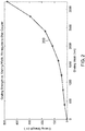
- Figure 2 is a graph of theoretical simulations of the grating strength as a function of grating width within a waveguide-to-slab coupler. As shown in the graph of Figure 2 , the grating strength can be controlled by changing the grating width. As the grating width is increased, such as from about 500-3000 nm, a corresponding increase in grating strength is produced as indicated by plot line 200.
- FIG. 3 is a schematic orthogonal view of a waveguide-to-slab coupler 300, according to another embodiment.
- the waveguide-to-slab coupler 300 comprises an input waveguide 310, a grating structure 320 on a portion of waveguide 310, and an output slab 330 that adjoins with one side of grating structure 320.
- the waveguide 310 has a first edge 312 and an opposing second edge 314 that extend in a direction substantially parallel to a propagation direction of an input light beam 340 injected into waveguide 310.
- the waveguide 310 has a waveguide width 316 between first edge 312 and second edge 314.
- the grating structure 320 is written on a portion of waveguide 310 adjacent to slab 330.
- the grating structure 320 includes an array of grating lines 322 that are angled with respect to the propagation direction of input light beam 340.
- the grating structure 320 has a first side 324 and an opposing second side 326, which extend in the same direction as first edge 312 and second edge 314 of waveguide 310.
- the grating structure 320 has a grating width 328 between first side 324 and second side 328.
- grating width 328 is substantially the same as waveguide width 316.
- the grating width can be varied to be less than the waveguide width, such as described previously.
- grating structure 320 is formed to have a first thickness, with waveguide 310 and slab 330 formed to have a second thickness that is less than the first thickness.
- the slab 330 adjoins with first side 324 of grating structure 320 such that slab 330 is in optical communication with an output of grating structure 320.
- the grating lines 322 are configured to diffract input light beam 340 into slab 330 at an angle with respect to the propagation direction of input light beam 340, such that a diffracted light beam 342 is output from slab 330.
- FIG. 4 illustrates schematic side views of a method for fabricating an optical coupler device such as a waveguide-to-slab coupler, according to one exemplary approach.
- a substrate layer 402 is provided such as an initial wafer, which has an upper surface 404.
- the substrate layer 402 can be a lower cladding layer and is composed of a lower refractive index material, such as silicon dioxide.
- the substrate layer 402 can also include an underlying handle wafer such as a silicon handle.
- the substrate layer 402 can be coupled to a silicon photonics chip.
- a guiding layer 412 is deposited on upper surface 404 of substrate layer 402, such as by a conventional deposition process.
- the guiding layer 412 includes a higher refractive index material, such as silicon nitride.
- a first resist spinning process is carried out to form a first resist layer 422 over guiding layer 412.
- a first resist development process is performed such as by lithography, to form an initial waveguide pattern that exposes portions of guiding layer 412.
- a first etching step is then carried out to remove the exposed portions of guiding layer 412 to form a waveguide layer 452 under first resist layer 422.
- the waveguide layer 452 includes an input waveguide portion that is coupled to one edge of a slab portion.
- a first resist removal process to remove first resist layer 422 and expose waveguide layer 452.
- a second resist spinning process is carried out to form a second resist layer 462 over waveguide layer 452 and an upper surface portion of substrate layer 402.
- a second resist development process is performed such as by lithography, to form a grating pattern that exposes portions of waveguide layer 452.
- a second etching step is then carried out to remove some of the material of waveguide layer 452 to form a grating 482 in a part of the input waveguide portion, and to reduce a thickness of the slab portion to form an output slab 484.
- This is followed in step 490 by a second resist removal process to remove second resist layer 462, such that the input waveguide portion, grating 482, and slab 484 form a waveguide-to-slab coupler.
- the waveguide-to-slab coupler is formed to have a substantially planar shape on substrate layer 402.
- the grating 482 can be formed to have a width that is the same as, or less than, a total width of the waveguide portion.
- an upper cladding layer 492 can be formed over the waveguide-to-slab coupler formed on substrate layer 402, such as by a conventional deposition process, to further protect the waveguide-to-slab coupler.
- the upper cladding layer 492 can include a lower refractive index material, such as silicon dioxide.
Landscapes
- Physics & Mathematics (AREA)
- General Physics & Mathematics (AREA)
- Optics & Photonics (AREA)
- Engineering & Computer Science (AREA)
- Microelectronics & Electronic Packaging (AREA)
- Manufacturing & Machinery (AREA)
- Optical Integrated Circuits (AREA)
Abstract
Description
- This invention was made with Government support under HR0011-16-C-0122 awarded by DARPA. The Government has certain rights in the invention.
- In integrated photonics it is often necessary to transition the spatial dimensions of a light wave from a highly confined waveguide state to a more broadly spatially distributed state compatible with free-space optics. An important field in which this functionality is desirable is the generation of free-space beams, derived from integrated photonics waveguides, for use with magneto-optic traps (MOTs).
- The most straightforward way to couple an integrated photonics waveguide mode into a wide slab mode is to direct a waveguide into a slab and allow the light to diverge naturally. There are, however, various shortcomings which are intrinsic to this approach. For instance, a significant amount of propagation is required to allow the light beam to diverge to any required size, and this can take up valuable real estate on the surface of the integrated photonics chip. Further, only a Gaussian profile may be realized in this manner, whereas a uniform intensity distribution is often more desirable. Additionally, the beam which this approach generates is diverging, whereas a collimated beam is often more needed to be generated.
- An optical coupler device comprises an optical waveguide having a first edge and an opposing second edge that extend in a direction substantially parallel to a propagation direction of an input light beam injected into the optical waveguide, with the optical waveguide having a waveguide width between the first and second edges. A grating structure is on a portion of the optical waveguide, with the grating structure having a first side and an opposing second side. The first and second sides of the grating structure extend in the same direction as the first and second edges of the optical waveguide, with the grating structure having a grating width between the first and second sides. An optical slab adjoins with the first side of the grating structure and is in optical communication with an output of the grating structure. The grating structure includes an array of grating lines that are angled with respect to the propagation direction of the input light beam. The grating lines are configured to diffract the input light beam into the optical slab at an angle with respect to the propagation direction of the input light beam, such that a diffracted light beam is output from the optical slab.
- Understanding that the drawings depict only exemplary embodiments and are not therefore to be considered limiting in scope, the exemplary embodiments will be described with additional specificity and detail through the use of the accompanying drawings, in which:
-
Figure 1 is a schematic top plan view of a waveguide-to-slab coupler according to one embodiment; -
Figure 2 is a graph of theoretical simulations of grating strength as a function of grating width within a waveguide-to-slab coupler; -
Figure 3 is a schematic orthogonal view of a waveguide-to-slab coupler, according to another embodiment; and -
Figure 4 shows schematic side views of a method for fabricating a waveguide-to-slab coupler, according to an exemplary approach. - In the following detailed description, embodiments are described in sufficient detail to enable those skilled in the art to practice the invention. It is to be understood that other embodiments may be utilized without departing from the scope of the invention. The following detailed description is, therefore, not to be taken in a limiting sense.
- An optical coupler device for the emission of arbitrary optical beam profiles from a waveguide into two-dimensional space is described herein. The optical coupler device can be implemented as a waveguide-to-slab coupler that is particularly suited to provide that a wide two-dimensional light wave be initially generated from an integrated photonics waveguide.
- In conventional optical devices used in integrated photonics, a waveguide is normally incident upon a slab. Such a configuration has several problems, including that the spatial expansion of the incident light beam is gradual, the light beam is diverging, and amplitude distribution of the light beam is fixed at a Gaussian. The present approach solves these problems by introducing a grating into a waveguide and positioning a slab to one side of the grating to produce a waveguide-to-slab coupler.
- A light beam propagating along the waveguide of the waveguide-to-slab coupler can be made to diffract off of the grating and into the slab at an angle, such as about 90 degrees. The grating strength can be modified by changing a width of the grating within the waveguide. By using a grating with a spatially dependent width, a light beam, propagating in the slab to the side of the waveguide, can be generated with any desired intensity distribution. Further, the light beam in this slab does not require any particular propagation length, for gradual expansion of the light beam, in contrast to prior techniques. In addition, the light beam output from the slab is collimated, rather than diverging, making the light beam more easily interfaced with out-of-plane grating couplers.
- To make the present optical coupler device, a waveguide can be formed on an integrated photonics chip through any number of established fabrication processes. Using the design of a first lithography mask, the process can direct the waveguide into one edge of a large slab. After applying this mask to a first round of lithography and etching, the process applies a second lithography mask to the sample. The process then etches a grating partially into the waveguide, and also etches partially into the slab. This results in a waveguide-to-slab coupler in which the waveguide couples light gradually into the slab through grating diffraction, such as at a 90 degree angle from its original direction of propagation, and at a controllable coupling rate, which is controllable via the grating width.
- The waveguide-to-slab coupler is particularly suited for use in an integrated photonics chip such as a silicon photonics chip, which is used in the generation of free space beams for a magneto-optic trap (MOT). Such a chip is designed to emit light beams at designed angles into free space, such as three expanded beams that intersect with each other in free space for use in a MOT. The waveguide-to-slab coupler takes input light from a single waveguide mode, and uses the grating to convert the input light into a slab mode of diffracted light in-plane, in which the diffracted light has a uniform amplitude and predetermined set width. This diffracted light can then be interfaced with out-of-plane grating couplers on the chip to produce the expanded beams that intersect with each other in free space.
- Further details of various embodiments are described hereafter with reference to the drawings.
-
Figure 1 is a schematic top plan view of an optical coupler device comprising a waveguide-to-slab coupler 100, according to one embodiment. The waveguide-to-slab coupler 100 includes asubstrate 110 having anupper surface 112, and an inputoptical waveguide 120 supported onupper surface 112 ofsubstrate 110. Thewaveguide 120 has afirst edge 122 and an opposingsecond edge 124 that extend in a direction substantially parallel to a propagation direction (x-axis) of aninput light beam 150 injected intowaveguide 120. Thewaveguide 120 has awaveguide width 126 having a first distance betweenfirst edge 122 andsecond edge 124. - A
grating structure 130 is formed on a portion ofwaveguide 120 so as to extend along a section ofwaveguide 120 adjacent tofirst edge 122. Thegrating structure 130 includes an array ofgrating lines 132 that are angled with respect to the propagation direction ofinput light beam 150. In this embodiment,grating structure 130 has agrating width 134 that is less than thewaveguide width 126. - An output
optical slab 140, supported bysubstrate 110,borders grating structure 130 alongfirst edge 122 and is in optical communication withgrating structure 130. Thewaveguide 120,grating structure 130, andslab 140 are substantially planar with respect to each other, such thatinput light beam 150 and a diffractedlight 152 beam propagate in substantially the same plane. - As discussed further hereafter,
grating structure 130 has a grating strength that is a function ofgrating width 134, such that the grating strength increases with an increase in the size ofgrating width 134. For example,grating width 134 can have a range of about 0.2 microns to about 10 microns. In addition, the size ratio ofgrating width 134 with respect towaveguide width 126 can be greater than 0 and up to 1. - In this embodiment,
waveguide 120 andgrating structure 130 can be formed to have a first thickness abovesubstrate 110, andslab 140 can be formed to have a second thickness that is less than the first thickness. Alternatively,waveguide 120 can be formed to have the same thickness asslab 140, such thatgrating structure 130 has a thickness greater than the thickness ofwaveguide 120 and slab 140. - The
substrate 110 can be a cladding layer and is composed of a lower refractive index material, such as silicon dioxide (SiO2), aluminum oxide (Al2O3), magnesium oxide (MgO), or potassium chloride (KCl). Thesubstrate layer 110 can be coupled onto an integrated photonics chip, such as a silicon photonics chip. - The
waveguide 120,grating structure 130, andslab 140 are composed of a higher refractive index material, such as silicon nitride (Si3N4), silicon (Si), titanium dioxide (TiO2), gallium arsenide (GaAs), or gallium nitride (GaN). - To operate waveguide-to-
slab coupler 100, inputlight beam 150 is injected from an optical source intowaveguide 120. Theinput light beam 150 propagates alongwaveguide 120 and is gradually diffracted by gratingstructure 130 intoslab 140 at about a 90 degree angle (y-axis) with respect to the propagation direction ofinput light beam 150. The diffractedlight beam 152, which is collimated, is then output fromslab 330. - The grating is designed to cancel out an x-component of the momentum of the light beam traveling along the x-axis, and to add a y-component to the momentum of the light beam, such that the light beam is diffracted to propagate along the y-axis. The grating produces a distributed effect, so the light beam gradually leaves the waveguide and enters the slab traveling in the same direction.
- The grating gradually and controllably diffracts light into the slab. The rate of diffraction can be controlled by changing the grating width relative to the waveguide width. The grating strength of the waveguide-to-slab coupler can be modified by changing the grating width within the waveguide. By using a grating with a spatially dependent width, the light beam, propagating through the slab, can be generated with any desired intensity distribution.
-
Figure 2 is a graph of theoretical simulations of the grating strength as a function of grating width within a waveguide-to-slab coupler. As shown in the graph ofFigure 2 , the grating strength can be controlled by changing the grating width. As the grating width is increased, such as from about 500-3000 nm, a corresponding increase in grating strength is produced as indicated byplot line 200. -
Figure 3 is a schematic orthogonal view of a waveguide-to-slab coupler 300, according to another embodiment. The waveguide-to-slab coupler 300 comprises aninput waveguide 310, a grating structure 320 on a portion ofwaveguide 310, and anoutput slab 330 that adjoins with one side of grating structure 320. - The
waveguide 310 has afirst edge 312 and an opposingsecond edge 314 that extend in a direction substantially parallel to a propagation direction of aninput light beam 340 injected intowaveguide 310. Thewaveguide 310 has awaveguide width 316 betweenfirst edge 312 andsecond edge 314. - The grating structure 320 is written on a portion of
waveguide 310 adjacent toslab 330. The grating structure 320 includes an array of gratinglines 322 that are angled with respect to the propagation direction ofinput light beam 340. The grating structure 320 has afirst side 324 and an opposing second side 326, which extend in the same direction asfirst edge 312 andsecond edge 314 ofwaveguide 310. - The grating structure 320 has a
grating width 328 betweenfirst side 324 andsecond side 328. In this embodiment, gratingwidth 328 is substantially the same aswaveguide width 316. In other embodiments, the grating width can be varied to be less than the waveguide width, such as described previously. - In this embodiment, grating structure 320 is formed to have a first thickness, with
waveguide 310 andslab 330 formed to have a second thickness that is less than the first thickness. - The
slab 330 adjoins withfirst side 324 of grating structure 320 such thatslab 330 is in optical communication with an output of grating structure 320. Thegrating lines 322 are configured to diffractinput light beam 340 intoslab 330 at an angle with respect to the propagation direction ofinput light beam 340, such that a diffractedlight beam 342 is output fromslab 330. -
Figure 4 illustrates schematic side views of a method for fabricating an optical coupler device such as a waveguide-to-slab coupler, according to one exemplary approach. Initially, as shown instep 400, asubstrate layer 402 is provided such as an initial wafer, which has anupper surface 404. Thesubstrate layer 402 can be a lower cladding layer and is composed of a lower refractive index material, such as silicon dioxide. Thesubstrate layer 402 can also include an underlying handle wafer such as a silicon handle. Thesubstrate layer 402 can be coupled to a silicon photonics chip. - As depicted in
step 410, aguiding layer 412 is deposited onupper surface 404 ofsubstrate layer 402, such as by a conventional deposition process. Theguiding layer 412 includes a higher refractive index material, such as silicon nitride. Next, as shown in step 420 a first resist spinning process is carried out to form a first resistlayer 422 over guidinglayer 412. Thereafter, as depicted instep 430, a first resist development process is performed such as by lithography, to form an initial waveguide pattern that exposes portions of guidinglayer 412. - As shown in
step 440, a first etching step is then carried out to remove the exposed portions of guidinglayer 412 to form awaveguide layer 452 under first resistlayer 422. Thewaveguide layer 452 includes an input waveguide portion that is coupled to one edge of a slab portion. This is followed instep 450 by a first resist removal process to remove first resistlayer 422 and exposewaveguide layer 452. Next, as shown instep 460, a second resist spinning process is carried out to form a second resistlayer 462 overwaveguide layer 452 and an upper surface portion ofsubstrate layer 402. - Thereafter, as depicted in
step 470, a second resist development process is performed such as by lithography, to form a grating pattern that exposes portions ofwaveguide layer 452. Next, as shown instep 480, a second etching step is then carried out to remove some of the material ofwaveguide layer 452 to form a grating 482 in a part of the input waveguide portion, and to reduce a thickness of the slab portion to form anoutput slab 484. This is followed in step 490 by a second resist removal process to remove second resistlayer 462, such that the input waveguide portion, grating 482, andslab 484 form a waveguide-to-slab coupler. - The waveguide-to-slab coupler is formed to have a substantially planar shape on
substrate layer 402. The grating 482 can be formed to have a width that is the same as, or less than, a total width of the waveguide portion. - Optionally, an
upper cladding layer 492 can be formed over the waveguide-to-slab coupler formed onsubstrate layer 402, such as by a conventional deposition process, to further protect the waveguide-to-slab coupler. Theupper cladding layer 492 can include a lower refractive index material, such as silicon dioxide. -
- Example 1 includes an optical coupler device, comprising: an optical waveguide having a first edge and an opposing second edge that extend in a direction substantially parallel to a propagation direction of an input light beam injected into the optical waveguide, the optical waveguide having a waveguide width between the first and second edges; a grating structure on a portion of the optical waveguide, the grating structure having a first side and an opposing second side, the first and second sides of the grating structure extending in the same direction as the first and second edges of the optical waveguide, the grating structure having a grating width between the first and second sides; and an optical slab that adjoins with the first side of the grating structure, the optical slab in optical communication with an output of the grating structure; wherein the grating structure includes an array of grating lines that are angled with respect to the propagation direction of the input light beam, the grating lines configured to diffract the input light beam into the optical slab at an angle with respect to the propagation direction of the input light beam, such that a diffracted light beam is output from the optical slab.
- Example 2 includes the optical coupler device of Example 1, wherein the optical waveguide, the grating structure, and the optical slab are substantially planar with respect to each other.
- Example 3 includes the optical coupler device of any of Examples claim 1-2, wherein the input light beam and the diffracted light beam propagate in substantially the same plane.
- Example 4 includes the optical coupler device of any of Examples 1-3, wherein the grating lines are configured to diffract the input light beam into the optical slab such that the diffracted light beam is output from the optical slab at about a 90 degree angle with respect to the propagation direction of the input light beam.
- Example 5 includes the optical coupler device of any of Examples 1-4, wherein the diffracted light beam output from the optical slab is a collimated beam.
- Example 6 includes the optical coupler device of any of Examples 1-5, wherein the grating structure has a grating strength that is a function of the grating width, such that the grating strength increases with an increase in the grating width.
- Example 7 includes the optical coupler device of any of Examples 1-6, wherein the grating width is same as, or less than, the waveguide width.
- Example 8 includes the optical coupler device of any of Examples 1-7, wherein the grating width has a range of about 0.2 microns to about 10 microns.
- Example 9 includes the optical coupler device of any of Examples 1-8, wherein a size ratio of the grating width with respect to the waveguide width is greater than 0 and up to about 1.
- Example 10 includes the optical coupler device of any of Examples 1-9, further comprising a substrate that supports the optical waveguide, the grating structure, and the optical slab.
- Example 11 includes the optical coupler device of Example 10, wherein the substrate comprises a first material having a first refractive index.
- Example 12 includes the optical coupler device of Example 11, wherein the optical waveguide, the grating structure, and the optical slab each comprise a second material having a second refractive index that is greater than the first refractive index.
- Example 13 includes the optical coupler device of Example 12, wherein the first material comprises silicon dioxide, and the second material comprises silicon nitride.
- Example 14 includes the optical coupler device of any of Examples 10-13, wherein the substrate is coupled to an integrated photonics chip.
- Example 15 includes a method of fabricating an optical coupler device, the method comprising: providing a substrate layer having an upper surface, the substrate layer including a first material having a first refractive index; depositing a guiding layer on the upper surface of the substrate layer, the guiding layer including a second material having a second refractive index that is greater than the first refractive index; forming a first resist layer over the guiding layer; forming an initial waveguide pattern that exposes portions of the guiding layer; etching the exposed portions of the guiding layer to form a waveguide layer, wherein the waveguide layer includes an input waveguide portion coupled to one edge of a slab portion; removing the first resist layer to expose the waveguide layer; forming a second resist layer over the waveguide layer; forming a grating pattern that exposes portions of the waveguide layer; etching the exposed portions of the waveguide layer to form a grating in part of the input waveguide portion, and to reduce a thickness of the slab portion to form an output slab; and removing the second resist layer such that the input waveguide portion, the grating, and the output slab, form a waveguide-to-slab coupler.
- Example 16 includes the method of Example 15, further comprising forming an upper cladding layer over the waveguide-to-slab coupler after removing the second resist layer, the upper cladding layer comprising the first material having the first refractive index.
- Example 17 includes the method of any of Examples 15-16, wherein the first material comprises silicon dioxide, and the second material comprises silicon nitride.
- Example 18 includes the method of any of Examples 15-17, wherein the waveguide-to-slab coupler is formed to have a substantially planar shape.
- Example 19 includes the method of any of Examples 15-18, wherein the grating is formed to have a width that is the same as, or less than, a total width of the waveguide portion.
- Example 20 includes the method of any of Examples 15-19, wherein the substrate layer is coupled to a silicon photonics chip.
- The present invention may be embodied in other specific forms without departing from its essential characteristics. The described embodiments are to be considered in all respects only as illustrative and not restrictive. The scope of the invention is therefore indicated by the appended claims rather than by the foregoing description. All changes that come within the meaning and range of equivalency of the claims are to be embraced within their scope.
Claims (10)
- An optical coupler device, comprising:an optical waveguide having a first edge and an opposing second edge that extend in a direction substantially parallel to a propagation direction of an input light beam injected into the optical waveguide, the optical waveguide having a waveguide width between the first and second edges;a grating structure on a portion of the optical waveguide, the grating structure having a first side and an opposing second side, the first and second sides of the grating structure extending in the same direction as the first and second edges of the optical waveguide, the grating structure having a grating width between the first and second sides; andan optical slab that adjoins with the first side of the grating structure, the optical slab in optical communication with an output of the grating structure;wherein the grating structure includes an array of grating lines that are angled with respect to the propagation direction of the input light beam, the grating lines configured to diffract the input light beam into the optical slab at an angle with respect to the propagation direction of the input light beam, such that a diffracted light beam is output from the optical slab.
- The optical coupler device of claim 1, wherein:the optical waveguide, the grating structure, and the optical slab are substantially planar with respect to each other; andthe input light beam and the diffracted light beam propagate in substantially the same plane.
- The optical coupler device of claim 2, wherein the grating lines are configured to diffract the input light beam into the optical slab such that the diffracted light beam is output from the optical slab at about a 90 degree angle with respect to the propagation direction of the input light beam.
- The optical coupler device of claim 1, wherein the grating structure has a grating strength that is a function of the grating width, such that the grating strength increases with an increase in the grating width.
- The optical coupler device of claim 1, wherein the grating width is same as, or less than, the waveguide width.
- The optical coupler device of claim 1, further comprising a substrate that supports the optical waveguide, the grating structure, and the optical slab.
- The optical coupler device of claim 6, wherein:the substrate comprises a first material having a first refractive index; andthe optical waveguide, the grating structure, and the optical slab each comprise a second material having a second refractive index that is greater than the first refractive index.
- The optical coupler device of claim 6, wherein the substrate is coupled to an integrated photonics chip.
- A method of fabricating an optical coupler device, the method comprising:providing a substrate layer having an upper surface, the substrate layer including a first material having a first refractive index;depositing a guiding layer on the upper surface of the substrate layer, the guiding layer including a second material having a second refractive index that is greater than the first refractive index;forming a first resist layer over the guiding layer;forming an initial waveguide pattern that exposes portions of the guiding layer;etching the exposed portions of the guiding layer to form a waveguide layer, wherein the waveguide layer includes an input waveguide portion coupled to one edge of a slab portion;removing the first resist layer to expose the waveguide layer;forming a second resist layer over the waveguide layer;forming a grating pattern that exposes portions of the waveguide layer;etching the exposed portions of the waveguide layer to form a grating in part of the input waveguide portion, and to reduce a thickness of the slab portion to form an output slab; andremoving the second resist layer such that the input waveguide portion, the grating, and the output slab, form a waveguide-to-slab coupler.
- The method of claim 9, further comprising:
forming an upper cladding layer over the waveguide-to-slab coupler after removing the second resist layer, the upper cladding layer comprising the first material having the first refractive index.
Applications Claiming Priority (1)
| Application Number | Priority Date | Filing Date | Title |
|---|---|---|---|
| US16/803,712 US11105977B1 (en) | 2020-02-27 | 2020-02-27 | Device for the emission of arbitrary optical beam profiles from waveguides into two-dimensional space |
Publications (2)
| Publication Number | Publication Date |
|---|---|
| EP3872542A1 true EP3872542A1 (en) | 2021-09-01 |
| EP3872542B1 EP3872542B1 (en) | 2022-03-09 |
Family
ID=73790027
Family Applications (1)
| Application Number | Title | Priority Date | Filing Date |
|---|---|---|---|
| EP20212909.4A Active EP3872542B1 (en) | 2020-02-27 | 2020-12-09 | Device for the emission of arbitrary optical beam profiles from waveguides into two-dimensional space |
Country Status (2)
| Country | Link |
|---|---|
| US (1) | US11105977B1 (en) |
| EP (1) | EP3872542B1 (en) |
Families Citing this family (2)
| Publication number | Priority date | Publication date | Assignee | Title |
|---|---|---|---|---|
| US11567266B1 (en) * | 2021-12-15 | 2023-01-31 | Globalfoundries U.S. Inc. | Angled grating couplers with inclined side edge portions |
| WO2025030421A1 (en) * | 2023-08-09 | 2025-02-13 | 深圳力策科技有限公司 | Acousto-optic beam control chip and manufacturing method therefor |
Citations (5)
| Publication number | Priority date | Publication date | Assignee | Title |
|---|---|---|---|---|
| US4776661A (en) * | 1985-11-25 | 1988-10-11 | Canon Kabushiki Kaisha | Integrated optical device |
| EP0325251A2 (en) * | 1988-01-20 | 1989-07-26 | Canon Kabushiki Kaisha | Laser light source for generating beam collimated in at least one direction |
| EP1338906A1 (en) * | 2002-02-21 | 2003-08-27 | Trw Inc. | Integrated waveguide frequency router |
| US20040208444A1 (en) * | 2002-06-04 | 2004-10-21 | Anders Grunnet-Jepsen | Method and apparatus for monitoring optical signals in a planar lightwave circuit via in-plane filtering |
| US7720334B1 (en) * | 2006-07-07 | 2010-05-18 | Mossberg Thomas W | Laterally-confined holographic spectral filters |
Family Cites Families (9)
| Publication number | Priority date | Publication date | Assignee | Title |
|---|---|---|---|---|
| US5226100A (en) | 1990-09-21 | 1993-07-06 | Siemens Aktiengesellschaft | Optical grating comprising a plurality of side-by-side outfeed end faces of optical waveguides |
| US6493487B1 (en) | 2000-07-14 | 2002-12-10 | Applied Wdm, Inc. | Optical waveguide transmission devices |
| EP1653260A1 (en) | 2003-07-18 | 2006-05-03 | Nippon Sheet Glass Co.,Ltd. | Photonic crystal waveguide, homogeneous medium waveguide, and optical device |
| EP1743197B1 (en) | 2004-04-23 | 2011-08-10 | Olivier M. Parriaux | High efficiency optical diffraction device |
| US7327924B2 (en) | 2004-09-23 | 2008-02-05 | Stc.Unm | Generalized transverse bragg waveguide |
| JP4429323B2 (en) | 2005-01-18 | 2010-03-10 | 日本板硝子株式会社 | Waveguide element, method for manufacturing waveguide element, and optical sensor |
| US10613281B2 (en) | 2008-07-09 | 2020-04-07 | Luxtera, Inc. | Method and system for coupling a light source assembly to an optical integrated circuit |
| GB201115784D0 (en) | 2011-09-13 | 2011-10-26 | Univ Gent | Integrated photonics waveguide grating coupler |
| US9753219B2 (en) | 2015-02-13 | 2017-09-05 | Clarkson University | Optical coupler with forked grating structure |
-
2020
- 2020-02-27 US US16/803,712 patent/US11105977B1/en active Active
- 2020-12-09 EP EP20212909.4A patent/EP3872542B1/en active Active
Patent Citations (5)
| Publication number | Priority date | Publication date | Assignee | Title |
|---|---|---|---|---|
| US4776661A (en) * | 1985-11-25 | 1988-10-11 | Canon Kabushiki Kaisha | Integrated optical device |
| EP0325251A2 (en) * | 1988-01-20 | 1989-07-26 | Canon Kabushiki Kaisha | Laser light source for generating beam collimated in at least one direction |
| EP1338906A1 (en) * | 2002-02-21 | 2003-08-27 | Trw Inc. | Integrated waveguide frequency router |
| US20040208444A1 (en) * | 2002-06-04 | 2004-10-21 | Anders Grunnet-Jepsen | Method and apparatus for monitoring optical signals in a planar lightwave circuit via in-plane filtering |
| US7720334B1 (en) * | 2006-07-07 | 2010-05-18 | Mossberg Thomas W | Laterally-confined holographic spectral filters |
Also Published As
| Publication number | Publication date |
|---|---|
| US11105977B1 (en) | 2021-08-31 |
| US20210271021A1 (en) | 2021-09-02 |
| EP3872542B1 (en) | 2022-03-09 |
Similar Documents
| Publication | Publication Date | Title |
|---|---|---|
| EP1606660B1 (en) | Polarization splitting grating couplers | |
| JP4278597B2 (en) | Light control element | |
| EP1255135B1 (en) | Two-dimensional photonic crystal slab and manufacturing method | |
| JP4208754B2 (en) | Optical delay element | |
| JP6069439B1 (en) | Polarization identification element | |
| CN113777708A (en) | analog converter | |
| EP2506048B1 (en) | Planar lightwave circuit, including an improved arrayed waveguide grating filter. | |
| US20090180731A1 (en) | Photonic coupler | |
| US8965157B2 (en) | Semiconductor pointed structure and method for fabricating same, spot size converter, and non-reflective terminator | |
| US20160238787A1 (en) | Forked grating coupler | |
| US11105977B1 (en) | Device for the emission of arbitrary optical beam profiles from waveguides into two-dimensional space | |
| US11215760B2 (en) | Device for emission of arbitrary optical beam profiles from a chip to free space | |
| JP3946879B2 (en) | Photonic crystal material | |
| Samanta et al. | A 1× 2 polarization-independent power splitter using three-coupled silicon rib waveguides | |
| Tandon et al. | The superprism effect using large area 2D-periodic photonic crystal slabs | |
| US12321011B2 (en) | Turning grating device for emission of arbitrary optical beam profiles from waveguides into two-dimensional space | |
| JP7577241B1 (en) | How Optical Devices Work | |
| US6944368B2 (en) | Waveguide-to-semiconductor device coupler | |
| US20240255768A1 (en) | Microlens devices to control far-field emission of a diverging planar beam | |
| Shinya et al. | Single-mode transmission in commensurate width-varied line-defect SOI photonic crystal waveguides | |
| WO2025013119A1 (en) | Optical device | |
| Sakin et al. | Ultracompact Tapers & Splitter for Fishbone-Like Grating Waveguides | |
| Chen et al. | One-Dimensional Grating Coupler on Thin Film Lithium Niobate for High-Efficiency and Polarization-Independent Coupling | |
| Watanabe et al. | Si wire waveguide devices | |
| Tokushima et al. | Pillar photonic crystal waveguides for integrated optical buffers |
Legal Events
| Date | Code | Title | Description |
|---|---|---|---|
| PUAI | Public reference made under article 153(3) epc to a published international application that has entered the european phase |
Free format text: ORIGINAL CODE: 0009012 |
|
| STAA | Information on the status of an ep patent application or granted ep patent |
Free format text: STATUS: REQUEST FOR EXAMINATION WAS MADE |
|
| 17P | Request for examination filed |
Effective date: 20210609 |
|
| AK | Designated contracting states |
Kind code of ref document: A1 Designated state(s): AL AT BE BG CH CY CZ DE DK EE ES FI FR GB GR HR HU IE IS IT LI LT LU LV MC MK MT NL NO PL PT RO RS SE SI SK SM TR |
|
| RIC1 | Information provided on ipc code assigned before grant |
Ipc: G21K 1/00 20060101ALN20210830BHEP Ipc: G02B 6/293 20060101ALN20210830BHEP Ipc: G02B 6/12 20060101ALN20210830BHEP Ipc: G02B 6/42 20060101ALI20210830BHEP Ipc: G02B 6/34 20060101ALI20210830BHEP Ipc: G02B 6/136 20060101ALI20210830BHEP Ipc: G02B 6/132 20060101ALI20210830BHEP Ipc: G02B 6/124 20060101AFI20210830BHEP |
|
| GRAP | Despatch of communication of intention to grant a patent |
Free format text: ORIGINAL CODE: EPIDOSNIGR1 |
|
| STAA | Information on the status of an ep patent application or granted ep patent |
Free format text: STATUS: GRANT OF PATENT IS INTENDED |
|
| RIC1 | Information provided on ipc code assigned before grant |
Ipc: G21K 1/00 20060101ALN20211004BHEP Ipc: G02B 6/293 20060101ALN20211004BHEP Ipc: G02B 6/12 20060101ALN20211004BHEP Ipc: G02B 6/42 20060101ALI20211004BHEP Ipc: G02B 6/34 20060101ALI20211004BHEP Ipc: G02B 6/136 20060101ALI20211004BHEP Ipc: G02B 6/132 20060101ALI20211004BHEP Ipc: G02B 6/124 20060101AFI20211004BHEP |
|
| INTG | Intention to grant announced |
Effective date: 20211021 |
|
| GRAS | Grant fee paid |
Free format text: ORIGINAL CODE: EPIDOSNIGR3 |
|
| GRAA | (expected) grant |
Free format text: ORIGINAL CODE: 0009210 |
|
| STAA | Information on the status of an ep patent application or granted ep patent |
Free format text: STATUS: THE PATENT HAS BEEN GRANTED |
|
| AK | Designated contracting states |
Kind code of ref document: B1 Designated state(s): AL AT BE BG CH CY CZ DE DK EE ES FI FR GB GR HR HU IE IS IT LI LT LU LV MC MK MT NL NO PL PT RO RS SE SI SK SM TR |
|
| REG | Reference to a national code |
Ref country code: CH Ref legal event code: EP Ref country code: AT Ref legal event code: REF Ref document number: 1474641 Country of ref document: AT Kind code of ref document: T Effective date: 20220315 |
|
| REG | Reference to a national code |
Ref country code: IE Ref legal event code: FG4D |
|
| REG | Reference to a national code |
Ref country code: DE Ref legal event code: R096 Ref document number: 602020002162 Country of ref document: DE |
|
| REG | Reference to a national code |
Ref country code: LT Ref legal event code: MG9D |
|
| REG | Reference to a national code |
Ref country code: NL Ref legal event code: MP Effective date: 20220309 |
|
| PG25 | Lapsed in a contracting state [announced via postgrant information from national office to epo] |
Ref country code: SE Free format text: LAPSE BECAUSE OF FAILURE TO SUBMIT A TRANSLATION OF THE DESCRIPTION OR TO PAY THE FEE WITHIN THE PRESCRIBED TIME-LIMIT Effective date: 20220309 Ref country code: RS Free format text: LAPSE BECAUSE OF FAILURE TO SUBMIT A TRANSLATION OF THE DESCRIPTION OR TO PAY THE FEE WITHIN THE PRESCRIBED TIME-LIMIT Effective date: 20220309 Ref country code: NO Free format text: LAPSE BECAUSE OF FAILURE TO SUBMIT A TRANSLATION OF THE DESCRIPTION OR TO PAY THE FEE WITHIN THE PRESCRIBED TIME-LIMIT Effective date: 20220609 Ref country code: LT Free format text: LAPSE BECAUSE OF FAILURE TO SUBMIT A TRANSLATION OF THE DESCRIPTION OR TO PAY THE FEE WITHIN THE PRESCRIBED TIME-LIMIT Effective date: 20220309 Ref country code: HR Free format text: LAPSE BECAUSE OF FAILURE TO SUBMIT A TRANSLATION OF THE DESCRIPTION OR TO PAY THE FEE WITHIN THE PRESCRIBED TIME-LIMIT Effective date: 20220309 Ref country code: BG Free format text: LAPSE BECAUSE OF FAILURE TO SUBMIT A TRANSLATION OF THE DESCRIPTION OR TO PAY THE FEE WITHIN THE PRESCRIBED TIME-LIMIT Effective date: 20220609 |
|
| REG | Reference to a national code |
Ref country code: AT Ref legal event code: MK05 Ref document number: 1474641 Country of ref document: AT Kind code of ref document: T Effective date: 20220309 |
|
| PG25 | Lapsed in a contracting state [announced via postgrant information from national office to epo] |
Ref country code: LV Free format text: LAPSE BECAUSE OF FAILURE TO SUBMIT A TRANSLATION OF THE DESCRIPTION OR TO PAY THE FEE WITHIN THE PRESCRIBED TIME-LIMIT Effective date: 20220309 Ref country code: GR Free format text: LAPSE BECAUSE OF FAILURE TO SUBMIT A TRANSLATION OF THE DESCRIPTION OR TO PAY THE FEE WITHIN THE PRESCRIBED TIME-LIMIT Effective date: 20220610 Ref country code: FI Free format text: LAPSE BECAUSE OF FAILURE TO SUBMIT A TRANSLATION OF THE DESCRIPTION OR TO PAY THE FEE WITHIN THE PRESCRIBED TIME-LIMIT Effective date: 20220309 |
|
| PG25 | Lapsed in a contracting state [announced via postgrant information from national office to epo] |
Ref country code: NL Free format text: LAPSE BECAUSE OF FAILURE TO SUBMIT A TRANSLATION OF THE DESCRIPTION OR TO PAY THE FEE WITHIN THE PRESCRIBED TIME-LIMIT Effective date: 20220309 |
|
| PG25 | Lapsed in a contracting state [announced via postgrant information from national office to epo] |
Ref country code: SM Free format text: LAPSE BECAUSE OF FAILURE TO SUBMIT A TRANSLATION OF THE DESCRIPTION OR TO PAY THE FEE WITHIN THE PRESCRIBED TIME-LIMIT Effective date: 20220309 Ref country code: SK Free format text: LAPSE BECAUSE OF FAILURE TO SUBMIT A TRANSLATION OF THE DESCRIPTION OR TO PAY THE FEE WITHIN THE PRESCRIBED TIME-LIMIT Effective date: 20220309 Ref country code: RO Free format text: LAPSE BECAUSE OF FAILURE TO SUBMIT A TRANSLATION OF THE DESCRIPTION OR TO PAY THE FEE WITHIN THE PRESCRIBED TIME-LIMIT Effective date: 20220309 Ref country code: PT Free format text: LAPSE BECAUSE OF FAILURE TO SUBMIT A TRANSLATION OF THE DESCRIPTION OR TO PAY THE FEE WITHIN THE PRESCRIBED TIME-LIMIT Effective date: 20220711 Ref country code: ES Free format text: LAPSE BECAUSE OF FAILURE TO SUBMIT A TRANSLATION OF THE DESCRIPTION OR TO PAY THE FEE WITHIN THE PRESCRIBED TIME-LIMIT Effective date: 20220309 Ref country code: EE Free format text: LAPSE BECAUSE OF FAILURE TO SUBMIT A TRANSLATION OF THE DESCRIPTION OR TO PAY THE FEE WITHIN THE PRESCRIBED TIME-LIMIT Effective date: 20220309 Ref country code: CZ Free format text: LAPSE BECAUSE OF FAILURE TO SUBMIT A TRANSLATION OF THE DESCRIPTION OR TO PAY THE FEE WITHIN THE PRESCRIBED TIME-LIMIT Effective date: 20220309 Ref country code: AT Free format text: LAPSE BECAUSE OF FAILURE TO SUBMIT A TRANSLATION OF THE DESCRIPTION OR TO PAY THE FEE WITHIN THE PRESCRIBED TIME-LIMIT Effective date: 20220309 |
|
| PG25 | Lapsed in a contracting state [announced via postgrant information from national office to epo] |
Ref country code: PL Free format text: LAPSE BECAUSE OF FAILURE TO SUBMIT A TRANSLATION OF THE DESCRIPTION OR TO PAY THE FEE WITHIN THE PRESCRIBED TIME-LIMIT Effective date: 20220309 Ref country code: IS Free format text: LAPSE BECAUSE OF FAILURE TO SUBMIT A TRANSLATION OF THE DESCRIPTION OR TO PAY THE FEE WITHIN THE PRESCRIBED TIME-LIMIT Effective date: 20220709 Ref country code: AL Free format text: LAPSE BECAUSE OF FAILURE TO SUBMIT A TRANSLATION OF THE DESCRIPTION OR TO PAY THE FEE WITHIN THE PRESCRIBED TIME-LIMIT Effective date: 20220309 |
|
| REG | Reference to a national code |
Ref country code: DE Ref legal event code: R097 Ref document number: 602020002162 Country of ref document: DE |
|
| PLBE | No opposition filed within time limit |
Free format text: ORIGINAL CODE: 0009261 |
|
| STAA | Information on the status of an ep patent application or granted ep patent |
Free format text: STATUS: NO OPPOSITION FILED WITHIN TIME LIMIT |
|
| PG25 | Lapsed in a contracting state [announced via postgrant information from national office to epo] |
Ref country code: DK Free format text: LAPSE BECAUSE OF FAILURE TO SUBMIT A TRANSLATION OF THE DESCRIPTION OR TO PAY THE FEE WITHIN THE PRESCRIBED TIME-LIMIT Effective date: 20220309 |
|
| 26N | No opposition filed |
Effective date: 20221212 |
|
| REG | Reference to a national code |
Ref country code: DE Ref legal event code: R119 Ref document number: 602020002162 Country of ref document: DE |
|
| P01 | Opt-out of the competence of the unified patent court (upc) registered |
Effective date: 20230525 |
|
| PG25 | Lapsed in a contracting state [announced via postgrant information from national office to epo] |
Ref country code: IT Free format text: LAPSE BECAUSE OF FAILURE TO SUBMIT A TRANSLATION OF THE DESCRIPTION OR TO PAY THE FEE WITHIN THE PRESCRIBED TIME-LIMIT Effective date: 20220309 |
|
| REG | Reference to a national code |
Ref country code: BE Ref legal event code: MM Effective date: 20221231 |
|
| PG25 | Lapsed in a contracting state [announced via postgrant information from national office to epo] |
Ref country code: LU Free format text: LAPSE BECAUSE OF NON-PAYMENT OF DUE FEES Effective date: 20221209 |
|
| PG25 | Lapsed in a contracting state [announced via postgrant information from national office to epo] |
Ref country code: IE Free format text: LAPSE BECAUSE OF NON-PAYMENT OF DUE FEES Effective date: 20221209 Ref country code: DE Free format text: LAPSE BECAUSE OF NON-PAYMENT OF DUE FEES Effective date: 20230701 |
|
| PG25 | Lapsed in a contracting state [announced via postgrant information from national office to epo] |
Ref country code: BE Free format text: LAPSE BECAUSE OF NON-PAYMENT OF DUE FEES Effective date: 20221231 |
|
| PG25 | Lapsed in a contracting state [announced via postgrant information from national office to epo] |
Ref country code: CY Free format text: LAPSE BECAUSE OF FAILURE TO SUBMIT A TRANSLATION OF THE DESCRIPTION OR TO PAY THE FEE WITHIN THE PRESCRIBED TIME-LIMIT Effective date: 20220309 |
|
| PG25 | Lapsed in a contracting state [announced via postgrant information from national office to epo] |
Ref country code: MK Free format text: LAPSE BECAUSE OF FAILURE TO SUBMIT A TRANSLATION OF THE DESCRIPTION OR TO PAY THE FEE WITHIN THE PRESCRIBED TIME-LIMIT Effective date: 20220309 |
|
| PG25 | Lapsed in a contracting state [announced via postgrant information from national office to epo] |
Ref country code: MC Free format text: LAPSE BECAUSE OF FAILURE TO SUBMIT A TRANSLATION OF THE DESCRIPTION OR TO PAY THE FEE WITHIN THE PRESCRIBED TIME-LIMIT Effective date: 20220309 |
|
| PG25 | Lapsed in a contracting state [announced via postgrant information from national office to epo] |
Ref country code: MC Free format text: LAPSE BECAUSE OF FAILURE TO SUBMIT A TRANSLATION OF THE DESCRIPTION OR TO PAY THE FEE WITHIN THE PRESCRIBED TIME-LIMIT Effective date: 20220309 |
|
| PG25 | Lapsed in a contracting state [announced via postgrant information from national office to epo] |
Ref country code: MT Free format text: LAPSE BECAUSE OF FAILURE TO SUBMIT A TRANSLATION OF THE DESCRIPTION OR TO PAY THE FEE WITHIN THE PRESCRIBED TIME-LIMIT Effective date: 20220309 |
|
| PG25 | Lapsed in a contracting state [announced via postgrant information from national office to epo] |
Ref country code: HU Free format text: LAPSE BECAUSE OF FAILURE TO SUBMIT A TRANSLATION OF THE DESCRIPTION OR TO PAY THE FEE WITHIN THE PRESCRIBED TIME-LIMIT; INVALID AB INITIO Effective date: 20201209 |
|
| GBPC | Gb: european patent ceased through non-payment of renewal fee |
Effective date: 20241209 |
|
| PG25 | Lapsed in a contracting state [announced via postgrant information from national office to epo] |
Ref country code: GB Free format text: LAPSE BECAUSE OF NON-PAYMENT OF DUE FEES Effective date: 20241209 |
|
| PG25 | Lapsed in a contracting state [announced via postgrant information from national office to epo] |
Ref country code: TR Free format text: LAPSE BECAUSE OF FAILURE TO SUBMIT A TRANSLATION OF THE DESCRIPTION OR TO PAY THE FEE WITHIN THE PRESCRIBED TIME-LIMIT Effective date: 20220309 |
|
| REG | Reference to a national code |
Ref country code: CH Ref legal event code: U11 Free format text: ST27 STATUS EVENT CODE: U-0-0-U10-U11 (AS PROVIDED BY THE NATIONAL OFFICE) Effective date: 20260101 |
|
| PGFP | Annual fee paid to national office [announced via postgrant information from national office to epo] |
Ref country code: FR Payment date: 20251223 Year of fee payment: 6 |
|
| PG25 | Lapsed in a contracting state [announced via postgrant information from national office to epo] |
Ref country code: SI Free format text: LAPSE BECAUSE OF FAILURE TO SUBMIT A TRANSLATION OF THE DESCRIPTION OR TO PAY THE FEE WITHIN THE PRESCRIBED TIME-LIMIT Effective date: 20220309 |
|
| PGFP | Annual fee paid to national office [announced via postgrant information from national office to epo] |
Ref country code: CH Payment date: 20260101 Year of fee payment: 6 |