EP3872472A1 - Semiconductor device for ambient sensing including a cavity and corresponding manufacturing process. - Google Patents
Semiconductor device for ambient sensing including a cavity and corresponding manufacturing process. Download PDFInfo
- Publication number
- EP3872472A1 EP3872472A1 EP21159179.7A EP21159179A EP3872472A1 EP 3872472 A1 EP3872472 A1 EP 3872472A1 EP 21159179 A EP21159179 A EP 21159179A EP 3872472 A1 EP3872472 A1 EP 3872472A1
- Authority
- EP
- European Patent Office
- Prior art keywords
- hole
- cap
- channel
- region
- semiconductor device
- Prior art date
- Legal status (The legal status is an assumption and is not a legal conclusion. Google has not performed a legal analysis and makes no representation as to the accuracy of the status listed.)
- Granted
Links
Images




Classifications
-
- G—PHYSICS
- G01—MEASURING; TESTING
- G01L—MEASURING FORCE, STRESS, TORQUE, WORK, MECHANICAL POWER, MECHANICAL EFFICIENCY, OR FLUID PRESSURE
- G01L19/00—Details of, or accessories for, apparatus for measuring steady or quasi-steady pressure of a fluent medium insofar as such details or accessories are not special to particular types of pressure gauges
- G01L19/06—Means for preventing overload or deleterious influence of the measured medium on the measuring device or vice versa
- G01L19/0627—Protection against aggressive medium in general
- G01L19/0636—Protection against aggressive medium in general using particle filters
-
- G—PHYSICS
- G01—MEASURING; TESTING
- G01L—MEASURING FORCE, STRESS, TORQUE, WORK, MECHANICAL POWER, MECHANICAL EFFICIENCY, OR FLUID PRESSURE
- G01L9/00—Measuring steady of quasi-steady pressure of fluid or fluent solid material by electric or magnetic pressure-sensitive elements; Transmitting or indicating the displacement of mechanical pressure-sensitive elements, used to measure the steady or quasi-steady pressure of a fluid or fluent solid material, by electric or magnetic means
- G01L9/0041—Transmitting or indicating the displacement of flexible diaphragms
- G01L9/0042—Constructional details associated with semiconductive diaphragm sensors, e.g. etching, or constructional details of non-semiconductive diaphragms
-
- G—PHYSICS
- G01—MEASURING; TESTING
- G01L—MEASURING FORCE, STRESS, TORQUE, WORK, MECHANICAL POWER, MECHANICAL EFFICIENCY, OR FLUID PRESSURE
- G01L9/00—Measuring steady of quasi-steady pressure of fluid or fluent solid material by electric or magnetic pressure-sensitive elements; Transmitting or indicating the displacement of mechanical pressure-sensitive elements, used to measure the steady or quasi-steady pressure of a fluid or fluent solid material, by electric or magnetic means
- G01L9/0041—Transmitting or indicating the displacement of flexible diaphragms
- G01L9/0051—Transmitting or indicating the displacement of flexible diaphragms using variations in ohmic resistance
-
- G—PHYSICS
- G01—MEASURING; TESTING
- G01L—MEASURING FORCE, STRESS, TORQUE, WORK, MECHANICAL POWER, MECHANICAL EFFICIENCY, OR FLUID PRESSURE
- G01L9/00—Measuring steady of quasi-steady pressure of fluid or fluent solid material by electric or magnetic pressure-sensitive elements; Transmitting or indicating the displacement of mechanical pressure-sensitive elements, used to measure the steady or quasi-steady pressure of a fluid or fluent solid material, by electric or magnetic means
- G01L9/0041—Transmitting or indicating the displacement of flexible diaphragms
- G01L9/0072—Transmitting or indicating the displacement of flexible diaphragms using variations in capacitance
- G01L9/0073—Transmitting or indicating the displacement of flexible diaphragms using variations in capacitance using a semiconductive diaphragm
-
- G—PHYSICS
- G01—MEASURING; TESTING
- G01L—MEASURING FORCE, STRESS, TORQUE, WORK, MECHANICAL POWER, MECHANICAL EFFICIENCY, OR FLUID PRESSURE
- G01L9/00—Measuring steady of quasi-steady pressure of fluid or fluent solid material by electric or magnetic pressure-sensitive elements; Transmitting or indicating the displacement of mechanical pressure-sensitive elements, used to measure the steady or quasi-steady pressure of a fluid or fluent solid material, by electric or magnetic means
- G01L9/0041—Transmitting or indicating the displacement of flexible diaphragms
- G01L9/008—Transmitting or indicating the displacement of flexible diaphragms using piezoelectric devices
-
- G—PHYSICS
- G01—MEASURING; TESTING
- G01L—MEASURING FORCE, STRESS, TORQUE, WORK, MECHANICAL POWER, MECHANICAL EFFICIENCY, OR FLUID PRESSURE
- G01L9/00—Measuring steady of quasi-steady pressure of fluid or fluent solid material by electric or magnetic pressure-sensitive elements; Transmitting or indicating the displacement of mechanical pressure-sensitive elements, used to measure the steady or quasi-steady pressure of a fluid or fluent solid material, by electric or magnetic means
- G01L9/08—Measuring steady of quasi-steady pressure of fluid or fluent solid material by electric or magnetic pressure-sensitive elements; Transmitting or indicating the displacement of mechanical pressure-sensitive elements, used to measure the steady or quasi-steady pressure of a fluid or fluent solid material, by electric or magnetic means by making use of piezoelectric devices, i.e. electric circuits therefor
-
- G—PHYSICS
- G01—MEASURING; TESTING
- G01L—MEASURING FORCE, STRESS, TORQUE, WORK, MECHANICAL POWER, MECHANICAL EFFICIENCY, OR FLUID PRESSURE
- G01L9/00—Measuring steady of quasi-steady pressure of fluid or fluent solid material by electric or magnetic pressure-sensitive elements; Transmitting or indicating the displacement of mechanical pressure-sensitive elements, used to measure the steady or quasi-steady pressure of a fluid or fluent solid material, by electric or magnetic means
- G01L9/12—Measuring steady of quasi-steady pressure of fluid or fluent solid material by electric or magnetic pressure-sensitive elements; Transmitting or indicating the displacement of mechanical pressure-sensitive elements, used to measure the steady or quasi-steady pressure of a fluid or fluent solid material, by electric or magnetic means by making use of variations in capacitance, i.e. electric circuits therefor
Definitions
- the present invention relates to a semiconductor device for ambient sensing, which includes a cavity that can be coupled to the external world and a mechanical filtering structure; moreover, the present invention regards a corresponding manufacturing process.
- ambient sensors As is known, numerous sensors known as ambient sensors are currently available, which supply electrical signals representing parameters of the environment in which they are positioned, such as for example pressure, temperature, humidity, presence of gas etc. Inter alia, semiconductor devices that function as ambient sensors are known.
- Figure 1 shows a portion of a section of a sensing device 1 that comprises a semiconductor body 2, which in turn comprises a substrate 3, made, for example, of silicon, and an overlying epitaxial region 4, formed by one or more epitaxial layers and defining a first surface S 4 , which delimits the semiconductor body 2 at the top.
- a semiconductor body 2 which in turn comprises a substrate 3, made, for example, of silicon, and an overlying epitaxial region 4, formed by one or more epitaxial layers and defining a first surface S 4 , which delimits the semiconductor body 2 at the top.
- the sensing device 1 further comprises a first passivation layer 6, formed by a dielectric material (for example, oxide) and arranged on the first surface S 4 , and a second passivation layer 8, formed by a dielectric material (for example, nitride) and arranged on the first passivation layer 6.
- a first passivation layer 6 formed by a dielectric material (for example, oxide) and arranged on the first surface S 4
- a second passivation layer 8 formed by a dielectric material (for example, nitride) and arranged on the first passivation layer 6.
- the sensing device 1 further comprises a plurality of metallizations, which extend in the region formed by the first and second passivation layers 6, 8. For instance, a first bottom metallization 10 and a first top metallization 12, which are made of metal material, are visible in Figure 1 .
- the first bottom metallization 10 is arranged on the first surface S 4 , in contact with the epitaxial region 4, and is overlaid by the first passivation layer 6.
- the first top metallization 12 is arranged on the first passivation layer 6 and overlies, at a distance, the first bottom metallization 10.
- the second passivation layer 8 in part overlies the first top metallization 12.
- the second passivation layer 8 extends over the first top metallization 12 so as to leave a part of the latter exposed, i.e., so as to define a window 14 that faces the exposed part of the first top metallization 12, referred to in what follows as the sealing window 14.
- the sensing device 1 further comprises an active area 15, which typically extends from the first surface S 4 , within an underlying portion of the epitaxial region 4 and within a substrate portion 3 underlying the latter.
- the active area 15 is coated with the first and second passivation layers 6, 8 and is typically laterally staggered with respect to the metallizations.
- the active area 15 may be electrically connected to the first bottom metallization 10 and/or to further electrical terminals (not illustrated), which are designed to enable the electrical connection to the external world.
- the first top metallization 12 may have an electrical function (for example, it may be connected to the ground of the sensing device 1) or may be without any electrical function.
- the semiconductor body 2 and the first and second passivation layers 6, 8 form a main body 17 of the sensing device 1, which is delimited at the top by a second surface S 17 , formed by the second passivation layer 8.
- the sensing device 1 further comprises a cap 18 formed by semiconductor material (for example, silicon), which overlies, at a distance, the main body 17, so as to delimit a cavity 20.
- the cap 18 comprises a respective primary body 19, which has a planar shape and is delimited at the bottom by a third surface S 18 , and a projecting region 22, which extends downwards, starting from the third surface S 18 , in the direction of the main body 17.
- the projecting region 22 has a closed and hollow shape (for example, the shape of an annulus or of a rectangular frame) and is arranged so that, in top view (not illustrated), it surrounds the active area 15.
- the projecting region 22 forms a single piece with the primary body 19 of the cap 18.
- the projection 22 has an annular shape and has, in top view, the shape of an annulus, it includes a first and a second side wall P 11 , P 12 , which define cylindrical profiles, and a bottom wall P b .
- the sensing device 1 further comprises a junction region 23, which is formed, for example, by a germanium-aluminium eutectic alloy and extends underneath the bottom wall P b of the projection 22, with which it is in direct contact, until it penetrates partially within the first top metallization 12.
- junction region 23 extends within the sealing window 14, in contact with the underlying first top metallization 12 so as to function as junction between cap 18 and main body 17.
- junction region 23 and the first top metallization 12 are ring-shaped; i.e., they have shapes that are closed, in top view, and are hollow.
- the projecting region 22, the junction region 23 and the first top metallization 12 form a ring-like structure that laterally delimits the cavity 20 and acts as a lateral seal.
- the cavity 20 is moreover delimited, at the bottom, by a corresponding portion of the second passivation layer 8 that overlies the active area 15.
- the cavity 20 is moreover delimited, at the top, by a portion of the primary body 19 of the cap 18, which overlies, at a distance, the active area 15.
- a hole 25 Extending through the primary body 19 of the cap 18 is a hole 25, i.e., a through cavity, which sets the cavity 20 in fluidic communication with the external world.
- the cavity 20 is sealed, except for the presence of the hole 25, which has, for example, a cylindrical shape.
- the complete section of the sensing device 1 can be obtained by flipping over the portion illustrated in Figure 1 , except for the hole 25.
- the sensing device 1 acts as pressure sensor
- the air penetrates into the cavity 20 through the hole 25.
- the active area 15 operates so as to vary at least one electrical quantity, as a function of a parameter (in particular, the pressure) of the air present in the cavity 20.
- the variation of said electrical quantity represents an electrical signal indicative of the aforementioned parameter, which can be supplied, for example, to an external processing device (not shown).
- the active area may include a deformable membrane (not shown) as a function of the pressure in the cavity 20 and is coupled to a piezoelectric, piezoresistive or capacitive sensor (not illustrated).
- the hole 25, in addition to enabling access of air (or more in general of a fluid) into the cavity 20, also functions as a mechanical filter in the sense that it prevents access to the cavity 20 by undesired particles, which could, for example, damage the sensing device 1 or in any case alter the operation thereof.
- Said filtering function is performed both during use of the sensing device 1 and prior to use, i.e., during the process of manufacturing of the sensing device 1, for example during the so-called back-end operations.
- the hole 25 is formed after a first and a second semiconductor wafer, which are to form the cap 18 and the main body 17, respectively, have been bonded together, following upon dicing operations. In this way, however, it is not possible to form holes with diameters of less than 10 ⁇ m. Said lower limit may prove insufficient for certain applications, such as for example applications that require the cavity 20 to be inaccessible to water. In fact, it is known that, in order to prevent water from entering the cavity 20, the diameter of the hole 25 should be not greater than (approximately) 1 ⁇ m.
- US 2003/167852 discloses a pressure transducer including a baffle formed by a suspended membrane and traversed by holes, which implement a filtering mechanism; however, this solution, besides being fragile, is characterized by the fact that the membrane may warp, thereby causing a variation of the size of the particles that are effectively filtered.
- US 2006/169049 discloses a further example of sensor, which includes a through electrode that extends through a semiconductor substrate.
- the aim of the present invention is to therefore provide an ambient sensing device that will overcome at least in part the drawbacks of the prior art.
- an ambient sensing device and a manufacturing process are provided, as defined in the annexed claims.
- FIG 2 shows an ambient sensing device 50 of the semiconductor type, which, for reasons of brevity and without this implying any loss of generality, is now described with reference to the differences with respect to the sensing device 1 illustrated in Figure 1 .
- Elements already present in the sensing device 1 shown in Figure 1 are designated by the same references, except where otherwise specified.
- the ambient sensing device 50 comprises a second bottom metallization 30, which is co-planar with the first bottom metallization 10, and is therefore arranged on the first surface S 4 , in contact with the epitaxial region 4, and is overlaid by the first passivation layer 6.
- the second bottom metallization 30 is laterally staggered with respect to the first bottom metallization 10, in the direction of the active area 15 so as to be arranged underneath the cavity 20.
- the first and second bottom metallizations 10, 30 may or may not be in electrical contact.
- the ambient sensing device 50 further comprises a top metallization structure 32, which in turn comprises a pair of metallizations, referred to in what follows as the first and second filtering metallizations M1, M2.
- the first and second filtering metallizations M1, M2 are co-planar and are arranged laterally staggered over the part of first passivation layer 6 that coats the second bottom metallization 30.
- the first and second filtering metallizations M1, M2 have a same thickness (for example, equal to 1 ⁇ m), are made, for example, of aluminium, and are laterally staggered so as to delimit a channel 35 having an elongated shape, which extends in a direction parallel to an axis X of an orthogonal reference system XYZ such that the plane XY is parallel to the first surface S 4 .
- the first and second filtering metallizations M1, M2 have, for example, shapes symmetrical with respect to a plane of symmetry SP, parallel to the plane XZ.
- the first and second filtering metallizations M1, M2 are delimited, respectively, by a first and a second side wall P1, P2, which have the shape of rectangles parallel to the plane ZX and face one another.
- first and second filtering metallizations M1, M2 are also laterally delimited by a third and a fourth side wall P3, P4, respectively, each of which has, for example, a curved shape with single concavity, with concavities opposite to one another.
- the first and second filtering metallizations M1, M2 have a shape of two half-shells arranged in front of one another, the envelope of which defines, approximately and in top view, a flattened ellipse along the minor axis.
- the first and second filtering metallizations M1, M2 are delimited at the top, respectively, by a first and a second top surface T1, T2, which are mutually co-planar and parallel to the plane XY.
- the second passivation layer 8 coats a peripheral portion of the ensemble formed by the first and second filtering metallizations M1, M2 so as to delimit a window 40, referred to in what follows as the filtering window 40.
- the filtering window 40 has a closed shape, in top view, and faces the first and second top surfaces T1, T2; for example, the filtering window 40 has an approximately elliptical shape.
- the second passivation layer 8 extends on peripheral portions of the first and second top surfaces T1, T2, and hence covers the third and fourth side walls P3, P4, whereas the filtering window 40 faces central portions of the first and second top surfaces T1, T2.
- the filtering window 40 then leaves the first and second side walls P1, P2, and hence the channel 35, exposed.
- the cap 18 further comprises a projecting region 42, referred to in what follows as the projecting filtering region 42.
- the projecting filtering region 42 extends downwards, starting from the third surface S 18 , in the direction of the main body 17. Moreover, the projecting filtering region 42 is made of the same material (for example, a semiconductor) as the primary body 19 of the cap 18, with which it forms a single piece.
- the projecting filtering region 42 has, for example and to a first approximation, the shape of a flattened ellipse along the minor axis so as to form a profile including two parallel segments, the ends of which are connected by a pair of curved lines.
- the projecting filtering region 42 extends at the bottom until it partially penetrates into the filtering window 40.
- the projecting filtering region 42 has a cross-section with an area smaller than the area of the filtering window 40 and extends within the latter, without contacting the second passivation layer 8, hence without contacting the edge of the filtering window 40.
- the projecting filtering region 42 is delimited, at the bottom, by a surface 44 (referred to in what follows as the coupling surface 44), which is parallel to the plane XY and overlies, in direct contact, the first and second top surfaces T1, T2 of the first and second filtering metallizations M1, M2.
- the hole 25 extends not only through the primary body 19 of the cap 18 but also through the projecting filtering region 42, until it gives out onto the coupling surface 44.
- the hole 25 has an axis (designated by Z' in Figures 2 and 3 ), which lies in the plane of symmetry SP.
- the axis (not shown) of the channel 35 is parallel to the axis X and lies in the plane of symmetry SP.
- the projecting filtering region 42 and the filtering window 40 each have shapes symmetrical with respect to the plane of symmetry SP.
- the channel 35 is symmetrical with respect to the plane of symmetry SP; in particular, the channel 35 has the shape of a parallelepiped.
- the ambient sensing device 50 further comprises a first and a second junction region G1, G2, which are made, for example, of an aluminium-germanium eutectic alloy and are approximately symmetrical with respect to the plane of symmetry SP.
- the first and second junction regions G1, G2 fix the projecting filtering region 42 to the top metallization structure 32.
- the first junction region G1 is interposed, in direct contact, between the projecting filtering region 42 and the first filtering metallization M1.
- a bottom portion of the first junction region G1 extends underneath the first top surface T1, and hence also underneath the coupling surface 44, within the first filtering metallization M1
- a top portion of the first junction region G1 extends above the first top surface T1, and hence also above the coupling surface 44, within the projecting filtering region 42.
- the second junction region G2 is interposed, in direct contact, between the projecting filtering region 42 and the second filtering metallization M2.
- a bottom portion of the second junction region G2 extends underneath the second top surface T2, and hence also underneath the coupling surface 44, within the second filtering metallization M2, whereas a top portion of the second junction region G2 extends above the second top surface T2, and hence also above the coupling surface 44, within the projecting filtering region 42.
- first and second junction regions G1, G2 have planar shapes and are separate from one another. In top view, the first and second junction regions G1, G2 are arranged on opposite sides of the channel 35, as well as at a distance from the channel 35 and from the hole 25.
- the diameter of the hole 25, denoted by D is, for example equal to 10 ⁇ m.
- the width of the channel 35, denoted by d, understood as the distance between the first and second side walls P1, P2, may be less than 10 ⁇ m and equal, for example, to 1 ⁇ m.
- the channel 35 has a height, measured in a direction parallel to the axis Z, equal to the thickness of the first and second filtering metallizations M1, M2, and hence, as mentioned previously, for example equal to 1 ⁇ m.
- the first and second junction regions G1, G2 have a thickness (in a direction parallel to the axis Z) for example of 1 ⁇ m.
- the channel 35 hence has a cross-section (in planes parallel to the plane ZY), which is approximately rectangular and has an area smaller than the area of the cross-section (in planes parallel to the plane XY) of the hole 25.
- the channel 35 comprises a central portion 36, through which the axis Z' passes; said central portion 36 is overlaid by the hole 25.
- the channel 35 comprises a first and a second intermediate portion 37', 37", which are arranged in a symmetrical way with respect to the central portion 36, to which they are adjacent.
- the first and second intermediate portions 37', 37" are closed at the top by corresponding portions of the projecting filtering region 42.
- the channel 35 further comprises a first and a second peripheral portion 38', 38", which are adjacent, respectively, to the first and second intermediate portions 37', 37".
- the first and second peripheral portions 38', 38" are symmetrical with respect to the ensemble formed by the central portion 36 and the first and second intermediate portions 37', 37".
- the first and second peripheral portions 38', 38" are arranged on the outside of the projecting filtering region 42.
- the projecting filtering region 42 occupies a central portion of the filtering window 40
- the first and second peripheral portions 38', 38" of the channel 35 face corresponding peripheral portions of the overlying filtering window 40, which communicate with the cavity 20.
- the cavity 20 is coupled to the hole 25 through the first and second peripheral portions 38', 38" of the channel 35, which define corresponding lateral openings of the channel 35, which face upwards (designated, respectively, by A e1 and A e2 in Figure 3 ).
- the channel 35 is moreover centrally coupled to the hole 25 through a corresponding opening defined by the central portion 36 (designated by A i ), said opening A i also facing upwards.
- the first and second peripheral portions 38', 38" of the channel 35 have a length (measured in a direction parallel to the axis X) for example, of 10 ⁇ m.
- the first and second filtering metallizations M1, M2, the filtering window 40, the first and second junction regions G1, G2 and the projecting filtering region 42 form a filtering structure 99 ( Figure 2 ), which sets the cavity 20 in fluidic communication with the hole 25, and hence enables a fluid present in the external world to penetrate into the cavity 20 so as to enable the active area 15 to vary, for example, the value of at least one electrical parameter, as a function of a chemical or physical characteristic of the fluid, and thus enable measurement of this characteristic.
- the filtering structure 99 acts as a mechanical filter, which prevents entry into the cavity 20 of undesired particles, which, according to the application and the consequent sizing of the channel 35, may include solid particles, fluid particles (for example, drops of water), etc.
- the channel 35 performs a mechanical filtering that is finer than would be obtained by just the hole 25.
- the filtering structure 99 may be produced by means of so-called front-end manufacturing techniques, as described hereinafter.
- Embodiments that include a number of channels are moreover possible, as shown for example in Figure 4 , where an ambient sensing device 100 is illustrated, which is now described as regards the differences with respect to the ambient sensing device 50.
- Figure 4 does not illustrate the second passivation layer 8.
- the top metallization structure here designated by 132 comprises eight filtering metallizations, designated, respectively, by M1'-M8', which are planar and mutually co-planar, have the same thickness, and are made of a same metal material (for example, aluminium).
- the filtering metallizations M1'-M8' are arranged angularly so that adjacent filtering metallizations delimit a corresponding channel; the channels are here designated by CH1-CH8.
- the filtering metallizations M1'-M8' have the shape of wedges of a region equal to the envelope of the filtering metallizations M1'-M8', each of these wedges being laterally delimited by corresponding pairs of rectangular plane side walls that depart from a corresponding vertex.
- the wedge of the i-th filtering metallization Mi' is delimited by a respective first side wall Pi1 and by a respective second side wall Pi2.
- the i-th channel CHi is laterally delimited by the first side wall and the second side wall, which delimit, respectively, a first and a second filtering metallization that are angularly adjacent to one another, said first and second side walls being parallel to one another.
- the axes (not illustrated) of the channels CH1-CH8 are angularly equispaced, with a spacing of 45°.
- the channels CH1-CH8 depart radially, in a symmetrical way with respect to the axis Z', starting from a central volume 150, arranged underneath the hole 25, and on which the vertices of the wedge-like shapes of the filtering metallizations M1'-M8' face.
- the projecting filtering region here designated by 142, has, for example, a cylindrical shape, in which the hole 25 extends, which overlies the aforementioned central volume 150.
- the hole 25 overlies a corresponding central portion (designated by CH1'), which is adjacent to the central volume 150; the central portion CH1' hence communicates with the hole 25.
- the projecting filtering region 142 closes, at the top, an intermediate portion CH1" of the first channel CH1, which is interposed between the central portion CH1' and a peripheral portion CH1''' of the first channel CH1.
- the peripheral portion CH1''' is arranged on the outside of the projecting filtering region 142, within the filtering window, designated by 140 in Figure 4 (where for simplicity the filtering window 140 is assumed to coincide, in top view, with the envelope of the filtering metallizations M1'-M8').
- the projecting filtering region 142 occupies a central portion of the filtering window 140
- the peripheral portion CH1''' of the first channel CH1 faces a corresponding peripheral portion of the overlying filtering window 140, so as to communicate with the cavity 20 (not illustrated in Figure 4 ).
- the cavity 20 is hence coupled to the hole 25 through the central portion CH1' and the peripheral portion CH1''' of the first channel CH1, which define corresponding lateral openings of the first channel CH1, facing upwards and designated, respectively, by A i ' and A e '.
- the ambient sensing device 100 further comprises, for each filtering metallization M1'-M8', a corresponding junction region G1'-G8', which is made, for example, of a germanium-aluminium eutectic alloy and is interposed, in direct contact, between the corresponding filtering metallization M1'-M8' and the projecting filtering region 142.
- a corresponding junction region G1'-G8' which is made, for example, of a germanium-aluminium eutectic alloy and is interposed, in direct contact, between the corresponding filtering metallization M1'-M8' and the projecting filtering region 142.
- the coupling surface 144 and the first top surface T1' are approximately co-planar since the projecting filtering region 142 contacts the first filtering metallization M1'. Furthermore, albeit not shown, a bottom portion of the first junction region G1' extends underneath the first top surface T1', within the first filtering metallization M1', whereas a top portion of the first junction region G1' extends above the first top surface T1', within the projecting filtering region 142, similarly to what is illustrated in Figure 2 .
- each of the channels CH1-CH8 (measured in a direction perpendicular to the radial direction) is, for example, equal to the aforementioned width d.
- the channels CH1-CH8 perform the same function of mechanical filtering as that performed by the channel 35 of the embodiment illustrated in Figures 2 and 3 , affording the same advantages.
- the embodiments described envisage fluidic coupling of the cavity 20 to the hole 25, through one or more channels, each of which has at least a section, in a plane perpendicular to its own direction of extension, that has an area smaller than the area of the section of the hole 25 that has the minimum area from among the sections of the hole 25 in planes perpendicular to the direction of extension of the hole 25.
- the function of fine filtering it is possible for the function of fine filtering to be performed by at least one of the aforementioned upward-facing openings of the channel, in which case said opening/s has/have an area smaller than the area of the section of the hole 25 that has the minimum area from among the sections of the hole 25 in planes perpendicular to the direction of extension of the hole 25.
- the present ambient sensing device can be manufactured by implementing the following manufacturing process, which is described with reference, by way of example, to manufacturing of the ambient sensing device illustrated in Figures 2 and 3 .
- a first semiconductor wafer 200 is provided, which is machined so as to form the main body 17.
- the first wafer 200 comprises the semiconductor body 2, the first and second bottom metallizations 10, 30, the first top metallization 12, the top metallization structure 32, the first and the second passivation layer 6, 8.
- the first wafer 200 comprises the sealing window 14 and the filtering window 40.
- the first wafer 200 comprises the channel 35, which is, in fact, formed using so-called front-end techniques, by means of appropriate spacing of the first and second filtering metallizations M1, M2.
- a second semiconductor wafer 202 is provided, which forms the cap 18.
- the second wafer 202 is machined so as to form the primary body 19, the projecting region 22, the projecting filtering region 42 and the hole 25.
- the projecting filtering region 42 is delimited, at the top, by the coupling surface 44, on which a first and a second preliminary region G1*, G2* extend, which are made, for example, of germanium and are designed to form, respectively, the first and second junction regions G1, G2.
- the projecting region 22 is delimited, at the top, by a temporary surface S pb , on which a third preliminary region 23* extends, which is made, for example, of germanium and is designed to form the junction region 23.
- the first, second and third preliminary regions G1*, G2*, 23* have a thickness of, for example, 0.5 ⁇ m.
- the second wafer 202 is flipped over and is coupled to the first wafer 200 so that the first and second preliminary regions G1*, G2* contact, respectively, the first and second top surfaces T1, T2 of the first and second filtering metallizations M1, M2, within the filtering window 40, and moreover so that the third preliminary region 23* contacts the exposed part of the first top metallization 12, within the sealing window 14.
- a bonding process is carried out at a temperature higher than the melting point of the eutectic alloy that forms the junction region 23 and the first and second junction regions G1, G2.
- germanium and aluminium there occurs interaction between germanium and aluminium and consequent transformation of the first, second and third preliminary regions G1*, G2*, 23*, respectively, into the first and second junction regions G1, G2 and into the junction region 23.
- the portions of the coupling surface 44 left exposed by the first and second preliminary regions G1*, G2*, previously ( Figure 7 ) separated by the first and second top surfaces T1, T2 of the first and second filtering metallizations M1, M2 abut upon the latter.
- the first and/or the second bottom metallization 10, 30 may be absent.
- the coupling between the projection 22 of the cap 18 and the first top metallization 12, and hence the lateral sealing of the cavity 20, may be obtained in a way different from what has been described.
- the junction region 23 may have a shape and arrangement different from the one described.
- materials may be used different from the materials described previously.
- coupling between the projecting filtering region and the top metallization structure may be obtained in a way different from what has been described.
- the preliminary regions and the top metallization structure may be made of materials such as to enable formation of a metal bonding other than aluminium-germanium, such as for example a gold-gold or gold-tin bonding.
- bonding may be not only of a fusion type but also of an anodic type, or of a type selected from among: glass-frit, polymeric or dry-film, etc.
- the metallization structure is replaced by a coupling structure, which has, for example, the same shape as the metallization structure described previously, but is made of a material that may be different from a metal material, such as a dielectric or semiconductor material.
- the coupling structure is bonded to the projecting filtering region of the cap.
- the cap may not only be made of any semiconductor (for example, silicon carbide) but also of any substrate currently used in the manufacture of integrated circuits, such as for example a vitreous substrate.
- the hole in the cap may have, along the axis Z', a section of variable shape, in which case, with reference, for brevity, to a single channel, the section and/or the opening or openings have/has an area smaller than the area of the section of the hole that has the minimum area from among the sections of the hole in planes perpendicular to the direction of extension of the hole.
Landscapes
- Physics & Mathematics (AREA)
- General Physics & Mathematics (AREA)
- Chemical & Material Sciences (AREA)
- Analytical Chemistry (AREA)
- Pressure Sensors (AREA)
- Measuring Fluid Pressure (AREA)
- Micromachines (AREA)
Abstract
Description
- The present invention relates to a semiconductor device for ambient sensing, which includes a cavity that can be coupled to the external world and a mechanical filtering structure; moreover, the present invention regards a corresponding manufacturing process.
- As is known, numerous sensors known as ambient sensors are currently available, which supply electrical signals representing parameters of the environment in which they are positioned, such as for example pressure, temperature, humidity, presence of gas etc. Inter alia, semiconductor devices that function as ambient sensors are known.
- For instance,
Figure 1 shows a portion of a section of a sensing device 1 that comprises asemiconductor body 2, which in turn comprises asubstrate 3, made, for example, of silicon, and an overlyingepitaxial region 4, formed by one or more epitaxial layers and defining a first surface S4, which delimits thesemiconductor body 2 at the top. - The sensing device 1 further comprises a
first passivation layer 6, formed by a dielectric material (for example, oxide) and arranged on the first surface S4, and asecond passivation layer 8, formed by a dielectric material (for example, nitride) and arranged on thefirst passivation layer 6. - The sensing device 1 further comprises a plurality of metallizations, which extend in the region formed by the first and
second passivation layers first bottom metallization 10 and a firsttop metallization 12, which are made of metal material, are visible inFigure 1 . Thefirst bottom metallization 10 is arranged on the first surface S4, in contact with theepitaxial region 4, and is overlaid by thefirst passivation layer 6. The firsttop metallization 12 is arranged on thefirst passivation layer 6 and overlies, at a distance, thefirst bottom metallization 10. In addition, thesecond passivation layer 8 in part overlies the firsttop metallization 12. In particular, thesecond passivation layer 8 extends over the firsttop metallization 12 so as to leave a part of the latter exposed, i.e., so as to define awindow 14 that faces the exposed part of the firsttop metallization 12, referred to in what follows as thesealing window 14. - The sensing device 1 further comprises an
active area 15, which typically extends from the first surface S4, within an underlying portion of theepitaxial region 4 and within asubstrate portion 3 underlying the latter. Theactive area 15 is coated with the first andsecond passivation layers active area 15 may be electrically connected to thefirst bottom metallization 10 and/or to further electrical terminals (not illustrated), which are designed to enable the electrical connection to the external world. The firsttop metallization 12 may have an electrical function (for example, it may be connected to the ground of the sensing device 1) or may be without any electrical function. - In practice, the
semiconductor body 2 and the first andsecond passivation layers main body 17 of the sensing device 1, which is delimited at the top by a second surface S17, formed by thesecond passivation layer 8. - The sensing device 1 further comprises a
cap 18 formed by semiconductor material (for example, silicon), which overlies, at a distance, themain body 17, so as to delimit acavity 20. In particular, thecap 18 comprises a respectiveprimary body 19, which has a planar shape and is delimited at the bottom by a third surface S18, and aprojecting region 22, which extends downwards, starting from the third surface S18, in the direction of themain body 17. Although visible inFigure 1 , theprojecting region 22 has a closed and hollow shape (for example, the shape of an annulus or of a rectangular frame) and is arranged so that, in top view (not illustrated), it surrounds theactive area 15. Moreover, the projectingregion 22 forms a single piece with theprimary body 19 of thecap 18. - In greater detail, assuming that the
projection 22 has an annular shape and has, in top view, the shape of an annulus, it includes a first and a second side wall P11, P12, which define cylindrical profiles, and a bottom wall Pb. - The sensing device 1 further comprises a
junction region 23, which is formed, for example, by a germanium-aluminium eutectic alloy and extends underneath the bottom wall Pb of theprojection 22, with which it is in direct contact, until it penetrates partially within the firsttop metallization 12. - In practice, the
junction region 23 extends within thesealing window 14, in contact with the underlying firsttop metallization 12 so as to function as junction betweencap 18 andmain body 17. For this purpose, also thejunction region 23 and the firsttop metallization 12 are ring-shaped; i.e., they have shapes that are closed, in top view, and are hollow. - The projecting
region 22, thejunction region 23 and the firsttop metallization 12 form a ring-like structure that laterally delimits thecavity 20 and acts as a lateral seal. Thecavity 20 is moreover delimited, at the bottom, by a corresponding portion of thesecond passivation layer 8 that overlies theactive area 15. Thecavity 20 is moreover delimited, at the top, by a portion of theprimary body 19 of thecap 18, which overlies, at a distance, theactive area 15. - Extending through the
primary body 19 of thecap 18 is ahole 25, i.e., a through cavity, which sets thecavity 20 in fluidic communication with the external world. - In practice, the
cavity 20 is sealed, except for the presence of thehole 25, which has, for example, a cylindrical shape. - Once again with reference to
Figure 1 , the complete section of the sensing device 1 can be obtained by flipping over the portion illustrated inFigure 1 , except for thehole 25. - All this having been said, assuming for example that the sensing device 1 acts as pressure sensor, in use the air penetrates into the
cavity 20 through thehole 25. Furthermore, theactive area 15 operates so as to vary at least one electrical quantity, as a function of a parameter (in particular, the pressure) of the air present in thecavity 20. The variation of said electrical quantity represents an electrical signal indicative of the aforementioned parameter, which can be supplied, for example, to an external processing device (not shown). In particular, in the case of a pressure sensor, the active area may include a deformable membrane (not shown) as a function of the pressure in thecavity 20 and is coupled to a piezoelectric, piezoresistive or capacitive sensor (not illustrated). - The
hole 25, in addition to enabling access of air (or more in general of a fluid) into thecavity 20, also functions as a mechanical filter in the sense that it prevents access to thecavity 20 by undesired particles, which could, for example, damage the sensing device 1 or in any case alter the operation thereof. Said filtering function is performed both during use of the sensing device 1 and prior to use, i.e., during the process of manufacturing of the sensing device 1, for example during the so-called back-end operations. - Currently, the
hole 25 is formed after a first and a second semiconductor wafer, which are to form thecap 18 and themain body 17, respectively, have been bonded together, following upon dicing operations. In this way, however, it is not possible to form holes with diameters of less than 10 µm. Said lower limit may prove insufficient for certain applications, such as for example applications that require thecavity 20 to be inaccessible to water. In fact, it is known that, in order to prevent water from entering thecavity 20, the diameter of thehole 25 should be not greater than (approximately) 1 µm. -
US 2003/167852 discloses a pressure transducer including a baffle formed by a suspended membrane and traversed by holes, which implement a filtering mechanism; however, this solution, besides being fragile, is characterized by the fact that the membrane may warp, thereby causing a variation of the size of the particles that are effectively filtered. -
US 2006/169049 discloses a further example of sensor, which includes a through electrode that extends through a semiconductor substrate. - The aim of the present invention is to therefore provide an ambient sensing device that will overcome at least in part the drawbacks of the prior art.
- According to the present invention, an ambient sensing device and a manufacturing process are provided, as defined in the annexed claims.
- For a better understanding of the present invention, preferred embodiments thereof will now be described, purely by way of non-limiting example, with reference to the attached drawings, wherein:
-
Figure 1 is a schematic illustration of a portion of a cross-section of an ambient sensing device of a known type; -
Figure 2 is a schematic illustration of a portion of a cross-section of an embodiment of the present sensing device; -
Figure 3 is a schematic illustration of a cross-section of the sensing device represented inFigure 2 , taken along a plane III-III shown inFigure 2 ; -
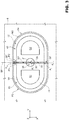
Figure 4 is a schematic top view of a further embodiment of the present sensing device, with portions removed; -
Figure 5 is a schematic illustration of a portion of a cross-section of a first semiconductor wafer, during a step of a manufacturing process; -
Figure 6 is a schematic illustration of a portion of a cross-section of a second semiconductor wafer, during a step of the manufacturing process; and -
Figures 7 and8 are schematic illustrations of a portion of a cross-section of a set of two semiconductor wafers, during two successive steps of the manufacturing process. -
Figure 2 shows anambient sensing device 50 of the semiconductor type, which, for reasons of brevity and without this implying any loss of generality, is now described with reference to the differences with respect to the sensing device 1 illustrated inFigure 1 . Elements already present in the sensing device 1 shown inFigure 1 are designated by the same references, except where otherwise specified. - In detail, and without this implying any loss of generality, the
ambient sensing device 50 comprises asecond bottom metallization 30, which is co-planar with thefirst bottom metallization 10, and is therefore arranged on the first surface S4, in contact with theepitaxial region 4, and is overlaid by thefirst passivation layer 6. Moreover, thesecond bottom metallization 30 is laterally staggered with respect to thefirst bottom metallization 10, in the direction of theactive area 15 so as to be arranged underneath thecavity 20. The first andsecond bottom metallizations - The
ambient sensing device 50 further comprises atop metallization structure 32, which in turn comprises a pair of metallizations, referred to in what follows as the first and second filtering metallizations M1, M2. - The first and second filtering metallizations M1, M2 are co-planar and are arranged laterally staggered over the part of
first passivation layer 6 that coats thesecond bottom metallization 30. - In detail, the first and second filtering metallizations M1, M2 have a same thickness (for example, equal to 1 µm), are made, for example, of aluminium, and are laterally staggered so as to delimit a
channel 35 having an elongated shape, which extends in a direction parallel to an axis X of an orthogonal reference system XYZ such that the plane XY is parallel to the first surface S4. - In greater detail, as shown in
Figure 3 , the first and second filtering metallizations M1, M2 have, for example, shapes symmetrical with respect to a plane of symmetry SP, parallel to the plane XZ. In addition, the first and second filtering metallizations M1, M2 are delimited, respectively, by a first and a second side wall P1, P2, which have the shape of rectangles parallel to the plane ZX and face one another. The first and second side walls P1, P2, laterally delimit thechannel 35; furthermore, thechannel 35 is delimited at the bottom by thefirst passivation layer 6. - Moreover, the first and second filtering metallizations M1, M2 are also laterally delimited by a third and a fourth side wall P3, P4, respectively, each of which has, for example, a curved shape with single concavity, with concavities opposite to one another. Without this implying any loss of generality, the first and second filtering metallizations M1, M2 have a shape of two half-shells arranged in front of one another, the envelope of which defines, approximately and in top view, a flattened ellipse along the minor axis. In addition, the first and second filtering metallizations M1, M2 are delimited at the top, respectively, by a first and a second top surface T1, T2, which are mutually co-planar and parallel to the plane XY.
- The
second passivation layer 8 coats a peripheral portion of the ensemble formed by the first and second filtering metallizations M1, M2 so as to delimit awindow 40, referred to in what follows as thefiltering window 40. - The
filtering window 40 has a closed shape, in top view, and faces the first and second top surfaces T1, T2; for example, thefiltering window 40 has an approximately elliptical shape. In particular, thesecond passivation layer 8 extends on peripheral portions of the first and second top surfaces T1, T2, and hence covers the third and fourth side walls P3, P4, whereas thefiltering window 40 faces central portions of the first and second top surfaces T1, T2. Thefiltering window 40 then leaves the first and second side walls P1, P2, and hence thechannel 35, exposed. - The
cap 18 further comprises a projectingregion 42, referred to in what follows as the projectingfiltering region 42. - The projecting
filtering region 42 extends downwards, starting from the third surface S18, in the direction of themain body 17. Moreover, the projectingfiltering region 42 is made of the same material (for example, a semiconductor) as theprimary body 19 of thecap 18, with which it forms a single piece. - In greater detail, as may be seen in
Figure 3 , in top view the projectingfiltering region 42 has, for example and to a first approximation, the shape of a flattened ellipse along the minor axis so as to form a profile including two parallel segments, the ends of which are connected by a pair of curved lines. - In addition, the projecting
filtering region 42 extends at the bottom until it partially penetrates into thefiltering window 40. In this connection, without this implying any loss of generality, the projectingfiltering region 42 has a cross-section with an area smaller than the area of thefiltering window 40 and extends within the latter, without contacting thesecond passivation layer 8, hence without contacting the edge of thefiltering window 40. Furthermore, the projectingfiltering region 42 is delimited, at the bottom, by a surface 44 (referred to in what follows as the coupling surface 44), which is parallel to the plane XY and overlies, in direct contact, the first and second top surfaces T1, T2 of the first and second filtering metallizations M1, M2. - The
hole 25 extends not only through theprimary body 19 of thecap 18 but also through the projectingfiltering region 42, until it gives out onto thecoupling surface 44. Purely by way of example, thehole 25 has an axis (designated by Z' inFigures 2 and3 ), which lies in the plane of symmetry SP. To a first approximation, the axis (not shown) of thechannel 35 is parallel to the axis X and lies in the plane of symmetry SP. - Without this implying any loss of generality, the projecting
filtering region 42 and thefiltering window 40 each have shapes symmetrical with respect to the plane of symmetry SP. Moreover, in the embodiment illustrated inFigure 3 , thechannel 35 is symmetrical with respect to the plane of symmetry SP; in particular, thechannel 35 has the shape of a parallelepiped. - The
ambient sensing device 50 further comprises a first and a second junction region G1, G2, which are made, for example, of an aluminium-germanium eutectic alloy and are approximately symmetrical with respect to the plane of symmetry SP. The first and second junction regions G1, G2 fix the projectingfiltering region 42 to thetop metallization structure 32. - In greater detail, the first junction region G1 is interposed, in direct contact, between the projecting
filtering region 42 and the first filtering metallization M1. In particular, a bottom portion of the first junction region G1 extends underneath the first top surface T1, and hence also underneath thecoupling surface 44, within the first filtering metallization M1, whereas a top portion of the first junction region G1 extends above the first top surface T1, and hence also above thecoupling surface 44, within the projectingfiltering region 42. - Likewise, the second junction region G2 is interposed, in direct contact, between the projecting
filtering region 42 and the second filtering metallization M2. In particular, a bottom portion of the second junction region G2 extends underneath the second top surface T2, and hence also underneath thecoupling surface 44, within the second filtering metallization M2, whereas a top portion of the second junction region G2 extends above the second top surface T2, and hence also above thecoupling surface 44, within the projectingfiltering region 42. - Without this implying any loss of generality, the first and second junction regions G1, G2 have planar shapes and are separate from one another. In top view, the first and second junction regions G1, G2 are arranged on opposite sides of the
channel 35, as well as at a distance from thechannel 35 and from thehole 25. - In greater detail, the diameter of the
hole 25, denoted by D, is, for example equal to 10 µm. Moreover, the width of thechannel 35, denoted by d, understood as the distance between the first and second side walls P1, P2, may be less than 10 µm and equal, for example, to 1 µm. In addition, thechannel 35 has a height, measured in a direction parallel to the axis Z, equal to the thickness of the first and second filtering metallizations M1, M2, and hence, as mentioned previously, for example equal to 1 µm. The first and second junction regions G1, G2 have a thickness (in a direction parallel to the axis Z) for example of 1 µm. - The
channel 35 hence has a cross-section (in planes parallel to the plane ZY), which is approximately rectangular and has an area smaller than the area of the cross-section (in planes parallel to the plane XY) of thehole 25. - Once again with reference to the
hole 35, a bottom portion thereof faces an underlying portion of thechannel 35, with which it is hence in fluidic communication. - In greater detail, as shown in
Figure 3 , thechannel 35 comprises acentral portion 36, through which the axis Z' passes; saidcentral portion 36 is overlaid by thehole 25. - Furthermore, the
channel 35 comprises a first and a secondintermediate portion 37', 37", which are arranged in a symmetrical way with respect to thecentral portion 36, to which they are adjacent. The first and secondintermediate portions 37', 37" are closed at the top by corresponding portions of the projectingfiltering region 42. - The
channel 35 further comprises a first and a secondperipheral portion 38', 38", which are adjacent, respectively, to the first and secondintermediate portions 37', 37". The first and secondperipheral portions 38', 38" are symmetrical with respect to the ensemble formed by thecentral portion 36 and the first and secondintermediate portions 37', 37". Moreover, in top view, the first and secondperipheral portions 38', 38" are arranged on the outside of the projectingfiltering region 42. - In greater detail, while the projecting
filtering region 42 occupies a central portion of thefiltering window 40, the first and secondperipheral portions 38', 38" of thechannel 35 face corresponding peripheral portions of the overlyingfiltering window 40, which communicate with thecavity 20. In turn, thecavity 20 is coupled to thehole 25 through the first and secondperipheral portions 38', 38" of thechannel 35, which define corresponding lateral openings of thechannel 35, which face upwards (designated, respectively, by Ae1 and Ae2 inFigure 3 ). Thechannel 35 is moreover centrally coupled to thehole 25 through a corresponding opening defined by the central portion 36 (designated by Ai), said opening Ai also facing upwards. - Purely by way of example, the first and second
peripheral portions 38', 38" of thechannel 35 have a length (measured in a direction parallel to the axis X) for example, of 10 µm. - Operatively, the first and second filtering metallizations M1, M2, the
filtering window 40, the first and second junction regions G1, G2 and the projectingfiltering region 42 form a filtering structure 99 (Figure 2 ), which sets thecavity 20 in fluidic communication with thehole 25, and hence enables a fluid present in the external world to penetrate into thecavity 20 so as to enable theactive area 15 to vary, for example, the value of at least one electrical parameter, as a function of a chemical or physical characteristic of the fluid, and thus enable measurement of this characteristic. In addition, on account of the small cross-section of thechannel 35, thefiltering structure 99 acts as a mechanical filter, which prevents entry into thecavity 20 of undesired particles, which, according to the application and the consequent sizing of thechannel 35, may include solid particles, fluid particles (for example, drops of water), etc. In particular, on account of the small cross-section, thechannel 35 performs a mechanical filtering that is finer than would be obtained by just thehole 25. - Once again with reference to the filtering capacity of the
filtering structure 99, this enables thehole 25 to have the dimensions that can be obtained using current manufacturing processes since the task of filtering is not performed by thehole 25. Furthermore, thefiltering structure 99 may be produced by means of so-called front-end manufacturing techniques, as described hereinafter. - Embodiments that include a number of channels are moreover possible, as shown for example in
Figure 4 , where anambient sensing device 100 is illustrated, which is now described as regards the differences with respect to theambient sensing device 50. For simplicity of representation,Figure 4 does not illustrate thesecond passivation layer 8. - In detail, the top metallization structure, here designated by 132 comprises eight filtering metallizations, designated, respectively, by M1'-M8', which are planar and mutually co-planar, have the same thickness, and are made of a same metal material (for example, aluminium).
- The filtering metallizations M1'-M8' are arranged angularly so that adjacent filtering metallizations delimit a corresponding channel; the channels are here designated by CH1-CH8.
- To a first approximation, in top view the filtering metallizations M1'-M8' have the shape of wedges of a region equal to the envelope of the filtering metallizations M1'-M8', each of these wedges being laterally delimited by corresponding pairs of rectangular plane side walls that depart from a corresponding vertex. In particular, the wedge of the i-th filtering metallization Mi' is delimited by a respective first side wall Pi1 and by a respective second side wall Pi2. The i-th channel CHi is laterally delimited by the first side wall and the second side wall, which delimit, respectively, a first and a second filtering metallization that are angularly adjacent to one another, said first and second side walls being parallel to one another.
- Without this implying any loss of generality, the axes (not illustrated) of the channels CH1-CH8 are angularly equispaced, with a spacing of 45°.
- In practice, the channels CH1-CH8 depart radially, in a symmetrical way with respect to the axis Z', starting from a
central volume 150, arranged underneath thehole 25, and on which the vertices of the wedge-like shapes of the filtering metallizations M1'-M8' face. - The projecting filtering region, here designated by 142, has, for example, a cylindrical shape, in which the
hole 25 extends, which overlies the aforementionedcentral volume 150. - With reference for brevity only to the first channel CH1 (but the same considerations apply to the other channels CH2-CH7), the
hole 25 overlies a corresponding central portion (designated by CH1'), which is adjacent to thecentral volume 150; the central portion CH1' hence communicates with thehole 25. In addition, the projectingfiltering region 142 closes, at the top, an intermediate portion CH1" of the first channel CH1, which is interposed between the central portion CH1' and a peripheral portion CH1''' of the first channel CH1. In top view, the peripheral portion CH1''' is arranged on the outside of the projectingfiltering region 142, within the filtering window, designated by 140 inFigure 4 (where for simplicity thefiltering window 140 is assumed to coincide, in top view, with the envelope of the filtering metallizations M1'-M8'). In practice, whereas the projectingfiltering region 142 occupies a central portion of thefiltering window 140, the peripheral portion CH1''' of the first channel CH1 faces a corresponding peripheral portion of the overlyingfiltering window 140, so as to communicate with the cavity 20 (not illustrated inFigure 4 ). Thecavity 20 is hence coupled to thehole 25 through the central portion CH1' and the peripheral portion CH1''' of the first channel CH1, which define corresponding lateral openings of the first channel CH1, facing upwards and designated, respectively, by Ai' and Ae'. - The
ambient sensing device 100 further comprises, for each filtering metallization M1'-M8', a corresponding junction region G1'-G8', which is made, for example, of a germanium-aluminium eutectic alloy and is interposed, in direct contact, between the corresponding filtering metallization M1'-M8' and the projectingfiltering region 142. Without this implying any loss of generality, to a first approximation the junction regions G1'-G8' are angularly equispaced and are arranged, in top view, outside of thehole 25. - In greater detail with reference, for simplicity, to just the first filtering metallization M1' and to the first junction region G1' (but the same considerations apply to the other filtering metallizations M2'-M8' and the other junction regions G2'-G8'), and referring to the first top surface T1' to indicate the surface that delimits the first filtering metallization M1' at the top, and referring to the coupling surface 144 to indicate the surface that delimits the projecting
filtering region 142 at the bottom, what is described hereinafter occurs. - The coupling surface 144 and the first top surface T1' are approximately co-planar since the projecting
filtering region 142 contacts the first filtering metallization M1'. Furthermore, albeit not shown, a bottom portion of the first junction region G1' extends underneath the first top surface T1', within the first filtering metallization M1', whereas a top portion of the first junction region G1' extends above the first top surface T1', within the projectingfiltering region 142, similarly to what is illustrated inFigure 2 . - The width of each of the channels CH1-CH8 (measured in a direction perpendicular to the radial direction) is, for example, equal to the aforementioned width d. Moreover, the channels CH1-CH8 perform the same function of mechanical filtering as that performed by the
channel 35 of the embodiment illustrated inFigures 2 and3 , affording the same advantages. - The embodiments described envisage fluidic coupling of the
cavity 20 to thehole 25, through one or more channels, each of which has at least a section, in a plane perpendicular to its own direction of extension, that has an area smaller than the area of the section of thehole 25 that has the minimum area from among the sections of thehole 25 in planes perpendicular to the direction of extension of thehole 25. In addition, or as an alternative, it is possible for the function of fine filtering to be performed by at least one of the aforementioned upward-facing openings of the channel, in which case said opening/s has/have an area smaller than the area of the section of thehole 25 that has the minimum area from among the sections of thehole 25 in planes perpendicular to the direction of extension of thehole 25. - Advantageously, the present ambient sensing device can be manufactured by implementing the following manufacturing process, which is described with reference, by way of example, to manufacturing of the ambient sensing device illustrated in
Figures 2 and3 . - As shown in
Figure 5 , initially afirst semiconductor wafer 200 is provided, which is machined so as to form themain body 17. As a result, thefirst wafer 200 comprises thesemiconductor body 2, the first andsecond bottom metallizations top metallization 12, thetop metallization structure 32, the first and thesecond passivation layer first wafer 200 comprises the sealingwindow 14 and thefiltering window 40. - Furthermore, the
first wafer 200 comprises thechannel 35, which is, in fact, formed using so-called front-end techniques, by means of appropriate spacing of the first and second filtering metallizations M1, M2. - Moreover, as shown in
Figure 6 , asecond semiconductor wafer 202 is provided, which forms thecap 18. In particular, thesecond wafer 202 is machined so as to form theprimary body 19, the projectingregion 22, the projectingfiltering region 42 and thehole 25. - The projecting
filtering region 42 is delimited, at the top, by thecoupling surface 44, on which a first and a second preliminary region G1*, G2* extend, which are made, for example, of germanium and are designed to form, respectively, the first and second junction regions G1, G2. Moreover, the projectingregion 22 is delimited, at the top, by a temporary surface Spb, on which a thirdpreliminary region 23* extends, which is made, for example, of germanium and is designed to form thejunction region 23. The first, second and third preliminary regions G1*, G2*, 23* have a thickness of, for example, 0.5 µm. - Next, as shown in
Figure 7 , thesecond wafer 202 is flipped over and is coupled to thefirst wafer 200 so that the first and second preliminary regions G1*, G2* contact, respectively, the first and second top surfaces T1, T2 of the first and second filtering metallizations M1, M2, within thefiltering window 40, and moreover so that the thirdpreliminary region 23* contacts the exposed part of the firsttop metallization 12, within the sealingwindow 14. - In addition, a bonding process is carried out at a temperature higher than the melting point of the eutectic alloy that forms the
junction region 23 and the first and second junction regions G1, G2. In this way, there occurs interaction between germanium and aluminium and consequent transformation of the first, second and third preliminary regions G1*, G2*, 23*, respectively, into the first and second junction regions G1, G2 and into thejunction region 23. Furthermore, the portions of thecoupling surface 44 left exposed by the first and second preliminary regions G1*, G2*, previously (Figure 7 ) separated by the first and second top surfaces T1, T2 of the first and second filtering metallizations M1, M2 abut upon the latter. There is thus formed, as shown inFigure 8 , a device that is the same as theambient sensing device 50 illustrated inFigure 2 , but without thehole 25, which is formed subsequent to bonding, using common machining techniques of a deep-silicon-etching type (step not shown) so as to obtain theambient sensing device 50 illustrated inFigure 2 . In a per se known manner, dicing/singulation operations can then be carried out. - Finally, it is clear that modifications and variations may be made to what has been described and illustrated herein, without departing from the scope of the present invention, as defined in the annexed claims.
- For instance, as mentioned previously, the first and/or the
second bottom metallization - The exact alignment of the
filtering window 40, in particular with reference to the side walls P1-P4 of the first and second filtering metallizations M1, M2, may vary with respect to what has been described. - The coupling between the
projection 22 of thecap 18 and the firsttop metallization 12, and hence the lateral sealing of thecavity 20, may be obtained in a way different from what has been described. Likewise, thejunction region 23 may have a shape and arrangement different from the one described. - In general, materials may be used different from the materials described previously. For instance, coupling between the projecting filtering region and the top metallization structure may be obtained in a way different from what has been described. In particular, the preliminary regions and the top metallization structure may be made of materials such as to enable formation of a metal bonding other than aluminium-germanium, such as for example a gold-gold or gold-tin bonding. Furthermore, bonding may be not only of a fusion type but also of an anodic type, or of a type selected from among: glass-frit, polymeric or dry-film, etc. In this case, the metallization structure is replaced by a coupling structure, which has, for example, the same shape as the metallization structure described previously, but is made of a material that may be different from a metal material, such as a dielectric or semiconductor material. The coupling structure is bonded to the projecting filtering region of the cap.
- In addition, the cap may not only be made of any semiconductor (for example, silicon carbide) but also of any substrate currently used in the manufacture of integrated circuits, such as for example a vitreous substrate.
- Finally, as mentioned previously, the hole in the cap may have, along the axis Z', a section of variable shape, in which case, with reference, for brevity, to a single channel, the section and/or the opening or openings have/has an area smaller than the area of the section of the hole that has the minimum area from among the sections of the hole in planes perpendicular to the direction of extension of the hole.
Claims (18)
- A semiconductor device for ambient sensing comprising:- a cap (18) traversed by a hole (25); and- a main body (17) mechanically coupled to the cap (18) so as to delimit a cavity (20), which is interposed between the main body and the cap;and wherein the main body comprises a semiconductor body (2) and a coupling structure (32; 132), which is interposed between the semiconductor body and the cap and laterally delimits a channel (35; CH1-CH8) that fluidically couples the cavity and the hole, said channel being configured to perform a mechanical filtering that is finer than the mechanical filtering performed by the hole.
- The semiconductor device according to claim 1, wherein the channel (35; CH1-CH8) has at least a cross-section with area smaller than the area of the cross-section of the hole (25) that has the minimum area.
- The semiconductor device according to claim 1 or 2, wherein the channel (35; CH1-CH8) delimits a first and a second opening (Ai, Ae1; Ai', Ae'), which are laterally staggered and face, respectively, onto the hole (25) and onto a part of the cavity (20); and wherein at least one of the first and the second openings has an area smaller than the area of the cross-section of the hole having the minimum area.
- The semiconductor device according to any one of the preceding claims, wherein the channel (35; CH1-CH8) extends in a direction transverse to the hole (25).
- The semiconductor device according to any one of the preceding claims, wherein the semiconductor body (2) is delimited by a front surface (S4); and wherein the channel (35; CH1-CH8) extends in a direction parallel to the front surface.
- The semiconductor device according to any one of the preceding claims, wherein the main body (17) further comprises a dielectric region (6, 8), which overlies the semiconductor body (2); and wherein the channel (35; CH1-CH8) is delimited at the bottom by the dielectric region.
- The semiconductor device according to any one of the preceding claims, wherein the cap (18) comprises a primary body (19), which overlies the main body (17) at a distance, and a projecting region (42; 142), which extends starting from the primary body in the direction of the main body; and wherein the hole (25) traverses the primary body and the projecting region; and wherein the projecting region is bonded to the coupling structure (32; 132) so as to close a part of the channel (35; CH1-CH8) facing the cap.
- The semiconductor device according to claim 7, wherein the channel (35; CH1-CH8) comprises at least:- a central portion (36; CH1'), which is arranged underneath the hole (25) and is open towards the cap (18) so as to communicate with the hole;- an intermediate portion (37'; CH1"), which is laterally staggered with respect to the hole and is overlaid by the projecting region (42; 142); and- a peripheral portion (38', CH1"'), which is laterally staggered with respect to the projecting region and is open towards the cap so as to communicate with the cavity (20), the intermediate portion being interposed between the central portion and the peripheral portion.
- The semiconductor device according to claim 7 or 8, further comprising at least one junction region (G1, G2; G1'-G8'), which is formed by a eutectic alloy and is interposed, in direct contact, between the projecting region (42; 142) and the coupling structure (32; 132), said junction region being laterally staggered with respect to the channel (35; CH1-CH8).
- The semiconductor device according to claim 9, wherein part of the projecting region (42; 142) contacts the coupling structure (32; 132); and wherein the junction region (G1, G2; G1'-G8') extends in part in the projecting region and in part in the coupling structure.
- The semiconductor device according to any one of the preceding claims, wherein the coupling structure (32; 132) comprises a plurality of co-planar coupling regions (M1, M2; M1'-M8'); and wherein the channel (35; CH1-CH8) is laterally delimited by a pair of said coupling regions.
- The semiconductor device according to any one of the preceding claims, wherein the coupling structure (32; 132) is made of metal material.
- The semiconductor device according to any one of the preceding claims, wherein the cap (18) is made of semiconductor or vitreous material.
- A process for manufacturing a semiconductor device (50; 100) for ambient sensing, comprising the steps of:- forming a main body (17) including a semiconductor body (2) and a coupling structure (32; 132) that laterally delimits a channel (35; CH1-CH8);- forming a cap (18) traversed by a hole (25); and- mechanically coupling the main body to the cap so as to delimit a cavity (20), which is interposed between the main body and the cap, and so that the coupling structure will be interposed between the semiconductor body and the cap, and said channel will fluidically couple the cavity and the hole and will be configured to perform a mechanical filtering that is finer than the mechanical filtering performed by the hole.
- The manufacturing process according to claim 14, wherein the step of forming a main body (17) is carried out starting from a first wafer (200); and wherein the step of forming a cap (18) comprises:- starting from a second wafer (202), forming a primary body (19) and a projecting region (42; 142), which extends starting from the primary body; and- forming the hole (25) so that it will traverse the primary body and the projecting region;and wherein said step of mechanically coupling the main body to the cap comprises carrying out a step of bonding the first and second wafers, which comprises bonding the projecting region (42; 142) to the coupling structure (32; 132); and wherein said step of forming the hole is carried out after the step of bonding the first and second wafers.
- The manufacturing process according to claim 15, further comprising the step of closing, by means of the projecting region (42; 142), a part of the channel (35; CH1-CH8) facing the cap.
- The manufacturing process according to claim 15 or claim 16, wherein the step of bonding the projecting region (42; 142) to the coupling structure (32; 132) comprises forming at least one junction region (G1, G2; G1'-G8') made of a eutectic alloy, interposed between the projecting region and the coupling structure.
- The manufacturing process according to claim 17, wherein the coupling structure (32; 132) is made of a first material, said process further comprising the step of:- before carrying out bonding of the first and second wafers (200, 202), forming on the projecting region (42) at least one preliminary region (G1*, G2*) of a second material, laterally staggered with respect to the hole (25);and wherein said step of carrying out bonding of the first and second wafers is carried out so as to form the junction region (G1, G2; G1'-G8') following upon formation of said eutectic alloy between the first material of the coupling structure and the second material of the preliminary region.
Applications Claiming Priority (1)
| Application Number | Priority Date | Filing Date | Title |
|---|---|---|---|
| IT102020000003862A IT202000003862A1 (en) | 2020-02-25 | 2020-02-25 | SEMICONDUCTOR DEVICE FOR ENVIRONMENTAL DETECTION INCLUDING A CAVITY THAT CAN BE COUPLED TO THE EXTERNAL WORLD AND A MECHANICAL FILTRATION STRUCTURE AND CORRESPONDING MANUFACTURING PROCESS |
Publications (2)
| Publication Number | Publication Date |
|---|---|
| EP3872472A1 true EP3872472A1 (en) | 2021-09-01 |
| EP3872472B1 EP3872472B1 (en) | 2022-10-05 |
Family
ID=70480768
Family Applications (1)
| Application Number | Title | Priority Date | Filing Date |
|---|---|---|---|
| EP21159179.7A Active EP3872472B1 (en) | 2020-02-25 | 2021-02-25 | Semiconductor device for ambient sensing including a cavity and corresponding manufacturing process. |
Country Status (4)
| Country | Link |
|---|---|
| US (2) | US11513016B2 (en) |
| EP (1) | EP3872472B1 (en) |
| CN (2) | CN215952845U (en) |
| IT (1) | IT202000003862A1 (en) |
Families Citing this family (1)
| Publication number | Priority date | Publication date | Assignee | Title |
|---|---|---|---|---|
| IT202000003862A1 (en) | 2020-02-25 | 2021-08-25 | St Microelectronics Srl | SEMICONDUCTOR DEVICE FOR ENVIRONMENTAL DETECTION INCLUDING A CAVITY THAT CAN BE COUPLED TO THE EXTERNAL WORLD AND A MECHANICAL FILTRATION STRUCTURE AND CORRESPONDING MANUFACTURING PROCESS |
Citations (2)
| Publication number | Priority date | Publication date | Assignee | Title |
|---|---|---|---|---|
| US20030167852A1 (en) | 2002-03-11 | 2003-09-11 | Mks Instruments, Inc. | Surface area deposition trap |
| US20060169049A1 (en) | 2005-01-31 | 2006-08-03 | Sanyo Electric Co., Ltd. | Semiconductor sensor |
Family Cites Families (8)
| Publication number | Priority date | Publication date | Assignee | Title |
|---|---|---|---|---|
| US5062302A (en) | 1988-04-29 | 1991-11-05 | Schlumberger Industries, Inc. | Laminated semiconductor sensor with overpressure protection |
| SG111092A1 (en) | 2002-11-15 | 2005-05-30 | St Microelectronics Pte Ltd | Semiconductor device package and method of manufacture |
| US7526962B1 (en) | 2008-01-18 | 2009-05-05 | Kulike Semiconductor Products, Inc. | High pressure delta P sensor |
| US9010190B2 (en) | 2012-04-20 | 2015-04-21 | Rosemount Aerospace Inc. | Stress isolated MEMS structures and methods of manufacture |
| EP2806258B1 (en) | 2013-05-20 | 2018-09-12 | ams international AG | Differential pressure sensor |
| TWI550261B (en) | 2014-03-17 | 2016-09-21 | 立錡科技股份有限公司 | Mirco-electro-mechanical system pressure sensor and manufacturing method thereof |
| ITUA20164673A1 (en) | 2016-06-27 | 2017-12-27 | St Microelectronics Srl | MEMS DEVICE FORMED BY AT LEAST TWO MULTI-PURPOSED STRUCTURAL LAYERS AND RELATIVE PROCESS OF MANUFACTURE |
| IT202000003862A1 (en) * | 2020-02-25 | 2021-08-25 | St Microelectronics Srl | SEMICONDUCTOR DEVICE FOR ENVIRONMENTAL DETECTION INCLUDING A CAVITY THAT CAN BE COUPLED TO THE EXTERNAL WORLD AND A MECHANICAL FILTRATION STRUCTURE AND CORRESPONDING MANUFACTURING PROCESS |
-
2020
- 2020-02-25 IT IT102020000003862A patent/IT202000003862A1/en unknown
-
2021
- 2021-02-04 US US17/168,059 patent/US11513016B2/en active Active
- 2021-02-24 CN CN202120411262.2U patent/CN215952845U/en not_active Withdrawn - After Issue
- 2021-02-24 CN CN202110209989.7A patent/CN113375854B/en active Active
- 2021-02-25 EP EP21159179.7A patent/EP3872472B1/en active Active
-
2022
- 2022-10-03 US US17/958,761 patent/US11802805B2/en active Active
Patent Citations (2)
| Publication number | Priority date | Publication date | Assignee | Title |
|---|---|---|---|---|
| US20030167852A1 (en) | 2002-03-11 | 2003-09-11 | Mks Instruments, Inc. | Surface area deposition trap |
| US20060169049A1 (en) | 2005-01-31 | 2006-08-03 | Sanyo Electric Co., Ltd. | Semiconductor sensor |
Also Published As
| Publication number | Publication date |
|---|---|
| US20230029120A1 (en) | 2023-01-26 |
| EP3872472B1 (en) | 2022-10-05 |
| US20210262884A1 (en) | 2021-08-26 |
| CN113375854B (en) | 2024-06-11 |
| US11802805B2 (en) | 2023-10-31 |
| CN113375854A (en) | 2021-09-10 |
| IT202000003862A1 (en) | 2021-08-25 |
| US11513016B2 (en) | 2022-11-29 |
| CN215952845U (en) | 2022-03-04 |
Similar Documents
| Publication | Publication Date | Title |
|---|---|---|
| US6159761A (en) | Method of manufacturing a force sensor having an electrode which changes resistance or electrostatic capacitance in response to force | |
| CN111704104B (en) | Method for producing a MEMS pressure sensor and corresponding MEMS pressure sensor | |
| US20190120710A1 (en) | Pressure sensor generating a transduced signal with reduced ambient temperature dependence, and manufacturing method thereof | |
| CN105424090B (en) | MEMS piezoresistive composite sensor and processing method thereof | |
| JP5206726B2 (en) | Mechanical quantity detection device and manufacturing method thereof | |
| US20170343438A1 (en) | Differential pressure sensor full overpressure protection device | |
| CN105353167A (en) | MEMS piezoresistive type acceleration sensor and processing method for the same | |
| JPH09199496A (en) | Micromechanical device and manufacturing method thereof | |
| EP3872472B1 (en) | Semiconductor device for ambient sensing including a cavity and corresponding manufacturing process. | |
| US11840445B2 (en) | MEMS sensor including a diaphragm and method for manufacturing a MEMS sensor | |
| EP2873958B1 (en) | Capacitive pressure sensors for high temperature applications | |
| KR20010074906A (en) | Micromechanical component and its production method | |
| US5946549A (en) | Method for manufacturing sensor using semiconductor | |
| US6755084B2 (en) | Pressure sensor and method of manufacturing pressure sensor | |
| US7243546B2 (en) | Acceleration sensor chip | |
| EP3557212B1 (en) | High temperature capacitive mems pressure sensor | |
| JPH03114272A (en) | Strain sensor and manufacture thereof | |
| CN119984579A (en) | Micro-electro-mechanical pressure sensor and method for manufacturing a micro-electro-mechanical pressure sensor | |
| US20260118197A1 (en) | Pressure sensor having high detection performance and optimized manufacturing | |
| US20210206627A1 (en) | Semiconductor structure and manufacturing method for the same | |
| US11879800B2 (en) | MEMS strain gauge pressure sensor with mechanical symmetries | |
| CN121933183A (en) | Pressure sensor with high detection performance and optimized manufacture | |
| US20250276893A1 (en) | Microelectromechanical sensor with improved external fluidic coupling and manufacturing process thereof | |
| CN120553629A (en) | Microelectromechanical sensor with improved external fluid coupling and manufacturing process thereof | |
| JP4570993B2 (en) | Acceleration sensor and manufacturing method thereof |
Legal Events
| Date | Code | Title | Description |
|---|---|---|---|
| PUAI | Public reference made under article 153(3) epc to a published international application that has entered the european phase |
Free format text: ORIGINAL CODE: 0009012 |
|
| STAA | Information on the status of an ep patent application or granted ep patent |
Free format text: STATUS: THE APPLICATION HAS BEEN PUBLISHED |
|
| AK | Designated contracting states |
Kind code of ref document: A1 Designated state(s): AL AT BE BG CH CY CZ DE DK EE ES FI FR GB GR HR HU IE IS IT LI LT LU LV MC MK MT NL NO PL PT RO RS SE SI SK SM TR |
|
| STAA | Information on the status of an ep patent application or granted ep patent |
Free format text: STATUS: REQUEST FOR EXAMINATION WAS MADE |
|
| 17P | Request for examination filed |
Effective date: 20220228 |
|
| RBV | Designated contracting states (corrected) |
Designated state(s): AL AT BE BG CH CY CZ DE DK EE ES FI FR GB GR HR HU IE IS IT LI LT LU LV MC MK MT NL NO PL PT RO RS SE SI SK SM TR |
|
| INTG | Intention to grant announced |
Effective date: 20220422 |
|
| INTG | Intention to grant announced |
Effective date: 20220429 |
|
| GRAS | Grant fee paid |
Free format text: ORIGINAL CODE: EPIDOSNIGR3 |
|
| STAA | Information on the status of an ep patent application or granted ep patent |
Free format text: STATUS: GRANT OF PATENT IS INTENDED |
|
| GRAA | (expected) grant |
Free format text: ORIGINAL CODE: 0009210 |
|
| STAA | Information on the status of an ep patent application or granted ep patent |
Free format text: STATUS: THE PATENT HAS BEEN GRANTED |
|
| AK | Designated contracting states |
Kind code of ref document: B1 Designated state(s): AL AT BE BG CH CY CZ DE DK EE ES FI FR GB GR HR HU IE IS IT LI LT LU LV MC MK MT NL NO PL PT RO RS SE SI SK SM TR |
|
| REG | Reference to a national code |
Ref country code: GB Ref legal event code: FG4D |
|
| REG | Reference to a national code |
Ref country code: CH Ref legal event code: EP |
|
| REG | Reference to a national code |
Ref country code: AT Ref legal event code: REF Ref document number: 1523007 Country of ref document: AT Kind code of ref document: T Effective date: 20221015 |
|
| REG | Reference to a national code |
Ref country code: IE Ref legal event code: FG4D |
|
| REG | Reference to a national code |
Ref country code: DE Ref legal event code: R096 Ref document number: 602021000496 Country of ref document: DE |
|
| REG | Reference to a national code |
Ref country code: LT Ref legal event code: MG9D |
|
| REG | Reference to a national code |
Ref country code: NL Ref legal event code: MP Effective date: 20221005 |
|
| REG | Reference to a national code |
Ref country code: AT Ref legal event code: MK05 Ref document number: 1523007 Country of ref document: AT Kind code of ref document: T Effective date: 20221005 |
|
| PG25 | Lapsed in a contracting state [announced via postgrant information from national office to epo] |
Ref country code: NL Free format text: LAPSE BECAUSE OF FAILURE TO SUBMIT A TRANSLATION OF THE DESCRIPTION OR TO PAY THE FEE WITHIN THE PRESCRIBED TIME-LIMIT Effective date: 20221005 |
|
| PG25 | Lapsed in a contracting state [announced via postgrant information from national office to epo] |
Ref country code: SE Free format text: LAPSE BECAUSE OF FAILURE TO SUBMIT A TRANSLATION OF THE DESCRIPTION OR TO PAY THE FEE WITHIN THE PRESCRIBED TIME-LIMIT Effective date: 20221005 Ref country code: PT Free format text: LAPSE BECAUSE OF FAILURE TO SUBMIT A TRANSLATION OF THE DESCRIPTION OR TO PAY THE FEE WITHIN THE PRESCRIBED TIME-LIMIT Effective date: 20230206 Ref country code: NO Free format text: LAPSE BECAUSE OF FAILURE TO SUBMIT A TRANSLATION OF THE DESCRIPTION OR TO PAY THE FEE WITHIN THE PRESCRIBED TIME-LIMIT Effective date: 20230105 Ref country code: LT Free format text: LAPSE BECAUSE OF FAILURE TO SUBMIT A TRANSLATION OF THE DESCRIPTION OR TO PAY THE FEE WITHIN THE PRESCRIBED TIME-LIMIT Effective date: 20221005 Ref country code: FI Free format text: LAPSE BECAUSE OF FAILURE TO SUBMIT A TRANSLATION OF THE DESCRIPTION OR TO PAY THE FEE WITHIN THE PRESCRIBED TIME-LIMIT Effective date: 20221005 Ref country code: ES Free format text: LAPSE BECAUSE OF FAILURE TO SUBMIT A TRANSLATION OF THE DESCRIPTION OR TO PAY THE FEE WITHIN THE PRESCRIBED TIME-LIMIT Effective date: 20221005 Ref country code: AT Free format text: LAPSE BECAUSE OF FAILURE TO SUBMIT A TRANSLATION OF THE DESCRIPTION OR TO PAY THE FEE WITHIN THE PRESCRIBED TIME-LIMIT Effective date: 20221005 |
|
| PG25 | Lapsed in a contracting state [announced via postgrant information from national office to epo] |
Ref country code: RS Free format text: LAPSE BECAUSE OF FAILURE TO SUBMIT A TRANSLATION OF THE DESCRIPTION OR TO PAY THE FEE WITHIN THE PRESCRIBED TIME-LIMIT Effective date: 20221005 Ref country code: PL Free format text: LAPSE BECAUSE OF FAILURE TO SUBMIT A TRANSLATION OF THE DESCRIPTION OR TO PAY THE FEE WITHIN THE PRESCRIBED TIME-LIMIT Effective date: 20221005 Ref country code: LV Free format text: LAPSE BECAUSE OF FAILURE TO SUBMIT A TRANSLATION OF THE DESCRIPTION OR TO PAY THE FEE WITHIN THE PRESCRIBED TIME-LIMIT Effective date: 20221005 Ref country code: IS Free format text: LAPSE BECAUSE OF FAILURE TO SUBMIT A TRANSLATION OF THE DESCRIPTION OR TO PAY THE FEE WITHIN THE PRESCRIBED TIME-LIMIT Effective date: 20230205 Ref country code: HR Free format text: LAPSE BECAUSE OF FAILURE TO SUBMIT A TRANSLATION OF THE DESCRIPTION OR TO PAY THE FEE WITHIN THE PRESCRIBED TIME-LIMIT Effective date: 20221005 Ref country code: GR Free format text: LAPSE BECAUSE OF FAILURE TO SUBMIT A TRANSLATION OF THE DESCRIPTION OR TO PAY THE FEE WITHIN THE PRESCRIBED TIME-LIMIT Effective date: 20230106 |
|
| REG | Reference to a national code |
Ref country code: DE Ref legal event code: R097 Ref document number: 602021000496 Country of ref document: DE |
|
| PG25 | Lapsed in a contracting state [announced via postgrant information from national office to epo] |
Ref country code: SM Free format text: LAPSE BECAUSE OF FAILURE TO SUBMIT A TRANSLATION OF THE DESCRIPTION OR TO PAY THE FEE WITHIN THE PRESCRIBED TIME-LIMIT Effective date: 20221005 Ref country code: RO Free format text: LAPSE BECAUSE OF FAILURE TO SUBMIT A TRANSLATION OF THE DESCRIPTION OR TO PAY THE FEE WITHIN THE PRESCRIBED TIME-LIMIT Effective date: 20221005 Ref country code: EE Free format text: LAPSE BECAUSE OF FAILURE TO SUBMIT A TRANSLATION OF THE DESCRIPTION OR TO PAY THE FEE WITHIN THE PRESCRIBED TIME-LIMIT Effective date: 20221005 Ref country code: DK Free format text: LAPSE BECAUSE OF FAILURE TO SUBMIT A TRANSLATION OF THE DESCRIPTION OR TO PAY THE FEE WITHIN THE PRESCRIBED TIME-LIMIT Effective date: 20221005 Ref country code: CZ Free format text: LAPSE BECAUSE OF FAILURE TO SUBMIT A TRANSLATION OF THE DESCRIPTION OR TO PAY THE FEE WITHIN THE PRESCRIBED TIME-LIMIT Effective date: 20221005 |
|
| PLBE | No opposition filed within time limit |
Free format text: ORIGINAL CODE: 0009261 |
|
| STAA | Information on the status of an ep patent application or granted ep patent |
Free format text: STATUS: NO OPPOSITION FILED WITHIN TIME LIMIT |
|
| PG25 | Lapsed in a contracting state [announced via postgrant information from national office to epo] |
Ref country code: SK Free format text: LAPSE BECAUSE OF FAILURE TO SUBMIT A TRANSLATION OF THE DESCRIPTION OR TO PAY THE FEE WITHIN THE PRESCRIBED TIME-LIMIT Effective date: 20221005 Ref country code: AL Free format text: LAPSE BECAUSE OF FAILURE TO SUBMIT A TRANSLATION OF THE DESCRIPTION OR TO PAY THE FEE WITHIN THE PRESCRIBED TIME-LIMIT Effective date: 20221005 |
|
| 26N | No opposition filed |
Effective date: 20230706 |
|
| PG25 | Lapsed in a contracting state [announced via postgrant information from national office to epo] |
Ref country code: MC Free format text: LAPSE BECAUSE OF FAILURE TO SUBMIT A TRANSLATION OF THE DESCRIPTION OR TO PAY THE FEE WITHIN THE PRESCRIBED TIME-LIMIT Effective date: 20221005 |
|
| REG | Reference to a national code |
Ref country code: BE Ref legal event code: MM Effective date: 20230228 |
|
| PG25 | Lapsed in a contracting state [announced via postgrant information from national office to epo] |
Ref country code: LU Free format text: LAPSE BECAUSE OF NON-PAYMENT OF DUE FEES Effective date: 20230225 |
|
| PG25 | Lapsed in a contracting state [announced via postgrant information from national office to epo] |
Ref country code: SI Free format text: LAPSE BECAUSE OF FAILURE TO SUBMIT A TRANSLATION OF THE DESCRIPTION OR TO PAY THE FEE WITHIN THE PRESCRIBED TIME-LIMIT Effective date: 20221005 |
|
| REG | Reference to a national code |
Ref country code: IE Ref legal event code: MM4A |
|
| PG25 | Lapsed in a contracting state [announced via postgrant information from national office to epo] |
Ref country code: IE Free format text: LAPSE BECAUSE OF NON-PAYMENT OF DUE FEES Effective date: 20230225 Ref country code: FR Free format text: LAPSE BECAUSE OF NON-PAYMENT OF DUE FEES Effective date: 20230228 |
|
| PG25 | Lapsed in a contracting state [announced via postgrant information from national office to epo] |
Ref country code: BE Free format text: LAPSE BECAUSE OF NON-PAYMENT OF DUE FEES Effective date: 20230228 |
|
| PG25 | Lapsed in a contracting state [announced via postgrant information from national office to epo] |
Ref country code: IT Free format text: LAPSE BECAUSE OF FAILURE TO SUBMIT A TRANSLATION OF THE DESCRIPTION OR TO PAY THE FEE WITHIN THE PRESCRIBED TIME-LIMIT Effective date: 20221005 |
|
| REG | Reference to a national code |
Ref country code: CH Ref legal event code: PL |
|
| PG25 | Lapsed in a contracting state [announced via postgrant information from national office to epo] |
Ref country code: CH Free format text: LAPSE BECAUSE OF NON-PAYMENT OF DUE FEES Effective date: 20240229 |
|
| PG25 | Lapsed in a contracting state [announced via postgrant information from national office to epo] |
Ref country code: CH Free format text: LAPSE BECAUSE OF NON-PAYMENT OF DUE FEES Effective date: 20240229 |
|
| PG25 | Lapsed in a contracting state [announced via postgrant information from national office to epo] |
Ref country code: BG Free format text: LAPSE BECAUSE OF FAILURE TO SUBMIT A TRANSLATION OF THE DESCRIPTION OR TO PAY THE FEE WITHIN THE PRESCRIBED TIME-LIMIT Effective date: 20221005 |
|
| PG25 | Lapsed in a contracting state [announced via postgrant information from national office to epo] |
Ref country code: BG Free format text: LAPSE BECAUSE OF FAILURE TO SUBMIT A TRANSLATION OF THE DESCRIPTION OR TO PAY THE FEE WITHIN THE PRESCRIBED TIME-LIMIT Effective date: 20221005 |
|
| PG25 | Lapsed in a contracting state [announced via postgrant information from national office to epo] |
Ref country code: CY Free format text: LAPSE BECAUSE OF FAILURE TO SUBMIT A TRANSLATION OF THE DESCRIPTION OR TO PAY THE FEE WITHIN THE PRESCRIBED TIME-LIMIT; INVALID AB INITIO Effective date: 20210225 |
|
| PG25 | Lapsed in a contracting state [announced via postgrant information from national office to epo] |
Ref country code: HU Free format text: LAPSE BECAUSE OF FAILURE TO SUBMIT A TRANSLATION OF THE DESCRIPTION OR TO PAY THE FEE WITHIN THE PRESCRIBED TIME-LIMIT; INVALID AB INITIO Effective date: 20210225 |
|
| GBPC | Gb: european patent ceased through non-payment of renewal fee |
Effective date: 20250225 |
|
| PG25 | Lapsed in a contracting state [announced via postgrant information from national office to epo] |
Ref country code: TR Free format text: LAPSE BECAUSE OF FAILURE TO SUBMIT A TRANSLATION OF THE DESCRIPTION OR TO PAY THE FEE WITHIN THE PRESCRIBED TIME-LIMIT Effective date: 20221005 |
|
| PG25 | Lapsed in a contracting state [announced via postgrant information from national office to epo] |
Ref country code: GB Free format text: LAPSE BECAUSE OF NON-PAYMENT OF DUE FEES Effective date: 20250225 |
|
| PGFP | Annual fee paid to national office [announced via postgrant information from national office to epo] |
Ref country code: DE Payment date: 20260121 Year of fee payment: 6 |