EP3871250B1 - Packaging process for side-wall plating with a conductive film - Google Patents
Packaging process for side-wall plating with a conductive film Download PDFInfo
- Publication number
- EP3871250B1 EP3871250B1 EP20848928.6A EP20848928A EP3871250B1 EP 3871250 B1 EP3871250 B1 EP 3871250B1 EP 20848928 A EP20848928 A EP 20848928A EP 3871250 B1 EP3871250 B1 EP 3871250B1
- Authority
- EP
- European Patent Office
- Prior art keywords
- lead
- leads
- plating
- conductive film
- package assembly
- Prior art date
- Legal status (The legal status is an assumption and is not a legal conclusion. Google has not performed a legal analysis and makes no representation as to the accuracy of the status listed.)
- Active
Links
Images




Classifications
-
- H—ELECTRICITY
- H10—SEMICONDUCTOR DEVICES; ELECTRIC SOLID-STATE DEVICES NOT OTHERWISE PROVIDED FOR
- H10W—GENERIC PACKAGES, INTERCONNECTIONS, CONNECTORS OR OTHER CONSTRUCTIONAL DETAILS OF DEVICES COVERED BY CLASS H10
- H10W70/00—Package substrates; Interposers; Redistribution layers [RDL]
- H10W70/01—Manufacture or treatment
- H10W70/04—Manufacture or treatment of leadframes
- H10W70/048—Mechanical treatments, e.g. punching, cutting, deforming or cold welding
-
- H—ELECTRICITY
- H10—SEMICONDUCTOR DEVICES; ELECTRIC SOLID-STATE DEVICES NOT OTHERWISE PROVIDED FOR
- H10P—GENERIC PROCESSES OR APPARATUS FOR THE MANUFACTURE OR TREATMENT OF DEVICES COVERED BY CLASS H10
- H10P54/00—Cutting or separating of wafers, substrates or parts of devices
-
- H—ELECTRICITY
- H10—SEMICONDUCTOR DEVICES; ELECTRIC SOLID-STATE DEVICES NOT OTHERWISE PROVIDED FOR
- H10P—GENERIC PROCESSES OR APPARATUS FOR THE MANUFACTURE OR TREATMENT OF DEVICES COVERED BY CLASS H10
- H10P72/00—Handling or holding of wafers, substrates or devices during manufacture or treatment thereof
- H10P72/70—Handling or holding of wafers, substrates or devices during manufacture or treatment thereof for supporting or gripping
- H10P72/74—Handling or holding of wafers, substrates or devices during manufacture or treatment thereof for supporting or gripping using temporarily an auxiliary support
-
- H—ELECTRICITY
- H10—SEMICONDUCTOR DEVICES; ELECTRIC SOLID-STATE DEVICES NOT OTHERWISE PROVIDED FOR
- H10W—GENERIC PACKAGES, INTERCONNECTIONS, CONNECTORS OR OTHER CONSTRUCTIONAL DETAILS OF DEVICES COVERED BY CLASS H10
- H10W46/00—Marks applied to devices, e.g. for alignment or identification
-
- H—ELECTRICITY
- H10—SEMICONDUCTOR DEVICES; ELECTRIC SOLID-STATE DEVICES NOT OTHERWISE PROVIDED FOR
- H10W—GENERIC PACKAGES, INTERCONNECTIONS, CONNECTORS OR OTHER CONSTRUCTIONAL DETAILS OF DEVICES COVERED BY CLASS H10
- H10W70/00—Package substrates; Interposers; Redistribution layers [RDL]
- H10W70/01—Manufacture or treatment
- H10W70/04—Manufacture or treatment of leadframes
-
- H—ELECTRICITY
- H10—SEMICONDUCTOR DEVICES; ELECTRIC SOLID-STATE DEVICES NOT OTHERWISE PROVIDED FOR
- H10W—GENERIC PACKAGES, INTERCONNECTIONS, CONNECTORS OR OTHER CONSTRUCTIONAL DETAILS OF DEVICES COVERED BY CLASS H10
- H10W70/00—Package substrates; Interposers; Redistribution layers [RDL]
- H10W70/40—Leadframes
- H10W70/411—Chip-supporting parts, e.g. die pads
- H10W70/415—Leadframe inner leads serving as die pads
-
- H—ELECTRICITY
- H10—SEMICONDUCTOR DEVICES; ELECTRIC SOLID-STATE DEVICES NOT OTHERWISE PROVIDED FOR
- H10W—GENERIC PACKAGES, INTERCONNECTIONS, CONNECTORS OR OTHER CONSTRUCTIONAL DETAILS OF DEVICES COVERED BY CLASS H10
- H10W70/00—Package substrates; Interposers; Redistribution layers [RDL]
- H10W70/40—Leadframes
- H10W70/421—Shapes or dispositions
- H10W70/424—Cross-sectional shapes
-
- H—ELECTRICITY
- H10—SEMICONDUCTOR DEVICES; ELECTRIC SOLID-STATE DEVICES NOT OTHERWISE PROVIDED FOR
- H10W—GENERIC PACKAGES, INTERCONNECTIONS, CONNECTORS OR OTHER CONSTRUCTIONAL DETAILS OF DEVICES COVERED BY CLASS H10
- H10W70/00—Package substrates; Interposers; Redistribution layers [RDL]
- H10W70/40—Leadframes
- H10W70/456—Materials
- H10W70/457—Materials of metallic layers on leadframes
-
- H—ELECTRICITY
- H10—SEMICONDUCTOR DEVICES; ELECTRIC SOLID-STATE DEVICES NOT OTHERWISE PROVIDED FOR
- H10W—GENERIC PACKAGES, INTERCONNECTIONS, CONNECTORS OR OTHER CONSTRUCTIONAL DETAILS OF DEVICES COVERED BY CLASS H10
- H10W70/00—Package substrates; Interposers; Redistribution layers [RDL]
- H10W70/40—Leadframes
- H10W70/481—Leadframes for devices being provided for in groups H10D8/00 - H10D48/00
-
- H—ELECTRICITY
- H10—SEMICONDUCTOR DEVICES; ELECTRIC SOLID-STATE DEVICES NOT OTHERWISE PROVIDED FOR
- H10W—GENERIC PACKAGES, INTERCONNECTIONS, CONNECTORS OR OTHER CONSTRUCTIONAL DETAILS OF DEVICES COVERED BY CLASS H10
- H10W70/00—Package substrates; Interposers; Redistribution layers [RDL]
- H10W70/60—Insulating or insulated package substrates; Interposers; Redistribution layers
- H10W70/62—Insulating or insulated package substrates; Interposers; Redistribution layers characterised by their interconnections
- H10W70/65—Shapes or dispositions of interconnections
- H10W70/657—Shapes or dispositions of interconnections on sidewalls or bottom surfaces of the package substrates, interposers or redistribution layers
-
- H—ELECTRICITY
- H10—SEMICONDUCTOR DEVICES; ELECTRIC SOLID-STATE DEVICES NOT OTHERWISE PROVIDED FOR
- H10W—GENERIC PACKAGES, INTERCONNECTIONS, CONNECTORS OR OTHER CONSTRUCTIONAL DETAILS OF DEVICES COVERED BY CLASS H10
- H10W72/00—Interconnections or connectors in packages
- H10W72/071—Connecting or disconnecting
- H10W72/075—Connecting or disconnecting of bond wires
-
- H—ELECTRICITY
- H10—SEMICONDUCTOR DEVICES; ELECTRIC SOLID-STATE DEVICES NOT OTHERWISE PROVIDED FOR
- H10W—GENERIC PACKAGES, INTERCONNECTIONS, CONNECTORS OR OTHER CONSTRUCTIONAL DETAILS OF DEVICES COVERED BY CLASS H10
- H10W74/00—Encapsulations, e.g. protective coatings
- H10W74/01—Manufacture or treatment
- H10W74/014—Manufacture or treatment using batch processing
-
- H—ELECTRICITY
- H10—SEMICONDUCTOR DEVICES; ELECTRIC SOLID-STATE DEVICES NOT OTHERWISE PROVIDED FOR
- H10W—GENERIC PACKAGES, INTERCONNECTIONS, CONNECTORS OR OTHER CONSTRUCTIONAL DETAILS OF DEVICES COVERED BY CLASS H10
- H10W74/00—Encapsulations, e.g. protective coatings
- H10W74/10—Encapsulations, e.g. protective coatings characterised by their shape or disposition
- H10W74/111—Encapsulations, e.g. protective coatings characterised by their shape or disposition the semiconductor body being completely enclosed
-
- H—ELECTRICITY
- H10—SEMICONDUCTOR DEVICES; ELECTRIC SOLID-STATE DEVICES NOT OTHERWISE PROVIDED FOR
- H10W—GENERIC PACKAGES, INTERCONNECTIONS, CONNECTORS OR OTHER CONSTRUCTIONAL DETAILS OF DEVICES COVERED BY CLASS H10
- H10W74/00—Encapsulations, e.g. protective coatings
- H10W74/10—Encapsulations, e.g. protective coatings characterised by their shape or disposition
- H10W74/111—Encapsulations, e.g. protective coatings characterised by their shape or disposition the semiconductor body being completely enclosed
- H10W74/114—Encapsulations, e.g. protective coatings characterised by their shape or disposition the semiconductor body being completely enclosed by a substrate and the encapsulations
-
- H—ELECTRICITY
- H10—SEMICONDUCTOR DEVICES; ELECTRIC SOLID-STATE DEVICES NOT OTHERWISE PROVIDED FOR
- H10W—GENERIC PACKAGES, INTERCONNECTIONS, CONNECTORS OR OTHER CONSTRUCTIONAL DETAILS OF DEVICES COVERED BY CLASS H10
- H10W90/00—Package configurations
- H10W90/811—Multiple chips on leadframes
-
- H—ELECTRICITY
- H10—SEMICONDUCTOR DEVICES; ELECTRIC SOLID-STATE DEVICES NOT OTHERWISE PROVIDED FOR
- H10P—GENERIC PROCESSES OR APPARATUS FOR THE MANUFACTURE OR TREATMENT OF DEVICES COVERED BY CLASS H10
- H10P72/00—Handling or holding of wafers, substrates or devices during manufacture or treatment thereof
- H10P72/70—Handling or holding of wafers, substrates or devices during manufacture or treatment thereof for supporting or gripping
- H10P72/74—Handling or holding of wafers, substrates or devices during manufacture or treatment thereof for supporting or gripping using temporarily an auxiliary support
- H10P72/7416—Handling or holding of wafers, substrates or devices during manufacture or treatment thereof for supporting or gripping using temporarily an auxiliary support used during dicing or grinding
- H10P72/7418—Handling or holding of wafers, substrates or devices during manufacture or treatment thereof for supporting or gripping using temporarily an auxiliary support used during dicing or grinding of passive members, e.g. a chip mounting substrate
-
- H—ELECTRICITY
- H10—SEMICONDUCTOR DEVICES; ELECTRIC SOLID-STATE DEVICES NOT OTHERWISE PROVIDED FOR
- H10W—GENERIC PACKAGES, INTERCONNECTIONS, CONNECTORS OR OTHER CONSTRUCTIONAL DETAILS OF DEVICES COVERED BY CLASS H10
- H10W46/00—Marks applied to devices, e.g. for alignment or identification
- H10W46/601—Marks applied to devices, e.g. for alignment or identification for use after dicing
- H10W46/607—Located on parts of packages, e.g. on encapsulations or on package substrates
-
- H—ELECTRICITY
- H10—SEMICONDUCTOR DEVICES; ELECTRIC SOLID-STATE DEVICES NOT OTHERWISE PROVIDED FOR
- H10W—GENERIC PACKAGES, INTERCONNECTIONS, CONNECTORS OR OTHER CONSTRUCTIONAL DETAILS OF DEVICES COVERED BY CLASS H10
- H10W70/00—Package substrates; Interposers; Redistribution layers [RDL]
- H10W70/01—Manufacture or treatment
- H10W70/04—Manufacture or treatment of leadframes
- H10W70/047—Attaching leadframes to insulating supports, e.g. for tape automated bonding [TAB]
-
- H—ELECTRICITY
- H10—SEMICONDUCTOR DEVICES; ELECTRIC SOLID-STATE DEVICES NOT OTHERWISE PROVIDED FOR
- H10W—GENERIC PACKAGES, INTERCONNECTIONS, CONNECTORS OR OTHER CONSTRUCTIONAL DETAILS OF DEVICES COVERED BY CLASS H10
- H10W74/00—Encapsulations, e.g. protective coatings
-
- H—ELECTRICITY
- H10—SEMICONDUCTOR DEVICES; ELECTRIC SOLID-STATE DEVICES NOT OTHERWISE PROVIDED FOR
- H10W—GENERIC PACKAGES, INTERCONNECTIONS, CONNECTORS OR OTHER CONSTRUCTIONAL DETAILS OF DEVICES COVERED BY CLASS H10
- H10W90/00—Package configurations
- H10W90/701—Package configurations characterised by the relative positions of pads or connectors relative to package parts
- H10W90/751—Package configurations characterised by the relative positions of pads or connectors relative to package parts of bond wires
- H10W90/756—Package configurations characterised by the relative positions of pads or connectors relative to package parts of bond wires between a chip and a stacked lead frame, conducting package substrate or heat sink
Definitions
- no-leads' or “leadless” semiconductor die packages electrically and physically couple integrated circuit dies (or “dice”) to printed circuit boards ("PCB") with flat leads and without through holes extending through a printed circuit board (PCB).
- PCB printed circuit boards
- these semiconductor die packages are referred to as “no-leads” or “leadless” packages, the term “leads” in the present disclosure is used to refer to the flat contact pads present on flat no-leads packages.
- These semiconductor die packages have no “leads” in the sense that there are no leads that extend past or beyond the outer periphery of the package.
- Flat no-leads packages may be classified as quad flat no-leads (“QFN”) packages, having leads on all four sides of the package, and dual flat no-leads (“DFN”) packages, having leads on two opposing sides.
- QFN quad flat no-leads
- DFN dual flat no-leads
- one or more integrated circuit dies is encapsulated within a non-conductive molding material.
- An electrically conductive lead frame typically made of a metal like copper, is electrically coupled to internal components of the semiconductor die package and exposes leads externally that can be electrically coupled to a PCB. Improvements to flat no-leads packages are constantly being made.
- Leadless semiconductor die packages have several advantages over packages having leads extending beyond a perimeter of the package. Such semiconductor die packages may have a low profile as compared to other types of semiconductor die packages. Such semiconductor die packages may take up less space and thereby have a smaller "footprint" on a printed circuit board than conventional packages having leads extending beyond the perimeter of the semiconductor die packages. Such leadless semiconductor die packages may also have better thermal performance as compared to packages having leads extending beyond the perimeter of the package.
- An issue within the relevant industry as it concerns QFN and DFN packages relates to the inspection of the solder connections to the leads of the packages.
- AOI automated optical inspection
- Automated optical inspection (AOI) systems are used to inspect, for example, semiconductor devices and printed circuit boards (PCBs), for defects.
- QFN and DFN packages can allow for AOI, which is less costly than x-ray inspections, if the leads are oriented in such a manner that the portions of the sides or "flanks" of the leads are wettable by solder, such as by having solder wick up the sides or sidewalls of the exposed leads.
- a method of making Flat No-Lead Packages with plated lead surfaces is described in US 2016/181122 A1 .
- the packages are mounted on a dicing tape and singulated, after which a conductive plate is applied and cut surface portions of the leads are plated in an electroplating bath.
- Conventional lead wettable devices may be formed by a step cutting process which requires multiple surfaces to be plated at the same time with the same platable material. Plating multiple surfaces at the same time may be complicated and may not allow targeted plating for specific surfaces.
- the invention is defined by claim 1.
- the method for fabricating a semiconductor die package from a package assembly includes a lead frame including at least a first lead and a second lead, the first and second leads each having a top surface and a bottom surface, a first integrated circuit die provided on the top surface of the first lead, a second integrated circuit die provided on the top surface of the second lead, and a mold encapsulation surrounding at least portions of the lead frame and at least portions of the first integrated circuit die and the second integrated circuit die, the mold encapsulation having a top major surface and a bottom major surface.
- a bottom surface of the first lead and a bottom surface of the second lead are plated with a first electrical plating.
- a conductive film is applied to connect the bottom surface of the first lead and the bottom surface of the second lead.
- a cut is made to create a channel through the mold encapsulation, the second lead, and the first electrical plating on the bottom surface of the second lead, the channel exposing a first lead sidewall and a second lead sidewall of the second lead.
- the first lead sidewall and the second lead sidewall are platted, through the channel, with a second electrical plating and the conductive film is removed.
- the techniques include a package assembly having multiple non-singulated packages.
- the package assembly includes a lead frame having dies and other internal package components (e.g., wire bonds) coupled thereto.
- the dies and other components form different regions of non-singulated packages, as further disclosed herein.
- the dies and other components are encapsulated within a mold encapsulation (also referred to as a "molding,” “mold,” “encapsulation,” “encapsulation material,” “mold encapsulation material”, or other similar term herein).
- the mold encapsulation may be non-conductive and may cover all or most of the package components but may leave exposed certain electrical contact pads (referred to herein as "leads,” including a “first lead” and a “second lead”) and, possibly, thermal contact pads (referred to herein as “die paddles") as well as other components as disclosed herein.
- the mold encapsulation may include a top major surface that is opposite to the bottom surface of the plurality of leads and a bottom major surface that is adjacent and substantially parallel to the bottom surface of the plurality of the leads.
- the lead frame provides a continuous electrical connection between one end of the package assembly and the other, and between the various exposed leads and die paddles of the semiconductor die packages. Elements such as wire bonds or tie bars may assist with forming the electrical connection.
- This electrical connection may be used for current flow during electroplating (e.g., a first electrical plating), which may be a step that occurs in the process for forming bottom and sidewall wettable flanks on DFN and/or QFN packages.
- FIG. 1 shows a flow diagram of a process 100 for forming a semiconductor die packages from a package assembly, according to an aspect of the present invention.
- the process 100 of FIG. 1 is discussed in conjunction with FIGS. 2-11 , which illustrate stages of a package assembly 200 as the process 100 proceeds.
- a lead frame 25, as referenced herein may be cut from a lead frame material such as a sheet of copper.
- a lead frame assembly as referenced herein, may be the lead frame 25 having a plurality of leads 23. As shown in FIGS. 2A-2C , the leads 23 may be etched into portions of the lead frame 25.
- the package assembly 200 is shown with a top surface 201 and a bottom surface 202, as indicated in FIGS. 2A- 2C .
- a plurality of die 20 are deposited on and bonded to a corresponding plurality of leads 23 of a lead frame 25 that are part of the lead frame assembly.
- the lead frame assembly may include multiple leads 23 integrated into a single part or unit.
- the lead frame assembly may include any metal alloy.
- a plurality of semiconductor die packages may be formed in an array of die packages in the package assembly 200, which are then cut (e.g., singulated) into individual semiconductor die packages.
- Each semiconductor die package may include a second portion (e.g., 24b as described in FIG.
- a singulated semiconductor die package may be a semiconductor die package that is separated from one or more other semiconductor die packages in the package assembly, as further described herein.
- one or more of the integrated circuit dies which are referred to herein as "dies,” for simplicity, may be deposited on the leads 23 of the lead frame 25.
- other components such as wires 21, conductive clips (elements within the semiconductor die package that couple the die(s) to one or more leads), or other elements are deposited to form a plurality of semiconductor die packages.
- a portion of the lead frame 25 is taped, and a mold encapsulation 22 is deposited around the lead frame 25 and other components of the semiconductor die packages.
- a bottom portion of the lead frame that faces away from the wire bonds formed by wires 21 deposited at step 11 may be taped to prevent the mold encapsulation deposited at step 12 to extend past the base of the lead frame 25 such as through gaps between two or more leads 23 in the lead frame 25.
- the mold encapsulation 22 may provide a physical and electrical barrier for the components of the package.
- the mold encapsulation 22 may be a silica-filled resin, a ceramic, a halide-free material, or other protective encapsulation material, or a combination thereof.
- the mold encapsulation 22 may be formed by molding thermosetting materials in a process where a plastic is softened by heat and pressure in a transfer chamber, then forced at high pressure through suitable sprues, runners, and gates into a closed mold for final curing.
- the mold encapsulant may also be formed by using a liquid which may be heated to form a solid by curing in a UV or ambient atmosphere, or by using a solid that is heated to form a liquid and then cooled to form a solid mold.
- the lead frame 25 may be de-taped, after step 12, and one or more markings (not shown) may be applied to the lead frame assembly.
- the markings may include one or more fiducial marks which are marks detectable by a machine that allow the machine to align itself for cutting.
- a package assembly 200 is provided that includes multiple non-singulated semiconductor die packages with package components (e.g., dies, the lead frame, and the components that couple the dies to the lead frame) encapsulated within a molding material 22
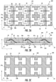
- FIG. 2A shows a top view of a package assembly 200 with a top major surface 22 of the mold encapsulation 22 after step 13 of the process 100 of FIG. 1 .
- a plurality of leads 23 are provided as part of a lead frame 25.
- a die 20 is deposited on each of the leads 23 on a die surface 27a of the leads (e.g., top surface, as shown in FIG. 2B ).
- a given die 20a is deposited on a given first lead 23a of the plurality of leads 23 and may be electrically connected to an adjacent lead (e.g., second lead 23b), of the plurality of leads.
- the electrical connections may be implemented using wires 21, such as a given wire 21a, bonded to the given die 20a deposited on a die surface 27 of the first lead 23a, the given wire 21a connecting to a die surface 27a of a second lead 23b.
- the plurality of dies 20 are deposited on respective leads 23 and are electrically connected to adjacent leads 23 using wire bonds.
- Portions of mold encapsulation 22 are shown in FIG. 2A , though it will be understood that the mold encapsulation 22 covers the lead frame and associated components, as seen from the cross-sectional view shown in FIG. 2B .
- the mold encapsulation 22 may be partially or fully opaque and may be of a given color (e.g., black, grey, etc) such that the lead frame and associated components may not be visible from a top view.
- the mold encapsulation 22 is shown as transparent for illustrative purposes, such that the lead frame and associated components are visible in FIG. 2A
- Leads 23a and 23b, die 20a, and wire 20a are referenced herein for exemplary purposes; however, one of ordinary skill in the art would understand that the same description generally applies for each of the plurality of leads 23, dies 20, and wires 21.
- FIG. 2B shows a cross-sectional view of the package assembly 200 of FIG. 2A , after step 13 of the process 100 of FIG. 1 .
- the plurality of leads 23 e.g., first lead 23a and second lead 23b
- the plurality of dies 20 are deposited onto the leads 23 (e.g., 23a and 23b) and a given die 20a is deposited on a first lead (e.g., 23a), of the plurality of leads 23, may be electrically connected to a second lead (e.g., 23b), of the plurality of leads using electrical connections using wires (e.g., wire 21), as disclosed herein.
- a plurality of dies 20 are deposited on respective leads 23 (e.g., 23a) and are electrically connected to adjacent leads (e.g., 23b) using wires 21.
- mold encapsulation 22 encapsulates the dies 20, plurality of leads 23 and may be provided between the space between adjacent leads (e.g., between lead 23a and lead 23b). Further, the mold encapsulation 22 also encapsulates other components such as wires 21 (e.g., wire 21a).
- FIG. 2C shows a bottom view of the package assembly 200 of FIGS. 2A and 2B , after step 13 of the process 100 of FIG. 1 .
- a plurality of leads 23 e.g., leads 23a and 23b
- FIG. 2C shows the plating surface 27b (e.g., bottom surface) of leads 23a and 23b which may be adjacent to each other in an X direction.
- leads 23 that are adjacent to each other in a Y direction may be independent from each other during the semiconductor package fabrication, as disclosed herein.
- a bottom surface of the plurality of leads 23 of the lead frame may be plated with a first electrical plating 30.
- the plating surface 27b of the plurality of leads 23 may be the surface of the plurality of leads 23 that is opposite from the surface of the plurality of leads 23 that is bonded to the wires 21 deposited at step 11.
- the plating surface 27b of the plurality of leads 23 is the surface of the leads that is not covered by the molding material.
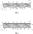
- a first electrical plating 30 may be applied by an electroplating process, at step 14 of the process 100 of FIG. 1 , as shown in FIG. 3 .
- the first electrical plating 30 may include one or more layers of a metal, such as tin or a tin alloy, plated on the plating surface 27b of the leads 23 and may protect the plating surface 27b of the leads 23 from oxidation and may also provide a wettable surface for soldering.
- the electroplating process may include depositing a conductive plating material that covers the plating surface (e.g., bottom surface) of the plurality of leads 23 of the lead frame 25 and allows for solder to adhere to the leads 23.
- a first electrical plating 30 material may be deposited on the exposed plating surfaces 27b (e.g., exposed bottom surfaces) of the leads 23.
- the lead frame 25 may be dipped in a bath and the lead frame 25 may be electrically coupled to the cathode of an electrolytic plating device (not shown).
- the anode of the electrolytic plating device may be coupled to the plating material, which is also dipped in the bath.
- An electrical current may be applied to the lead frame which causes the plating material to be deposited on the plating surface 27b (e.g., bottom surface) of the plurality of leads 23 so that, for example, the plating surface 27b of leads 23a and 23b are plated with the plating material.
- the first electrical plating 30 material may be any of a variety of plating materials, such as tin, gold, palladium, or silver.
- step 14 of the process 100 of FIG. 1 one of two processes may be taken, as shown in FIG. 1 .
- a first process - not an embodiment of the invention - is described at steps 15, 16, 18, and 19 of FIG. 1 and illustrated in FIGS. 4-8
- a second process - in accordance with the invention - is described at steps 17, 18, and 19 of FIG. 1 and illustrated at FIGS. 9-11 .
- top taping and saw singulation are performed as further described herein.
- step 15, top taping and saw singulation, of the process 100 of FIG. 1 may be taken after applying the first electrical plating 30 to the bottom exposed surfaces of the leads 23 (e.g., leads 23a and 23b of FIG. 3 ) at step 14 of the process 100.
- a first connecting film 40 may be applied to the top major surface 22a of the mold encapsulation 22.
- the connecting film 40 may be applied over a plurality of the leads 23 (e.g., leads 23a and 23b).
- the connecting film 40 may be any applicable film that attaches to the top major surface 22a of the mold encapsulation 22.
- the connecting film 40 may attach to the top major surface of the mold encapsulation 22 using any applicable adhesive material.
- Step 15 of the process 100 of FIG. 1 includes a singulation process.
- the singulation process at step 15 may be implemented using an applicable cutting device and/or technique such as, without limitation, a saw having a saw blade, or a laser cutter, a plasma cutter, or a water jet cutter, or any other acceptable cutting device and/or technique as known to those of skill in the art.
- the singulation process at step 15 may include making one or more cuts through the first electrical plating 30 on the plating surface 27b (e.g., bottom surface) of the plurality of leads 23 through the top major surface 22a of the mold encapsulation 22 to create one or more channels 50.
- the channels 50 may each expose lead sidewalls 55 and 56 on each side of each of the channels. As shown in FIGS.
- the lead frame 25 may be singulated into individual semiconductor die packages 80.
- the singulation process may include making a first series of parallel cuts 51a along a first direction (e.g., an X direction) cutting through the bottom major surface 22b (e.g., opposed major surface) of the mold encapsulation 22 opposite of the connecting film 40 to a depth up to the connecting film 40 or a portion of the connecting film 40.
- the first series of parallel cuts 51a may also cut through a portion of the lead frame 25 that is between adjacent leads 23 in the vertical direction (e.g., through lead connectors 28).
- lead connectors 28 may connect two adjacent leads and may be part of a lead frame (e.g., lead frame 25) itself or may be formed from one or more other materials.
- this first series of parallel cuts 51a only cut through the area between adjacent leads 23 (e.g., leads arranged above or below each other in the Y direction if viewing the package assembly 200 from a top view), and do not cut through the leads 23.
- the singulation process may further include making a second series of parallel cuts 51b along a second direction (e.g., a Y-direction), the second direction substantially perpendicular to the first direction, the second series of parallel cuts cutting through the plating surface 27b (e.g., bottom surface) of each of the plurality of leads 23, and the electrical plating 30 of each of the plurality of leads 23, and the mold encapsulation 22 to a depth up to the connecting film 40 or a portion of the connecting film 40 to create a channel 50 exposing a first lead sidewall 55 and a second lead sidewall 56 of each of the plurality of leads 23.
- a second direction e.g., a Y-direction
- the first and second series of parallel cuts 51a and 51b may be made at a depth not fully through the connecting film 40 shown in FIG. 4 and FIGS. 5A-C , to allow the packages to remain as a single assembly for additional handling in subsequent steps.
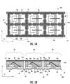
- FIG. 5A shows a top view of a package assembly 200 at step 15 of process 100 of FIG 1 .
- a plurality of cuts 51 e.g., 51a and 51b
- the top view shown in FIG. 5A is a top view from below connecting film 40 (not shown in FIG. 5A ).
- the plurality of cuts may include a series of parallel cuts 51a in the X direction (e.g., from a left side to a right side of the package assembly 200 shown in FIG. 5A ), as well a series of parallel cuts 51b in the Y direction, as indicated by the axis provided in FIG. 5A .
- the series of parallel cuts in the X direction 51a may cut through the bottom major surface 22b (e.g., opposed major surface) of the mold encapsulation 22 opposite of the connecting film 40 (shown in corresponding FIG. 5B ) to a depth up to the connecting film 40 or a portion of the connecting film 40.
- the leads 23 in the package assembly 200 are configured such that adjacent leads (e.g., 23a and 23b) in the X direction are connected by wires 21, and adjacent leads 23 in the Y direction may be connected by lead connectors 28 or may be independent of each other during fabrication of semiconductor die packages, as disclosed herein. It will be noted that the cuts 51a and 51b are shown in the top view of FIG.
- the cuts 51b in the Y direction create channels 50 (as shown in FIG. 5B ) that cut through each of the plurality of leads 23 (e.g., leads 23a and 23b) whereas the cuts 51a in the X direction may not cut through the plurality of leads 23 but rather separate adjacent leads in the Y direction from each other by cutting through the mold encapsulation 22 and/or lead connectors 28.
- FIG. 5B shows a cross-section view of the package assembly 200 of FIG. 5A , during step 15 of the process 100 of FIG. 1 .
- FIG. 5B shows a series of parallel cuts 51b made in the Y direction to create a plurality of channels 50.
- the series of parallel cuts 51b in the Y direction cut through the first electrical plating 30 on the plating surface 27b (e.g., bottom surface) of the plurality of leads 23 (e.g., leads 23a and 23b), through the plurality of leads 23, and through the mold encapsulation 22.
- FIG. 5B shows the channels 50 extending partially into the connecting film 40, though it will be understood that, according to an embodiment, the channels 50 may be formed up to, but not through a portion of the connecting film 40.
- the connecting film 40 is contiguous over the major top surface 22a of the mold encapsulation 22 across multiple leads 23.
- the connecting film 40 may have properties (e.g., strength, rigidity, elasticity, etc.) that enable the connecting film 40 to maintain the plurality of semiconductor die packages 80 of the package assembly 200 that are separated by the channels 50, to remain as part of a single unit connected by the connecting film 40.
- the connecting film 40 may enable the plurality of semiconductor die packages 80 of the package assembly 200 plus the plurality of channels 50 to have a width, in an X direction, that is substantially equal to the width of the package assembly 200 before the plurality of cuts at step 15 of process 100 (e.g., the width of the package assembly 200 prior to step 15, as shown in FIG. 4 ).
- the channels 50 expose lead sidewalls 55 and 56 of each of the plurality of leads 23 (e.g., leads 23a and 23b).
- the lead sidewalls 55 and 56 are created during the formation of the channels 50 such that the formation of the channels 50 cuts through each of the plurality of leads 23 (e.g., leads 23a and 23b) to expose two lead sidewalls 55 and 56 of each of the plurality of leads 23.
- the lead sidewalls 55 and 56 correspond to the portions of the leads that face the respective channels 50.
- the channels 50 are created between a first portion 24a and second portion 24b of each of the plurality of leads 23.
- the first portion 24a preferably includes a wire 21 (e.g., wire 21a) bonded to the die surface 27a of the first portion 24a of the plurality of leads 23 and the second portion 24b preferably includes a die 21 (e.g., die 20a).
- each semiconductor die package 80 of the package assembly 200 includes a second portion 24b of a first lead 23a, including die 20a, and a first portion 24a of a second lead 23b, including wire 21a bonded to a die surface 27a of the first portion 24a of the second lead 23b.
- FIG. 5C shows a bottom view of the package assembly 200 of FIGs. 5A and 5B , at step 15 of the process 100 of FIG. 1 .
- the plurality of cuts 51 include a series of parallel cuts 51a in the X direction (e.g., from a left side to a right side of the package assembly 200 shown in FIG. 5C ), as well a series of parallel cuts 51b in the Y direction (e.g., from a top to a bottom of the package assembly 200 shown in FIG. 5C ).
- the series of parallel cuts in the X direction cut through the bottom major surface 22b (e.g., opposed major surface) of the mold encapsulation 22 opposite of the connecting film 40 (shown in corresponding FIG.
- the cuts 51b in the Y direction create channels 50 (as shown in FIG. 5B ) that cut through each of the plurality of leads 23 (e.g., leads 23a and 23b) whereas the cuts 51a in the X direction do not cut through the plurality of leads 23 but rather separate adjacent leads 23 in the Y direction from each other by cutting through the mold encapsulation 22 and/or lead connectors 28.
- the first series of parallel cuts 51a may also cut through a portion of the lead frame 25 that is between adjacent leads 23 in the vertical direction (e.g., if the lead connectors 28 are part of the lead frame 25).
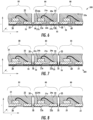
- a conductive film 60 is applied to the bottom of the semiconductor die packages 80 of the package assembly 200 that are separated by channels 50.
- the conductive film 60 may be applied while the connecting film 40 of FIGS. 4 and 5B is attached to the top major surface 22a of the mold encapsulation 22 such that the semiconductor die packages 80 of the package assembly 200 maintain their position and/or structure while the conductive film 60 is applied.
- the connecting film 40 of FIGS. 4 and 5B may be removed at step 16 of process 100 such that the semiconductor die packages 80 of the package assembly 200 may be connected to each other by the conductive film 60.
- the conductive film 60 may have properties (e.g., strength, rigidity, elasticity, etc.) that enable the conductive film 60 to maintain the plurality semiconductor die packages 80 of the package assembly 200 that are separated by the channels 50, to remain as part of a single unit connected by the conductive film 60.
- the conductive film 60 may enable the plurality of semiconductor die packages 80 of the package assembly 200 plus the plurality of channels 50 to have a width, in an X direction, that is substantially equal to the width of the package assembly 200 before the removal of the connecting film 40 at step 16 of process 100 (e.g., the width of the package assembly 200 prior to step 16, as shown in FIG. 5B ).
- the conductive film 60 may be made from any applicable material that conducts electricity such that an electrical path is maintained between segments of the package assembly 200 separate by channels 50.
- the conductive film 60 may be made from or may include metal or metal alloys. It will be noted that although conductive film 60 is described herein, the conductive film 60 may also be a connecting film.
- the conductive film 60 is preferably applied to a bottom of the semiconductor die packages 80 of the package assembly 200, as shown in FIG. 6 .
- the conductive film 60 is more preferably applied to one or more of the bottom major surface 22b of the mold encapsulation 22 and/or the first electrical plating 30 on the plating surface 27b (e.g., bottom surface) of the plurality of leads 23.
- the lead sidewalls 55 and 56 of the plurality of leads 23 may be plated at step 18 of the process 100 of FIG. 1 .
- a second electrical plating 70 may be applied by an electroplating process, at step 18 of the process 100 of FIG. 1 .
- the second electrical plating 70 may be one or more layers of a metal such as tin or a tin alloy that plated on the lead sidewalls and may protect the lead sidewalls from oxidation and may also provide a wettable surface for soldering.
- the electroplating process at step 18 may include depositing a conductive plating material to cover the exposed surface of lead sidewalls 55 and 56 e.g., through the channels 50).
- the semiconductor die packages 80 of the package assembly 200 connected by the conductive film 60, may be dipped in a bath and may be electrically coupled to the cathode of an electrolytic plating device.
- the anode of the electrolytic plating device may be coupled to the plating material, which is also dipped in the bath.
- An electrical current may be applied to the semiconductor die packages 80 of the package assembly 200, connected by the conductive film 60, which causes the plating material to be deposited on the exposed surface of the lead sidewalls 55 and 56 of the plurality of leads so that, for example, the exposed surface of the lead sidewalls of leads 23a and 23b are plated with the plating material (electrical plating 70).
- the plating material electrical plating 70.
- each portion 24a and 24b of a lead e.g., a first portion and second portion 24a and 24b of lead 23b
- electrical plating e.g., first electrical plating 30 on a plating surface and second electrical plating on a sidewall surface
- the conductive film 60 is removed, as shown in FIG. 8 .
- a plurality of semiconductor die packages 80 corresponding to each of the plurality of package assembly 200 segments of FIG. 7 remain.
- Each of the plurality of semiconductor die packages 80 include a first portion 24a of a lead 23 (e.g., lead 23b), a die 20 (e.g., die 20a) deposited over a second portion 24b of a lead 23 (e.g., lead 23a), a wire 21 (e.g., wire 21a) electrically connecting the die 20 (e.g., die 20a) to a first portion 24a of the lead 23 (e.g., a first portion 24a of lead 23b).
- a lead 23 e.g., lead 23b
- a die 20 e.g., die 20a
- a wire 21 e.g., wire 21a
- each of the portions 24a and 24b of leads 23 for each of the plurality of semiconductor die packages 80 include electrical plating material on the plating surfaces 27b (e.g., bottom surfaces) of the portions of the leads as well as the sidewall surfaces 55 and 56 of each of the leads 23.
- step 17 bottom taping and saw singulation are performed as an alternative to steps 15 and 16 of process 100 of FIG. 1 .
- FIG. 9 shows an example of step 17 which includes applying a conductive film 90 to the bottom surface 202 of the package assembly 200 after step 14 of the process 100 of FIG. 1 .
- step 17 follows step 14 of the process 100 of FIG 1 such that step 17 is performed after the first electrical plating 30 is applied to the plating surface 27b (e.g., bottom surface) of the leads 23.
- the conductive film 90 applied at step 17 is attached to both of the bottom major surface 22b of the mold encapsulation 22 and the first electrical plating 30 on the plating surface 27b (e.g., bottom surface) of the plurality of leads 23.
- step 17 includes a singulation process, such as a saw singulation process described in relation to step 15 of process 100 of FIG. 1 .
- FIG. 10A shows a cross-section view of the package assembly 200 and
- FIG. 10B shows a top view of the package assembly 200 at step 17.
- the singulation process at step 17 may be implemented using an applicable cutting device and/or technique such as a saw having a saw blade, or a laser cutter, a plasma cutter, or a water jet cutter, or any other acceptable cutting device and/or technique as known to those of skill in the art.
- the singulation process at step 17 may include making one or more cuts 52 (e.g., 52a and/or 52b) through the top major surface 22a of the mold encapsulation 22 through the plurality of leads 23 (e.g., leads 23a an 23b) to create one or more channels 50.
- the channels 50 may each include exposed lead sidewalls 55 and 56 on each side of each of the channels.
- the package assembly 200 may be singulated into individual semiconductor die packages 80 connected only by the conductive film 90.
- the singulation process at step 17 may include making a first series of parallel cuts 52a along a first direction (e.g., an X direction) cutting through the top major surface 22a of the mold encapsulation 22 opposite of the conductive film 90 to a depth down to the conductive film 90 or a portion of the conductive film 90.
- this first series of parallel cuts 52a only cut through lead connectors 28, as shown in FIG. 5A , and the area between adjacent electrically unconnected leads (e.g., leads arranged above or below each other if viewing the package assembly 200 from a top view, as shown in FIG. 10B ), and do not cut through the leads 23.
- the first series of parallel cuts 52a may also cut through a portion of the lead frame 25, such as the lead connectors 28, that is between adjacent leads 23 in the vertical direction.
- the singulation process may further include making a second series of parallel cuts 52b along a second direction (e.g., a Y direction), the second direction substantially perpendicular to the first direction, the second series of parallel cuts 52b cutting through the top major surface 22a of the mold encapsulation 22 surface, down through plurality of leads 23, and through the first electrical plating 30 of each of the plurality of leads to a depth up to the conductive film 90 or a portion of the conductive film 90 to create channels 50 exposing a first lead sidewall 55 and a second lead sidewall 56 of each of the plurality of leads 23.
- conductive film 90 may also be a connecting film.
- the first and/or second series of parallel step cuts 52a and/or 52b between the semiconductor die packages 80 that form the channels 50 result in exposed sidewalls that will form wettable flanks.
- the first and second series of parallel cuts 52a and 52b may be made at a depth that does not extend fully through the conductive film 90, to allow the semiconductor die packages 80 to remain as a single assembly for additional handling in subsequent steps.
- the conductive film 90 may have properties (e.g., strength, rigidity, elasticity, etc.) that enable the conductive film 90 to maintain the plurality of semiconductor die packages 80 of the package assembly 200, that are separated by the channels 50, to remain as part of a single unit connected by the conductive film 90.
- the conductive film 90 may enable the semiconductor die packages 80 of the package assembly 200 plus the plurality of channels 50 to have a width, in an X direction, that is substantially equal to the width of the package assembly 200 before the singulation at step 17 (e.g., the width of the package assembly 200 prior to step 17, as shown in FIG. 3 ).
- the conductive film 90 may be made from any applicable material that conducts electricity such that an electrical path is maintained between segments of the package assembly 200 separated by channels 50.
- the conductive film 90 may be made from or may include metal or metal alloys.
- steps 18 and 19 may be performed after the application of conductive film 90 and the plurality of cuts 52a and/or 52b to create channels 50 of step 17.
- the lead sidewalls 55 and 56 of the plurality of leads 23 may be plated at step 18 of the process 100 of FIG. 1 .
- a second electrical plating 70 may be applied by an electroplating process, at step 18 of the process 100 of FIG. 1 .
- the second electrical plating 70 may be one or more layers of a metal such as tin or a tin alloy that is plated on the lead sidewalls 55 and 56 and may protect the lead sidewalls 55 and 56 from oxidation and may also provide a wettable surface for soldering.
- the electroplating process at step 18 may include depositing a conductive plating material (not shown) to cover the exposed surface of lead sidewalls (e.g., through the channels 50).
- the semiconductor die package 80 of the package assembly 200 connected by the conductive film 90, may be dipped in a bath and may be electrically coupled to the cathode of an electrolytic plating device (not shown).
- the anode of the electrolytic plating device may be coupled to the plating material, which is also dipped in the bath.
- An electrical current may be applied to the lead frame 25 of the package assembly 200, connected by the conductive film 90, which causes the plating material to be deposited on the exposed surfaces of the lead sidewalls 55 and 56 of the plurality of leads so that, for example, the exposed surface of the lead sidewalls 55 and 56 leads 23 are plated with the plating material (i.e., resulting in electrical plating 70).
- the plating material i.e., resulting in electrical plating 70.
- each portion 24a and 24b of a lead 23 e.g., a first portion 24a and second portion 24b of lead 23b
- electrical plating e.g., first electrical plating 30 on a plating surface 27b (e.g., bottom surface) and second electrical plating 70 on a lead sidewalls 55, 56.
- the conductive film 90 is removed, as shown in FIG. 8 .
- the plurality of semiconductor die packages 80, of package assembly 200 of FIG. 11 remain.
- Each of the plurality of semiconductor die packages 80 include a first portion 24a of a lead 23 (e.g., a second portion of lead 23b shown in the middle semiconductor die package 80 of FIG.
- each of the portions of leads 23 for each of the plurality of semiconductor die packages 80 include electrical plating material on the plating surfaces 27b (e.g., electrical plating material 30) of the portions of the leads 23 as well as the lead sidewalls 55 and 56 (e.g., electrical plating material 70) of each of the leads 23.
- the electrical plating material (e.g., 30 and/or 70) may serve to mount a given semiconductor die package to a printed circuit board (PCB).
- leads 23a and 23b are shown and/or described herein, the techniques of the present disclosure are applicable to assembly packages having any configuration of leads and/or dies. Additionally, it is understood by one in the art that the same or similar techniques may be applied to provide QFN packages with wettable flanks as DFN packages with wettable flanks.
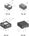
- FIGS. 12A and 12B show a DFN package with wettable flanks 250 with a first electrical plating material 30 on the bottom of two corresponding leads (not shown) as well as a second electrical plating 70 on the lead sidewalls (not shown) of the DFN package 250.
- the first plating material 30 and the second plating material 70 may be plated in accordance with the process 100 of FIG. 1 , as disclosed herein.
- a tie bar area 35 may also be plated (e.g., with second electrical plating 70).
- the tie bar area 35 may assist with, as disclosed herein, forming an electrical connection for current flow during electroplating (e.g., during the first electrical plating 30 and/or second electrical plating 70 such as, for example, in the absence of a conductive film 90).
- FIGS. 12C and 12D show a QFN package 260 with a first electrical plating material 30 on the bottom of corresponding leads (not shown) as well as a second electrical plating 70 on the lead sidewalls (not shown) of the QFN package 260.
- the first plating material 30 and the second plating material 70 may be plated in accordance with the process 100 of FIG. 1 , as disclosed herein.
- the process 100 of FIG. 1 provides a multi-step plating process to form semiconductor die package having wettable flanks.
- the process 100 provides for separate plating steps for plating different surfaces (e.g., plating surface or sidewalls) of semiconductor die packages.
- the separate plating steps may allow for a simplified plating process and may reduce the complexity of plating multiple surfaces at the same time. Further, the separate plating steps may allow for plating different surfaces (e.g., plating surface or sidewalls) with different plating material or different concentration of plating materials.
Landscapes
- Lead Frames For Integrated Circuits (AREA)
- Encapsulation Of And Coatings For Semiconductor Or Solid State Devices (AREA)
- Chemically Coating (AREA)
- Physics & Mathematics (AREA)
- Geometry (AREA)
Description
- Flat "no-leads' or "leadless" semiconductor die packages electrically and physically couple integrated circuit dies (or "dice") to printed circuit boards ("PCB") with flat leads and without through holes extending through a printed circuit board (PCB). Although these semiconductor die packages are referred to as "no-leads" or "leadless" packages, the term "leads" in the present disclosure is used to refer to the flat contact pads present on flat no-leads packages. These semiconductor die packages have no "leads" in the sense that there are no leads that extend past or beyond the outer periphery of the package. Flat no-leads packages may be classified as quad flat no-leads ("QFN") packages, having leads on all four sides of the package, and dual flat no-leads ("DFN") packages, having leads on two opposing sides. Within these semiconductor die packages, one or more integrated circuit dies is encapsulated within a non-conductive molding material. An electrically conductive lead frame, typically made of a metal like copper, is electrically coupled to internal components of the semiconductor die package and exposes leads externally that can be electrically coupled to a PCB. Improvements to flat no-leads packages are constantly being made.
- Leadless semiconductor die packages have several advantages over packages having leads extending beyond a perimeter of the package. Such semiconductor die packages may have a low profile as compared to other types of semiconductor die packages. Such semiconductor die packages may take up less space and thereby have a smaller "footprint" on a printed circuit board than conventional packages having leads extending beyond the perimeter of the semiconductor die packages. Such leadless semiconductor die packages may also have better thermal performance as compared to packages having leads extending beyond the perimeter of the package.
- An issue within the relevant industry as it concerns QFN and DFN packages relates to the inspection of the solder connections to the leads of the packages. In order to ensure proper solder connections to QFN and DFN packages, it is necessary to inspect the connections. These inspections can be performed by x-ray, for example, or by automated optical inspection (AOI). Automated optical inspection (AOI) systems are used to inspect, for example, semiconductor devices and printed circuit boards (PCBs), for defects. QFN and DFN packages can allow for AOI, which is less costly than x-ray inspections, if the leads are oriented in such a manner that the portions of the sides or "flanks" of the leads are wettable by solder, such as by having solder wick up the sides or sidewalls of the exposed leads.
- A method of making Flat No-Lead Packages with plated lead surfaces is described in
US 2016/181122 A1 . In this method, the packages are mounted on a dicing tape and singulated, after which a conductive plate is applied and cut surface portions of the leads are plated in an electroplating bath. - Conventional lead wettable devices may be formed by a step cutting process which requires multiple surfaces to be plated at the same time with the same platable material. Plating multiple surfaces at the same time may be complicated and may not allow targeted plating for specific surfaces.
- There is therefore the need for an efficient method of manufacturing a semiconductor die packages having wettable flanks.
- The invention is defined by claim 1.
- The method for fabricating a semiconductor die package from a package assembly includes a lead frame including at least a first lead and a second lead, the first and second leads each having a top surface and a bottom surface, a first integrated circuit die provided on the top surface of the first lead, a second integrated circuit die provided on the top surface of the second lead, and a mold encapsulation surrounding at least portions of the lead frame and at least portions of the first integrated circuit die and the second integrated circuit die, the mold encapsulation having a top major surface and a bottom major surface. A bottom surface of the first lead and a bottom surface of the second lead are plated with a first electrical plating. A conductive film is applied to connect the bottom surface of the first lead and the bottom surface of the second lead. A cut is made to create a channel through the mold encapsulation, the second lead, and the first electrical plating on the bottom surface of the second lead, the channel exposing a first lead sidewall and a second lead sidewall of the second lead. The first lead sidewall and the second lead sidewall are platted, through the channel, with a second electrical plating and the conductive film is removed.
- A more detailed understanding can be had from the following description, given by way of example in conjunction with the accompanying drawings wherein:
-
FIG. 1 is a flow diagram of an illustrative method for forming wettable flanks on a semiconductor die package from a package assembly, according to an example; -
FIG. 2A is a top view of a package assembly illustrating a lead frame with dies in a mold encapsulation, according to an example; -
FIG. 2B is a cross-sectional view of the package assembly ofFIG. 2A , according to an example; -
FIG. 2C is a bottom view of the package assembly ofFIG. 2A , according to an example; -
FIG. 3 is a cross-sectional view of a package assembly with bottom plating, according to an example; -
FIG. 4 is a cross-sectional view of the package assembly with a film applied on a top surface, according to an example; -
FIG. 5A is a top view of package assembly illustrating the cuts and cutting pattern that create channels within the package assembly, according to an example; -
FIG. 5B is a cross-sectional view of the package assembly ofFIG. 5A , according to an example; -
FIG. 5C is a bottom view of the package assembly ofFIG. 5A , according to an example; -
FIG. 6 is a cross-sectional view of a package assembly after cutting with a conductive film attached, according to an example; -
FIG. 7 is a cross-sectional view of the package assembly with a conductive film and sidewall electric plating, according to an example; -
FIG. 8 is a cross-sectional view of finished semiconductor die packages with bottom and sidewall electric plating, according to an example; -
FIG. 9 is a cross-sectional view of an embodiment in accordance with the invention of a package assembly with bottom electric plating and a conductive film, according to an example; -
FIG. 10A is a cross-sectional view of the package assembly after cutting to create channels within the package assembly, according to an example; -
FIG. 10B is a top view of the package assembly after cutting to create channels within the package assembly, according to an example; -
FIG. 11 is a cross-sectional view of the package assembly with a conductive film and sidewall electric plating; -
FIG. 12A is a perspective view of a bottom side of a DFN package with bottom and sidewall plating, according to an example; -
FIG. 12B is perspective view of a top side of the DFN package ofFIG. 12A with bottom and sidewall plating, according to an example; -
FIG. 12C is a perspective view of a bottom side of a QFN package with bottom and sidewall plating, according to an example; and -
FIG. 12D is a perspective view of the top side of the QFN package ofFIG. 12C with bottom and sidewall plating, according to an example. - Certain terminology is used in the following description for convenience only and is not limiting. The words "right," "left," "top," and "bottom" designate directions in the drawings to which reference is made. However, it will be understood that such orientation-based terms are for reference only and that the embodiments may be implemented in different directions such that such terms may be applied as adjusted based on such respective different directions. The words "a" and "one," as used in the claims and in the corresponding portions of the specification, are defined as including one or more of the referenced item unless specifically stated otherwise. This terminology includes the words above specifically mentioned, derivatives thereof, and words of similar import. The phrase "at least one" followed by a list of two or more items, such as "A, B, or C," means any individual one of A, B or C as well as any combination thereof.
- The description provided herein is to enable those skilled in the art to make and use the described embodiments set forth.
- Techniques are disclosed herein for forming bottom and sidewall wettable flanks on semiconductor die packages, and, preferably, DFN and/or QFN semiconductor die packages. The techniques include a package assembly having multiple non-singulated packages. The package assembly includes a lead frame having dies and other internal package components (e.g., wire bonds) coupled thereto. The dies and other components form different regions of non-singulated packages, as further disclosed herein. The dies and other components are encapsulated within a mold encapsulation (also referred to as a "molding," "mold," "encapsulation," "encapsulation material," "mold encapsulation material", or other similar term herein). The mold encapsulation may be non-conductive and may cover all or most of the package components but may leave exposed certain electrical contact pads (referred to herein as "leads," including a "first lead" and a "second lead") and, possibly, thermal contact pads (referred to herein as "die paddles") as well as other components as disclosed herein. The mold encapsulation may include a top major surface that is opposite to the bottom surface of the plurality of leads and a bottom major surface that is adjacent and substantially parallel to the bottom surface of the plurality of the leads. The lead frame provides a continuous electrical connection between one end of the package assembly and the other, and between the various exposed leads and die paddles of the semiconductor die packages. Elements such as wire bonds or tie bars may assist with forming the electrical connection. This electrical connection may be used for current flow during electroplating (e.g., a first electrical plating), which may be a step that occurs in the process for forming bottom and sidewall wettable flanks on DFN and/or QFN packages.
-
FIG. 1 shows a flow diagram of aprocess 100 for forming a semiconductor die packages from a package assembly, according to an aspect of the present invention. Theprocess 100 ofFIG. 1 is discussed in conjunction withFIGS. 2-11 , which illustrate stages of apackage assembly 200 as theprocess 100 proceeds. Alead frame 25, as referenced herein, may be cut from a lead frame material such as a sheet of copper. A lead frame assembly, as referenced herein, may be thelead frame 25 having a plurality of leads 23. As shown inFIGS. 2A-2C , theleads 23 may be etched into portions of thelead frame 25. - The
package assembly 200 is shown with atop surface 201 and abottom surface 202, as indicated inFIGS. 2A- 2C . At step 10 of theprocess 100, a plurality ofdie 20 are deposited on and bonded to a corresponding plurality ofleads 23 of alead frame 25 that are part of the lead frame assembly. The lead frame assembly may includemultiple leads 23 integrated into a single part or unit. The lead frame assembly may include any metal alloy. A plurality of semiconductor die packages may be formed in an array of die packages in thepackage assembly 200, which are then cut (e.g., singulated) into individual semiconductor die packages. Each semiconductor die package may include a second portion (e.g., 24b as described inFIG. 5B ) of a lead 23 (e.g., 23a) that is attached to adie 20, a first portion (e.g., 25a as described inFIG. 5B ) of a lead 23 (e.g., 23b) that is electrically connected to the die 20 (e.g., bywire 21 or a tie-bar (not shown)), andmold encapsulation 22. A singulated semiconductor die package may be a semiconductor die package that is separated from one or more other semiconductor die packages in the package assembly, as further described herein. - At step 10, one or more of the integrated circuit dies, which are referred to herein as "dies," for simplicity, may be deposited on the
leads 23 of thelead frame 25. Atstep 11, other components, such aswires 21, conductive clips (elements within the semiconductor die package that couple the die(s) to one or more leads), or other elements are deposited to form a plurality of semiconductor die packages. - At
step 12, a portion of thelead frame 25 is taped, and amold encapsulation 22 is deposited around thelead frame 25 and other components of the semiconductor die packages. Notably, a bottom portion of the lead frame that faces away from the wire bonds formed bywires 21 deposited atstep 11 may be taped to prevent the mold encapsulation deposited atstep 12 to extend past the base of thelead frame 25 such as through gaps between two or more leads 23 in thelead frame 25. Themold encapsulation 22 may provide a physical and electrical barrier for the components of the package. Themold encapsulation 22 may be a silica-filled resin, a ceramic, a halide-free material, or other protective encapsulation material, or a combination thereof. Themold encapsulation 22 may be formed by molding thermosetting materials in a process where a plastic is softened by heat and pressure in a transfer chamber, then forced at high pressure through suitable sprues, runners, and gates into a closed mold for final curing. The mold encapsulant may also be formed by using a liquid which may be heated to form a solid by curing in a UV or ambient atmosphere, or by using a solid that is heated to form a liquid and then cooled to form a solid mold. Atstep 13, thelead frame 25 may be de-taped, afterstep 12, and one or more markings (not shown) may be applied to the lead frame assembly. The markings may include one or more fiducial marks which are marks detectable by a machine that allow the machine to align itself for cutting. Afterstep 13, apackage assembly 200 is provided that includes multiple non-singulated semiconductor die packages with package components (e.g., dies, the lead frame, and the components that couple the dies to the lead frame) encapsulated within amolding material 22. -
FIG. 2A shows a top view of apackage assembly 200 with a topmajor surface 22 of themold encapsulation 22 afterstep 13 of theprocess 100 ofFIG. 1 . As shown inFIG. 2A , a plurality ofleads 23 are provided as part of alead frame 25. A die 20 is deposited on each of theleads 23 on adie surface 27a of the leads (e.g., top surface, as shown inFIG. 2B ). As shown inFIG. 2B , a givendie 20a is deposited on a givenfirst lead 23a of the plurality ofleads 23 and may be electrically connected to an adjacent lead (e.g.,second lead 23b), of the plurality of leads. The electrical connections may be implemented usingwires 21, such as a givenwire 21a, bonded to the givendie 20a deposited on a die surface 27 of thefirst lead 23a, the givenwire 21a connecting to adie surface 27a of asecond lead 23b. Similarly, the plurality of dies 20 are deposited onrespective leads 23 and are electrically connected toadjacent leads 23 using wire bonds. Portions ofmold encapsulation 22 are shown inFIG. 2A , though it will be understood that themold encapsulation 22 covers the lead frame and associated components, as seen from the cross-sectional view shown inFIG. 2B . In an embodiment, themold encapsulation 22 may be partially or fully opaque and may be of a given color (e.g., black, grey, etc) such that the lead frame and associated components may not be visible from a top view. However, it will be understood that in the top view, as shown inFIG. 2A , themold encapsulation 22 is shown as transparent for illustrative purposes, such that the lead frame and associated components are visible inFIG. 2A Leads 23a and 23b, die 20a, andwire 20a are referenced herein for exemplary purposes; however, one of ordinary skill in the art would understand that the same description generally applies for each of the plurality ofleads 23, dies 20, andwires 21. -
FIG. 2B shows a cross-sectional view of thepackage assembly 200 ofFIG. 2A , afterstep 13 of theprocess 100 ofFIG. 1 . As shown inFIG. 2B , the plurality of leads 23 (e.g.,first lead 23a and second lead 23b) are provided as part of alead frame 25. The plurality of dies 20 are deposited onto the leads 23 (e.g., 23a and 23b) and a givendie 20a is deposited on a first lead (e.g., 23a), of the plurality ofleads 23, may be electrically connected to a second lead (e.g., 23b), of the plurality of leads using electrical connections using wires (e.g., wire 21), as disclosed herein. Similarly, a plurality of dies 20 (e.g., die 20a) are deposited on respective leads 23 (e.g., 23a) and are electrically connected to adjacent leads (e.g., 23b) usingwires 21. As shown,mold encapsulation 22, encapsulates the dies 20, plurality ofleads 23 and may be provided between the space between adjacent leads (e.g., betweenlead 23a and lead 23b). Further, themold encapsulation 22 also encapsulates other components such as wires 21 (e.g.,wire 21a). -
FIG. 2C shows a bottom view of thepackage assembly 200 ofFIGS. 2A and 2B , afterstep 13 of theprocess 100 ofFIG. 1 . As shown inFIG. 2C , a plurality of leads 23 (e.g., leads 23a and 23b) may be arranged in an array configuration.FIG. 2C shows theplating surface 27b (e.g., bottom surface) ofleads FIG. 2C ) may be independent from each other during the semiconductor package fabrication, as disclosed herein. - At
step 14 of theprocess 100 ofFIG. 1 , a bottom surface of the plurality ofleads 23 of the lead frame may be plated with a firstelectrical plating 30. Theplating surface 27b of the plurality ofleads 23 may be the surface of the plurality ofleads 23 that is opposite from the surface of the plurality ofleads 23 that is bonded to thewires 21 deposited atstep 11. Notably, theplating surface 27b of the plurality ofleads 23 is the surface of the leads that is not covered by the molding material. - A first
electrical plating 30 may be applied by an electroplating process, atstep 14 of theprocess 100 ofFIG. 1 , as shown inFIG. 3 . The firstelectrical plating 30 may include one or more layers of a metal, such as tin or a tin alloy, plated on theplating surface 27b of theleads 23 and may protect theplating surface 27b of theleads 23 from oxidation and may also provide a wettable surface for soldering. The electroplating process may include depositing a conductive plating material that covers the plating surface (e.g., bottom surface) of the plurality ofleads 23 of thelead frame 25 and allows for solder to adhere to the leads 23. A firstelectrical plating 30 material may be deposited on the exposed platingsurfaces 27b (e.g., exposed bottom surfaces) of the leads 23. During the electroplating process ofstep 14, thelead frame 25 may be dipped in a bath and thelead frame 25 may be electrically coupled to the cathode of an electrolytic plating device (not shown). The anode of the electrolytic plating device may be coupled to the plating material, which is also dipped in the bath. An electrical current may be applied to the lead frame which causes the plating material to be deposited on theplating surface 27b (e.g., bottom surface) of the plurality ofleads 23 so that, for example, theplating surface 27b ofleads step 14, because only the plating surfaces 27b of theleads electrical plating 30. Notably, sidewalls 55 and 56, as further disclosed herein, of theleads electrical plating 30 material may be any of a variety of plating materials, such as tin, gold, palladium, or silver. - After
step 14 of theprocess 100 ofFIG. 1 , one of two processes may be taken, as shown inFIG. 1 . A first process - not an embodiment of the invention - is described atsteps FIG. 1 and illustrated inFIGS. 4-8 , and a second process - in accordance with the invention - is described atsteps FIG. 1 and illustrated atFIGS. 9-11 . - Referring to the first process (not an embodiment of the invention), at
step 15, top taping and saw singulation are performed as further described herein. - According to an embodiment,
step 15, top taping and saw singulation, of theprocess 100 ofFIG. 1 may be taken after applying the firstelectrical plating 30 to the bottom exposed surfaces of the leads 23 (e.g., leads 23a and 23b ofFIG. 3 ) atstep 14 of theprocess 100. Atstep 15, as shown inFIG. 4 , a first connectingfilm 40 may be applied to the topmajor surface 22a of themold encapsulation 22. As shown, the connectingfilm 40 may be applied over a plurality of the leads 23 (e.g., leads 23a and 23b). The connectingfilm 40 may be any applicable film that attaches to the topmajor surface 22a of themold encapsulation 22. The connectingfilm 40 may attach to the top major surface of themold encapsulation 22 using any applicable adhesive material. -
Step 15 of theprocess 100 ofFIG. 1 includes a singulation process. The singulation process atstep 15 may be implemented using an applicable cutting device and/or technique such as, without limitation, a saw having a saw blade, or a laser cutter, a plasma cutter, or a water jet cutter, or any other acceptable cutting device and/or technique as known to those of skill in the art. The singulation process atstep 15 may include making one or more cuts through the firstelectrical plating 30 on theplating surface 27b (e.g., bottom surface) of the plurality ofleads 23 through the topmajor surface 22a of themold encapsulation 22 to create one ormore channels 50. Thechannels 50 may each exposelead sidewalls FIGS. 5A-5C , thelead frame 25 may be singulated into individual semiconductor die packages 80. The singulation process may include making a first series ofparallel cuts 51a along a first direction (e.g., an X direction) cutting through the bottommajor surface 22b (e.g., opposed major surface) of themold encapsulation 22 opposite of the connectingfilm 40 to a depth up to the connectingfilm 40 or a portion of the connectingfilm 40. The first series ofparallel cuts 51a may also cut through a portion of thelead frame 25 that is betweenadjacent leads 23 in the vertical direction (e.g., through lead connectors 28). As applied herein,lead connectors 28 may connect two adjacent leads and may be part of a lead frame (e.g., lead frame 25) itself or may be formed from one or more other materials. Notably, this first series ofparallel cuts 51a only cut through the area between adjacent leads 23 (e.g., leads arranged above or below each other in the Y direction if viewing thepackage assembly 200 from a top view), and do not cut through the leads 23. The singulation process may further include making a second series ofparallel cuts 51b along a second direction (e.g., a Y-direction), the second direction substantially perpendicular to the first direction, the second series of parallel cuts cutting through theplating surface 27b (e.g., bottom surface) of each of the plurality ofleads 23, and theelectrical plating 30 of each of the plurality ofleads 23, and themold encapsulation 22 to a depth up to the connectingfilm 40 or a portion of the connectingfilm 40 to create achannel 50 exposing afirst lead sidewall 55 and asecond lead sidewall 56 of each of the plurality of leads 23. - The first and/or second, series of
parallel step cuts packages 80 create sidewalls 55 and 56 where wettable flanks will be formed. The first and second series ofparallel cuts film 40 shown inFIG. 4 andFIGS. 5A-C , to allow the packages to remain as a single assembly for additional handling in subsequent steps. -
FIG. 5A shows a top view of apackage assembly 200 atstep 15 ofprocess 100 ofFIG 1 . As shown inFIG. 5A , a plurality of cuts 51 (e.g., 51a and 51b) may be made during a singulation process. The top view shown inFIG. 5A is a top view from below connecting film 40 (not shown inFIG. 5A ). The plurality of cuts may include a series ofparallel cuts 51a in the X direction (e.g., from a left side to a right side of thepackage assembly 200 shown inFIG. 5A ), as well a series ofparallel cuts 51b in the Y direction, as indicated by the axis provided inFIG. 5A . The series of parallel cuts in theX direction 51a may cut through the bottommajor surface 22b (e.g., opposed major surface) of themold encapsulation 22 opposite of the connecting film 40 (shown in correspondingFIG. 5B ) to a depth up to the connectingfilm 40 or a portion of the connectingfilm 40. Notably, according to the example shown inFIGS. 5A-C , theleads 23 in thepackage assembly 200 are configured such that adjacent leads (e.g., 23a and 23b) in the X direction are connected bywires 21, andadjacent leads 23 in the Y direction may be connected bylead connectors 28 or may be independent of each other during fabrication of semiconductor die packages, as disclosed herein. It will be noted that thecuts FIG. 5A are from below the connecting film 40 (not shown inFIG. 5A ) as thecuts 51 do not extend through the connectingfilm 40 that is above themold encapsulation 22 shown inFIG. 5A . Thecuts 51b in the Y direction create channels 50 (as shown inFIG. 5B ) that cut through each of the plurality of leads 23 (e.g., leads 23a and 23b) whereas thecuts 51a in the X direction may not cut through the plurality ofleads 23 but rather separate adjacent leads in the Y direction from each other by cutting through themold encapsulation 22 and/or leadconnectors 28. -
FIG. 5B shows a cross-section view of thepackage assembly 200 ofFIG. 5A , duringstep 15 of theprocess 100 ofFIG. 1 .FIG. 5B shows a series ofparallel cuts 51b made in the Y direction to create a plurality ofchannels 50. Notably, the series ofparallel cuts 51b in the Y direction cut through the firstelectrical plating 30 on theplating surface 27b (e.g., bottom surface) of the plurality of leads 23 (e.g., leads 23a and 23b), through the plurality ofleads 23, and through themold encapsulation 22.FIG. 5B shows thechannels 50 extending partially into the connectingfilm 40, though it will be understood that, according to an embodiment, thechannels 50 may be formed up to, but not through a portion of the connectingfilm 40. As shown inFIG. 5B , at least a portion of the connectingfilm 40 is contiguous over the majortop surface 22a of themold encapsulation 22 across multiple leads 23. Notably, the connectingfilm 40 may have properties (e.g., strength, rigidity, elasticity, etc.) that enable the connectingfilm 40 to maintain the plurality of semiconductor diepackages 80 of thepackage assembly 200 that are separated by thechannels 50, to remain as part of a single unit connected by the connectingfilm 40. For example, the connectingfilm 40 may enable the plurality of semiconductor diepackages 80 of thepackage assembly 200 plus the plurality ofchannels 50 to have a width, in an X direction, that is substantially equal to the width of thepackage assembly 200 before the plurality of cuts atstep 15 of process 100 (e.g., the width of thepackage assembly 200 prior to step 15, as shown inFIG. 4 ). - As shown in
FIG 5B , thechannels 50 expose lead sidewalls 55 and 56 of each of the plurality of leads 23 (e.g., leads 23a and 23b). The lead sidewalls 55 and 56 are created during the formation of thechannels 50 such that the formation of thechannels 50 cuts through each of the plurality of leads 23 (e.g., leads 23a and 23b) to expose twolead sidewalls respective channels 50. Notably, thechannels 50 are created between afirst portion 24a andsecond portion 24b of each of the plurality of leads 23. Thefirst portion 24a preferably includes a wire 21 (e.g.,wire 21a) bonded to thedie surface 27a of thefirst portion 24a of the plurality ofleads 23 and thesecond portion 24b preferably includes a die 21 (e.g., die 20a). As shown inFIG. 5B , for example, after the plurality ofcuts package 80 of thepackage assembly 200 includes asecond portion 24b of afirst lead 23a, includingdie 20a, and afirst portion 24a of asecond lead 23b, includingwire 21a bonded to adie surface 27a of thefirst portion 24a of thesecond lead 23b. -
FIG. 5C shows a bottom view of thepackage assembly 200 ofFIGs. 5A and 5B , atstep 15 of theprocess 100 ofFIG. 1 . As shown inFIG. 5C , the plurality ofcuts 51 include a series ofparallel cuts 51a in the X direction (e.g., from a left side to a right side of thepackage assembly 200 shown inFIG. 5C ), as well a series ofparallel cuts 51b in the Y direction (e.g., from a top to a bottom of thepackage assembly 200 shown inFIG. 5C ). The series of parallel cuts in the X direction cut through the bottommajor surface 22b (e.g., opposed major surface) of themold encapsulation 22 opposite of the connecting film 40 (shown in correspondingFIG. 5B ) to a depth up to the connectingfilm 40 or a portion of the connectingfilm 40. Thecuts 51b in the Y direction create channels 50 (as shown inFIG. 5B ) that cut through each of the plurality of leads 23 (e.g., leads 23a and 23b) whereas thecuts 51a in the X direction do not cut through the plurality ofleads 23 but rather separateadjacent leads 23 in the Y direction from each other by cutting through themold encapsulation 22 and/or leadconnectors 28. As disclosed herein, the first series ofparallel cuts 51a may also cut through a portion of thelead frame 25 that is betweenadjacent leads 23 in the vertical direction (e.g., if thelead connectors 28 are part of the lead frame 25). - At step 16 of the
process 100 ofFIG. 1 , as shown inFIG. 6 , aconductive film 60 is applied to the bottom of the semiconductor diepackages 80 of thepackage assembly 200 that are separated bychannels 50. Theconductive film 60 may be applied while the connectingfilm 40 ofFIGS. 4 and5B is attached to the topmajor surface 22a of themold encapsulation 22 such that the semiconductor diepackages 80 of thepackage assembly 200 maintain their position and/or structure while theconductive film 60 is applied. The connectingfilm 40 ofFIGS. 4 and5B may be removed at step 16 ofprocess 100 such that the semiconductor diepackages 80 of thepackage assembly 200 may be connected to each other by theconductive film 60. Notably, theconductive film 60 may have properties (e.g., strength, rigidity, elasticity, etc.) that enable theconductive film 60 to maintain the plurality semiconductor diepackages 80 of thepackage assembly 200 that are separated by thechannels 50, to remain as part of a single unit connected by theconductive film 60. For example, theconductive film 60 may enable the plurality of semiconductor diepackages 80 of thepackage assembly 200 plus the plurality ofchannels 50 to have a width, in an X direction, that is substantially equal to the width of thepackage assembly 200 before the removal of the connectingfilm 40 at step 16 of process 100 (e.g., the width of thepackage assembly 200 prior to step 16, as shown inFIG. 5B ). Theconductive film 60 may be made from any applicable material that conducts electricity such that an electrical path is maintained between segments of thepackage assembly 200 separate bychannels 50. For example, theconductive film 60 may be made from or may include metal or metal alloys. It will be noted that althoughconductive film 60 is described herein, theconductive film 60 may also be a connecting film. - The
conductive film 60 is preferably applied to a bottom of the semiconductor diepackages 80 of thepackage assembly 200, as shown inFIG. 6 . Theconductive film 60 is more preferably applied to one or more of the bottommajor surface 22b of themold encapsulation 22 and/or the firstelectrical plating 30 on theplating surface 27b (e.g., bottom surface) of the plurality of leads 23. - After applying the
conductive film 60 to the bottom of the semiconductor diepackages 80 of thepackage assembly 200 and removing the connectingfilm 40 from the top of the semiconductor diepackages 80 of thepackage assembly 200 at step 16, the lead sidewalls 55 and 56 of the plurality ofleads 23 may be plated atstep 18 of theprocess 100 ofFIG. 1 . As shown inFIG. 7 a secondelectrical plating 70 may be applied by an electroplating process, atstep 18 of theprocess 100 ofFIG. 1 . The secondelectrical plating 70 may be one or more layers of a metal such as tin or a tin alloy that plated on the lead sidewalls and may protect the lead sidewalls from oxidation and may also provide a wettable surface for soldering. The electroplating process atstep 18 may include depositing a conductive plating material to cover the exposed surface of lead sidewalls 55 and 56 e.g., through the channels 50). During the electroplating process ofstep 18, the semiconductor diepackages 80 of thepackage assembly 200, connected by theconductive film 60, may be dipped in a bath and may be electrically coupled to the cathode of an electrolytic plating device. The anode of the electrolytic plating device may be coupled to the plating material, which is also dipped in the bath. An electrical current may be applied to the semiconductor diepackages 80 of thepackage assembly 200, connected by theconductive film 60, which causes the plating material to be deposited on the exposed surface of the lead sidewalls 55 and 56 of the plurality of leads so that, for example, the exposed surface of the lead sidewalls ofleads step 18, because only thesidewalls leads electrical plating 70. Notably, after applying the secondelectrical plating 70 atstep 18, at least two surfaces of eachportion second portion electrical plating 30 on a plating surface and second electrical plating on a sidewall surface). - At
step 19 of theprocess 100 ofFIG. 1 , theconductive film 60 is removed, as shown inFIG. 8 . After removal of theconductive film 60 atstep 19, a plurality of semiconductor diepackages 80 corresponding to each of the plurality ofpackage assembly 200 segments ofFIG. 7 remain. Each of the plurality of semiconductor diepackages 80 include afirst portion 24a of a lead 23 (e.g., lead 23b), a die 20 (e.g., die 20a) deposited over asecond portion 24b of a lead 23 (e.g., lead 23a), a wire 21 (e.g.,wire 21a) electrically connecting the die 20 (e.g., die 20a) to afirst portion 24a of the lead 23 (e.g., afirst portion 24a oflead 23b). Additionally, each of theportions leads 23 for each of the plurality of semiconductor diepackages 80 include electrical plating material on the plating surfaces 27b (e.g., bottom surfaces) of the portions of the leads as well as the sidewall surfaces 55 and 56 of each of the leads 23. - Referring to the second process in accordance with the invention, at
step 17 bottom taping and saw singulation are performed as an alternative tosteps 15 and 16 ofprocess 100 ofFIG. 1 .FIG. 9 shows an example ofstep 17 which includes applying aconductive film 90 to thebottom surface 202 of thepackage assembly 200 afterstep 14 of theprocess 100 ofFIG. 1 . To clarify, as shown inFIG. 1 ,step 17 followsstep 14 of theprocess 100 ofFIG 1 such thatstep 17 is performed after the firstelectrical plating 30 is applied to theplating surface 27b (e.g., bottom surface) of the leads 23. Theconductive film 90 applied atstep 17 is attached to both of the bottommajor surface 22b of themold encapsulation 22 and the firstelectrical plating 30 on theplating surface 27b (e.g., bottom surface) of the plurality of leads 23. - As shown in
FIGS. 10a and 10b ,step 17 includes a singulation process, such as a saw singulation process described in relation to step 15 ofprocess 100 ofFIG. 1 .FIG. 10A shows a cross-section view of thepackage assembly 200 andFIG. 10B shows a top view of thepackage assembly 200 atstep 17. The singulation process atstep 17 may be implemented using an applicable cutting device and/or technique such as a saw having a saw blade, or a laser cutter, a plasma cutter, or a water jet cutter, or any other acceptable cutting device and/or technique as known to those of skill in the art. As further described herein, the singulation process atstep 17 may include making one or more cuts 52 (e.g., 52a and/or 52b) through the topmajor surface 22a of themold encapsulation 22 through the plurality of leads 23 (e.g., leads 23a an 23b) to create one ormore channels 50. Thechannels 50 may each include exposed lead sidewalls 55 and 56 on each side of each of the channels. Thepackage assembly 200 may be singulated into individual semiconductor diepackages 80 connected only by theconductive film 90. The singulation process atstep 17 may include making a first series ofparallel cuts 52a along a first direction (e.g., an X direction) cutting through the topmajor surface 22a of themold encapsulation 22 opposite of theconductive film 90 to a depth down to theconductive film 90 or a portion of theconductive film 90. Notably, this first series ofparallel cuts 52a only cut throughlead connectors 28, as shown inFIG. 5A , and the area between adjacent electrically unconnected leads (e.g., leads arranged above or below each other if viewing thepackage assembly 200 from a top view, as shown inFIG. 10B ), and do not cut through the leads 23. The first series ofparallel cuts 52a may also cut through a portion of thelead frame 25, such as thelead connectors 28, that is betweenadjacent leads 23 in the vertical direction. The singulation process may further include making a second series ofparallel cuts 52b along a second direction (e.g., a Y direction), the second direction substantially perpendicular to the first direction, the second series ofparallel cuts 52b cutting through the topmajor surface 22a of themold encapsulation 22 surface, down through plurality ofleads 23, and through the firstelectrical plating 30 of each of the plurality of leads to a depth up to theconductive film 90 or a portion of theconductive film 90 to createchannels 50 exposing afirst lead sidewall 55 and asecond lead sidewall 56 of each of the plurality of leads 23. It will be noted that althoughconductive film 90 is described herein, theconductive film 90 may also be a connecting film. - The first and/or second series of
parallel step cuts 52a and/or 52b between the semiconductor diepackages 80 that form thechannels 50 result in exposed sidewalls that will form wettable flanks. The first and second series ofparallel cuts conductive film 90, to allow the semiconductor diepackages 80 to remain as a single assembly for additional handling in subsequent steps. Notably, theconductive film 90 may have properties (e.g., strength, rigidity, elasticity, etc.) that enable theconductive film 90 to maintain the plurality of semiconductor diepackages 80 of thepackage assembly 200, that are separated by thechannels 50, to remain as part of a single unit connected by theconductive film 90. For example, theconductive film 90 may enable the semiconductor diepackages 80 of thepackage assembly 200 plus the plurality ofchannels 50 to have a width, in an X direction, that is substantially equal to the width of thepackage assembly 200 before the singulation at step 17 (e.g., the width of thepackage assembly 200 prior to step 17, as shown inFIG. 3 ). Theconductive film 90 may be made from any applicable material that conducts electricity such that an electrical path is maintained between segments of thepackage assembly 200 separated bychannels 50. For example, theconductive film 90 may be made from or may include metal or metal alloys. - As described herein, steps 18 and 19 may be performed after the application of
conductive film 90 and the plurality ofcuts 52a and/or 52b to createchannels 50 ofstep 17. Notably the lead sidewalls 55 and 56 of the plurality of leads 23 (e.g., the surfaces facing channels 50) may be plated atstep 18 of theprocess 100 ofFIG. 1 . As shown inFIG. 11 a secondelectrical plating 70 may be applied by an electroplating process, atstep 18 of theprocess 100 ofFIG. 1 . The secondelectrical plating 70 may be one or more layers of a metal such as tin or a tin alloy that is plated on the lead sidewalls 55 and 56 and may protect the lead sidewalls 55 and 56 from oxidation and may also provide a wettable surface for soldering. The electroplating process atstep 18 may include depositing a conductive plating material (not shown) to cover the exposed surface of lead sidewalls (e.g., through the channels 50). During the electroplating process ofstep 18, thesemiconductor die package 80 of thepackage assembly 200, connected by theconductive film 90, may be dipped in a bath and may be electrically coupled to the cathode of an electrolytic plating device (not shown). The anode of the electrolytic plating device may be coupled to the plating material, which is also dipped in the bath. An electrical current may be applied to thelead frame 25 of thepackage assembly 200, connected by theconductive film 90, which causes the plating material to be deposited on the exposed surfaces of the lead sidewalls 55 and 56 of the plurality of leads so that, for example, the exposed surface of the lead sidewalls 55 and 56 leads 23 are plated with the plating material (i.e., resulting in electrical plating 70). Atstep 18, because only the surfaces of the lead sidewalls 55 and 56 are exposed, only these surfaces are plated by the secondelectrical plating 70. Notably, after applying the secondelectrical plating 70 atstep 18, at least two surfaces of eachportion first portion 24a andsecond portion 24b of lead 23b) are covered by electrical plating (e.g., firstelectrical plating 30 on aplating surface 27b (e.g., bottom surface) and secondelectrical plating 70 on alead sidewalls 55, 56). - At
step 19 of theprocess 100 ofFIG. 1 , theconductive film 90 is removed, as shown inFIG. 8 . As shown, after removal of theconductive film 90 atstep 19, only the plurality of semiconductor diepackages 80, ofpackage assembly 200 ofFIG. 11 , remain. Each of the plurality of semiconductor diepackages 80 include afirst portion 24a of a lead 23 (e.g., a second portion oflead 23b shown in the middle semiconductor diepackage 80 ofFIG. 8 ), a die 20 (e.g., die 20a) bonded to asecond portion 24b of thelead 23a, a wire 21 (e.g.,wire 21a) electrically connecting the die 20 (e.g., die 20a) to thefirst portion 24a of a lead 23 (e.g., afirst portion 24a oflead 23b). Additionally, each of the portions ofleads 23 for each of the plurality of semiconductor diepackages 80 include electrical plating material on the plating surfaces 27b (e.g., electrical plating material 30) of the portions of theleads 23 as well as the lead sidewalls 55 and 56 (e.g., electrical plating material 70) of each of the leads 23. The electrical plating material (e.g., 30 and/or 70) may serve to mount a given semiconductor die package to a printed circuit board (PCB). - Although a specific number and configuration of leads (e.g., leads 23a and 23b) is shown and/or described herein, the techniques of the present disclosure are applicable to assembly packages having any configuration of leads and/or dies. Additionally, it is understood by one in the art that the same or similar techniques may be applied to provide QFN packages with wettable flanks as DFN packages with wettable flanks.
-
FIGS. 12A and 12B show a DFN package withwettable flanks 250 with a firstelectrical plating material 30 on the bottom of two corresponding leads (not shown) as well as a secondelectrical plating 70 on the lead sidewalls (not shown) of theDFN package 250. Thefirst plating material 30 and thesecond plating material 70 may be plated in accordance with theprocess 100 ofFIG. 1 , as disclosed herein. Additionally, as shown inFIGS. 12A atie bar area 35 may also be plated (e.g., with second electrical plating 70). Thetie bar area 35 may assist with, as disclosed herein, forming an electrical connection for current flow during electroplating (e.g., during the firstelectrical plating 30 and/or secondelectrical plating 70 such as, for example, in the absence of a conductive film 90). -
FIGS. 12C and 12D show aQFN package 260 with a firstelectrical plating material 30 on the bottom of corresponding leads (not shown) as well as a secondelectrical plating 70 on the lead sidewalls (not shown) of theQFN package 260. Thefirst plating material 30 and thesecond plating material 70 may be plated in accordance with theprocess 100 ofFIG. 1 , as disclosed herein. - The
process 100 ofFIG. 1 , as described herein, provides a multi-step plating process to form semiconductor die package having wettable flanks. Theprocess 100 provides for separate plating steps for plating different surfaces (e.g., plating surface or sidewalls) of semiconductor die packages. The separate plating steps may allow for a simplified plating process and may reduce the complexity of plating multiple surfaces at the same time. Further, the separate plating steps may allow for plating different surfaces (e.g., plating surface or sidewalls) with different plating material or different concentration of plating materials.
Claims (4)
- A method for fabricating a semiconductor package (80) from a package assembly (200) comprising:providing a lead frame (25) comprising at least a first lead (23a) and a second lead (23b), the first and second leads (23a, 23b) each having a top surface (27a) and a bottom surface (27b), a first integrated circuit die (20) on the top surface (27a) of the first lead (23a), and a second integrated circuit die (20) on the top surface (27a) of the second lead (23b);encapsulating at least portions of the lead frame (25) and at least portions of the first integrated circuit die (20) and the second integrated circuit die (20) in a mold encapsulation (22), the mold encapsulation having a top major surface (22a) and a bottom major surface (22b);plating the bottom surface (27b) of the first lead (23a) and the bottom surface (27b) of the second lead (23b) with a first electrical plating (30);applying a conductive film (90) to connect the bottom surface (27b) of the first lead (23a) and the bottom surface (27b) of the second lead (23b);cutting through the mold encapsulation (22), the second lead (23b), and the first electrical plating (30) on the bottom surface (27b) of the second lead (23b) to create a channel (50), the channel (50) exposing a first lead sidewall (55) and a second lead sidewall (56) of the second lead (23b);plating, through the channel (50), the first lead sidewall (55) and the second lead sidewall (56) with a second electrical plating (70); andremoving the conductive film (90),characterized in thatthe cutting is carried out while the conductive film (90) is connected to the bottom surface (27b) of the first and second leads (23a, 23b).
- The method of claim 1, wherein making the cut (52) further comprises making a partial cut through the conductive film (90).
- The method of claim 1, whereinthe channel (50) separates the second lead (23b) into two portions (24a, 24b);the first integrated circuit die (20) on the first lead (23a) is electrically connected to a first portion (24a) of the two portions of the second lead (23b) by a bonding wire (21a); andthe second integrated circuit (20) is on a second portion (24b) of the two portions of the second lead (23b).
- The method of claim 1, wherein plating the bottom surface (27b) of the first lead (23a) and the bottom surface (27b) of the second lead (23b) comprises:dipping the package assembly (200) in a solution;electrically coupling a power source to the lead frame (25) and to a plating material in the solution; andapplying current to the lead frame (25) via the power source.
Applications Claiming Priority (2)
| Application Number | Priority Date | Filing Date | Title |
|---|---|---|---|
| CN201911347346.8A CN113035721A (en) | 2019-12-24 | 2019-12-24 | Packaging process for plating conductive film on side wall |
| PCT/US2020/017131 WO2021133419A1 (en) | 2019-12-24 | 2020-02-07 | Packaging process for side-wall plating with a conductive film |
Publications (3)
| Publication Number | Publication Date |
|---|---|
| EP3871250A1 EP3871250A1 (en) | 2021-09-01 |
| EP3871250A4 EP3871250A4 (en) | 2022-04-27 |
| EP3871250B1 true EP3871250B1 (en) | 2025-03-26 |
Family
ID=76451696
Family Applications (1)
| Application Number | Title | Priority Date | Filing Date |
|---|---|---|---|
| EP20848928.6A Active EP3871250B1 (en) | 2019-12-24 | 2020-02-07 | Packaging process for side-wall plating with a conductive film |
Country Status (8)
| Country | Link |
|---|---|
| US (2) | US11450534B2 (en) |
| EP (1) | EP3871250B1 (en) |
| JP (1) | JP7545957B2 (en) |
| KR (1) | KR20220120444A (en) |
| CN (1) | CN113035721A (en) |
| IL (1) | IL280220B2 (en) |
| TW (1) | TWI860327B (en) |
| WO (1) | WO2021133419A1 (en) |
Families Citing this family (9)
| Publication number | Priority date | Publication date | Assignee | Title |
|---|---|---|---|---|
| CN113035721A (en) * | 2019-12-24 | 2021-06-25 | 维谢综合半导体有限责任公司 | Packaging process for plating conductive film on side wall |
| CN113035722A (en) | 2019-12-24 | 2021-06-25 | 维谢综合半导体有限责任公司 | Packaging process for plating with selective molding |
| US20230298982A1 (en) * | 2022-03-15 | 2023-09-21 | Texas Instruments Incorporated | Electronic device with improved board level reliability |
| EP4300552A1 (en) * | 2022-06-29 | 2024-01-03 | Nexperia B.V. | A method of manufacturing semiconductor package assembly and a semiconductor package assembly manufactured using this method |
| US12538812B2 (en) * | 2023-02-07 | 2026-01-27 | Semiconductor Components Industries, Llc | Semiconductor packages with wettable flanks and related methods |
| CN116387198B (en) * | 2023-04-07 | 2024-11-01 | 上海聚跃检测技术有限公司 | A cutting and separation method for QFN packaged chip |
| US12456674B2 (en) | 2023-05-23 | 2025-10-28 | Littelfuse, Inc. | Leadframeless electrically isolated power semiconductor package |
| US20250046621A1 (en) * | 2023-07-31 | 2025-02-06 | Texas Instruments Incorporated | Ic package with immersion tin on flank |
| EP4657521A1 (en) * | 2024-05-29 | 2025-12-03 | Nexperia B.V. | A method of fabricating a semiconductor integrated circuits package |
Family Cites Families (107)
| Publication number | Priority date | Publication date | Assignee | Title |
|---|---|---|---|---|
| US6219908B1 (en) | 1991-06-04 | 2001-04-24 | Micron Technology, Inc. | Method and apparatus for manufacturing known good semiconductor die |
| US5801432A (en) | 1992-06-04 | 1998-09-01 | Lsi Logic Corporation | Electronic system using multi-layer tab tape semiconductor device having distinct signal, power and ground planes |
| EP1213755A3 (en) | 1994-03-18 | 2005-05-25 | Hitachi Chemical Co., Ltd. | Fabrication process of semiconductor package and semiconductor package |
| US6001671A (en) | 1996-04-18 | 1999-12-14 | Tessera, Inc. | Methods for manufacturing a semiconductor package having a sacrificial layer |
| US6498099B1 (en) | 1998-06-10 | 2002-12-24 | Asat Ltd. | Leadless plastic chip carrier with etch back pad singulation |
| US6238952B1 (en) | 2000-02-29 | 2001-05-29 | Advanced Semiconductor Engineering, Inc. | Low-pin-count chip package and manufacturing method thereof |
| JP2001326295A (en) | 2000-05-15 | 2001-11-22 | Rohm Co Ltd | Semiconductor device and semiconductor device manufacturing frame |
| US6400004B1 (en) | 2000-08-17 | 2002-06-04 | Advanced Semiconductor Engineering, Inc. | Leadless semiconductor package |
| TW488042B (en) | 2000-11-30 | 2002-05-21 | Siliconware Precision Industries Co Ltd | Quad flat non-leaded package and its leadframe |
| JP4308528B2 (en) | 2001-01-31 | 2009-08-05 | 株式会社ルネサステクノロジ | Semiconductor device and manufacturing method thereof |
| JP4034073B2 (en) | 2001-05-11 | 2008-01-16 | 株式会社ルネサステクノロジ | Manufacturing method of semiconductor device |
| TW498443B (en) * | 2001-06-21 | 2002-08-11 | Advanced Semiconductor Eng | Singulation method for manufacturing multiple lead-free semiconductor packages |
| US20030006055A1 (en) | 2001-07-05 | 2003-01-09 | Walsin Advanced Electronics Ltd | Semiconductor package for fixed surface mounting |
| US6891276B1 (en) | 2002-01-09 | 2005-05-10 | Bridge Semiconductor Corporation | Semiconductor package device |
| US6989295B1 (en) | 2002-01-09 | 2006-01-24 | Bridge Semiconductor Corporation | Method of making a semiconductor package device that includes an insulative housing with first and second housing portions |
| US6608366B1 (en) | 2002-04-15 | 2003-08-19 | Harry J. Fogelson | Lead frame with plated end leads |
| US8236612B2 (en) | 2002-04-29 | 2012-08-07 | Unisem (Mauritius) Holdings Limited | Partially patterned lead frames and methods of making and using the same in semiconductor packaging |
| EP1514306A2 (en) | 2002-06-06 | 2005-03-16 | Philips Intellectual Property & Standards GmbH | Quad flat non-leaded package comprising a semiconductor device |
| US6872599B1 (en) | 2002-12-10 | 2005-03-29 | National Semiconductor Corporation | Enhanced solder joint strength and ease of inspection of leadless leadframe package (LLP) |
| TWI235440B (en) | 2004-03-31 | 2005-07-01 | Advanced Semiconductor Eng | Method for making leadless semiconductor package |
| US7087461B2 (en) * | 2004-08-11 | 2006-08-08 | Advanced Semiconductor Engineering, Inc. | Process and lead frame for making leadless semiconductor packages |
| US7645635B2 (en) | 2004-08-16 | 2010-01-12 | Micron Technology, Inc. | Frame structure and semiconductor attach process for use therewith for fabrication of image sensor packages and the like, and resulting packages |
| WO2006122467A1 (en) * | 2005-04-07 | 2006-11-23 | Jiangsu Changjiang Electronics Technology Co., Ltd. | A packaging substrate with flat bumps for ic or discrete device and method of manufacturing the same |
| US7087462B1 (en) * | 2005-06-07 | 2006-08-08 | Advanced Semiconductor Engineering, Inc. | Method for forming leadless semiconductor packages |
| WO2006134534A1 (en) | 2005-06-15 | 2006-12-21 | Nxp B.V. | Layer sequence and method of manufacturing a layer sequence |
| JP2008545274A (en) | 2005-06-30 | 2008-12-11 | フェアチャイルド セミコンダクター コーポレイション | Semiconductor die package and manufacturing method thereof |
| US8053872B1 (en) * | 2007-06-25 | 2011-11-08 | Rf Micro Devices, Inc. | Integrated shield for a no-lead semiconductor device package |
| TW200737479A (en) | 2005-11-03 | 2007-10-01 | Koninkl Philips Electronics Nv | Surface treatments for contact pads used in semiconductor chip packages and methods of providing such surface treatments |
| US8437141B2 (en) | 2005-11-28 | 2013-05-07 | Nxp B.V. | Device comprising a substrate including an electronic contact, and transponder |
| WO2007060631A1 (en) | 2005-11-28 | 2007-05-31 | Nxp B.V. | A method of producing a transponder and a transponder |
| US7943431B2 (en) | 2005-12-02 | 2011-05-17 | Unisem (Mauritius) Holdings Limited | Leadless semiconductor package and method of manufacture |
| US7816186B2 (en) | 2006-03-14 | 2010-10-19 | Unisem (Mauritius) Holdings Limited | Method for making QFN package with power and ground rings |
| US8436460B1 (en) | 2007-05-04 | 2013-05-07 | Cypress Semiconductor Corporation | Multiple die paddle leadframe and semiconductor device package |
| US7576415B2 (en) * | 2007-06-15 | 2009-08-18 | Advanced Semiconductor Engineering, Inc. | EMI shielded semiconductor package |
| WO2009072052A1 (en) | 2007-12-06 | 2009-06-11 | Nxp B.V. | Semiconductor device and wafer with a test structure and method for assessing adhesion of under-bump metallization |
| DE202008005708U1 (en) | 2008-04-24 | 2008-07-10 | Vishay Semiconductor Gmbh | Surface-mountable electronic component |
| WO2009133499A2 (en) | 2008-04-28 | 2009-11-05 | Nxp B.V. | Microfluidic pump |
| WO2009144672A1 (en) | 2008-05-30 | 2009-12-03 | Nxp B.V. | Sensor for determining humidity |
| US20100044850A1 (en) * | 2008-08-21 | 2010-02-25 | Advanced Semiconductor Engineering, Inc. | Advanced quad flat non-leaded package structure and manufacturing method thereof |
| WO2010032192A1 (en) | 2008-09-16 | 2010-03-25 | Nxp B.V. | Electric component with under-bump metallization and integrated confinement structure |
| US8071427B2 (en) | 2009-01-29 | 2011-12-06 | Semiconductor Components Industries, Llc | Method for manufacturing a semiconductor component and structure therefor |
| US10163766B2 (en) | 2016-11-21 | 2018-12-25 | Semiconductor Components Industries, Llc | Methods of forming leadless semiconductor packages with plated leadframes and wettable flanks |
| EP2337068A1 (en) | 2009-12-18 | 2011-06-22 | Nxp B.V. | Pre-soldered leadless package |
| EP2361000A1 (en) | 2010-02-11 | 2011-08-24 | Nxp B.V. | Leadless chip package mounting method and carrier |
| US8329509B2 (en) | 2010-04-01 | 2012-12-11 | Freescale Semiconductor, Inc. | Packaging process to create wettable lead flank during board assembly |
| EP2400534A1 (en) | 2010-06-22 | 2011-12-28 | Nxp B.V. | Packaged semiconductor device having improved locking properties |
| US9418919B2 (en) | 2010-07-29 | 2016-08-16 | Nxp B.V. | Leadless chip carrier having improved mountability |
| US8017447B1 (en) | 2010-08-03 | 2011-09-13 | Linear Technology Corporation | Laser process for side plating of terminals |
| US8642461B2 (en) * | 2010-08-09 | 2014-02-04 | Maxim Integrated Products, Inc. | Side wettable plating for semiconductor chip package |
| JP2012074517A (en) * | 2010-09-28 | 2012-04-12 | Seiko Instruments Inc | Semiconductor device manufacturing method and plating jig |
| CN103155136B (en) | 2010-09-29 | 2015-03-04 | Nxp股份有限公司 | Singulation of IC packages |
| US8076181B1 (en) | 2010-10-22 | 2011-12-13 | Linear Technology Corporation | Lead plating technique for singulated IC packages |
| TWI397964B (en) | 2011-01-19 | 2013-06-01 | 宇芯(毛里求斯)控股有限公司 | Partially patterned lead frame and method of making and using same in semiconductor package |
| US8969136B2 (en) * | 2011-03-25 | 2015-03-03 | Stats Chippac Ltd. | Integrated circuit packaging system for electromagnetic interference shielding and method of manufacture thereof |
| CN102789994B (en) | 2011-05-18 | 2016-08-10 | 飞思卡尔半导体公司 | The wettable semiconductor device in side |
| TWI458113B (en) | 2012-05-04 | 2014-10-21 | 台灣典範半導體股份有限公司 | Proximity sensor and its manufacturing method |
| US9397031B2 (en) | 2012-06-11 | 2016-07-19 | Utac Thai Limited | Post-mold for semiconductor package having exposed traces |
| EP2677540A1 (en) | 2012-06-19 | 2013-12-25 | Nxp B.V. | Electronic device and method of manufacturing the same |
| EP2677306B1 (en) | 2012-06-19 | 2017-11-29 | Nxp B.V. | Integrated circuit with ion sensitive sensor and manufacturing method |
| EP2677307B1 (en) | 2012-06-21 | 2016-05-11 | Nxp B.V. | Integrated circuit with sensors and manufacturing method |
| EP2693465A1 (en) | 2012-07-31 | 2014-02-05 | Nxp B.V. | Electronic device and method of manufacturing such device |
| US8884413B2 (en) | 2012-08-31 | 2014-11-11 | Freescale Semiconductor, Inc. | Leadframes, air-cavity packages, and electronic devices with offset vent holes, and methods of their manufacture |
| US9070669B2 (en) | 2012-11-09 | 2015-06-30 | Freescale Semiconductor, Inc. | Wettable lead ends on a flat-pack no-lead microelectronic package |
| US8535982B1 (en) | 2012-11-29 | 2013-09-17 | Freescale Semiconductor, Inc. | Providing an automatic optical inspection feature for solder joints on semiconductor packages |
| JP6030970B2 (en) | 2013-02-12 | 2016-11-24 | エスアイアイ・セミコンダクタ株式会社 | Resin-sealed semiconductor device and manufacturing method thereof |
| US20140357022A1 (en) | 2013-06-04 | 2014-12-04 | Cambridge Silicon Radio Limited | A qfn with wettable flank |
| US9287200B2 (en) | 2013-06-27 | 2016-03-15 | Freescale Semiconductor, Inc. | Packaged semiconductor device |
| US9012268B2 (en) * | 2013-06-28 | 2015-04-21 | Stmicroelectronics, Inc. | Leadless packages and method of manufacturing same |
| US9538659B2 (en) | 2013-08-21 | 2017-01-03 | Nxp Usa, Inc. | Solder wettable flanges and devices and systems incorporating solder wettable flanges |
| US9379071B2 (en) | 2014-04-17 | 2016-06-28 | Nxp B.V. | Single inline no-lead semiconductor package |
| US9472528B2 (en) | 2014-06-05 | 2016-10-18 | Freescale Semiconductor, Inc. | Integrated electronic package and method of fabrication |
| US9281284B2 (en) | 2014-06-20 | 2016-03-08 | Freescale Semiconductor Inc. | System-in-packages having vertically-interconnected leaded components and methods for the fabrication thereof |
| US20160005679A1 (en) | 2014-07-02 | 2016-01-07 | Nxp B.V. | Exposed die quad flat no-leads (qfn) package |
| EP2980845B1 (en) | 2014-08-01 | 2019-11-27 | Nexperia B.V. | A leadless semiconductor package and method |
| WO2016043697A1 (en) | 2014-09-15 | 2016-03-24 | Intel Corporation | Methods to form high density through-mold interconnections |
| US9257393B1 (en) | 2014-09-29 | 2016-02-09 | Freescale Semiconductor Inc. | Fan-out wafer level packages containing embedded ground plane interconnect structures and methods for the fabrication thereof |
| US9425130B2 (en) | 2014-10-29 | 2016-08-23 | Nxp B.V. | Package with multiple I/O side-solderable terminals |
| US20160148876A1 (en) | 2014-11-20 | 2016-05-26 | Microchip Technology Incorporated | Flat no-leads package with improved contact pins |
| US9673150B2 (en) | 2014-12-16 | 2017-06-06 | Nxp Usa, Inc. | EMI/RFI shielding for semiconductor device packages |
| CN105895611B (en) | 2014-12-17 | 2019-07-12 | 恩智浦美国有限公司 | With wettable side without lead quad flat semiconductor packages |
| US11348806B2 (en) * | 2014-12-23 | 2022-05-31 | Texas Instruments Incorporated | Making a flat no-lead package with exposed electroplated side lead surfaces |
| US10020380B2 (en) | 2015-01-23 | 2018-07-10 | Alpha And Omega Semiconductor Incorporated | Power device with high aspect ratio trench contacts and submicron pitches between trenches |
| EP3051592A1 (en) | 2015-01-27 | 2016-08-03 | Nxp B.V. | Semiconductor device |
| US9966326B2 (en) | 2015-03-16 | 2018-05-08 | Unisem (M) Berhad | Lead frames with wettable flanks |
| US9704823B2 (en) | 2015-03-21 | 2017-07-11 | Nxp B.V. | Reduction of defects in wafer level chip scale package (WLCSP) devices |
| JP2016219520A (en) * | 2015-05-18 | 2016-12-22 | Towa株式会社 | Semiconductor device and manufacturing method thereof |
| US9461009B1 (en) | 2015-05-27 | 2016-10-04 | Freescale Semiconductor, Inc. | Method and apparatus for assembling a semiconductor package |
| US9391007B1 (en) | 2015-06-22 | 2016-07-12 | Nxp B.V. | Built-up lead frame QFN and DFN packages and method of making thereof |
| US9640463B2 (en) | 2015-06-22 | 2017-05-02 | Nexperia B.V. | Built-up lead frame package and method of making thereof |
| GB2543514B (en) * | 2015-10-20 | 2020-04-01 | Ecorenew Dmcc | A Method for Preserving a Mark on a Metallic Workpiece |
| CN105225972B (en) * | 2015-10-22 | 2017-09-26 | 长电科技(滁州)有限公司 | A kind of preparation method of semiconductor package |
| CN105513976B (en) * | 2015-12-02 | 2018-04-17 | 上海凯虹电子有限公司 | Method for packaging semiconductor, packaging body and encapsulation unit |
| US10930581B2 (en) | 2016-05-19 | 2021-02-23 | Stmicroelectronics S.R.L. | Semiconductor package with wettable flank |
| US10256168B2 (en) | 2016-06-12 | 2019-04-09 | Nexperia B.V. | Semiconductor device and lead frame therefor |
| EP3261115A1 (en) | 2016-06-23 | 2017-12-27 | Nxp B.V. | Chip scale semiconductor package and method of manufacturing the same |
| US10083866B2 (en) | 2016-07-27 | 2018-09-25 | Texas Instruments Incorporated | Sawn leadless package having wettable flank leads |
| US10410941B2 (en) | 2016-09-08 | 2019-09-10 | Nexperia B.V. | Wafer level semiconductor device with wettable flanks |
| US20180102287A1 (en) | 2016-10-06 | 2018-04-12 | Nexperia B.V. | Leadframe-less surface mount semiconductor device |
| US9974174B1 (en) | 2016-10-26 | 2018-05-15 | Nxp Usa, Inc. | Package to board interconnect structure with built-in reference plane structure |
| US9847283B1 (en) | 2016-11-06 | 2017-12-19 | Nexperia B.V. | Semiconductor device with wettable corner leads |
| US9935079B1 (en) | 2016-12-08 | 2018-04-03 | Nxp Usa, Inc. | Laser sintered interconnections between die |
| US10079198B1 (en) | 2017-05-31 | 2018-09-18 | Stmicroelectronics, Inc. | QFN pre-molded leadframe having a solder wettable sidewall on each lead |
| TWM566910U (en) | 2018-05-04 | 2018-09-11 | 長華科技股份有限公司 | Preformed lead frame with tin-viewing groove with maximum viewing angle and packaging component thereof |
| US12224232B2 (en) | 2019-03-08 | 2025-02-11 | Siliconix Incorporated | Semiconductor package having side wall plating |
| IL285950B2 (en) | 2019-03-08 | 2025-07-01 | Siliconix Incorporated | Semiconductor package with coating on the side walls |
| CN113035721A (en) * | 2019-12-24 | 2021-06-25 | 维谢综合半导体有限责任公司 | Packaging process for plating conductive film on side wall |
| CN113035722A (en) | 2019-12-24 | 2021-06-25 | 维谢综合半导体有限责任公司 | Packaging process for plating with selective molding |
-
2019
- 2019-12-24 CN CN201911347346.8A patent/CN113035721A/en active Pending
-
2020
- 2020-02-07 WO PCT/US2020/017131 patent/WO2021133419A1/en not_active Ceased
- 2020-02-07 EP EP20848928.6A patent/EP3871250B1/en active Active
- 2020-02-07 US US17/059,074 patent/US11450534B2/en active Active
- 2020-02-07 JP JP2021507844A patent/JP7545957B2/en active Active
- 2020-02-07 KR KR1020217003735A patent/KR20220120444A/en not_active Ceased
- 2020-02-07 IL IL280220A patent/IL280220B2/en unknown
- 2020-02-10 TW TW109104058A patent/TWI860327B/en active
-
2022
- 2022-09-19 US US17/947,673 patent/US11876003B2/en active Active
Also Published As
| Publication number | Publication date |
|---|---|
| JP2023509239A (en) | 2023-03-08 |
| KR20220120444A (en) | 2022-08-30 |
| US11450534B2 (en) | 2022-09-20 |
| IL280220A (en) | 2021-06-30 |
| IL280220B2 (en) | 2023-11-01 |
| EP3871250A1 (en) | 2021-09-01 |
| CN113035721A (en) | 2021-06-25 |
| US20230019610A1 (en) | 2023-01-19 |
| WO2021133419A1 (en) | 2021-07-01 |
| TW202125652A (en) | 2021-07-01 |
| TWI860327B (en) | 2024-11-01 |
| US11876003B2 (en) | 2024-01-16 |
| IL280220B1 (en) | 2023-07-01 |
| EP3871250A4 (en) | 2022-04-27 |
| JP7545957B2 (en) | 2024-09-05 |
| US20210366729A1 (en) | 2021-11-25 |
Similar Documents
| Publication | Publication Date | Title |
|---|---|---|
| US11876003B2 (en) | Semiconductor package and packaging process for side-wall plating with a conductive film | |
| US11764075B2 (en) | Package assembly for plating with selective molding | |
| US12224232B2 (en) | Semiconductor package having side wall plating | |
| US12211704B2 (en) | Semiconductor package having side wall plating | |
| HK40055218A (en) | Packaging process for side-wall plating with a conductive film | |
| HK40055221A (en) | Packaging process for plating with selective molding | |
| US20150097278A1 (en) | Surface mount semiconductor device with additional bottom face contacts | |
| HK40063596A (en) | Semiconductor package having side wall plating | |
| HK40063592A (en) | Semiconductor package having side wall plating |
Legal Events
| Date | Code | Title | Description |
|---|---|---|---|
| STAA | Information on the status of an ep patent application or granted ep patent |
Free format text: STATUS: UNKNOWN |
|
| STAA | Information on the status of an ep patent application or granted ep patent |
Free format text: STATUS: THE INTERNATIONAL PUBLICATION HAS BEEN MADE |
|
| PUAI | Public reference made under article 153(3) epc to a published international application that has entered the european phase |
Free format text: ORIGINAL CODE: 0009012 |
|
| STAA | Information on the status of an ep patent application or granted ep patent |
Free format text: STATUS: REQUEST FOR EXAMINATION WAS MADE |
|
| 17P | Request for examination filed |
Effective date: 20210211 |
|
| AK | Designated contracting states |
Kind code of ref document: A1 Designated state(s): AL AT BE BG CH CY CZ DE DK EE ES FI FR GB GR HR HU IE IS IT LI LT LU LV MC MK MT NL NO PL PT RO RS SE SI SK SM TR |
|
| A4 | Supplementary search report drawn up and despatched |
Effective date: 20220328 |
|
| RIC1 | Information provided on ipc code assigned before grant |
Ipc: H01L 21/48 20060101ALI20220322BHEP Ipc: H01L 23/495 20060101ALI20220322BHEP Ipc: H01L 23/28 20060101ALI20220322BHEP Ipc: H01L 21/56 20060101AFI20220322BHEP |
|
| DAV | Request for validation of the european patent (deleted) | ||
| DAX | Request for extension of the european patent (deleted) | ||
| STAA | Information on the status of an ep patent application or granted ep patent |
Free format text: STATUS: EXAMINATION IS IN PROGRESS |
|
| 17Q | First examination report despatched |
Effective date: 20240318 |
|
| GRAP | Despatch of communication of intention to grant a patent |
Free format text: ORIGINAL CODE: EPIDOSNIGR1 |
|
| STAA | Information on the status of an ep patent application or granted ep patent |
Free format text: STATUS: GRANT OF PATENT IS INTENDED |
|
| RIC1 | Information provided on ipc code assigned before grant |
Ipc: H01L 21/683 20060101ALI20240902BHEP Ipc: H01L 21/48 20060101ALI20240902BHEP Ipc: H01L 23/495 20060101ALI20240902BHEP Ipc: H01L 23/28 20060101ALI20240902BHEP Ipc: H01L 21/56 20060101AFI20240902BHEP |
|
| INTG | Intention to grant announced |
Effective date: 20240913 |
|
| GRAS | Grant fee paid |
Free format text: ORIGINAL CODE: EPIDOSNIGR3 |
|
| GRAA | (expected) grant |
Free format text: ORIGINAL CODE: 0009210 |
|
| STAA | Information on the status of an ep patent application or granted ep patent |
Free format text: STATUS: THE PATENT HAS BEEN GRANTED |
|
| AK | Designated contracting states |
Kind code of ref document: B1 Designated state(s): AL AT BE BG CH CY CZ DE DK EE ES FI FR GB GR HR HU IE IS IT LI LT LU LV MC MK MT NL NO PL PT RO RS SE SI SK SM TR |
|
| REG | Reference to a national code |
Ref country code: GB Ref legal event code: FG4D |
|
| REG | Reference to a national code |
Ref country code: CH Ref legal event code: EP |
|
| REG | Reference to a national code |
Ref country code: DE Ref legal event code: R096 Ref document number: 602020048465 Country of ref document: DE |
|
| P01 | Opt-out of the competence of the unified patent court (upc) registered |
Free format text: CASE NUMBER: APP_13004/2025 Effective date: 20250317 |
|
| REG | Reference to a national code |
Ref country code: IE Ref legal event code: FG4D |
|
| PG25 | Lapsed in a contracting state [announced via postgrant information from national office to epo] |
Ref country code: RS Free format text: LAPSE BECAUSE OF FAILURE TO SUBMIT A TRANSLATION OF THE DESCRIPTION OR TO PAY THE FEE WITHIN THE PRESCRIBED TIME-LIMIT Effective date: 20250626 |
|
| PG25 | Lapsed in a contracting state [announced via postgrant information from national office to epo] |
Ref country code: FI Free format text: LAPSE BECAUSE OF FAILURE TO SUBMIT A TRANSLATION OF THE DESCRIPTION OR TO PAY THE FEE WITHIN THE PRESCRIBED TIME-LIMIT Effective date: 20250326 |
|
| REG | Reference to a national code |
Ref country code: LT Ref legal event code: MG9D |
|
| PG25 | Lapsed in a contracting state [announced via postgrant information from national office to epo] |
Ref country code: NO Free format text: LAPSE BECAUSE OF FAILURE TO SUBMIT A TRANSLATION OF THE DESCRIPTION OR TO PAY THE FEE WITHIN THE PRESCRIBED TIME-LIMIT Effective date: 20250626 |
|
| PG25 | Lapsed in a contracting state [announced via postgrant information from national office to epo] |
Ref country code: HR Free format text: LAPSE BECAUSE OF FAILURE TO SUBMIT A TRANSLATION OF THE DESCRIPTION OR TO PAY THE FEE WITHIN THE PRESCRIBED TIME-LIMIT Effective date: 20250326 |
|
| PG25 | Lapsed in a contracting state [announced via postgrant information from national office to epo] |
Ref country code: LV Free format text: LAPSE BECAUSE OF FAILURE TO SUBMIT A TRANSLATION OF THE DESCRIPTION OR TO PAY THE FEE WITHIN THE PRESCRIBED TIME-LIMIT Effective date: 20250326 |
|
| PG25 | Lapsed in a contracting state [announced via postgrant information from national office to epo] |
Ref country code: GR Free format text: LAPSE BECAUSE OF FAILURE TO SUBMIT A TRANSLATION OF THE DESCRIPTION OR TO PAY THE FEE WITHIN THE PRESCRIBED TIME-LIMIT Effective date: 20250627 Ref country code: BG Free format text: LAPSE BECAUSE OF FAILURE TO SUBMIT A TRANSLATION OF THE DESCRIPTION OR TO PAY THE FEE WITHIN THE PRESCRIBED TIME-LIMIT Effective date: 20250326 |
|
| REG | Reference to a national code |
Ref country code: NL Ref legal event code: MP Effective date: 20250326 |
|
| PG25 | Lapsed in a contracting state [announced via postgrant information from national office to epo] |
Ref country code: NL Free format text: LAPSE BECAUSE OF FAILURE TO SUBMIT A TRANSLATION OF THE DESCRIPTION OR TO PAY THE FEE WITHIN THE PRESCRIBED TIME-LIMIT Effective date: 20250326 |
|
| PG25 | Lapsed in a contracting state [announced via postgrant information from national office to epo] |
Ref country code: SE Free format text: LAPSE BECAUSE OF FAILURE TO SUBMIT A TRANSLATION OF THE DESCRIPTION OR TO PAY THE FEE WITHIN THE PRESCRIBED TIME-LIMIT Effective date: 20250326 |
|
| REG | Reference to a national code |
Ref country code: AT Ref legal event code: MK05 Ref document number: 1779837 Country of ref document: AT Kind code of ref document: T Effective date: 20250326 |
|
| PG25 | Lapsed in a contracting state [announced via postgrant information from national office to epo] |
Ref country code: SM Free format text: LAPSE BECAUSE OF FAILURE TO SUBMIT A TRANSLATION OF THE DESCRIPTION OR TO PAY THE FEE WITHIN THE PRESCRIBED TIME-LIMIT Effective date: 20250326 |
|
| PG25 | Lapsed in a contracting state [announced via postgrant information from national office to epo] |
Ref country code: PT Free format text: LAPSE BECAUSE OF FAILURE TO SUBMIT A TRANSLATION OF THE DESCRIPTION OR TO PAY THE FEE WITHIN THE PRESCRIBED TIME-LIMIT Effective date: 20250728 Ref country code: ES Free format text: LAPSE BECAUSE OF FAILURE TO SUBMIT A TRANSLATION OF THE DESCRIPTION OR TO PAY THE FEE WITHIN THE PRESCRIBED TIME-LIMIT Effective date: 20250326 |
|
| PG25 | Lapsed in a contracting state [announced via postgrant information from national office to epo] |
Ref country code: IT Free format text: LAPSE BECAUSE OF FAILURE TO SUBMIT A TRANSLATION OF THE DESCRIPTION OR TO PAY THE FEE WITHIN THE PRESCRIBED TIME-LIMIT Effective date: 20250326 Ref country code: PL Free format text: LAPSE BECAUSE OF FAILURE TO SUBMIT A TRANSLATION OF THE DESCRIPTION OR TO PAY THE FEE WITHIN THE PRESCRIBED TIME-LIMIT Effective date: 20250326 |
|
| PG25 | Lapsed in a contracting state [announced via postgrant information from national office to epo] |
Ref country code: AT Free format text: LAPSE BECAUSE OF FAILURE TO SUBMIT A TRANSLATION OF THE DESCRIPTION OR TO PAY THE FEE WITHIN THE PRESCRIBED TIME-LIMIT Effective date: 20250326 |
|
| PG25 | Lapsed in a contracting state [announced via postgrant information from national office to epo] |
Ref country code: EE Free format text: LAPSE BECAUSE OF FAILURE TO SUBMIT A TRANSLATION OF THE DESCRIPTION OR TO PAY THE FEE WITHIN THE PRESCRIBED TIME-LIMIT Effective date: 20250326 |
|
| PG25 | Lapsed in a contracting state [announced via postgrant information from national office to epo] |
Ref country code: RO Free format text: LAPSE BECAUSE OF FAILURE TO SUBMIT A TRANSLATION OF THE DESCRIPTION OR TO PAY THE FEE WITHIN THE PRESCRIBED TIME-LIMIT Effective date: 20250326 |
|
| PG25 | Lapsed in a contracting state [announced via postgrant information from national office to epo] |
Ref country code: SK Free format text: LAPSE BECAUSE OF FAILURE TO SUBMIT A TRANSLATION OF THE DESCRIPTION OR TO PAY THE FEE WITHIN THE PRESCRIBED TIME-LIMIT Effective date: 20250326 |
|
| PG25 | Lapsed in a contracting state [announced via postgrant information from national office to epo] |
Ref country code: IS Free format text: LAPSE BECAUSE OF FAILURE TO SUBMIT A TRANSLATION OF THE DESCRIPTION OR TO PAY THE FEE WITHIN THE PRESCRIBED TIME-LIMIT Effective date: 20250726 |
|
| REG | Reference to a national code |
Ref country code: DE Ref legal event code: R079 Ref document number: 602020048465 Country of ref document: DE Free format text: PREVIOUS MAIN CLASS: H01L0021560000 Ipc: H10W0074010000 |
|
| REG | Reference to a national code |
Ref country code: DE Ref legal event code: R097 Ref document number: 602020048465 Country of ref document: DE |
|
| PG25 | Lapsed in a contracting state [announced via postgrant information from national office to epo] |
Ref country code: DK Free format text: LAPSE BECAUSE OF FAILURE TO SUBMIT A TRANSLATION OF THE DESCRIPTION OR TO PAY THE FEE WITHIN THE PRESCRIBED TIME-LIMIT Effective date: 20250326 |
|
| PG25 | Lapsed in a contracting state [announced via postgrant information from national office to epo] |
Ref country code: CZ Free format text: LAPSE BECAUSE OF FAILURE TO SUBMIT A TRANSLATION OF THE DESCRIPTION OR TO PAY THE FEE WITHIN THE PRESCRIBED TIME-LIMIT Effective date: 20250326 |
|
| PLBE | No opposition filed within time limit |
Free format text: ORIGINAL CODE: 0009261 |
|
| STAA | Information on the status of an ep patent application or granted ep patent |
Free format text: STATUS: NO OPPOSITION FILED WITHIN TIME LIMIT |
|
| REG | Reference to a national code |
Ref country code: CH Ref legal event code: L10 Free format text: ST27 STATUS EVENT CODE: U-0-0-L10-L00 (AS PROVIDED BY THE NATIONAL OFFICE) Effective date: 20260211 |
|
| 26N | No opposition filed |
Effective date: 20260105 |
|
| PGFP | Annual fee paid to national office [announced via postgrant information from national office to epo] |
Ref country code: GB Payment date: 20260202 Year of fee payment: 7 |
|
| PGFP | Annual fee paid to national office [announced via postgrant information from national office to epo] |
Ref country code: DE Payment date: 20260128 Year of fee payment: 7 |
|
| PGFP | Annual fee paid to national office [announced via postgrant information from national office to epo] |
Ref country code: FR Payment date: 20260209 Year of fee payment: 7 |