EP3870941B1 - Integrated optics quantum weak measurement amplification sensor for remote sensing - Google Patents
Integrated optics quantum weak measurement amplification sensor for remote sensing Download PDFInfo
- Publication number
- EP3870941B1 EP3870941B1 EP19876030.8A EP19876030A EP3870941B1 EP 3870941 B1 EP3870941 B1 EP 3870941B1 EP 19876030 A EP19876030 A EP 19876030A EP 3870941 B1 EP3870941 B1 EP 3870941B1
- Authority
- EP
- European Patent Office
- Prior art keywords
- reflected signal
- waveguide
- mode
- beam splitter
- signal
- Prior art date
- Legal status (The legal status is an assumption and is not a legal conclusion. Google has not performed a legal analysis and makes no representation as to the accuracy of the status listed.)
- Active
Links
Images




Classifications
-
- G—PHYSICS
- G01—MEASURING; TESTING
- G01S—RADIO DIRECTION-FINDING; RADIO NAVIGATION; DETERMINING DISTANCE OR VELOCITY BY USE OF RADIO WAVES; LOCATING OR PRESENCE-DETECTING BY USE OF THE REFLECTION OR RERADIATION OF RADIO WAVES; ANALOGOUS ARRANGEMENTS USING OTHER WAVES
- G01S7/00—Details of systems according to groups G01S13/00, G01S15/00, G01S17/00
- G01S7/48—Details of systems according to groups G01S13/00, G01S15/00, G01S17/00 of systems according to group G01S17/00
- G01S7/481—Constructional features, e.g. arrangements of optical elements
- G01S7/4818—Constructional features, e.g. arrangements of optical elements using optical fibres
-
- G—PHYSICS
- G01—MEASURING; TESTING
- G01H—MEASUREMENT OF MECHANICAL VIBRATIONS OR ULTRASONIC, SONIC OR INFRASONIC WAVES
- G01H9/00—Measuring mechanical vibrations or ultrasonic, sonic or infrasonic waves by using radiation-sensitive means, e.g. optical means
-
- G—PHYSICS
- G01—MEASURING; TESTING
- G01S—RADIO DIRECTION-FINDING; RADIO NAVIGATION; DETERMINING DISTANCE OR VELOCITY BY USE OF RADIO WAVES; LOCATING OR PRESENCE-DETECTING BY USE OF THE REFLECTION OR RERADIATION OF RADIO WAVES; ANALOGOUS ARRANGEMENTS USING OTHER WAVES
- G01S17/00—Systems using the reflection or reradiation of electromagnetic waves other than radio waves, e.g. lidar systems
- G01S17/02—Systems using the reflection of electromagnetic waves other than radio waves
- G01S17/50—Systems of measurement based on relative movement of target
- G01S17/58—Velocity or trajectory determination systems; Sense-of-movement determination systems
-
- G—PHYSICS
- G01—MEASURING; TESTING
- G01S—RADIO DIRECTION-FINDING; RADIO NAVIGATION; DETERMINING DISTANCE OR VELOCITY BY USE OF RADIO WAVES; LOCATING OR PRESENCE-DETECTING BY USE OF THE REFLECTION OR RERADIATION OF RADIO WAVES; ANALOGOUS ARRANGEMENTS USING OTHER WAVES
- G01S7/00—Details of systems according to groups G01S13/00, G01S15/00, G01S17/00
- G01S7/48—Details of systems according to groups G01S13/00, G01S15/00, G01S17/00 of systems according to group G01S17/00
- G01S7/483—Details of pulse systems
- G01S7/484—Transmitters
-
- G—PHYSICS
- G01—MEASURING; TESTING
- G01S—RADIO DIRECTION-FINDING; RADIO NAVIGATION; DETERMINING DISTANCE OR VELOCITY BY USE OF RADIO WAVES; LOCATING OR PRESENCE-DETECTING BY USE OF THE REFLECTION OR RERADIATION OF RADIO WAVES; ANALOGOUS ARRANGEMENTS USING OTHER WAVES
- G01S7/00—Details of systems according to groups G01S13/00, G01S15/00, G01S17/00
- G01S7/48—Details of systems according to groups G01S13/00, G01S15/00, G01S17/00 of systems according to group G01S17/00
- G01S7/491—Details of non-pulse systems
- G01S7/4912—Receivers
Definitions
- Laser vibrometers have been used to make non-contact vibration measurements of a surface.
- a test beam is transmitted to the surface of interest and a reflected laser beam is received and analyzed to extract a Doppler shift due to the motion of the surface of interest.
- a typical laser vibrometer requires access to a reference beam that is identical in frequency to the test beam.
- the test beam Prior to reaching the surface of interest, the test beam passes through a Bragg cell, which adds a frequency shift.
- the reflected beam has a frequency containing the frequency of the test beam, the frequency shift, and the Doppler shift.
- the reflected beam and the reference beam are fed into a photodetector and the Doppler shift is thereafter estimated by investigating the beat frequency between the two beams.
- Document US 2005/0185191 A1 discloses an optical system providing information about tangential vibration components of a surface at remote location.
- the optical system includes a light source that emits two beams directed at the interrogated surface.
- a detector system detects a third beam formed by the reflected beams, and provides information on a phase change.
- the present invention relates to a method of performing remote sensing as defined in claim 1 and to an apparatus as defined in claim 8.
- embodiments of the present invention are not limited by the coherence length of the laser source, thereby extending the usable range of the device.
- embodiments of the present invention include a chip scale inteferometer that can be fabricated significantly more compactly and inexpensively compared to conventional interferometers.
- the chip scale interferometer is not limited to vibrometry applications, but can be used in a wide variety of frequency measurement systems. Examples of possible applications beyond vibrometry include a number of laboratory-scale measurement setups, medical imaging, telecommunication networks, navigation systems, radar systems, and the like. Other benefits of the present invention will be readily apparent to those skilled in the art.
- WVA Weak value amplification
- IWVA inverse weak value amplification
- IWVA can be demonstrated using free space optics and a misaligned Sagnac interferometer.
- One goal may be to measure the relative phase shift ⁇ between the two paths of the interferometer.
- the misalignment introduces a phase front tilt k to one path of the interferometer and -k to the other.
- the dark port becomes, By measuring the mean location shift - ⁇ /(2 k ) of the dark port pattern, the phase shift ⁇ is determined.
- the above expressions are expanded into Hermite-Gaussian (HG) modes.
- the beams are composed mainly of the HG 1 mode with a small contribution of the HG 0 mode. Contribution of the higher modes is negligible. Therefore, the phase front tilt can be considered as coupling the initial HG 0 mode partially into the HG 1 mode.
- Eigenmodes of a waveguide are similar to Hermite-Gaussian modes.
- the theory described above can be applied to waveguide eigenmodes TE 0 and TE 1 . Assuming that a TE 0 mode is sent into an upper waveguide of the device. Its power is split in half and the fields become, Then a relative phase ⁇ between the two paths is added,
- part of the TE 0 mode is coupled to the TE 1 mode with opposite phases in the two paths.
- a is the percentage of the TE 0 mode coupled to the TE 1 mode, which is a small number.
- the phase ⁇ can be determined.
- Embodiments of the invention are related to methods and systems for performing long range vibrometry using weak measurement amplification (WMA). Specifically, embodiments relate to a chip scale integrated optics WMA sensor for detecting vibration signals of remote vibrating targets. According to some embodiments, an interrogation laser is transmitted toward a remote vibrating target and return vibration signals (micro-Doppler) are imaged with a chip scale WMA receiver sensor to produce target vibration profiles.
- WMA weak measurement amplification
- An integrated photonics implementation at the chip scale provides for significant reduction in platform vibration sensitivity of the vibrometer platform, allowing the WMA sensor to measure the target effects versus the platform effects.
- the implementation of weak value and inverse weak value based detection with several different interferometer geometries using guided waves in a monolithic geometry enables the implementation of the WVA effect in an ultrasmall package (compared to conventional interferometer packages). This advances WMA to real world applications by reducing effects related to the vibrometer platform.
- a tapered fiber coupler couples light from a specific target location within the receiver's field of view onto an individual chip scale silicon waveguide, which is designed to form an interferometer by creating two beam splitters in the waveguide's propagation path.
- the signal injected into the waveguide from the remote vibrating target contains both the initial laser frequency (i.e., the interrogation frequency) and the Doppler and Micro-Doppler signals superimposed on top of the initial laser frequency (e.g., a THz laser frequency).
- the waveguide is designed with a given refractive index difference to create two modes of propagation, for example, by spatially varying the index of refraction across the transverse profile of the waveguide.
- the two beam splitters cause constructive interference of a higher, information-containing mode and destructive interference of the lowest mode.
- FIG. 1 illustrates a block diagram of a vibrometer 100, according to some embodiments of the present invention.
- Vibrometer 100 includes a transmitter module 110 configured to transmit an interrogation signal 106 to a remote vibrating target 108 and a receiver module 120 configured to receive a reflected signal 112 generated by interrogation signal 106 being reflected off remote vibrating target 108.
- Transmitter module 110 may include an interrogation laser 102 for modulating interrogation signal 106 at an interrogation frequency f o , typically in the THz frequency range.
- an afocal expander 104 can be used to expand interrogation signal 106 prior to transmission thereof to reduce beam divergence.
- Receiver module 120 may include a receiver telescope 116 for collecting reflected signal 1 12 from a specific target location within the field of view of vibrometer 100 and for imaging reflected signal 112 onto a WMA interferometer 150.
- WMA interferometer 150 processes reflected signal 112 in a way that allows extraction of a Doppler frequency f d introduced onto reflected signal 112 by remote vibrating target 108.
- vibrometer 100 includes control/processing electronics 130 that is communicatively coupled to each of transmitter module 110 and receiver module 120.
- control/processing electronics 130 may send control signals to and receive information signals from each of transmitter module 110 and receiver module 120.
- control/processing electronics 130 may send a set of control signals to transmitter module 110 so as to turn on interrogation laser 102, set the interrogation frequency f o , and cause interrogation laser 102 to point at remote vibrating target 108.
- the set of control signals may implement more sophisticated control algorithms in which, as an example, the interrogation frequency f o may be driven over a range of frequencies while remote vibrating target 108 is spatially scanned by directing interrogation laser 102 across the field of view.
- Control/processing electronics 130 may generate target vibration profiles such as Doppler images 132 based on the output of WMA interferometer 150.
- FIG. 2 illustrates an example of vibrometer 100 comprising a plurality of WMA interferometers 150, according to some embodiments of the present invention.
- receiver telescope 116 may include an objective lens 114 configured to image reflected signal 112 onto a particular WMA interferometer 150 of a plurality of WMA interferometers 150 based on the angle of arrival of reflected signal 112.
- each of the plurality of WMA interferometers 150 corresponds to a pixel of Doppler image 132.
- Outputs of the plurality of WMA interferometers 150 may be fed into a digital readout integrated circuit 118 that processes the outputs and/or serializes the outputs into a data stream that is provided to control/processing electronics 130.
- digital readout integrated circuit 118 behaves as a multiplexer that forwards one or more of the outputs of the plurality of WMA interferometers 150 as requested by control/processing electronics 130.
- FIG. 3 illustrates an example of WMA interferometer 150, according to some embodiments of the present invention.
- WMA interferometer 150 includes a first waveguide 312-1 and a second waveguide 312-2 for propagating reflected signal 112.
- WMA interferometer 150 may include one or two input ports, such as a first port 306-1 coupled to first waveguide 312-1 and a second port 306-2 coupled to second waveguide 312-2.
- a tapered fiber coupler 302 may be coupled to first port 306-1 and may be configured to receive reflected signal 112.
- second port 306-2 is coupled to vacuum or to an ambient atmosphere.
- first waveguide 312-1 may be positioned in close proximity (e.g., within a threshold distance) to portions of second waveguide 312-2 to implement first beam splitter 310-1 and second beam splitter 310-2.
- First beam splitter 310-1 may be configured to split reflected signal 112 into a first portion of reflected signal 112-1 and a second portion of reflected signal 112-2, where first portion 112-1 corresponds to the portion of reflected signal 112 that propagates down first waveguide 312-1 after being split by first beam splitter 310-1 and second portion 112-2 corresponds to the portion of reflected signal 112 that propagates down second waveguide 312-2 after being split by first beam splitter 310-1.
- Second beam splitter 310-2 splits first portion of reflected signal 112-1 and second portion of reflected signal 112-2 into third portion of reflected signal 112-3 and fourth portion of reflected signal 112-4, where third portion 112-3 corresponds to the portion(s) of first portion 112-1 and second portion 112-2 that propagates down first waveguide 312-1 after being split by second beam splitter 310-2 and fourth portion 112-4 corresponds to the portion(s) of first portion 112-1 and second portion 112-2 that propagates down second waveguide 312-2 after being split by second beam splitter 310-2.
- WMA interferometer 150 includes a delay element 330, such as a Bragg grating, positioned along second waveguide 312-2 between beam splitters 310.
- delay element 330 is positioned along first waveguide 312-1 between beam splitters 310.
- two delay elements e.g., two Bragg gratings
- Delay element 330 may be configured to delay the phase of second portion of reflected signal 112-2 such that second portion 112-2 acquires a relative phase ⁇ compared to first portion 112-1. This may be accomplished by fabricating delay element 330 to have a periodic variation in the index of refraction.
- WMA interferometer 150 includes a first spatial phase shifter 318-1 positioned along first waveguide 312-1 configured to spatially phase shift first portion of reflected signal 112-1 and a second spatial phase shifter 318-2 positioned along second waveguide 312-2 configured to spatially phase shift second portion of reflected signal 112-2 such that the modes TM 0 and TM 1 acquire opposite tilted phase fronts resulting in a relative phase shift between the two modes.
- an extra spatial phase shift is created of the form e ⁇ iKx , which is equivalent to bringing out the next mode.
- only a single spatial phase shifter is used.
- One or both of spatial phase shifters 318 may be positioned at different positions within WMA interferometer 150 than that shown in the illustrated embodiment, such as before delay element 330 and/or before beam splitter 310-1 (in reference to the direction of propagation).
- one or both of spatial phase shifters 318 may include a mode exciter, such as a prism, fabricated within one or both of waveguides 312 configured to excite a superposition of odd order modes in reflected signal 112.
- the mode exciter may include a gradient in the index of refraction across the transverse profile of the waveguide causing some of the electric field amplitude to be transferred to the first excited mode.
- spatial phase shifters 318 are implemented by widening waveguides 312 at a particular widening point along waveguides 3 12 such that only a single mode is supported prior to the widening point and a second mode is supported after the widening point.
- WMA interferometer 150 includes a split detector 322 coupled to first waveguide 312-1.
- Split detector 322 is configured to receive third portion of reflected signal 112-3 and detect an intensity difference S between a first lobe and a second lobe of third portion 112-3. Due to the TM 0 and TM 1 modes acquiring opposite tilted phase fronts during propagation in WMA interferometer 150, second beam splitter 310-2 causes destructive interference of the TM 0 mode and enhances the relative contribution of the TM 1 mode within third portion 112-3. Accordingly, a significant portion of the detectable power in third portion 112-3 resides in the information-containing TM 1 mode.
- FIG. 4 illustrates an example of the signal intensity of the TM 0 mode of reflected signal 112 within WMA interferometer 150, according to some embodiments of the present invention.
- power in the TM 0 mode Prior to reaching first beam splitter 310-1, power in the TM 0 mode is concentrated in first waveguide 312-1.
- power in the TM 0 mode is 50/50 split between waveguides 312.
- power in the TM 0 mode shifts to second waveguide 312-2.
- FIG. 5 illustrates an example of the signal intensity of the TM 1 mode of reflected signal 1 12 within WMA interferometer 150, according to some embodiments of the present invention.
- power in the TM 1 mode Prior to reaching first beam splitter 310-1, power in the TM 1 mode is concentrated in first waveguide 312-1.
- power in the TM 1 mode remains in first waveguide 312-1.
- power in the TM 1 mode remains in first waveguide 312-1.
- power in the TM 1 mode remains in first waveguide 312-1.
- FIG. 6 illustrates an example of the power transfer between waveguides of the TM 0 mode as the beam propagates along the Z-axis, according to some embodiments of the present invention.
- the Y-axis coming out of the page corresponds to signal intensity level, which is shown on the right.
- the upper and lower waveguides are positioned sufficiently close over a particular propagation distance such that coupling by evanescent waves in the cladding causes power in the TM 0 mode to split 50/50 between the waveguides.
- FIG. 7 illustrates an example of the power transfer between waveguides of the TM 1 mode as the beam propagates along the Z-axis, according to some embodiments of the present invention.
- the Y-axis coming out of the page corresponds to signal intensity level, which is shown on the right.
- the upper and lower waveguides are positioned sufficiently close over a particular propagation distance such that coupling by evanescent waves in the cladding causes power in the TM 1 mode to remain in the upper waveguide.
- FIG. 8 illustrates an example of detection of the intensity difference S by split detector 322, according to some embodiments of the present invention.
- Split detector 322 may include a left area 326 and a right area 328 for detecting intensities I L and I R , respectively.
- the intensity difference S may be used to calculate the Doppler frequency f d as follows. If the system is calibrated to a fiducial frequency ⁇ (where the balanced signal is 0), then a slight change of frequency from remote vibrating target 108 will have the following chain of dependencies.
- the relative phase shift between the arms of the interferometer i.e., first and second waveguides 312 is controlled by the combination n( ⁇ ) ⁇ ⁇ L / c , where n is the frequency-dependent index of refraction, ⁇ L is the path length difference, and c the speed of light.
- FIG. 9 illustrates spatial and temporal resolution of intensity differences S and Doppler frequencies f d corresponding to the embodiment shown in FIG. 2 .
- Each of intensity differences S is characterized by two indexes: the particular WMA interferometer (numbered 1 through 16) that detected the intensity difference and the time (numbered 1, 2, ... , N ) at which the intensity difference was detected.
- intensity differences S detected across time and spatial values are converted into Doppler frequencies f d over the same time and spatial values.
- the spatial map 910 of intensity difference S has been converted into a spatial map 912 of Doppler frequencies f d at a first time ( T 1 ).
- Spatial maps of the intensity differences are illustrated for a second time ( T 2 ) and an N th time, respectively.
- spatial maps of Doppler frequencies f d are illustrated for the second time ( T 2 ) and the N th time, respectively. Accordingly, embodiments of the present invention enable spatial maps of the vibrometry data associated with remote vibrating target 108 to be measured and subsequently utilized as appropriate to the particular application.
- FIGS. 10A-10B illustrate a method 1000 of performing remote sensing using WMA, according to some embodiments of the present invention.
- One or more steps of method 1000 may be performed in a different order than the illustrated embodiment, and one or more steps of method 1000 may be omitted during performance of method 1000.
- interrogation laser 102 modulates interrogation signal 106 at an interrogation frequency f o .
- the interrogation frequency f o is selected to be near the band gap of delay element 330.
- the interrogation frequency f o may be any one of 400 THz, 450 THz, 500 THz, 550 THz, 600 THz, 650 THz, 700 THz, among other possibilities.
- afocal expander 104 expands interrogation signal 102.
- afocal expander 104 expands interrogation signal 102 to reduce beam divergence so as to maximize energy on remote vibrating target 108.
- afocal expander 104 includes objective lens 114.
- transmitter module 110 transmits interrogation signal 106 to remote vibrating target 108.
- step 1006 may include interrogation laser 102 transmitting interrogation signal 106 through afocal expander 104 toward remote vibrating target 108.
- interrogation signal 106 is reflected by remote vibrating target 108, a target-own platform Doppler shift is introduced by remote vibrating target 108 and a target micro-Doppler shift is induced by localized surface vibrations on remote vibrating target 108.
- receiver telescope 116 collects reflected signal 112 from a specific target location within the field of view of vibrometer 100 and images reflected signal 112 onto tapered fiber coupler 302.
- the receiver telescope 116 may image reflected signal 112 onto a particular tapered fiber coupler 302 of a plurality of tapered fiber couplers based on the angle of arrival of reflected signal 112.
- first port 306-1 receives reflected signal 112.
- step 1010 includes first port 306-1 receiving reflected signal 112 from tapered fiber coupler 302. Concurrently with or subsequent to step 1010, first waveguide 312-1 may receive reflected signal 112 via first port 306-1 and reflected signal 112 may propagate down first waveguide 312-1.
- first beam splitter 310-1 splits reflected signal 112 into first portion of reflected signal 112-1 and second portion of reflected signal 112-2, where first portion 112-1 corresponds to the portion of reflected signal 112 that propagates down first waveguide 312-1 after being split by first beam splitter 310-1 and second portion 112-2 corresponds to the portion of reflected signal 112 that propagates down second waveguide 312-2 after being split by first beam splitter 310-1.
- first beam splitter 310-1 is formed by positioning first and second waveguides 312 within a threshold distance from each other such that reflected signal 112 is coupled into first and second waveguides 312 via evanescent wave coupling.
- first and second waveguides 312 By bringing first and second waveguides 312 sufficiently close, coupling by evanescent waves in the cladding causes power to shift between each waveguide as a function of propagation distance. Such an effect can be utilized to create a reliable analog for a free space 50/50 beam splitter.
- delay element 330 delays the phase of second portion of reflected signal 112-2 such that second portion 112-2 acquires a relative phase ⁇ compared to first portion 112-1.
- delay element 330 includes a Bragg grating.
- a double Bragg grating may be employed having two band gaps with couplings ⁇ 1 and ⁇ 2 providing two spatial wavelengths.
- Such embodiments comprising two band gaps create a frequency window of high transmission, high dispersion, and low group velocity.
- delay element 330 may be positioned along first waveguide 312-1 so as to delay the phase of first portion of reflected signal 112-2.
- a first delay element may be positioned along first waveguide 312-1 so as to delay the phase of first portion 112-1 and a second delay element may be positioned along second waveguide 312-2 so as to delay the phase of second portion 112-2.
- delay element 330 acts like a Rubidium cell that may be implemented in free space embodiments, causing a relative phase ⁇ between the two arms.
- first spatial phase shifter 318-1 positioned along first waveguide 312-1 spatially phase shifts first portion of reflected signal 1 12-1 and second spatial phase shifter 318-2 positioned along second waveguide 312-2 spatially phase shifts second portion of reflected signal 112-2 such that the modes TM 0 and TM 1 acquire opposite tilted phase fronts resulting in a relative phase shift between the two modes.
- only a single spatial phase shifter is used.
- one or both of first-spatial phase shifter 318-1 and second-spatial phase shifter 318-2 are configured to excite a superposition of odd order modes in first portion 112-1 and second portion 112-2, respectively.
- first waveguide 312-1 and second waveguide 312-2 This may be accomplished by fabricating a prism within one or both of first waveguide 312-1 and second waveguide 312-2.
- the prism may include a gradient in the index of refraction across the transverse profile of first waveguide 312-1 and/or second waveguide 312-2 causing some of the electric field amplitude to be transferred to the first excited mode.
- the prism may excite a superposition of odd order modes from an initial zeroth-order mode input. The prism may thereby cause reflected signal 112 to propagate in accordance with two modes of propagation.
- second beam splitter 310-2 splits first portion of reflected signal 112-1 and second portion of reflected signal 112-2 into third portion of reflected signal 112-3 and fourth portion of reflected signal 112-4, where third portion 112-3 corresponds to the portion(s) of first portion 112-1 and second portion 112-2 that propagates down first waveguide 312-1 after being split by second beam splitter 310-2 and fourth portion 112-4 corresponds to the portion(s) of first portion 112-1 and second portion 112-2 that propagates down second waveguide 312-2 after being split by second beam splitter 310-2.
- second beam splitter 310-2 is formed by positioning first and second waveguides 312 within a threshold distance from each other such that first portion 112-1 and second portion 112-2 are coupled into first and second waveguides 312 via evanescent wave coupling. Due to the TM 0 and TM 1 modes acquiring opposite tilted phase fronts in step 1018, second beam splitter 310-2 causes destructive interference of the TM 0 mode and enhances the relative contribution of the TM 1 mode within third portion 112-3.
- split detector 322 receives third portion of reflected signal 112-3 and detects an intensity difference S between a first lobe and a second lobe of third portion 112-3.
- split detector 322 comprises a two element detector or two separate detectors having a right-side and a left-side.
- split detector 322 identifies two relative maximum intensity values and determines a difference between them.
- a Y-branch may be used to spatially split the profile of third portion 112-3 to measure and detect the intensity difference S .
- a processor of vibrometer 100 calculates the Doppler frequency f d based on the intensity difference S .
- the intensity difference S will shift due to changes in frequency (Doppler change).
- the rate of change of the intensity difference S with respect to the rate of change in frequency can be calculated.
- Step 1022 may be performed by a processor within receiver module 120 or control/processing electronics 130, among other possibilities.
- FIG. 11 illustrates an example layout of a WMA interferometer 1100, according to some embodiments of the present invention.
- WMA interferometer 1100 includes a first and second directional couplers (DC1 and DC2), multi-mode interferometers (MMI), and outputs (O1, O2, O3, and O4).
- DC1 and DC2 first and second directional couplers
- MMI multi-mode interferometers
- O1, O2, O3, and O4 outputs
- silicon nitride can be used as the guiding material
- silicon dioxide can be used as the cladding material
- the testing wavelength can be 1550 nm. These materials and wavelength have good compatibility with existing fabrication and testing techniques.
- a thickness of 300 nm for silicon nitride is chosen for balance of confinement and ease of coupling.
- a free space Mach-Zander interferometer can be achieved by two beam-splitters.
- the analog of a beam-splitter is a directional coupler.
- the coupling ratio depends on the separation between the two waveguides and the length of the coupling region. This structure is called a directional coupler.
- FIG. 12 illustrates an example layout of a mode converter 1200, according to some embodiments of the present invention.
- Mode converter 1 200 can be used to introduce a phase front tilt by coupling part of the fundamental mode (TE 0 ) to the second order mode (TE 1 ).
- the input waveguide W 1 which may be the bottom waveguide, may be a single mode waveguide that only supports the TE 0 mode.
- a small portion of the input TE 0 mode is coupled to the TE 0 mode of an identical waveguide W 2 , which may be the top waveguide.
- W 1 then enters a tapering region where the width of W 1 gradually increases until it becomes a multimode waveguide that supports both the TE 0 and TE 1 modes. Because the change in width is slow, light in the TE 0 mode will tend to stay confined in the TE 0 mode instead of coupling to higher order modes and dissipating.
- the TE 1 mode supported by W 1 can be designed to be phase matched with TE 0 in W 2 . Therefore, at the second directional coupler, TE 0 in W 2 will couple to TE 1 in W 1 . Since TE 0 in W 1 is not phase matched with any mode in W 2 , it will stay in W 1 . As a result, W 1 will contain mostly the TE 0 mode with a small amount of the TE 1 mode at the end of this structure.
- the ratio between the two modes depends on the coupling ratio of the first directional coupler. And the phase difference between the two modes depends on the optical path difference of W 1 and W 2 between the two couplers.
- FIG. 13 illustrates a plot showing the mode effective index change as a function of waveguide width, according to some embodiments of the present invention.
- FIG. 13 demonstrates that the widths of the waveguide can be designed to match the TE 0 and TE 1 modes with an effective index of 1.6, which corresponds to a width of 1.2 ⁇ m for W 2 and 2.75 ⁇ m for W 1 .
- FIG. 14 illustrates an example layout of a multimode interferometer 1400, according to some embodiments of the present invention.
- the mean location shift can be measured by measuring the ratio of TE 0 and TE 1 mode in the dark port. Therefore, a multimode interference waveguide can be used, which reacts differently to the TE 0 and TE 1 modes.
- An multimode interference waveguide is a segment of waveguide that supports many modes followed by two single mode waveguides. In the multimode interference region, light is coupled to a number of modes, which have different propagation velocity. Therefore, their interference pattern changes as they propagate, thus changing the output power of the two single mode waveguides.
- FIG. 15 illustrates a plot showing a simulated output of a multimode interference waveguide as a function of the ratio of TE 0 and TE 1 mode.
- simulations of the multimode interference waveguide using the eigenmode multimode interference expansion method show that, while the output ratio of the TE 0 mode or the TE 1 mode is 50/50, the addition of the two modes gives a different result. As the percentage of the TE 0 mode increases, one of the outputs decreases. This allows the ratio of the TE 0 and TE 1 modes to be determined with the output light signal.
- FIG. 16 illustrates an example layout of a WMA interferometer 1600 with heaters, according to some embodiments of the present invention.
- a source of phase ⁇ may be required.
- a common method to add phase tunability to waveguides is to use micro-heaters. By depositing metal wires on top of the waveguide cladding and applying voltage on them, they can generate heat and increase the temperature of the waveguide underneath. The temperature change will induce a refractive index change of the waveguide material, introducing a phase difference compared to the unheated waveguide.
- a first heater (H1) may be placed after the first directional coupler to introduce a deliberate phase difference for measurement.
- Heaters are also useful for the undesired phase accumulation throughout the device due to fabrication errors.
- phase ⁇ 0, the TE 0 and TE 1 modes need to be in phase before they interfere.
- Other sources of phase accumulation will reduce the sensitivity of the measurement.
- two other heaters may be placed on each path of the device to tune the two modes in phase before applying the target phase ⁇ .
- Heater 2 (H2) may control the relative phase of the TE 1 mode to the TE 0 mode.
- Heater 3 (H3) may compensate for the phase difference between the TE 0 and TE 1 due to their different propagation velocities.
- WMA interferometer 1600 can be fabricated from a 4-inch silicon wafer with 4 ⁇ m of thermally grown silicon dioxide.
- a layer of 289 nm of silicon nitride can be deposited with low pressure chemical vapor deposition (LPCVD).
- LPCVD low pressure chemical vapor deposition
- the waveguides can then be patterned with e-beam lithography and the silicon nitride can be etched with inductively coupled plasma reactive ion etching (ICP-RIE).
- ICP-RIE inductively coupled plasma reactive ion etching
- the waveguides can be cladded with 2.6 ⁇ m of silicon dioxide deposited via plasma enhanced chemical vapor deposition (PECVD).
- a "lift-off" method can be employed as follows. First, a layer of photoresist is spun on top of the silicon dioxide and the shape of the heaters can be patterned with DUV photolithography (ASML 300C DUV Stepper - 248nm). Then, deposit 10nm of chrome is deposited for adhesion to the silicon dioxide and 100 nm of platinum as the heaters. Next, the wafer is immersed in acetone, which dissolves the photoresist and thus removes the extra metal. The metal left on the surface of the cladding forms the heaters over the waveguides.
- DUV photolithography ASML 300C DUV Stepper - 248nm
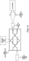
- FIG. 17 illustrates an example of a testing setup for testing a WMA interferometer 1700.
- the light source for testing the device is a tunable laser centered at 1550 run wavelength (Santec TSL-710).
- the power of the laser output is 1 mW.
- Light can be coupled into the waveguide with a tapered single mode fiber 1702 and the output can be imaged with a 40x objective 1704 onto InGaAs detectors 1706.
- Objective 1704 allows measurement of the two outputs of the MMI simultaneously by putting one detector at each output image location.
- a fiber polarization paddle can be used on the input fiber and a polarizer can be placed before the detector to eliminate the effects of stray TM modes.
- metal probes that are attached to electric cables can be used.
- the probes can be put in contact with the heaters on the chip and the electric cables can be connected to a voltage source 1708.
- the wavelength of the laser can be scanned and the output spectrum of the device can be recorded. For clarity reasons, only a connection for one heater is illustrated.
- FIG. 18 illustrates a plot showing the output light power as a function of input laser wavelength.
- the general trend of the spectrum shows the sinusoidal behavior we expect from a Mach-Zehnder interferometer.
- the ratio of the output powers is not as expected. This is most likely due to an undesired accumulation of phase, which can be compensated for by tuning heaters 2 and 3.
- the small fluctuation is due to the vibration of the input fiber during the scan. This can be largely improved by integrated photonics packaging techniques, such as fusing the fiber to the chip.
- FIG. 19 illustrates plots showing a modulated voltage signal (on the left) and an output light signal (on the right) measured using an radio-frequency (RF) spectrum analyzer.
- the modulation frequency components from the signal generator are 9.99 kHz, 10 kHz and 10.01 kHz. Since the response of the refractive index goes as the square of the applied voltage (i.e. power dissipated by the heater), the difference between the frequency components doubles in the measured output light. Accordingly, signal frequencies of 9.98 kHz and 10.02 kHz can be observed at the output. This demonstrates the ability of the device to measure changes to the phase difference between the interferometer arms by detecting the output light.
- FIG. 20 illustrates a simplified computer system 2000 according to some embodiments described herein.
- Computer system 2000 as illustrated in FIG. 20 may be incorporated into devices such as transmitter module 110, receiver module 120, or control/processing electronics 130 as described herein.
- FIG. 20 provides a schematic illustration of one example of computer system 2000 that can perform some or all of the steps of the methods provided by various embodiments. It should be noted that FIG. 20 is meant only to provide a generalized illustration of various components, any or all of which may be utilized as appropriate. FIG. 20 , therefore, broadly illustrates how individual system elements may be implemented in a relatively separated or relatively more integrated manner.
- Computer system 2000 is shown comprising hardware elements that can be electrically coupled via a bus 2005, or may otherwise be in communication, as appropriate.
- the hardware elements may include one or more processors 2010, including without limitation one or more general-purpose processors and/or one or more special-purpose processors such as digital signal processing chips, graphics acceleration processors, and/or the like; one or more input devices 2015, which can include without limitation a mouse, a keyboard, a camera, and/or the like; and one or more output devices 2020, which can include without limitation a display device, a printer, and/or the like.
- Computer system 2000 may further include and/or be in communication with one or more non-transitory storage devices 2025, which can comprise, without limitation, local and/or network accessible storage, and/or can include, without limitation, a disk drive, a drive array, an optical storage device, a solid-state storage device, such as a random access memory (“RAM”), and/or a read-only memory (“ROM”), which can be programmable, flash-updateable, and/or the like.
- RAM random access memory
- ROM read-only memory
- Such storage devices may be configured to implement any appropriate data stores, including without limitation, various file systems, database structures, and/or the like.
- Computer system 2000 might also include a communications subsystem 2019, which can include without limitation a modem, a network card (wireless or wired), an infrared communication device, a wireless communication device, and/or a chipset such as a Bluetooth TM device, an 802.11 device, a WiFi device, a WiMax device, cellular communication facilities, etc., and/or the like.
- the communications subsystem 2019 may include one or more input and/or output communication interfaces to permit data to be exchanged with a network such as the network described below to name one example, other computer systems, television, and/or any other devices described herein.
- a portable electronic device or similar device may communicate image and/or other information via the communications subsystem 2019.
- a portable electronic device e.g. the first electronic device
- computer system 2000 may be incorporated into computer system 2000, e.g., an electronic device as an input device 2015.
- computer system 2000 will further comprise a working memory 2035, which can include a RAM or ROM device, as described above.
- Computer system 2000 also can include software elements, shown as being currently located within the working memory 2035, including an operating system 2040, device drivers, executable libraries, and/or other code, such as one or more application programs 2045, which may comprise computer programs provided by various embodiments, and/or may be designed to implement methods, and/or configure systems, provided by other embodiments, as described herein.
- application programs 2045 may comprise computer programs provided by various embodiments, and/or may be designed to implement methods, and/or configure systems, provided by other embodiments, as described herein.
- code and/or instructions can be used to configure and/or adapt a general purpose computer or other device to perform one or more operations in accordance with the described methods.
- a set of these instructions and/or code may be stored on a non-transitory computer-readable storage medium, such as the storage device(s) 2025 described above.
- the storage medium might be incorporated within a computer system, such as computer system 2000.
- the storage medium might be separate from a computer system e.g., a removable medium, such as a compact disc, and/or provided in an installation package, such that the storage medium can be used to program, configure, and/or adapt a general purpose computer with the instructions/code stored thereon.
- These instructions might take the form of executable code, which is executable by computer system 2000 and/or might take the form of source and/or installable code, which, upon compilation and/or installation on computer system 2000 e.g., using any of a variety of generally available compilers, installation programs, compression/decompression utilities, etc., then takes the form of executable code.
- some embodiments may employ a computer system such as computer system 2000 to perform methods in accordance with various embodiments of the technology. According to a set of embodiments, some or all of the procedures of such methods are performed by computer system 2000 in response to processor 2010 executing one or more sequences of one or more instructions, which might be incorporated into the operating system 2040 and/or other code, such as an application program 2045, contained in the working memory 2035. Such instructions may be read into the working memory 2035 from another computer-readable medium, such as one or more of the storage device(s) 2025. Merely by way of example, execution of the sequences of instructions contained in the working memory 2035 might cause the processor(s) 2010 to perform one or more procedures of the methods described herein. Additionally or alternatively, portions of the methods described herein may be executed through specialized hardware.
- machine-readable medium and “computer-readable medium,” as used herein, refer to any medium that participates in providing data that causes a machine to operate in a specific fashion.
- various computer-readable media might be involved in providing instructions/code to processor(s) 2010 for execution and/or might be used to store and/or carry such instructions/code.
- a computer-readable medium is a physical and/or tangible storage medium.
- Such a medium may take the form of a non-volatile media or volatile media.
- Non-volatile media include, for example, optical and/or magnetic disks, such as the storage device(s) 2025.
- Volatile media include, without limitation, dynamic memory, such as the working memory 2035.
- Common forms of physical and/or tangible computer-readable media include, for example, a floppy disk, a flexible disk, hard disk, magnetic tape, or any other magnetic medium, a CD-ROM, any other optical medium, punchcards, papertape, any other physical medium with patterns of holes, a RAM, a PROM, EPROM, a FLASH-EPROM, any other memory chip or cartridge, or any other medium from which a computer can read instructions and/or code.
- Various forms of computer-readable media may be involved in carrying one or more sequences of one or more instructions to the processor(s) 20 10 for execution.
- the instructions may initially be carried on a magnetic disk and/or optical disc of a remote computer.
- a remote computer might load the instructions into its dynamic memory and send the instructions as signals over a transmission medium to be received and/or executed by computer system 2000.
- the communications subsystem 2019 and/or components thereof generally will receive signals, and the bus 2005 then might carry the signals and/or the data, instructions, etc. carried by the signals to the working memory 2035, from which the processor(s) 2010 retrieves and executes the instructions.
- the instructions received by the working memory 2035 may optionally be stored on a non-transitory storage device 2025 either before or after execution by the processor(s) 2010.
- configurations may be described as a process which is depicted as a schematic flowchart or block diagram. Although each may describe the operations as a sequential process, many of the operations can be performed in parallel or concurrently. In addition, the order of the operations may be rearranged. A process may have additional steps not included in the figure.
- examples of the methods may be implemented by hardware, software, firmware, middleware, microcode, hardware description languages, or any combination thereof. When implemented in software, firmware, middleware, or microcode, the program code or code segments to perform the necessary tasks may be stored in a non-transitory computer-readable medium such as a storage medium. Processors may perform the described tasks.
Landscapes
- Physics & Mathematics (AREA)
- Engineering & Computer Science (AREA)
- General Physics & Mathematics (AREA)
- Computer Networks & Wireless Communication (AREA)
- Radar, Positioning & Navigation (AREA)
- Remote Sensing (AREA)
- Electromagnetism (AREA)
- Instruments For Measurement Of Length By Optical Means (AREA)
- Measurement Of Mechanical Vibrations Or Ultrasonic Waves (AREA)
- Optical Modulation, Optical Deflection, Nonlinear Optics, Optical Demodulation, Optical Logic Elements (AREA)
- Optical Radar Systems And Details Thereof (AREA)
- Photometry And Measurement Of Optical Pulse Characteristics (AREA)
Description
- This application relates to a method and apparatus for performing remote sensing of vibrations and claims priority to
US Provisional Application No. 62/748,990 filed on October 22, 2018 - Laser vibrometers have been used to make non-contact vibration measurements of a surface. In some instances, a test beam is transmitted to the surface of interest and a reflected laser beam is received and analyzed to extract a Doppler shift due to the motion of the surface of interest. A typical laser vibrometer requires access to a reference beam that is identical in frequency to the test beam. Prior to reaching the surface of interest, the test beam passes through a Bragg cell, which adds a frequency shift. The reflected beam has a frequency containing the frequency of the test beam, the frequency shift, and the Doppler shift. The reflected beam and the reference beam are fed into a photodetector and the Doppler shift is thereafter estimated by investigating the beat frequency between the two beams.
- Despite the usefulness of conventional vibrometers in many applications, the requirement of access to a local copy of the test beam (i.e., a reference beam) makes the conventional approach ill suited for remote sensing. Accordingly, new systems, methods, and other techniques are needed.
DocumentUS 2005/0185191 A1 discloses an optical system providing information about tangential vibration components of a surface at remote location. The optical system includes a light source that emits two beams directed at the interrogated surface. A detector system detects a third beam formed by the reflected beams, and provides information on a phase change. - The present invention relates to a method of performing remote sensing as defined in
claim 1 and to an apparatus as defined inclaim 8. - Further details of the invention are set forth in the dependent claims.
- Numerous benefits are achieved by way of the present invention. For example, with conventional laser Doppler vibrometers, a local oscillator or a local copy of the interrogation laser signal is required so as to detect the frequency differences between the interrogation laser signal and the reflected laser signal caused by the surface of interest. Additionally, embodiments of the present invention are not limited by the coherence length of the laser source, thereby extending the usable range of the device. Furthermore, embodiments of the present invention include a chip scale inteferometer that can be fabricated significantly more compactly and inexpensively compared to conventional interferometers. The chip scale interferometer is not limited to vibrometry applications, but can be used in a wide variety of frequency measurement systems. Examples of possible applications beyond vibrometry include a number of laboratory-scale measurement setups, medical imaging, telecommunication networks, navigation systems, radar systems, and the like. Other benefits of the present invention will be readily apparent to those skilled in the art.
- A further understanding of the nature and advantages of various embodiments may be realized by reference to the following figures. In the appended figures, similar components or features may have the same reference label. Further, various components of the same type may be distinguished by following the reference label by a dash and a second label that distinguishes among the similar components. If only the first reference label is used in the specification, the description is applicable to any one of the similar components having the same first reference label irrespective of the second reference label.
-
FIG. 1 illustrates a block diagram of a vibrometer. -
FIG. 2 illustrates an example of a vibrometer comprising a plurality of weak measurement amplification (WMA) interferometers. -
FIG. 3 illustrates an example of a WMA interferometer. -
FIG. 4 illustrates an example of the signal intensity of the TM0 mode of a reflected signal within a WMA interferometer. -
FIG. 5 illustrates an example of the signal intensity of the TM1 mode of a reflected signal within a WMA interferometer. -
FIG. 6 illustrates an example of the power transfer between waveguides of the TM0 mode. -
FIG. 7 illustrates an example of the power transfer between waveguides of the TM1 mode. -
FIG. 8 illustrates an example of detection of the intensity difference S by a split detector. -
FIG. 9 illustrates spatial and temporal resolution of intensity differences S and Doppler frequencies fd corresponding to the embodiment shown inFIG. 2 . -
FIGS. 10A-10B illustrate a method of performing remote sensing using WMA. -
FIG. 11 illustrates an example layout of a WMA interferometer. -
FIG. 12 illustrates an example layout of a mode converter. -
FIG. 13 illustrates a plot showing the mode effective index change as a function of waveguide width. -
FIG. 14 illustrates an example layout of a multimode interferometer. -
FIG. 15 illustrates a plot showing a simulated output of a multimode interference waveguide as a function of the ratio of TE0 and TE1 mode. -
FIG. 16 illustrates an example layout of a WMA interferometer with heaters. -
FIG. 17 illustrates an example of a testing setup for testing a WMA interferometer. -
FIG. 18 illustrates a plot showing the output light power as a function of input laser wavelength. -
FIG. 19 illustrates plots showing a modulated voltage signal (on the left) and an output light signal (on the right) measured using an radio-frequency (RF) spectrum analyzer. -
FIG. 20 illustrates a simplified computer system. - Weak value amplification (WVA) and inverse weak value amplification (IWVA) using free space optics have enabled ultrasensitive measurements in applications such as beam deflection, frequency shifts, and phase shifts. The weak value technique allows the amplification of small signals by introducing a weak perturbation to the system and performing a post-selection to the data.
- Bringing weak value techniques to the field of integrated photonics improves its applications. For example, it largely reduces the size of the measuring system to millimeter scale. Also, an integrated photonic device is inherently stable; therefore it is less susceptible to environmental factors such as vibrations. With an on-chip weak value amplification device, precision measurements can be carried out in a small volume with reliable performance.
- In some instances, IWVA can be demonstrated using free space optics and a misaligned Sagnac interferometer. One goal may be to measure the relative phase shift φ between the two paths of the interferometer. The misalignment introduces a phase front tilt k to one path of the interferometer and -k to the other.


- To bring free space IWVA to the integrated photonics regime, the above expressions are expanded into Hermite-Gaussian (HG) modes. The beams are composed mainly of the HG1 mode with a small contribution of the HG0 mode. Contribution of the higher modes is negligible. Therefore, the phase front tilt can be considered as coupling the initial HG0 mode partially into the HG1 mode.


- Eigenmodes of a waveguide are similar to Hermite-Gaussian modes. The theory described above can be applied to waveguide eigenmodes TE0 and TE1. Assuming that a TE0 mode is sent into an upper waveguide of the device. Its power is split in half and the fields become,


- Similar to free space case, part of the TE0 mode is coupled to the TE1 mode with opposite phases in the two paths. a is the percentage of the TE0 mode coupled to the TE1 mode, which is a small number.


- After the two paths interfere at the second 50/50 splitter, the dark port becomes,


- Embodiments of the invention are related to methods and systems for performing long range vibrometry using weak measurement amplification (WMA). Specifically, embodiments relate to a chip scale integrated optics WMA sensor for detecting vibration signals of remote vibrating targets. According to some embodiments, an interrogation laser is transmitted toward a remote vibrating target and return vibration signals (micro-Doppler) are imaged with a chip scale WMA receiver sensor to produce target vibration profiles. This approach enables ultra-sensitive vibrometry without the need for long coherence length lasers and significantly reduces technical noise. The approach also enables longer range vibrometry missions than the current state of the art of commercial remote vibrometers. An integrated photonics implementation at the chip scale provides for significant reduction in platform vibration sensitivity of the vibrometer platform, allowing the WMA sensor to measure the target effects versus the platform effects. The implementation of weak value and inverse weak value based detection with several different interferometer geometries using guided waves in a monolithic geometry enables the implementation of the WVA effect in an ultrasmall package (compared to conventional interferometer packages). This advances WMA to real world applications by reducing effects related to the vibrometer platform.
- In some embodiments, a tapered fiber coupler couples light from a specific target location within the receiver's field of view onto an individual chip scale silicon waveguide, which is designed to form an interferometer by creating two beam splitters in the waveguide's propagation path. The signal injected into the waveguide from the remote vibrating target contains both the initial laser frequency (i.e., the interrogation frequency) and the Doppler and Micro-Doppler signals superimposed on top of the initial laser frequency (e.g., a THz laser frequency). The waveguide is designed with a given refractive index difference to create two modes of propagation, for example, by spatially varying the index of refraction across the transverse profile of the waveguide. The two beam splitters cause constructive interference of a higher, information-containing mode and destructive interference of the lowest mode.
-
FIG. 1 illustrates a block diagram of avibrometer 100, according to some embodiments of the present invention.Vibrometer 100 includes atransmitter module 110 configured to transmit aninterrogation signal 106 to a remote vibratingtarget 108 and areceiver module 120 configured to receive a reflectedsignal 112 generated byinterrogation signal 106 being reflected off remote vibratingtarget 108.Transmitter module 110 may include aninterrogation laser 102 for modulatinginterrogation signal 106 at an interrogation frequency fo , typically in the THz frequency range. Optionally, anafocal expander 104 can be used to expandinterrogation signal 106 prior to transmission thereof to reduce beam divergence.Receiver module 120 may include areceiver telescope 116 for collecting reflectedsignal 1 12 from a specific target location within the field of view ofvibrometer 100 and for imaging reflectedsignal 112 onto aWMA interferometer 150. As described herein,WMA interferometer 150 processes reflectedsignal 112 in a way that allows extraction of a Doppler frequency fd introduced onto reflectedsignal 112 by remote vibratingtarget 108. - In some embodiments,
vibrometer 100 includes control/processing electronics 130 that is communicatively coupled to each oftransmitter module 110 andreceiver module 120. For example, control/processing electronics 130 may send control signals to and receive information signals from each oftransmitter module 110 andreceiver module 120. According to at least one embodiment, control/processing electronics 130 may send a set of control signals totransmitter module 110 so as to turn oninterrogation laser 102, set the interrogation frequency fo , and causeinterrogation laser 102 to point at remote vibratingtarget 108. The set of control signals may implement more sophisticated control algorithms in which, as an example, the interrogation frequency fo may be driven over a range of frequencies while remote vibratingtarget 108 is spatially scanned by directinginterrogation laser 102 across the field of view. Control/processing electronics 130 may generate target vibration profiles such asDoppler images 132 based on the output ofWMA interferometer 150. -
FIG. 2 illustrates an example ofvibrometer 100 comprising a plurality ofWMA interferometers 150, according to some embodiments of the present invention. In some embodiments,receiver telescope 116 may include anobjective lens 114 configured to image reflectedsignal 112 onto aparticular WMA interferometer 150 of a plurality ofWMA interferometers 150 based on the angle of arrival of reflectedsignal 112. In some embodiments, each of the plurality ofWMA interferometers 150 corresponds to a pixel ofDoppler image 132. Outputs of the plurality ofWMA interferometers 150 may be fed into a digital readout integratedcircuit 118 that processes the outputs and/or serializes the outputs into a data stream that is provided to control/processing electronics 130. In some embodiments, digital readout integratedcircuit 118 behaves as a multiplexer that forwards one or more of the outputs of the plurality ofWMA interferometers 150 as requested by control/processing electronics 130. -
FIG. 3 illustrates an example ofWMA interferometer 150, according to some embodiments of the present invention.WMA interferometer 150 includes a first waveguide 312-1 and a second waveguide 312-2 for propagating reflectedsignal 112.WMA interferometer 150 may include one or two input ports, such as a first port 306-1 coupled to first waveguide 312-1 and a second port 306-2 coupled to second waveguide 312-2. A taperedfiber coupler 302 may be coupled to first port 306-1 and may be configured to receive reflectedsignal 112. In the illustrated embodiment, second port 306-2 is coupled to vacuum or to an ambient atmosphere. - Portions of first waveguide 312-1 may be positioned in close proximity (e.g., within a threshold distance) to portions of second waveguide 312-2 to implement first beam splitter 310-1 and second beam splitter 310-2. First beam splitter 310-1 may be configured to split reflected
signal 112 into a first portion of reflected signal 112-1 and a second portion of reflected signal 112-2, where first portion 112-1 corresponds to the portion of reflectedsignal 112 that propagates down first waveguide 312-1 after being split by first beam splitter 310-1 and second portion 112-2 corresponds to the portion of reflectedsignal 112 that propagates down second waveguide 312-2 after being split by first beam splitter 310-1. Second beam splitter 310-2 splits first portion of reflected signal 112-1 and second portion of reflected signal 112-2 into third portion of reflected signal 112-3 and fourth portion of reflected signal 112-4, where third portion 112-3 corresponds to the portion(s) of first portion 112-1 and second portion 112-2 that propagates down first waveguide 312-1 after being split by second beam splitter 310-2 and fourth portion 112-4 corresponds to the portion(s) of first portion 112-1 and second portion 112-2 that propagates down second waveguide 312-2 after being split by second beam splitter 310-2. - In the illustrated embodiment,
WMA interferometer 150 includes adelay element 330, such as a Bragg grating, positioned along second waveguide 312-2 between beam splitters 310. In some embodiments,delay element 330 is positioned along first waveguide 312-1 between beam splitters 310. In some embodiments, two delay elements (e.g., two Bragg gratings) positioned along both of waveguides 312 are utilized.Delay element 330 may be configured to delay the phase of second portion of reflected signal 112-2 such that second portion 112-2 acquires a relative phase ϕ compared to first portion 112-1. This may be accomplished by fabricatingdelay element 330 to have a periodic variation in the index of refraction. - In some embodiments,
WMA interferometer 150 includes a first spatial phase shifter 318-1 positioned along first waveguide 312-1 configured to spatially phase shift first portion of reflected signal 112-1 and a second spatial phase shifter 318-2 positioned along second waveguide 312-2 configured to spatially phase shift second portion of reflected signal 112-2 such that the modes TM0 and TM1 acquire opposite tilted phase fronts resulting in a relative phase shift between the two modes. In some embodiments, an extra spatial phase shift is created of the form e ±iKx , which is equivalent to bringing out the next mode. In some embodiments, only a single spatial phase shifter is used. One or both of spatial phase shifters 318 may be positioned at different positions withinWMA interferometer 150 than that shown in the illustrated embodiment, such as beforedelay element 330 and/or before beam splitter 310-1 (in reference to the direction of propagation). In some embodiments, one or both of spatial phase shifters 318 may include a mode exciter, such as a prism, fabricated within one or both of waveguides 312 configured to excite a superposition of odd order modes inreflected signal 112. The mode exciter may include a gradient in the index of refraction across the transverse profile of the waveguide causing some of the electric field amplitude to be transferred to the first excited mode. In some embodiments, spatial phase shifters 318 are implemented by widening waveguides 312 at a particular widening point alongwaveguides 3 12 such that only a single mode is supported prior to the widening point and a second mode is supported after the widening point. - In some embodiments,
WMA interferometer 150 includes asplit detector 322 coupled to first waveguide 312-1.Split detector 322 is configured to receive third portion of reflected signal 112-3 and detect an intensity difference S between a first lobe and a second lobe of third portion 112-3. Due to the TM0 and TM1 modes acquiring opposite tilted phase fronts during propagation inWMA interferometer 150, second beam splitter 310-2 causes destructive interference of the TM0 mode and enhances the relative contribution of the TM1 mode within third portion 112-3. Accordingly, a significant portion of the detectable power in third portion 112-3 resides in the information-containing TM1 mode. -
FIG. 4 illustrates an example of the signal intensity of the TM0 mode of reflectedsignal 112 withinWMA interferometer 150, according to some embodiments of the present invention. Prior to reaching first beam splitter 310-1, power in the TM0 mode is concentrated in first waveguide 312-1. When reflectedsignal 112 propagates through first beam splitter 310-1, power in the TM0 mode is 50/50 split between waveguides 312. When reflectedsignal 1 12 propagates through second beam splitter 310-2, power in the TM0 mode shifts to second waveguide 312-2. -
FIG. 5 illustrates an example of the signal intensity of the TM1 mode of reflectedsignal 1 12 withinWMA interferometer 150, according to some embodiments of the present invention. Prior to reaching first beam splitter 310-1, power in the TM1 mode is concentrated in first waveguide 312-1. When reflectedsignal 1 12 propagates through first beam splitter 310-1, power in the TM1 mode remains in first waveguide 312-1. When reflectedsignal 112 propagates through second beam splitter 310-2, power in the TM1 mode remains in first waveguide 312-1. -
FIG. 6 illustrates an example of the power transfer between waveguides of the TM0 mode as the beam propagates along the Z-axis, according to some embodiments of the present invention. The Y-axis coming out of the page corresponds to signal intensity level, which is shown on the right. In the illustrated embodiment, the upper and lower waveguides are positioned sufficiently close over a particular propagation distance such that coupling by evanescent waves in the cladding causes power in the TM0 mode to split 50/50 between the waveguides. -
FIG. 7 illustrates an example of the power transfer between waveguides of the TM1 mode as the beam propagates along the Z-axis, according to some embodiments of the present invention. The Y-axis coming out of the page corresponds to signal intensity level, which is shown on the right. In the illustrated embodiment, the upper and lower waveguides are positioned sufficiently close over a particular propagation distance such that coupling by evanescent waves in the cladding causes power in the TM1 mode to remain in the upper waveguide. -
FIG. 8 illustrates an example of detection of the intensity difference S bysplit detector 322, according to some embodiments of the present invention. In some embodiments, the intensity difference S may be calculated as S = IR-IL where IR is the intensity of the right half of the waveguide and IL is the intensity of the left half of the waveguide. In some embodiments, the intensity difference S may be calculated as S = (IR -IL )/(IR +IL ).Split detector 322 may include aleft area 326 and aright area 328 for detecting intensities IL and IR , respectively. In the illustrated embodiment, an intensity difference of S1 = 0 detected at time T1 is shown inprofile 802 and an intensity difference of S2 > 0 detected at time T2 is shown inprofile 804. - In some embodiments, the intensity difference S may be used to calculate the Doppler frequency fd as follows. If the system is calibrated to a fiducial frequency ω (where the balanced signal is 0), then a slight change of frequency from remote vibrating
target 108 will have the following chain of dependencies. The relative phase shift between the arms of the interferometer (i.e., first and second waveguides 312) is controlled by the combination n(ω)ω ΔL/c, where n is the frequency-dependent index of refraction, ΔL is the path length difference, and c the speed of light. Therefore, a change of frequency δω will result in a change of relative phase of δφ = δω (∂ω/∂φ)-1 ≈ τg δω, where τg is the "group delay", the amount of temporal delay a pulse of light will suffer going through the dispersive medium, which is proportional to the frequency derivative of the index of refraction. The normalized signal read out by the split detector S = (IR -IL )/(IR +IL ) is related to the relative phase φ by S = cm φ/(κd), where κ is the tilt of the phase front, d is the width of the waveguide (spatial spread of the mode), and cm is a constant related to the mode function. Thus, for small phase shifts, there is a linear relation between phase and detected signal. Combining the above observations, a shift in frequency δω is related to a shifted signal reading δS as follows: δS = ((cm τg)/κd)δω. Consequently, the larger the group delay, the more signal is obtained for the same amount of Doppler shift. Similarly, the 1/κ is the weak value amplification effect. -
FIG. 9 illustrates spatial and temporal resolution of intensity differences S and Doppler frequencies fd corresponding to the embodiment shown inFIG. 2 . Each of intensity differences S is characterized by two indexes: the particular WMA interferometer (numbered 1 through 16) that detected the intensity difference and the time (numbered 1, 2, ... , N) at which the intensity difference was detected. As illustrated, intensity differences S detected across time and spatial values are converted into Doppler frequencies fd over the same time and spatial values. - Referring once again to
FIG. 9 , thespatial map 910 of intensity difference S has been converted into aspatial map 912 of Doppler frequencies fd at a first time (T 1). Spatial maps of the intensity differences (spatial maps 920 and 930) are illustrated for a second time (T 2) and an Nth time, respectively. Additionally, spatial maps of Doppler frequencies fd (spatial maps 922 and 932) are illustrated for the second time (T 2) and the Nth time, respectively. Accordingly, embodiments of the present invention enable spatial maps of the vibrometry data associated with remote vibratingtarget 108 to be measured and subsequently utilized as appropriate to the particular application. -
FIGS. 10A-10B illustrate amethod 1000 of performing remote sensing using WMA, according to some embodiments of the present invention. One or more steps ofmethod 1000 may be performed in a different order than the illustrated embodiment, and one or more steps ofmethod 1000 may be omitted during performance ofmethod 1000. - At
step 1002,interrogation laser 102 modulatesinterrogation signal 106 at an interrogation frequency fo. In some embodiments, the interrogation frequency fo is selected to be near the band gap ofdelay element 330. In various embodiments, the interrogation frequency fo may be any one of 400 THz, 450 THz, 500 THz, 550 THz, 600 THz, 650 THz, 700 THz, among other possibilities. - At
step 1004,afocal expander 104 expandsinterrogation signal 102. In some embodiments,afocal expander 104 expandsinterrogation signal 102 to reduce beam divergence so as to maximize energy on remote vibratingtarget 108. In some embodiments,afocal expander 104 includesobjective lens 114. - At
step 1006,transmitter module 110 transmitsinterrogation signal 106 to remote vibratingtarget 108. In some embodiments,step 1006 may includeinterrogation laser 102 transmittinginterrogation signal 106 throughafocal expander 104 toward remote vibratingtarget 108. Wheninterrogation signal 106 is reflected by remote vibratingtarget 108, a target-own platform Doppler shift is introduced by remote vibratingtarget 108 and a target micro-Doppler shift is induced by localized surface vibrations on remote vibratingtarget 108. - At
step 1008,receiver telescope 116 collects reflectedsignal 112 from a specific target location within the field of view ofvibrometer 100 and images reflectedsignal 112 onto taperedfiber coupler 302. In some embodiments, thereceiver telescope 116 may image reflectedsignal 112 onto a particulartapered fiber coupler 302 of a plurality of tapered fiber couplers based on the angle of arrival of reflectedsignal 112. - At
step 1010, first port 306-1 receives reflectedsignal 112. In some embodiments,step 1010 includes first port 306-1 receiving reflectedsignal 112 from taperedfiber coupler 302. Concurrently with or subsequent to step 1010, first waveguide 312-1 may receive reflectedsignal 112 via first port 306-1 and reflectedsignal 112 may propagate down first waveguide 312-1. - At
step 1012, first beam splitter 310-1 splits reflectedsignal 112 into first portion of reflected signal 112-1 and second portion of reflected signal 112-2, where first portion 112-1 corresponds to the portion of reflectedsignal 112 that propagates down first waveguide 312-1 after being split by first beam splitter 310-1 and second portion 112-2 corresponds to the portion of reflectedsignal 112 that propagates down second waveguide 312-2 after being split by first beam splitter 310-1. In some embodiments, first beam splitter 310-1 is formed by positioning first and second waveguides 312 within a threshold distance from each other such that reflectedsignal 112 is coupled into first and second waveguides 312 via evanescent wave coupling. By bringing first and second waveguides 312 sufficiently close, coupling by evanescent waves in the cladding causes power to shift between each waveguide as a function of propagation distance. Such an effect can be utilized to create a reliable analog for a free space 50/50 beam splitter. - At
step 1014,delay element 330 delays the phase of second portion of reflected signal 112-2 such that second portion 112-2 acquires a relative phase ϕ compared to first portion 112-1. In some embodiments,delay element 330 includes a Bragg grating. In some embodiments,delay element 330 may be fabricated to have a periodic variation in the index of refraction. Traveling waves withindelay element 330 have solutions of the form β = β B ±(δ2-κ2)1/2 which yields a photonic bandgap where the group velocity goes to 0 as Vg = ∂β/βω, implying competition between high dispersion and high transmission. In some embodiments, a double Bragg grating may be employed having two band gaps with couplings κ1 and κ2 providing two spatial wavelengths. Such embodiments comprising two band gaps create a frequency window of high transmission, high dispersion, and low group velocity. - Although
delay element 330 is described herein as being positioned along second waveguide 312-2, in some embodiments delayelement 330 may be positioned along first waveguide 312-1 so as to delay the phase of first portion of reflected signal 112-2. In some embodiments, a first delay element may be positioned along first waveguide 312-1 so as to delay the phase of first portion 112-1 and a second delay element may be positioned along second waveguide 312-2 so as to delay the phase of second portion 112-2. In some embodiments,delay element 330 acts like a Rubidium cell that may be implemented in free space embodiments, causing a relative phase ϕ between the two arms. - At
step 1016, first spatial phase shifter 318-1 positioned along first waveguide 312-1 spatially phase shifts first portion of reflectedsignal 1 12-1 and second spatial phase shifter 318-2 positioned along second waveguide 312-2 spatially phase shifts second portion of reflected signal 112-2 such that the modes TM0 and TM1 acquire opposite tilted phase fronts resulting in a relative phase shift between the two modes. In some embodiments, only a single spatial phase shifter is used. In some embodiments, one or both of first-spatial phase shifter 318-1 and second-spatial phase shifter 318-2 are configured to excite a superposition of odd order modes in first portion 112-1 and second portion 112-2, respectively. This may be accomplished by fabricating a prism within one or both of first waveguide 312-1 and second waveguide 312-2. For example, the prism may include a gradient in the index of refraction across the transverse profile of first waveguide 312-1 and/or second waveguide 312-2 causing some of the electric field amplitude to be transferred to the first excited mode. In some embodiments, the prism may excite a superposition of odd order modes from an initial zeroth-order mode input. The prism may thereby cause reflectedsignal 112 to propagate in accordance with two modes of propagation. - At
step 1018, second beam splitter 310-2 splits first portion of reflected signal 112-1 and second portion of reflected signal 112-2 into third portion of reflected signal 112-3 and fourth portion of reflected signal 112-4, where third portion 112-3 corresponds to the portion(s) of first portion 112-1 and second portion 112-2 that propagates down first waveguide 312-1 after being split by second beam splitter 310-2 and fourth portion 112-4 corresponds to the portion(s) of first portion 112-1 and second portion 112-2 that propagates down second waveguide 312-2 after being split by second beam splitter 310-2. In some embodiments, second beam splitter 310-2 is formed by positioning first and second waveguides 312 within a threshold distance from each other such that first portion 112-1 and second portion 112-2 are coupled into first and second waveguides 312 via evanescent wave coupling. Due to the TM0 and TM1 modes acquiring opposite tilted phase fronts instep 1018, second beam splitter 310-2 causes destructive interference of the TM0 mode and enhances the relative contribution of the TM1 mode within third portion 112-3. - At
step 1020, splitdetector 322 receives third portion of reflected signal 112-3 and detects an intensity difference S between a first lobe and a second lobe of third portion 112-3. WhenWMA interferometer 150 is tuned to operate in the inverse weak value region, a double lobe pattern is produced onsplit detector 322. In some embodiments, splitdetector 322 comprises a two element detector or two separate detectors having a right-side and a left-side. In some embodiments, splitdetector 322 identifies two relative maximum intensity values and determines a difference between them. In some embodiments, splitdetector 322 determines two intensity values at two predetermined spatial positions (e.g., x = ±1·10-6 m). In some embodiments, a Y-branch may be used to spatially split the profile of third portion 112-3 to measure and detect the intensity difference S. - At
step 1022, a processor ofvibrometer 100 calculates the Doppler frequency fd based on the intensity difference S. WhenWMA interferometer 150 is properly tuned, the intensity difference S will shift due to changes in frequency (Doppler change). As such, the rate of change of the intensity difference S with respect to the rate of change in frequency can be calculated.Step 1022 may be performed by a processor withinreceiver module 120 or control/processing electronics 130, among other possibilities. -
FIG. 11 illustrates an example layout of aWMA interferometer 1100, according to some embodiments of the present invention.WMA interferometer 1100 includes a first and second directional couplers (DC1 and DC2), multi-mode interferometers (MMI), and outputs (O1, O2, O3, and O4). In some embodiments, for the design of the device, silicon nitride can be used as the guiding material, silicon dioxide can be used as the cladding material, and the testing wavelength can be 1550 nm. These materials and wavelength have good compatibility with existing fabrication and testing techniques. A thickness of 300 nm for silicon nitride is chosen for balance of confinement and ease of coupling. - A free space Mach-Zander interferometer can be achieved by two beam-splitters. On a photonic chip, the analog of a beam-splitter is a directional coupler. When two waveguides are close and the modes in them are phase matched, light in one of the waveguides will couple to the other. The coupling ratio depends on the separation between the two waveguides and the length of the coupling region. This structure is called a directional coupler.
-
FIG. 12 illustrates an example layout of amode converter 1200, according to some embodiments of the present invention.Mode converter 1 200 can be used to introduce a phase front tilt by coupling part of the fundamental mode (TE0) to the second order mode (TE1). The input waveguide W1, which may be the bottom waveguide, may be a single mode waveguide that only supports the TE0 mode. At the first directional coupler, a small portion of the input TE0 mode is coupled to the TE0 mode of an identical waveguide W2, which may be the top waveguide. W1 then enters a tapering region where the width of W1 gradually increases until it becomes a multimode waveguide that supports both the TE0 and TE1 modes. Because the change in width is slow, light in the TE0 mode will tend to stay confined in the TE0 mode instead of coupling to higher order modes and dissipating. - The TE1 mode supported by W1 can be designed to be phase matched with TE0 in W2. Therefore, at the second directional coupler, TE0 in W2 will couple to TE1 in W1. Since TE0 in W1 is not phase matched with any mode in W2, it will stay in W1. As a result, W1 will contain mostly the TE0 mode with a small amount of the TE1 mode at the end of this structure. The ratio between the two modes depends on the coupling ratio of the first directional coupler. And the phase difference between the two modes depends on the optical path difference of W1 and W2 between the two couplers.
-
FIG. 13 illustrates a plot showing the mode effective index change as a function of waveguide width, according to some embodiments of the present invention.FIG. 13 demonstrates that the widths of the waveguide can be designed to match the TE0 and TE1 modes with an effective index of 1.6, which corresponds to a width of 1.2 µm for W2 and 2.75 µm for W1. -
FIG. 14 illustrates an example layout of amultimode interferometer 1400, according to some embodiments of the present invention. In some embodiments, the mean location shift can be measured by measuring the ratio of TE0 and TE1 mode in the dark port. Therefore, a multimode interference waveguide can be used, which reacts differently to the TE0 and TE1 modes. An multimode interference waveguide is a segment of waveguide that supports many modes followed by two single mode waveguides. In the multimode interference region, light is coupled to a number of modes, which have different propagation velocity. Therefore, their interference pattern changes as they propagate, thus changing the output power of the two single mode waveguides. -
FIG. 15 illustrates a plot showing a simulated output of a multimode interference waveguide as a function of the ratio of TE0 and TE1 mode. As illustrated, simulations of the multimode interference waveguide using the eigenmode multimode interference expansion method (FIMMPROP, Photon Design) show that, while the output ratio of the TE0 mode or the TE1 mode is 50/50, the addition of the two modes gives a different result. As the percentage of the TE0 mode increases, one of the outputs decreases. This allows the ratio of the TE0 and TE1 modes to be determined with the output light signal. -
FIG. 16 illustrates an example layout of aWMA interferometer 1600 with heaters, according to some embodiments of the present invention. For the purpose of testing the device, a source of phase φ may be required. A common method to add phase tunability to waveguides is to use micro-heaters. By depositing metal wires on top of the waveguide cladding and applying voltage on them, they can generate heat and increase the temperature of the waveguide underneath. The temperature change will induce a refractive index change of the waveguide material, introducing a phase difference compared to the unheated waveguide. A first heater (H1) may be placed after the first directional coupler to introduce a deliberate phase difference for measurement. - Heaters are also useful for the undesired phase accumulation throughout the device due to fabrication errors. In theory, when phase φ = 0, the TE0 and TE1 modes need to be in phase before they interfere. Other sources of phase accumulation will reduce the sensitivity of the measurement. To compensate for these undesired sources of phase, two other heaters may be placed on each path of the device to tune the two modes in phase before applying the target phase φ. Heater 2 (H2) may control the relative phase of the TE1 mode to the TE0 mode. Heater 3 (H3) may compensate for the phase difference between the TE0 and TE1 due to their different propagation velocities.
- In some implementations,
WMA interferometer 1600 can be fabricated from a 4-inch silicon wafer with 4 µm of thermally grown silicon dioxide. A layer of 289 nm of silicon nitride can be deposited with low pressure chemical vapor deposition (LPCVD). The waveguides can then be patterned with e-beam lithography and the silicon nitride can be etched with inductively coupled plasma reactive ion etching (ICP-RIE). The waveguides can be cladded with 2.6 µm of silicon dioxide deposited via plasma enhanced chemical vapor deposition (PECVD). - To place heaters on top of the waveguides, a "lift-off" method can be employed as follows. First, a layer of photoresist is spun on top of the silicon dioxide and the shape of the heaters can be patterned with DUV photolithography (ASML 300C DUV Stepper - 248nm). Then, deposit 10nm of chrome is deposited for adhesion to the silicon dioxide and 100 nm of platinum as the heaters. Next, the wafer is immersed in acetone, which dissolves the photoresist and thus removes the extra metal. The metal left on the surface of the cladding forms the heaters over the waveguides.
-
FIG. 17 illustrates an example of a testing setup for testing aWMA interferometer 1700. In some implementations, the light source for testing the device is a tunable laser centered at 1550 run wavelength (Santec TSL-710). The power of the laser output is 1 mW. Light can be coupled into the waveguide with a taperedsingle mode fiber 1702 and the output can be imaged with a 40x objective 1704 ontoInGaAs detectors 1706.Objective 1704 allows measurement of the two outputs of the MMI simultaneously by putting one detector at each output image location. A fiber polarization paddle can be used on the input fiber and a polarizer can be placed before the detector to eliminate the effects of stray TM modes. - To apply voltage to the heaters, metal probes that are attached to electric cables can be used. The probes can be put in contact with the heaters on the chip and the electric cables can be connected to a
voltage source 1708. Without applying any voltage to the heaters, the wavelength of the laser can be scanned and the output spectrum of the device can be recorded. For clarity reasons, only a connection for one heater is illustrated. -
FIG. 18 illustrates a plot showing the output light power as a function of input laser wavelength. The general trend of the spectrum shows the sinusoidal behavior we expect from a Mach-Zehnder interferometer. However, the ratio of the output powers is not as expected. This is most likely due to an undesired accumulation of phase, which can be compensated for by tuningheaters - Because of the fiber fluctuation, it is difficult to determine the cause of light signal change when a constant phase signal is applied. Therefore, a modulated phase signal can be sent. When
heater 1 is tuned with a sine wave voltage signal, a light signal with a corresponding frequency can be observed at the output. -
FIG. 19 illustrates plots showing a modulated voltage signal (on the left) and an output light signal (on the right) measured using an radio-frequency (RF) spectrum analyzer. The modulation frequency components from the signal generator are 9.99 kHz, 10 kHz and 10.01 kHz. Since the response of the refractive index goes as the square of the applied voltage (i.e. power dissipated by the heater), the difference between the frequency components doubles in the measured output light. Accordingly, signal frequencies of 9.98 kHz and 10.02 kHz can be observed at the output. This demonstrates the ability of the device to measure changes to the phase difference between the interferometer arms by detecting the output light. -
FIG. 20 illustrates a simplified computer system 2000 according to some embodiments described herein. Computer system 2000 as illustrated inFIG. 20 may be incorporated into devices such astransmitter module 110,receiver module 120, or control/processing electronics 130 as described herein.FIG. 20 provides a schematic illustration of one example of computer system 2000 that can perform some or all of the steps of the methods provided by various embodiments. It should be noted thatFIG. 20 is meant only to provide a generalized illustration of various components, any or all of which may be utilized as appropriate.FIG. 20 , therefore, broadly illustrates how individual system elements may be implemented in a relatively separated or relatively more integrated manner. - Computer system 2000 is shown comprising hardware elements that can be electrically coupled via a
bus 2005, or may otherwise be in communication, as appropriate. The hardware elements may include one ormore processors 2010, including without limitation one or more general-purpose processors and/or one or more special-purpose processors such as digital signal processing chips, graphics acceleration processors, and/or the like; one ormore input devices 2015, which can include without limitation a mouse, a keyboard, a camera, and/or the like; and one ormore output devices 2020, which can include without limitation a display device, a printer, and/or the like. - Computer system 2000 may further include and/or be in communication with one or more
non-transitory storage devices 2025, which can comprise, without limitation, local and/or network accessible storage, and/or can include, without limitation, a disk drive, a drive array, an optical storage device, a solid-state storage device, such as a random access memory ("RAM"), and/or a read-only memory ("ROM"), which can be programmable, flash-updateable, and/or the like. Such storage devices may be configured to implement any appropriate data stores, including without limitation, various file systems, database structures, and/or the like. - Computer system 2000 might also include a
communications subsystem 2019, which can include without limitation a modem, a network card (wireless or wired), an infrared communication device, a wireless communication device, and/or a chipset such as a Bluetooth™ device, an 802.11 device, a WiFi device, a WiMax device, cellular communication facilities, etc., and/or the like. Thecommunications subsystem 2019 may include one or more input and/or output communication interfaces to permit data to be exchanged with a network such as the network described below to name one example, other computer systems, television, and/or any other devices described herein. Depending on the desired functionality and/or other implementation concerns, a portable electronic device or similar device may communicate image and/or other information via thecommunications subsystem 2019. In other embodiments, a portable electronic device, e.g. the first electronic device, may be incorporated into computer system 2000, e.g., an electronic device as aninput device 2015. In some embodiments, computer system 2000 will further comprise a working memory 2035, which can include a RAM or ROM device, as described above. - Computer system 2000 also can include software elements, shown as being currently located within the working memory 2035, including an
operating system 2040, device drivers, executable libraries, and/or other code, such as one ormore application programs 2045, which may comprise computer programs provided by various embodiments, and/or may be designed to implement methods, and/or configure systems, provided by other embodiments, as described herein. Merely by way of example, one or more procedures described with respect to the methods discussed above, might be implemented as code and/or instructions executable by a computer and/or a processor within a computer; in an aspect, then, such code and/or instructions can be used to configure and/or adapt a general purpose computer or other device to perform one or more operations in accordance with the described methods. - A set of these instructions and/or code may be stored on a non-transitory computer-readable storage medium, such as the storage device(s) 2025 described above. In some cases, the storage medium might be incorporated within a computer system, such as computer system 2000. In other embodiments, the storage medium might be separate from a computer system e.g., a removable medium, such as a compact disc, and/or provided in an installation package, such that the storage medium can be used to program, configure, and/or adapt a general purpose computer with the instructions/code stored thereon. These instructions might take the form of executable code, which is executable by computer system 2000 and/or might take the form of source and/or installable code, which, upon compilation and/or installation on computer system 2000 e.g., using any of a variety of generally available compilers, installation programs, compression/decompression utilities, etc., then takes the form of executable code.
- It will be apparent to those skilled in the art that substantial variations may be made in accordance with specific requirements. For example, customized hardware might also be used, and/or particular elements might be implemented in hardware, software including portable software, such as applets, etc., or both. Further, connection to other computing devices such as network input/output devices may be employed.
- As mentioned above, in one aspect, some embodiments may employ a computer system such as computer system 2000 to perform methods in accordance with various embodiments of the technology. According to a set of embodiments, some or all of the procedures of such methods are performed by computer system 2000 in response to
processor 2010 executing one or more sequences of one or more instructions, which might be incorporated into theoperating system 2040 and/or other code, such as anapplication program 2045, contained in the working memory 2035. Such instructions may be read into the working memory 2035 from another computer-readable medium, such as one or more of the storage device(s) 2025. Merely by way of example, execution of the sequences of instructions contained in the working memory 2035 might cause the processor(s) 2010 to perform one or more procedures of the methods described herein. Additionally or alternatively, portions of the methods described herein may be executed through specialized hardware. - The terms "machine-readable medium" and "computer-readable medium," as used herein, refer to any medium that participates in providing data that causes a machine to operate in a specific fashion. In embodiments implemented using computer system 2000, various computer-readable media might be involved in providing instructions/code to processor(s) 2010 for execution and/or might be used to store and/or carry such instructions/code. In many implementations, a computer-readable medium is a physical and/or tangible storage medium. Such a medium may take the form of a non-volatile media or volatile media. Non-volatile media include, for example, optical and/or magnetic disks, such as the storage device(s) 2025. Volatile media include, without limitation, dynamic memory, such as the working memory 2035.
- Common forms of physical and/or tangible computer-readable media include, for example, a floppy disk, a flexible disk, hard disk, magnetic tape, or any other magnetic medium, a CD-ROM, any other optical medium, punchcards, papertape, any other physical medium with patterns of holes, a RAM, a PROM, EPROM, a FLASH-EPROM, any other memory chip or cartridge, or any other medium from which a computer can read instructions and/or code.
- Various forms of computer-readable media may be involved in carrying one or more sequences of one or more instructions to the processor(s) 20 10 for execution. Merely by way of example, the instructions may initially be carried on a magnetic disk and/or optical disc of a remote computer. A remote computer might load the instructions into its dynamic memory and send the instructions as signals over a transmission medium to be received and/or executed by computer system 2000.
- The
communications subsystem 2019 and/or components thereof generally will receive signals, and thebus 2005 then might carry the signals and/or the data, instructions, etc. carried by the signals to the working memory 2035, from which the processor(s) 2010 retrieves and executes the instructions. The instructions received by the working memory 2035 may optionally be stored on anon-transitory storage device 2025 either before or after execution by the processor(s) 2010. - The methods, systems, and devices discussed above are examples. Various configurations may omit, substitute, or add various procedures or components as appropriate. For instance, in alternative configurations, the methods may be performed in an order different from that described, and/or various stages may be added, omitted, and/or combined. Also, features described with respect to certain configurations may be combined in various other configurations. Different aspects and elements of the configurations may be combined in a similar manner. Also, technology evolves and, thus, many of the elements are examples and do not limit the scope of the disclosure or claims.
- Specific details are given in the description to provide a thorough understanding of exemplary configurations including implementations. However, configurations may be practiced without these specific details. For example, well-known circuits, processes, algorithms, structures, and techniques have been shown without unnecessary detail in order to avoid obscuring the configurations. This description provides example configurations only, and does not limit the scope, applicability, or configurations of the claims. Rather, the preceding description of the configurations will provide those skilled in the art with an enabling description for implementing described techniques. Various changes may be made in the function and arrangement of elements.
- Also, configurations may be described as a process which is depicted as a schematic flowchart or block diagram. Although each may describe the operations as a sequential process, many of the operations can be performed in parallel or concurrently. In addition, the order of the operations may be rearranged. A process may have additional steps not included in the figure. Furthermore, examples of the methods may be implemented by hardware, software, firmware, middleware, microcode, hardware description languages, or any combination thereof. When implemented in software, firmware, middleware, or microcode, the program code or code segments to perform the necessary tasks may be stored in a non-transitory computer-readable medium such as a storage medium. Processors may perform the described tasks.
- The above elements may be components of a larger system, wherein other rules may take precedence over or otherwise modify the application of the technology. Also, a number of steps may be undertaken before, during, or after the above elements are considered. Accordingly, the above description does not bind the scope of the claims.
- As used herein and in the appended claims, the singular forms "a", "an", and "the" include plural references unless the context clearly dictates otherwise. Thus, for example, reference to "a user" includes a plurality of such users, and reference to "the processor" includes reference to one or more processors and equivalents thereof known to those skilled in the art, and so forth.
- Also, the words "comprise", "comprising", "contains", "containing", "include", "including", and "includes", when used in this specification and in the following claims, are intended to specify the presence of stated features, integers, components, or steps, but they do not preclude the presence or addition of one or more other features, integers, components, steps, acts, or groups.
- It is also understood that the examples and embodiments described herein are for illustrative purposes only and that various modifications or changes in light thereof will be suggested to persons skilled in the art, the scope of the invention being solely defined by the appended claims.
Claims (15)
- A method (1000) comprising:receiving (1010), at a port, a reflected signal generated by an interrogation signal being reflected off a remote vibrating target;propagating the reflected signal down a first waveguide (312-1);splitting (1012), by a first beam splitter (310-1), the reflected signal into a first portion propagating down the first waveguide (312-1) and a second portion propagating down a second waveguide (312-2);delaying (1014), by a delay element (330), a phase of one of the first and second portions of the reflected signal;spatially phase shifting (1016), by one or more spatial phase shifters (318-1, 318-2), one or both of the first or second portions of the reflected signal;splitting (1018), by a second beam splitter (310-2), the first and second portions of the reflected signal into a third portion propagating down the first waveguide (312-1) and a fourth portion propagating down the second waveguide (312-2);detecting (1020), by a split detector (322), an intensity difference between a first lobe and a second lobe of the third portion of the reflected signal; andcalculating (1022) a Doppler frequency based on the intensity difference.
- The method (1000) of claim 1, further comprising:modulating (1002), by an interrogation laser, the interrogation signal at an interrogation frequency; andtransmitting (1006) the interrogation signal to the remote vibrating target,optionally further comprising: expanding (1004), by an afocal expander, the interrogation signal.
- The method of claim 1, wherein the one or more spatial phase shifters (318-1, 318-2) include a mode exciter configured to excite a superposition of odd order modes in the reflected signal.
- The method of claim 1, wherein:the first beam splitter (310-1) causes a first mode of the reflected signal to split between the first and second portions of the reflected signal; andthe second beam splitter (310-2) causes destructive interference of the first mode of the first and second portions of the reflected signal such that the third portion of the reflected signal does not contain the first mode, wherein optionally:
the second beam splitter (310-2) causes constructive interference of a second mode of the reflected signal such that the third portion of the reflected signal contains the second mode. - The method of claim 1, further comprising:collecting (1008), by a receiver telescope, the reflected signal from a specific target location within a field of view; andimaging (1008), by the receiver telescope, the reflected signal onto a tapered fiber coupler coupled to the port.
- The method of claim 1, wherein:the first beam splitter (310-1) is formed by positioning a first region of the first waveguide (312-1) and a first region of the second waveguide (312-2) within a first threshold distance from each other; andthe second beam splitter (310-2) is formed by positioning a second region of the first waveguide (312-1) and a second region of the second waveguide (312-2) within a second threshold distance from each other.
- The method of claim 1, wherein the delay element (330) is positioned along the second waveguide (312-2) so as to delay the phase of the second portion of the reflected signal, or wherein the delay element (330) includes a Bragg grating.
- An apparatus (150) comprising:a first port (306-1) configured to receive a reflected signal generated by an interrogation signal being reflected off a remote vibrating target;a first waveguide (312-1) coupled to the first port (306-1) and configured to propagate the reflected signal;a second waveguide (312-2);a first beam splitter (310-1) configured to split the reflected signal into a first portion propagating down the first waveguide (312-1) and a second portion propagating down the second waveguide (312-2);a delay element (330) positioned along one of the first waveguide (312-1) and the second waveguide (312-2) and configured to delay a phase of one of the first and second portions of the reflected signal;one or more spatial phase shifters (318-1, 318-2) configured to spatially phase shift one or both of the first and second portions of the reflected signal;a second beam splitter (310-2) configured to split the first and second portions of the reflected signal into a third portion propagating down the first waveguide (312-1) and a fourth portion propagating down the second waveguide (312-2); anda split detector (322) configured to detect an intensity difference between a first lobe and a second lobe of the third portion of the reflected signal, wherein detecting the intensity difference enables calculation of a Doppler frequency based on the intensity difference.
- The apparatus (150) of claim 8, wherein the one or more spatial phase shifters (318-1, 318-2) include a mode exciter configured to excite a superposition of odd order modes in the reflected signal.
- The apparatus (150) of claim 8, wherein the delay element (330) includes a Bragg grating.
- The apparatus (150) of claim 8 or 9, being a vibrometer (100) for performing remote sensing using weak measurement amplification, WMA, the vibrometer comprising:
a transmitter module (110) configured to transmit an interrogation signal to a remote vibrating target, the transmitter module comprising:an interrogation laser (102) configured to modulate the interrogation signal at an interrogation frequency;a receiver module (120) comprising:
a WMA interferometer (150) comprising:the first port (306-1) configured to receive a reflected signal generated by the interrogation signal being reflected off the remote vibrating target, wherein the reflected signal contains the interrogation frequency and a Doppler frequency;the first waveguide (312-1) coupled to the first port (306-1) and configured to propagate the reflected signal;the second waveguide (312-2);the first beam splitter (310-1) configured to split the reflected signal into a first portion propagating down the first waveguide (312-1) and a second portion propagating down the second waveguide (312-2);the delay element (330) positioned along one of the first waveguide (312-1) and the second waveguide (312-2) and configured to delay a phase of one of the first and second portions of the reflected signal;the one or more spatial phase shifters (318-1, 318-2) configured to spatially phase shift one or both of the first and second portions of the reflected signal;the second beam splitter (310-2) configured to split the first and second portions of the reflected signal into a third portion propagating down the first waveguide (312-1) and a fourth portion propagating down the second waveguide (312-2); andthe split detector (322) configured to detect an intensity difference between a first lobe and a second lobe of the third portion of the reflected signal; anda processor (130) configured to calculate the Doppler frequency based on the intensity difference. - The vibrometer (100) of claim 11, wherein the transmitter module (110) further comprises:
an afocal expander (104) configured to expand the interrogation signal. - The vibrometer (100) of claim 11, wherein:the first beam splitter (310-1) causes a first mode of the reflected signal to split between the first and second portions of the reflected signal; andthe second beam splitter (310-2) causes destructive interference of the first mode of the first and second portions of the reflected signal such that the third portion of the reflected signal does not contain the first mode, wherein optionally: the second beam splitter (310-2) causes constructive interference of a second mode of the reflected signal such that the third portion of the reflected signal contains the second mode.
- The vibrometer (100) of claim 11, wherein the receiver module (120) further comprises:
a receiver telescope (116) configured to collect the reflected signal from a specific target location within a field of view and image the reflected signal onto a tapered fiber coupler coupled to the first port (306-1). - The vibrometer (100) of claim 11, wherein:the first beam splitter (310-1) is formed by positioning a first region of the first waveguide (312-1) and a first region of the second waveguide (312-2) within a first threshold distance from each other; andthe second beam splitter (310-2) is formed by positioning a second region of the first waveguide (312-1) and a second region of the second waveguide (312-2) within a second threshold distance from each other.
Priority Applications (1)
| Application Number | Priority Date | Filing Date | Title |
|---|---|---|---|
| EP24190610.6A EP4446779A3 (en) | 2018-10-22 | 2019-10-22 | Integrated optics quantum weak measurement amplification sensor for remote sensing |
Applications Claiming Priority (2)
| Application Number | Priority Date | Filing Date | Title |
|---|---|---|---|
| US201862748990P | 2018-10-22 | 2018-10-22 | |
| PCT/US2019/057446 WO2020086587A1 (en) | 2018-10-22 | 2019-10-22 | Integrated optics quantum weak measurement amplification sensor for remote sensing |
Related Child Applications (2)
| Application Number | Title | Priority Date | Filing Date |
|---|---|---|---|
| EP24190610.6A Division-Into EP4446779A3 (en) | 2018-10-22 | 2019-10-22 | Integrated optics quantum weak measurement amplification sensor for remote sensing |
| EP24190610.6A Division EP4446779A3 (en) | 2018-10-22 | 2019-10-22 | Integrated optics quantum weak measurement amplification sensor for remote sensing |
Publications (3)
| Publication Number | Publication Date |
|---|---|
| EP3870941A1 EP3870941A1 (en) | 2021-09-01 |
| EP3870941A4 EP3870941A4 (en) | 2022-07-20 |
| EP3870941B1 true EP3870941B1 (en) | 2024-09-04 |
Family
ID=70279533
Family Applications (2)
| Application Number | Title | Priority Date | Filing Date |
|---|---|---|---|
| EP24190610.6A Pending EP4446779A3 (en) | 2018-10-22 | 2019-10-22 | Integrated optics quantum weak measurement amplification sensor for remote sensing |
| EP19876030.8A Active EP3870941B1 (en) | 2018-10-22 | 2019-10-22 | Integrated optics quantum weak measurement amplification sensor for remote sensing |
Family Applications Before (1)
| Application Number | Title | Priority Date | Filing Date |
|---|---|---|---|
| EP24190610.6A Pending EP4446779A3 (en) | 2018-10-22 | 2019-10-22 | Integrated optics quantum weak measurement amplification sensor for remote sensing |
Country Status (6)
| Country | Link |
|---|---|
| US (2) | US11353562B2 (en) |
| EP (2) | EP4446779A3 (en) |
| JP (2) | JP7333158B2 (en) |
| CN (2) | CN117824819A (en) |
| IL (2) | IL305704B2 (en) |
| WO (1) | WO2020086587A1 (en) |
Families Citing this family (13)
| Publication number | Priority date | Publication date | Assignee | Title |
|---|---|---|---|---|
| US10797801B2 (en) * | 2017-10-11 | 2020-10-06 | Ii-Vi Delaware Inc. | Split optical front end receivers |
| EP4446779A3 (en) | 2018-10-22 | 2025-01-01 | DRS Network & Imaging Systems, LLC | Integrated optics quantum weak measurement amplification sensor for remote sensing |
| CN111947803B (en) * | 2020-07-10 | 2021-06-15 | 上海交通大学 | High-precision temperature measurement method based on weak measurement of pump light modulation dynamic range |
| CN112415444B (en) * | 2020-10-19 | 2023-04-14 | 浙江工业大学 | An Atomic Magnetometer Detection Optical System Based on Quantum Weak Measurement |
| US11619493B2 (en) | 2020-10-27 | 2023-04-04 | Drs Network & Imaging Systems, Llc | Optical gyroscope with weak measurement amplification readout |
| CN113777050B (en) * | 2021-09-03 | 2022-06-28 | 上海交通大学 | Weak measurement method and system based on binary spectrum detection module |
| CN114019610B (en) * | 2022-01-05 | 2022-03-29 | 成都明夷电子科技有限公司 | Modulator for modulation enhancement of radio frequency signal and modulation method thereof |
| US11609392B1 (en) * | 2022-02-24 | 2023-03-21 | X Development Llc | Photonic coupler |
| US20260072324A1 (en) * | 2022-08-22 | 2026-03-12 | University Of Rochester | Weak value amplification devices and methods for modulation, ultrahigh amplification, and optical readout |
| CN116067476B (en) * | 2022-12-13 | 2025-12-23 | 上海交通大学 | Simultaneous Measurement Method and System for Transverse Vibration and Angular Jitter of Hermetic Gaussian Beams |
| CN116223397A (en) * | 2022-12-31 | 2023-06-06 | 浙江工业大学 | A differential rotation detection system and method based on quantum weak measurement |
| WO2025039232A1 (en) * | 2023-08-23 | 2025-02-27 | 中国科学院深圳先进技术研究院 | Terahertz refractive index-optical rotation common-optical-path joint measurement method and system based on quantum weak value amplification effect, and application of system |
| CN119200293B (en) * | 2024-09-05 | 2025-11-25 | 中国人民解放军国防科技大学 | A multi-parameter quantum sensing optical quantum chip, its fabrication method and application |
Family Cites Families (22)
| Publication number | Priority date | Publication date | Assignee | Title |
|---|---|---|---|---|
| US4869592A (en) | 1988-01-27 | 1989-09-26 | Bergh Ralph A | Method and apparatus for obtaining a digital measure of absolute rotation |
| US6501551B1 (en) * | 1991-04-29 | 2002-12-31 | Massachusetts Institute Of Technology | Fiber optic imaging endoscope interferometer with at least one faraday rotator |
| US5835199A (en) | 1996-05-17 | 1998-11-10 | Coherent Technologies | Fiber-based ladar transceiver for range/doppler imaging with frequency comb generator |
| JP3286893B2 (en) * | 1996-08-30 | 2002-05-27 | 三菱電機株式会社 | Laser radar device |
| US7242481B2 (en) | 2003-09-22 | 2007-07-10 | Celight, Inc. | Laser vibrometry with coherent detection |
| US7106448B1 (en) | 2004-02-17 | 2006-09-12 | Sandia Corporation | Integrated resonant micro-optical gyroscope and method of fabrication |
| JP3920297B2 (en) * | 2004-09-01 | 2007-05-30 | 富士通株式会社 | Optical switch and optical waveform monitoring device using optical switch |
| US8288157B2 (en) | 2007-09-12 | 2012-10-16 | Plc Diagnostics, Inc. | Waveguide-based optical scanning systems |
| CN100410637C (en) * | 2006-05-19 | 2008-08-13 | 中国科学院上海光学精密机械研究所 | Method and device for measuring terahertz pulse sequence using chirped pulse spectrum |
| US20090323074A1 (en) * | 2008-06-30 | 2009-12-31 | Leonid Klebanov | Fiber-based laser interferometer for measuring and monitoring vibrational characterstics of scattering surface |
| US8718421B2 (en) | 2008-09-05 | 2014-05-06 | Morton Photonics | Super-ring resonator based devices |
| US8462349B1 (en) | 2010-07-20 | 2013-06-11 | Science Applications International Corporation | System and method for a self-referencing interferometer |
| US10534189B2 (en) * | 2012-11-27 | 2020-01-14 | The Board Of Trustees Of The Leland Stanford Junior University | Universal linear components |
| US9341644B2 (en) | 2013-12-13 | 2016-05-17 | Intel Corporation | MEMS apparatus with a movable waveguide section |
| GB2536248B (en) * | 2015-03-10 | 2021-10-20 | Univ Bristol | Optical apparatus |
| US10156473B2 (en) * | 2015-09-02 | 2018-12-18 | The Boeing Company | Remote target identification using laser Doppler vibrometry |
| US9772187B2 (en) | 2016-02-24 | 2017-09-26 | Honeywell International Inc. | Stimulated Brillouin scattering (SBS) gyro with coupled resonator for frequency-dependent output coupling |
| CN106052840B (en) | 2016-05-25 | 2018-10-23 | 清华大学深圳研究生院 | A kind of sound detection device and sound detection method based on the weak measurement of quantum |
| CN207317950U (en) * | 2017-06-29 | 2018-05-04 | 中国科学技术大学 | A kind of minimum phase measuring system based on the weak measurement of quantum |
| EP4685520A3 (en) * | 2018-08-10 | 2026-04-01 | Aurora Operations, Inc. | Method and system for scanning of coherent lidar with fan of collimated beams |
| EP4446779A3 (en) | 2018-10-22 | 2025-01-01 | DRS Network & Imaging Systems, LLC | Integrated optics quantum weak measurement amplification sensor for remote sensing |
| US11619493B2 (en) | 2020-10-27 | 2023-04-04 | Drs Network & Imaging Systems, Llc | Optical gyroscope with weak measurement amplification readout |
-
2019
- 2019-10-22 EP EP24190610.6A patent/EP4446779A3/en active Pending
- 2019-10-22 EP EP19876030.8A patent/EP3870941B1/en active Active
- 2019-10-22 CN CN202311866865.1A patent/CN117824819A/en active Pending
- 2019-10-22 US US16/660,437 patent/US11353562B2/en active Active
- 2019-10-22 IL IL305704A patent/IL305704B2/en unknown
- 2019-10-22 WO PCT/US2019/057446 patent/WO2020086587A1/en not_active Ceased
- 2019-10-22 JP JP2021521002A patent/JP7333158B2/en active Active
- 2019-10-22 IL IL282328A patent/IL282328B2/en unknown
- 2019-10-22 CN CN201980069326.0A patent/CN112867912B/en active Active
-
2022
- 2022-05-04 US US17/736,833 patent/US11815630B2/en active Active
-
2023
- 2023-08-12 JP JP2023131730A patent/JP7560626B2/en active Active
Also Published As
| Publication number | Publication date |
|---|---|
| CN117824819A (en) | 2024-04-05 |
| IL305704A (en) | 2023-11-01 |
| EP3870941A4 (en) | 2022-07-20 |
| EP3870941A1 (en) | 2021-09-01 |
| CN112867912B (en) | 2024-01-23 |
| US11353562B2 (en) | 2022-06-07 |
| IL305704B1 (en) | 2024-08-01 |
| US20200124707A1 (en) | 2020-04-23 |
| JP2022512717A (en) | 2022-02-07 |
| WO2020086587A1 (en) | 2020-04-30 |
| CN112867912A (en) | 2021-05-28 |
| JP7560626B2 (en) | 2024-10-02 |
| EP4446779A8 (en) | 2024-12-04 |
| US20220268889A1 (en) | 2022-08-25 |
| IL282328B1 (en) | 2023-10-01 |
| IL282328A (en) | 2021-05-31 |
| JP2024007551A (en) | 2024-01-18 |
| JP7333158B2 (en) | 2023-08-24 |
| US11815630B2 (en) | 2023-11-14 |
| EP4446779A3 (en) | 2025-01-01 |
| IL305704B2 (en) | 2024-12-01 |
| EP4446779A2 (en) | 2024-10-16 |
| IL282328B2 (en) | 2024-02-01 |
Similar Documents
| Publication | Publication Date | Title |
|---|---|---|
| US11815630B2 (en) | Integrated optics quantum weak measurement amplification sensor for remote sensing | |
| US10921125B2 (en) | Optical gyroscope | |
| US11378691B2 (en) | Generation of LIDAR data from optical signals | |
| US9864144B2 (en) | Multi-path interferometeric sensor | |
| JP2008216252A (en) | Apparatus and method for resonant chemical and biological sensing | |
| US4825261A (en) | Method for reading out rotation rate with a passive optical resonator | |
| US11906368B2 (en) | Temperature measurement system and method using optical signal transmission through an optical interferometer | |
| US20180364431A1 (en) | Compact and low cost beam launcher using planar lightwave circuit | |
| JP2007139780A (en) | Optical gyro with free space resonator and method of sensing inertial rotational speed | |
| WO2022093815A1 (en) | Optical gyroscope with weak measurement amplification readout | |
| US20110149293A1 (en) | Fiber optic interferometer and method for determining physical state parameters in the interior of a fiber coil of a fiber optic interferometer | |
| Chatzianagnostou et al. | Theory and sensitivity optimization of plasmo-photonic Mach-Zehnder interferometric sensors | |
| Li et al. | Sensitivity-improved curvature sensor based on microwave-photonic fiber ring resonator | |
| EP3644031B1 (en) | Wavelength meter | |
| Chang et al. | Resonance asymmetry phenomenon in waveguide-type optical ring resonator gyro | |
| EP2735862A1 (en) | Optical sensor arrangement and method for measuring an observable | |
| US20260022937A1 (en) | Control of laser frequency in an optical gyroscope with a ring resonator | |
| Choban et al. | A Distributed Acoustic Sensor Based on Dual-Sagnac Interferometer with Counter Loops | |
| Zhang et al. | Fiber-optic extrinsic Fabry–Perot interferometer sensors with quadrature phase three wavelength demodulation | |
| Shen et al. | Arrayed-Waveguide Grating Wavelength-Meter with Subpicometer Accuracy | |
| EP0501002A2 (en) | Optic rotation sensing apparatus and related method |
Legal Events
| Date | Code | Title | Description |
|---|---|---|---|
| STAA | Information on the status of an ep patent application or granted ep patent |
Free format text: STATUS: THE INTERNATIONAL PUBLICATION HAS BEEN MADE |
|
| PUAI | Public reference made under article 153(3) epc to a published international application that has entered the european phase |
Free format text: ORIGINAL CODE: 0009012 |
|
| STAA | Information on the status of an ep patent application or granted ep patent |
Free format text: STATUS: REQUEST FOR EXAMINATION WAS MADE |
|
| 17P | Request for examination filed |
Effective date: 20210401 |
|
| AK | Designated contracting states |
Kind code of ref document: A1 Designated state(s): AL AT BE BG CH CY CZ DE DK EE ES FI FR GB GR HR HU IE IS IT LI LT LU LV MC MK MT NL NO PL PT RO RS SE SI SK SM TR |
|
| DAV | Request for validation of the european patent (deleted) | ||
| DAX | Request for extension of the european patent (deleted) | ||
| REG | Reference to a national code |
Ref legal event code: R079 Free format text: PREVIOUS MAIN CLASS: G01J0001040000 Ipc: G01H0009000000 Ref country code: DE Ref legal event code: R079 Ref document number: 602019058480 Country of ref document: DE Free format text: PREVIOUS MAIN CLASS: G01J0001040000 Ipc: G01H0009000000 |
|
| A4 | Supplementary search report drawn up and despatched |
Effective date: 20220615 |
|
| RIC1 | Information provided on ipc code assigned before grant |
Ipc: G01S 17/58 20060101ALI20220611BHEP Ipc: G01S 7/4912 20200101ALI20220611BHEP Ipc: G01S 7/481 20060101ALI20220611BHEP Ipc: G01H 9/00 20060101AFI20220611BHEP |
|
| GRAP | Despatch of communication of intention to grant a patent |
Free format text: ORIGINAL CODE: EPIDOSNIGR1 |
|
| STAA | Information on the status of an ep patent application or granted ep patent |
Free format text: STATUS: GRANT OF PATENT IS INTENDED |
|
| INTG | Intention to grant announced |
Effective date: 20240327 |
|
| GRAS | Grant fee paid |
Free format text: ORIGINAL CODE: EPIDOSNIGR3 |
|
| GRAA | (expected) grant |
Free format text: ORIGINAL CODE: 0009210 |
|
| STAA | Information on the status of an ep patent application or granted ep patent |
Free format text: STATUS: THE PATENT HAS BEEN GRANTED |
|
| P01 | Opt-out of the competence of the unified patent court (upc) registered |
Free format text: CASE NUMBER: APP_41643/2024 Effective date: 20240715 |
|
| AK | Designated contracting states |
Kind code of ref document: B1 Designated state(s): AL AT BE BG CH CY CZ DE DK EE ES FI FR GB GR HR HU IE IS IT LI LT LU LV MC MK MT NL NO PL PT RO RS SE SI SK SM TR |
|
| REG | Reference to a national code |
Ref country code: GB Ref legal event code: FG4D |
|
| REG | Reference to a national code |
Ref country code: CH Ref legal event code: EP |
|
| REG | Reference to a national code |
Ref country code: IE Ref legal event code: FG4D |
|
| REG | Reference to a national code |
Ref country code: DE Ref legal event code: R096 Ref document number: 602019058480 Country of ref document: DE |
|
| REG | Reference to a national code |
Ref country code: LT Ref legal event code: MG9D |
|
| REG | Reference to a national code |
Ref country code: NL Ref legal event code: MP Effective date: 20240904 |
|
| PG25 | Lapsed in a contracting state [announced via postgrant information from national office to epo] |
Ref country code: NO Free format text: LAPSE BECAUSE OF FAILURE TO SUBMIT A TRANSLATION OF THE DESCRIPTION OR TO PAY THE FEE WITHIN THE PRESCRIBED TIME-LIMIT Effective date: 20241204 |
|
| PG25 | Lapsed in a contracting state [announced via postgrant information from national office to epo] |
Ref country code: FI Free format text: LAPSE BECAUSE OF FAILURE TO SUBMIT A TRANSLATION OF THE DESCRIPTION OR TO PAY THE FEE WITHIN THE PRESCRIBED TIME-LIMIT Effective date: 20240904 Ref country code: GR Free format text: LAPSE BECAUSE OF FAILURE TO SUBMIT A TRANSLATION OF THE DESCRIPTION OR TO PAY THE FEE WITHIN THE PRESCRIBED TIME-LIMIT Effective date: 20241205 Ref country code: PL Free format text: LAPSE BECAUSE OF FAILURE TO SUBMIT A TRANSLATION OF THE DESCRIPTION OR TO PAY THE FEE WITHIN THE PRESCRIBED TIME-LIMIT Effective date: 20240904 |
|
| PG25 | Lapsed in a contracting state [announced via postgrant information from national office to epo] |
Ref country code: BG Free format text: LAPSE BECAUSE OF FAILURE TO SUBMIT A TRANSLATION OF THE DESCRIPTION OR TO PAY THE FEE WITHIN THE PRESCRIBED TIME-LIMIT Effective date: 20240904 |
|
| PG25 | Lapsed in a contracting state [announced via postgrant information from national office to epo] |
Ref country code: LV Free format text: LAPSE BECAUSE OF FAILURE TO SUBMIT A TRANSLATION OF THE DESCRIPTION OR TO PAY THE FEE WITHIN THE PRESCRIBED TIME-LIMIT Effective date: 20240904 |
|
| PG25 | Lapsed in a contracting state [announced via postgrant information from national office to epo] |
Ref country code: HR Free format text: LAPSE BECAUSE OF FAILURE TO SUBMIT A TRANSLATION OF THE DESCRIPTION OR TO PAY THE FEE WITHIN THE PRESCRIBED TIME-LIMIT Effective date: 20240904 |
|
| PG25 | Lapsed in a contracting state [announced via postgrant information from national office to epo] |
Ref country code: ES Free format text: LAPSE BECAUSE OF FAILURE TO SUBMIT A TRANSLATION OF THE DESCRIPTION OR TO PAY THE FEE WITHIN THE PRESCRIBED TIME-LIMIT Effective date: 20240904 |
|
| PG25 | Lapsed in a contracting state [announced via postgrant information from national office to epo] |
Ref country code: PL Free format text: LAPSE BECAUSE OF FAILURE TO SUBMIT A TRANSLATION OF THE DESCRIPTION OR TO PAY THE FEE WITHIN THE PRESCRIBED TIME-LIMIT Effective date: 20240904 Ref country code: NO Free format text: LAPSE BECAUSE OF FAILURE TO SUBMIT A TRANSLATION OF THE DESCRIPTION OR TO PAY THE FEE WITHIN THE PRESCRIBED TIME-LIMIT Effective date: 20241204 Ref country code: LV Free format text: LAPSE BECAUSE OF FAILURE TO SUBMIT A TRANSLATION OF THE DESCRIPTION OR TO PAY THE FEE WITHIN THE PRESCRIBED TIME-LIMIT Effective date: 20240904 Ref country code: HR Free format text: LAPSE BECAUSE OF FAILURE TO SUBMIT A TRANSLATION OF THE DESCRIPTION OR TO PAY THE FEE WITHIN THE PRESCRIBED TIME-LIMIT Effective date: 20240904 Ref country code: GR Free format text: LAPSE BECAUSE OF FAILURE TO SUBMIT A TRANSLATION OF THE DESCRIPTION OR TO PAY THE FEE WITHIN THE PRESCRIBED TIME-LIMIT Effective date: 20241205 Ref country code: FI Free format text: LAPSE BECAUSE OF FAILURE TO SUBMIT A TRANSLATION OF THE DESCRIPTION OR TO PAY THE FEE WITHIN THE PRESCRIBED TIME-LIMIT Effective date: 20240904 Ref country code: ES Free format text: LAPSE BECAUSE OF FAILURE TO SUBMIT A TRANSLATION OF THE DESCRIPTION OR TO PAY THE FEE WITHIN THE PRESCRIBED TIME-LIMIT Effective date: 20240904 Ref country code: BG Free format text: LAPSE BECAUSE OF FAILURE TO SUBMIT A TRANSLATION OF THE DESCRIPTION OR TO PAY THE FEE WITHIN THE PRESCRIBED TIME-LIMIT Effective date: 20240904 |
|
| REG | Reference to a national code |
Ref country code: AT Ref legal event code: MK05 Ref document number: 1720818 Country of ref document: AT Kind code of ref document: T Effective date: 20240904 |
|
| PG25 | Lapsed in a contracting state [announced via postgrant information from national office to epo] |
Ref country code: NL Free format text: LAPSE BECAUSE OF FAILURE TO SUBMIT A TRANSLATION OF THE DESCRIPTION OR TO PAY THE FEE WITHIN THE PRESCRIBED TIME-LIMIT Effective date: 20240904 |
|
| PG25 | Lapsed in a contracting state [announced via postgrant information from national office to epo] |
Ref country code: IS Free format text: LAPSE BECAUSE OF FAILURE TO SUBMIT A TRANSLATION OF THE DESCRIPTION OR TO PAY THE FEE WITHIN THE PRESCRIBED TIME-LIMIT Effective date: 20250104 Ref country code: PT Free format text: LAPSE BECAUSE OF FAILURE TO SUBMIT A TRANSLATION OF THE DESCRIPTION OR TO PAY THE FEE WITHIN THE PRESCRIBED TIME-LIMIT Effective date: 20250106 |
|
| PG25 | Lapsed in a contracting state [announced via postgrant information from national office to epo] |
Ref country code: RO Free format text: LAPSE BECAUSE OF FAILURE TO SUBMIT A TRANSLATION OF THE DESCRIPTION OR TO PAY THE FEE WITHIN THE PRESCRIBED TIME-LIMIT Effective date: 20240904 Ref country code: SM Free format text: LAPSE BECAUSE OF FAILURE TO SUBMIT A TRANSLATION OF THE DESCRIPTION OR TO PAY THE FEE WITHIN THE PRESCRIBED TIME-LIMIT Effective date: 20240904 |
|
| PG25 | Lapsed in a contracting state [announced via postgrant information from national office to epo] |
Ref country code: AT Free format text: LAPSE BECAUSE OF FAILURE TO SUBMIT A TRANSLATION OF THE DESCRIPTION OR TO PAY THE FEE WITHIN THE PRESCRIBED TIME-LIMIT Effective date: 20240904 Ref country code: EE Free format text: LAPSE BECAUSE OF FAILURE TO SUBMIT A TRANSLATION OF THE DESCRIPTION OR TO PAY THE FEE WITHIN THE PRESCRIBED TIME-LIMIT Effective date: 20240904 |
|
| PG25 | Lapsed in a contracting state [announced via postgrant information from national office to epo] |
Ref country code: CZ Free format text: LAPSE BECAUSE OF FAILURE TO SUBMIT A TRANSLATION OF THE DESCRIPTION OR TO PAY THE FEE WITHIN THE PRESCRIBED TIME-LIMIT Effective date: 20240904 |
|
| PG25 | Lapsed in a contracting state [announced via postgrant information from national office to epo] |
Ref country code: SK Free format text: LAPSE BECAUSE OF FAILURE TO SUBMIT A TRANSLATION OF THE DESCRIPTION OR TO PAY THE FEE WITHIN THE PRESCRIBED TIME-LIMIT Effective date: 20240904 |
|
| REG | Reference to a national code |
Ref country code: CH Ref legal event code: PL |
|
| REG | Reference to a national code |
Ref country code: DE Ref legal event code: R097 Ref document number: 602019058480 Country of ref document: DE |
|
| PG25 | Lapsed in a contracting state [announced via postgrant information from national office to epo] |
Ref country code: RS Free format text: LAPSE BECAUSE OF FAILURE TO SUBMIT A TRANSLATION OF THE DESCRIPTION OR TO PAY THE FEE WITHIN THE PRESCRIBED TIME-LIMIT Effective date: 20240904 |
|
| PG25 | Lapsed in a contracting state [announced via postgrant information from national office to epo] |
Ref country code: MC Free format text: LAPSE BECAUSE OF FAILURE TO SUBMIT A TRANSLATION OF THE DESCRIPTION OR TO PAY THE FEE WITHIN THE PRESCRIBED TIME-LIMIT Effective date: 20240904 |
|
| PG25 | Lapsed in a contracting state [announced via postgrant information from national office to epo] |
Ref country code: DK Free format text: LAPSE BECAUSE OF FAILURE TO SUBMIT A TRANSLATION OF THE DESCRIPTION OR TO PAY THE FEE WITHIN THE PRESCRIBED TIME-LIMIT Effective date: 20240904 |
|
| PLBE | No opposition filed within time limit |
Free format text: ORIGINAL CODE: 0009261 |
|
| STAA | Information on the status of an ep patent application or granted ep patent |
Free format text: STATUS: NO OPPOSITION FILED WITHIN TIME LIMIT |
|
| PG25 | Lapsed in a contracting state [announced via postgrant information from national office to epo] |
Ref country code: BE Free format text: LAPSE BECAUSE OF NON-PAYMENT OF DUE FEES Effective date: 20241031 Ref country code: LU Free format text: LAPSE BECAUSE OF NON-PAYMENT OF DUE FEES Effective date: 20241022 |
|
| PG25 | Lapsed in a contracting state [announced via postgrant information from national office to epo] |
Ref country code: CH Free format text: LAPSE BECAUSE OF NON-PAYMENT OF DUE FEES Effective date: 20241031 |
|
| REG | Reference to a national code |
Ref country code: BE Ref legal event code: MM Effective date: 20241031 |
|
| 26N | No opposition filed |
Effective date: 20250605 |
|
| PG25 | Lapsed in a contracting state [announced via postgrant information from national office to epo] |
Ref country code: SE Free format text: LAPSE BECAUSE OF FAILURE TO SUBMIT A TRANSLATION OF THE DESCRIPTION OR TO PAY THE FEE WITHIN THE PRESCRIBED TIME-LIMIT Effective date: 20240904 |
|
| PGFP | Annual fee paid to national office [announced via postgrant information from national office to epo] |
Ref country code: IT Payment date: 20250922 Year of fee payment: 7 |
|
| PGFP | Annual fee paid to national office [announced via postgrant information from national office to epo] |
Ref country code: GB Payment date: 20250904 Year of fee payment: 7 |
|
| PGFP | Annual fee paid to national office [announced via postgrant information from national office to epo] |
Ref country code: FR Payment date: 20250908 Year of fee payment: 7 |
|
| PG25 | Lapsed in a contracting state [announced via postgrant information from national office to epo] |
Ref country code: IE Free format text: LAPSE BECAUSE OF NON-PAYMENT OF DUE FEES Effective date: 20241022 |
|
| PGFP | Annual fee paid to national office [announced via postgrant information from national office to epo] |
Ref country code: DE Payment date: 20250902 Year of fee payment: 7 |
|
| PGFP | Annual fee paid to national office [announced via postgrant information from national office to epo] |
Ref country code: TR Payment date: 20251015 Year of fee payment: 7 |
|
| PG25 | Lapsed in a contracting state [announced via postgrant information from national office to epo] |
Ref country code: CY Free format text: LAPSE BECAUSE OF FAILURE TO SUBMIT A TRANSLATION OF THE DESCRIPTION OR TO PAY THE FEE WITHIN THE PRESCRIBED TIME-LIMIT; INVALID AB INITIO Effective date: 20191022 |
|
| PG25 | Lapsed in a contracting state [announced via postgrant information from national office to epo] |
Ref country code: HU Free format text: LAPSE BECAUSE OF FAILURE TO SUBMIT A TRANSLATION OF THE DESCRIPTION OR TO PAY THE FEE WITHIN THE PRESCRIBED TIME-LIMIT; INVALID AB INITIO Effective date: 20191022 |