EP3869570A1 - Light detection element and light detection device - Google Patents
Light detection element and light detection device Download PDFInfo
- Publication number
- EP3869570A1 EP3869570A1 EP19873708.2A EP19873708A EP3869570A1 EP 3869570 A1 EP3869570 A1 EP 3869570A1 EP 19873708 A EP19873708 A EP 19873708A EP 3869570 A1 EP3869570 A1 EP 3869570A1
- Authority
- EP
- European Patent Office
- Prior art keywords
- layer
- light
- light detection
- detection element
- absorbing layer
- Prior art date
- Legal status (The legal status is an assumption and is not a legal conclusion. Google has not performed a legal analysis and makes no representation as to the accuracy of the status listed.)
- Pending
Links
Images




Classifications
-
- H—ELECTRICITY
- H10—SEMICONDUCTOR DEVICES; ELECTRIC SOLID-STATE DEVICES NOT OTHERWISE PROVIDED FOR
- H10F—INORGANIC SEMICONDUCTOR DEVICES SENSITIVE TO INFRARED RADIATION, LIGHT, ELECTROMAGNETIC RADIATION OF SHORTER WAVELENGTH OR CORPUSCULAR RADIATION
- H10F30/00—Individual radiation-sensitive semiconductor devices in which radiation controls the flow of current through the devices, e.g. photodetectors
- H10F30/20—Individual radiation-sensitive semiconductor devices in which radiation controls the flow of current through the devices, e.g. photodetectors the devices having potential barriers, e.g. phototransistors
- H10F30/21—Individual radiation-sensitive semiconductor devices in which radiation controls the flow of current through the devices, e.g. photodetectors the devices having potential barriers, e.g. phototransistors the devices being sensitive to infrared, visible or ultraviolet radiation
- H10F30/22—Individual radiation-sensitive semiconductor devices in which radiation controls the flow of current through the devices, e.g. photodetectors the devices having potential barriers, e.g. phototransistors the devices being sensitive to infrared, visible or ultraviolet radiation the devices having only one potential barrier, e.g. photodiodes
- H10F30/221—Individual radiation-sensitive semiconductor devices in which radiation controls the flow of current through the devices, e.g. photodetectors the devices having potential barriers, e.g. phototransistors the devices being sensitive to infrared, visible or ultraviolet radiation the devices having only one potential barrier, e.g. photodiodes the potential barrier being a PN homojunction
- H10F30/2215—Individual radiation-sensitive semiconductor devices in which radiation controls the flow of current through the devices, e.g. photodetectors the devices having potential barriers, e.g. phototransistors the devices being sensitive to infrared, visible or ultraviolet radiation the devices having only one potential barrier, e.g. photodiodes the potential barrier being a PN homojunction the devices comprising active layers made of only Group III-V materials
-
- H—ELECTRICITY
- H10—SEMICONDUCTOR DEVICES; ELECTRIC SOLID-STATE DEVICES NOT OTHERWISE PROVIDED FOR
- H10F—INORGANIC SEMICONDUCTOR DEVICES SENSITIVE TO INFRARED RADIATION, LIGHT, ELECTROMAGNETIC RADIATION OF SHORTER WAVELENGTH OR CORPUSCULAR RADIATION
- H10F39/00—Integrated devices, or assemblies of multiple devices, comprising at least one element covered by group H10F30/00, e.g. radiation detectors comprising photodiode arrays
- H10F39/10—Integrated devices
- H10F39/12—Image sensors
- H10F39/18—Complementary metal-oxide-semiconductor [CMOS] image sensors; Photodiode array image sensors
- H10F39/184—Infrared image sensors
-
- G—PHYSICS
- G01—MEASURING; TESTING
- G01J—MEASUREMENT OF INTENSITY, VELOCITY, SPECTRAL CONTENT, POLARISATION, PHASE OR PULSE CHARACTERISTICS OF INFRARED, VISIBLE OR ULTRAVIOLET LIGHT; COLORIMETRY; RADIATION PYROMETRY
- G01J1/00—Photometry, e.g. photographic exposure meter
- G01J1/42—Photometry, e.g. photographic exposure meter using electric radiation detectors
- G01J1/44—Electric circuits
-
- G—PHYSICS
- G01—MEASURING; TESTING
- G01S—RADIO DIRECTION-FINDING; RADIO NAVIGATION; DETERMINING DISTANCE OR VELOCITY BY USE OF RADIO WAVES; LOCATING OR PRESENCE-DETECTING BY USE OF THE REFLECTION OR RERADIATION OF RADIO WAVES; ANALOGOUS ARRANGEMENTS USING OTHER WAVES
- G01S17/00—Systems using the reflection or reradiation of electromagnetic waves other than radio waves, e.g. lidar systems
- G01S17/02—Systems using the reflection of electromagnetic waves other than radio waves
- G01S17/06—Systems determining position data of a target
- G01S17/08—Systems determining position data of a target for measuring distance only
-
- G—PHYSICS
- G01—MEASURING; TESTING
- G01S—RADIO DIRECTION-FINDING; RADIO NAVIGATION; DETERMINING DISTANCE OR VELOCITY BY USE OF RADIO WAVES; LOCATING OR PRESENCE-DETECTING BY USE OF THE REFLECTION OR RERADIATION OF RADIO WAVES; ANALOGOUS ARRANGEMENTS USING OTHER WAVES
- G01S17/00—Systems using the reflection or reradiation of electromagnetic waves other than radio waves, e.g. lidar systems
- G01S17/88—Lidar systems specially adapted for specific applications
- G01S17/89—Lidar systems specially adapted for specific applications for mapping or imaging
-
- G—PHYSICS
- G01—MEASURING; TESTING
- G01S—RADIO DIRECTION-FINDING; RADIO NAVIGATION; DETERMINING DISTANCE OR VELOCITY BY USE OF RADIO WAVES; LOCATING OR PRESENCE-DETECTING BY USE OF THE REFLECTION OR RERADIATION OF RADIO WAVES; ANALOGOUS ARRANGEMENTS USING OTHER WAVES
- G01S7/00—Details of systems according to groups G01S13/00, G01S15/00, G01S17/00
- G01S7/48—Details of systems according to groups G01S13/00, G01S15/00, G01S17/00 of systems according to group G01S17/00
- G01S7/481—Constructional features, e.g. arrangements of optical elements
-
- H—ELECTRICITY
- H10—SEMICONDUCTOR DEVICES; ELECTRIC SOLID-STATE DEVICES NOT OTHERWISE PROVIDED FOR
- H10F—INORGANIC SEMICONDUCTOR DEVICES SENSITIVE TO INFRARED RADIATION, LIGHT, ELECTROMAGNETIC RADIATION OF SHORTER WAVELENGTH OR CORPUSCULAR RADIATION
- H10F30/00—Individual radiation-sensitive semiconductor devices in which radiation controls the flow of current through the devices, e.g. photodetectors
- H10F30/20—Individual radiation-sensitive semiconductor devices in which radiation controls the flow of current through the devices, e.g. photodetectors the devices having potential barriers, e.g. phototransistors
- H10F30/21—Individual radiation-sensitive semiconductor devices in which radiation controls the flow of current through the devices, e.g. photodetectors the devices having potential barriers, e.g. phototransistors the devices being sensitive to infrared, visible or ultraviolet radiation
- H10F30/22—Individual radiation-sensitive semiconductor devices in which radiation controls the flow of current through the devices, e.g. photodetectors the devices having potential barriers, e.g. phototransistors the devices being sensitive to infrared, visible or ultraviolet radiation the devices having only one potential barrier, e.g. photodiodes
- H10F30/222—Individual radiation-sensitive semiconductor devices in which radiation controls the flow of current through the devices, e.g. photodetectors the devices having potential barriers, e.g. phototransistors the devices being sensitive to infrared, visible or ultraviolet radiation the devices having only one potential barrier, e.g. photodiodes the potential barrier being a PN heterojunction
-
- H—ELECTRICITY
- H10—SEMICONDUCTOR DEVICES; ELECTRIC SOLID-STATE DEVICES NOT OTHERWISE PROVIDED FOR
- H10F—INORGANIC SEMICONDUCTOR DEVICES SENSITIVE TO INFRARED RADIATION, LIGHT, ELECTROMAGNETIC RADIATION OF SHORTER WAVELENGTH OR CORPUSCULAR RADIATION
- H10F39/00—Integrated devices, or assemblies of multiple devices, comprising at least one element covered by group H10F30/00, e.g. radiation detectors comprising photodiode arrays
- H10F39/10—Integrated devices
- H10F39/12—Image sensors
- H10F39/18—Complementary metal-oxide-semiconductor [CMOS] image sensors; Photodiode array image sensors
-
- H—ELECTRICITY
- H10—SEMICONDUCTOR DEVICES; ELECTRIC SOLID-STATE DEVICES NOT OTHERWISE PROVIDED FOR
- H10F—INORGANIC SEMICONDUCTOR DEVICES SENSITIVE TO INFRARED RADIATION, LIGHT, ELECTROMAGNETIC RADIATION OF SHORTER WAVELENGTH OR CORPUSCULAR RADIATION
- H10F39/00—Integrated devices, or assemblies of multiple devices, comprising at least one element covered by group H10F30/00, e.g. radiation detectors comprising photodiode arrays
- H10F39/80—Constructional details of image sensors
-
- H—ELECTRICITY
- H10—SEMICONDUCTOR DEVICES; ELECTRIC SOLID-STATE DEVICES NOT OTHERWISE PROVIDED FOR
- H10F—INORGANIC SEMICONDUCTOR DEVICES SENSITIVE TO INFRARED RADIATION, LIGHT, ELECTROMAGNETIC RADIATION OF SHORTER WAVELENGTH OR CORPUSCULAR RADIATION
- H10F39/00—Integrated devices, or assemblies of multiple devices, comprising at least one element covered by group H10F30/00, e.g. radiation detectors comprising photodiode arrays
- H10F39/80—Constructional details of image sensors
- H10F39/805—Coatings
- H10F39/8057—Optical shielding
-
- H—ELECTRICITY
- H10—SEMICONDUCTOR DEVICES; ELECTRIC SOLID-STATE DEVICES NOT OTHERWISE PROVIDED FOR
- H10F—INORGANIC SEMICONDUCTOR DEVICES SENSITIVE TO INFRARED RADIATION, LIGHT, ELECTROMAGNETIC RADIATION OF SHORTER WAVELENGTH OR CORPUSCULAR RADIATION
- H10F77/00—Constructional details of devices covered by this subclass
- H10F77/10—Semiconductor bodies
- H10F77/12—Active materials
- H10F77/124—Active materials comprising only Group III-V materials, e.g. GaAs
- H10F77/1248—Active materials comprising only Group III-V materials, e.g. GaAs having three or more elements, e.g. GaAlAs, InGaAs or InGaAsP
-
- H—ELECTRICITY
- H10—SEMICONDUCTOR DEVICES; ELECTRIC SOLID-STATE DEVICES NOT OTHERWISE PROVIDED FOR
- H10F—INORGANIC SEMICONDUCTOR DEVICES SENSITIVE TO INFRARED RADIATION, LIGHT, ELECTROMAGNETIC RADIATION OF SHORTER WAVELENGTH OR CORPUSCULAR RADIATION
- H10F77/00—Constructional details of devices covered by this subclass
- H10F77/10—Semiconductor bodies
- H10F77/14—Shape of semiconductor bodies; Shapes, relative sizes or dispositions of semiconductor regions within semiconductor bodies
-
- H—ELECTRICITY
- H10—SEMICONDUCTOR DEVICES; ELECTRIC SOLID-STATE DEVICES NOT OTHERWISE PROVIDED FOR
- H10F—INORGANIC SEMICONDUCTOR DEVICES SENSITIVE TO INFRARED RADIATION, LIGHT, ELECTROMAGNETIC RADIATION OF SHORTER WAVELENGTH OR CORPUSCULAR RADIATION
- H10F77/00—Constructional details of devices covered by this subclass
- H10F77/20—Electrodes
- H10F77/206—Electrodes for devices having potential barriers
-
- H—ELECTRICITY
- H10—SEMICONDUCTOR DEVICES; ELECTRIC SOLID-STATE DEVICES NOT OTHERWISE PROVIDED FOR
- H10F—INORGANIC SEMICONDUCTOR DEVICES SENSITIVE TO INFRARED RADIATION, LIGHT, ELECTROMAGNETIC RADIATION OF SHORTER WAVELENGTH OR CORPUSCULAR RADIATION
- H10F77/00—Constructional details of devices covered by this subclass
- H10F77/30—Coatings
- H10F77/306—Coatings for devices having potential barriers
-
- H—ELECTRICITY
- H10—SEMICONDUCTOR DEVICES; ELECTRIC SOLID-STATE DEVICES NOT OTHERWISE PROVIDED FOR
- H10F—INORGANIC SEMICONDUCTOR DEVICES SENSITIVE TO INFRARED RADIATION, LIGHT, ELECTROMAGNETIC RADIATION OF SHORTER WAVELENGTH OR CORPUSCULAR RADIATION
- H10F77/00—Constructional details of devices covered by this subclass
- H10F77/95—Circuit arrangements
- H10F77/953—Circuit arrangements for devices having potential barriers
-
- H—ELECTRICITY
- H10—SEMICONDUCTOR DEVICES; ELECTRIC SOLID-STATE DEVICES NOT OTHERWISE PROVIDED FOR
- H10F—INORGANIC SEMICONDUCTOR DEVICES SENSITIVE TO INFRARED RADIATION, LIGHT, ELECTROMAGNETIC RADIATION OF SHORTER WAVELENGTH OR CORPUSCULAR RADIATION
- H10F39/00—Integrated devices, or assemblies of multiple devices, comprising at least one element covered by group H10F30/00, e.g. radiation detectors comprising photodiode arrays
- H10F39/011—Manufacture or treatment of image sensors covered by group H10F39/12
- H10F39/021—Manufacture or treatment of image sensors covered by group H10F39/12 of image sensors having active layers comprising only Group III-V materials, e.g. GaAs, AlGaAs or InP
-
- H—ELECTRICITY
- H10—SEMICONDUCTOR DEVICES; ELECTRIC SOLID-STATE DEVICES NOT OTHERWISE PROVIDED FOR
- H10F—INORGANIC SEMICONDUCTOR DEVICES SENSITIVE TO INFRARED RADIATION, LIGHT, ELECTROMAGNETIC RADIATION OF SHORTER WAVELENGTH OR CORPUSCULAR RADIATION
- H10F39/00—Integrated devices, or assemblies of multiple devices, comprising at least one element covered by group H10F30/00, e.g. radiation detectors comprising photodiode arrays
- H10F39/80—Constructional details of image sensors
- H10F39/807—Pixel isolation structures
Definitions
- the present disclosure relates to a light detection element and a light detection device.
- a distance image sensor including a semiconductor substrate provided with a photosensitive region, an insulating layer formed on the semiconductor substrate, and a photogate electrode and a transfer electrode formed on the insulating layer for each pixel is known (see, for example, Patent Literature 1).
- the semiconductor substrate is formed of silicon
- the photogate electrode and the transfer electrode are formed of polysilicon.
- Patent Literature 1 Japanese Unexamined Patent Publication No. 2011-133464
- a distance image sensor that can be detect light having a wavelength of approximately 1.5 ⁇ m has been required for acquiring a distance image of an object, for example, in fog or smoke.
- a semiconductor substrate constituting the distance image sensor is formed of silicon, it is not possible to obtain sufficient sensitivity to light having a wavelength of approximately 1.5 ⁇ m. Consequently, in order to obtain sufficient sensitivity to light having a wavelength of approximately 1.5 ⁇ m, using a compound semiconductor substrate for the semiconductor substrate constituting the distance image sensor can be considered. However, in that case, it is difficult to form a photogate electrode and a transfer electrode on the compound semiconductor substrate.
- An object of the present disclosure is to provide a light detection element and a light detection device that make it possible to realize control of output of a detection signal at a high speed with a simple configuration.
- a light detection element including: a semiconductor substrate; a light absorbing layer of a first conductivity type formed on the semiconductor substrate; a cap layer of a first conductivity type formed on the light absorbing layer; and a semiconductor region of a second conductivity type formed within the cap layer and forming a pn junction with the cap layer, wherein a depletion layer formed around the semiconductor region does not reach the light absorbing layer in a case where a reverse bias is not applied to the pn junction, and exceeds a position amounting to 50% of a thickness of the light absorbing layer from the cap layer side in a case where a reverse bias of 20 V is applied to the pn junction.
- the depletion layer does not reach the light absorbing layer. Thereby, even when carriers (electrons and holes) are generated in the light absorbing layer due to the incidence of light to be detected, a current does not flow through the pn junction. That is, for example, a reverse bias is not applied to the pn junction, so that it is possible not to output a detection signal from the light detection element to the outside.
- a reverse bias of 20 V is applied to the pn junction, the depletion layer exceeds a position amounting to 50% of the thickness of light absorbing layer from the cap layer side.
- the potential difference of 20 V is, for example, a potential difference which is not likely to influence the design of a latter-stage circuit such as a CMOS, and is a potential difference by which modulation at a high speed such as on the order of several tens of ns is possible.
- the depletion layer may exceed a position amounting to 80% of the thickness of the light absorbing layer from the cap layer side in a case where a reverse bias of 20 V is applied to the pn junction. According to this, it is possible to achieve an improvement in sensitivity and responsiveness. Particularly, the light detection element is effective in a configuration in which light is caused to be incident from the semiconductor substrate side.
- the light detection element of an aspect of the present disclosure may further include a relaxation layer of a first conductivity type formed between the light absorbing layer and the cap layer. According to this, it is possible to smoothly move carriers generated in a region of the light absorbing layer in which the depletion layer spreads.
- the light absorbing layer and the cap layer may be in contact with each other. According to this, it is possible to further reduce a reverse bias for the depletion layer to exceed a position amounting to at least 50% of the thickness of the light absorbing layer from the cap layer side.
- a plurality of semiconductor regions may be formed within the cap layer, and be arranged one-dimensionally or two-dimensionally when viewed from a thickness direction of the semiconductor substrate. According to this, the light detection element can be used for acquiring a distance image.
- a plurality of semiconductor regions each of which is the semiconductor region, may be formed within the cap layer, and be arranged one-dimensionally when viewed from a thickness direction of the semiconductor substrate, and a width of the cap layer may be smaller than a width of the semiconductor substrate in a width direction perpendicular to both the thickness direction of the semiconductor substrate and an arrangement direction of the semiconductor regions. According to this, it is possible to prevent carriers generated in a region around a pn junction region from acting on noise.
- a width of the light absorbing layer may be smaller than the width of the semiconductor substrate in the width direction. According to this, it is possible to more reliably prevent carriers generated in a region around a pn junction region from acting on noise.
- the first conductivity type may be an n-type
- the second conductivity type may be a p-type. According to this, it is possible to secure facilitation of manufacturing of the light detection element.
- a light detection device including: the above-described light detection element; and a signal processing unit configured to apply a pulse voltage signal to the pn junction, and to acquire a detection signal output from the light detection element, wherein the pulse voltage signal is a voltage signal in which a first voltage at which the depletion layer does not reach the light absorbing layer and a second voltage at which the depletion layer reaches the light absorbing layer are alternately repeated.
- this light detection device it is possible to acquire information relating to a distance to an object, for example, by irradiating an object with pulsed light to which the light detection element is sensitive and causing pulsed light reflected from the object to be incident on the light detection element in a state in which a pulse voltage signal is applied to the light detection element.
- the second voltage may be a voltage at which the depletion layer reaches a position amounting to 100% of the thickness of the light absorbing layer from the cap layer side. According to this, it is possible to achieve an improvement in sensitivity and responsiveness. Particularly, the light detection device is effective in a configuration in which light is caused to be incident from the semiconductor substrate side.
- the second voltage may be a voltage of 20 V or lower. According to this, it is possible to more reliably achieve an improvement in sensitivity and responsiveness.
- the second voltage may be a voltage of 10 V or lower. According to this, it is possible to more reliably achieve an improvement in sensitivity and responsiveness.
- the second voltage may be a voltage of 5 V or lower. According to this, it is possible to more reliably achieve an improvement in sensitivity and responsiveness.
- the light detection device of an aspect of the present disclosure may further include a light source configured to output pulsed light to which the light detection element is sensitive. According to this, it is possible to acquire information relating to a distance to an object as described above.
- the light source may be configured to output the pulsed light at a frequency of 10 KHz or higher. According to this, it is possible to appropriately acquire information relating to a distance to an object.
- a light detection device 1 includes a light detection unit 2, a light source 3, a control unit 4, and a display unit 5.
- the light detection device 1 is a device that acquires a distance image of an object OJ (an image including information relating to a distance d to an object OJ) using an indirect TOF scheme.
- the light detection unit 2 includes a signal processing circuit (signal processing unit) 6 and a light detection element 10A.
- the signal processing circuit 6 includes a voltage signal generation circuit 61, a CMOS readout circuit 62, a vertical scanning circuit 63, a column circuit 64, a horizontal scanning circuit 65, an amplifier 66, and a timing generation circuit 67.
- the light detection element 10A is an InGaAs area sensor of a rear surface incident type, and is connected by a bump on the CMOS readout circuit 62.
- the voltage signal generation circuit 61 generates a pulse voltage signal and applies the generated signal to the light detection element 10A.
- the CMOS readout circuit 62 is constituted by a plurality of charge amplifiers and the like, and integrates a signal current in each charge amplifier in a case where a detection signal is output from each pixel of the light detection element 10A.
- the vertical scanning circuit 63 sequentially selects the plurality of charge amplifiers of the CMOS readout circuit 62 for each row.
- the column circuit 64 samples and holds a signal voltage integrated in each charge-up of the selected row together with a reset voltage.
- the horizontal scanning circuit 65 sequentially transfers a voltage difference between the signal voltage and the reset voltage sampled and held in the column circuit 64 to the amplifier 66.
- the amplifier 66 amplifies the voltage difference between the signal voltage and the reset voltage sequentially transferred from the column circuit 64, and outputs the amplified voltage difference, as an output voltage signal, to the control unit 4 (see FIG. 1 ).
- the timing generation circuit 67 controls operation timings of the voltage signal generation circuit 61, the vertical scanning circuit 63 and the horizontal scanning circuit 65. Meanwhile, the amplifier 66 is provided in the case of analog output, but an AD converter is provided instead of the amplifier 66 in the case of digital output.
- the light detection element 10A includes a semiconductor substrate 11 of an n-type (a first conductivity type), a light absorbing layer 12 of an n-type, a relaxation layer 13 of an n-type, a cap layer 14 of an n-type, and a plurality of semiconductor regions 15 of a p-type (a second conductivity type).
- the light absorbing layer 12 is formed on the semiconductor substrate 11, for example, by epitaxial growth.
- the relaxation layer 13 is formed on the light absorbing layer 12, for example, by epitaxial growth.
- the cap layer 14 is formed on the relaxation layer 13, for example, by epitaxial growth.
- the relaxation layer 13 is constituted by a plurality of layers 13a, 13b, and 13c, and is formed between the light absorbing layer 12 and the cap layer 14.
- the bandgap of each of the layers 13a, 13b, and 13c is set to relax a difference between the bandgap of the light absorbing layer 12 and the bandgap of the cap layer 14.
- the relaxation layer 13 may be constituted by one layer.
- the plurality of semiconductor regions 15 are formed within the cap layer 14, for example, by thermal diffusion, ion implantation, or the like.
- the plurality of semiconductor regions 15 are arranged two-dimensionally (for example, in a matrix) when viewed from the thickness direction of the semiconductor substrate 11.
- Each of the semiconductor regions 15 is formed along the surface of the cap layer 14 located on the opposite side of the semiconductor substrate 11, and is separated from the surface of the cap layer 14 on the semiconductor substrate 11 side.
- Each of the semiconductor regions 15 forms a pn junction with the cap layer 14, and constitutes a pixel P.
- a depletion layer D1 is formed around each of the semiconductor regions 15.
- the semiconductor region 15 is, for example, an impurity region having an impurity concentration of 1 ⁇ 10 17 cm -3 or greater.
- the semiconductor substrate 11 is an n + -InP substrate having a carrier concentration of 0.5 to 5 ⁇ 10 18 cm -3 (for example, approximately 1 ⁇ 10 18 cm -3 ), and the thickness thereof is 150 to 300 ⁇ m (for example, approximately 200 ⁇ m).
- the light absorbing layer 12 is an n - -InGaAs layer having a carrier concentration of 3 to 10 ⁇ 10 14 cm -3 (for example, approximately 5 ⁇ 10 14 cm -3 ), and the thickness thereof is 1 to 5 ⁇ m (for example, approximately 2 ⁇ m).
- the relaxation layer 13 is an n - -InGaAsP layer having a carrier concentration of 0.3 to 5 ⁇ 10 15 cm -3 (for example, approximately 1 ⁇ 10 15 cm -3 ), and the thickness thereof is 0.1 to 0.6 ⁇ m (for example, approximately 0.2 ⁇ m).
- the cap layer 14 is an n - -InP layer having a carrier concentration of 0.3 to 5 ⁇ 10 15 cm -3 (for example, approximately 1 ⁇ 10 15 cm -3 ), and the thickness thereof is 1 to 2 ⁇ m (for example, approximately 1.5 ⁇ m).
- Each of the semiconductor regions 15 is a p + region having a carrier concentration of 0.1 to 10 ⁇ 10 18 cm -3 (for example, approximately 1 ⁇ 10 18 cm -3 ), and the thickness thereof is 0.1 to 1 ⁇ m (for example, approximately 0.5 ⁇ m).
- the light detection element 10A further includes a plurality of first electrodes 16 and a plurality of second electrodes 17.
- the first electrodes 16 and the second electrodes 17 are formed on an insulating film 18 formed on the surface of the cap layer 14 located on the opposite side of the semiconductor substrate 11.
- the first electrodes 16 and the second electrodes 17 are formed of, for example, Ti, Pt, Cr, Ni, Au, an alloy thereof, or the like.
- the insulating film 18 is, for example, a silicon nitride film, a silicon oxide film, or the like.
- Each of the first electrodes 16 extends into a groove (or through-hole) formed in the light absorbing layer 12, the relaxation layer 13, the cap layer 14 and the insulating film 18, and electrically contacts the light absorbing layer 12, the relaxation layer 13 and the cap layer 14.
- the groove (or through-hole) is formed not to influence the depletion layer D1.
- Each of the second electrodes 17 extends into an opening (or through-hole) formed in the insulating film 18, and electrically contacts one of the semiconductor regions 15. Since the first electrode 16 functions as a common electrode, at least one may be provided for a plurality of pixels P. Since the second electrode 17 functions as an individual electrode, one needs to be provided for one pixel P. Meanwhile, in a case where the groove (or through-hole) into which each of the first electrodes 16 extends is formed not to influence the depletion layer D1, the groove may reach any of the semiconductor substrate 11, the light absorbing layer 12, the relaxation layer 13 and the cap layer 14.
- the light absorbing layer 12, the relaxation layer 13 and the cap layer 14 are provided with pixel separation portions 20.
- Each of the pixel separation portion 20 extends to pass between pixels P which are next to each other (that is, to pass between the semiconductor regions 15 which are next to each other).
- the pixel separation portion 20 extends in a lattice shape.
- the pixel separation portion 20 is configured by a semiconductor region 22 of a p-type being formed along the inner surface of a groove 21 formed in the light absorbing layer 12, the relaxation layer 13 and the cap layer 14.
- a depletion layer D2 is formed around the semiconductor region 22.
- the pixel separation portion 20 (that is, the groove 21 and the semiconductor region 22) reaches the lateral side of the light detection element 10A, and the semiconductor region 22 is short-circuited on the lateral side. Meanwhile, the inner surface of the groove 21 is covered with the insulating film 18.
- the depletion layer D1 formed around the semiconductor region 15 does not reach the light absorbing layer 12 in a case where a reverse bias is not applied between the first electrode 16 and the second electrode 17 (in an unbiased state).
- the depletion layer D1 exceeds a position amounting to 80% of the thickness of the light absorbing layer 12 from the cap layer 14 side (a position amounting to 80% of the thickness of the light absorbing layer 12 from the surface of the light absorbing layer 12 on the cap layer 14 side with the surface used as a reference) as shown in FIG. 4 .
- a reverse bias is applied or is not applied between the first electrode 16 and the second electrode 17
- a reverse bias is applied or is not applied to a pn junction where the semiconductor region 15 serves as the cap layer 14" (the same shall apply hereinafter).
- the depletion layer D1 reaches the layer 13c of the relaxation layer 13 in an unbiased state, but the depletion layer D1 may reach the other layers 13a and 13b of the relaxation layer 13 when not reaching the light absorbing layer 12 in an unbiased state, or may not reach the relaxation layer 13 (that is, may fall within the cap layer 14).
- W1 is a distance between the depletion layer D1 and the surface of the layer 13c on the light absorbing layer 12 side
- W2 is the thickness of the layer 13b
- W3 is the thickness of the layer 13a.
- ⁇ r1 is the relative dielectric constant of the layer 13c
- ⁇ r2 is the relative dielectric constant of the layer 13b
- ⁇ r3 is the relative dielectric constant of the layer 13a.
- N1 is the carrier concentration of the layer 13c
- N2 is the carrier concentration of the layer 13b
- N3 is the carrier concentration of the layer 13a.
- q is charge
- ⁇ 0 is an electric constant.
- a reverse bias V required for the depletion layer D1 to reach a position amounting to X% of the thickness of the light absorbing layer 12 from the cap layer 14 side (a position amounting to X% of the thickness of the light absorbing layer 12 from the surface of the light absorbing layer 12 on the cap layer 14 side with the surface used as a reference) is represented by Expression (3) assuming that the semiconductor region 15 is in the state of one-sided abrupt junction.
- Wab is the thickness of the light absorbing layer 12
- ⁇ rab is the relative dielectric constant of the light absorbing layer 12
- Nab is the carrier concentration of the light absorbing layer 12.
- V q N 1 2 ⁇ r 1 ⁇ 0 W 1 2 + q N 2 2 ⁇ r 2 ⁇ 0 W 2 2 + q N 3 2 ⁇ r 3 ⁇ 0 W 3 2 + X 100 ⁇ q Nab 2 ⁇ rab ⁇ 0 Wab 2
- various parameters of the light detection element 10A are set so that Expression (2) and Expression (4) are satisfied.
- the depletion layer D1 reaches a position amounting to 100% of thickness of the light absorbing layer 12 from the cap layer 14 side. That is, in the present embodiment, various parameters of the light detection element 10A are set so that Expression (5) is satisfied.
- an item of the cap layer 14 may be added to the right sides of Expression (1) to Expression (5).
- an item relating to the relaxation layer 13 may be subtracted from the right sides of Expression (1) to Expression (5).
- an item corresponding to each layer may be added to or subtracted from the right sides of Expression (1) to Expression (5) in accordance with the layer structure of the light detection element 10A or the like.
- the light source 3 outputs pulsed light L to which the light detection element 10A is sensitive (that is, by which photoelectric conversion can be generated in the light detection element 10A) at a frequency of 10 KHz or higher.
- the light source 3 is, for example, an infrared LED or the like, and outputs pulsed light L having a wavelength of approximately 1.5 ⁇ m.
- the pulsed light L output from the light source 3 is radiated to the object OJ, and the pulsed light L reflected from the object OJ is incident on the light detection element 10A.
- the control unit 4 controls the light detection unit 2 and the light source 3, generates a distance image of the object OJ on the basis of an output voltage signal which is output from the light detection unit 2, and causes the display unit 5 to display the generated distance image.
- the depletion layer D1 does not reach the light absorbing layer 12.
- a current does not flow between the first electrode 16 and the second electrode 17. That is, for example, a reverse bias is not applied between the first electrode 16 and the second electrode 17, so that it is possible not to output a detection signal from the light detection element 10A to the signal processing circuit 6.
- the depletion layer D1 exceeds a position amounting to 80% of the thickness of the light absorbing layer 12 from the cap layer 14 side.
- a current flows between the first electrode 16 and the second electrode 17. That is, for example, a reverse bias of 20 V is applied between the first electrode 16 and the second electrode 17, so that it is possible to output a detection signal from the light detection element 10A to the signal processing circuit 6.
- the potential difference of 20 V is a potential difference which is not likely to influence the design of the latter-stage signal processing circuit 6, and is a potential difference by which modulation at a high speed such as on the order of several tens of ns is possible.
- the light detection element 10A it is possible to realize control of output of a detection signal at a high speed with a simple configuration.
- the depletion layer D1 reaches a position amounting to 100% of the thickness of the light absorbing layer 12 from the cap layer 14 side. Since the light detection element 10A is an area sensor of a rear surface incident type for causing light to be incident from the semiconductor substrate 11 side, the depletion layer D1 reaching the surface of the light absorbing layer 12 on the light incident side by the application of a reverse bias of 5 V is effective in achieving an improvement in sensitivity and responsiveness.
- an avalanche photodiode is also an element that detects light by the application of a reverse bias, but is basically different from the light detection element 10A, in that a potential difference as high as, for example, 50 V is required as a reverse bias.
- electric field suppression layer is formed between the light absorbing layer and the cap layer.
- the potential difference of 50 V is a potential difference that has a tendency to influence the design of a latter-stage circuit such as a CMOS, and is a potential difference by which modulation at a high speed such as on the order of several tens of ns is impossible.
- the relaxation layer 13 of an n-type is formed between the light absorbing layer 12 and the cap layer 14.
- the plurality of semiconductor regions 15 are arranged two-dimensionally within the cap layer 14 when viewed from the thickness direction of the semiconductor substrate 11. Thereby, it is possible to acquire a distance image of the object OJ.
- the light absorbing layer 12, the relaxation layer 13 and the cap layer 14 are provided with the pixel separation portion 20.
- the pixel separation portion 20 it is possible to suppress the generation of crosstalk between pixels P which are next to each other.
- the carriers are trapped by the depletion layer D2 formed around the semiconductor region 22. Therefore, on the occasion of being switched from an unbiased state to a reverse bias application state, it is possible to prevent the carriers generated in the light absorbing layer 12 in an unbiased state from acting on noise.
- the carrier concentrations of the light absorbing layer 12, the relaxation layer 13 and the cap layer 14 are set to be equal to or less than 1 ⁇ 10 16 cm -3 . Thereby, it is possible to smoothly spread the depletion layer D1 to the light absorbing layer 12 by the application of a reverse bias having a potential difference of 20 V or lower.
- the light detection device 1 applies a pulse voltage signal between the light detection element 10A, the first electrode 16 and the second electrode 17, and includes the signal processing circuit 6 that acquires a detection signal which is output from the light detection element 10A and the light source 3 that outputs the pulsed light L to which the light detection element 10A is sensitive at a frequency of 10 KHz or higher.
- the signal processing circuit 6 that acquires a detection signal which is output from the light detection element 10A and the light source 3 that outputs the pulsed light L to which the light detection element 10A is sensitive at a frequency of 10 KHz or higher.
- FIG. 5 shows an intensity signal I OUT of the pulsed light L which is output from the light source 3, an intensity signal I IN of the pulsed light L which is reflected from the object OJ and is incident on the light detection element 10A, a pulse voltage signal V1 IN which is applied to the light detection element 10A (specifically, between the first electrode 16 and the second electrode 17) in a first phase, a pulse voltage signal V2 IN which is applied to the light detection element 10A in a second phase, and a pulse voltage signal V3 IN which is applied to the light detection element 10A in a third phase.
- attention is focused on any one pixel P.
- an output voltage signal V1 OUT is acquired in a state in which the pulsed light L is output from the light source 3 with the intensity signal I OUT and the pulse voltage signal V1 IN is applied to the light detection element 10A.
- the pulse width T of the intensity signal I OUT is set in accordance with a distance to be measured like, for example, 30 ns (measurable distance: ⁇ 4.5 m), 40 ns (measurable distance: ⁇ 6.0 m), or 60 ns (measurable distance: ⁇ 9.0 m).
- the pulse voltage signal V1 IN is a voltage signal in which a first voltage V L at which the depletion layer D1 does not reach the light absorbing layer 12 and a second voltage V H at which the depletion layer D1 reaches the light absorbing layer 12 are alternately repeated, and is a voltage signal which has the same period, pulse width and phase as the intensity signal I OUT .
- the first voltage V L is 0 V in the present embodiment.
- the second voltage V H is a voltage at which the depletion layer D1 reaches a position amounting to 100% of the thickness of the light absorbing layer 12 from the cap layer 14 side, and is 5 V in the present embodiment.
- the output voltage signal V1 OUT corresponds to an integrated value of the amount of charge Q1 at a portion where the pulse of the intensity signal I IN and the pulse of the pulse voltage signal V1 IN overlap each other.
- an output voltage signal V2 OUT is acquired in a state in which the pulsed light L is output from the light source 3 with the intensity signal I OUT and the pulse voltage signal V2 IN is applied to the light detection element 10A.
- the pulse voltage signal V2 IN is the same voltage signal as the pulse voltage signal V1 IN except that its phase is shifted by 180°.
- the output voltage signal V2 OUT corresponds to an integrated value of the amount of charge Q2 at a portion where the pulse of the intensity signal I IN and the pulse of the pulse voltage signal V2 IN overlap each other.
- an output voltage signal V3 OUT is acquired in a state in which the pulsed light L is not output from the light source 3 and the pulse voltage signal V3 IN is applied to the light detection element 10A.
- the output voltage signal V3 OUT corresponds to an integrated value of the amount of charge at a portion where the intensity signal of disturbance light, if any, and the pulse of the pulse voltage signal V3 IN overlap each other.
- the control unit 4 calculates the distance d to the object OJ on the basis of the output voltage signals V1 OUT , V2 OUT , and V3 OUT for each pixel P.
- the distance d is represented by Expression (6).
- the second voltage V H of each of the output voltage signals V1 OUT and V2 OUT is a voltage at which the depletion layer D1 reaches a position amounting to 100% of the thickness of the light absorbing layer 12 from the cap layer 14 side.
- the light source 3 is a light source that emits the pulsed light L having a wavelength of approximately 1.5 ⁇ m
- the light detection element 10 is an InGaAs area sensor with sufficient sensitivity to the pulsed light L having a wavelength of approximately 1.5 ⁇ m.
- the second voltage V H may be a voltage of 20 V or lower (preferably a voltage of 10 V or lower, more preferably a voltage of 5 V or lower). In that case, it is possible to more reliably achieve an improvement in sensitivity and responsiveness in the light detection device 1.
- the light detection element 10A may be configured as a linear sensor in which the plurality of semiconductor regions 15 are arranged one-dimensionally within the cap layer 14.
- FIGS. 6 and 7 show a light detection element 10B configured as an InGaAs linear sensor of a rear surface incident type.
- FIG. 6 is a cross-sectional view of a portion of the light detection element 10B along a surface parallel to the arrangement direction of the plurality of semiconductor regions 15 (hereinafter simply referred to as the "arrangement direction")
- FIG. 7 is a cross-sectional view of the light detection element 10B along a surface perpendicular to the arrangement direction.
- the light detection element 10B is mainly different from the above-described the light detection element 10A, in that the relaxation layer 13 of an n-type is not formed between the light absorbing layer 12 and the cap layer 14, and that a semiconductor region 23 of a p-type is formed therebetween.
- the width of the cap layer 14 is smaller than the width of the semiconductor substrate 11, and the width of the light absorbing layer 12 is the same as the width of the semiconductor substrate 11.
- the semiconductor region 23 is formed along the lateral sides of the cap layer 14 facing each other in the width direction, and an area on which the cap layer 14 is not formed, the area is a part of the surface of the light absorbing layer 12 on the opposite side of the semiconductor substrate 11.
- the semiconductor region 23 is covered with the insulating film 18.
- the depletion layer D1 exceeds a position amounting to 80% of the thickness of the light absorbing layer 12 from the cap layer 14 side.
- the width of the cap layer 14 is smaller than the width of the semiconductor substrate 11 in the width direction. Thereby, it is possible to prevent carriers generated in a region around a pn junction region (a region of a pixel P) from acting on noise. Meanwhile, the width of the light absorbing layer 12 and the width of the cap layer 14 may be smaller than the width of the semiconductor substrate 11 in the width direction. In that case, it is possible to more reliably prevent carriers generated in a region around a pn junction region from acting on noise.
- the relaxation layer 13 of an n-type may not be formed between the light absorbing layer 12 and the cap layer 14.
- the relaxation layer 13 of an n-type may be formed between the light absorbing layer 12 and the cap layer 14.
- the relaxation layer 13 is not formed, and the light absorbing layer 12 and the cap layer 14 are in contact with each other, it is possible to possible to make a reverse bias for the depletion layer D1 to exceed a position amounting to at least 50% of the thickness of the light absorbing layer 12 from the cap layer 14 side.
- the width of the relaxation layer 13 and the width of the cap layer 14 may be smaller than the width of the semiconductor substrate 11 in the width direction, or the width of the light absorbing layer 12, the width of the relaxation layer 13 and the width of the cap layer 14 may be smaller than the width of the semiconductor substrate 11 in the width direction. In those cases, it is possible to more reliably prevent carriers generated in a region around a pn junction region from acting on noise.
- the pixel separation portion 20 may not be provided.
- the pixel separation portion 20 may not be provided in the light detection element 10B shown in FIGS. 6 and 7 .
- the semiconductor region 23 may not be formed in the light detection element 10B shown in FIGS. 6 and 7 .
- the depletion layer D1 may exceed a position amounting to 50% of the thickness of the light absorbing layer 12 from the cap layer 14 side (a position amounting to 50% of the thickness of the light absorbing layer 12 from the surface of the light absorbing layer 12 on the cap layer 14 side with the surface used as a reference).
- a position amounting to 50% of the thickness of the light absorbing layer 12 from the surface of the light absorbing layer 12 on the cap layer 14 side with the surface used as a reference To which position the depletion layer D1 is spread in a range of 50% to 100% of thickness of the light absorbing layer 12 from the cap layer 14 side by the application of a reverse bias of 20 V is determined in accordance with the wavelength of light to be detected, the incident direction of light to be detected, or the like.
- both of the above-described light detection elements 10A and 10B may be configured as a surface incident type.
- the first electrode 16 is formed on, for example, the surface of the semiconductor substrate 11 on the opposite side of the light absorbing layer 12.
- an opening for causing light to be detected to be incident on the light absorbing layer 12 is formed in the second electrode 17.
- the bandgap of a layer provided on the light incident side rather than the light absorbing layer 12 be larger than the bandgap of the light absorbing layer 12 from the viewpoint of the suppression of light absorption in the layer.
- each of the light detection elements 10A and 10B is configured as a rear surface incident type, it is preferable that the bandgap of a layer provided on the light incident side rather than the light absorbing layer 12 be larger than the bandgap of the light absorbing layer 12 from the viewpoint of the suppression of a dark current.
- conductivity types of a p-type and an n-type may be reverse to those described above.
- the first electrode 16 serves as a p-type side electrode
- the second electrode 17 serves as an n-type side electrode
- a reverse bias is applied between the first electrode 16 and the second electrode 17 so that the potential of the second electrode 17 is set to a positive potential with the potential of the first electrode 16 used as a reference.
- the semiconductor substrate 11, the light absorbing layer 12, the relaxation layer 13 and the cap layer 14 are an n-type, and the semiconductor region 15 is a p-type, it is possible to secure facilitation of manufacturing of the light detection elements 10A and 10B.
- a layer having a different composition may be formed between the light absorption layer 12 and the cap layer 14 or in the cap layer 14 so that the semiconductor regions 15 are reliably contained in the cap layer 14 at the time of manufacturing.
- an extremely thin layer having a high carrier concentration may be formed between the light absorption layer 12 and the cap layer 14 so that the depletion layer D1 does not reach the light absorbing layer 12 due to a variation during manufacturing or the like in spite of being in an unbiased state.
- a contact layer for reducing contact resistance with an electrode may be formed on the cap layer 14.
- both of the above-described light detection elements 10A and 10B may be configured as a single element in which one semiconductor region 15 is formed within the cap layer 14. In that case, it is also possible to realize control of output of a detection signal at a high speed with a simple configuration. In addition, in that case, it is configured as the light detection device 1, so that it is also possible to acquire information relating to the distance d to the object OJ.
- various materials and shapes can be applied to the configurations of the above-described light detection elements 10A and 10B without being limited to the above-described materials and shapes.
- the above-described materials of the light detection elements 10A and 10B may be organic semiconductors, amorphous materials, or the like without being limited to compound semiconductors.
- the configurations in the above-described embodiment or modification example can be arbitrarily applied to configurations other embodiments or modification examples.
- the light detection device 1 may not include the light source 3.
- An example of the light detection device 1 in that case to be exemplified includes an infrared image sensor having a global shutter operation (high-speed shutter operation) required for detecting high-speed objects and signals, or the like.
- 1 light detection device
- 3 light source
- 6 signal processing circuit (signal processing unit)
- 10A, 10B light detection element
- 11 semiconductor substrate
- 12 light absorbing layer
- 13 relaxation layer
- 14 cap layer
- 15 semiconductor region
- 16 first electrode
- 17 second electrode
- D1 depletion layer
Landscapes
- Physics & Mathematics (AREA)
- Engineering & Computer Science (AREA)
- General Physics & Mathematics (AREA)
- Computer Networks & Wireless Communication (AREA)
- Radar, Positioning & Navigation (AREA)
- Remote Sensing (AREA)
- Electromagnetism (AREA)
- Spectroscopy & Molecular Physics (AREA)
- Light Receiving Elements (AREA)
- Solid State Image Pick-Up Elements (AREA)
- Optical Radar Systems And Details Thereof (AREA)
Abstract
Description
- The present disclosure relates to a light detection element and a light detection device.
- As a sensor that acquires a distance image of an object using an indirect time of flight (TOF) scheme, a distance image sensor including a semiconductor substrate provided with a photosensitive region, an insulating layer formed on the semiconductor substrate, and a photogate electrode and a transfer electrode formed on the insulating layer for each pixel is known (see, for example, Patent Literature 1). In an example of the distance image sensor disclosed in Patent Literature 1, the semiconductor substrate is formed of silicon, and the photogate electrode and the transfer electrode are formed of polysilicon.
- Patent Literature 1:
Japanese Unexamined Patent Publication No. 2011-133464 - In recent years, a distance image sensor that can be detect light having a wavelength of approximately 1.5 µm has been required for acquiring a distance image of an object, for example, in fog or smoke. However, in a case where a semiconductor substrate constituting the distance image sensor is formed of silicon, it is not possible to obtain sufficient sensitivity to light having a wavelength of approximately 1.5 µm. Consequently, in order to obtain sufficient sensitivity to light having a wavelength of approximately 1.5 µm, using a compound semiconductor substrate for the semiconductor substrate constituting the distance image sensor can be considered. However, in that case, it is difficult to form a photogate electrode and a transfer electrode on the compound semiconductor substrate.
- In addition, performing control of output (control of transfer) of a detection signal in a CMOS provided at a latter stage of a distance image sensor can also be considered. However, since there is a limit to control of output of a detection signal on the order of µs in the CMOS, the control of output of a detection signal in the CMOS is insufficient for an indirect TOF scheme requiring control of output of a detection signal at a high speed such as on the order of several tens of ns.
- An object of the present disclosure is to provide a light detection element and a light detection device that make it possible to realize control of output of a detection signal at a high speed with a simple configuration.
- According to an aspect of the present disclosure, there is provided a light detection element including: a semiconductor substrate; a light absorbing layer of a first conductivity type formed on the semiconductor substrate; a cap layer of a first conductivity type formed on the light absorbing layer; and a semiconductor region of a second conductivity type formed within the cap layer and forming a pn junction with the cap layer, wherein a depletion layer formed around the semiconductor region does not reach the light absorbing layer in a case where a reverse bias is not applied to the pn junction, and exceeds a position amounting to 50% of a thickness of the light absorbing layer from the cap layer side in a case where a reverse bias of 20 V is applied to the pn junction.
- In this light detection element, in a case where a reverse bias is not applied to the pn junction, the depletion layer does not reach the light absorbing layer. Thereby, even when carriers (electrons and holes) are generated in the light absorbing layer due to the incidence of light to be detected, a current does not flow through the pn junction. That is, for example, a reverse bias is not applied to the pn junction, so that it is possible not to output a detection signal from the light detection element to the outside. On the other hand, in a case where a reverse bias of 20 V is applied to the pn junction, the depletion layer exceeds a position amounting to 50% of the thickness of light absorbing layer from the cap layer side. Thereby in a case where carriers are generated in a region of the light absorbing layer in which the depletion layer spreads due to the incidence of light to be detected, a current flows through the pn junction. That is, for example, a reverse bias of 20 V is applied to the pn junction, so that it is possible to output a detection signal from the light detection element to the outside. Here, the potential difference of 20 V is, for example, a potential difference which is not likely to influence the design of a latter-stage circuit such as a CMOS, and is a potential difference by which modulation at a high speed such as on the order of several tens of ns is possible. Thus, according to this light detection element, it is possible to realize control of output of a detection signal at a high speed with a simple configuration.
- In the light detection element of an aspect of the present disclosure, the depletion layer may exceed a position amounting to 80% of the thickness of the light absorbing layer from the cap layer side in a case where a reverse bias of 20 V is applied to the pn junction. According to this, it is possible to achieve an improvement in sensitivity and responsiveness. Particularly, the light detection element is effective in a configuration in which light is caused to be incident from the semiconductor substrate side.
- The light detection element of an aspect of the present disclosure may further include a relaxation layer of a first conductivity type formed between the light absorbing layer and the cap layer. According to this, it is possible to smoothly move carriers generated in a region of the light absorbing layer in which the depletion layer spreads.
- In the light detection element of an aspect of the present disclosure, the light absorbing layer and the cap layer may be in contact with each other. According to this, it is possible to further reduce a reverse bias for the depletion layer to exceed a position amounting to at least 50% of the thickness of the light absorbing layer from the cap layer side.
- In the light detection element of an aspect of the present disclosure, a plurality of semiconductor regions, each of which is the semiconductor region, may be formed within the cap layer, and be arranged one-dimensionally or two-dimensionally when viewed from a thickness direction of the semiconductor substrate. According to this, the light detection element can be used for acquiring a distance image.
- In the light detection element of an aspect of the present disclosure, a plurality of semiconductor regions, each of which is the semiconductor region, may be formed within the cap layer, and be arranged one-dimensionally when viewed from a thickness direction of the semiconductor substrate, and a width of the cap layer may be smaller than a width of the semiconductor substrate in a width direction perpendicular to both the thickness direction of the semiconductor substrate and an arrangement direction of the semiconductor regions. According to this, it is possible to prevent carriers generated in a region around a pn junction region from acting on noise.
- In the light detection element of an aspect of the present disclosure, a width of the light absorbing layer may be smaller than the width of the semiconductor substrate in the width direction. According to this, it is possible to more reliably prevent carriers generated in a region around a pn junction region from acting on noise.
- In the light detection element of an aspect of the present disclosure, the first conductivity type may be an n-type, and the second conductivity type may be a p-type. According to this, it is possible to secure facilitation of manufacturing of the light detection element.
- According to an aspect of the present disclosure, there is provided a light detection device including: the above-described light detection element; and a signal processing unit configured to apply a pulse voltage signal to the pn junction, and to acquire a detection signal output from the light detection element, wherein the pulse voltage signal is a voltage signal in which a first voltage at which the depletion layer does not reach the light absorbing layer and a second voltage at which the depletion layer reaches the light absorbing layer are alternately repeated.
- According to this light detection device, it is possible to acquire information relating to a distance to an object, for example, by irradiating an object with pulsed light to which the light detection element is sensitive and causing pulsed light reflected from the object to be incident on the light detection element in a state in which a pulse voltage signal is applied to the light detection element.
- In the light detection device of an aspect of the present disclosure, the second voltage may be a voltage at which the depletion layer reaches a position amounting to 100% of the thickness of the light absorbing layer from the cap layer side. According to this, it is possible to achieve an improvement in sensitivity and responsiveness. Particularly, the light detection device is effective in a configuration in which light is caused to be incident from the semiconductor substrate side.
- In the light detection device of an aspect of the present disclosure, the second voltage may be a voltage of 20 V or lower. According to this, it is possible to more reliably achieve an improvement in sensitivity and responsiveness.
- In the light detection device of an aspect of the present disclosure, the second voltage may be a voltage of 10 V or lower. According to this, it is possible to more reliably achieve an improvement in sensitivity and responsiveness.
- In the light detection device of an aspect of the present disclosure, the second voltage may be a voltage of 5 V or lower. According to this, it is possible to more reliably achieve an improvement in sensitivity and responsiveness.
- The light detection device of an aspect of the present disclosure may further include a light source configured to output pulsed light to which the light detection element is sensitive. According to this, it is possible to acquire information relating to a distance to an object as described above.
- In the light detection device of an aspect of the present disclosure, the light source may be configured to output the pulsed light at a frequency of 10 KHz or higher. According to this, it is possible to appropriately acquire information relating to a distance to an object.
- According to the present disclosure, it is possible to provide a light detection element and a light detection device that make it possible to realize control of output of a detection signal at a high speed with a simple configuration.
-
-
FIG. 1 is a configuration diagram of a light detection device of an embodiment. -
FIG. 2 is a configuration diagram of a light detection unit shown inFIG. 1 . -
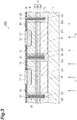
FIG. 3 is a cross-sectional view of a portion of a light detection element shown inFIG. 2 . -
FIG. 4 is a cross-sectional view of a portion of the light detection element shown inFIG. 2 . -
FIG. 5 is a timing diagram for acquiring information relating to a distance to an object. -
FIG. 6 is a cross-sectional view of a portion of a light detection element of a modification example. -
FIG. 7 is another cross-sectional view of the light detection element of the modification example. -
FIG. 8 is a cross-sectional view of a portion of the light detection element of the modification example. -
FIG. 9 is another cross-sectional view of the light detection element of the modification example. - Hereinafter, an embodiment of the present disclosure will be described in detail with reference to the accompanying drawings. Meanwhile, the same or equivalent portions in the drawings are denoted by the same reference numerals and signs, and thus description thereof will not be repeated.
- As shown in
FIG. 1 , a light detection device 1 includes alight detection unit 2, a light source 3, acontrol unit 4, and adisplay unit 5. The light detection device 1 is a device that acquires a distance image of an object OJ (an image including information relating to a distance d to an object OJ) using an indirect TOF scheme. - As shown in
FIG. 2 , thelight detection unit 2 includes a signal processing circuit (signal processing unit) 6 and alight detection element 10A. Thesignal processing circuit 6 includes a voltagesignal generation circuit 61, aCMOS readout circuit 62, avertical scanning circuit 63, acolumn circuit 64, ahorizontal scanning circuit 65, anamplifier 66, and atiming generation circuit 67. In the present embodiment, thelight detection element 10A is an InGaAs area sensor of a rear surface incident type, and is connected by a bump on theCMOS readout circuit 62. - The voltage
signal generation circuit 61 generates a pulse voltage signal and applies the generated signal to thelight detection element 10A. TheCMOS readout circuit 62 is constituted by a plurality of charge amplifiers and the like, and integrates a signal current in each charge amplifier in a case where a detection signal is output from each pixel of thelight detection element 10A. - The
vertical scanning circuit 63 sequentially selects the plurality of charge amplifiers of theCMOS readout circuit 62 for each row. Thecolumn circuit 64 samples and holds a signal voltage integrated in each charge-up of the selected row together with a reset voltage. Thehorizontal scanning circuit 65 sequentially transfers a voltage difference between the signal voltage and the reset voltage sampled and held in thecolumn circuit 64 to theamplifier 66. - The
amplifier 66 amplifies the voltage difference between the signal voltage and the reset voltage sequentially transferred from thecolumn circuit 64, and outputs the amplified voltage difference, as an output voltage signal, to the control unit 4 (seeFIG. 1 ). Thetiming generation circuit 67 controls operation timings of the voltagesignal generation circuit 61, thevertical scanning circuit 63 and thehorizontal scanning circuit 65. Meanwhile, theamplifier 66 is provided in the case of analog output, but an AD converter is provided instead of theamplifier 66 in the case of digital output. - As shown in
FIG. 3 , thelight detection element 10A includes asemiconductor substrate 11 of an n-type (a first conductivity type), alight absorbing layer 12 of an n-type, arelaxation layer 13 of an n-type, acap layer 14 of an n-type, and a plurality ofsemiconductor regions 15 of a p-type (a second conductivity type). Thelight absorbing layer 12 is formed on thesemiconductor substrate 11, for example, by epitaxial growth. Therelaxation layer 13 is formed on thelight absorbing layer 12, for example, by epitaxial growth. Thecap layer 14 is formed on therelaxation layer 13, for example, by epitaxial growth. - The
relaxation layer 13 is constituted by a plurality oflayers layer 12 and thecap layer 14. The bandgap of each of thelayers light absorbing layer 12 and the bandgap of thecap layer 14. In a case where the difference between the bandgap of thelight absorbing layer 12 and the bandgap of thecap layer 14 can be relaxed, therelaxation layer 13 may be constituted by one layer. By providing therelaxation layer 13 in this manner, there is more of tendency for thecap layer 14 to be formed than in a case where thecap layer 14 is formed directly on thelight absorbing layer 12. - The plurality of
semiconductor regions 15 are formed within thecap layer 14, for example, by thermal diffusion, ion implantation, or the like. The plurality ofsemiconductor regions 15 are arranged two-dimensionally (for example, in a matrix) when viewed from the thickness direction of thesemiconductor substrate 11. Each of thesemiconductor regions 15 is formed along the surface of thecap layer 14 located on the opposite side of thesemiconductor substrate 11, and is separated from the surface of thecap layer 14 on thesemiconductor substrate 11 side. Each of thesemiconductor regions 15 forms a pn junction with thecap layer 14, and constitutes a pixel P. A depletion layer D1 is formed around each of thesemiconductor regions 15. Meanwhile, thesemiconductor region 15 is, for example, an impurity region having an impurity concentration of 1 × 1017 cm-3 or greater. - In the present embodiment, the
semiconductor substrate 11 is an n+-InP substrate having a carrier concentration of 0.5 to 5×1018 cm-3 (for example, approximately 1×1018 cm-3), and the thickness thereof is 150 to 300 µm (for example, approximately 200 µm). Thelight absorbing layer 12 is an n--InGaAs layer having a carrier concentration of 3 to 10×1014 cm-3 (for example, approximately 5×1014 cm-3), and the thickness thereof is 1 to 5 µm (for example, approximately 2 µm). Therelaxation layer 13 is an n--InGaAsP layer having a carrier concentration of 0.3 to 5×1015 cm-3 (for example, approximately 1×1015 cm-3), and the thickness thereof is 0.1 to 0.6 µm (for example, approximately 0.2 µm). Thecap layer 14 is an n--InP layer having a carrier concentration of 0.3 to 5×1015 cm-3 (for example, approximately 1×1015 cm-3), and the thickness thereof is 1 to 2 µm (for example, approximately 1.5 µm). Each of thesemiconductor regions 15 is a p+ region having a carrier concentration of 0.1 to 10×1018 cm-3 (for example, approximately 1×1018 cm-3), and the thickness thereof is 0.1 to 1 µm (for example, approximately 0.5 µm). - The
light detection element 10A further includes a plurality offirst electrodes 16 and a plurality ofsecond electrodes 17. Thefirst electrodes 16 and thesecond electrodes 17 are formed on an insulatingfilm 18 formed on the surface of thecap layer 14 located on the opposite side of thesemiconductor substrate 11. Thefirst electrodes 16 and thesecond electrodes 17 are formed of, for example, Ti, Pt, Cr, Ni, Au, an alloy thereof, or the like. The insulatingfilm 18 is, for example, a silicon nitride film, a silicon oxide film, or the like. - Each of the
first electrodes 16 extends into a groove (or through-hole) formed in thelight absorbing layer 12, therelaxation layer 13, thecap layer 14 and the insulatingfilm 18, and electrically contacts thelight absorbing layer 12, therelaxation layer 13 and thecap layer 14. The groove (or through-hole) is formed not to influence the depletion layer D1. Each of thesecond electrodes 17 extends into an opening (or through-hole) formed in the insulatingfilm 18, and electrically contacts one of thesemiconductor regions 15. Since thefirst electrode 16 functions as a common electrode, at least one may be provided for a plurality of pixels P. Since thesecond electrode 17 functions as an individual electrode, one needs to be provided for one pixel P. Meanwhile, in a case where the groove (or through-hole) into which each of thefirst electrodes 16 extends is formed not to influence the depletion layer D1, the groove may reach any of thesemiconductor substrate 11, thelight absorbing layer 12, therelaxation layer 13 and thecap layer 14. - The
light absorbing layer 12, therelaxation layer 13 and thecap layer 14 are provided withpixel separation portions 20. Each of thepixel separation portion 20 extends to pass between pixels P which are next to each other (that is, to pass between thesemiconductor regions 15 which are next to each other). In a case where a plurality of semiconductor regions 10a are arranged in a matrix, thepixel separation portion 20 extends in a lattice shape. - The
pixel separation portion 20 is configured by asemiconductor region 22 of a p-type being formed along the inner surface of agroove 21 formed in thelight absorbing layer 12, therelaxation layer 13 and thecap layer 14. A depletion layer D2 is formed around thesemiconductor region 22. The pixel separation portion 20 (that is, thegroove 21 and the semiconductor region 22) reaches the lateral side of thelight detection element 10A, and thesemiconductor region 22 is short-circuited on the lateral side. Meanwhile, the inner surface of thegroove 21 is covered with the insulatingfilm 18. - In each pixel P, the depletion layer D1 formed around the
semiconductor region 15 does not reach thelight absorbing layer 12 in a case where a reverse bias is not applied between thefirst electrode 16 and the second electrode 17 (in an unbiased state). On the other hand, in a case where a reverse bias of 20 V is applied between thefirst electrode 16 and thesecond electrode 17, the depletion layer D1 exceeds a position amounting to 80% of the thickness of thelight absorbing layer 12 from thecap layer 14 side (a position amounting to 80% of the thickness of thelight absorbing layer 12 from the surface of thelight absorbing layer 12 on thecap layer 14 side with the surface used as a reference) as shown inFIG. 4 . Meanwhile, the wording "a reverse bias is applied or is not applied between thefirst electrode 16 and thesecond electrode 17" is synonymous with "a reverse bias is applied or is not applied to a pn junction where thesemiconductor region 15 serves as thecap layer 14" (the same shall apply hereinafter). - In the present embodiment, since the
first electrode 16 is an n-type side electrode and thesecond electrode 17 is a p-type side electrode, a reverse bias is applied between thefirst electrode 16 and thesecond electrode 17 so that the potential of thesecond electrode 17 is set to -20 V with the potential of thefirst electrode 16 used as a reference. In addition, in the present embodiment, as shown inFIG. 3 , the depletion layer D1 reaches thelayer 13c of therelaxation layer 13 in an unbiased state, but the depletion layer D1 may reach theother layers relaxation layer 13 when not reaching thelight absorbing layer 12 in an unbiased state, or may not reach the relaxation layer 13 (that is, may fall within the cap layer 14). - Here, setting of various parameters of the
light detection element 10A will be described. In a case where the depletion layer D1 reaches thelayer 13c of therelaxation layer 13 in an unbiased state, a reverse bias V required for the depletion layer D1 to reach thelight absorbing layer 12 is represented by Expression (1) assuming that thesemiconductor region 15 is in the state of one-sided abrupt junction.
[Expression 1]
- In Expression (1), W1 is a distance between the depletion layer D1 and the surface of the
layer 13c on thelight absorbing layer 12 side, W2 is the thickness of thelayer 13b, and W3 is the thickness of thelayer 13a. In addition, εr1 is the relative dielectric constant of thelayer 13c, εr2 is the relative dielectric constant of thelayer 13b, and εr3 is the relative dielectric constant of thelayer 13a. N1 is the carrier concentration of thelayer 13c, N2 is the carrier concentration of thelayer 13b, and N3 is the carrier concentration of thelayer 13a. In addition, q is charge, and ε0 is an electric constant. - Therefore, in a case where a reverse bias is not applied between the
first electrode 16 and thesecond electrode 17, a condition in which the depletion layer D1 does not reach thelight absorbing layer 12 is represented by Expression (2).
[Expression 2]
- In addition, in a case where the depletion layer D1 reaches the
layer 13c of therelaxation layer 13 in an unbiased state, a reverse bias V required for the depletion layer D1 to reach a position amounting to X% of the thickness of thelight absorbing layer 12 from thecap layer 14 side (a position amounting to X% of the thickness of thelight absorbing layer 12 from the surface of thelight absorbing layer 12 on thecap layer 14 side with the surface used as a reference) is represented by Expression (3) assuming that thesemiconductor region 15 is in the state of one-sided abrupt junction. In Expression (3), Wab is the thickness of thelight absorbing layer 12, εrab is the relative dielectric constant of thelight absorbing layer 12, and Nab is the carrier concentration of thelight absorbing layer 12.
[Expression 3]
- Therefore, in a case where a reverse bias of 20 V is applied between the
first electrode 16 and thesecond electrode 17, a condition in which the depletion layer D1 exceeds a position amounting to 80% of the thickness of thelight absorbing layer 12 from thecap layer 14 side is represented by Expression (4).
[Expression 4]
- In the present embodiment, various parameters of the
light detection element 10A are set so that Expression (2) and Expression (4) are satisfied. Particularly, in the present embodiment, in a case where a reverse bias of 5 V is applied between thefirst electrode 16 and thesecond electrode 17, the depletion layer D1 reaches a position amounting to 100% of thickness of thelight absorbing layer 12 from thecap layer 14 side. That is, in the present embodiment, various parameters of thelight detection element 10A are set so that Expression (5) is satisfied.
[Expression 5]
- Meanwhile, in a case where the depletion layer D1 does not reach the
relaxation layer 13 in an unbiased state (that is, falls within the cap layer 14), an item of thecap layer 14 may be added to the right sides of Expression (1) to Expression (5). In that case, when therelaxation layer 13 is not present, an item relating to therelaxation layer 13 may be subtracted from the right sides of Expression (1) to Expression (5). In this manner, an item corresponding to each layer may be added to or subtracted from the right sides of Expression (1) to Expression (5) in accordance with the layer structure of thelight detection element 10A or the like. - As shown in
FIG. 1 , the light source 3 outputs pulsed light L to which thelight detection element 10A is sensitive (that is, by which photoelectric conversion can be generated in thelight detection element 10A) at a frequency of 10 KHz or higher. In the present embodiment, the light source 3 is, for example, an infrared LED or the like, and outputs pulsed light L having a wavelength of approximately 1.5 µm. The pulsed light L output from the light source 3 is radiated to the object OJ, and the pulsed light L reflected from the object OJ is incident on thelight detection element 10A. Thecontrol unit 4 controls thelight detection unit 2 and the light source 3, generates a distance image of the object OJ on the basis of an output voltage signal which is output from thelight detection unit 2, and causes thedisplay unit 5 to display the generated distance image. - As described above, in the
light detection element 10A, in a case where a reverse bias is not applied between thefirst electrode 16 and thesecond electrode 17, the depletion layer D1 does not reach thelight absorbing layer 12. Thereby, even when carriers (electrons and holes) have been generated in thelight absorbing layer 12 due to the incidence of the pulsed light L, a current does not flow between thefirst electrode 16 and thesecond electrode 17. That is, for example, a reverse bias is not applied between thefirst electrode 16 and thesecond electrode 17, so that it is possible not to output a detection signal from thelight detection element 10A to thesignal processing circuit 6. On the other hand, in a case where a reverse bias of 20 V is applied between thefirst electrode 16 and thesecond electrode 17, the depletion layer D1 exceeds a position amounting to 80% of the thickness of thelight absorbing layer 12 from thecap layer 14 side. Thereby, in a case where carriers are generated in a region of thelight absorbing layer 12 in which the depletion layer D1 spreads due to the incidence of the pulsed light L, a current flows between thefirst electrode 16 and thesecond electrode 17. That is, for example, a reverse bias of 20 V is applied between thefirst electrode 16 and thesecond electrode 17, so that it is possible to output a detection signal from thelight detection element 10A to thesignal processing circuit 6. Here, the potential difference of 20 V is a potential difference which is not likely to influence the design of the latter-stagesignal processing circuit 6, and is a potential difference by which modulation at a high speed such as on the order of several tens of ns is possible. Thus, according to thelight detection element 10A, it is possible to realize control of output of a detection signal at a high speed with a simple configuration. - Particularly, in the
light detection element 10A, in a case where a reverse bias of 5 V is applied between thefirst electrode 16 and thesecond electrode 17, the depletion layer D1 reaches a position amounting to 100% of the thickness of thelight absorbing layer 12 from thecap layer 14 side. Since thelight detection element 10A is an area sensor of a rear surface incident type for causing light to be incident from thesemiconductor substrate 11 side, the depletion layer D1 reaching the surface of thelight absorbing layer 12 on the light incident side by the application of a reverse bias of 5 V is effective in achieving an improvement in sensitivity and responsiveness. - Meanwhile, an avalanche photodiode is also an element that detects light by the application of a reverse bias, but is basically different from the
light detection element 10A, in that a potential difference as high as, for example, 50 V is required as a reverse bias. In the avalanche photodiode, in order to increase the intensity of an electric field which is applied to the cap layer having a multiplication layer formed thereon, and to decrease the intensity of an electric field which is applied to the light absorbing layer, electric field suppression layer is formed between the light absorbing layer and the cap layer. On the other hand, in thelight detection element 10A, in order to decrease the intensity of an electric field which is applied to thecap layer 14, and to increase the intensity of an electric field which is applied to thelight absorbing layer 12, an electric field suppression layer is not formed between the light absorbinglayer 12 and thecap layer 14. Meanwhile, the potential difference of 50 V is a potential difference that has a tendency to influence the design of a latter-stage circuit such as a CMOS, and is a potential difference by which modulation at a high speed such as on the order of several tens of ns is impossible. - In addition, in the
light detection element 10A, therelaxation layer 13 of an n-type is formed between the light absorbinglayer 12 and thecap layer 14. Thereby, it is possible to smoothly move carriers generated in a region of thelight absorbing layer 12 in which the depletion layer D1 spreads. - In addition, in the
light detection element 10A, the plurality ofsemiconductor regions 15 are arranged two-dimensionally within thecap layer 14 when viewed from the thickness direction of thesemiconductor substrate 11. Thereby, it is possible to acquire a distance image of the object OJ. - In addition, in the
light detection element 10A, thelight absorbing layer 12, therelaxation layer 13 and thecap layer 14 are provided with thepixel separation portion 20. Thereby, it is possible to suppress the generation of crosstalk between pixels P which are next to each other. In addition, even when carriers are generated in thelight absorbing layer 12 in an unbiased state, the carriers are trapped by the depletion layer D2 formed around thesemiconductor region 22. Therefore, on the occasion of being switched from an unbiased state to a reverse bias application state, it is possible to prevent the carriers generated in thelight absorbing layer 12 in an unbiased state from acting on noise. - In addition, in the
light detection element 10A, the carrier concentrations of thelight absorbing layer 12, therelaxation layer 13 and thecap layer 14 are set to be equal to or less than 1×1016 cm-3. Thereby, it is possible to smoothly spread the depletion layer D1 to thelight absorbing layer 12 by the application of a reverse bias having a potential difference of 20 V or lower. - In addition, the light detection device 1 applies a pulse voltage signal between the
light detection element 10A, thefirst electrode 16 and thesecond electrode 17, and includes thesignal processing circuit 6 that acquires a detection signal which is output from thelight detection element 10A and the light source 3 that outputs the pulsed light L to which thelight detection element 10A is sensitive at a frequency of 10 KHz or higher. Thereby, it is possible to appropriately acquire information relating to the distance d to the object OJ as in a calculation example to be described next. - A calculation example of the distance d to the object OJ will be described with reference to
FIG. 5. FIG. 5 shows an intensity signal IOUT of the pulsed light L which is output from the light source 3, an intensity signal IIN of the pulsed light L which is reflected from the object OJ and is incident on thelight detection element 10A, a pulse voltage signal V1IN which is applied to thelight detection element 10A (specifically, between thefirst electrode 16 and the second electrode 17) in a first phase, a pulse voltage signal V2IN which is applied to thelight detection element 10A in a second phase, and a pulse voltage signal V3IN which is applied to thelight detection element 10A in a third phase. Meanwhile, in this calculation example, attention is focused on any one pixel P. - In the first phase, an output voltage signal V1OUT is acquired in a state in which the pulsed light L is output from the light source 3 with the intensity signal IOUT and the pulse voltage signal V1IN is applied to the
light detection element 10A. The pulse width T of the intensity signal IOUT is set in accordance with a distance to be measured like, for example, 30 ns (measurable distance: ∼ 4.5 m), 40 ns (measurable distance: ∼ 6.0 m), or 60 ns (measurable distance: ∼ 9.0 m). The pulse voltage signal V1IN is a voltage signal in which a first voltage VL at which the depletion layer D1 does not reach thelight absorbing layer 12 and a second voltage VH at which the depletion layer D1 reaches thelight absorbing layer 12 are alternately repeated, and is a voltage signal which has the same period, pulse width and phase as the intensity signal IOUT. The first voltage VL is 0 V in the present embodiment. The second voltage VH is a voltage at which the depletion layer D1 reaches a position amounting to 100% of the thickness of thelight absorbing layer 12 from thecap layer 14 side, and is 5 V in the present embodiment. In this case, since thelight detection element 10A outputs a detection signal only for a period in which the second voltage VH is applied, the output voltage signal V1OUT corresponds to an integrated value of the amount of charge Q1 at a portion where the pulse of the intensity signal IIN and the pulse of the pulse voltage signal V1IN overlap each other. - In the second phase, an output voltage signal V2OUT is acquired in a state in which the pulsed light L is output from the light source 3 with the intensity signal IOUT and the pulse voltage signal V2IN is applied to the
light detection element 10A. The pulse voltage signal V2IN is the same voltage signal as the pulse voltage signal V1IN except that its phase is shifted by 180°. In this case, since thelight detection element 10A outputs a detection signal only for a period in which the second voltage VH is applied, the output voltage signal V2OUT corresponds to an integrated value of the amount of charge Q2 at a portion where the pulse of the intensity signal IIN and the pulse of the pulse voltage signal V2IN overlap each other. - In the third phase, an output voltage signal V3OUT is acquired in a state in which the pulsed light L is not output from the light source 3 and the pulse voltage signal V3IN is applied to the
light detection element 10A. In this case, since thelight detection element 10A outputs a detection signal only for a period in which the second voltage VH is applied, the output voltage signal V3OUT corresponds to an integrated value of the amount of charge at a portion where the intensity signal of disturbance light, if any, and the pulse of the pulse voltage signal V3IN overlap each other. - In a case where the first phase, the second phase and the third phase described above are performed for each pixel P, the
control unit 4 calculates the distance d to the object OJ on the basis of the output voltage signals V1OUT, V2OUT, and V3OUT for each pixel P. The distance d is represented by Expression (6). In Expression (6), c is the speed of light.
[Expression 6]
- As described above, in the light detection device 1, it is possible to bring the
light detection element 10A into switching operation (fluctuation operation) in the order of several tens of ns. In addition, in the light detection device 1, the second voltage VH of each of the output voltage signals V1OUT and V2OUT is a voltage at which the depletion layer D1 reaches a position amounting to 100% of the thickness of thelight absorbing layer 12 from thecap layer 14 side. Thereby, it is possible to prevent carriers generated in a region of thelight absorbing layer 12 in which the depletion layer D1 does not spread from being detected as a delay component, and to prevent the accuracy of calculation of the distance d from deteriorating. In addition, in the light detection device 1, the light source 3 is a light source that emits the pulsed light L having a wavelength of approximately 1.5 µm, and the light detection element 10 is an InGaAs area sensor with sufficient sensitivity to the pulsed light L having a wavelength of approximately 1.5 µm. Thereby, it becomes easier to acquire a distance image of the object OJ, for example, even in fog or smoke. Meanwhile, the above-described calculation example is merely an example, and the information relating to the distance d to the object OJ can be acquired by various known calculations. In addition, the second voltage VH may be a voltage of 20 V or lower (preferably a voltage of 10 V or lower, more preferably a voltage of 5 V or lower). In that case, it is possible to more reliably achieve an improvement in sensitivity and responsiveness in the light detection device 1. - The present disclosure is not limited to the above-described embodiment. For example, the
light detection element 10A may be configured as a linear sensor in which the plurality ofsemiconductor regions 15 are arranged one-dimensionally within thecap layer 14.FIGS. 6 and7 show alight detection element 10B configured as an InGaAs linear sensor of a rear surface incident type. Meanwhile,FIG. 6 is a cross-sectional view of a portion of thelight detection element 10B along a surface parallel to the arrangement direction of the plurality of semiconductor regions 15 (hereinafter simply referred to as the "arrangement direction"), andFIG. 7 is a cross-sectional view of thelight detection element 10B along a surface perpendicular to the arrangement direction. - The
light detection element 10B is mainly different from the above-described thelight detection element 10A, in that therelaxation layer 13 of an n-type is not formed between the light absorbinglayer 12 and thecap layer 14, and that asemiconductor region 23 of a p-type is formed therebetween. In thelight detection element 10B, as shown inFIG. 7 , in a width direction perpendicular to both the thickness direction of thesemiconductor substrate 11 and the arrangement direction (hereinafter simply referred to as a "width direction"), the width of thecap layer 14 is smaller than the width of thesemiconductor substrate 11, and the width of thelight absorbing layer 12 is the same as the width of thesemiconductor substrate 11. Thesemiconductor region 23 is formed along the lateral sides of thecap layer 14 facing each other in the width direction, and an area on which thecap layer 14 is not formed, the area is a part of the surface of thelight absorbing layer 12 on the opposite side of thesemiconductor substrate 11. Thesemiconductor region 23 is covered with the insulatingfilm 18. - In the
light detection element 10B, as shown inFIGS. 8 and9 , only in a case where a reverse bias of 20 V is applied between thefirst electrode 16 and thesecond electrode 17, the depletion layer D1 exceeds a position amounting to 80% of the thickness of thelight absorbing layer 12 from thecap layer 14 side. Thus, according to thelight detection element 10B, similarly to the above-described thelight detection element 10A, it is possible to realize control of output of a detection signal at a high speed with a simple configuration. - In addition, in the
light detection element 10B, carriers generated in thelight absorbing layer 12 in an unbiased state are trapped by not only the depletion layer D2 formed around thesemiconductor region 22 of thepixel separation portion 20, but also a depletion layer D3 formed around thesemiconductor region 23. Therefore, on the occasion of being switched from an unbiased state to a reverse bias application state, it is possible to prevent the carriers generated in thelight absorbing layer 12 in an unbiased state from acting on noise. - In addition, in the
light detection element 10B, the width of thecap layer 14 is smaller than the width of thesemiconductor substrate 11 in the width direction. Thereby, it is possible to prevent carriers generated in a region around a pn junction region (a region of a pixel P) from acting on noise. Meanwhile, the width of thelight absorbing layer 12 and the width of thecap layer 14 may be smaller than the width of thesemiconductor substrate 11 in the width direction. In that case, it is possible to more reliably prevent carriers generated in a region around a pn junction region from acting on noise. - In addition, in the
light detection element 10A shown inFIG. 3 , therelaxation layer 13 of an n-type may not be formed between the light absorbinglayer 12 and thecap layer 14. On the contrary, in thelight detection element 10B shown inFIGS. 6 and7 , therelaxation layer 13 of an n-type may be formed between the light absorbinglayer 12 and thecap layer 14. In a case where therelaxation layer 13 is not formed, and thelight absorbing layer 12 and thecap layer 14 are in contact with each other, it is possible to possible to make a reverse bias for the depletion layer D1 to exceed a position amounting to at least 50% of the thickness of thelight absorbing layer 12 from thecap layer 14 side. Meanwhile, in thelight detection element 10B shown inFIGS. 6 and7 , in a case where therelaxation layer 13 is formed between the light absorbinglayer 12 and thecap layer 14, the width of therelaxation layer 13 and the width of thecap layer 14 may be smaller than the width of thesemiconductor substrate 11 in the width direction, or the width of thelight absorbing layer 12, the width of therelaxation layer 13 and the width of thecap layer 14 may be smaller than the width of thesemiconductor substrate 11 in the width direction. In those cases, it is possible to more reliably prevent carriers generated in a region around a pn junction region from acting on noise. - In addition, in the
light detection element 10A shown inFIG. 3 , thepixel separation portion 20 may not be provided. Similarly, in thelight detection element 10B shown inFIGS. 6 and7 , thepixel separation portion 20 may not be provided. In addition, in thelight detection element 10B shown inFIGS. 6 and7 , thesemiconductor region 23 may not be formed. - In addition, in any of the above-described
light detection elements first electrode 16 and thesecond electrode 17, the depletion layer D1 may exceed a position amounting to 50% of the thickness of thelight absorbing layer 12 from thecap layer 14 side (a position amounting to 50% of the thickness of thelight absorbing layer 12 from the surface of thelight absorbing layer 12 on thecap layer 14 side with the surface used as a reference). To which position the depletion layer D1 is spread in a range of 50% to 100% of thickness of thelight absorbing layer 12 from thecap layer 14 side by the application of a reverse bias of 20 V is determined in accordance with the wavelength of light to be detected, the incident direction of light to be detected, or the like. - In addition, both of the above-described
light detection elements first electrode 16 is formed on, for example, the surface of thesemiconductor substrate 11 on the opposite side of thelight absorbing layer 12. In addition, for example, an opening for causing light to be detected to be incident on thelight absorbing layer 12 is formed in thesecond electrode 17. In a case where each of thelight detection elements layer 12 be larger than the bandgap of thelight absorbing layer 12 from the viewpoint of the suppression of light absorption in the layer. Meanwhile, even in a case where each of thelight detection elements layer 12 be larger than the bandgap of thelight absorbing layer 12 from the viewpoint of the suppression of a dark current. - In addition, in any of the above-described
light detection elements first electrode 16 serves as a p-type side electrode, and thesecond electrode 17 serves as an n-type side electrode, a reverse bias is applied between thefirst electrode 16 and thesecond electrode 17 so that the potential of thesecond electrode 17 is set to a positive potential with the potential of thefirst electrode 16 used as a reference. Meanwhile, as described above, in a case where thesemiconductor substrate 11, thelight absorbing layer 12, therelaxation layer 13 and thecap layer 14 are an n-type, and thesemiconductor region 15 is a p-type, it is possible to secure facilitation of manufacturing of thelight detection elements - In addition, in any of the above-described
light detection elements light absorption layer 12 and thecap layer 14 or in thecap layer 14 so that thesemiconductor regions 15 are reliably contained in thecap layer 14 at the time of manufacturing. In addition, in any of the above-describedlight detection elements light absorption layer 12 and thecap layer 14 so that the depletion layer D1 does not reach thelight absorbing layer 12 due to a variation during manufacturing or the like in spite of being in an unbiased state. In addition, in any of the above-describedlight detection elements cap layer 14. - In addition, both of the above-described
light detection elements semiconductor region 15 is formed within thecap layer 14. In that case, it is also possible to realize control of output of a detection signal at a high speed with a simple configuration. In addition, in that case, it is configured as the light detection device 1, so that it is also possible to acquire information relating to the distance d to the object OJ. - In addition, various materials and shapes can be applied to the configurations of the above-described
light detection elements light detection elements - In addition, the light detection device 1 may not include the light source 3. An example of the light detection device 1 in that case to be exemplified includes an infrared image sensor having a global shutter operation (high-speed shutter operation) required for detecting high-speed objects and signals, or the like.
- 1: light detection device, 3: light source, 6: signal processing circuit (signal processing unit), 10A, 10B: light detection element, 11: semiconductor substrate, 12: light absorbing layer, 13: relaxation layer, 14: cap layer, 15: semiconductor region, 16: first electrode, 17: second electrode, D1: depletion layer
Claims (15)
- A light detection element comprising:a semiconductor substrate;a light absorbing layer of a first conductivity type formed on the semiconductor substrate;a cap layer of a first conductivity type formed on the light absorbing layer; anda semiconductor region of a second conductivity type formed within the cap layer and forming a pn junction with the cap layer,wherein a depletion layer formed around the semiconductor region does not reach the light absorbing layer in a case where a reverse bias is not applied to the pn junction, and exceeds a position amounting to 50% of a thickness of the light absorbing layer from the cap layer side in a case where a reverse bias of 20 V is applied to the pn junction.
- The light detection element according to claim 1, wherein the depletion layer exceeds a position amounting to 80% of the thickness of the light absorbing layer from the cap layer side in a case where a reverse bias of 20 V is applied to the pn junction.
- The light detection element according to claim 1 or 2, further comprising a relaxation layer of a first conductivity type formed between the light absorbing layer and the cap layer.
- The light detection element according to claim 1 or 2, wherein the light absorbing layer and the cap layer are in contact with each other.
- The light detection element according to any one of claims 1 to 4, wherein a plurality of semiconductor regions, each of which is the semiconductor region, are formed within the cap layer, and are arranged one-dimensionally or two-dimensionally when viewed from a thickness direction of the semiconductor substrate.
- The light detection element according to any one of claims 1 to 5, wherein a plurality of semiconductor regions, each of which is the semiconductor region, are formed within the cap layer, and are arranged one-dimensionally when viewed from a thickness direction of the semiconductor substrate, and
a width of the cap layer is smaller than a width of the semiconductor substrate in a width direction perpendicular to both the thickness direction of the semiconductor substrate and an arrangement direction of the semiconductor regions. - The light detection element according to claim 6, wherein a width of the light absorbing layer is smaller than the width of the semiconductor substrate in the width direction.
- The light detection element according to any one of claims 1 to 7, wherein the first conductivity type is an n-type, and the second conductivity type is a p-type.
- A light detection device comprising:the light detection element according to any one of claims 1 to 8; anda signal processing unit configured to apply a pulse voltage signal to the pn junction, and to acquire a detection signal output from the light detection element,wherein the pulse voltage signal is a voltage signal in which a first voltage at which the depletion layer does not reach the light absorbing layer and a second voltage at which the depletion layer reaches the light absorbing layer are alternately repeated.
- The light detection device according to claim 9, wherein the second voltage is a voltage at which the depletion layer reaches a position amounting to 100% of the thickness of the light absorbing layer from the cap layer side.
- The light detection device according to claim 9 or 10, wherein the second voltage is a voltage of 20 V or lower.
- The light detection device according to any one of claims 9 to 11, wherein the second voltage is a voltage of 10 V or lower.
- The light detection device according to any one of claims 9 to 12, wherein the second voltage is a voltage of 5 V or lower.
- The light detection device according to any one of claim 9 to 13, further comprising a light source configured to output pulsed light to which the light detection element is sensitive.
- The light detection device according to claim 14, wherein the light source is configured to output the pulsed light at a frequency of 10 KHz or higher.
Applications Claiming Priority (2)
| Application Number | Priority Date | Filing Date | Title |
|---|---|---|---|
| JP2018195146A JP6641442B1 (en) | 2018-10-16 | 2018-10-16 | Photodetector and photodetector |
| PCT/JP2019/027418 WO2020079897A1 (en) | 2018-10-16 | 2019-07-10 | Light detection element and light detection device |
Publications (2)
| Publication Number | Publication Date |
|---|---|
| EP3869570A1 true EP3869570A1 (en) | 2021-08-25 |
| EP3869570A4 EP3869570A4 (en) | 2022-07-06 |
Family
ID=69320968
Family Applications (1)
| Application Number | Title | Priority Date | Filing Date |
|---|---|---|---|
| EP19873708.2A Pending EP3869570A4 (en) | 2018-10-16 | 2019-07-10 | LIGHT SENSING ELEMENT AND LIGHT SENSING DEVICE |
Country Status (6)
| Country | Link |
|---|---|
| US (1) | US11450705B2 (en) |
| EP (1) | EP3869570A4 (en) |
| JP (1) | JP6641442B1 (en) |
| KR (1) | KR102739915B1 (en) |
| CN (1) | CN112868108B (en) |
| WO (1) | WO2020079897A1 (en) |
Families Citing this family (1)
| Publication number | Priority date | Publication date | Assignee | Title |
|---|---|---|---|---|
| CN114323089B (en) * | 2020-10-12 | 2025-02-25 | 群创光电股份有限公司 | Light detection element |
Family Cites Families (18)
| Publication number | Priority date | Publication date | Assignee | Title |
|---|---|---|---|---|
| GB2078440B (en) * | 1980-03-31 | 1984-04-18 | Nippon Telegraph & Telephone | An optoelectronic switch |
| JP2708409B2 (en) * | 1986-06-20 | 1998-02-04 | 株式会社日立製作所 | Semiconductor light receiving element and method of manufacturing the same |
| JPH03230582A (en) * | 1990-02-06 | 1991-10-14 | Mitsubishi Electric Corp | Semiconductor light receiving device |
| US6515740B2 (en) * | 2000-11-09 | 2003-02-04 | Canesta, Inc. | Methods for CMOS-compatible three-dimensional image sensing using quantum efficiency modulation |
| JP2002231992A (en) * | 2001-02-02 | 2002-08-16 | Toshiba Corp | Semiconductor light receiving element |
| DE10112833C1 (en) * | 2001-03-16 | 2003-03-13 | Hilti Ag | Method and device for electro-optical distance measurement |
| JP2004241588A (en) * | 2003-02-05 | 2004-08-26 | Matsushita Electric Ind Co Ltd | Light receiving element, method of manufacturing the same, and optical module using the light receiving element |
| KR20060002239A (en) * | 2004-07-01 | 2006-01-09 | 삼성전자주식회사 | Laser power controller |
| US7368762B2 (en) * | 2005-01-06 | 2008-05-06 | Teledyne Licensing, Llc | Heterojunction photodiode |
| JP5015494B2 (en) * | 2006-05-22 | 2012-08-29 | 住友電工デバイス・イノベーション株式会社 | Semiconductor photo detector |
| JP5558999B2 (en) | 2009-11-24 | 2014-07-23 | 浜松ホトニクス株式会社 | Distance sensor and distance image sensor |
| DE102010043822B4 (en) * | 2010-11-12 | 2014-02-13 | Namlab Ggmbh | Photodiode and photodiode array and method for their operation |
| US9541386B2 (en) * | 2012-03-21 | 2017-01-10 | Semiconductor Energy Laboratory Co., Ltd. | Distance measurement device and distance measurement system |
| JP6236758B2 (en) * | 2012-10-09 | 2017-11-29 | 株式会社豊田中央研究所 | Optical distance measuring device |
| JP6112472B2 (en) * | 2013-01-15 | 2017-04-12 | 住友電気工業株式会社 | Manufacturing method of light receiving device |
| US20140217540A1 (en) * | 2013-02-04 | 2014-08-07 | Teledyne Scientific & Imaging, Llc | Fully depleted diode passivation active passivation architecture |
| CN110431441B (en) * | 2017-03-19 | 2023-09-15 | 科维塔公司 | System and method for modulated image capture |
| CN107799543A (en) * | 2017-11-03 | 2018-03-13 | 德淮半导体有限公司 | The manufacture method of contact-type image sensor |
-
2018
- 2018-10-16 JP JP2018195146A patent/JP6641442B1/en active Active
-
2019
- 2019-07-10 WO PCT/JP2019/027418 patent/WO2020079897A1/en not_active Ceased
- 2019-07-10 KR KR1020217011293A patent/KR102739915B1/en active Active
- 2019-07-10 CN CN201980068249.7A patent/CN112868108B/en active Active
- 2019-07-10 EP EP19873708.2A patent/EP3869570A4/en active Pending
-
2020
- 2020-01-30 US US16/777,291 patent/US11450705B2/en active Active
Also Published As
| Publication number | Publication date |
|---|---|
| CN112868108B (en) | 2024-12-20 |
| JP6641442B1 (en) | 2020-02-05 |
| KR102739915B1 (en) | 2024-12-10 |
| CN112868108A (en) | 2021-05-28 |
| WO2020079897A1 (en) | 2020-04-23 |
| JP2020064933A (en) | 2020-04-23 |
| EP3869570A4 (en) | 2022-07-06 |
| US20200168656A1 (en) | 2020-05-28 |
| KR20210072003A (en) | 2021-06-16 |
| US11450705B2 (en) | 2022-09-20 |
Similar Documents
| Publication | Publication Date | Title |
|---|---|---|
| JP5585903B2 (en) | Distance image sensor and method for generating imaging signal by time-of-flight method | |
| US11330205B2 (en) | Photosensor, image sensor, and photosensor driving method | |
| US9743026B2 (en) | Semiconductor photodetector | |
| EP2731148B1 (en) | Photodiode array, reference voltage determining method, and recommended operation voltage determining method | |
| EP2506036B1 (en) | Range sensor and range image sensor | |
| JP5297276B2 (en) | Photodiode array | |
| JP7366558B2 (en) | Sensor and distance measuring device | |
| US8592863B2 (en) | Photodetector with internal gain and detector comprising an array of such photodetectors | |
| US20210193707A1 (en) | Back-illuminated semiconductor light detecting device | |
| US7053458B2 (en) | Suppressing radiation charges from reaching dark signal sensor | |
| US20230358534A1 (en) | Photodetector and distance measuring system | |
| US11450705B2 (en) | Light detection element and light detection device | |
| JP2009238985A (en) | Semiconductor imaging element, and method of manufacturing the same | |
| EP1668708B1 (en) | Optoelectronic detector with multiple readout nodes and its use thereof | |
| JP6847878B2 (en) | Photodetector, photodetector and lidar device | |
| US12009439B2 (en) | Photodiode and method for operating a photodiode | |
| US20230035346A1 (en) | Light detection device and method for driving photosensor | |
| US11251317B2 (en) | Photodiode including an additional depletion region for sensitivity control and method of creating the same | |
| KR20240000916A (en) | SINGLE PHOTON DETECTION ELEMENT, ELECTRONIC DEVICE, AND LiDAR DEVICE | |
| US9625587B2 (en) | Device for reading radiological images | |
| Zappa et al. | Single-photon avalanche diode arrays and CMOS microelectronics for counting, timing, and imaging quantum events | |
| US20230027464A1 (en) | Distance measurement device, and method for driving distance measurement sensor | |
| RU178899U1 (en) | Two-channel photodetector | |
| KR20060093445A (en) | Quantum Structure Infrared Receiver |
Legal Events
| Date | Code | Title | Description |
|---|---|---|---|
| STAA | Information on the status of an ep patent application or granted ep patent |
Free format text: STATUS: THE INTERNATIONAL PUBLICATION HAS BEEN MADE |
|
| PUAI | Public reference made under article 153(3) epc to a published international application that has entered the european phase |
Free format text: ORIGINAL CODE: 0009012 |
|
| STAA | Information on the status of an ep patent application or granted ep patent |
Free format text: STATUS: REQUEST FOR EXAMINATION WAS MADE |
|
| 17P | Request for examination filed |
Effective date: 20210202 |
|
| AK | Designated contracting states |
Kind code of ref document: A1 Designated state(s): AL AT BE BG CH CY CZ DE DK EE ES FI FR GB GR HR HU IE IS IT LI LT LU LV MC MK MT NL NO PL PT RO RS SE SI SK SM TR |
|
| DAV | Request for validation of the european patent (deleted) | ||
| DAX | Request for extension of the european patent (deleted) | ||
| A4 | Supplementary search report drawn up and despatched |
Effective date: 20220608 |
|
| RIC1 | Information provided on ipc code assigned before grant |
Ipc: G01S 17/08 20060101ALI20220601BHEP Ipc: H01L 31/10 20060101ALI20220601BHEP Ipc: H01L 27/146 20060101AFI20220601BHEP |
|
| STAA | Information on the status of an ep patent application or granted ep patent |
Free format text: STATUS: EXAMINATION IS IN PROGRESS |
|
| 17Q | First examination report despatched |
Effective date: 20240626 |