EP3869541A2 - Integrated circuit and electronic device comprising a plurality of integrated circuits electrically coupled through a synchronization signal - Google Patents
Integrated circuit and electronic device comprising a plurality of integrated circuits electrically coupled through a synchronization signal Download PDFInfo
- Publication number
- EP3869541A2 EP3869541A2 EP21153537.2A EP21153537A EP3869541A2 EP 3869541 A2 EP3869541 A2 EP 3869541A2 EP 21153537 A EP21153537 A EP 21153537A EP 3869541 A2 EP3869541 A2 EP 3869541A2
- Authority
- EP
- European Patent Office
- Prior art keywords
- integrated circuit
- solder balls
- electronic device
- support
- master
- Prior art date
- Legal status (The legal status is an assumption and is not a legal conclusion. Google has not performed a legal analysis and makes no representation as to the accuracy of the status listed.)
- Withdrawn
Links
Images



Classifications
-
- H—ELECTRICITY
- H10—SEMICONDUCTOR DEVICES; ELECTRIC SOLID-STATE DEVICES NOT OTHERWISE PROVIDED FOR
- H10W—GENERIC PACKAGES, INTERCONNECTIONS, CONNECTORS OR OTHER CONSTRUCTIONAL DETAILS OF DEVICES COVERED BY CLASS H10
- H10W44/00—Electrical arrangements for controlling or matching impedance
- H10W44/20—Electrical arrangements for controlling or matching impedance at high-frequency [HF] or radio frequency [RF]
-
- H—ELECTRICITY
- H10—SEMICONDUCTOR DEVICES; ELECTRIC SOLID-STATE DEVICES NOT OTHERWISE PROVIDED FOR
- H10W—GENERIC PACKAGES, INTERCONNECTIONS, CONNECTORS OR OTHER CONSTRUCTIONAL DETAILS OF DEVICES COVERED BY CLASS H10
- H10W70/00—Package substrates; Interposers; Redistribution layers [RDL]
- H10W70/60—Insulating or insulated package substrates; Interposers; Redistribution layers
-
- H—ELECTRICITY
- H10—SEMICONDUCTOR DEVICES; ELECTRIC SOLID-STATE DEVICES NOT OTHERWISE PROVIDED FOR
- H10W—GENERIC PACKAGES, INTERCONNECTIONS, CONNECTORS OR OTHER CONSTRUCTIONAL DETAILS OF DEVICES COVERED BY CLASS H10
- H10W70/00—Package substrates; Interposers; Redistribution layers [RDL]
- H10W70/60—Insulating or insulated package substrates; Interposers; Redistribution layers
- H10W70/611—Insulating or insulated package substrates; Interposers; Redistribution layers for connecting multiple chips together
-
- H—ELECTRICITY
- H10—SEMICONDUCTOR DEVICES; ELECTRIC SOLID-STATE DEVICES NOT OTHERWISE PROVIDED FOR
- H10W—GENERIC PACKAGES, INTERCONNECTIONS, CONNECTORS OR OTHER CONSTRUCTIONAL DETAILS OF DEVICES COVERED BY CLASS H10
- H10W70/00—Package substrates; Interposers; Redistribution layers [RDL]
- H10W70/60—Insulating or insulated package substrates; Interposers; Redistribution layers
- H10W70/62—Insulating or insulated package substrates; Interposers; Redistribution layers characterised by their interconnections
- H10W70/65—Shapes or dispositions of interconnections
-
- H—ELECTRICITY
- H10—SEMICONDUCTOR DEVICES; ELECTRIC SOLID-STATE DEVICES NOT OTHERWISE PROVIDED FOR
- H10W—GENERIC PACKAGES, INTERCONNECTIONS, CONNECTORS OR OTHER CONSTRUCTIONAL DETAILS OF DEVICES COVERED BY CLASS H10
- H10W72/00—Interconnections or connectors in packages
- H10W72/20—Bump connectors, e.g. solder bumps or copper pillars; Dummy bumps; Thermal bumps
-
- H—ELECTRICITY
- H10—SEMICONDUCTOR DEVICES; ELECTRIC SOLID-STATE DEVICES NOT OTHERWISE PROVIDED FOR
- H10W—GENERIC PACKAGES, INTERCONNECTIONS, CONNECTORS OR OTHER CONSTRUCTIONAL DETAILS OF DEVICES COVERED BY CLASS H10
- H10W90/00—Package configurations
-
- H—ELECTRICITY
- H10—SEMICONDUCTOR DEVICES; ELECTRIC SOLID-STATE DEVICES NOT OTHERWISE PROVIDED FOR
- H10W—GENERIC PACKAGES, INTERCONNECTIONS, CONNECTORS OR OTHER CONSTRUCTIONAL DETAILS OF DEVICES COVERED BY CLASS H10
- H10W90/00—Package configurations
- H10W90/701—Package configurations characterised by the relative positions of pads or connectors relative to package parts
-
- H—ELECTRICITY
- H10—SEMICONDUCTOR DEVICES; ELECTRIC SOLID-STATE DEVICES NOT OTHERWISE PROVIDED FOR
- H10W—GENERIC PACKAGES, INTERCONNECTIONS, CONNECTORS OR OTHER CONSTRUCTIONAL DETAILS OF DEVICES COVERED BY CLASS H10
- H10W44/00—Electrical arrangements for controlling or matching impedance
- H10W44/20—Electrical arrangements for controlling or matching impedance at high-frequency [HF] or radio frequency [RF]
- H10W44/203—Electrical connections
- H10W44/216—Waveguides, e.g. strip lines
-
- H—ELECTRICITY
- H10—SEMICONDUCTOR DEVICES; ELECTRIC SOLID-STATE DEVICES NOT OTHERWISE PROVIDED FOR
- H10W—GENERIC PACKAGES, INTERCONNECTIONS, CONNECTORS OR OTHER CONSTRUCTIONAL DETAILS OF DEVICES COVERED BY CLASS H10
- H10W44/00—Electrical arrangements for controlling or matching impedance
- H10W44/20—Electrical arrangements for controlling or matching impedance at high-frequency [HF] or radio frequency [RF]
- H10W44/241—Electrical arrangements for controlling or matching impedance at high-frequency [HF] or radio frequency [RF] for passive devices or passive elements
- H10W44/248—Electrical arrangements for controlling or matching impedance at high-frequency [HF] or radio frequency [RF] for passive devices or passive elements for antennas
-
- H—ELECTRICITY
- H10—SEMICONDUCTOR DEVICES; ELECTRIC SOLID-STATE DEVICES NOT OTHERWISE PROVIDED FOR
- H10W—GENERIC PACKAGES, INTERCONNECTIONS, CONNECTORS OR OTHER CONSTRUCTIONAL DETAILS OF DEVICES COVERED BY CLASS H10
- H10W44/00—Electrical arrangements for controlling or matching impedance
- H10W44/20—Electrical arrangements for controlling or matching impedance at high-frequency [HF] or radio frequency [RF]
- H10W44/251—Electrical arrangements for controlling or matching impedance at high-frequency [HF] or radio frequency [RF] for monolithic microwave integrated circuits [MMIC]
-
- H—ELECTRICITY
- H10—SEMICONDUCTOR DEVICES; ELECTRIC SOLID-STATE DEVICES NOT OTHERWISE PROVIDED FOR
- H10W—GENERIC PACKAGES, INTERCONNECTIONS, CONNECTORS OR OTHER CONSTRUCTIONAL DETAILS OF DEVICES COVERED BY CLASS H10
- H10W70/00—Package substrates; Interposers; Redistribution layers [RDL]
- H10W70/60—Insulating or insulated package substrates; Interposers; Redistribution layers
- H10W70/62—Insulating or insulated package substrates; Interposers; Redistribution layers characterised by their interconnections
- H10W70/63—Vias, e.g. via plugs
-
- H—ELECTRICITY
- H10—SEMICONDUCTOR DEVICES; ELECTRIC SOLID-STATE DEVICES NOT OTHERWISE PROVIDED FOR
- H10W—GENERIC PACKAGES, INTERCONNECTIONS, CONNECTORS OR OTHER CONSTRUCTIONAL DETAILS OF DEVICES COVERED BY CLASS H10
- H10W72/00—Interconnections or connectors in packages
- H10W72/071—Connecting or disconnecting
- H10W72/072—Connecting or disconnecting of bump connectors
-
- H—ELECTRICITY
- H10—SEMICONDUCTOR DEVICES; ELECTRIC SOLID-STATE DEVICES NOT OTHERWISE PROVIDED FOR
- H10W—GENERIC PACKAGES, INTERCONNECTIONS, CONNECTORS OR OTHER CONSTRUCTIONAL DETAILS OF DEVICES COVERED BY CLASS H10
- H10W72/00—Interconnections or connectors in packages
- H10W72/071—Connecting or disconnecting
- H10W72/072—Connecting or disconnecting of bump connectors
- H10W72/07251—Connecting or disconnecting of bump connectors characterised by changes in properties of the bump connectors during connecting
- H10W72/07254—Connecting or disconnecting of bump connectors characterised by changes in properties of the bump connectors during connecting changes in dispositions
-
- H—ELECTRICITY
- H10—SEMICONDUCTOR DEVICES; ELECTRIC SOLID-STATE DEVICES NOT OTHERWISE PROVIDED FOR
- H10W—GENERIC PACKAGES, INTERCONNECTIONS, CONNECTORS OR OTHER CONSTRUCTIONAL DETAILS OF DEVICES COVERED BY CLASS H10
- H10W72/00—Interconnections or connectors in packages
- H10W72/071—Connecting or disconnecting
- H10W72/073—Connecting or disconnecting of die-attach connectors
-
- H—ELECTRICITY
- H10—SEMICONDUCTOR DEVICES; ELECTRIC SOLID-STATE DEVICES NOT OTHERWISE PROVIDED FOR
- H10W—GENERIC PACKAGES, INTERCONNECTIONS, CONNECTORS OR OTHER CONSTRUCTIONAL DETAILS OF DEVICES COVERED BY CLASS H10
- H10W72/00—Interconnections or connectors in packages
- H10W72/071—Connecting or disconnecting
- H10W72/075—Connecting or disconnecting of bond wires
- H10W72/07551—Connecting or disconnecting of bond wires characterised by changes in properties of the bond wires during the connecting
- H10W72/07554—Connecting or disconnecting of bond wires characterised by changes in properties of the bond wires during the connecting changes in dispositions
-
- H—ELECTRICITY
- H10—SEMICONDUCTOR DEVICES; ELECTRIC SOLID-STATE DEVICES NOT OTHERWISE PROVIDED FOR
- H10W—GENERIC PACKAGES, INTERCONNECTIONS, CONNECTORS OR OTHER CONSTRUCTIONAL DETAILS OF DEVICES COVERED BY CLASS H10
- H10W72/00—Interconnections or connectors in packages
- H10W72/20—Bump connectors, e.g. solder bumps or copper pillars; Dummy bumps; Thermal bumps
- H10W72/241—Dispositions, e.g. layouts
-
- H—ELECTRICITY
- H10—SEMICONDUCTOR DEVICES; ELECTRIC SOLID-STATE DEVICES NOT OTHERWISE PROVIDED FOR
- H10W—GENERIC PACKAGES, INTERCONNECTIONS, CONNECTORS OR OTHER CONSTRUCTIONAL DETAILS OF DEVICES COVERED BY CLASS H10
- H10W72/00—Interconnections or connectors in packages
- H10W72/20—Bump connectors, e.g. solder bumps or copper pillars; Dummy bumps; Thermal bumps
- H10W72/241—Dispositions, e.g. layouts
- H10W72/247—Dispositions of multiple bumps
- H10W72/248—Top-view layouts, e.g. mirror arrays
-
- H—ELECTRICITY
- H10—SEMICONDUCTOR DEVICES; ELECTRIC SOLID-STATE DEVICES NOT OTHERWISE PROVIDED FOR
- H10W—GENERIC PACKAGES, INTERCONNECTIONS, CONNECTORS OR OTHER CONSTRUCTIONAL DETAILS OF DEVICES COVERED BY CLASS H10
- H10W72/00—Interconnections or connectors in packages
- H10W72/20—Bump connectors, e.g. solder bumps or copper pillars; Dummy bumps; Thermal bumps
- H10W72/251—Materials
- H10W72/252—Materials comprising solid metals or solid metalloids, e.g. PbSn, Ag or Cu
-
- H—ELECTRICITY
- H10—SEMICONDUCTOR DEVICES; ELECTRIC SOLID-STATE DEVICES NOT OTHERWISE PROVIDED FOR
- H10W—GENERIC PACKAGES, INTERCONNECTIONS, CONNECTORS OR OTHER CONSTRUCTIONAL DETAILS OF DEVICES COVERED BY CLASS H10
- H10W72/00—Interconnections or connectors in packages
- H10W72/50—Bond wires
- H10W72/59—Bond pads specially adapted therefor
-
- H—ELECTRICITY
- H10—SEMICONDUCTOR DEVICES; ELECTRIC SOLID-STATE DEVICES NOT OTHERWISE PROVIDED FOR
- H10W—GENERIC PACKAGES, INTERCONNECTIONS, CONNECTORS OR OTHER CONSTRUCTIONAL DETAILS OF DEVICES COVERED BY CLASS H10
- H10W72/00—Interconnections or connectors in packages
- H10W72/851—Dispositions of multiple connectors or interconnections
- H10W72/874—On different surfaces
- H10W72/877—Bump connectors and die-attach connectors
-
- H—ELECTRICITY
- H10—SEMICONDUCTOR DEVICES; ELECTRIC SOLID-STATE DEVICES NOT OTHERWISE PROVIDED FOR
- H10W—GENERIC PACKAGES, INTERCONNECTIONS, CONNECTORS OR OTHER CONSTRUCTIONAL DETAILS OF DEVICES COVERED BY CLASS H10
- H10W72/00—Interconnections or connectors in packages
- H10W72/851—Dispositions of multiple connectors or interconnections
- H10W72/874—On different surfaces
- H10W72/879—Bump connectors and bond wires
-
- H—ELECTRICITY
- H10—SEMICONDUCTOR DEVICES; ELECTRIC SOLID-STATE DEVICES NOT OTHERWISE PROVIDED FOR
- H10W—GENERIC PACKAGES, INTERCONNECTIONS, CONNECTORS OR OTHER CONSTRUCTIONAL DETAILS OF DEVICES COVERED BY CLASS H10
- H10W72/00—Interconnections or connectors in packages
- H10W72/90—Bond pads, in general
- H10W72/941—Dispositions of bond pads
- H10W72/9413—Dispositions of bond pads on encapsulations
-
- H—ELECTRICITY
- H10—SEMICONDUCTOR DEVICES; ELECTRIC SOLID-STATE DEVICES NOT OTHERWISE PROVIDED FOR
- H10W—GENERIC PACKAGES, INTERCONNECTIONS, CONNECTORS OR OTHER CONSTRUCTIONAL DETAILS OF DEVICES COVERED BY CLASS H10
- H10W72/00—Interconnections or connectors in packages
- H10W72/90—Bond pads, in general
- H10W72/941—Dispositions of bond pads
- H10W72/9415—Dispositions of bond pads relative to the surface, e.g. recessed, protruding
-
- H—ELECTRICITY
- H10—SEMICONDUCTOR DEVICES; ELECTRIC SOLID-STATE DEVICES NOT OTHERWISE PROVIDED FOR
- H10W—GENERIC PACKAGES, INTERCONNECTIONS, CONNECTORS OR OTHER CONSTRUCTIONAL DETAILS OF DEVICES COVERED BY CLASS H10
- H10W74/00—Encapsulations, e.g. protective coatings
- H10W74/10—Encapsulations, e.g. protective coatings characterised by their shape or disposition
- H10W74/131—Encapsulations, e.g. protective coatings characterised by their shape or disposition the semiconductor body being only partially enclosed
- H10W74/142—Encapsulations, e.g. protective coatings characterised by their shape or disposition the semiconductor body being only partially enclosed the encapsulations exposing the passive side of the semiconductor body
-
- H—ELECTRICITY
- H10—SEMICONDUCTOR DEVICES; ELECTRIC SOLID-STATE DEVICES NOT OTHERWISE PROVIDED FOR
- H10W—GENERIC PACKAGES, INTERCONNECTIONS, CONNECTORS OR OTHER CONSTRUCTIONAL DETAILS OF DEVICES COVERED BY CLASS H10
- H10W74/00—Encapsulations, e.g. protective coatings
- H10W74/10—Encapsulations, e.g. protective coatings characterised by their shape or disposition
- H10W74/15—Encapsulations, e.g. protective coatings characterised by their shape or disposition on active surfaces of flip-chip devices, e.g. underfills
-
- H—ELECTRICITY
- H10—SEMICONDUCTOR DEVICES; ELECTRIC SOLID-STATE DEVICES NOT OTHERWISE PROVIDED FOR
- H10W—GENERIC PACKAGES, INTERCONNECTIONS, CONNECTORS OR OTHER CONSTRUCTIONAL DETAILS OF DEVICES COVERED BY CLASS H10
- H10W90/00—Package configurations
- H10W90/701—Package configurations characterised by the relative positions of pads or connectors relative to package parts
- H10W90/721—Package configurations characterised by the relative positions of pads or connectors relative to package parts of bump connectors
- H10W90/724—Package configurations characterised by the relative positions of pads or connectors relative to package parts of bump connectors between a chip and a stacked insulating package substrate, interposer or RDL
-
- H—ELECTRICITY
- H10—SEMICONDUCTOR DEVICES; ELECTRIC SOLID-STATE DEVICES NOT OTHERWISE PROVIDED FOR
- H10W—GENERIC PACKAGES, INTERCONNECTIONS, CONNECTORS OR OTHER CONSTRUCTIONAL DETAILS OF DEVICES COVERED BY CLASS H10
- H10W90/00—Package configurations
- H10W90/701—Package configurations characterised by the relative positions of pads or connectors relative to package parts
- H10W90/731—Package configurations characterised by the relative positions of pads or connectors relative to package parts of die-attach connectors
- H10W90/734—Package configurations characterised by the relative positions of pads or connectors relative to package parts of die-attach connectors between a chip and a stacked insulating package substrate, interposer or RDL
-
- H—ELECTRICITY
- H10—SEMICONDUCTOR DEVICES; ELECTRIC SOLID-STATE DEVICES NOT OTHERWISE PROVIDED FOR
- H10W—GENERIC PACKAGES, INTERCONNECTIONS, CONNECTORS OR OTHER CONSTRUCTIONAL DETAILS OF DEVICES COVERED BY CLASS H10
- H10W90/00—Package configurations
- H10W90/701—Package configurations characterised by the relative positions of pads or connectors relative to package parts
- H10W90/751—Package configurations characterised by the relative positions of pads or connectors relative to package parts of bond wires
- H10W90/754—Package configurations characterised by the relative positions of pads or connectors relative to package parts of bond wires between a chip and a stacked insulating package substrate, interposer or RDL
Definitions
- the present invention relates to an integrated circuit and to an electronic device comprising a plurality of integrated circuits electrically coupled through a synchronization signal.
- electronic devices of this type are used in radiofrequency applications, for example in radars for use in motor vehicles (typically, in the 76 to 81 GHz frequency range), where a number of transmission and/or receiving channels are present, and/or in imaging applications, for example for medical use.
- MMICs Monolithic Microwave Integrated Circuits
- uniform electrical characteristics typically, they are matched to an impedance of 50 ⁇ , which cause them to be simple to use, as they may be easily cascade-connected without any need for external impedance-matching networks.
- the MMICs may be connected together so that a first MMIC (referred to as Master) generates synchronization signals and supplies these signals to all the other MMICs (referred to as Slaves) .
- the Master generates a synchronization signal LO, at more or less high frequencies, according to the application (for example, at 20, 40, or 80 GHz).
- all the MMICs receive the synchronization signal LO from the Master and are able to transmit and receive radiofrequency signals in a synchronized way, using transmitting and receiving antenna connections.
- a high end radar device is able to manage twelve receiving channels (hereinafter referred to as "RX channels”) and nine transmitting channels (hereinafter referred to as "TX channels”), using three MMICs (one Master and two Slaves) that are each able to manage four RX channels and three TX channels.
- RX channels twelve receiving channels
- TX channels nine transmitting channels
- MMICs one Master and two Slaves
- a radar device of this type is able to manage X RX channels and Y TX channels, using M MMICs that are each able to manage X/M RX channels and Y/M TX channels.
- a MMIC-based device for transmitting/receiving radiofrequency signals comprises a printed-circuit board (PCB) carrying the MMICs and the antennas, and may have a layout of the type shown in Figure 1 and described hereinafter.
- PCB printed-circuit board
- Figure 1 shows a device 1 comprising a printed-circuit board (PCB 2) carrying one Master MMIC 3 and three Slave MMICs 4-6 (even though the number of MMICs may be greater or smaller) .
- the MMICs 3-6 are set side-by-side, between a receiving antenna structure (RX antenna 10, at the top in Figure 1 ) and a transmitting antenna structure (TX antenna 11, at the bottom in Figure 1 ).
- the high-frequency MMICs 3-6 are generally fixed to the PCB 2 and electrically connected together through solder ball connections, as described in greater detail hereinafter.
- the PCB 2 has surface electrical connections 13, generally formed as conductive tracks on the surface of the PCB 2, for electrical connection of the MMICs 3-6 to the RX antenna 10 and the TX antenna 11; buried electrical connections 14, formed by conductive tracks generally extending in internal layers of the PCB 2; and connection vias, for connecting the different levels and the surface of the PCB 2, for exchanging signals and electrical quantities between the MMICs 3-6, in a known manner and shown only schematically in Figure 1 .
- solder ball connections are currently implemented through a FC-BGA (Flip Chip-Ball Grid Array) technique or an eWLB (embedded Wafer-Level BGA) technique.
- FC-BGA Flip Chip-Ball Grid Array
- eWLB embedded Wafer-Level BGA
- both techniques use ball-grid arrays 15 fixed on one side, for example on the backside, of each MMIC 3-6 to be coupled to the PCB 2, as exemplary shown in Figure 2 , where the solder balls are designated by 15 and the generic MMIC is designated by 16.
- solder balls 15 are fixed to one side of a connection substrate 7 formed by two plates 8 housing dielectric material 9.
- the dielectric material 9 embeds metal connection lines 18, which electrically connect the solder balls 15 with bumps 17 fixed to the connection substrate 7 on the side opposite to the solder balls 15.
- the bumps 17 are fixed to a die 21 housing electronic components (designated as a whole by 22) and enable passage of signals and possible other electrical quantities (for example, supply quantities, hereinafter included in the term "signals”) between the electronic components 22 of each MMIC 3-6 and the connection substrate 7.
- a dielectric filling and matching layer extends between the die 21 and the connection substrate 7 and covers the bumps 17.
- a cap 12 is bonded to the connection substrate 7 through an adhesive layer 23 and surrounds the die 21, the bumps 17, and the underfill layer 19, to form a sort of package with the connection substrate 7.
- US 8,949,606 discloses a semiconductor device of the type shown in figure 3 .
- a pellet is arranged on the upper surface of the substrate and is connected thereto by a plurality of terminals formed as solder bumps.
- the solder bumps are arranged to define a plurality of annular lines in the periphery of the pellet.
- a thin resin layer extend between the pellet and the substrate, in the space between the terminals,
- each solder ball 15 is generally fixed to a respective conductive region 25.
- the conductive regions 25 are made generally of copper within a dielectric layer 26 and form one or more redistribution layers (in Figure 4 , a single redistribution layer RDL 24).
- the dielectric layer 26 extends over a passivation layer 27 that covers a die 28 except for openings at the contact pads 30 formed on the surface of the die 28 and electrically connected to electronic components (designated as a whole by 31) integrated in the die 28.
- the die 28 is surrounded by a peripheral region 29.
- the peripheral region 29 is generally manufactured by compression moulding and widens the area of the die 28, so that the dielectric layer 26 (which also extends over the peripheral region 29) nay have an greater area than the die 28, enabling the solder balls 15 to be arranged over an area wider than the die 28, for example at a pitch of 500 ⁇ m.
- the eWLB technique allows to obtain the minimum length of the interconnections and a very good electrical behaviour up to high frequencies (with a wavelength in the field of millimetres), does not require underlying filling with underfill material, makes it possible to have numerous input/output connections, and has a low cost.
- the synchronization signal LO since it makes it possible to maintain phase coherence and amplification balancing between the MMICs 3-6.
- the synchronization signal LO (having two different inputs to enable a symmetrical routing in the PCB 2) is routed through the buried connections 14 using an internal additional layer of the PCB 2, since these synchronization connections cannot be formed on the top layer of the PCB 2 in order not to cross the surface electrical connections 13 with the RX antenna 10 and the TX antenna 11 ( Figure 1 ).
- the aim of the present invention is to provide an integrated circuit and an electronic device that overcomes the drawbacks of the prior art, using the current connection techniques, for example the ones based upon solder balls.
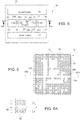
- Figure 5 shows an electronic device 50 comprising a printed-circuit board, PCB 52, carrying four MMICs, for example one Master MMIC 53 and three Slave MMICs 54-56 (even though the number of Slave MMICs may be different).
- the MMICs 53-56 are arranged side-by-side, between a receiving antenna structure (RX antenna 60, at the top in Figure 5 ) and a transmitting antenna structure (TX antenna 61, at the bottom in Figure 5 ).
- the MMICs 53-56 comprise a packaged electronic device 57, hereinafter also called die 57.
- the die 57 houses, in an own active area 57A, electronic components (represented schematically and designated as a whole by 58).
- a connection region 59 extends over the die 57 and forms an interface between the packaged electronic device 57 and the PCB 52.
- the connection region is formed by a dielectric layer accommodating metal connection lines 62, as described above with reference to Figure 4 .
- the connection region 59 is formed by a bonding support similar to the bonding support 7 of Figure 3 .
- the MMICs 53-56 are connected to the RX antenna 60 and the TX antenna 61 through surface electrical connections 63, formed as conductive tracks on the surface of the PCB 52 that carries the MMICs 53-56, in a known way.
- the MMICs 53-56 are mutually connected through buried connections, formed in the PCB 52, as described hereinafter, as well as through a synchronization line 64, described in detail hereinafter, which routes a synchronization signal LO, generated by the Master MMIC 53, through the electronic components 74 and supplied to the Slave MMICs 54-56 for their synchronization and amplitude balancing, in a per se known manner.
- the Slave MMICs 54-56 are also referred to as first, second, and third Slave MMICs 54, 55, and 56.
- the Master MMIC 53 is arranged between the first Slave MMIC 54 (located to the left) and the second Slave MMIC 55 (located to the right). Consequently, the synchronization signal LO crosses the Master MMIC 53 and the second Slave MMIC 55.
- the MMICs 53-56 (see also Figures 6 and 7 ) are fixed and electrically connected to the PCB 52 through the solder ball technique, which uses solder balls 65.
- the solder balls 65 may be bonded either using the FC-BGA technique or using the eWLB technique described above and shown in Figures 3 and 4 . It should be noted that hereinafter the term "balls" will be used, even though, after bonding, in general they are deformed and have a shape different from the spherical one.
- the solder balls 65 are coupled to the electronic components 58 by the metal connection lines 62 and extend on the whole area of the connection region 59 and, in particular, over the active area 57A accommodating the electronic components 58.
- solder balls 65 are arranged in rows and columns, identified in Figure 6 by the letters A-Y and the numbers 1-18, respectively, but on the row J no solder balls 65 are present.
- the row J defines an empty or missing row, i.e., the solder balls 65 arranged on the adjacent rows (rows K and H in Figure 6 ) are arranged at a distance from each other greater than the distance between the other adjacent rows.
- p denotes the pitch between adjacent rows in the array (i.e., the distance between the central points of solder balls 65 belonging to mutually adjacent rows)
- the synchronization line 64 extends (on the PCB 52) in the empty row, between two rows of solder balls 65 arranged at the distance d.
- the PCB 52 comprises, in a known way, a body 67 of dielectric material, which has a first face 67A and a second face 67B and embeds conductive regions 68 connected together and to the first face 67A through metal vias 69 for electrical connection between the MMICs 53-56.
- Possible vias may connect the conductive regions 68 also to the second face 67B of the PCB 52.
- the first face 67A of the PCB 52 moreover carries the surface electrical connections 63 (here not visible) and the synchronization line 64.
- the synchronization line 64 is here formed by a synchronization track 66 comprising a rectilinear portion 66A and branching portions 66B extending from the rectilinear portion 66A as far as respective solder balls 65 arranged at the terminals of the MMICs 53-56 intended to receive/emit the synchronization signal LO (denoted in Figure 5 by LOin for the input terminals and by LOout for the output terminals).
- the branching portions 66B connecting to the solder ball 65A coupled to the input terminal LOin and to the output terminal LOout of the Master MMIC 53 of Figure 5 are represented by dashed lines in Figure 6 .
- the rectilinear portion 66A of the synchronization line 64 extends only underneath the Master MMIC 53 and the second Slave MMIC 85, even though all the MMICs 53-56 have the empty row, and the branching portions 66B are connected to two solder balls 65 (solder balls 65A and 65B in Figure 6 ) for the Master MMIC 53 and to a single solder ball 65 for the MMICs 54-56.
- the rectilinear portion 66A is not necessarily formed by a single segment that traverses the Master MMIC 53 and the second Slave MMIC 85, but may be formed by a broken line, only the portions thereof crossing the single MMICs 53 and 55 being preferably linear.
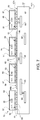
- the synchronization track 66 may be formed in the same way as the surface electrical connections 63 formed on the first face 67A of the PCB 52, for example as a copper track, and typically has a much lower thickness than the solder balls 65, even when these are slightly deformed after soldering, as visible in Figure 7 .
- Figures 8-10 show an electronic device 70 implementing a different solution for routing the synchronization signal LO.
- the MMICs comprise a microstrip (having a grounded region arranged underneath) or a coplanar waveguide (having grounded regions in the same plane as the waveguide).
- the microstrip or coplanar waveguide is formed above the dice, and extends practically throughout the width of each MMIC to connect opposite sides thereof. Connection with the terminals LOin and LOout is obtained through conductive tracks formed on the PCB and connected to the microstrip or coplanar waveguide through solder balls.
- This solution shown in Figures 8 and 9 as regards bonding of the MMICs through the eWLB technique, may be used also in case of bonding of the MMICs with the FC-BGA technique, as discussed below.
- the MMICs (here designated by 83-86) have a coupling face 81, are formed as shown in Figure 4 , and each comprise a die 73 integrating electronic components (designated as a whole by 74), a peripheral region 76, and a dielectric layer 72.
- Metal connection lines 75 represented schematically, extend in the dielectric layer 72 and are connected with solder balls 95, as described above with reference to Figure 4 .
- the Slave MMICs 84-86 are referred to as first, second, and third Slave MMICs.
- each die 73 derives from dicing a processed semiconductor wafer and comprises a semiconductor substrate (not shown) overlaid by one or more insulating layers (not shown) accommodating metal connection lines (not shown either), in a per se known manner.
- the MMICs 83-86 are arranged side-by-side, between a receiving antenna structure, RX antenna 90, and a transmitting antenna structure, TX antenna 91, and are coupled to the RX antenna 90 and TX antenna 91 through surface electrical connections 93 formed on the PCB (designated by 92) comprising, in a known way, a body 97 of dielectric material embedding conductive regions 98 connected together and to the first face 97A through metal vias 99.
- each MMIC 83-86 has a conductive strip 71 formed in the dielectric layer 72 of the Master MMIC 83 and of the Slave MMICs 84-86.
- the conductive strips 71 are here formed using a redistribution layer RDL.
- Figure 10 shows a variant of Figure 9 , where the MMICs 83-86 are bonded using the FC-BGA technique.
- the electronic device designated by 70', has conductive strips 71' formed in a metal layer similar to the ones used for forming metal connection lines 88, similar to the metal connection lines 18 of Figure 3 , within a connection substrate 89, similar to the connection substrate 7 of Figure 3 .
- the plates 8 are not shown, and the underfill layer, the bumps, and the caps are designated, respectively, by 77, 79, and 80.
- the conductive strips 71, 71' extend approximately throughout the width of the MMICs 83-86 (and thus of the dielectric layer 72 or of the connection substrate 89), ending only at a short distance from the edge thereof.
- width of the MMICs 53-56 indicates the size in the adjacency direction of the MMICs 53-56.
- the electronic device 70, 70' has a synchronization line 96 formed by the conductive strips 71, 71' of some of the MMICs 83-86 (the ones crossed by the synchronization line 96) and track portions 94 formed on the PCB 92.
- the conductive strips 71, 71' and the track portions 94 forming the synchronization line 96 are connected together by the solder balls 95.
- the synchronization line 96 is here formed by the conductive strips 71, 71' of the Master MMIC 83 and of the second Slave MMIC 85 (arranged in Figures 9 and 10 to the right of the Master MMIC 83).
- the conductive strips 71, 71' are not electrically coupled to any of the components 74 and are connected to the respective solder balls 95 of only the Master MMIC 83 and the second Slave MMIC 85.
- the conductive strips 71, 71' of the first Slave MMIC 84 (located furthest to the left in Figure 8 and partially visible in Figures 9 and 10 ) and of the third Slave MMIC 56 (located furthest to the right in Figure 8 and not visible in Figures 9 and 10 ) are floating (or connected to an appropriate fixed potential, for example ground).
- the conductive strips 71, 71' of the first Slave MMIC 84 and of the third Slave MMIC 56 may be connected to respective solder balls 95, but these are not connected to any metal line, or are possibly connected only to a common ground line, if envisaged.
- the track portions 94 formed on the PCB 92 enable connection of the synchronization line 96 to the input terminals LOin of the MMICs 83-86 and to the output terminal LOout of the Master MMIC 83.
- the solder ball coupled in a not shown way to the input terminal LOin of the first Slave MMIC 84 (represented dashed in Figures 9 and 10 in so far as it is not crossed by the section plane); by 95B the solder ball coupled to a first end (on the left in Figures 9 and 10 ) of the conductive strip 71, 71' of the Master MMIC 83; by 95C the solder ball coupled to a second end (on the right in Figures 9 and 10 ) of the conductive strip 71, 71' of the Master MMIC 83; and by 95D the solder ball coupled to a first end (on the left in Figures 9 and 10 ) of the conductive strip 71, 71' of the second S
- Figures 11-13 show an electronic device 100 implementing a different solution for routing the synchronization signal LO.
- the MMICs have a microstrip or a coplanar waveguide integrated within the die, and the microstrip or coplanar waveguide extends throughout the width of each die to connect opposite sides thereof. Connection with the terminals LOin and LOout takes place through metal connection lines or wires internal to the MMICs and conductive tracks formed on the PCB.
- This solution shown in Figures 11 and 12 as regards bonding the MMICs 83-86 through the eWLB technique, can be used also in the case of coupling of the MMICs 83-86 with the FC-BGA technique or with the wire-bonding technique, as discussed hereinafter with reference to Figure 13 .
- each MMIC 83-86 has a conductive strip 101 of metal, here formed by a metallization layer extending within the insulating layer 105 of each die 73.
- Each conductive strip 101 is here formed directly underneath a surface 73A of the respective die 73.
- each conductive strip 101 is connected at its own ends to respective solder balls 95 arranged on the edges of each MMIC 83, 85, by vias and contact pads 103 formed in the insulating layer 105, and respective metal connection lines 102 formed in the dielectric layer 72 and similar to the metal connection lines 71.
- the conductive strips 101 are not electrically connected to the electronic components 74 of the electronic device 100, as discussed above for the conductive strips 71, 71'.
- the conductive strips 101 forming the microstrips or coplanar waveguides are manufactured at wafer level, together with the components 74, and are already present when the wafer is diced to the individual dice 73.
- This solution may moreover be applied both in case of bonding using the FC-BGA bonding technique (in which case, the conductive strips 101 are electrically coupled to the solder balls 95 through bumps and a bonding support as shown in Figure 10 ) and to electronic devices configured to work at low frequency and provided with packages coupled to a PCB by wire bonding (wire-bonding packages).
- Figure 13 shows an electronic device 110 having the connection scheme of Figure 11 , but where the MMICs are connected through wire bonding. Consequently, same parts with the electronic device 100 of Figures 11 and 12 are designated by the same reference numbers and are not described any further.
- each MMIC 83-86 comprises bonding wires 115 connecting respective contact pads 103 to pins 116.
- the contact pads 103 are arranged at opposite ends of the conductive strips 101; each conductive strip 101 is formed within the insulation layer 105 of each die 73 and extends practically throughout the width thereof.
- the insulation layer 105 is shown as a single layer covering the semiconductor substrate 104 of each die 72 and open only at the contact pads 103.
- the insulation layer 105 may be formed by different layers arranged on top of each other, in a known way.
- the dice 73 and the bonding wires 115 are covered by a packaging layer 117 or a layer containing dielectric material, for example moulded resin (but the packaging layer may be formed according to any known packaging technique, as obvious to the person skilled in the art).
- the packaging layer 117 embeds also the pins 116 on all sides, except for the backside, where they are in direct electrical contact with the track portions 94 of the synchronization line 96.
- Figure 13 only the conductive strips 101 of the Master MMIC 83 and of the second Slave MMIC 85 are connected through the bonding wires 115. Consequently, the conductive strips 101 of the first and third MMICs 84, 86 are floating (or connected to an appropriate fixed potential, for example ground).
- Figure 13 thus shows with a dashed line (in so far as arranged in a parallel plane to the section plane) the bonding wire 115 connecting the input terminal LOin of the first Slave MMIC 84 to the first track portion 94A that is in electrical connection with an end of the conductive strip 101 of the Master MMIC 83, as explained above with reference to Figure 11 .
- the MMICs and the electronic device described herein have numerous advantages.
- the described solution allows the synchronization signal generated by the Master MMIC to be carried to the Slave MMICs without requiring an additional connection level in the PCB scheme, and thus at low costs.
- the described packaging structure allows the synchronization signal LO to be carried using (at least in part) the same conduction layer of the radiofrequency signals exchanged with the antenna structures 60, 61, 90, 91.
- the path of the synchronization signal LO is simplified and may be minimal, thus reducing loss phenomena or layout complexity.
- the MMICs may be arranged also not aligned to each other, but simply arranged side-by-side between the RX and TX antenna structures.
- the synchronization track 70 may comprise a broken line.
- the electronic device may comprise integrated circuits of a different type, even operating at different frequencies from radiofrequencies.
Landscapes
- Combinations Of Printed Boards (AREA)
- Physics & Mathematics (AREA)
- Geometry (AREA)
- Wire Bonding (AREA)
Abstract
Description
- The present invention relates to an integrated circuit and to an electronic device comprising a plurality of integrated circuits electrically coupled through a synchronization signal.
- In particular, electronic devices of this type are used in radiofrequency applications, for example in radars for use in motor vehicles (typically, in the 76 to 81 GHz frequency range), where a number of transmission and/or receiving channels are present, and/or in imaging applications, for example for medical use.
- In these types of multiple-channel applications, currently MMICs (Monolithic Microwave Integrated Circuits) are increasingly used by virtue of their uniform electrical characteristics (typically, they are matched to an impedance of 50 Ω), which cause them to be simple to use, as they may be easily cascade-connected without any need for external impedance-matching networks.
- In this way, it is possible to manufacture devices formed by a plurality of cascade-connected MMICs, each whereof is configured to manage a small number of transmitting/receiving channels. For instance, the MMICs may be connected together so that a first MMIC (referred to as Master) generates synchronization signals and supplies these signals to all the other MMICs (referred to as Slaves) . In particular, the Master generates a synchronization signal LO, at more or less high frequencies, according to the application (for example, at 20, 40, or 80 GHz). With this arrangement, all the MMICs receive the synchronization signal LO from the Master and are able to transmit and receive radiofrequency signals in a synchronized way, using transmitting and receiving antenna connections.
- For instance, in this way, a high end radar device is able to manage twelve receiving channels (hereinafter referred to as "RX channels") and nine transmitting channels (hereinafter referred to as "TX channels"), using three MMICs (one Master and two Slaves) that are each able to manage four RX channels and three TX channels. In more general terms, a radar device of this type is able to manage X RX channels and Y TX channels, using M MMICs that are each able to manage X/M RX channels and Y/M TX channels.
- In general, moreover, a MMIC-based device for transmitting/receiving radiofrequency signals comprises a printed-circuit board (PCB) carrying the MMICs and the antennas, and may have a layout of the type shown in
Figure 1 and described hereinafter. - For instance,
Figure 1 shows adevice 1 comprising a printed-circuit board (PCB 2) carrying one Master MMIC 3 and three Slave MMICs 4-6 (even though the number of MMICs may be greater or smaller) . In the top plan view ofFigure 1 , the MMICs 3-6 are set side-by-side, between a receiving antenna structure (RX antenna 10, at the top inFigure 1 ) and a transmitting antenna structure (TX antenna 11, at the bottom inFigure 1 ). - The high-frequency MMICs 3-6 are generally fixed to the
PCB 2 and electrically connected together through solder ball connections, as described in greater detail hereinafter. ThePCB 2 has surfaceelectrical connections 13, generally formed as conductive tracks on the surface of thePCB 2, for electrical connection of the MMICs 3-6 to theRX antenna 10 and theTX antenna 11; buriedelectrical connections 14, formed by conductive tracks generally extending in internal layers of thePCB 2; and connection vias, for connecting the different levels and the surface of thePCB 2, for exchanging signals and electrical quantities between the MMICs 3-6, in a known manner and shown only schematically inFigure 1 . - In radiofrequency applications, due to the high working frequency (generally, higher than 40 GHz), the solder ball connections are currently implemented through a FC-BGA (Flip Chip-Ball Grid Array) technique or an eWLB (embedded Wafer-Level BGA) technique.
- As is known, both techniques use ball-
grid arrays 15 fixed on one side, for example on the backside, of each MMIC 3-6 to be coupled to thePCB 2, as exemplary shown inFigure 2 , where the solder balls are designated by 15 and the generic MMIC is designated by 16. - In case of the FC-BGA technique (see
Figure 3 , which is a cross-section through a generic MMIC 16), thesolder balls 15 are fixed to one side of aconnection substrate 7 formed by twoplates 8 housingdielectric material 9. Thedielectric material 9 embedsmetal connection lines 18, which electrically connect thesolder balls 15 withbumps 17 fixed to theconnection substrate 7 on the side opposite to thesolder balls 15. Furthermore, thebumps 17 are fixed to a die 21 housing electronic components (designated as a whole by 22) and enable passage of signals and possible other electrical quantities (for example, supply quantities, hereinafter included in the term "signals") between theelectronic components 22 of each MMIC 3-6 and theconnection substrate 7. A dielectric filling and matching layer (so-called underfill layer 19) extends between the die 21 and theconnection substrate 7 and covers thebumps 17. Acap 12 is bonded to theconnection substrate 7 through anadhesive layer 23 and surrounds thedie 21, thebumps 17, and theunderfill layer 19, to form a sort of package with theconnection substrate 7. -
US 8,949,606 discloses a semiconductor device of the type shown infigure 3 . Here, a pellet is arranged on the upper surface of the substrate and is connected thereto by a plurality of terminals formed as solder bumps. The solder bumps are arranged to define a plurality of annular lines in the periphery of the pellet. A thin resin layer extend between the pellet and the substrate, in the space between the terminals, - In case of the eWLB technique (see
Figure 4 showing a cross-section through a portion of the generic MMIC 16), eachsolder ball 15 is generally fixed to a respectiveconductive region 25. The conductive regions 25 (just one whereof is shown) are made generally of copper within adielectric layer 26 and form one or more redistribution layers (inFigure 4 , a single redistribution layer RDL 24). Thedielectric layer 26 extends over apassivation layer 27 that covers a die 28 except for openings at thecontact pads 30 formed on the surface of the die 28 and electrically connected to electronic components (designated as a whole by 31) integrated in the die 28. Here, the die 28 is surrounded by aperipheral region 29. Theperipheral region 29 is generally manufactured by compression moulding and widens the area of the die 28, so that the dielectric layer 26 (which also extends over the peripheral region 29) nay have an greater area than the die 28, enabling thesolder balls 15 to be arranged over an area wider than the die 28, for example at a pitch of 500 µm. - The eWLB technique allows to obtain the minimum length of the interconnections and a very good electrical behaviour up to high frequencies (with a wavelength in the field of millimetres), does not require underlying filling with underfill material, makes it possible to have numerous input/output connections, and has a low cost.
- Among the signals exchanged between the MMICs 3-6, of particular importance is the synchronization signal LO, since it makes it possible to maintain phase coherence and amplification balancing between the MMICs 3-6.
- Currently, the synchronization signal LO (having two different inputs to enable a symmetrical routing in the PCB 2) is routed through the buried
connections 14 using an internal additional layer of thePCB 2, since these synchronization connections cannot be formed on the top layer of thePCB 2 in order not to cross the surfaceelectrical connections 13 with theRX antenna 10 and the TX antenna 11 (Figure 1 ). - This, however, entails an increase in the complexity of the buried
connections 14 and high costs for forming the internal additional layer of thePCB 2. Furthermore, transitions between the various layers increase, which leads to undesirable drops in signal amplitudes. - The aim of the present invention is to provide an integrated circuit and an electronic device that overcomes the drawbacks of the prior art, using the current connection techniques, for example the ones based upon solder balls.
- According to the present invention an integrated circuit and an electronic device are provided, as defined in the attached claims.
- For a better understanding of the present invention, some embodiments thereof are now described, purely by way of non-limiting example, with reference to the attached drawings, wherein:
-
Figure 1 shows the layout of an electronic device having a plurality of integrated circuits for radiofrequency applications of a known type; -
Figure 2 is a bottom perspective view of an integrated circuit configured to be bonded using the ball-grid-array technique; -
Figure 3 is a cross-section of a portion of the integrated circuit ofFigure 2 , configured to be bonded using the FC-BGA technique; -
Figure 4 is a cross-section of a portion of the integrated circuit ofFigure 2 , configured to be bonded using the eWLB technique; -
Figure 5 shows the layout of an electronic device having a plurality of integrated circuits, according to an embodiment; -
Figure 6 is a bottom view of the integrated circuit ofFigure 5 ; -
Figure 6A shows an enlarged detail of the integrated circuit ofFigure 6 ; -
Figure 7 is a cross-section of a portion of the integrated circuit ofFigure 5 ; -
Figure 8 shows the layout an electronic device having a plurality of integrated circuits according to another embodiment; -
Figure 9 is a cross-section of a portion of an integrated circuit of the electronic device ofFigure 8 , taken along section line IX-IX; -
Figure 10 is a different embodiment of the integrated circuit ofFigure 9 , taken along the same section line asFigure 9 ; -
Figure 11 shows the layout of an electronic device having a plurality of integrated circuits according to a different embodiment; -
Figure 12 is a cross-section of a portion of an integrated circuit of the electronic device ofFigure 11 , taken along section line XII-XII; and -
Figure 13 is a cross-section of a different embodiment of the integrated circuit ofFigure 12 , taken along the same section line asFigure 12 . -
Figure 5 shows anelectronic device 50 comprising a printed-circuit board,PCB 52, carrying four MMICs, for example one Master MMIC 53 and three Slave MMICs 54-56 (even though the number of Slave MMICs may be different). In the top plan view ofFigure 5 , the MMICs 53-56 are arranged side-by-side, between a receiving antenna structure (RX antenna 60, at the top inFigure 5 ) and a transmitting antenna structure (TX antenna 61, at the bottom inFigure 5 ). - With reference to
Figure 7 , the MMICs 53-56 comprise a packagedelectronic device 57, hereinafter also called die 57. The die 57 houses, in an ownactive area 57A, electronic components (represented schematically and designated as a whole by 58). Aconnection region 59 extends over the die 57 and forms an interface between the packagedelectronic device 57 and thePCB 52. In case of the eWLB bonding technique, the connection region is formed by a dielectric layer accommodatingmetal connection lines 62, as described above with reference toFigure 4 . In case of the FC-BGA bonding technique, theconnection region 59 is formed by a bonding support similar to thebonding support 7 ofFigure 3 . Not visible inFigure 7 are possible passivation layers, nor a possible peripheral region surrounding thedie 57, in case of the eWLB bonding technique, or the underfill layer and bumps, in case of the FC-BGA bonding technique, but they may be present, as shown inFigures 4 and 3 , respectively. - With reference once again to
Figure 5 , the MMICs 53-56 are connected to theRX antenna 60 and theTX antenna 61 through surfaceelectrical connections 63, formed as conductive tracks on the surface of thePCB 52 that carries the MMICs 53-56, in a known way. In addition, the MMICs 53-56 are mutually connected through buried connections, formed in thePCB 52, as described hereinafter, as well as through asynchronization line 64, described in detail hereinafter, which routes a synchronization signal LO, generated by the Master MMIC 53, through theelectronic components 74 and supplied to the Slave MMICs 54-56 for their synchronization and amplitude balancing, in a per se known manner. - Hereinafter, to enable better understanding, the Slave MMICs 54-56 are also referred to as first, second, and third Slave MMICs 54, 55, and 56. In the embodiment shown (see, in particular,
Figure 5 ), the Master MMIC 53 is arranged between the first Slave MMIC 54 (located to the left) and the second Slave MMIC 55 (located to the right). Consequently, the synchronization signal LO crosses the Master MMIC 53 and the second Slave MMIC 55. - The MMICs 53-56 (see also
Figures 6 and7 ) are fixed and electrically connected to thePCB 52 through the solder ball technique, which usessolder balls 65. Thesolder balls 65 may be bonded either using the FC-BGA technique or using the eWLB technique described above and shown inFigures 3 and 4 . It should be noted that hereinafter the term "balls" will be used, even though, after bonding, in general they are deformed and have a shape different from the spherical one. - The
solder balls 65 are coupled to theelectronic components 58 by themetal connection lines 62 and extend on the whole area of theconnection region 59 and, in particular, over theactive area 57A accommodating theelectronic components 58. - As may be noted in
Figure 6 , thesolder balls 65 are arranged in rows and columns, identified inFigure 6 by the letters A-Y and the numbers 1-18, respectively, but on the row J nosolder balls 65 are present. - In this way, the row J defines an empty or missing row, i.e., the
solder balls 65 arranged on the adjacent rows (rows K and H inFigure 6 ) are arranged at a distance from each other greater than the distance between the other adjacent rows. In particular, with reference to the enlarged detail ofFigure 6A , if p denotes the pitch between adjacent rows in the array (i.e., the distance between the central points ofsolder balls 65 belonging to mutually adjacent rows), at the empty row the distance d is twice the pitch p (d = 2p). - As represented by a dashed line in
Figure 6 , thesynchronization line 64 extends (on the PCB 52) in the empty row, between two rows ofsolder balls 65 arranged at the distance d. - With reference to
Figure 7 , thePCB 52 comprises, in a known way, abody 67 of dielectric material, which has afirst face 67A and asecond face 67B and embedsconductive regions 68 connected together and to thefirst face 67A throughmetal vias 69 for electrical connection between the MMICs 53-56. Possible vias (not shown) may connect theconductive regions 68 also to thesecond face 67B of thePCB 52. Thefirst face 67A of thePCB 52 moreover carries the surface electrical connections 63 (here not visible) and thesynchronization line 64. - In particular (see also
Figure 5 ), thesynchronization line 64 is here formed by asynchronization track 66 comprising arectilinear portion 66A and branchingportions 66B extending from therectilinear portion 66A as far asrespective solder balls 65 arranged at the terminals of the MMICs 53-56 intended to receive/emit the synchronization signal LO (denoted inFigure 5 by LOin for the input terminals and by LOout for the output terminals). For instance, the branchingportions 66B connecting to thesolder ball 65A coupled to the input terminal LOin and to the output terminal LOout of theMaster MMIC 53 ofFigure 5 are represented by dashed lines inFigure 6 . - In practice, in the embodiment shown in
Figure 5 , therectilinear portion 66A of thesynchronization line 64 extends only underneath theMaster MMIC 53 and thesecond Slave MMIC 85, even though all the MMICs 53-56 have the empty row, and the branchingportions 66B are connected to two solder balls 65 (solder balls Figure 6 ) for theMaster MMIC 53 and to asingle solder ball 65 for the MMICs 54-56. - However, the
rectilinear portion 66A is not necessarily formed by a single segment that traverses theMaster MMIC 53 and thesecond Slave MMIC 85, but may be formed by a broken line, only the portions thereof crossing thesingle MMICs - The
synchronization track 66 may be formed in the same way as the surfaceelectrical connections 63 formed on thefirst face 67A of thePCB 52, for example as a copper track, and typically has a much lower thickness than thesolder balls 65, even when these are slightly deformed after soldering, as visible inFigure 7 . -
Figures 8-10 show anelectronic device 70 implementing a different solution for routing the synchronization signal LO. Here, the MMICs comprise a microstrip (having a grounded region arranged underneath) or a coplanar waveguide (having grounded regions in the same plane as the waveguide). The microstrip or coplanar waveguide is formed above the dice, and extends practically throughout the width of each MMIC to connect opposite sides thereof. Connection with the terminals LOin and LOout is obtained through conductive tracks formed on the PCB and connected to the microstrip or coplanar waveguide through solder balls. This solution, shown inFigures 8 and 9 as regards bonding of the MMICs through the eWLB technique, may be used also in case of bonding of the MMICs with the FC-BGA technique, as discussed below. - In
Figures 8 and 9 , the MMICs (here designated by 83-86) have acoupling face 81, are formed as shown inFigure 4 , and each comprise a die 73 integrating electronic components (designated as a whole by 74), aperipheral region 76, and adielectric layer 72. Metal connection lines 75, represented schematically, extend in thedielectric layer 72 and are connected with solder balls 95, as described above with reference toFigure 4 . Furthermore, also here, for clarity, the Slave MMICs 84-86 are referred to as first, second, and third Slave MMICs. It should be noted that here, albeit not shown, each die 73 derives from dicing a processed semiconductor wafer and comprises a semiconductor substrate (not shown) overlaid by one or more insulating layers (not shown) accommodating metal connection lines (not shown either), in a per se known manner. - Furthermore, as in
Figure 5 , inFigure 8 , the MMICs 83-86 are arranged side-by-side, between a receiving antenna structure,RX antenna 90, and a transmitting antenna structure,TX antenna 91, and are coupled to theRX antenna 90 andTX antenna 91 through surfaceelectrical connections 93 formed on the PCB (designated by 92) comprising, in a known way, abody 97 of dielectric material embeddingconductive regions 98 connected together and to thefirst face 97A throughmetal vias 99. - Specifically, as regards the embodiment of
Figures 8 and 9 , each MMIC 83-86 has aconductive strip 71 formed in thedielectric layer 72 of theMaster MMIC 83 and of the Slave MMICs 84-86. - The
conductive strips 71 are here formed using a redistribution layer RDL. -
Figure 10 shows a variant ofFigure 9 , where the MMICs 83-86 are bonded using the FC-BGA technique. - Here, the electronic device, designated by 70', has conductive strips 71' formed in a metal layer similar to the ones used for forming
metal connection lines 88, similar to themetal connection lines 18 ofFigure 3 , within aconnection substrate 89, similar to theconnection substrate 7 ofFigure 3 . InFigure 10 theplates 8 are not shown, and the underfill layer, the bumps, and the caps are designated, respectively, by 77, 79, and 80. - In both cases of
Figures 9 and10 , theconductive strips 71, 71' extend approximately throughout the width of the MMICs 83-86 (and thus of thedielectric layer 72 or of the connection substrate 89), ending only at a short distance from the edge thereof. - It should be noted that, in this context, the term width of the MMICs 53-56 indicates the size in the adjacency direction of the MMICs 53-56.
- As shown in
Figure 8 , theelectronic device 70, 70' has asynchronization line 96 formed by theconductive strips 71, 71' of some of the MMICs 83-86 (the ones crossed by the synchronization line 96) andtrack portions 94 formed on thePCB 92. The conductive strips 71, 71' and thetrack portions 94 forming thesynchronization line 96 are connected together by the solder balls 95. - In detail, the
synchronization line 96 is here formed by theconductive strips 71, 71' of theMaster MMIC 83 and of the second Slave MMIC 85 (arranged inFigures 9 and10 to the right of the Master MMIC 83). The conductive strips 71, 71' are not electrically coupled to any of thecomponents 74 and are connected to the respective solder balls 95 of only theMaster MMIC 83 and thesecond Slave MMIC 85. Consequently, theconductive strips 71, 71' of the first Slave MMIC 84 (located furthest to the left inFigure 8 and partially visible inFigures 9 and10 ) and of the third Slave MMIC 56 (located furthest to the right inFigure 8 and not visible inFigures 9 and10 ) are floating (or connected to an appropriate fixed potential, for example ground). - As an alternative to the above, the
conductive strips 71, 71' of thefirst Slave MMIC 84 and of thethird Slave MMIC 56 may be connected to respective solder balls 95, but these are not connected to any metal line, or are possibly connected only to a common ground line, if envisaged. - The
track portions 94 formed on thePCB 92 enable connection of thesynchronization line 96 to the input terminals LOin of the MMICs 83-86 and to the output terminal LOout of theMaster MMIC 83. In detail, with reference toFigures 9 and10 , by identifying with 95A the solder ball coupled in a not shown way to the input terminal LOin of the first Slave MMIC 84 (represented dashed inFigures 9 and10 in so far as it is not crossed by the section plane); by 95B the solder ball coupled to a first end (on the left inFigures 9 and10 ) of the conductive strip 71, 71' of the Master MMIC 83; by 95C the solder ball coupled to a second end (on the right inFigures 9 and10 ) of the conductive strip 71, 71' of the Master MMIC 83; and by 95D the solder ball coupled to a first end (on the left inFigures 9 and10 ) of the conductive strip 71, 71' of the second Slave MMIC 85, a first track portion 94A connects the solder ball 95A of the Slave MMIC 85 to the solder ball 95B of the Master MMIC 83 and to a solder ball (not visible) coupled in a way not shown to the input terminal LOin of the Master MMIC 83; a second track portion 94B connects the solder ball 95C of the Master MMIC 53 to the solder ball 95D of the second Slave MMIC 85 and to a solder ball (not visible) coupled in a way not shown to the output terminal LOout of the Master MMIC 83; a third track portion 94C (shown only inFigure 8 ) connects the second end of the conductive strip 71 of the second Slave MMIC 85 to solder balls (not visible) coupled to the input terminal LOin of the second Slave MMIC 85 and to the input terminal LOin of the third Slave MMIC 86. - It should be noted that this solution can be applied also in case of a wire-bonding/solder ball mixed technique, as evident to the person skilled in the art.
-
Figures 11-13 show anelectronic device 100 implementing a different solution for routing the synchronization signal LO. Here, the MMICs have a microstrip or a coplanar waveguide integrated within the die, and the microstrip or coplanar waveguide extends throughout the width of each die to connect opposite sides thereof. Connection with the terminals LOin and LOout takes place through metal connection lines or wires internal to the MMICs and conductive tracks formed on the PCB. This solution, shown inFigures 11 and 12 as regards bonding the MMICs 83-86 through the eWLB technique, can be used also in the case of coupling of the MMICs 83-86 with the FC-BGA technique or with the wire-bonding technique, as discussed hereinafter with reference toFigure 13 . - In detail, as shown in
Figures 11 and 12 , where same parts of theelectronic device 70 ofFigures 8 and 9 are designated by the same reference numbers and are not described any further, and thedice 73 are represented as formed by asemiconductor substrate 104 overlaid by aninsulation layer 105, each MMIC 83-86 has aconductive strip 101 of metal, here formed by a metallization layer extending within the insulatinglayer 105 of each die 73. Eachconductive strip 101 is here formed directly underneath asurface 73A of therespective die 73. In case of theMaster MMIC 83 and of thesecond Slave MMIC 85, eachconductive strip 101 is connected at its own ends to respective solder balls 95 arranged on the edges of eachMMIC contact pads 103 formed in the insulatinglayer 105, and respectivemetal connection lines 102 formed in thedielectric layer 72 and similar to the metal connection lines 71. In case of the first andthird Slave MMICs conductive strips 101 are not electrically connected to theelectronic components 74 of theelectronic device 100, as discussed above for theconductive strips 71, 71'. - In practice, in this case, the
conductive strips 101 forming the microstrips or coplanar waveguides are manufactured at wafer level, together with thecomponents 74, and are already present when the wafer is diced to theindividual dice 73. - This solution may moreover be applied both in case of bonding using the FC-BGA bonding technique (in which case, the
conductive strips 101 are electrically coupled to the solder balls 95 through bumps and a bonding support as shown inFigure 10 ) and to electronic devices configured to work at low frequency and provided with packages coupled to a PCB by wire bonding (wire-bonding packages). - For instance,
Figure 13 shows anelectronic device 110 having the connection scheme ofFigure 11 , but where the MMICs are connected through wire bonding. Consequently, same parts with theelectronic device 100 ofFigures 11 and 12 are designated by the same reference numbers and are not described any further. - In particular, in the example shown in
Figure 13 , each MMIC 83-86 comprisesbonding wires 115 connectingrespective contact pads 103 topins 116. Also here, thecontact pads 103 are arranged at opposite ends of theconductive strips 101; eachconductive strip 101 is formed within theinsulation layer 105 of each die 73 and extends practically throughout the width thereof. InFigure 13 , for simplicity, theinsulation layer 105 is shown as a single layer covering thesemiconductor substrate 104 of each die 72 and open only at thecontact pads 103. However, theinsulation layer 105 may be formed by different layers arranged on top of each other, in a known way. - The
dice 73 and thebonding wires 115 are covered by apackaging layer 117 or a layer containing dielectric material, for example moulded resin (but the packaging layer may be formed according to any known packaging technique, as obvious to the person skilled in the art). Thepackaging layer 117 embeds also thepins 116 on all sides, except for the backside, where they are in direct electrical contact with thetrack portions 94 of thesynchronization line 96. - As in
Figure 12 , inFigure 13 only theconductive strips 101 of theMaster MMIC 83 and of thesecond Slave MMIC 85 are connected through thebonding wires 115. Consequently, theconductive strips 101 of the first andthird MMICs Figure 13 thus shows with a dashed line (in so far as arranged in a parallel plane to the section plane) thebonding wire 115 connecting the input terminal LOin of thefirst Slave MMIC 84 to thefirst track portion 94A that is in electrical connection with an end of theconductive strip 101 of theMaster MMIC 83, as explained above with reference toFigure 11 . - The MMICs and the electronic device described herein have numerous advantages.
- In particular, the described solution allows the synchronization signal generated by the Master MMIC to be carried to the Slave MMICs without requiring an additional connection level in the PCB scheme, and thus at low costs.
- The described packaging structure allows the synchronization signal LO to be carried using (at least in part) the same conduction layer of the radiofrequency signals exchanged with the
antenna structures - The path of the synchronization signal LO is simplified and may be minimal, thus reducing loss phenomena or layout complexity.
- Finally, it is clear that modifications and variations may be made to the integrated circuit and to the electronic device described and shown herein, without thereby departing from the scope of the present invention, as defined in the attached claims. For instance, the described different embodiments may be combined so as to provide further solutions.
- For example, the MMICs may be arranged also not aligned to each other, but simply arranged side-by-side between the RX and TX antenna structures. In this case, the
synchronization track 70 may comprise a broken line. - The electronic device may comprise integrated circuits of a different type, even operating at different frequencies from radiofrequencies.
Claims (13)
- An integrated circuit (53-56), comprising:a die (57) including semiconductor material and integrating electronic components (58);a connection region (59) having a first and a second face, the connection region being coupled to the die with the first face and housing conductive connection lines (62);a plurality of solder balls (65), fixed to the connection region (59) and electrically coupled to the electronic components (58), the solder balls (65) being arranged in an array and being aligned along a plurality of lines parallel to a direction,wherein the plurality of lines comprises an empty line along which no solder balls are present.
- The integrated circuit according to claim 1, wherein the first lines are arranged at a mutually uniform, first distance (p) and first adjacent lines belonging to the plurality of lines and directly adjacent the empty line, are arranged at a mutual, second distance (d), the second distance being greater than the first distance.
- The integrated circuit according to claim 2, wherein the second distance (d) is twice the first distance (p).
- The integrated circuit according to any of the preceding claims, forming a Monolithic Microwave Integrated Circuit (MMIC).
- The integrated circuit according to any of the preceding claims, wherein the electronic components (58) are accommodated in an active area (57A) of the die (57) and the solder balls (65) extend vertically, at least in part, over the active area.
- An electronic device comprising:a support (52) having a face (67A);a plurality of integrated circuits (53-56) according to any of claims 1-5, the plurality of solder balls being fixed between the face (67A) of the support (52) and the respective integrated circuit (53-56);antenna structures (60, 61), formed on the face of the support;electric connection paths (63), formed on the face of the support and electrically coupling the antenna structures (60, 61) to first solder balls of the plurality of solder balls of each integrated circuit; anda conductive synchronization path (66) extending over the face (67A) of the support (52) and electrically coupled to at least a first solder ball (65A, 65B) of each integrated circuit, the conductive synchronization path (66) having at least a first portion (66A) extending along the empty line of at least one integrated circuit (53) of the plurality of integrated circuits (53-56).
- The electronic device according to the preceding claim, wherein the conductive synchronization path (66) is laterally surrounded by the solder balls (65) of the at least one integrated circuit (53) of the plurality of integrated circuits (53-56).
- The electronic device according to claim 6 or 7, wherein the connection region (59) forms an interface between the die (57) and the support (52) and the solder balls (65) are arranged between the connection region (59) and the support (52).
- The electronic device according to any of claims 6-8, wherein the support (52) is a PCB.
- The electronic device according to any of claims 6-9, wherein:the at least one integrated circuit (53) forms a master integrated circuit and comprises an output terminal (LOout) coupled to a second solder ball (65B) and configured to generate a synchronization signal,the plurality of integrated circuits (53-56) comprises a first and a second slave integrated circuit (54, 55), the first and the second slave integrated circuits being arranged on different sides of the master integrated circuit (53), andthe conductive synchronization path (66) furthermore has connection portions (66B) extending over the face (67A) of the support (52), branching off from the first portion (66A) and coupled to the first solder balls (65A, 65B) of the master integrated circuit (53) and of the first and second slave integrated circuits (54-56).
- The electronic device according to the preceding claim, wherein the connection portions (66B) comprise a first connection portion extending between the master integrated circuit (53) and the first slave integrated circuit (54), a second connection portion extending between the master integrated circuit (53) and the second slave integrated circuit (55), a third connection portion (66B) extending between the first portion (66A) and a respective first solder ball (65A) of the master integrated circuit (53), and a fourth connection portion (66B) extending between the second portion (66B) and the second solder ball (65B) of the master integrated circuit (53), the third and the fourth connection portions (66A, 66B) extending on opposite sides of the master integrated circuit (53).
- The electronic device according to any of claims 6-11, wherein the solder balls form a Flip-Chip Ball-Grid-Array coupling or an embedded Wafer-Level BGA coupling.
- The electronic device according to any of claims 6-12, constituting a microwave radar.
Applications Claiming Priority (1)
| Application Number | Priority Date | Filing Date | Title |
|---|---|---|---|
| IT102020000001819A IT202000001819A1 (en) | 2020-01-30 | 2020-01-30 | INTEGRATED CIRCUIT AND ELECTRONIC DEVICE INCLUDING A PLURALITY OF INTEGRATED CIRCUITS ELECTRICALLY COUPLED VIA A SYNCHRONIZATION SIGNAL |
Publications (2)
| Publication Number | Publication Date |
|---|---|
| EP3869541A2 true EP3869541A2 (en) | 2021-08-25 |
| EP3869541A3 EP3869541A3 (en) | 2021-12-08 |
Family
ID=70228713
Family Applications (1)
| Application Number | Title | Priority Date | Filing Date |
|---|---|---|---|
| EP21153537.2A Withdrawn EP3869541A3 (en) | 2020-01-30 | 2021-01-26 | Integrated circuit and electronic device comprising a plurality of integrated circuits electrically coupled through a synchronization signal |
Country Status (4)
| Country | Link |
|---|---|
| US (2) | US11742311B2 (en) |
| EP (1) | EP3869541A3 (en) |
| CN (2) | CN113206069B (en) |
| IT (1) | IT202000001819A1 (en) |
Families Citing this family (4)
| Publication number | Priority date | Publication date | Assignee | Title |
|---|---|---|---|---|
| IT202000001819A1 (en) * | 2020-01-30 | 2021-07-30 | St Microelectronics Srl | INTEGRATED CIRCUIT AND ELECTRONIC DEVICE INCLUDING A PLURALITY OF INTEGRATED CIRCUITS ELECTRICALLY COUPLED VIA A SYNCHRONIZATION SIGNAL |
| IT202000001822A1 (en) * | 2020-01-30 | 2021-07-30 | St Microelectronics Srl | INTEGRATED CIRCUIT AND ELECTRONIC DEVICE INCLUDING A PLURALITY OF INTEGRATED CIRCUITS ELECTRICALLY COUPLED VIA A SYNCHRONIZATION SIGNAL INSTRUCTED THROUGH THE INTEGRATED CIRCUIT |
| KR20250105015A (en) * | 2023-12-29 | 2025-07-08 | 삼성전자주식회사 | Radio module and electronic device including the same |
| CN118016638B (en) * | 2024-04-10 | 2024-07-12 | 成都天成电科科技有限公司 | Low-loss broadband transition structure suitable for wafer level packaging |
Citations (1)
| Publication number | Priority date | Publication date | Assignee | Title |
|---|---|---|---|---|
| US8949606B2 (en) | 2009-07-14 | 2015-02-03 | Audi Ag | Prevention of masquerade by using identification sequences |
Family Cites Families (48)
| Publication number | Priority date | Publication date | Assignee | Title |
|---|---|---|---|---|
| JP3534501B2 (en) * | 1995-08-25 | 2004-06-07 | 株式会社ルネサステクノロジ | Method for manufacturing semiconductor device |
| US6057600A (en) * | 1997-11-27 | 2000-05-02 | Kyocera Corporation | Structure for mounting a high-frequency package |
| US6180445B1 (en) * | 2000-04-24 | 2001-01-30 | Taiwan Semiconductor Manufacturing Company | Method to fabricate high Q inductor by redistribution layer when flip-chip package is employed |
| TWI245395B (en) * | 2001-11-20 | 2005-12-11 | Advanced Semiconductor Eng | Multi-chip module package device |
| US6770955B1 (en) | 2001-12-15 | 2004-08-03 | Skyworks Solutions, Inc. | Shielded antenna in a semiconductor package |
| JP3657246B2 (en) * | 2002-07-29 | 2005-06-08 | Necエレクトロニクス株式会社 | Semiconductor device |
| US20050002167A1 (en) * | 2003-07-02 | 2005-01-06 | John Hsuan | Microelectronic package |
| WO2007023327A1 (en) * | 2005-08-24 | 2007-03-01 | Infineon Technologies Ag | Magnetically alignable semiconductor chip and rewiring substrate and a method for magnetically aligning the semiconductor chip and the rewiring substrate |
| US20070141751A1 (en) * | 2005-12-16 | 2007-06-21 | Mistry Addi B | Stackable molded packages and methods of making the same |
| US7915081B2 (en) * | 2006-03-31 | 2011-03-29 | Intel Corporation | Flexible interconnect pattern on semiconductor package |
| US7741158B2 (en) | 2006-06-08 | 2010-06-22 | Unisem (Mauritius) Holdings Limited | Method of making thermally enhanced substrate-base package |
| US8860178B2 (en) * | 2006-07-03 | 2014-10-14 | Renesas Electronics Corporation | Semiconductor device having an inductor |
| JP5028968B2 (en) * | 2006-11-17 | 2012-09-19 | 日立電線株式会社 | Semiconductor device, stacked semiconductor device, and interposer substrate |
| JP5058714B2 (en) * | 2007-08-21 | 2012-10-24 | スパンション エルエルシー | Semiconductor device and manufacturing method thereof |
| US8278749B2 (en) * | 2009-01-30 | 2012-10-02 | Infineon Technologies Ag | Integrated antennas in wafer level package |
| US8358002B2 (en) * | 2009-12-23 | 2013-01-22 | Marvell World Trade Ltd. | Window ball grid array (BGA) semiconductor packages |
| US8451618B2 (en) * | 2010-10-28 | 2013-05-28 | Infineon Technologies Ag | Integrated antennas in wafer level package |
| KR101582395B1 (en) | 2011-03-24 | 2016-01-11 | 키사, 아이엔씨. | Integrated circuit with electromagnetic communication |
| JP5417389B2 (en) * | 2011-07-13 | 2014-02-12 | 株式会社東芝 | Wireless device |
| JP5839267B2 (en) * | 2011-09-28 | 2016-01-06 | 住友電工デバイス・イノベーション株式会社 | Manufacturing method of semiconductor device |
| US8648454B2 (en) | 2012-02-14 | 2014-02-11 | International Business Machines Corporation | Wafer-scale package structures with integrated antennas |
| US8786060B2 (en) * | 2012-05-04 | 2014-07-22 | Advanced Semiconductor Engineering, Inc. | Semiconductor package integrated with conformal shield and antenna |
| KR101963883B1 (en) * | 2012-07-05 | 2019-04-01 | 삼성전자주식회사 | Semiconductor package and method of forming the same |
| US8866292B2 (en) * | 2012-10-19 | 2014-10-21 | Infineon Technologies Ag | Semiconductor packages with integrated antenna and methods of forming thereof |
| US20140367854A1 (en) * | 2013-06-17 | 2014-12-18 | Broadcom Corporation | Interconnect structure for molded ic packages |
| JP6263948B2 (en) | 2013-10-17 | 2018-01-24 | 住友電気工業株式会社 | Electrode pad structure |
| KR102258101B1 (en) * | 2014-12-05 | 2021-05-28 | 삼성전자주식회사 | Package on package and mobile computing device having the same |
| US9537199B2 (en) * | 2015-03-19 | 2017-01-03 | International Business Machines Corporation | Package structure having an integrated waveguide configured to communicate between first and second integrated circuit chips |
| US10636753B2 (en) * | 2015-07-29 | 2020-04-28 | STATS ChipPAC Pte. Ltd. | Antenna in embedded wafer-level ball-grid array package |
| JP6350759B2 (en) | 2015-08-18 | 2018-07-04 | 三菱電機株式会社 | Semiconductor device |
| US9842820B1 (en) | 2015-12-04 | 2017-12-12 | Altera Corporation | Wafer-level fan-out wirebond packages |
| JP6643714B2 (en) | 2016-03-10 | 2020-02-12 | 富士通株式会社 | Electronic devices and equipment |
| US10128192B2 (en) | 2016-07-22 | 2018-11-13 | Mediatek Inc. | Fan-out package structure |
| CN107871732A (en) * | 2016-09-23 | 2018-04-03 | 深圳市中兴微电子技术有限公司 | Encapsulating structure |
| DE102017119212A1 (en) * | 2016-12-20 | 2018-06-21 | Infineon Technologies Ag | RF transceiver with test option |
| CN108695284A (en) * | 2017-04-07 | 2018-10-23 | 晟碟信息科技(上海)有限公司 | Include the semiconductor equipment of Top-down design semiconductor package body group |
| CN111033735B (en) * | 2017-09-04 | 2023-05-23 | 三菱电机株式会社 | Semiconductor module and power conversion device |
| DE102019106030A1 (en) * | 2018-03-22 | 2019-09-26 | Infineon Technologies Ag | RADAR SYSTEM WITH MULTIPLE RADAR CHIPS |
| US11302599B2 (en) * | 2018-04-19 | 2022-04-12 | Intel Corporation | Heat dissipation device having a thermally conductive structure and a thermal isolation structure in the thermally conductive structure |
| DE102018114471B4 (en) * | 2018-06-15 | 2020-02-06 | Infineon Technologies Ag | PHASE MEASUREMENT IN A RADAR SYSTEM |
| US11791312B2 (en) * | 2018-12-04 | 2023-10-17 | Qorvo Us, Inc. | MMICs with backside interconnects for fanout-style packaging |
| US11557545B2 (en) | 2018-12-04 | 2023-01-17 | Qorvo Us, Inc. | Monolithic microwave integrated circuit (MMIC) with embedded transmission line (ETL) ground shielding |
| US11626340B2 (en) * | 2019-12-12 | 2023-04-11 | Qorvo Us, Inc. | Integrated circuit (IC) package with embedded heat spreader in a redistribution layer (RDL) |
| US11296670B2 (en) | 2020-01-23 | 2022-04-05 | Qualcomm Incorporated | Impedance matching transceiver |
| IT202000001822A1 (en) | 2020-01-30 | 2021-07-30 | St Microelectronics Srl | INTEGRATED CIRCUIT AND ELECTRONIC DEVICE INCLUDING A PLURALITY OF INTEGRATED CIRCUITS ELECTRICALLY COUPLED VIA A SYNCHRONIZATION SIGNAL INSTRUCTED THROUGH THE INTEGRATED CIRCUIT |
| IT202000001819A1 (en) * | 2020-01-30 | 2021-07-30 | St Microelectronics Srl | INTEGRATED CIRCUIT AND ELECTRONIC DEVICE INCLUDING A PLURALITY OF INTEGRATED CIRCUITS ELECTRICALLY COUPLED VIA A SYNCHRONIZATION SIGNAL |
| EP4128534A1 (en) | 2020-04-03 | 2023-02-08 | Wolfspeed, Inc. | Stacked rf circuit topology using transistor die with through silicon carbide vias on gate and/or drain |
| WO2021202199A1 (en) | 2020-04-03 | 2021-10-07 | Cree, Inc. | Group iii nitride-based radio frequency amplifiers having back side source, gate and/or drain terminals |
-
2020
- 2020-01-30 IT IT102020000001819A patent/IT202000001819A1/en unknown
-
2021
- 2021-01-26 EP EP21153537.2A patent/EP3869541A3/en not_active Withdrawn
- 2021-01-29 US US17/162,595 patent/US11742311B2/en active Active
- 2021-02-01 CN CN202110139579.XA patent/CN113206069B/en active Active
- 2021-02-01 CN CN202120282004.9U patent/CN215600361U/en not_active Withdrawn - After Issue
-
2023
- 2023-06-13 US US18/334,280 patent/US12424578B2/en active Active
Patent Citations (1)
| Publication number | Priority date | Publication date | Assignee | Title |
|---|---|---|---|---|
| US8949606B2 (en) | 2009-07-14 | 2015-02-03 | Audi Ag | Prevention of masquerade by using identification sequences |
Also Published As
| Publication number | Publication date |
|---|---|
| US20230335524A1 (en) | 2023-10-19 |
| CN215600361U (en) | 2022-01-21 |
| CN113206069B (en) | 2025-12-19 |
| IT202000001819A1 (en) | 2021-07-30 |
| US12424578B2 (en) | 2025-09-23 |
| CN113206069A (en) | 2021-08-03 |
| US11742311B2 (en) | 2023-08-29 |
| US20210242157A1 (en) | 2021-08-05 |
| EP3869541A3 (en) | 2021-12-08 |
Similar Documents
| Publication | Publication Date | Title |
|---|---|---|
| US12424578B2 (en) | Integrated circuit and electronic device comprising a plurality of integrated circuits electrically coupled through a synchronization signal | |
| US11854954B2 (en) | Integrated circuit and electronic device comprising a plurality of integrated circuits electrically coupled through a synchronization signal routed through the integrated circuit | |
| KR101397748B1 (en) | Radio frequency(rf) integated circuit(ic) packages with integrated aperture-coupled patch antenna(s) | |
| CN112051551B (en) | Silicon-based three-dimensional integrated micro radar high-frequency high-power active sub-array | |
| US10103450B2 (en) | Integration of area efficient antennas for phased array or wafer scale array antenna applications | |
| US10038232B2 (en) | Semiconductor wafer including an integrated waveguide for communicating signals between first and second integrated circuit dies | |
| US6489676B2 (en) | Semiconductor device having an interconnecting post formed on an interposer within a sealing resin | |
| CN103247581B (en) | chip package and device | |
| EP3151276B1 (en) | Methods to improve bga package isolation in radio frequency and millimeter wave products | |
| US20100327068A1 (en) | Compact millimeter wave packages with integrated antennas | |
| KR20150002705A (en) | Redirection of electromagnetic signals using substrate structures | |
| KR20230038237A (en) | Quantum computing circuit including a plurality of chips and manufacturing method thereof | |
| US20160299361A1 (en) | High bandwidth rf or microwave interconnects for optical modulators | |
| EP1113497A2 (en) | Semiconductor package with conductor impedance selected during assembly | |
| CA3158060A1 (en) | Flip-chip ball grid array-type integrated circuit package for very high frequency operation | |
| EP4362219A1 (en) | Antenna structure and antenna structure manufacturing method | |
| JP2882396B2 (en) | Semiconductor device | |
| US20250349759A1 (en) | Launcher in package semiconductor device and assembly |
Legal Events
| Date | Code | Title | Description |
|---|---|---|---|
| PUAI | Public reference made under article 153(3) epc to a published international application that has entered the european phase |
Free format text: ORIGINAL CODE: 0009012 |
|
| STAA | Information on the status of an ep patent application or granted ep patent |
Free format text: STATUS: THE APPLICATION HAS BEEN PUBLISHED |
|
| AK | Designated contracting states |
Kind code of ref document: A2 Designated state(s): AL AT BE BG CH CY CZ DE DK EE ES FI FR GB GR HR HU IE IS IT LI LT LU LV MC MK MT NL NO PL PT RO RS SE SI SK SM TR |
|
| PUAL | Search report despatched |
Free format text: ORIGINAL CODE: 0009013 |
|
| AK | Designated contracting states |
Kind code of ref document: A3 Designated state(s): AL AT BE BG CH CY CZ DE DK EE ES FI FR GB GR HR HU IE IS IT LI LT LU LV MC MK MT NL NO PL PT RO RS SE SI SK SM TR |
|
| RIC1 | Information provided on ipc code assigned before grant |
Ipc: H01L 23/522 20060101ALI20211104BHEP Ipc: H01L 23/66 20060101ALI20211104BHEP Ipc: H01L 21/60 20060101AFI20211104BHEP |
|
| STAA | Information on the status of an ep patent application or granted ep patent |
Free format text: STATUS: REQUEST FOR EXAMINATION WAS MADE |
|
| 17P | Request for examination filed |
Effective date: 20220607 |
|
| RBV | Designated contracting states (corrected) |
Designated state(s): AL AT BE BG CH CY CZ DE DK EE ES FI FR GB GR HR HU IE IS IT LI LT LU LV MC MK MT NL NO PL PT RO RS SE SI SK SM TR |
|
| STAA | Information on the status of an ep patent application or granted ep patent |
Free format text: STATUS: EXAMINATION IS IN PROGRESS |
|
| 17Q | First examination report despatched |
Effective date: 20240119 |
|
| STAA | Information on the status of an ep patent application or granted ep patent |
Free format text: STATUS: THE APPLICATION HAS BEEN WITHDRAWN |
|
| 18W | Application withdrawn |
Effective date: 20260310 |