EP3869510A1 - Resistance reduction for word lines in memory arrays - Google Patents
Resistance reduction for word lines in memory arrays Download PDFInfo
- Publication number
- EP3869510A1 EP3869510A1 EP20208294.7A EP20208294A EP3869510A1 EP 3869510 A1 EP3869510 A1 EP 3869510A1 EP 20208294 A EP20208294 A EP 20208294A EP 3869510 A1 EP3869510 A1 EP 3869510A1
- Authority
- EP
- European Patent Office
- Prior art keywords
- word line
- resistivity
- memory array
- word lines
- word
- Prior art date
- Legal status (The legal status is an assumption and is not a legal conclusion. Google has not performed a legal analysis and makes no representation as to the accuracy of the status listed.)
- Granted
Links
Images




Classifications
-
- H—ELECTRICITY
- H10—SEMICONDUCTOR DEVICES; ELECTRIC SOLID-STATE DEVICES NOT OTHERWISE PROVIDED FOR
- H10B—ELECTRONIC MEMORY DEVICES
- H10B43/00—EEPROM devices comprising charge-trapping gate insulators
- H10B43/20—EEPROM devices comprising charge-trapping gate insulators characterised by three-dimensional [3D] arrangements, e.g. with cells on different height levels
- H10B43/23—EEPROM devices comprising charge-trapping gate insulators characterised by three-dimensional [3D] arrangements, e.g. with cells on different height levels with source and drain on different levels, e.g. with sloping channels
- H10B43/27—EEPROM devices comprising charge-trapping gate insulators characterised by three-dimensional [3D] arrangements, e.g. with cells on different height levels with source and drain on different levels, e.g. with sloping channels the channels comprising vertical portions, e.g. U-shaped channels
-
- H—ELECTRICITY
- H10—SEMICONDUCTOR DEVICES; ELECTRIC SOLID-STATE DEVICES NOT OTHERWISE PROVIDED FOR
- H10W—GENERIC PACKAGES, INTERCONNECTIONS, CONNECTORS OR OTHER CONSTRUCTIONAL DETAILS OF DEVICES COVERED BY CLASS H10
- H10W20/00—Interconnections in chips, wafers or substrates
- H10W20/40—Interconnections external to wafers or substrates, e.g. back-end-of-line [BEOL] metallisations or vias connecting to gate electrodes
- H10W20/41—Interconnections external to wafers or substrates, e.g. back-end-of-line [BEOL] metallisations or vias connecting to gate electrodes characterised by their conductive parts
- H10W20/44—Conductive materials thereof
- H10W20/4451—Semiconductor materials, e.g. polysilicon
-
- G—PHYSICS
- G11—INFORMATION STORAGE
- G11C—STATIC STORES
- G11C16/00—Erasable programmable read-only memories
- G11C16/02—Erasable programmable read-only memories electrically programmable
- G11C16/06—Auxiliary circuits, e.g. for writing into memory
- G11C16/08—Address circuits; Decoders; Word-line control circuits
-
- G—PHYSICS
- G11—INFORMATION STORAGE
- G11C—STATIC STORES
- G11C16/00—Erasable programmable read-only memories
- G11C16/02—Erasable programmable read-only memories electrically programmable
- G11C16/04—Erasable programmable read-only memories electrically programmable using variable threshold transistors, e.g. FAMOS
- G11C16/0483—Erasable programmable read-only memories electrically programmable using variable threshold transistors, e.g. FAMOS comprising cells having several storage transistors connected in series
-
- H—ELECTRICITY
- H10—SEMICONDUCTOR DEVICES; ELECTRIC SOLID-STATE DEVICES NOT OTHERWISE PROVIDED FOR
- H10B—ELECTRONIC MEMORY DEVICES
- H10B41/00—Electrically erasable-and-programmable ROM [EEPROM] devices comprising floating gates
- H10B41/10—Electrically erasable-and-programmable ROM [EEPROM] devices comprising floating gates characterised by the top-view layout
-
- H—ELECTRICITY
- H10—SEMICONDUCTOR DEVICES; ELECTRIC SOLID-STATE DEVICES NOT OTHERWISE PROVIDED FOR
- H10B—ELECTRONIC MEMORY DEVICES
- H10B41/00—Electrically erasable-and-programmable ROM [EEPROM] devices comprising floating gates
- H10B41/20—Electrically erasable-and-programmable ROM [EEPROM] devices comprising floating gates characterised by three-dimensional [3D] arrangements, e.g. with cells on different height levels
- H10B41/23—Electrically erasable-and-programmable ROM [EEPROM] devices comprising floating gates characterised by three-dimensional [3D] arrangements, e.g. with cells on different height levels with source and drain on different levels, e.g. with sloping channels
- H10B41/27—Electrically erasable-and-programmable ROM [EEPROM] devices comprising floating gates characterised by three-dimensional [3D] arrangements, e.g. with cells on different height levels with source and drain on different levels, e.g. with sloping channels the channels comprising vertical portions, e.g. U-shaped channels
-
- H—ELECTRICITY
- H10—SEMICONDUCTOR DEVICES; ELECTRIC SOLID-STATE DEVICES NOT OTHERWISE PROVIDED FOR
- H10B—ELECTRONIC MEMORY DEVICES
- H10B43/00—EEPROM devices comprising charge-trapping gate insulators
- H10B43/10—EEPROM devices comprising charge-trapping gate insulators characterised by the top-view layout
-
- H—ELECTRICITY
- H10—SEMICONDUCTOR DEVICES; ELECTRIC SOLID-STATE DEVICES NOT OTHERWISE PROVIDED FOR
- H10B—ELECTRONIC MEMORY DEVICES
- H10B43/00—EEPROM devices comprising charge-trapping gate insulators
- H10B43/30—EEPROM devices comprising charge-trapping gate insulators characterised by the memory core region
- H10B43/35—EEPROM devices comprising charge-trapping gate insulators characterised by the memory core region with cell select transistors, e.g. NAND
-
- H—ELECTRICITY
- H10—SEMICONDUCTOR DEVICES; ELECTRIC SOLID-STATE DEVICES NOT OTHERWISE PROVIDED FOR
- H10D—INORGANIC ELECTRIC SEMICONDUCTOR DEVICES
- H10D30/00—Field-effect transistors [FET]
- H10D30/01—Manufacture or treatment
- H10D30/021—Manufacture or treatment of FETs having insulated gates [IGFET]
- H10D30/0413—Manufacture or treatment of FETs having insulated gates [IGFET] of FETs having charge-trapping gate insulators, e.g. MNOS transistors
-
- H—ELECTRICITY
- H10—SEMICONDUCTOR DEVICES; ELECTRIC SOLID-STATE DEVICES NOT OTHERWISE PROVIDED FOR
- H10D—INORGANIC ELECTRIC SEMICONDUCTOR DEVICES
- H10D30/00—Field-effect transistors [FET]
- H10D30/60—Insulated-gate field-effect transistors [IGFET]
- H10D30/69—IGFETs having charge trapping gate insulators, e.g. MNOS transistors
-
- H—ELECTRICITY
- H10—SEMICONDUCTOR DEVICES; ELECTRIC SOLID-STATE DEVICES NOT OTHERWISE PROVIDED FOR
- H10P—GENERIC PROCESSES OR APPARATUS FOR THE MANUFACTURE OR TREATMENT OF DEVICES COVERED BY CLASS H10
- H10P14/00—Formation of materials, e.g. in the shape of layers or pillars
- H10P14/40—Formation of materials, e.g. in the shape of layers or pillars of conductive or resistive materials
- H10P14/416—Formation of materials, e.g. in the shape of layers or pillars of conductive or resistive materials of highly doped semiconductor materials, e.g. polysilicon layers or amorphous silicon layers
-
- H—ELECTRICITY
- H10—SEMICONDUCTOR DEVICES; ELECTRIC SOLID-STATE DEVICES NOT OTHERWISE PROVIDED FOR
- H10W—GENERIC PACKAGES, INTERCONNECTIONS, CONNECTORS OR OTHER CONSTRUCTIONAL DETAILS OF DEVICES COVERED BY CLASS H10
- H10W20/00—Interconnections in chips, wafers or substrates
- H10W20/01—Manufacture or treatment
- H10W20/031—Manufacture or treatment of conductive parts of the interconnections
- H10W20/067—Manufacture or treatment of conductive parts of the interconnections by modifying the pattern of conductive parts
-
- H—ELECTRICITY
- H10—SEMICONDUCTOR DEVICES; ELECTRIC SOLID-STATE DEVICES NOT OTHERWISE PROVIDED FOR
- H10W—GENERIC PACKAGES, INTERCONNECTIONS, CONNECTORS OR OTHER CONSTRUCTIONAL DETAILS OF DEVICES COVERED BY CLASS H10
- H10W20/00—Interconnections in chips, wafers or substrates
- H10W20/40—Interconnections external to wafers or substrates, e.g. back-end-of-line [BEOL] metallisations or vias connecting to gate electrodes
- H10W20/41—Interconnections external to wafers or substrates, e.g. back-end-of-line [BEOL] metallisations or vias connecting to gate electrodes characterised by their conductive parts
- H10W20/425—Barrier, adhesion or liner layers
-
- H—ELECTRICITY
- H10—SEMICONDUCTOR DEVICES; ELECTRIC SOLID-STATE DEVICES NOT OTHERWISE PROVIDED FOR
- H10W—GENERIC PACKAGES, INTERCONNECTIONS, CONNECTORS OR OTHER CONSTRUCTIONAL DETAILS OF DEVICES COVERED BY CLASS H10
- H10W20/00—Interconnections in chips, wafers or substrates
- H10W20/40—Interconnections external to wafers or substrates, e.g. back-end-of-line [BEOL] metallisations or vias connecting to gate electrodes
- H10W20/41—Interconnections external to wafers or substrates, e.g. back-end-of-line [BEOL] metallisations or vias connecting to gate electrodes characterised by their conductive parts
- H10W20/43—Layouts of interconnections
Definitions
- Embodiments of the present disclosure relate generally to the technical fields of computing devices, and more particularly to the memory devices.
- a typical memory device e.g., a flash memory device or a dynamic random access memory (DRAM)
- DRAM dynamic random access memory
- a typical memory device e.g., a flash memory device or a dynamic random access memory (DRAM)
- DRAM dynamic random access memory
- a typical memory device e.g., a flash memory device or a dynamic random access memory (DRAM)
- DRAM dynamic random access memory
- a typical memory device e.g., a flash memory device or a dynamic random access memory (DRAM)
- DRAM dynamic random access memory
- WL word line
- Embodiments herein include a memory array having a plurality of word lines.
- a word line includes at least one word line plate, and the word line plate comprises a first material with a first resistivity.
- An edge of the word line plate is recessed and filled with a second material having a second resistivity that is lower than the first resistivity.
- the total resistance of the word line may be reduced compared to a word line using only the first material with the first resistivity.
- Embodiments herein include a method for forming a memory array.
- the method includes forming a plurality of word lines.
- a word line includes at least a word line plate comprising a first material with a first resistivity.
- the method further includes forming a recess along an edge of the word line plate; and filling the recess with a second material having a second resistivity that is lower than the first resistivity.
- the total resistance of the word line may be reduced compared to a word line using only the first material with the first resistivity.
- Embodiments herein include a computing device.
- the computing device includes one or more processors, and a memory array attached to the one or more processors.
- the memory array includes a plurality of word lines.
- a word line includes at least one word line plate, and the word line plate comprises a first material with a first resistivity.
- An edge of the word line plate is recessed and filled with a second material having a second resistivity that is lower than the first resistivity.
- the total resistance of the word line may be reduced compared to a word line using only the first material with the first resistivity.
- Nonvolatile memory such as NAND based flash memory
- a memory device comprise a memory array that includes a large number of memory cells arranged in row and column fashion controlled by word lines (WL) and bit lines, where data may be stored in the memory cells.
- word lines may have high resistances, which may restrict the length of WL, resulting in die area penalty, frequent WL chopping, more staircases and block separations.
- a word line includes polysilicon, in order to reduce the resistance of the polysilicon, increasing polysilicon dopants or silicidation of polysilicon may be used.
- the word line plate comprises a first material with a first resistivity, and a second material having a second resistivity that is lower than the first resistivity, to reduce total resistance of the word line.
- the second material may be placed along an edge of the first material.
- the first material may include polysilicon, and the second material may include a metal, e.g., W, Mo, Ti, TiN, or other metals.
- Such word lines may be applied to many different kinds of memory array architecture, e.g., a 2 dimensional NAND memory array, a 3 dimensional NAND memory array, some other flash memory device, or other memory devices.
- Embodiments herein also include processes for making such a memory array with word lines.
- the process includes shunting low resistive material to an edge of a polysilicon word line plate.
- metallic material can be detected, while the polysilicon part of the word line may be inside the memory array block.
- the word line may have reduced RC delays. Accordingly, the reduced RC delay allows extended word line length and reduced die size scaling by eliminating staircase, or memory block to block separation area. As a further result, the number of drain-side select gate (SGD) or source-side select gate (SSG) may be reduced as well.
- SGD drain-side select gate
- SSG source-side select gate
- phrase “A or B” and “A and/or B” means (A), (B), or (A and B).
- phrase “A, B, and/or C” means (A), (B), (C), (A and B), (A and C), (B and C), or (A, B and C).
- circuitry may refer to, is part of, or includes hardware components such as an electronic circuit, a logic circuit, a processor (shared, dedicated, or group) and/or memory (shared, dedicated, or group), an Application Specific Integrated Circuit (ASIC), a field-programmable device (FPD), (for example, a field-programmable gate array (FPGA), a programmable logic device (PLD), a complex PLD (CPLD), a high-capacity PLD (HCPLD), a structured ASIC, or a programmable System on Chip (SoC)), digital signal processors (DSPs), etc., that are configured to provide the described functionality.
- the circuitry may execute one or more software or firmware programs to provide at least some of the described functionality.
- processor circuitry may refer to, is part of, or includes circuitry capable of sequentially and automatically carrying out a sequence of arithmetic or logical operations; recording, storing, and/or transferring digital data.
- processor circuitry may refer to one or more application processors, one or more baseband processors, a physical central processing unit (CPU), a single-core processor, a dual-core processor, a triple-core processor, a quad-core processor, and/or any other device capable of executing or otherwise operating computer-executable instructions, such as program code, software modules, and/or functional processes.
- the term "computer device” or “computing device” may describe any physical hardware device capable of sequentially and automatically carrying out a sequence of arithmetic or logical operations, equipped to record/store data on a machine readable medium, and transmit and receive data from one or more other devices in a communications network.
- a computer device may be considered synonymous to, and may hereafter be occasionally referred to, as a computer, computing platform, computing device, etc.
- the term “computer system” may include any type interconnected electronic devices, computer devices, or components thereof. Additionally, the term “computer system” and/or “system” may refer to various components of a computer that are communicatively coupled with one another.
- computer system and/or “system” may refer to multiple computer devices and/or multiple computing systems that are communicatively coupled with one another and configured to share computing and/or networking resources.
- Examples of “computer devices”, “computer systems”, etc. may include cellular phones or smart phones, feature phones, tablet personal computers, wearable computing devices, an autonomous sensors, laptop computers, desktop personal computers, video game consoles, digital media players, handheld messaging devices, personal data assistants, an electronic book readers, augmented reality devices, server computer devices (e.g., stand-alone, rack-mounted, blade, etc.), cloud computing services/systems, network elements, in-vehicle infotainment (IVI), in-car entertainment (ICE) devices, an Instrument Cluster (IC), head-up display (HUD) devices, onboard diagnostic (OBD) devices, dashtop mobile equipment (DME), mobile data terminals (MDTs), Electronic Engine Management Systems (EEMSs), electronic/engine control units (ECUs), vehicle-embedded computer devices (VECDs), autonomous or semi-
- Figures 1(a)-1(d) illustrate an example apparatus including a memory array 100 having a plurality of word lines, in accordance with various embodiments.
- the memory array 100 may be a part of a 3D NAND flash memory, a three dimensional double density flash memory, a vertical flash memory, or a horizontal flash memory.
- the memory array 100 is only for illustration, and is not limiting. For example, there may be another memory array that is a two dimensional NAND flash memory array having a plurality of word lines.
- the memory array 100 includes multiple conductive layers to function as word lines, e.g., a word line 101, a word line 103. Insulation layers, e.g., an insulation layer 102, such as an oxide, are positioned between the word lines. There may be more than two word lines in a memory array. The word lines and the insulation layers may be placed in a first direction, e.g., the Y direction.
- a slit 107 splits each word line, e.g., the word line 101, the word line 103, into two word line regions. For example, the word line 101 is split by the slit 107 into a region 111 and a region 113.
- the layer 105 may include a source side select (SGS) transistor, which may be referred to as a source select gate (SSG), coupled to a source line.
- SGS source side select
- SSG source select gate
- SGD drain side select
- the slit 107 may be filled with an insulating material, not shown. In some embodiments, there may not be any slit.
- the word line 101 includes multiple word line plates, e.g., a word line plate for the region 111, and a word line plate for the region 113.
- the word line plate for the region 111 may include a first material 119 with a first resistivity, and a second material 115 having a second resistivity that is lower than the first resistivity.
- the second material 115 may be formed along an edge of the first material 119.
- the second material 115 is also disposed at an edge of the slit 107.
- an edge of the word line plate for the region 111 is recessed and filled with the second material 115.
- the total resistance of the word line region 111 may be reduced, compared to a word line region using only the first material. As shown in Figure 1(b) , the total resistance of the word line region 111 is a result of three parallel resistances for the first material 119, the resistance for the second material 115, and a resistance of the material 117.
- the material 117 may be a same material as the second material 115, or a different material.
- the first material includes polysilicon
- the second material includes a metal material, e.g., W, Ti, TiN, Mo, or other metals. In some embodiments, there may only two different materials, the first material 119 and the second material 115, without the material 117.
- the total resistance of the word line plate having the second material 115 and the material 117 on two sides of the first material 119 can be about 4 times lower than a word line plate including only polysilicon. Accordingly, with a same RC, a word line plate as shown in Figure 1(b) can have about twice length of a word line plate with only polysilicon.
- One or more pillars may be disposed through the plurality of word lines along a second direction orthogonal to the first direction, e.g., the Z direction.
- a pillar may be referred to as a string.
- the memory array 100 further includes a plurality of bit lines, e.g., a bit line 121, a bit line 123, coupled to the plurality of pillars in a direction, e.g., the X direction, orthogonal to the plurality of word lines and the plurality of pillars.
- a pillar may be an active pillar including a number of storage cells, or a dummy pillar that does not include a storage cell.
- the storage cells of the pillars e.g., the pillar 122, are selected by drain select gates to connect to the bit lines for read and write operations.
- the pillar 122 may include a storage cell 132 at the intersection of the word line 101 and the pillar 122, and a storage cell 134 at the intersection of the word line 103 and the pillar 122.
- the pillar 122 is coupled to the bit line 121 through a drain select gate 141, and coupled to the source select gate 143 and further coupled to the source line 105.
- Each storage cell is formed at the intersection of a WL and an active pillar.
- the storage cell 132 is formed at the intersection of the word line 101 and the pillar 122.
- the storage cell 132 may include a floating gate transistor.
- the storage cell 132 includes a channel trapping layer 112 surrounded by the word line 101, and a cell channel region 114 surrounded by the channel trapping layer 112.
- the channel trapping layer 112 may include an oxide-nitride-oxide (ONO) material.
- ONO oxide-nitride-oxide
- there may be an oxide material 116 surrounded by the cell channel region 114.
- Some of the pillars, e.g., the pillar 128, may be a dummy pillar disposed through the plurality of word lines, where the dummy pillar 128 does not include a storage cell.
- the storage cell 132 may represent one-bit data 118 for a single-level-cell (SLC) structure. In some other embodiments, the storage cell 132 may also have multiple-level-cell (MLC) structures or triple-level-cell (TLC) structures that store 2 or 3 bits, respectively, at each cell. As shown in Figure 1(a) , the slit 107 splits each word line into two regions coupled to the same bit line. This allows for each cell to store double the data. In general, a slit separates the plurality of word lines into a first word line region and a second word line region, and storage cells within the first word line region forms a first memory block, and storage cells within the second word line region forms a second memory block.
- MLC multiple-level-cell
- TLC triple-level-cell
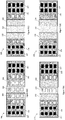
- Figures 2(a)-2(d) illustrate example memory arrays, e.g., a memory array 200, a memory array 210, a memory array 220, and a memory array 230, having a plurality of word lines, in accordance with various embodiments.
- the memory array 200, the memory array 210, the memory array 220, and the memory array 230 may be an example of the memory array 100 as shown in Figure 1(a) .
- the memory array 200 includes a word line plate 208 and a word line plate 209, separated by a slit 205.
- the word line plate 208 intersect with a plurality of pillars 207 in an orthogonal direction
- the word line plate 209 intersect with a plurality of pillars 207 in an orthogonal direction as well.
- the word line plate 208 includes a first material 201 with a first resistivity and a second material 202 with a second resistivity smaller than the first resistivity
- the word line plate 209 includes a first material 203 with a first resistivity and a second material 204 with a second resistivity smaller than the first resistivity.
- the second material 202 is along an edge of the first material 201, and is also disposed at an edge of the slit 205.
- the second material 204 is along an edge of the first material 203, and is also disposed at an edge of the slit 205.
- a plurality of dummy pillars, e.g., dummy pillar 206, are disposed in the first material 201, the second material 202, the first material 203, the second material 204, and the slit 205.
- the memory array 210 includes a word line plate 218 and a word line plate 219, separated by a slit 215.
- the word line plate 218 intersect with a plurality of pillars 217 in an orthogonal direction
- the word line plate 219 intersect with a plurality of pillars 217 in an orthogonal direction as well.
- the word line plate 218 includes a first material 211 with a first resistivity and a second material 212 with a second resistivity smaller than the first resistivity
- the word line plate 219 includes a first material 213 with a first resistivity and a second material 214 with a second resistivity smaller than the first resistivity.
- the second material 212 is along an edge of the first material 211, and is also disposed at an edge of the slit 215.
- the second material 214 is along an edge of the first material 213, and is also disposed at an edge of the slit 215.
- a plurality of dummy pillars, e.g., dummy pillar 216, are disposed in the first material 211, the first material 213, and the slit 215.
- the memory array 220 includes a word line plate 228 and a word line plate 229, separated by a slit 225.
- the word line plate 228 intersect with a plurality of pillars 227 in an orthogonal direction
- the word line plate 229 intersect with a plurality of pillars 227 in an orthogonal direction as well.
- the word line plate 228 includes a first material 221 with a first resistivity and a second material 222 with a second resistivity smaller than the first resistivity
- the word line plate 229 includes a first material 223 with a first resistivity and a second material 224 with a second resistivity smaller than the first resistivity.
- the second material 222 is along an edge of the first material 221, and is also disposed at an edge of the slit 225.
- the second material 224 is along an edge of the first material 223, and is also disposed at an edge of the slit 225.
- a plurality of dummy pillars, e.g., dummy pillar 226, are disposed in the first material 221 and the first material 223.
- the memory array 230 includes a word line plate 238 and a word line plate 239, separated by a slit 235.
- the word line plate 238 intersect with a plurality of pillars 237 in an orthogonal direction
- the word line plate 239 intersect with a plurality of pillars 237 in an orthogonal direction as well.
- the word line plate 238 includes a first material 231 with a first resistivity and a second material 232 with a second resistivity smaller than the first resistivity
- the word line plate 239 includes a first material 233 with a first resistivity and a second material 234 with a second resistivity smaller than the first resistivity.
- the second material 232 is along an edge of the first material 231, and is also disposed at an edge of the slit 235.
- the second material 234 is along an edge of the first material 233, and is also disposed at an edge of the slit 235.
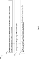
- Figure 3 illustrates an example process 300 for making a memory array having a plurality of word lines, in accordance with various embodiments.
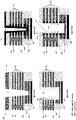
- Figures 4(a)-4(e) illustrate another example process 400 for making a memory array having a plurality of word lines, in accordance with various embodiments.
- the process 300 or the process 400 may be used to form the memory array 100 as shown in Figure 1(a) , the memory array 200, the memory array 210, the memory array 220, and the memory array 230 as shown in Figures 2(a)-2(d) .
- the process 400 may be an example of the process 300 with more details.
- the process 300 may start at a stage 301.
- the process 300 includes forming a plurality of word lines, where a word line includes at least a word line plate comprising a first material with a first resistivity.
- the process 400 includes forming a plurality of word lines, e.g., a word line 401, a word line 403, a word line 405.
- the word line 401, the word line 403, or the word line 405, includes a first material with a first resistivity.
- the word line 401, the word line 403, and the word line 405 are formed above a source line 409 and a SGS transistor 407.
- Insulation layers 402 are formed below, between, and above the word lines.
- the process 400 includes forming a plurality of pillars, e.g., a pillar 404, disposed through the plurality of word lines.
- a pillar includes a number of storage cells formed at an intersection of the pillar and a word line.
- a storage cell includes a channel trapping layer surrounded by the word line, and a cell channel region surrounded by the channel trapping layer.
- the process 400 includes forming a plurality of slits through the plurality of word lines, where a slit separates the plurality of word lines into a first word line region and a second word line region.
- a mask layer 412 is formed above the word lines and the insulation layers.
- An opening 411 is formed as a slit through the word lines, e.g., the word line 401, the word line 403, and the word line 405. In some embodiments, the opening 411 may be further through a part of the layers for the SGS transistor 407.
- the process 300 includes forming a recess along an edge of the word line plate.
- the process 400 includes forming a recess 413 along an edge of the word line plate, e.g., the word line 401, the word line 403, and the word line 404.
- forming the recess along the edge of the word line plate includes forming the recess along the slit, e.g., the opening 411.
- the process 300 includes filling the recess with a second material having a second resistivity that is lower than the first resistivity, to reduce total resistance of the word line.
- the process 400 includes filling the recess 413 with a second material 415 having a second resistivity that is lower than the first resistivity.
- the second material 415 fills a part of the opening 411 as well, and conformally covers a top surface of the insulation layer 402.
- the process 400 may further include removing a part of the second material 415 from the opening 411, and may further removing a part of the second material 415 from the recess 413.
- the process 400 includes filling the opening 411 and a part of the recess 413 by an insulating material 419, which becomes a slit splitting the word lines.
- the second material 415 may fill the entire recess 413, or even extend into a part of the opening 411.
- FIG. 5 illustrates an example computing device suitable for use to practice various aspects of the present disclosure, in accordance with various embodiments.
- the computing device 500 includes system control logic 508 coupled to one or more processor(s) 504, a memory device 512, one or more communications interface(s) 516, and input/output (I/O) devices 520.
- system control logic 508 coupled to one or more processor(s) 504, a memory device 512, one or more communications interface(s) 516, and input/output (I/O) devices 520.
- the memory device 512 may be a non-volatile computer storage chip.
- the memory device 512 comprises a package, driver circuitry (e.g., drivers), input/output connections to electrically couple the memory device 512 with other components of the computing device 500, etc.
- the memory device 512 may be configured to be removably or permanently coupled with the computing device 500.
- the memory device 512 may include a memory device similar to the memory array 100 as shown in Figure 1(a) , the memory array 200, the memory array 210, the memory array 220, and the memory array 230 as shown in Figures 2(a)-2(d) , or a memory array formed according to the process 300 or the process 400.
- Communications interface(s) 516 may provide an interface for computing device 500 to communicate over one or more network(s) and/or with any other suitable device.
- Communications interface(s) 516 may include any suitable hardware and/or firmware.
- Communications interface(s) 516 for one embodiment may include, for example, a network adapter, a wireless network adapter, a telephone modem, and/or a wireless modem.
- communications interface(s) 516 for one embodiment may use one or more antennas to communicatively couple the computing device 500 with a wireless network.
- At least one of the processor(s) 504 may be packaged together with logic for one or more controller(s) of system control logic 508.
- at least one of the processor(s) 504 may be packaged together with logic for one or more controllers of system control logic 508 to form a System in Package (SiP).
- SiP System in Package
- at least one of the processor(s) 504 may be integrated on the same die with logic for one or more controller(s) of system control logic 508.
- at least one of the processor(s) 504 may be integrated on the same die with logic for one or more controller(s) of system control logic 508 to form a System on Chip (SoC).
- SoC System on Chip
- System control logic 508 may include any suitable interface controllers to provide for any suitable interface to at least one of the processor(s) 504 and/or to any suitable device or component in communication with system control logic 508.
- the system control logic 508 may move data into and/or out of the various components of the computing device 500.
- System control logic 508 for one embodiment may include a memory controller 524 configured to provide an interface to the memory device 512, to control various memory access operations.
- the memory controller 524 may include control logic 528 that may be specifically configured to control access of the memory device 512.
- the I/O devices 520 may include user interfaces designed to enable user interaction with the computing device 500, peripheral component interfaces designed to enable peripheral component interaction with the computing device 500, and/or sensors designed to determine environmental conditions and/or location information related to the computing device 500.
- the user interfaces could include, but are not limited to, a display, e.g., a liquid crystal display, a touch screen display, etc., a speaker, a microphone, one or more digital cameras to capture pictures and/or video, a flashlight (e.g., a light emitting diode flash), and a keyboard.
- a display e.g., a liquid crystal display, a touch screen display, etc.
- a speaker e.g., a speaker, a microphone, one or more digital cameras to capture pictures and/or video
- a flashlight e.g., a light emitting diode flash
- a keyboard e.g., a keyboard
- the peripheral component interfaces may include, but are not limited to, a non-volatile memory port, an audio jack, and a power supply interface.
- the sensors may include, but are not limited to, a gyro sensor, an accelerometer, a proximity sensor, an ambient light sensor, and a positioning unit.
- the positioning unit may additionally/alternatively be part of, or interact with, the communication interface(s) 516 to communicate with components of a positioning network, e.g., a global positioning system (GPS) satellite.
- GPS global positioning system
- the computing device 500 may be a server; a laptop computing device, a tablet computing device, a netbook, a smartphone, etc.; a desktop computing device; a workstation; etc.
- the computing device 500 may have more or fewer components, and/or different architectures.
- the computing device 500 may be any other electronic device that processes data.
- Figure 6 illustrates a storage medium having instructions for practicing methods described with references to Figures 1-5 , in accordance with various embodiments.
- the instructions stored on the computing device-readable medium 602 may be executed, for example, on the processor(s) 504 of the computing device 500 of Figure 5 .
- the computing device-readable storage medium 802 may be implemented in, or be accessible by, the control logic 528 of Figure 5 .
- computing device-readable storage medium 602 may include the executable code of a number of programming instructions or bit streams 604.
- Executable code of programming instructions (or bit streams) 604 may be configured to enable a device, e.g., computing device 600, in response to execution of the executable code/programming instructions to perform (aspects of) processes the process 300 or the process 400.
- executable code/programming instructions/bit streams 604 may be disposed on multiple non-transitory computing device-readable storage media 602 instead.
- computing device-readable storage medium 602 may be non-transitory.
- executable code/programming instructions 604 may be encoded in a transitory computer readable medium, such as signals.
Landscapes
- Engineering & Computer Science (AREA)
- Microelectronics & Electronic Packaging (AREA)
- Semiconductor Memories (AREA)
- Non-Volatile Memory (AREA)
- Physics & Mathematics (AREA)
- Geometry (AREA)
Abstract
Description
- Embodiments of the present disclosure relate generally to the technical fields of computing devices, and more particularly to the memory devices.
- The background description provided herein is for the purpose of generally presenting the context of the disclosure. Unless otherwise indicated herein, the materials described in this section are not prior art to the claims in this application and are not admitted to be prior art by inclusion in this section.
- Memory devices are important parts of integrated circuits (IC) and modern electronic devices. A typical memory device, e.g., a flash memory device or a dynamic random access memory (DRAM), comprise a memory array that includes a large number of memory cells arranged in row and column fashion controlled by word lines and bit lines, where data may be stored in the memory cells. However, current memory array architecture may have high word line (WL) resistance, which may result in technological restrictions on the memory structures occupying a particular die area.
- Embodiments will be readily understood by the following detailed description in conjunction with the accompanying drawings. To facilitate this description, like reference numerals designate like structural elements. Embodiments are illustrated by way of example and not by way of limitation in the figures of the accompanying drawings.
-
Figures 1(a)-1(d) illustrate an example apparatus including a memory array having a plurality of word lines, in accordance with various embodiments. -
Figures 2(a)-2(d) illustrate example memory arrays having a plurality of word lines, in accordance with various embodiments. -
Figure 3 illustrates an example process for making a memory array having a plurality of word lines, in accordance with various embodiments. -
Figures 4(a)-4(e) illustrate another example process making a memory array having a plurality of word lines, in accordance with various embodiments. -
Figure 5 illustrates an example computing device suitable for use to practice various aspects of the present disclosure, in accordance with various embodiments. -
Figure 6 illustrates a storage medium having instructions for practicing methods described with references toFigures 1-5 , in accordance with various embodiments. - Embodiments herein include a memory array having a plurality of word lines. A word line includes at least one word line plate, and the word line plate comprises a first material with a first resistivity. An edge of the word line plate is recessed and filled with a second material having a second resistivity that is lower than the first resistivity. As a result, the total resistance of the word line may be reduced compared to a word line using only the first material with the first resistivity.
- Embodiments herein include a method for forming a memory array. The method includes forming a plurality of word lines. A word line includes at least a word line plate comprising a first material with a first resistivity. The method further includes forming a recess along an edge of the word line plate; and filling the recess with a second material having a second resistivity that is lower than the first resistivity. As a result, the total resistance of the word line may be reduced compared to a word line using only the first material with the first resistivity.
- Embodiments herein include a computing device. The computing device includes one or more processors, and a memory array attached to the one or more processors. The memory array includes a plurality of word lines. A word line includes at least one word line plate, and the word line plate comprises a first material with a first resistivity. An edge of the word line plate is recessed and filled with a second material having a second resistivity that is lower than the first resistivity. As a result, the total resistance of the word line may be reduced compared to a word line using only the first material with the first resistivity.
- Memory devices are important parts of integrated circuits (IC), computing devices, or modern electronic devices. Nonvolatile memory, such as NAND based flash memory, has become a widely used storage memory for various devices and systems. A memory device comprise a memory array that includes a large number of memory cells arranged in row and column fashion controlled by word lines (WL) and bit lines, where data may be stored in the memory cells. However, in current technology, word lines may have high resistances, which may restrict the length of WL, resulting in die area penalty, frequent WL chopping, more staircases and block separations. When a word line includes polysilicon, in order to reduce the resistance of the polysilicon, increasing polysilicon dopants or silicidation of polysilicon may be used. However, increasing dopants in polysilicon for a word line may not be enough to lower its resistance to impact die area to a desired size. In addition, increasing dopants in polysilicon may make it difficult to control uniform dielectric growth for the memory cells. Silicidation of polysilicon is also self-limited, resulting in more word line plate separation and larger die size to expose the polysilicon to be silicided.
- Embodiments described herein use a word line plate including two different materials with two different resistivity. For example, the word line plate comprises a first material with a first resistivity, and a second material having a second resistivity that is lower than the first resistivity, to reduce total resistance of the word line. The second material may be placed along an edge of the first material. The first material may include polysilicon, and the second material may include a metal, e.g., W, Mo, Ti, TiN, or other metals. Such word lines may be applied to many different kinds of memory array architecture, e.g., a 2 dimensional NAND memory array, a 3 dimensional NAND memory array, some other flash memory device, or other memory devices. Embodiments herein also include processes for making such a memory array with word lines. The process includes shunting low resistive material to an edge of a polysilicon word line plate. At the edge of a word line plate, metallic material can be detected, while the polysilicon part of the word line may be inside the memory array block. By using metallic material along an edge of a word line plate, the word line may have reduced RC delays. Accordingly, the reduced RC delay allows extended word line length and reduced die size scaling by eliminating staircase, or memory block to block separation area. As a further result, the number of drain-side select gate (SGD) or source-side select gate (SSG) may be reduced as well.
- In the description to follow, reference is made to the accompanying drawings that form a part hereof wherein like numerals designate like parts throughout, and in which is shown by way of illustration embodiments that may be practiced. It is to be understood that other embodiments may be utilized and structural or logical changes may be made without departing from the scope of the present disclosure. Therefore, the following detailed description is not to be taken in a limiting sense, and the scope of embodiments is defined by the appended claims and their equivalents.
- Operations of various methods may be described as multiple discrete actions or operations in turn, in a manner that is most helpful in understanding the claimed subject matter. However, the order of description should not be construed as to imply that these operations are necessarily order dependent. In particular, these operations may not be performed in the order of presentation. Operations described may be performed in a different order than the described embodiments. Various additional operations may be performed and/or described operations may be omitted, split or combined in additional embodiments.
- For the purposes of the present disclosure, the phrase "A or B" and "A and/or B" means (A), (B), or (A and B). For the purposes of the present disclosure, the phrase "A, B, and/or C" means (A), (B), (C), (A and B), (A and C), (B and C), or (A, B and C).
- The description may use the phrases "in an embodiment," or "in embodiments," which may each refer to one or more of the same or different embodiments. Furthermore, the terms "comprising," "including," "having," and the like, as used with respect to embodiments of the present disclosure, are synonymous.
- Where the disclosure recites "a" or "a first" element or the equivalent thereof, such disclosure includes one or more such elements, neither requiring nor excluding two or more such elements. Further, ordinal indicators (e.g., first, second or third) for identified elements are used to distinguish between the elements, and do not indicate or imply a required or limited number of such elements, nor do they indicate a particular position or order of such elements unless otherwise specifically stated.
- As used herein, the term "circuitry" may refer to, is part of, or includes hardware components such as an electronic circuit, a logic circuit, a processor (shared, dedicated, or group) and/or memory (shared, dedicated, or group), an Application Specific Integrated Circuit (ASIC), a field-programmable device (FPD), (for example, a field-programmable gate array (FPGA), a programmable logic device (PLD), a complex PLD (CPLD), a high-capacity PLD (HCPLD), a structured ASIC, or a programmable System on Chip (SoC)), digital signal processors (DSPs), etc., that are configured to provide the described functionality. In some embodiments, the circuitry may execute one or more software or firmware programs to provide at least some of the described functionality.
- As used herein, the term "processor circuitry" may refer to, is part of, or includes circuitry capable of sequentially and automatically carrying out a sequence of arithmetic or logical operations; recording, storing, and/or transferring digital data. The term "processor circuitry" may refer to one or more application processors, one or more baseband processors, a physical central processing unit (CPU), a single-core processor, a dual-core processor, a triple-core processor, a quad-core processor, and/or any other device capable of executing or otherwise operating computer-executable instructions, such as program code, software modules, and/or functional processes.
- As used herein, the term "computer device" or "computing device" may describe any physical hardware device capable of sequentially and automatically carrying out a sequence of arithmetic or logical operations, equipped to record/store data on a machine readable medium, and transmit and receive data from one or more other devices in a communications network. A computer device may be considered synonymous to, and may hereafter be occasionally referred to, as a computer, computing platform, computing device, etc. The term "computer system" may include any type interconnected electronic devices, computer devices, or components thereof. Additionally, the term "computer system" and/or "system" may refer to various components of a computer that are communicatively coupled with one another. Furthermore, the term "computer system" and/or "system" may refer to multiple computer devices and/or multiple computing systems that are communicatively coupled with one another and configured to share computing and/or networking resources. Examples of "computer devices", "computer systems", etc. may include cellular phones or smart phones, feature phones, tablet personal computers, wearable computing devices, an autonomous sensors, laptop computers, desktop personal computers, video game consoles, digital media players, handheld messaging devices, personal data assistants, an electronic book readers, augmented reality devices, server computer devices (e.g., stand-alone, rack-mounted, blade, etc.), cloud computing services/systems, network elements, in-vehicle infotainment (IVI), in-car entertainment (ICE) devices, an Instrument Cluster (IC), head-up display (HUD) devices, onboard diagnostic (OBD) devices, dashtop mobile equipment (DME), mobile data terminals (MDTs), Electronic Engine Management Systems (EEMSs), electronic/engine control units (ECUs), vehicle-embedded computer devices (VECDs), autonomous or semi-autonomous driving vehicle (hereinafter, simply ADV) systems, in-vehicle navigation systems, electronic/engine control modules (ECMs), embedded systems, microcontrollers, control modules, engine management systems (EMS), networked or "smart" appliances, machine-type communications (MTC) devices, machine-to-machine (M2M), Internet of Things (IoT) devices, and/or any other like electronic devices. Moreover, the term "vehicle-embedded computer device" may refer to any computer device and/or computer system physically mounted on, built in, or otherwise embedded in a vehicle.
-
Figures 1(a)-1(d) illustrate an example apparatus including amemory array 100 having a plurality of word lines, in accordance with various embodiments. Thememory array 100 may be a part of a 3D NAND flash memory, a three dimensional double density flash memory, a vertical flash memory, or a horizontal flash memory. Thememory array 100 is only for illustration, and is not limiting. For example, there may be another memory array that is a two dimensional NAND flash memory array having a plurality of word lines. - In embodiments, as shown in
Figure 1(a) , thememory array 100 includes multiple conductive layers to function as word lines, e.g., aword line 101, aword line 103. Insulation layers, e.g., aninsulation layer 102, such as an oxide, are positioned between the word lines. There may be more than two word lines in a memory array. The word lines and the insulation layers may be placed in a first direction, e.g., the Y direction. In embodiments, aslit 107 splits each word line, e.g., theword line 101, theword line 103, into two word line regions. For example, theword line 101 is split by theslit 107 into aregion 111 and aregion 113. There is alayer 105 below theword line 103 and separated from theword line 103 by aninsulation layer 104. Thelayer 105 may include a source side select (SGS) transistor, which may be referred to as a source select gate (SSG), coupled to a source line. There may be a drain side select (SGD) transistor, which may be referred to as a drain select gate, not shown, above theword line 101. Theslit 107 may be filled with an insulating material, not shown. In some embodiments, there may not be any slit. - In embodiments, the
word line 101 includes multiple word line plates, e.g., a word line plate for theregion 111, and a word line plate for theregion 113. As shown inFigure 1(b) , the word line plate for theregion 111 may include afirst material 119 with a first resistivity, and asecond material 115 having a second resistivity that is lower than the first resistivity. Thesecond material 115 may be formed along an edge of thefirst material 119. In addition, thesecond material 115 is also disposed at an edge of theslit 107. For example, an edge of the word line plate for theregion 111 is recessed and filled with thesecond material 115. In some embodiments, there may be anothermaterial 117 along another side of thefirst material 119. Since the resistivity of the material 117 or thesecond material 115 is smaller than the resistivity of thefirst material 119, the total resistance of theword line region 111 may be reduced, compared to a word line region using only the first material. As shown inFigure 1(b) , the total resistance of theword line region 111 is a result of three parallel resistances for thefirst material 119, the resistance for thesecond material 115, and a resistance of thematerial 117. Thematerial 117 may be a same material as thesecond material 115, or a different material. In some embodiments, the first material includes polysilicon, and the second material includes a metal material, e.g., W, Ti, TiN, Mo, or other metals. In some embodiments, there may only two different materials, thefirst material 119 and thesecond material 115, without thematerial 117. - For the example shown in
Figure 1(b) , the total resistance of the word line plate having thesecond material 115 and thematerial 117 on two sides of thefirst material 119 can be about 4 times lower than a word line plate including only polysilicon. Accordingly, with a same RC, a word line plate as shown inFigure 1(b) can have about twice length of a word line plate with only polysilicon. - One or more pillars, e.g., a
pillar 122, apillar 124, apillar 126, and apillar 128, may be disposed through the plurality of word lines along a second direction orthogonal to the first direction, e.g., the Z direction. In some embodiments, a pillar may be referred to as a string. Thememory array 100 further includes a plurality of bit lines, e.g., abit line 121, abit line 123, coupled to the plurality of pillars in a direction, e.g., the X direction, orthogonal to the plurality of word lines and the plurality of pillars. A pillar may be an active pillar including a number of storage cells, or a dummy pillar that does not include a storage cell. The storage cells of the pillars, e.g., thepillar 122, are selected by drain select gates to connect to the bit lines for read and write operations. - For example, as shown in
Figure 1(c) , thepillar 122 may include astorage cell 132 at the intersection of theword line 101 and thepillar 122, and astorage cell 134 at the intersection of theword line 103 and thepillar 122. Thepillar 122 is coupled to thebit line 121 through a drainselect gate 141, and coupled to the sourceselect gate 143 and further coupled to thesource line 105. - Each storage cell is formed at the intersection of a WL and an active pillar. For example, as shown in
Figure 1(d) , thestorage cell 132 is formed at the intersection of theword line 101 and thepillar 122. Thestorage cell 132 may include a floating gate transistor. Thestorage cell 132 includes achannel trapping layer 112 surrounded by theword line 101, and acell channel region 114 surrounded by thechannel trapping layer 112. Thechannel trapping layer 112 may include an oxide-nitride-oxide (ONO) material. In some embodiments, there may be anoxide material 116 surrounded by thecell channel region 114. Some of the pillars, e.g., thepillar 128, may be a dummy pillar disposed through the plurality of word lines, where thedummy pillar 128 does not include a storage cell. - In some embodiments, the
storage cell 132 may represent one-bit data 118 for a single-level-cell (SLC) structure. In some other embodiments, thestorage cell 132 may also have multiple-level-cell (MLC) structures or triple-level-cell (TLC) structures that store 2 or 3 bits, respectively, at each cell. As shown inFigure 1(a) , theslit 107 splits each word line into two regions coupled to the same bit line. This allows for each cell to store double the data. In general, a slit separates the plurality of word lines into a first word line region and a second word line region, and storage cells within the first word line region forms a first memory block, and storage cells within the second word line region forms a second memory block. -
Figures 2(a)-2(d) illustrate example memory arrays, e.g., amemory array 200, amemory array 210, amemory array 220, and amemory array 230, having a plurality of word lines, in accordance with various embodiments. Thememory array 200, thememory array 210, thememory array 220, and thememory array 230 may be an example of thememory array 100 as shown inFigure 1(a) . - In embodiments, as shown in
Figure 2(a) , thememory array 200 includes aword line plate 208 and aword line plate 209, separated by aslit 205. Theword line plate 208 intersect with a plurality ofpillars 207 in an orthogonal direction, and theword line plate 209 intersect with a plurality ofpillars 207 in an orthogonal direction as well. Theword line plate 208 includes afirst material 201 with a first resistivity and asecond material 202 with a second resistivity smaller than the first resistivity, and theword line plate 209 includes afirst material 203 with a first resistivity and asecond material 204 with a second resistivity smaller than the first resistivity. Thesecond material 202 is along an edge of thefirst material 201, and is also disposed at an edge of theslit 205. Thesecond material 204 is along an edge of thefirst material 203, and is also disposed at an edge of theslit 205. A plurality of dummy pillars, e.g.,dummy pillar 206, are disposed in thefirst material 201, thesecond material 202, thefirst material 203, thesecond material 204, and theslit 205. - In embodiments, as shown in
Figure 2(b) , thememory array 210 includes aword line plate 218 and aword line plate 219, separated by aslit 215. Theword line plate 218 intersect with a plurality ofpillars 217 in an orthogonal direction, and theword line plate 219 intersect with a plurality ofpillars 217 in an orthogonal direction as well. Theword line plate 218 includes afirst material 211 with a first resistivity and asecond material 212 with a second resistivity smaller than the first resistivity, and theword line plate 219 includes afirst material 213 with a first resistivity and asecond material 214 with a second resistivity smaller than the first resistivity. Thesecond material 212 is along an edge of thefirst material 211, and is also disposed at an edge of theslit 215. Thesecond material 214 is along an edge of thefirst material 213, and is also disposed at an edge of theslit 215. A plurality of dummy pillars, e.g.,dummy pillar 216, are disposed in thefirst material 211, thefirst material 213, and theslit 215. - In embodiments, as shown in
Figure 2(c) , thememory array 220 includes aword line plate 228 and aword line plate 229, separated by aslit 225. Theword line plate 228 intersect with a plurality ofpillars 227 in an orthogonal direction, and theword line plate 229 intersect with a plurality ofpillars 227 in an orthogonal direction as well. Theword line plate 228 includes afirst material 221 with a first resistivity and asecond material 222 with a second resistivity smaller than the first resistivity, and theword line plate 229 includes afirst material 223 with a first resistivity and asecond material 224 with a second resistivity smaller than the first resistivity. Thesecond material 222 is along an edge of thefirst material 221, and is also disposed at an edge of theslit 225. Thesecond material 224 is along an edge of thefirst material 223, and is also disposed at an edge of theslit 225. A plurality of dummy pillars, e.g.,dummy pillar 226, are disposed in thefirst material 221 and thefirst material 223. - In embodiments, as shown in
Figure 2(d) , thememory array 230 includes aword line plate 238 and aword line plate 239, separated by aslit 235. Theword line plate 238 intersect with a plurality ofpillars 237 in an orthogonal direction, and theword line plate 239 intersect with a plurality ofpillars 237 in an orthogonal direction as well. Theword line plate 238 includes afirst material 231 with a first resistivity and asecond material 232 with a second resistivity smaller than the first resistivity, and theword line plate 239 includes afirst material 233 with a first resistivity and asecond material 234 with a second resistivity smaller than the first resistivity. Thesecond material 232 is along an edge of thefirst material 231, and is also disposed at an edge of theslit 235. Thesecond material 234 is along an edge of thefirst material 233, and is also disposed at an edge of theslit 235. -
Figure 3 illustrates anexample process 300 for making a memory array having a plurality of word lines, in accordance with various embodiments.Figures 4(a)-4(e) illustrate anotherexample process 400 for making a memory array having a plurality of word lines, in accordance with various embodiments. Theprocess 300 or theprocess 400 may be used to form thememory array 100 as shown inFigure 1(a) , thememory array 200, thememory array 210, thememory array 220, and thememory array 230 as shown inFigures 2(a)-2(d) . Theprocess 400 may be an example of theprocess 300 with more details. - The
process 300 may start at astage 301. During thestage 301, theprocess 300 includes forming a plurality of word lines, where a word line includes at least a word line plate comprising a first material with a first resistivity. For example, as shown inFigure 4(a) , theprocess 400 includes forming a plurality of word lines, e.g., aword line 401, aword line 403, aword line 405. Theword line 401, theword line 403, or theword line 405, includes a first material with a first resistivity. In addition, theword line 401, theword line 403, and theword line 405 are formed above asource line 409 and aSGS transistor 407. Insulation layers 402 are formed below, between, and above the word lines. In addition, theprocess 400 includes forming a plurality of pillars, e.g., apillar 404, disposed through the plurality of word lines. A pillar includes a number of storage cells formed at an intersection of the pillar and a word line. A storage cell includes a channel trapping layer surrounded by the word line, and a cell channel region surrounded by the channel trapping layer. Moreover, theprocess 400 includes forming a plurality of slits through the plurality of word lines, where a slit separates the plurality of word lines into a first word line region and a second word line region. In detail, amask layer 412 is formed above the word lines and the insulation layers. Anopening 411 is formed as a slit through the word lines, e.g., theword line 401, theword line 403, and theword line 405. In some embodiments, theopening 411 may be further through a part of the layers for theSGS transistor 407. - During a
stage 303, theprocess 300 includes forming a recess along an edge of the word line plate. For example, as shown inFigure 4(b) , theprocess 400 includes forming arecess 413 along an edge of the word line plate, e.g., theword line 401, theword line 403, and theword line 404. In embodiments, forming the recess along the edge of the word line plate includes forming the recess along the slit, e.g., theopening 411. - During a
stage 305, theprocess 300 includes filling the recess with a second material having a second resistivity that is lower than the first resistivity, to reduce total resistance of the word line. For example, as shown inFigure 4(c) , theprocess 400 includes filling therecess 413 with asecond material 415 having a second resistivity that is lower than the first resistivity. Thesecond material 415 fills a part of theopening 411 as well, and conformally covers a top surface of theinsulation layer 402. - In addition, as shown in
Figure 4(d) , theprocess 400 may further include removing a part of thesecond material 415 from theopening 411, and may further removing a part of thesecond material 415 from therecess 413. Moreover, as shown inFigure 4(e) , theprocess 400 includes filling theopening 411 and a part of therecess 413 by an insulatingmaterial 419, which becomes a slit splitting the word lines. In some other embodiments, thesecond material 415 may fill theentire recess 413, or even extend into a part of theopening 411. -
Figure 5 illustrates an example computing device suitable for use to practice various aspects of the present disclosure, in accordance with various embodiments. Thecomputing device 500 includessystem control logic 508 coupled to one or more processor(s) 504, amemory device 512, one or more communications interface(s) 516, and input/output (I/O)devices 520. - The
memory device 512 may be a non-volatile computer storage chip. In embodiments, thememory device 512 comprises a package, driver circuitry (e.g., drivers), input/output connections to electrically couple thememory device 512 with other components of thecomputing device 500, etc. Thememory device 512 may be configured to be removably or permanently coupled with thecomputing device 500. In some embodiments, thememory device 512 may include a memory device similar to thememory array 100 as shown inFigure 1(a) , thememory array 200, thememory array 210, thememory array 220, and thememory array 230 as shown inFigures 2(a)-2(d) , or a memory array formed according to theprocess 300 or theprocess 400. - Communications interface(s) 516 may provide an interface for
computing device 500 to communicate over one or more network(s) and/or with any other suitable device. Communications interface(s) 516 may include any suitable hardware and/or firmware. Communications interface(s) 516 for one embodiment may include, for example, a network adapter, a wireless network adapter, a telephone modem, and/or a wireless modem. For wireless communications, communications interface(s) 516 for one embodiment may use one or more antennas to communicatively couple thecomputing device 500 with a wireless network. - For one embodiment, at least one of the processor(s) 504 may be packaged together with logic for one or more controller(s) of
system control logic 508. For one embodiment, at least one of the processor(s) 504 may be packaged together with logic for one or more controllers ofsystem control logic 508 to form a System in Package (SiP). For one embodiment, at least one of the processor(s) 504 may be integrated on the same die with logic for one or more controller(s) ofsystem control logic 508. For one embodiment, at least one of the processor(s) 504 may be integrated on the same die with logic for one or more controller(s) ofsystem control logic 508 to form a System on Chip (SoC). -
System control logic 508 for one embodiment may include any suitable interface controllers to provide for any suitable interface to at least one of the processor(s) 504 and/or to any suitable device or component in communication withsystem control logic 508. Thesystem control logic 508 may move data into and/or out of the various components of thecomputing device 500. -
System control logic 508 for one embodiment may include amemory controller 524 configured to provide an interface to thememory device 512, to control various memory access operations. Thememory controller 524 may includecontrol logic 528 that may be specifically configured to control access of thememory device 512. - In various embodiments, the I/
O devices 520 may include user interfaces designed to enable user interaction with thecomputing device 500, peripheral component interfaces designed to enable peripheral component interaction with thecomputing device 500, and/or sensors designed to determine environmental conditions and/or location information related to thecomputing device 500. - In various embodiments, the user interfaces could include, but are not limited to, a display, e.g., a liquid crystal display, a touch screen display, etc., a speaker, a microphone, one or more digital cameras to capture pictures and/or video, a flashlight (e.g., a light emitting diode flash), and a keyboard.
- In various embodiments, the peripheral component interfaces may include, but are not limited to, a non-volatile memory port, an audio jack, and a power supply interface. In various embodiments, the sensors may include, but are not limited to, a gyro sensor, an accelerometer, a proximity sensor, an ambient light sensor, and a positioning unit. The positioning unit may additionally/alternatively be part of, or interact with, the communication interface(s) 516 to communicate with components of a positioning network, e.g., a global positioning system (GPS) satellite.
- In various embodiments, the
computing device 500 may be a server; a laptop computing device, a tablet computing device, a netbook, a smartphone, etc.; a desktop computing device; a workstation; etc. Thecomputing device 500 may have more or fewer components, and/or different architectures. In further implementations, thecomputing device 500 may be any other electronic device that processes data. -
Figure 6 illustrates a storage medium having instructions for practicing methods described with references toFigures 1-5 , in accordance with various embodiments. Theinstructions 604 stored on the computing device-readable medium 602. More specifically, the computing device-readable medium 602 may include a memory device similar to thememory array 100 as shown inFigure 1(a) , thememory array 200, thememory array 210, thememory array 220, and thememory array 230 as shown inFigures 2(a)-2(d) , or a memory array formed according to theprocess 300 or theprocess 400. The instructions stored on the computing device-readable medium 602 may be executed, for example, on the processor(s) 504 of thecomputing device 500 ofFigure 5 . The computing device-readable storage medium 802 may be implemented in, or be accessible by, thecontrol logic 528 ofFigure 5 . - As illustrated, computing device-
readable storage medium 602 may include the executable code of a number of programming instructions or bit streams 604. Executable code of programming instructions (or bit streams) 604 may be configured to enable a device, e.g.,computing device 600, in response to execution of the executable code/programming instructions to perform (aspects of) processes theprocess 300 or theprocess 400. In alternate embodiments, executable code/programming instructions/bit streams 604 may be disposed on multiple non-transitory computing device-readable storage media 602 instead. In embodiments, computing device-readable storage medium 602 may be non-transitory. In still other embodiments, executable code/programming instructions 604 may be encoded in a transitory computer readable medium, such as signals. - Thus various example embodiments of the present disclosure have been described including, but are not limited to:
- Example 1 may include an apparatus comprising: a memory array including a plurality of word lines, wherein a word line includes at least one word line plate, wherein the word line plate comprises a first material with a first resistivity, wherein an edge of the word line plate is recessed and filled with a second material having a second resistivity that is lower than the first resistivity, to reduce total resistance of the word line.
- Example 2 may include the apparatus of example 1 and/or some other examples herein, wherein the first material includes polysilicon, and the second material includes a metal.
- Example 3 may include the apparatus of example 1 and/or some other examples herein, wherein memory array further includes a plurality of pillars disposed through the plurality of word lines, wherein a pillar includes a number of storage cells, a storage cell includes a channel trapping layer surrounded by the word line, and a cell channel region surrounded by the channel trapping layer.
- Example 4 may include the apparatus of example 3 and/or some other examples herein, wherein the storage cell includes a floating gate transistor.
- Example 5 may include the apparatus of example 3 and/or some other examples herein, wherein the channel trapping layer includes an Oxide-Nitride-Oxide (ONO) material.
- Example 6 may include the apparatus of example 3 and/or some other examples herein, wherein the storage cell further includes an oxide material surrounded by the cell channel region.
- Example 7 may include the apparatus of example 3 and/or some other examples herein, wherein the memory array further includes a plurality of slits through the plurality of word lines, and wherein a slit separates the plurality of word lines into a first word line region and a second word line region, and storage cells within the first word line region forms a first memory block, and storage cells within the second word line region forms a second memory block.
- Example 8 may include the apparatus of example 7 and/or some other examples herein, wherein the slit is filled with an insulating material.
- Example 9 may include the apparatus of example 3 and/or some other examples herein, wherein the memory array further includes a source side select (SGS) transistor or a drain side select (SGD) transistor above or below the plurality of the word lines.
- Example 10 may include the apparatus of example 3 and/or some other examples herein, wherein the memory array further includes a plurality of bit lines coupled to the plurality of pillars in a direction orthogonal to the plurality of word lines and the plurality of pillars.
- Example 11 may include a method for forming a memory array, the method comprising: forming a plurality of word lines, wherein a word line includes at least a word line plate comprising a first material with a first resistivity; forming a recess along an edge of the word line plate; and filling the recess with a second material having a second resistivity that is lower than the first resistivity, to reduce total resistance of the word line.
- Example 12 may include the method of example 11 and/or some other examples herein, wherein the first material includes polysilicon, and the second material includes a metal.
- Example 13 may include the method of example 11 and/or some other examples herein, further comprises: forming a plurality of pillars disposed through the plurality of word lines, wherein a pillar includes a number of storage cells, a storage cell includes a channel trapping layer surrounded by the word line, and a cell channel region surrounded by the channel trapping layer.
- Example 14 may include the method of example 11 and/or some other examples herein, further comprises: forming one or more dummy pillars disposed through the plurality of word lines, wherein a dummy pillar does not include a storage cell.
- Example 15 may include the method of example 11 and/or some other examples herein, further comprising: forming a plurality of slits through the plurality of word lines, wherein a slit separates the plurality of word lines into a first word line region and a second word line region, and wherein the forming the recess along the edge of the word line plate includes forming the recess along the slit.
- Example 16 may include the method of example 15 and/or some other examples herein, wherein the second material filling the recess along the edge of the word line plate is also disposed along an edge of the slit.
- Example 17 may include a computing device, comprising: one or more processors; and a memory array coupled to the one or more processors, wherein the memory array includes a plurality of word lines, wherein a word line includes at least one word line plate, wherein the word line plate comprises a first material with a first resistivity, wherein an edge of the word line plate is recessed and filled with a second material having a second resistivity that is lower than the first resistivity, to reduce total resistance of the word line.
- Example 18 may include the computing device of example 17 and/or some other examples herein, wherein the memory array is a three dimensional double density flash memory.
- Example 19 may include the computing device of example 17 and/or some other examples herein, wherein the first material includes polysilicon, and the second material includes a metal; and wherein the memory array further includes a plurality of pillars disposed through the plurality of word lines, wherein a pillar includes a number of storage cells, a storage cell includes a channel trapping layer surrounded by the word line, and a cell channel region surrounded by the channel trapping layer.
- Example 20 may include the computing device of example 19 and/or some other examples herein, wherein the memory array further includes a plurality of slits through the plurality of word lines, and wherein a slit separates the plurality of word lines into a first word line region and a second word line region, and storage cells within the first word line region forms a first memory block, and storage cells within the second word line region forms a second memory block.
- Although certain embodiments have been illustrated and described herein for purposes of description this application is intended to cover any adaptations or variations of the embodiments discussed herein. Therefore, it is manifestly intended that embodiments described herein be limited only by the claims.
Claims (15)
- An apparatus comprising:
a memory array including a plurality of word lines, wherein a word line includes at least one word line plate, wherein the word line plate comprises a first material with a first resistivity, wherein an edge of the word line plate is recessed and filled with a second material having a second resistivity that is lower than the first resistivity, to reduce total resistance of the word line. - The apparatus of claim 1, wherein the first material includes polysilicon, and the second material includes a metal.
- The apparatus of claim 1, wherein memory array further includes a plurality of pillars disposed through the plurality of word lines, wherein a pillar includes a number of storage cells, a storage cell includes a channel trapping layer surrounded by the word line, and a cell channel region surrounded by the channel trapping layer.
- The apparatus of claim 3, wherein the channel trapping layer includes an Oxide-Nitride-Oxide (ONO) material.
- The apparatus of claim 3, wherein the storage cell further includes an oxide material surrounded by the cell channel region.
- The apparatus of claim 3, wherein the memory array further includes a plurality of slits through the plurality of word lines, and wherein a slit separates the plurality of word lines into a first word line region and a second word line region, and storage cells within the first word line region forms a first memory block, and storage cells within the second word line region forms a second memory block, wherein the slit is filled with an insulating material.
- The apparatus of claim 3, wherein the memory array further includes a source side select (SGS) transistor or a drain side select (SGD) transistor above or below the plurality of the word lines.
- The apparatus of claim 3, wherein the memory array further includes a plurality of bit lines coupled to the plurality of pillars in a direction orthogonal to the plurality of word lines and the plurality of pillars.
- A method for forming a memory array, the method comprising:forming a plurality of word lines, wherein a word line includes at least a word line plate comprising a first material with a first resistivity;forming a recess along an edge of the word line plate; andfilling the recess with a second material having a second resistivity that is lower than the first resistivity, to reduce total resistance of the word line.
- The method of claim 9, further comprising:
forming a plurality of pillars disposed through the plurality of word lines, wherein a pillar includes a number of storage cells, a storage cell includes a channel trapping layer surrounded by the word line, and a cell channel region surrounded by the channel trapping layer. - The method of claim 9, further comprising:
forming one or more dummy pillars disposed through the plurality of word lines, wherein a dummy pillar does not include a storage cell. - The method of claim 9, further comprising:
forming a plurality of slits through the plurality of word lines, wherein a slit separates the plurality of word lines into a first word line region and a second word line region, and wherein the forming the recess along the edge of the word line plate includes forming the recess along the slit. - A computing device, comprising:one or more processors; anda memory array coupled to the one or more processors, wherein the memory array includes a plurality of word lines, wherein a word line includes at least one word line plate, wherein the word line plate comprises a first material with a first resistivity, wherein an edge of the word line plate is recessed and filled with a second material having a second resistivity that is lower than the first resistivity, to reduce total resistance of the word line.
- The computing device of claim 13, wherein the first material includes polysilicon, and the second material includes a metal; and wherein the memory array further includes a plurality of pillars disposed through the plurality of word lines, wherein a pillar includes a number of storage cells, a storage cell includes a channel trapping layer surrounded by the word line, and a cell channel region surrounded by the channel trapping layer.
- The computing device of claim 14, wherein the memory array further includes a plurality of slits through the plurality of word lines, and wherein a slit separates the plurality of word lines into a first word line region and a second word line region, and storage cells within the first word line region forms a first memory block, and storage cells within the second word line region forms a second memory block.
Applications Claiming Priority (1)
| Application Number | Priority Date | Filing Date | Title |
|---|---|---|---|
| US16/799,448 US11587874B2 (en) | 2020-02-24 | 2020-02-24 | Resistance reduction for word lines in memory arrays |
Publications (2)
| Publication Number | Publication Date |
|---|---|
| EP3869510A1 true EP3869510A1 (en) | 2021-08-25 |
| EP3869510B1 EP3869510B1 (en) | 2023-12-20 |
Family
ID=73497509
Family Applications (1)
| Application Number | Title | Priority Date | Filing Date |
|---|---|---|---|
| EP20208294.7A Active EP3869510B1 (en) | 2020-02-24 | 2020-11-18 | Resistance reduction for word lines in memory arrays |
Country Status (3)
| Country | Link |
|---|---|
| US (1) | US11587874B2 (en) |
| EP (1) | EP3869510B1 (en) |
| KR (1) | KR20210107524A (en) |
Families Citing this family (2)
| Publication number | Priority date | Publication date | Assignee | Title |
|---|---|---|---|---|
| KR20230011748A (en) * | 2021-07-14 | 2023-01-25 | 삼성전자주식회사 | Semiconductor device and Memory system comprising the same |
| WO2023018190A1 (en) | 2021-08-13 | 2023-02-16 | Lg Energy Solution, Ltd. | Negative electrode active material, and negative electrode and secondary battery including same |
Citations (3)
| Publication number | Priority date | Publication date | Assignee | Title |
|---|---|---|---|---|
| US20120146122A1 (en) * | 2010-12-14 | 2012-06-14 | Sung Jin Whang | 3-d non-volatile memory device and method of manufacturing the same |
| US20130043509A1 (en) * | 2011-08-16 | 2013-02-21 | Sung Yoon Cho | 3-d structured non-volatile memory device and method of manufacturing the same |
| US9735202B1 (en) * | 2016-02-16 | 2017-08-15 | Sandisk Technologies Llc | Implementation of VMCO area switching cell to VBL architecture |
Family Cites Families (4)
| Publication number | Priority date | Publication date | Assignee | Title |
|---|---|---|---|---|
| KR102002802B1 (en) * | 2012-09-05 | 2019-07-23 | 삼성전자주식회사 | Semiconductor device |
| KR102031622B1 (en) * | 2013-01-18 | 2019-10-14 | 삼성전자주식회사 | Vertical type semiconductor device |
| TWI669806B (en) * | 2017-02-07 | 2019-08-21 | 東芝記憶體股份有限公司 | Semiconductor memory device and method of manufacturing same |
| JP2020009904A (en) * | 2018-07-09 | 2020-01-16 | キオクシア株式会社 | Semiconductor memory |
-
2020
- 2020-02-24 US US16/799,448 patent/US11587874B2/en active Active
- 2020-11-18 EP EP20208294.7A patent/EP3869510B1/en active Active
- 2020-12-01 KR KR1020200165686A patent/KR20210107524A/en active Pending
Patent Citations (3)
| Publication number | Priority date | Publication date | Assignee | Title |
|---|---|---|---|---|
| US20120146122A1 (en) * | 2010-12-14 | 2012-06-14 | Sung Jin Whang | 3-d non-volatile memory device and method of manufacturing the same |
| US20130043509A1 (en) * | 2011-08-16 | 2013-02-21 | Sung Yoon Cho | 3-d structured non-volatile memory device and method of manufacturing the same |
| US9735202B1 (en) * | 2016-02-16 | 2017-08-15 | Sandisk Technologies Llc | Implementation of VMCO area switching cell to VBL architecture |
Also Published As
| Publication number | Publication date |
|---|---|
| KR20210107524A (en) | 2021-09-01 |
| US11587874B2 (en) | 2023-02-21 |
| EP3869510B1 (en) | 2023-12-20 |
| US20210265278A1 (en) | 2021-08-26 |
Similar Documents
| Publication | Publication Date | Title |
|---|---|---|
| US12144180B2 (en) | Semiconductor memory device | |
| KR102525165B1 (en) | Nonvolatile memory device including arithmetic circuit and neural network system including the same | |
| US9853047B2 (en) | Semiconductor device and method of manufacturing the same | |
| US10204919B2 (en) | Vertical memory device | |
| US8743614B2 (en) | Vertically-integrated nonvolatile memory devices having laterally-integrated ground select transistors | |
| US20150294977A1 (en) | Nonvolatile memory device | |
| US11222697B2 (en) | Three-dimensional nonvolatile memory and method of performing read operation in the nonvolatile memory | |
| US20140241064A1 (en) | Nonvolatile memory and operating method of nonvolatile memory | |
| US9588906B2 (en) | Removing cached data | |
| KR20150035224A (en) | Semiconductor device and menufacturing method of the same | |
| KR101970941B1 (en) | Nonvolatile memory device and fabricating method thereof | |
| JP2011165308A (en) | Nonvolatile memory device, operating method thereof and memory systems including the same | |
| KR102859269B1 (en) | 3-dimensional memory device erase operation method | |
| KR20120045430A (en) | Nonvolatile memory device and manufacturing method thereof | |
| US12068047B2 (en) | Memory system for programming dummy data to a portion of a storage region in a program mode | |
| EP3869510B1 (en) | Resistance reduction for word lines in memory arrays | |
| US11935619B2 (en) | Page buffer circuits of three-dimensional memory device | |
| US10698614B2 (en) | Memory system and operating method thereof | |
| US11984193B2 (en) | Page buffer circuits in three-dimensional memory devices | |
| US20150084115A1 (en) | Semiconductor device | |
| KR102242037B1 (en) | Nonvolatile memory device | |
| US20240170389A1 (en) | Three-dimensional memory devices and system having the same | |
| KR20120019998A (en) | Nonvolatile memory device | |
| US12567466B2 (en) | Nonvolatile memory devices and methods of operating the nonvolatile memory devices | |
| US20250324595A1 (en) | Semiconductor devices and fabrication methods thereof |
Legal Events
| Date | Code | Title | Description |
|---|---|---|---|
| PUAI | Public reference made under article 153(3) epc to a published international application that has entered the european phase |
Free format text: ORIGINAL CODE: 0009012 |
|
| STAA | Information on the status of an ep patent application or granted ep patent |
Free format text: STATUS: THE APPLICATION HAS BEEN PUBLISHED |
|
| AK | Designated contracting states |
Kind code of ref document: A1 Designated state(s): AL AT BE BG CH CY CZ DE DK EE ES FI FR GB GR HR HU IE IS IT LI LT LU LV MC MK MT NL NO PL PT RO RS SE SI SK SM TR |
|
| STAA | Information on the status of an ep patent application or granted ep patent |
Free format text: STATUS: REQUEST FOR EXAMINATION WAS MADE |
|
| 17P | Request for examination filed |
Effective date: 20220224 |
|
| RBV | Designated contracting states (corrected) |
Designated state(s): AL AT BE BG CH CY CZ DE DK EE ES FI FR GB GR HR HU IE IS IT LI LT LU LV MC MK MT NL NO PL PT RO RS SE SI SK SM TR |
|
| RIC1 | Information provided on ipc code assigned before grant |
Ipc: H10B 43/27 20230101ALI20230526BHEP Ipc: H10B 43/10 20230101ALI20230526BHEP Ipc: H10B 41/27 20230101ALI20230526BHEP Ipc: H10B 41/10 20230101ALI20230526BHEP Ipc: G11C 16/04 20060101ALI20230526BHEP Ipc: G11C 16/08 20060101AFI20230526BHEP |
|
| GRAP | Despatch of communication of intention to grant a patent |
Free format text: ORIGINAL CODE: EPIDOSNIGR1 |
|
| STAA | Information on the status of an ep patent application or granted ep patent |
Free format text: STATUS: GRANT OF PATENT IS INTENDED |
|
| INTG | Intention to grant announced |
Effective date: 20230711 |
|
| GRAS | Grant fee paid |
Free format text: ORIGINAL CODE: EPIDOSNIGR3 |
|
| GRAA | (expected) grant |
Free format text: ORIGINAL CODE: 0009210 |
|
| STAA | Information on the status of an ep patent application or granted ep patent |
Free format text: STATUS: THE PATENT HAS BEEN GRANTED |
|
| AK | Designated contracting states |
Kind code of ref document: B1 Designated state(s): AL AT BE BG CH CY CZ DE DK EE ES FI FR GB GR HR HU IE IS IT LI LT LU LV MC MK MT NL NO PL PT RO RS SE SI SK SM TR |
|
| REG | Reference to a national code |
Ref country code: GB Ref legal event code: FG4D |
|
| REG | Reference to a national code |
Ref country code: CH Ref legal event code: EP |
|
| REG | Reference to a national code |
Ref country code: DE Ref legal event code: R096 Ref document number: 602020022998 Country of ref document: DE |
|
| REG | Reference to a national code |
Ref country code: IE Ref legal event code: FG4D |
|
| P01 | Opt-out of the competence of the unified patent court (upc) registered |
Effective date: 20231227 |
|
| REG | Reference to a national code |
Ref country code: NL Ref legal event code: FP |
|
| PG25 | Lapsed in a contracting state [announced via postgrant information from national office to epo] |
Ref country code: GR Free format text: LAPSE BECAUSE OF FAILURE TO SUBMIT A TRANSLATION OF THE DESCRIPTION OR TO PAY THE FEE WITHIN THE PRESCRIBED TIME-LIMIT Effective date: 20240321 |
|
| REG | Reference to a national code |
Ref country code: LT Ref legal event code: MG9D |
|
| PG25 | Lapsed in a contracting state [announced via postgrant information from national office to epo] |
Ref country code: LT Free format text: LAPSE BECAUSE OF FAILURE TO SUBMIT A TRANSLATION OF THE DESCRIPTION OR TO PAY THE FEE WITHIN THE PRESCRIBED TIME-LIMIT Effective date: 20231220 |
|
| PG25 | Lapsed in a contracting state [announced via postgrant information from national office to epo] |
Ref country code: ES Free format text: LAPSE BECAUSE OF FAILURE TO SUBMIT A TRANSLATION OF THE DESCRIPTION OR TO PAY THE FEE WITHIN THE PRESCRIBED TIME-LIMIT Effective date: 20231220 |
|
| PG25 | Lapsed in a contracting state [announced via postgrant information from national office to epo] |
Ref country code: LT Free format text: LAPSE BECAUSE OF FAILURE TO SUBMIT A TRANSLATION OF THE DESCRIPTION OR TO PAY THE FEE WITHIN THE PRESCRIBED TIME-LIMIT Effective date: 20231220 Ref country code: GR Free format text: LAPSE BECAUSE OF FAILURE TO SUBMIT A TRANSLATION OF THE DESCRIPTION OR TO PAY THE FEE WITHIN THE PRESCRIBED TIME-LIMIT Effective date: 20240321 Ref country code: FI Free format text: LAPSE BECAUSE OF FAILURE TO SUBMIT A TRANSLATION OF THE DESCRIPTION OR TO PAY THE FEE WITHIN THE PRESCRIBED TIME-LIMIT Effective date: 20231220 Ref country code: ES Free format text: LAPSE BECAUSE OF FAILURE TO SUBMIT A TRANSLATION OF THE DESCRIPTION OR TO PAY THE FEE WITHIN THE PRESCRIBED TIME-LIMIT Effective date: 20231220 Ref country code: BG Free format text: LAPSE BECAUSE OF FAILURE TO SUBMIT A TRANSLATION OF THE DESCRIPTION OR TO PAY THE FEE WITHIN THE PRESCRIBED TIME-LIMIT Effective date: 20240320 |
|
| REG | Reference to a national code |
Ref country code: AT Ref legal event code: MK05 Ref document number: 1643165 Country of ref document: AT Kind code of ref document: T Effective date: 20231220 |
|
| PG25 | Lapsed in a contracting state [announced via postgrant information from national office to epo] |
Ref country code: SE Free format text: LAPSE BECAUSE OF FAILURE TO SUBMIT A TRANSLATION OF THE DESCRIPTION OR TO PAY THE FEE WITHIN THE PRESCRIBED TIME-LIMIT Effective date: 20231220 Ref country code: RS Free format text: LAPSE BECAUSE OF FAILURE TO SUBMIT A TRANSLATION OF THE DESCRIPTION OR TO PAY THE FEE WITHIN THE PRESCRIBED TIME-LIMIT Effective date: 20231220 Ref country code: NO Free format text: LAPSE BECAUSE OF FAILURE TO SUBMIT A TRANSLATION OF THE DESCRIPTION OR TO PAY THE FEE WITHIN THE PRESCRIBED TIME-LIMIT Effective date: 20240320 Ref country code: LV Free format text: LAPSE BECAUSE OF FAILURE TO SUBMIT A TRANSLATION OF THE DESCRIPTION OR TO PAY THE FEE WITHIN THE PRESCRIBED TIME-LIMIT Effective date: 20231220 Ref country code: HR Free format text: LAPSE BECAUSE OF FAILURE TO SUBMIT A TRANSLATION OF THE DESCRIPTION OR TO PAY THE FEE WITHIN THE PRESCRIBED TIME-LIMIT Effective date: 20231220 |
|
| PG25 | Lapsed in a contracting state [announced via postgrant information from national office to epo] |
Ref country code: IS Free format text: LAPSE BECAUSE OF FAILURE TO SUBMIT A TRANSLATION OF THE DESCRIPTION OR TO PAY THE FEE WITHIN THE PRESCRIBED TIME-LIMIT Effective date: 20240420 |
|
| PG25 | Lapsed in a contracting state [announced via postgrant information from national office to epo] |
Ref country code: AT Free format text: LAPSE BECAUSE OF FAILURE TO SUBMIT A TRANSLATION OF THE DESCRIPTION OR TO PAY THE FEE WITHIN THE PRESCRIBED TIME-LIMIT Effective date: 20231220 Ref country code: CZ Free format text: LAPSE BECAUSE OF FAILURE TO SUBMIT A TRANSLATION OF THE DESCRIPTION OR TO PAY THE FEE WITHIN THE PRESCRIBED TIME-LIMIT Effective date: 20231220 |
|
| PG25 | Lapsed in a contracting state [announced via postgrant information from national office to epo] |
Ref country code: SK Free format text: LAPSE BECAUSE OF FAILURE TO SUBMIT A TRANSLATION OF THE DESCRIPTION OR TO PAY THE FEE WITHIN THE PRESCRIBED TIME-LIMIT Effective date: 20231220 |
|
| PG25 | Lapsed in a contracting state [announced via postgrant information from national office to epo] |
Ref country code: SM Free format text: LAPSE BECAUSE OF FAILURE TO SUBMIT A TRANSLATION OF THE DESCRIPTION OR TO PAY THE FEE WITHIN THE PRESCRIBED TIME-LIMIT Effective date: 20231220 Ref country code: SK Free format text: LAPSE BECAUSE OF FAILURE TO SUBMIT A TRANSLATION OF THE DESCRIPTION OR TO PAY THE FEE WITHIN THE PRESCRIBED TIME-LIMIT Effective date: 20231220 Ref country code: RO Free format text: LAPSE BECAUSE OF FAILURE TO SUBMIT A TRANSLATION OF THE DESCRIPTION OR TO PAY THE FEE WITHIN THE PRESCRIBED TIME-LIMIT Effective date: 20231220 Ref country code: IT Free format text: LAPSE BECAUSE OF FAILURE TO SUBMIT A TRANSLATION OF THE DESCRIPTION OR TO PAY THE FEE WITHIN THE PRESCRIBED TIME-LIMIT Effective date: 20231220 Ref country code: IS Free format text: LAPSE BECAUSE OF FAILURE TO SUBMIT A TRANSLATION OF THE DESCRIPTION OR TO PAY THE FEE WITHIN THE PRESCRIBED TIME-LIMIT Effective date: 20240420 Ref country code: EE Free format text: LAPSE BECAUSE OF FAILURE TO SUBMIT A TRANSLATION OF THE DESCRIPTION OR TO PAY THE FEE WITHIN THE PRESCRIBED TIME-LIMIT Effective date: 20231220 Ref country code: CZ Free format text: LAPSE BECAUSE OF FAILURE TO SUBMIT A TRANSLATION OF THE DESCRIPTION OR TO PAY THE FEE WITHIN THE PRESCRIBED TIME-LIMIT Effective date: 20231220 Ref country code: AT Free format text: LAPSE BECAUSE OF FAILURE TO SUBMIT A TRANSLATION OF THE DESCRIPTION OR TO PAY THE FEE WITHIN THE PRESCRIBED TIME-LIMIT Effective date: 20231220 |
|
| PG25 | Lapsed in a contracting state [announced via postgrant information from national office to epo] |
Ref country code: PT Free format text: LAPSE BECAUSE OF FAILURE TO SUBMIT A TRANSLATION OF THE DESCRIPTION OR TO PAY THE FEE WITHIN THE PRESCRIBED TIME-LIMIT Effective date: 20240422 Ref country code: PL Free format text: LAPSE BECAUSE OF FAILURE TO SUBMIT A TRANSLATION OF THE DESCRIPTION OR TO PAY THE FEE WITHIN THE PRESCRIBED TIME-LIMIT Effective date: 20231220 |
|
| RAP2 | Party data changed (patent owner data changed or rights of a patent transferred) |
Owner name: INTEL NDTM US LLC |
|
| PG25 | Lapsed in a contracting state [announced via postgrant information from national office to epo] |
Ref country code: PT Free format text: LAPSE BECAUSE OF FAILURE TO SUBMIT A TRANSLATION OF THE DESCRIPTION OR TO PAY THE FEE WITHIN THE PRESCRIBED TIME-LIMIT Effective date: 20240422 Ref country code: PL Free format text: LAPSE BECAUSE OF FAILURE TO SUBMIT A TRANSLATION OF THE DESCRIPTION OR TO PAY THE FEE WITHIN THE PRESCRIBED TIME-LIMIT Effective date: 20231220 |
|
| REG | Reference to a national code |
Ref country code: DE Ref legal event code: R097 Ref document number: 602020022998 Country of ref document: DE |
|
| PG25 | Lapsed in a contracting state [announced via postgrant information from national office to epo] |
Ref country code: DK Free format text: LAPSE BECAUSE OF FAILURE TO SUBMIT A TRANSLATION OF THE DESCRIPTION OR TO PAY THE FEE WITHIN THE PRESCRIBED TIME-LIMIT Effective date: 20231220 |
|
| PLBE | No opposition filed within time limit |
Free format text: ORIGINAL CODE: 0009261 |
|
| STAA | Information on the status of an ep patent application or granted ep patent |
Free format text: STATUS: NO OPPOSITION FILED WITHIN TIME LIMIT |
|
| PG25 | Lapsed in a contracting state [announced via postgrant information from national office to epo] |
Ref country code: SI Free format text: LAPSE BECAUSE OF FAILURE TO SUBMIT A TRANSLATION OF THE DESCRIPTION OR TO PAY THE FEE WITHIN THE PRESCRIBED TIME-LIMIT Effective date: 20231220 |
|
| PG25 | Lapsed in a contracting state [announced via postgrant information from national office to epo] |
Ref country code: SI Free format text: LAPSE BECAUSE OF FAILURE TO SUBMIT A TRANSLATION OF THE DESCRIPTION OR TO PAY THE FEE WITHIN THE PRESCRIBED TIME-LIMIT Effective date: 20231220 Ref country code: DK Free format text: LAPSE BECAUSE OF FAILURE TO SUBMIT A TRANSLATION OF THE DESCRIPTION OR TO PAY THE FEE WITHIN THE PRESCRIBED TIME-LIMIT Effective date: 20231220 |
|
| 26N | No opposition filed |
Effective date: 20240923 |
|
| REG | Reference to a national code |
Ref country code: DE Ref legal event code: R081 Ref document number: 602020022998 Country of ref document: DE Owner name: INTEL NDTM US LLC, SANTA CLARA, US Free format text: FORMER OWNER: INTEL CORPORATION, SANTA CLARA, CA, US |
|
| REG | Reference to a national code |
Ref country code: GB Ref legal event code: 732E Free format text: REGISTERED BETWEEN 20250130 AND 20250205 |
|
| REG | Reference to a national code |
Ref country code: NL Ref legal event code: PD Owner name: INTEL NDTM US LLC; US Free format text: DETAILS ASSIGNMENT: CHANGE OF OWNER(S), ASSIGNMENT; FORMER OWNER NAME: INTEL CORPORATION Effective date: 20250303 |
|
| REG | Reference to a national code |
Ref country code: CH Ref legal event code: PL |
|
| PG25 | Lapsed in a contracting state [announced via postgrant information from national office to epo] |
Ref country code: MC Free format text: LAPSE BECAUSE OF FAILURE TO SUBMIT A TRANSLATION OF THE DESCRIPTION OR TO PAY THE FEE WITHIN THE PRESCRIBED TIME-LIMIT Effective date: 20231220 |
|
| PG25 | Lapsed in a contracting state [announced via postgrant information from national office to epo] |
Ref country code: LU Free format text: LAPSE BECAUSE OF NON-PAYMENT OF DUE FEES Effective date: 20241118 |
|
| REG | Reference to a national code |
Ref country code: CH Ref legal event code: PL |
|
| PG25 | Lapsed in a contracting state [announced via postgrant information from national office to epo] |
Ref country code: CH Free format text: LAPSE BECAUSE OF NON-PAYMENT OF DUE FEES Effective date: 20241130 |
|
| REG | Reference to a national code |
Ref country code: BE Ref legal event code: MM Effective date: 20241130 |
|
| PG25 | Lapsed in a contracting state [announced via postgrant information from national office to epo] |
Ref country code: BE Free format text: LAPSE BECAUSE OF NON-PAYMENT OF DUE FEES Effective date: 20241130 |
|
| PG25 | Lapsed in a contracting state [announced via postgrant information from national office to epo] |
Ref country code: IE Free format text: LAPSE BECAUSE OF NON-PAYMENT OF DUE FEES Effective date: 20241118 |
|
| PGFP | Annual fee paid to national office [announced via postgrant information from national office to epo] |
Ref country code: NL Payment date: 20251022 Year of fee payment: 6 |
|
| PGFP | Annual fee paid to national office [announced via postgrant information from national office to epo] |
Ref country code: DE Payment date: 20251022 Year of fee payment: 6 |
|
| PGFP | Annual fee paid to national office [announced via postgrant information from national office to epo] |
Ref country code: GB Payment date: 20251023 Year of fee payment: 6 |
|
| PGFP | Annual fee paid to national office [announced via postgrant information from national office to epo] |
Ref country code: FR Payment date: 20251022 Year of fee payment: 6 |
|
| PG25 | Lapsed in a contracting state [announced via postgrant information from national office to epo] |
Ref country code: HU Free format text: LAPSE BECAUSE OF FAILURE TO SUBMIT A TRANSLATION OF THE DESCRIPTION OR TO PAY THE FEE WITHIN THE PRESCRIBED TIME-LIMIT; INVALID AB INITIO Effective date: 20201118 |
|
| PG25 | Lapsed in a contracting state [announced via postgrant information from national office to epo] |
Ref country code: CY Free format text: LAPSE BECAUSE OF FAILURE TO SUBMIT A TRANSLATION OF THE DESCRIPTION OR TO PAY THE FEE WITHIN THE PRESCRIBED TIME-LIMIT; INVALID AB INITIO Effective date: 20201118 |