EP3869326A1 - Dense digital arithmetic circuitry utilization for fixed-point machine learning - Google Patents
Dense digital arithmetic circuitry utilization for fixed-point machine learning Download PDFInfo
- Publication number
- EP3869326A1 EP3869326A1 EP21168954.2A EP21168954A EP3869326A1 EP 3869326 A1 EP3869326 A1 EP 3869326A1 EP 21168954 A EP21168954 A EP 21168954A EP 3869326 A1 EP3869326 A1 EP 3869326A1
- Authority
- EP
- European Patent Office
- Prior art keywords
- value
- operand
- circuitry
- result
- component
- Prior art date
- Legal status (The legal status is an assumption and is not a legal conclusion. Google has not performed a legal analysis and makes no representation as to the accuracy of the status listed.)
- Granted
Links
Images



Classifications
-
- G—PHYSICS
- G06—COMPUTING OR CALCULATING; COUNTING
- G06N—COMPUTING ARRANGEMENTS BASED ON SPECIFIC COMPUTATIONAL MODELS
- G06N3/00—Computing arrangements based on biological models
- G06N3/02—Neural networks
- G06N3/06—Physical realisation, i.e. hardware implementation of neural networks, neurons or parts of neurons
- G06N3/063—Physical realisation, i.e. hardware implementation of neural networks, neurons or parts of neurons using electronic means
-
- G—PHYSICS
- G06—COMPUTING OR CALCULATING; COUNTING
- G06F—ELECTRIC DIGITAL DATA PROCESSING
- G06F7/00—Methods or arrangements for processing data by operating upon the order or content of the data handled
- G06F7/38—Methods or arrangements for performing computations using exclusively denominational number representation, e.g. using binary, ternary, decimal representation
- G06F7/48—Methods or arrangements for performing computations using exclusively denominational number representation, e.g. using binary, ternary, decimal representation using non-contact-making devices, e.g. tube, solid state device; using unspecified devices
- G06F7/52—Multiplying; Dividing
- G06F7/523—Multiplying only
-
- G—PHYSICS
- G06—COMPUTING OR CALCULATING; COUNTING
- G06F—ELECTRIC DIGITAL DATA PROCESSING
- G06F7/00—Methods or arrangements for processing data by operating upon the order or content of the data handled
- G06F7/38—Methods or arrangements for performing computations using exclusively denominational number representation, e.g. using binary, ternary, decimal representation
- G06F7/48—Methods or arrangements for performing computations using exclusively denominational number representation, e.g. using binary, ternary, decimal representation using non-contact-making devices, e.g. tube, solid state device; using unspecified devices
- G06F7/544—Methods or arrangements for performing computations using exclusively denominational number representation, e.g. using binary, ternary, decimal representation using non-contact-making devices, e.g. tube, solid state device; using unspecified devices for evaluating functions by calculation
-
- G—PHYSICS
- G06—COMPUTING OR CALCULATING; COUNTING
- G06F—ELECTRIC DIGITAL DATA PROCESSING
- G06F7/00—Methods or arrangements for processing data by operating upon the order or content of the data handled
- G06F7/38—Methods or arrangements for performing computations using exclusively denominational number representation, e.g. using binary, ternary, decimal representation
- G06F7/48—Methods or arrangements for performing computations using exclusively denominational number representation, e.g. using binary, ternary, decimal representation using non-contact-making devices, e.g. tube, solid state device; using unspecified devices
- G06F7/544—Methods or arrangements for performing computations using exclusively denominational number representation, e.g. using binary, ternary, decimal representation using non-contact-making devices, e.g. tube, solid state device; using unspecified devices for evaluating functions by calculation
- G06F7/5443—Sum of products
-
- G—PHYSICS
- G06—COMPUTING OR CALCULATING; COUNTING
- G06F—ELECTRIC DIGITAL DATA PROCESSING
- G06F2207/00—Indexing scheme relating to methods or arrangements for processing data by operating upon the order or content of the data handled
- G06F2207/38—Indexing scheme relating to groups G06F7/38 - G06F7/575
- G06F2207/3804—Details
- G06F2207/3808—Details concerning the type of numbers or the way they are handled
- G06F2207/3828—Multigauge devices, i.e. capable of handling packed numbers without unpacking them
-
- G—PHYSICS
- G06—COMPUTING OR CALCULATING; COUNTING
- G06F—ELECTRIC DIGITAL DATA PROCESSING
- G06F2207/00—Indexing scheme relating to methods or arrangements for processing data by operating upon the order or content of the data handled
- G06F2207/38—Indexing scheme relating to groups G06F7/38 - G06F7/575
- G06F2207/48—Indexing scheme relating to groups G06F7/48 - G06F7/575
- G06F2207/4802—Special implementations
- G06F2207/4818—Threshold devices
- G06F2207/4824—Neural networks
Definitions
- the present disclosure relates generally to efficient utilization of arithmetic circuitry of an integrated circuit, such as multiply-accumulate circuitry and/or digital signal processor (DSP) circuitry, for machine learning.
- DSP digital signal processor
- Integrated circuits such as field programmable gate arrays (FPGAs) may include circuitry to perform various mathematical operations.
- FPGAs field programmable gate arrays
- a deep learning neural network may be implemented in one or more integrated circuit devices for machine learning applications.
- the integrated circuit devices may perform several operations to output results for the neural network.
- throughput of mathematical operations in neural networks may be limited by the hardware of the integrated circuit. Because of these limitations, the neural network may perform at a rate slower than desired.
- Machine learning is used in a variety of settings to perform tasks through the use of examples.
- neural networks may be used to perform a task without task-specific programming. That is, neural networks may be trained from prior data to classify or infer information from current data. For instance, training data may be used to identify images that contain an object by analyzing other images that include and do not include the object. While images are used as an example, this is simply meant to be illustrative and any suitable neural network task may be performed in the embodiments described below.
- Configurable devices such as programmable logic devices (PLDs), may perform one or more operations to execute tasks via machine learning.
- integrated circuits such as field programmable gate arrays (FPGAs)
- DSP digital signal processing
- DSP circuits having one or more specialized processing blocks to perform arithmetic operations on data received by the DSP block.
- One type of specialized processing blocks in the DSP block may be multiply-accumulate (MAC) blocks, or MAC circuits, that include one or more multiplier circuits and/or one or more accumulator circuits.
- the MAC blocks may be hardened intellectual property (IP) blocks having specialized multiply circuitry coupled to specialized adder circuitry.
- IP intellectual property
- Examples of operations performed by the MAC blocks include dot products, vector multiplications, and the like.
- the one or more multipliers of the DSP blocks may be used to perform neural network arithmetic operations during the classification or inference stage.
- throughput of the digital signal processor (DSP) may be limited by hardware of the IC.
- the number of MAC blocks may limit the performance (e.g., speed) of the IC in performing arithmetic operations of the neural network.
- Some arithmetic operations in neural networks may not involve the same precision as the precision designed to be processed in the MAC blocks.
- the MAC block may include circuitry that processes 18 bit operands, but the neural network may involve multiplying lower precision 6 bit operands.
- the systems and methods described below improve neural network performances in ICs by better utilizing capacity of operands in multiply operations.
- speed of performing MAC operations e.g., weightings and summations
- two or more quantities may be packed into a first operand that is received by multiplier circuitry.
- Two or more quantities may be packed into a second operand received by the multiplier circuitry.
- the multiplier circuitry may then perform the multiplication operation between the first operand and the second operand to determine a product between each of the respective quantities.
- the multiplier circuitry may then output each of the products to be accumulated. To prevent overflow from the multiplication, a gap may be included between each of the quantities combined in the operands.
- accumulator circuitry of the MAC block may be bypassed to a soft logic accumulator. That is, the multiplication of the MAC operation may be performed in a hardened multiplier that is specialized at performing multiplications and accumulations, and the accumulation of the MAC operation may be performed in soft logic to prevent overflow due to accumulating several products output from the multiplication.
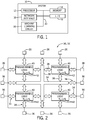
- FIG. 1 illustrates a block diagram of a data processing system 10 that may be used to perform one or more tasks via machine learning.
- the data processing system 10 may include a processor 10 operatively coupled to a memory 14.
- the processor 10 may execute one or more instructions stored on the memory 14 to perform the one or more tasks.
- the data processing system 10 may include a network interface 16 to send and/or receive data via a network to communicate with other electronic devices.
- the data processing system 10 may include one or more inputs/outputs (I/O) 18 that may be used to receive data via I/O devices, such as a keyboard, mouse, display, buttons, or other controls.
- the data processing system 10 may include a machine learning circuit 20 that performs one or more tasks using machine learning methods and techniques.
- the machine learning circuit 20 may include a PLD, such as an FPGA.
- a PLD such as an FPGA.
- Each of the processor 12, the memory 14, the network interface 16, the I/O 18, and the machine learning circuit 20 may be communicatively coupled to one another via interconnection circuitry 22, such as a communication bus.
- FIG. 2 illustrates an IC 30, which may be a programmable logic device, such as a field-programmable gate array (FPGA) 32.
- FPGA field-programmable gate array
- the device is referred to as an IC 30, though it should be understood that the device may be any suitable type of device (e.g., application-specific standard product) may be used.
- IC 30 may have input/output circuitry 34 for driving signals off IC 30 and for receiving signals from other devices via input/output pins 36.
- Interconnection resources 38 such as global and local vertical and horizontal conductive lines and buses, may be used to route signals on IC 30. Additionally, interconnection resources 38 may include fixed interconnects (conductive lines) and programmable interconnects (i.e., programmable connections between respective fixed interconnects). Programmable logic 40 may include combinational and sequential logic circuitry. For example, programmable logic 40 may include look-up tables, registers, and multiplexers. In various embodiments, the programmable logic 40 may be configured to perform a custom logic function. The programmable interconnects associated with interconnection resources may be considered to be a part of programmable logic 40.
- the IC 30 may include programmable elements 42 with the programmable logic 40. The programmable elements 42 may be based on any suitable programmable technology, such as fuses, antifuses, electrically-programmable read-only-memory technology, random-access memory cells, mask-programmed elements, and so forth.
- the circuitry of IC 30 may be organized using any suitable architecture.
- the logic of IC 30 may be organized in a series of rows and columns of larger programmable logic regions, each of which may have multiple smaller logic regions.
- the logic resources of IC 30 may be interconnected by interconnection resources 38 such as associated vertical and horizontal conductors.
- interconnection resources 38 such as associated vertical and horizontal conductors.
- these conductors may include global conductive lines that span substantially all of IC 30, fractional lines such as half-lines or quarter lines that span part of IC 30, staggered lines of a particular length (e.g., sufficient to interconnect several logic areas), smaller local lines, or any other suitable interconnection resource arrangement.
- the logic of IC 30 may be arranged in more levels or layers in which multiple large regions are interconnected to form still larger portions of logic. Still further, other device arrangements may use logic that is not arranged in a manner other than rows and columns.
- the machine learning circuit 20 may perform the one or more tasks using hardware of the IC 30.
- the machine learning circuit 20 may utilize arithmetic logic circuitry to perform arithmetic operations used in machine learning methods and techniques.
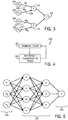
- FIG. 3 is a network diagram of an example of a machine learning network, such as a neural network 100, which may be utilized to perform one or more tasks on the machine learning circuit 20. While the neural network 100 is described in detail as an example, any suitable machine learning methods and techniques may be used.
- the neural network 100 includes a set of inputs 102, 103, 104, and 106, a set of weights 108, 109, 110, and 112, a set of summations 114 and 115, and a resultant value 116.
- Each of the inputs 102, 103, 104, and 106 is weighted with a respective weight to determine a respective weighted value 108, 109, 110, and 112.
- the weighted values 108 and 109 may be summed at the summation 114, and the weighted values 110 and 112 may be summed at the summation 115.
- the resultant value 116 may be output from the summations 114 and 115 and used to perform one or more tasks from prior data. While four inputs and two summations are shown, this is meant to be illustrative and any suitable combination of inputs, weightings, summations, and connections therebetween may be used.
- FIG. 4 is a flow diagram of a process 130 that may be performed in conjunction with the neural network 100 on the IC 30.
- the IC 30 may perform training in which the weighted values 108, 109, 110, and 112 are determined and/or adjusted such that the weights applied to the inputs 102, 103, 104, and 106 indicate a likelihood that the respective inputs 102, 103, 104, and 106 predict the resultant value 116.
- the IC 30 may perform inferences and/or classifications on new data.
- the neural network 100 may be trained using images of shapes (e.g., circles, triangles, squares) in which the shape in the image is known. Then, the IC 30 may classify the shapes of new data using the neural network 100 after the weights have been adjusted from the training data. By adjusting the weights applied to the inputs 102, 103, 104, and 106 based on the training data, weights may be obtained that, when applied to new images, reflect a likelihood that the respective input of the new image includes a certain shape. In some embodiments, continued learning may occur in which new data is then verified and the weights are continually adjusted.
- Each of the blocks 134 may be performed via the machine learning circuit 20 and/or some operations of each of the blocks 134 may be performed via the processor 12.
- FIG. 5 is a network diagram of an example of a neural network 138 having an input layer 140, more than one computational layers 142, and an output layer 144.
- the illustrated embodiment may be referred to as a deep neural network due to having more than one computational layers 142, also referred to as hidden layers.
- each input is weighted and summed at four summations, and each respective summation is then weighted and summed at three summations, which are then used to output a resultant value.
- the circuitry of the IC 30 may further include one or more DSP blocks.
- the DSP block may include one or more (multiply-accumulate) MAC blocks, or MAC circuits.
- Each MAC block may include hardened circuitry (e.g., multiplier circuitry and accumulator circuitry) that is designed and specialized to perform multiplication and accumulation operations. While the MAC block may include circuitry that performs multiplication and accumulation of inputs having a certain amount of precision, the neural network 100 may have inputs 102, 103, 104, and 106 and weights of lower precision than the circuitry of the MAC block.
- the MAC block may include circuitry designed to process eighteen-bit inputs. By combining more than one value from the neural network 100 into the same operand of the MAC block, each multiplication of the MAC block may process additional values associated with the neural network 100 to improve throughput of the neural network 100.
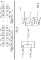
- FIG. 6 is an example of a set of data structures 200 of the IC 30 having combined values in the same operand to allow the IC 30 to process values of the neural network 100 at a faster rate.
- the IC 30 may combine a first value 204 and a second value 206 into a first operand 208. That is, the IC 30 may pack each bit of the first value 204 and each bit of the second value 206 into the first operand 208.
- a first component (e.g., first set of bits) of the first operand 208 may represent a first value 204 and a second component (e.g., second set of bits) of the first operand 208 may represent a second value 206.
- the operand 208 may include a gap between the first value 204 and the second value 206 to prevent overflow.
- the gap 210 may be at least the number of bits of the first value 204 or the second value 206.
- the first value 204 may be the first input 102 and the second value 206 may be the second input 104.
- the IC 30 may combine a third value 212 and a fourth value 214 into a second operand 216.
- the second operand 216 may include a gap 218 between the third value 212 and the fourth value 214 to prevent overflow.
- the gap 218 may be at least the number of bits of the third value 212 or the fourth value 214.
- the first value 204, the second value 206, the third value 212, the fourth value 214, and the gaps 210 and 218 may each be six bits.
- the third value 212 may be a first weight to be applied to the first input 102 and the fourth value 106 may be a second weight applied to the second input 104.
- the IC 30 may perform a multiplication operation on the first operand 208 and the second operand 216 such that a multiplied product 230 includes a first product 232 of the first value 204 multiplied with the third value 212 and a second product 234, from the same multiplication operation, of the second value 206 multiplied with the fourth value 214. That is, by combining or packing more than one value into each operand 208 and 216 with sufficient gap 210 and 218 between the values, the multiplied product 230 may include each respective product without overflow.
- the first product 232 may be the weighted value 108 from the first weight applied to the first input 102 and the second product 234 may be the second weighted value 110 from the second weight applied to the second input 104.
- the resultant value 116 may be determined at a faster rate due to increased throughput.
- Each of the first product 232 and the second product 234 may subsequently be split from the multiplied product 230 and accumulated. Because the accumulation may be a faster operation than the multiplication, the performance of the neural network 100 may be improved by determining more than one product from a single multiplication operation using more of the available precision in the hardened multiplier circuitry of the IC 30. Further, the hardened circuitry of MAC blocks in the IC 30 may be specialized to perform the multiplications to determine the weighted values 108, 109, 110, and 112 at a faster rate than in circuitry that executes multiplications in soft logic due to the specialization of the hardened circuitry.
- FIG. 7 is a block diagram of circuitry of the IC 30 that performs the arithmetic operations described with respect to FIG. 6 .
- the IC 30 may include a DSP block 250 having first input circuitry 252 and second input circuitry 254 to receive a first operand 208 and a second operand 216 respectively.
- the DSP block 250 may include a MAC block 260 having multiplier circuitry 262 that multiplies the first operand 208 with the second operand 216 and outputs a product. That is, the multiplier circuitry 262 may be designed or hardened with circuitry to perform multiplication operations on operands of a certain precision. By including more than one value of lower precision than the designed operand precision into the operand prior to executing the multiplication operation, more than one product may be determined from the multiplication operation.
- the MAC block 260 may include adder circuitry 264 that may add the products from the multiplier circuitry 262. Upon completing the MAC operation, the MAC block 260 may output a result via the output circuitry 268.
- the IC 30 may include more than one DSP block 250 (e.g., 2, 3, 4, 5, or more), and each DSP block may include more than one MAC block 252 (e.g. 2, 3, 4, 5, 10, 20, 50, or more).
- the MAC block 252 may include bypass circuitry 270 (e.g., multiplexor) to bypass the adder 264 and to provide the multiplied product 230 to soft logic 274 of the IC 30. Further, the IC 30 may then perform the summations 114 and 115 of the neural network in the soft logic 274 of the IC 30.
- the soft logic 274 may refer to programmed instructions (e.g., code) stored in memory on the IC 30 to execute operations of the IC 30.
- the IC 30 may be programmed to execute instructions to split the first product 232 and the second product 234 from the multiplied product 230.
- the IC 30 may then execute instructions to accumulate 276 the first product (e.g., first weighted value 108) with one or more other products (e.g., weighted value 109) to determine a total from the summation 114.
- the IC 30 may execute instructions to accumulate 278 the second product (e.g., weighted value 110) with one or more other products (e.g., weighted value 112).
- the first product e.g., weighted value 108 may be held at block 282.
- the IC 30 may then perform another multiplication to determine third and fourth products (e.g., the weighted values 109 and 112) by combining the fifth and sixth values (e.g., inputs 103 and 106) into a third operand and seventh and eighth values (e.g., the weights for the respective inputs) into a fourth operand.
- the third and fourth products (e.g., weighted values 109 and 112) may then be added to each respective total being held 282 and 284.
- the accumulators in soft logic 274, more accumulation operations may be performed with less or no risk of overflow.
- the IC 30 may obtain additional products in each multiplication operation.
- FIG. 8 is a more generalized example of a data structure 300 used in performing multiplication operations in the neural network 100 on the IC 30.
- the IC 30 may combine values A[0] to A[n] into a first operand.
- the IC 30 may combine values B[0] to B[n] into a second operand.
- Each of the values 302 and 306 may be separated from other values 302 and 306 by gaps 304 and 308 to prevent overflow.
- the multiplied product 310 may include a set of multiplied values 312 C[0] to C[n] from multiplying each respective value of A to B.
- Lower precision levels of the neural network may allow for additional values to be included in each multiplication operation.
- the following table may reflect precision levels with respect to the number of values in each operand: Precision (bits) Compute Improvement (Low-precision - 18-bits) 1 9x 2 5x 3 3x 4 2x 5 2x 6 2x
- num comp floor Width Mult 2 ⁇ precision + 0.5
- num comp refers to the number of values that may be included in each operand
- Width Mult refers to the number of bits in each operand
- precision refers to the number of bits used in operations in the neural network 100.
- FIG. 9 is a generalized block diagram of circuitry of the IC 30 that performs arithmetic operations for the neural network of FIG. 3 using the data structure of FIG. 8 .
- the IC 30 includes similar circuitry to the circuitry described with respect to FIG. 7 . Further, additional accumulators (e.g., in code) may be used for each of the values 312 in the multiplied product 310.
- FIG. 10 is a block diagram of another data structure 324 that may be used in conjunction with the circuitry described with respect to FIG. 9 .
- the data structure 324 includes a first operand having N values 326 A[0] to A[n] with gaps 328 between each of the values 326.
- the data structure 324 includes a second operand having a single value B[0] 330 and padding 332 throughout the remainder of the first operand.
- the single value B[0] may be the same precision as each of the N values of the first operand.
- the IC 30 may determine a first multiplied product 334 by multiplying a first value A[0] of the first operand with B[0] 330.
- the IC 30 may determine a second multiplied product 334 by multiplying a second value A[1] of the first operand with B[0] 330. That is, B[0] 330 may be multiplied with each of the N values 326 of the first operand.
- FIG. 11 is a flow diagram of a process 340 performed by the IC 30 to perform the arithmetic operations of the neural network 100 to output a resultant value 116 described in conjunction with the example of FIGS. 5 and 6 .
- the IC 30 may combine (e.g., pack) a first value and a second value into a first operand.
- the IC 30 may combine (e.g., pack) a third value and a fourth value into a second operand.
- additional values may be included in each of the first operand and the second operand. Further, in certain embodiments described with respect to FIG. 10 , the IC 30 may simply have a single value in the second operand.
- the IC 30 may multiply the first operand with the second operand to determine a first multiplied product based at least in part on the first value and a second multiplied product based at least in part on the second value.
- the first multiplied product may be the first value multiplied by the third value and the second multiplied product may be the second value multiplied by the fourth value. In this manner, more than one multiplied products may be determined from the same multiplication operation performed by the hardened multiplier circuitry.
- the multiplication operation may be performed in the hardened multiplier circuitry and the multiplied result having both the first multiplied product and the second multiplied product may be output to soft logic where the first multiplied product and the second multiplied product may be split from one another.
- the IC 30 may perform a correction operation (e.g., in the soft logic) to correct any collisions in the multiplication operation. For example, if the first multiplied product overlaps with the second multiplied product due to overflow, the IC 30 may perform an exclusive OR (XOR) operation, a masking operation, or the like, to correct for the overlapped values.
- the IC 30 may then add the first multiplied product, the second multiplied product, or both, to at least one summation. For example, the first multiplied product and the second multiplied product may be added to the same summation 114, or each product may be added to different summations 114 and 115 respectively.
- the IC 30 may output a resultant value based at least in part on the at least one summation. That is, the resultant value may be from a total of two summations 114 and 115, as in FIG. 3 , or the resultant value may be determined after several computational layers, as in FIG. 5 .
- the resultant value 116 may be output (e.g., via I/O pins 36) to control an operation of the IC 30.
- the resultant value 116 may be displayed to a user.
- the resultant value 116 may be sent to another electronic device.
- the invention may be related to one or more of the following examples:
Landscapes
- Engineering & Computer Science (AREA)
- Physics & Mathematics (AREA)
- Theoretical Computer Science (AREA)
- General Physics & Mathematics (AREA)
- Computing Systems (AREA)
- General Engineering & Computer Science (AREA)
- Computational Mathematics (AREA)
- Mathematical Analysis (AREA)
- Mathematical Optimization (AREA)
- Pure & Applied Mathematics (AREA)
- Biomedical Technology (AREA)
- Life Sciences & Earth Sciences (AREA)
- Health & Medical Sciences (AREA)
- Biophysics (AREA)
- Molecular Biology (AREA)
- Artificial Intelligence (AREA)
- Computational Linguistics (AREA)
- Data Mining & Analysis (AREA)
- Evolutionary Computation (AREA)
- General Health & Medical Sciences (AREA)
- Mathematical Physics (AREA)
- Software Systems (AREA)
- Neurology (AREA)
- Complex Calculations (AREA)
- Logic Circuits (AREA)
- Image Analysis (AREA)
Abstract
Description
- The present disclosure relates generally to efficient utilization of arithmetic circuitry of an integrated circuit, such as multiply-accumulate circuitry and/or digital signal processor (DSP) circuitry, for machine learning.
- This section is intended to introduce the reader to various aspects of art that may be related to various aspects of the present disclosure, which are described and/or claimed below. This discussion is believed to be helpful in providing the reader with background information to facilitate a better understanding of the various aspects of the present disclosure. Accordingly, it may be understood that these statements are to be read in this light, and not as admissions of prior art.
- Integrated circuits, such as field programmable gate arrays (FPGAs), may include circuitry to perform various mathematical operations. For example, a deep learning neural network may be implemented in one or more integrated circuit devices for machine learning applications. The integrated circuit devices may perform several operations to output results for the neural network. However, in some instances, throughput of mathematical operations in neural networks may be limited by the hardware of the integrated circuit. Because of these limitations, the neural network may perform at a rate slower than desired.
- Various aspects of this disclosure may be better understood upon reading the following detailed description and upon reference to the drawings in which:
-
FIG. 1 is a block diagram of a data processing system that performs machine learning via a machine learning circuit, in accordance with an embodiment; -
FIG. 2 is a block diagram of the machine learning circuit ofFIG. 1 , in accordance with an embodiment; -
FIG. 3 is a network diagram of a neural network used to perform a task via the machine learning circuit ofFIG. 1 , in accordance with an embodiment; -
FIG. 4 is a flow diagram of a process performed by the machine learning circuit ofFIG. 1 , in accordance with an embodiment; -
FIG. 5 is diagram of another neural network used to perform a task via the machine learning circuit ofFIG. 1 , in accordance with an embodiment; -
FIG. 6 is a block diagram of a data structure for multiplication operations performed via the machine learning circuit ofFIG. 1 , in accordance with an embodiment; -
FIG. 7 is a block diagram of the machine learning circuit ofFIG. 1 used to perform multiplication operations, in accordance with an embodiment; -
FIG. 8 is a block diagram of a generalized data structure for multiplication operations performed via the machine learning circuit ofFIG. 1 , in accordance with an embodiment; -
FIG. 9 is a block diagram of the machine learning circuit ofFIG. 1 used to perform generalized multiplication operations, in accordance with an embodiment; -
FIG. 10 is a block diagram of another data structure for multiplication operations performed via the machine learning circuit ofFIG. 1 , in accordance with an embodiment; and -
FIG. 11 is a flow diagram of a process performed by the machine learning circuit ofFIG. 1 to perform multiplication operations for neural networks, in accordance with an embodiment. - One or more specific embodiments will be described below. In an effort to provide a concise description of these embodiments, not all features of an actual implementation are described in the specification. It may be appreciated that in the development of any such actual implementation, as in any engineering or design project, numerous implementation-specific decisions must be made to achieve the developers' specific goals, such as compliance with system-related and business-related constraints, which may vary from one implementation to another. Moreover, it may be appreciated that such a development effort might be complex and time consuming, but would nevertheless be a routine undertaking of design, fabrication, and manufacture for those of ordinary skill having the benefit of this disclosure.
- Machine learning is used in a variety of settings to perform tasks through the use of examples. For example, neural networks may be used to perform a task without task-specific programming. That is, neural networks may be trained from prior data to classify or infer information from current data. For instance, training data may be used to identify images that contain an object by analyzing other images that include and do not include the object. While images are used as an example, this is simply meant to be illustrative and any suitable neural network task may be performed in the embodiments described below.
- Configurable devices, such as programmable logic devices (PLDs), may perform one or more operations to execute tasks via machine learning. For example, integrated circuits (ICs), such as field programmable gate arrays (FPGAs), may include one or more digital signal processing (DSP) blocks, or DSP circuits, having one or more specialized processing blocks to perform arithmetic operations on data received by the DSP block. One type of specialized processing blocks in the DSP block may be multiply-accumulate (MAC) blocks, or MAC circuits, that include one or more multiplier circuits and/or one or more accumulator circuits. For instance, in some FPGAs, the MAC blocks may be hardened intellectual property (IP) blocks having specialized multiply circuitry coupled to specialized adder circuitry. Examples of operations performed by the MAC blocks include dot products, vector multiplications, and the like. As described below, the one or more multipliers of the DSP blocks may be used to perform neural network arithmetic operations during the classification or inference stage. However, throughput of the digital signal processor (DSP) may be limited by hardware of the IC. For example, the number of MAC blocks may limit the performance (e.g., speed) of the IC in performing arithmetic operations of the neural network.
- Some arithmetic operations in neural networks may not involve the same precision as the precision designed to be processed in the MAC blocks. For example, the MAC block may include circuitry that processes 18 bit operands, but the neural network may involve multiplying lower precision 6 bit operands. The systems and methods described below improve neural network performances in ICs by better utilizing capacity of operands in multiply operations. By combining more than one quantity into each operand of multiply operations, speed of performing MAC operations (e.g., weightings and summations) by MAC blocks of ICs in the neural network applications may be improved. For example, two or more quantities may be packed into a first operand that is received by multiplier circuitry. Two or more quantities may be packed into a second operand received by the multiplier circuitry. The multiplier circuitry may then perform the multiplication operation between the first operand and the second operand to determine a product between each of the respective quantities. The multiplier circuitry may then output each of the products to be accumulated. To prevent overflow from the multiplication, a gap may be included between each of the quantities combined in the operands.
- Further, to reduce likelihood of overflow from the accumulation, accumulator circuitry of the MAC block may be bypassed to a soft logic accumulator. That is, the multiplication of the MAC operation may be performed in a hardened multiplier that is specialized at performing multiplications and accumulations, and the accumulation of the MAC operation may be performed in soft logic to prevent overflow due to accumulating several products output from the multiplication.
- With the foregoing in mind,
FIG. 1 illustrates a block diagram of adata processing system 10 that may be used to perform one or more tasks via machine learning. Thedata processing system 10 may include aprocessor 10 operatively coupled to amemory 14. Theprocessor 10 may execute one or more instructions stored on thememory 14 to perform the one or more tasks. Thedata processing system 10 may include anetwork interface 16 to send and/or receive data via a network to communicate with other electronic devices. Thedata processing system 10 may include one or more inputs/outputs (I/O) 18 that may be used to receive data via I/O devices, such as a keyboard, mouse, display, buttons, or other controls. Thedata processing system 10 may include amachine learning circuit 20 that performs one or more tasks using machine learning methods and techniques. Themachine learning circuit 20 may include a PLD, such as an FPGA. Each of theprocessor 12, thememory 14, thenetwork interface 16, the I/O 18, and themachine learning circuit 20 may be communicatively coupled to one another viainterconnection circuitry 22, such as a communication bus. - The hardware of the
machine learning circuit 20 may perform one or more tasks using neural networks 100 and 138. Turning now to a more detailed discussion of an example of themachine learning circuit 20,FIG. 2 illustrates an IC 30, which may be a programmable logic device, such as a field-programmable gate array (FPGA) 32. For the purposes of this example, the device is referred to as an IC 30, though it should be understood that the device may be any suitable type of device (e.g., application-specific standard product) may be used. As shown, IC 30 may have input/output circuitry 34 for driving signals off IC 30 and for receiving signals from other devices via input/output pins 36.Interconnection resources 38, such as global and local vertical and horizontal conductive lines and buses, may be used to route signals on IC 30. Additionally,interconnection resources 38 may include fixed interconnects (conductive lines) and programmable interconnects (i.e., programmable connections between respective fixed interconnects).Programmable logic 40 may include combinational and sequential logic circuitry. For example,programmable logic 40 may include look-up tables, registers, and multiplexers. In various embodiments, theprogrammable logic 40 may be configured to perform a custom logic function. The programmable interconnects associated with interconnection resources may be considered to be a part ofprogrammable logic 40. The IC 30 may includeprogrammable elements 42 with theprogrammable logic 40. Theprogrammable elements 42 may be based on any suitable programmable technology, such as fuses, antifuses, electrically-programmable read-only-memory technology, random-access memory cells, mask-programmed elements, and so forth. - The circuitry of IC 30 may be organized using any suitable architecture. As an example, the logic of IC 30 may be organized in a series of rows and columns of larger programmable logic regions, each of which may have multiple smaller logic regions. The logic resources of IC 30 may be interconnected by
interconnection resources 38 such as associated vertical and horizontal conductors. For example, in some embodiments, these conductors may include global conductive lines that span substantially all of IC 30, fractional lines such as half-lines or quarter lines that span part of IC 30, staggered lines of a particular length (e.g., sufficient to interconnect several logic areas), smaller local lines, or any other suitable interconnection resource arrangement. Moreover, in further embodiments, the logic of IC 30 may be arranged in more levels or layers in which multiple large regions are interconnected to form still larger portions of logic. Still further, other device arrangements may use logic that is not arranged in a manner other than rows and columns. As explained below, themachine learning circuit 20 may perform the one or more tasks using hardware of the IC 30. For example, themachine learning circuit 20 may utilize arithmetic logic circuitry to perform arithmetic operations used in machine learning methods and techniques. -
FIG. 3 is a network diagram of an example of a machine learning network, such as a neural network 100, which may be utilized to perform one or more tasks on themachine learning circuit 20. While the neural network 100 is described in detail as an example, any suitable machine learning methods and techniques may be used. The neural network 100 includes a set ofinputs weights summations 114 and 115, and aresultant value 116. Each of theinputs weighted value weighted values 108 and 109 may be summed at the summation 114, and theweighted values summation 115. Theresultant value 116 may be output from thesummations 114 and 115 and used to perform one or more tasks from prior data. While four inputs and two summations are shown, this is meant to be illustrative and any suitable combination of inputs, weightings, summations, and connections therebetween may be used. -
FIG. 4 is a flow diagram of aprocess 130 that may be performed in conjunction with the neural network 100 on the IC 30. Atblock 132, the IC 30 may perform training in which theweighted values inputs respective inputs resultant value 116. - Upon training the neural network 100, at
block 134, the IC 30 may perform inferences and/or classifications on new data. In an example involving image recognition, for example, the neural network 100 may be trained using images of shapes (e.g., circles, triangles, squares) in which the shape in the image is known. Then, the IC 30 may classify the shapes of new data using the neural network 100 after the weights have been adjusted from the training data. By adjusting the weights applied to theinputs blocks 134 may be performed via themachine learning circuit 20 and/or some operations of each of theblocks 134 may be performed via theprocessor 12. -
FIG. 5 is a network diagram of an example of a neural network 138 having aninput layer 140, more than onecomputational layers 142, and anoutput layer 144. The illustrated embodiment may be referred to as a deep neural network due to having more than onecomputational layers 142, also referred to as hidden layers. As the number ofcomputational layers 142 increases, the complexity and processing of inputs increases. In the illustrated embodiment, each input is weighted and summed at four summations, and each respective summation is then weighted and summed at three summations, which are then used to output a resultant value. - As explained below the circuitry of the IC 30 may further include one or more DSP blocks. The DSP block may include one or more (multiply-accumulate) MAC blocks, or MAC circuits. Each MAC block may include hardened circuitry (e.g., multiplier circuitry and accumulator circuitry) that is designed and specialized to perform multiplication and accumulation operations. While the MAC block may include circuitry that performs multiplication and accumulation of inputs having a certain amount of precision, the neural network 100 may have
inputs inputs -
FIG. 6 is an example of a set ofdata structures 200 of the IC 30 having combined values in the same operand to allow the IC 30 to process values of the neural network 100 at a faster rate. The IC 30 may combine afirst value 204 and asecond value 206 into afirst operand 208. That is, the IC 30 may pack each bit of thefirst value 204 and each bit of thesecond value 206 into thefirst operand 208. For example, a first component (e.g., first set of bits) of thefirst operand 208 may represent afirst value 204 and a second component (e.g., second set of bits) of thefirst operand 208 may represent asecond value 206. Further, theoperand 208 may include a gap between thefirst value 204 and thesecond value 206 to prevent overflow. For example, thegap 210 may be at least the number of bits of thefirst value 204 or thesecond value 206. Thefirst value 204 may be thefirst input 102 and thesecond value 206 may be thesecond input 104. - Similarly, the IC 30 may combine a
third value 212 and afourth value 214 into asecond operand 216. Thesecond operand 216 may include agap 218 between thethird value 212 and thefourth value 214 to prevent overflow. Thegap 218 may be at least the number of bits of thethird value 212 or thefourth value 214. In the example described above in which the neural network 100 utilizes six-bit precision, thefirst value 204, thesecond value 206, thethird value 212, thefourth value 214, and thegaps third value 212 may be a first weight to be applied to thefirst input 102 and thefourth value 106 may be a second weight applied to thesecond input 104. - The IC 30 may perform a multiplication operation on the
first operand 208 and thesecond operand 216 such that a multipliedproduct 230 includes afirst product 232 of thefirst value 204 multiplied with thethird value 212 and asecond product 234, from the same multiplication operation, of thesecond value 206 multiplied with thefourth value 214. That is, by combining or packing more than one value into eachoperand sufficient gap product 230 may include each respective product without overflow. For example, in the neural network 100, thefirst product 232 may be the weighted value 108 from the first weight applied to thefirst input 102 and thesecond product 234 may be the secondweighted value 110 from the second weight applied to thesecond input 104. By combining the values from the neural network 100 into eachoperand resultant value 116 may be determined at a faster rate due to increased throughput. - Each of the
first product 232 and thesecond product 234 may subsequently be split from the multipliedproduct 230 and accumulated. Because the accumulation may be a faster operation than the multiplication, the performance of the neural network 100 may be improved by determining more than one product from a single multiplication operation using more of the available precision in the hardened multiplier circuitry of the IC 30. Further, the hardened circuitry of MAC blocks in the IC 30 may be specialized to perform the multiplications to determine theweighted values -
FIG. 7 is a block diagram of circuitry of the IC 30 that performs the arithmetic operations described with respect toFIG. 6 . The IC 30 may include aDSP block 250 havingfirst input circuitry 252 andsecond input circuitry 254 to receive afirst operand 208 and asecond operand 216 respectively. TheDSP block 250 may include aMAC block 260 havingmultiplier circuitry 262 that multiplies thefirst operand 208 with thesecond operand 216 and outputs a product. That is, themultiplier circuitry 262 may be designed or hardened with circuitry to perform multiplication operations on operands of a certain precision. By including more than one value of lower precision than the designed operand precision into the operand prior to executing the multiplication operation, more than one product may be determined from the multiplication operation. - In some embodiments, the MAC block 260 may include
adder circuitry 264 that may add the products from themultiplier circuitry 262. Upon completing the MAC operation, the MAC block 260 may output a result via theoutput circuitry 268. In the illustrated embodiment, the IC 30 may include more than one DSP block 250 (e.g., 2, 3, 4, 5, or more), and each DSP block may include more than one MAC block 252 (e.g. 2, 3, 4, 5, 10, 20, 50, or more). - The
MAC block 252 may include bypass circuitry 270 (e.g., multiplexor) to bypass theadder 264 and to provide the multipliedproduct 230 tosoft logic 274 of the IC 30. Further, the IC 30 may then perform thesummations 114 and 115 of the neural network in thesoft logic 274 of the IC 30. Thesoft logic 274 may refer to programmed instructions (e.g., code) stored in memory on the IC 30 to execute operations of the IC 30. The IC 30 may be programmed to execute instructions to split thefirst product 232 and thesecond product 234 from the multipliedproduct 230. The IC 30 may then execute instructions to accumulate 276 the first product (e.g., first weighted value 108) with one or more other products (e.g., weighted value 109) to determine a total from the summation 114. The IC 30 may execute instructions to accumulate 278 the second product (e.g., weighted value 110) with one or more other products (e.g., weighted value 112). For example, the first product (e.g., weighted value 108) may be held atblock 282. The IC 30 may then perform another multiplication to determine third and fourth products (e.g., theweighted values 109 and 112) by combining the fifth and sixth values (e.g.,inputs 103 and 106) into a third operand and seventh and eighth values (e.g., the weights for the respective inputs) into a fourth operand. The third and fourth products (e.g.,weighted values 109 and 112) may then be added to each respective total being held 282 and 284. By implementing the accumulators insoft logic 274, more accumulation operations may be performed with less or no risk of overflow. By moving to lower precision neural networks than the six bit example, the IC 30 may obtain additional products in each multiplication operation. -
FIG. 8 is a more generalized example of adata structure 300 used in performing multiplication operations in the neural network 100 on the IC 30. The IC 30 may combine values A[0] to A[n] into a first operand. Similarly, the IC 30 may combine values B[0] to B[n] into a second operand. Each of thevalues other values gaps - Upon performing the multiplication operation, the multiplied
product 310 may include a set of multiplied values 312 C[0] to C[n] from multiplying each respective value of A to B. Lower precision levels of the neural network may allow for additional values to be included in each multiplication operation. For example in an eighteen bit multiplication operation the following table may reflect precision levels with respect to the number of values in each operand:Precision (bits) Compute Improvement (Low-precision - 18-bits) 1 9x 2 5x 3 3x 4 2x 5 2x 6 2x - This relationship may be more generalized according to the following equation:

-
FIG. 9 is a generalized block diagram of circuitry of the IC 30 that performs arithmetic operations for the neural network ofFIG. 3 using the data structure ofFIG. 8 . The IC 30 includes similar circuitry to the circuitry described with respect toFIG. 7 . Further, additional accumulators (e.g., in code) may be used for each of thevalues 312 in the multipliedproduct 310. -
FIG. 10 is a block diagram of anotherdata structure 324 that may be used in conjunction with the circuitry described with respect toFIG. 9 . Thedata structure 324 includes a first operand having N values 326 A[0] to A[n] withgaps 328 between each of thevalues 326. Thedata structure 324 includes a second operand having a single value B[0] 330 andpadding 332 throughout the remainder of the first operand. The single value B[0] may be the same precision as each of the N values of the first operand. Upon performing the multiplication operation, the IC 30 may determine a first multipliedproduct 334 by multiplying a first value A[0] of the first operand with B[0] 330. The IC 30 may determine a second multipliedproduct 334 by multiplying a second value A[1] of the first operand with B[0] 330. That is, B[0] 330 may be multiplied with each of the N values 326 of the first operand. -
FIG. 11 is a flow diagram of aprocess 340 performed by the IC 30 to perform the arithmetic operations of the neural network 100 to output aresultant value 116 described in conjunction with the example ofFIGS. 5 and6 . Atblock 342, the IC 30 may combine (e.g., pack) a first value and a second value into a first operand. In some embodiments, the IC 30 may combine (e.g., pack) a third value and a fourth value into a second operand. As mentioned above with respect toFIGS. 8 and 9 , additional values may be included in each of the first operand and the second operand. Further, in certain embodiments described with respect toFIG. 10 , the IC 30 may simply have a single value in the second operand. Atblock 344, the IC 30 may multiply the first operand with the second operand to determine a first multiplied product based at least in part on the first value and a second multiplied product based at least in part on the second value. In the example in which the second operand includes a third value and a fourth value, for instance, the first multiplied product may be the first value multiplied by the third value and the second multiplied product may be the second value multiplied by the fourth value. In this manner, more than one multiplied products may be determined from the same multiplication operation performed by the hardened multiplier circuitry. In some embodiments, the multiplication operation may be performed in the hardened multiplier circuitry and the multiplied result having both the first multiplied product and the second multiplied product may be output to soft logic where the first multiplied product and the second multiplied product may be split from one another. - In some embodiments, at
block 346, the IC 30 may perform a correction operation (e.g., in the soft logic) to correct any collisions in the multiplication operation. For example, if the first multiplied product overlaps with the second multiplied product due to overflow, the IC 30 may perform an exclusive OR (XOR) operation, a masking operation, or the like, to correct for the overlapped values. Atblock 348, the IC 30 may then add the first multiplied product, the second multiplied product, or both, to at least one summation. For example, the first multiplied product and the second multiplied product may be added to the same summation 114, or each product may be added todifferent summations 114 and 115 respectively. Atblock 350, the IC 30 may output a resultant value based at least in part on the at least one summation. That is, the resultant value may be from a total of twosummations 114 and 115, as inFIG. 3 , or the resultant value may be determined after several computational layers, as inFIG. 5 . Theresultant value 116 may be output (e.g., via I/O pins 36) to control an operation of the IC 30. In some embodiments, theresultant value 116 may be displayed to a user. In other embodiments, theresultant value 116 may be sent to another electronic device. By combining lower precision values into operands having a designed precision greater than the lower precision values, throughput through the neural network may be improved. - While the embodiments set forth in the present disclosure may be susceptible to various modifications and alternative forms, specific embodiments have been shown by way of example in the drawings and have been described in detail herein. However, it may be understood that the disclosure is not intended to be limited to the particular forms disclosed. The disclosure is to cover all modifications, equivalents, and alternatives falling within the spirit and scope of the disclosure as defined by the following appended claims.
- The invention may be related to one or more of the following examples:
- 1. An integrated circuit device comprising:
- first input circuitry to a hardened multiplier, wherein the first input circuitry is configured to receive a first operand, wherein a first component of the first operand comprises a first value and a second component of the first operand comprises a second value;
- second input circuitry to the hardened multiplier, wherein the second input circuitry is configured to receive a second operand, wherein a first component of the second operand includes a third value;
- multiplication circuitry of the hardened multiplier, wherein the multiplication circuitry is configured to multiply the first operand and the second operand in a single multiply operation to produce a product that contains a plurality of results equivalent to a corresponding plurality of distinct multiply operations, wherein the product comprises a first component that contains a first result of the plurality of results, wherein the first result is equivalent to a first multiply operation based on the first value, and wherein the product comprises a second component that contains a second result of the plurality of results, wherein the second result is equivalent to a second multiply operation based on the second value.
- 2. The system of example 1, wherein the integrated circuit device comprises soft logic circuitry configured to determine a first accumulated value based at least in part on the first result and a second accumulated value based at least in part on the second result.
- 3. The system of any of the preceding examples, wherein the multiplier circuitry is configured to perform the multiplication operation via digital signal processing (DSP) circuitry.
- 4. The system of any of the preceding examples, wherein the first value and the second value each have a lower precision than a precision of the first operand and the second operand.
- 5. The system of any of the preceding examples, wherein the first value has a single bit of precision.
- 6. The system of any of the preceding examples, wherein the first result comprises a weighted value of a neural network, wherein the first value comprises an input into the neural network and the third value comprises a weight of the neural network.
- 7. The system of any of the preceding examples, comprising bypass circuitry configured to bypass hardened adder circuitry of the integrated circuit device.
- 8. The system of any of the preceding examples, wherein the first operand comprises a gap between the first value and the second value to prevent or reduce overflow in the first multiplied value or the second multiplied value.
- 9. The system of any of the preceding examples, wherein the integrated circuit device is configured to perform a correction operation to correct any collisions caused by the multiplication operation, wherein the correction operation comprises an exclusive OR (XOR) operation, a masking operation, or any combination thereof.
- 10. A method for performing arithmetic operations of a neural network on an integrated circuit (IC), comprising:
- packing, via the IC, a first value and a second value into a first operand;
- packing, via the IC, a third value and a fourth value into a second operand;
- performing, via the IC, a multiplication operation of the neural network on the first operand and the second operand such that a first multiplied product comprises the first value multiplied with the third value and a second multiplied product comprises the second value multiplied with the fourth value;
- adding, via the IC, the first multiplied product, the second multiplied product, or both, to at least one summation; and
- outputting, via the IC, a resultant value based at least in part on the at least one summation.
- 11. The method of example 10, wherein the first multiplied product comprises a weighted value from multiplying a first input of the neural network with a weight of the neural network, wherein the first input of the neural network comprises the first value and wherein the weight of the neural network comprises the third value.
- 12. The method of examples 10 or 11, comprising summing the first multiplied product in a computational layer of the neural network.
- 13. The method of any of examples 10-12, comprising outputting a resultant value of the neural network based at least in part on a first summation from the first multiplied product and a second summation from the second multiplied product.
- 14. The method of any of examples 10-13, comprising splitting the first multiplied product from the second multiplied product via soft logic circuitry of the IC.
- 15. The method of any of examples 10-14, comprising:
- receiving the first multiplied product and the second multiplied product at soft logic circuitry of the IC;
- determining a first accumulated value based at least in part on the first multiplied product;
- determining a second accumulated value based at least in part on the second multiplied product;
- outputting a resultant value based at least in part on the first accumulated value and the second accumulated value.
Claims (15)
- An integrated circuit device comprising:programmable logic circuitry;multiplier circuitry;first input circuitry to the multiplier circuitry, wherein the first input circuitry is configurable to receive a first operand, wherein a first component of the first operand comprises a first value, a second component of the first operand comprises a second value, and a third component of the first operand comprises a third value; andsecond input circuitry to the multiplier circuitry, wherein the second input circuitry is configurable to receive a second operand, wherein a first component of the second operand comprises a fourth value, a second component of the second operand comprises a fifth value, and a third component of the second operand comprises a sixth value, wherein the multiplier circuitry is configurable to multiply the first operand and the second operand to produce a plurality of results corresponding to a plurality of distinct multiply operations, wherein the plurality of results comprises:a first result of the plurality of results, wherein the first result is equivalent to a first multiply operation based on the first value and the fourth value;a second result of the plurality of results, wherein the second result is equivalent to a second multiply operation based on the second value and the fifth value; anda third result of the plurality of results, wherein the third result is equivalent to a third multiply operation based on the third value and the sixth value.
- The integrated circuit device of claim 1, wherein the integrated circuit device further comprises accumulator circuitry, wherein the accumulator circuitry is configurable to perform an accumulation of the plurality of results.
- The integrated circuit device of claim 1 or 2, wherein the integrated circuit device comprises a digital processing block comprising the multiplier circuitry, the first input circuitry, and the second input circuitry.
- The integrated circuit device according to any one of claims 1 to 3, wherein the integrated circuit device comprises adder circuitry.
- The integrated circuit device of claim 4, wherein the adder circuitry is configurable to receive one or more inputs comprising at least the first result, the second result, and the third result.
- The integrated circuit device according to any one of claims 1 to 5, wherein the first value, the second value, and the third value each have a precision of at least 6 bits and less than 18 bits.
- The integrated circuit device according to any one of claims 1 to 6, wherein the integrated circuit device is configurable to perform arithmetic operations in a mode optimized for neural network processing.
- The integrated circuit device according to any one of claims 1 to 7, wherein the first component and the second component are received from the programmable logic circuitry.
- A data processing system comprising the integrated circuit device according to any one of claims 1 to 8.
- The data processing system of claim 9, comprising:a processor; anda memory coupled to the processor; anda network interface coupled to the memory and the processor, wherein the network interface is communicatively coupled to a programmable logic device outside of the integrated circuit device.
- A method comprising:receiving, via a first input circuitry, a first component of a first operand that comprises a first value, a second component of the first operand that comprises a second value, and a third component of the first operand that comprises a third value;receiving, via a second input circuitry, a first component of a second operand that comprises a fourth value, a second component of the second operand that comprises a fifth value, and a third component of the second operand comprises a sixth value;multiplying the first operand and the second operand to produce a plurality of results corresponding to a plurality of distinct multiply operations, wherein the plurality of results comprises:a first result of the plurality of results, wherein the first result is equivalent to a first multiply operation based on the first value and the fourth value;a second result of the plurality of results, wherein the second result is equivalent to a second multiply operation based on the second value and the fifth value; anda third result of the plurality of results, wherein the third result is equivalent to a third multiply operation based on the third value and the sixth value.
- The method of claim 11, wherein the first value, the second value, and the third value each have a precision of at least 6 bits and less than 18 bits.
- The method of claims 11 or 12, wherein the first component and the second component are received from a programmable logic fabric.
- The method of according to any one of claims 11 to 13, wherein adder circuitry is configurable to receive one or more inputs comprising at least the first result, the second result, and the third result.
- The method of according to any one of claims 11 to 14, comprising performing arithmetic operations in a mode optimized for neural network processing.
Applications Claiming Priority (3)
| Application Number | Priority Date | Filing Date | Title |
|---|---|---|---|
| US201762488636P | 2017-04-21 | 2017-04-21 | |
| US15/855,604 US11416736B2 (en) | 2017-04-21 | 2017-12-27 | Dense digital arithmetic circuitry utilization for fixed-point machine learning |
| EP18163736.4A EP3392760B1 (en) | 2017-04-21 | 2018-03-23 | Dense digital arithmetic circuitry utilization for fixed-point machine learning |
Related Parent Applications (1)
| Application Number | Title | Priority Date | Filing Date |
|---|---|---|---|
| EP18163736.4A Division EP3392760B1 (en) | 2017-04-21 | 2018-03-23 | Dense digital arithmetic circuitry utilization for fixed-point machine learning |
Publications (2)
| Publication Number | Publication Date |
|---|---|
| EP3869326A1 true EP3869326A1 (en) | 2021-08-25 |
| EP3869326B1 EP3869326B1 (en) | 2024-10-30 |
Family
ID=61952516
Family Applications (2)
| Application Number | Title | Priority Date | Filing Date |
|---|---|---|---|
| EP21168954.2A Active EP3869326B1 (en) | 2017-04-21 | 2018-03-23 | Dense digital arithmetic circuitry utilization for fixed-point machine learning |
| EP18163736.4A Active EP3392760B1 (en) | 2017-04-21 | 2018-03-23 | Dense digital arithmetic circuitry utilization for fixed-point machine learning |
Family Applications After (1)
| Application Number | Title | Priority Date | Filing Date |
|---|---|---|---|
| EP18163736.4A Active EP3392760B1 (en) | 2017-04-21 | 2018-03-23 | Dense digital arithmetic circuitry utilization for fixed-point machine learning |
Country Status (3)
| Country | Link |
|---|---|
| US (1) | US11416736B2 (en) |
| EP (2) | EP3869326B1 (en) |
| CN (3) | CN108734282B (en) |
Families Citing this family (2)
| Publication number | Priority date | Publication date | Assignee | Title |
|---|---|---|---|---|
| US20230161557A1 (en) * | 2021-11-24 | 2023-05-25 | Taiwan Semiconductor Manufacturing Company, Ltd. | Compute-in-memory devices and methods of operating the same |
| US12165041B2 (en) * | 2022-06-09 | 2024-12-10 | Recogni Inc. | Low power hardware architecture for handling accumulation overflows in a convolution operation |
Family Cites Families (10)
| Publication number | Priority date | Publication date | Assignee | Title |
|---|---|---|---|---|
| CN1570843A (en) * | 2003-07-15 | 2005-01-26 | 中国科学院微电子中心 | Circuit realization structure for concurrent low power dissipation software computing element |
| US7702978B2 (en) * | 2006-04-21 | 2010-04-20 | Altera Corporation | Soft error location and sensitivity detection for programmable devices |
| US7720901B1 (en) * | 2006-05-26 | 2010-05-18 | Altera Corporation | Multiplier operable to perform a variety of operations |
| US20090113174A1 (en) * | 2007-10-31 | 2009-04-30 | Texas Instruments Incorporated | Sign Operation Instructions and Circuitry |
| US8533250B1 (en) * | 2009-06-17 | 2013-09-10 | Altera Corporation | Multiplier with built-in accumulator |
| US20120215825A1 (en) * | 2011-02-22 | 2012-08-23 | Mavalankar Abhay M | Efficient multiplication techniques |
| US8996601B2 (en) * | 2012-06-21 | 2015-03-31 | Advanced Micro Devices, Inc. | Method and apparatus for multiply instructions in data processors |
| US9753695B2 (en) * | 2012-09-04 | 2017-09-05 | Analog Devices Global | Datapath circuit for digital signal processors |
| US10310768B1 (en) * | 2017-01-11 | 2019-06-04 | Ambarella, Inc. | Convolution calculations in multiple dimensions |
| US10409887B1 (en) * | 2017-02-28 | 2019-09-10 | Ambarella, Inc. | Generalized dot product for computer vision applications |
-
2017
- 2017-12-27 US US15/855,604 patent/US11416736B2/en active Active
-
2018
- 2018-03-21 CN CN201810233635.4A patent/CN108734282B/en active Active
- 2018-03-21 CN CN202111331751.8A patent/CN113988285B/en active Active
- 2018-03-21 CN CN202511059376.4A patent/CN120952076A/en active Pending
- 2018-03-23 EP EP21168954.2A patent/EP3869326B1/en active Active
- 2018-03-23 EP EP18163736.4A patent/EP3392760B1/en active Active
Non-Patent Citations (5)
| Title |
|---|
| NURVITADHI ERIKO ET AL: "Accelerating Binarized Neural Networks: Comparison of FPGA, CPU, GPU, and ASIC", 2016 INTERNATIONAL CONFERENCE ON FIELD-PROGRAMMABLE TECHNOLOGY (FPT), IEEE, 7 December 2016 (2016-12-07), pages 77 - 84, XP033098828, DOI: 10.1109/FPT.2016.7929192 * |
| TIMILSINA DIWAS: "Faux Vector Processor Design Using FPGA-Based Cores", 22 March 2016 (2016-03-22), XP055818606, Retrieved from the Internet <URL:http://cs.williams.edu/~bailey/Tm16.pdf> [retrieved on 20210628] * |
| UG579: "UltraScale Architecture DSP Slice Advance Specification User Guide", 15 July 2014 (2014-07-15), XP055501401, Retrieved from the Internet <URL:http://citeseerx.ist.psu.edu/viewdoc/download?doi=10.1.1.433.3568&rep=rep1&type=pdf> * |
| YAO FU ET AL: "Embedded Vision with INT8 Optimization on Xilinx Devices", XILINX WHITE PAPER, 19 April 2017 (2017-04-19), XP055501333, Retrieved from the Internet <URL:https://www.xilinx.com/support/documentation/white_papers/wp490-embedded-vision-int8.pdf> [retrieved on 20180822] * |
| ZHANG PEI ET AL: "978-1-4673-9406-2/15/$31.00 c IEEE A Software Configurable and Parallelized Coprocessor Architecture for LQR Control", 1 January 2015 (2015-01-01), XP055818617, Retrieved from the Internet <URL:https://www.ece.iastate.edu/~zambreno/pdf/ZhaMil15A.pdf> [retrieved on 20210628] * |
Also Published As
| Publication number | Publication date |
|---|---|
| CN113988285A (en) | 2022-01-28 |
| US11416736B2 (en) | 2022-08-16 |
| EP3869326B1 (en) | 2024-10-30 |
| CN120952076A (en) | 2025-11-14 |
| EP3392760B1 (en) | 2021-04-21 |
| CN108734282A (en) | 2018-11-02 |
| US20180307975A1 (en) | 2018-10-25 |
| CN108734282B (en) | 2025-08-22 |
| EP3392760A1 (en) | 2018-10-24 |
| CN113988285B (en) | 2025-05-30 |
Similar Documents
| Publication | Publication Date | Title |
|---|---|---|
| US12455722B2 (en) | Floating-point decomposition circuitry with dynamic precision | |
| US11662979B2 (en) | Adder circuitry for very large integers | |
| US12056461B2 (en) | Integrated circuits with machine learning extensions | |
| US12405804B2 (en) | Hardware unit for performing matrix multiplication with clock gating | |
| US9778905B1 (en) | Multiplier circuits configurable for real or complex operation | |
| US10049082B2 (en) | Dot product based processing elements | |
| US10489116B1 (en) | Programmable integrated circuits with multiplexer and register pipelining circuitry | |
| CN112204517B (en) | Multi-input floating point adder | |
| EP3392760B1 (en) | Dense digital arithmetic circuitry utilization for fixed-point machine learning | |
| CN111800124B (en) | Digital signal processing block | |
| Yamamoto et al. | A systematic methodology for design and analysis of approximate array multipliers | |
| US11163530B2 (en) | Programmable-logic-directed multiplier mapping | |
| US10083007B2 (en) | Fast filtering | |
| US8572153B1 (en) | Multiplier circuit configurable for real or complex operation | |
| US7765249B1 (en) | Use of hybrid interconnect/logic circuits for multiplication | |
| US20230128025A1 (en) | Systems and methods for decomposed digital filter | |
| US11768663B1 (en) | Compaction of multiplier and adder circuits | |
| US20250021305A1 (en) | Filtering with Tensor Structures | |
| US20250013431A1 (en) | Modular Multipliers using Hybrid Reduction Techniques | |
| JPH09190338A (en) | Elimination of mathematical overflow flag generation delay in logic unit | |
| US20070239811A1 (en) | Multiplication by one from a set of constants using simple circuitry |
Legal Events
| Date | Code | Title | Description |
|---|---|---|---|
| PUAI | Public reference made under article 153(3) epc to a published international application that has entered the european phase |
Free format text: ORIGINAL CODE: 0009012 |
|
| STAA | Information on the status of an ep patent application or granted ep patent |
Free format text: STATUS: THE APPLICATION HAS BEEN PUBLISHED |
|
| AC | Divisional application: reference to earlier application |
Ref document number: 3392760 Country of ref document: EP Kind code of ref document: P |
|
| AK | Designated contracting states |
Kind code of ref document: A1 Designated state(s): AL AT BE BG CH CY CZ DE DK EE ES FI FR GB GR HR HU IE IS IT LI LT LU LV MC MK MT NL NO PL PT RO RS SE SI SK SM TR |
|
| STAA | Information on the status of an ep patent application or granted ep patent |
Free format text: STATUS: REQUEST FOR EXAMINATION WAS MADE |
|
| 17P | Request for examination filed |
Effective date: 20220215 |
|
| RBV | Designated contracting states (corrected) |
Designated state(s): AL AT BE BG CH CY CZ DE DK EE ES FI FR GB GR HR HU IE IS IT LI LT LU LV MC MK MT NL NO PL PT RO RS SE SI SK SM TR |
|
| STAA | Information on the status of an ep patent application or granted ep patent |
Free format text: STATUS: EXAMINATION IS IN PROGRESS |
|
| 17Q | First examination report despatched |
Effective date: 20230421 |
|
| GRAP | Despatch of communication of intention to grant a patent |
Free format text: ORIGINAL CODE: EPIDOSNIGR1 |
|
| STAA | Information on the status of an ep patent application or granted ep patent |
Free format text: STATUS: GRANT OF PATENT IS INTENDED |
|
| INTG | Intention to grant announced |
Effective date: 20231218 |
|
| GRAJ | Information related to disapproval of communication of intention to grant by the applicant or resumption of examination proceedings by the epo deleted |
Free format text: ORIGINAL CODE: EPIDOSDIGR1 |
|
| STAA | Information on the status of an ep patent application or granted ep patent |
Free format text: STATUS: EXAMINATION IS IN PROGRESS |
|
| GRAP | Despatch of communication of intention to grant a patent |
Free format text: ORIGINAL CODE: EPIDOSNIGR1 |
|
| STAA | Information on the status of an ep patent application or granted ep patent |
Free format text: STATUS: GRANT OF PATENT IS INTENDED |
|
| INTC | Intention to grant announced (deleted) | ||
| INTG | Intention to grant announced |
Effective date: 20240521 |
|
| GRAS | Grant fee paid |
Free format text: ORIGINAL CODE: EPIDOSNIGR3 |
|
| GRAA | (expected) grant |
Free format text: ORIGINAL CODE: 0009210 |
|
| STAA | Information on the status of an ep patent application or granted ep patent |
Free format text: STATUS: THE PATENT HAS BEEN GRANTED |
|
| AC | Divisional application: reference to earlier application |
Ref document number: 3392760 Country of ref document: EP Kind code of ref document: P |
|
| AK | Designated contracting states |
Kind code of ref document: B1 Designated state(s): AL AT BE BG CH CY CZ DE DK EE ES FI FR GB GR HR HU IE IS IT LI LT LU LV MC MK MT NL NO PL PT RO RS SE SI SK SM TR |
|
| REG | Reference to a national code |
Ref country code: GB Ref legal event code: FG4D |
|
| REG | Reference to a national code |
Ref country code: CH Ref legal event code: EP |
|
| REG | Reference to a national code |
Ref country code: DE Ref legal event code: R096 Ref document number: 602018076153 Country of ref document: DE |
|
| REG | Reference to a national code |
Ref country code: IE Ref legal event code: FG4D |
|
| P01 | Opt-out of the competence of the unified patent court (upc) registered |
Free format text: CASE NUMBER: APP_58470/2024 Effective date: 20241025 |
|
| REG | Reference to a national code |
Ref country code: LT Ref legal event code: MG9D |
|
| REG | Reference to a national code |
Ref country code: NL Ref legal event code: MP Effective date: 20241030 |
|
| PG25 | Lapsed in a contracting state [announced via postgrant information from national office to epo] |
Ref country code: PT Free format text: LAPSE BECAUSE OF FAILURE TO SUBMIT A TRANSLATION OF THE DESCRIPTION OR TO PAY THE FEE WITHIN THE PRESCRIBED TIME-LIMIT Effective date: 20250228 Ref country code: IS Free format text: LAPSE BECAUSE OF FAILURE TO SUBMIT A TRANSLATION OF THE DESCRIPTION OR TO PAY THE FEE WITHIN THE PRESCRIBED TIME-LIMIT Effective date: 20250228 Ref country code: HR Free format text: LAPSE BECAUSE OF FAILURE TO SUBMIT A TRANSLATION OF THE DESCRIPTION OR TO PAY THE FEE WITHIN THE PRESCRIBED TIME-LIMIT Effective date: 20241030 |
|
| PG25 | Lapsed in a contracting state [announced via postgrant information from national office to epo] |
Ref country code: NL Free format text: LAPSE BECAUSE OF FAILURE TO SUBMIT A TRANSLATION OF THE DESCRIPTION OR TO PAY THE FEE WITHIN THE PRESCRIBED TIME-LIMIT Effective date: 20241030 Ref country code: FI Free format text: LAPSE BECAUSE OF FAILURE TO SUBMIT A TRANSLATION OF THE DESCRIPTION OR TO PAY THE FEE WITHIN THE PRESCRIBED TIME-LIMIT Effective date: 20241030 |
|
| REG | Reference to a national code |
Ref country code: AT Ref legal event code: MK05 Ref document number: 1737560 Country of ref document: AT Kind code of ref document: T Effective date: 20241030 |
|
| PG25 | Lapsed in a contracting state [announced via postgrant information from national office to epo] |
Ref country code: BG Free format text: LAPSE BECAUSE OF FAILURE TO SUBMIT A TRANSLATION OF THE DESCRIPTION OR TO PAY THE FEE WITHIN THE PRESCRIBED TIME-LIMIT Effective date: 20241030 |
|
| PG25 | Lapsed in a contracting state [announced via postgrant information from national office to epo] |
Ref country code: ES Free format text: LAPSE BECAUSE OF FAILURE TO SUBMIT A TRANSLATION OF THE DESCRIPTION OR TO PAY THE FEE WITHIN THE PRESCRIBED TIME-LIMIT Effective date: 20241030 |
|
| PG25 | Lapsed in a contracting state [announced via postgrant information from national office to epo] |
Ref country code: NO Free format text: LAPSE BECAUSE OF FAILURE TO SUBMIT A TRANSLATION OF THE DESCRIPTION OR TO PAY THE FEE WITHIN THE PRESCRIBED TIME-LIMIT Effective date: 20250130 |
|
| PG25 | Lapsed in a contracting state [announced via postgrant information from national office to epo] |
Ref country code: AT Free format text: LAPSE BECAUSE OF FAILURE TO SUBMIT A TRANSLATION OF THE DESCRIPTION OR TO PAY THE FEE WITHIN THE PRESCRIBED TIME-LIMIT Effective date: 20241030 Ref country code: LV Free format text: LAPSE BECAUSE OF FAILURE TO SUBMIT A TRANSLATION OF THE DESCRIPTION OR TO PAY THE FEE WITHIN THE PRESCRIBED TIME-LIMIT Effective date: 20241030 Ref country code: GR Free format text: LAPSE BECAUSE OF FAILURE TO SUBMIT A TRANSLATION OF THE DESCRIPTION OR TO PAY THE FEE WITHIN THE PRESCRIBED TIME-LIMIT Effective date: 20250131 |
|
| PG25 | Lapsed in a contracting state [announced via postgrant information from national office to epo] |
Ref country code: PL Free format text: LAPSE BECAUSE OF FAILURE TO SUBMIT A TRANSLATION OF THE DESCRIPTION OR TO PAY THE FEE WITHIN THE PRESCRIBED TIME-LIMIT Effective date: 20241030 |
|
| PG25 | Lapsed in a contracting state [announced via postgrant information from national office to epo] |
Ref country code: RS Free format text: LAPSE BECAUSE OF FAILURE TO SUBMIT A TRANSLATION OF THE DESCRIPTION OR TO PAY THE FEE WITHIN THE PRESCRIBED TIME-LIMIT Effective date: 20250130 |
|
| PG25 | Lapsed in a contracting state [announced via postgrant information from national office to epo] |
Ref country code: SM Free format text: LAPSE BECAUSE OF FAILURE TO SUBMIT A TRANSLATION OF THE DESCRIPTION OR TO PAY THE FEE WITHIN THE PRESCRIBED TIME-LIMIT Effective date: 20241030 |
|
| PG25 | Lapsed in a contracting state [announced via postgrant information from national office to epo] |
Ref country code: DK Free format text: LAPSE BECAUSE OF FAILURE TO SUBMIT A TRANSLATION OF THE DESCRIPTION OR TO PAY THE FEE WITHIN THE PRESCRIBED TIME-LIMIT Effective date: 20241030 |
|
| PG25 | Lapsed in a contracting state [announced via postgrant information from national office to epo] |
Ref country code: EE Free format text: LAPSE BECAUSE OF FAILURE TO SUBMIT A TRANSLATION OF THE DESCRIPTION OR TO PAY THE FEE WITHIN THE PRESCRIBED TIME-LIMIT Effective date: 20241030 |
|
| PG25 | Lapsed in a contracting state [announced via postgrant information from national office to epo] |
Ref country code: RO Free format text: LAPSE BECAUSE OF FAILURE TO SUBMIT A TRANSLATION OF THE DESCRIPTION OR TO PAY THE FEE WITHIN THE PRESCRIBED TIME-LIMIT Effective date: 20241030 |
|
| PG25 | Lapsed in a contracting state [announced via postgrant information from national office to epo] |
Ref country code: SK Free format text: LAPSE BECAUSE OF FAILURE TO SUBMIT A TRANSLATION OF THE DESCRIPTION OR TO PAY THE FEE WITHIN THE PRESCRIBED TIME-LIMIT Effective date: 20241030 |
|
| PG25 | Lapsed in a contracting state [announced via postgrant information from national office to epo] |
Ref country code: CZ Free format text: LAPSE BECAUSE OF FAILURE TO SUBMIT A TRANSLATION OF THE DESCRIPTION OR TO PAY THE FEE WITHIN THE PRESCRIBED TIME-LIMIT Effective date: 20241030 |
|
| PG25 | Lapsed in a contracting state [announced via postgrant information from national office to epo] |
Ref country code: IT Free format text: LAPSE BECAUSE OF FAILURE TO SUBMIT A TRANSLATION OF THE DESCRIPTION OR TO PAY THE FEE WITHIN THE PRESCRIBED TIME-LIMIT Effective date: 20241030 |
|
| REG | Reference to a national code |
Ref country code: DE Ref legal event code: R097 Ref document number: 602018076153 Country of ref document: DE |
|
| PLBE | No opposition filed within time limit |
Free format text: ORIGINAL CODE: 0009261 |
|
| STAA | Information on the status of an ep patent application or granted ep patent |
Free format text: STATUS: NO OPPOSITION FILED WITHIN TIME LIMIT |
|
| PG25 | Lapsed in a contracting state [announced via postgrant information from national office to epo] |
Ref country code: SE Free format text: LAPSE BECAUSE OF FAILURE TO SUBMIT A TRANSLATION OF THE DESCRIPTION OR TO PAY THE FEE WITHIN THE PRESCRIBED TIME-LIMIT Effective date: 20241030 |
|
| 26N | No opposition filed |
Effective date: 20250731 |
|
| PG25 | Lapsed in a contracting state [announced via postgrant information from national office to epo] |
Ref country code: MC Free format text: LAPSE BECAUSE OF FAILURE TO SUBMIT A TRANSLATION OF THE DESCRIPTION OR TO PAY THE FEE WITHIN THE PRESCRIBED TIME-LIMIT Effective date: 20241030 |
|
| REG | Reference to a national code |
Ref country code: DE Ref legal event code: R081 Ref document number: 602018076153 Country of ref document: DE Owner name: ALTERA CORPORATION, SAN JOSE, US Free format text: FORMER OWNER: INTEL CORPORATION, SANTA CLARA, CA, US |
|
| REG | Reference to a national code |
Ref country code: CH Ref legal event code: H13 Free format text: ST27 STATUS EVENT CODE: U-0-0-H10-H13 (AS PROVIDED BY THE NATIONAL OFFICE) Effective date: 20251023 |
|
| PG25 | Lapsed in a contracting state [announced via postgrant information from national office to epo] |
Ref country code: LU Free format text: LAPSE BECAUSE OF NON-PAYMENT OF DUE FEES Effective date: 20250323 |
|
| GBPC | Gb: european patent ceased through non-payment of renewal fee |
Effective date: 20250323 |
|
| REG | Reference to a national code |
Ref country code: BE Ref legal event code: MM Effective date: 20250331 |
|
| PG25 | Lapsed in a contracting state [announced via postgrant information from national office to epo] |
Ref country code: GB Free format text: LAPSE BECAUSE OF NON-PAYMENT OF DUE FEES Effective date: 20250323 |
|
| PG25 | Lapsed in a contracting state [announced via postgrant information from national office to epo] |
Ref country code: FR Free format text: LAPSE BECAUSE OF NON-PAYMENT OF DUE FEES Effective date: 20250331 |
|
| PG25 | Lapsed in a contracting state [announced via postgrant information from national office to epo] |
Ref country code: BE Free format text: LAPSE BECAUSE OF NON-PAYMENT OF DUE FEES Effective date: 20250331 |
|
| PG25 | Lapsed in a contracting state [announced via postgrant information from national office to epo] |
Ref country code: CH Free format text: LAPSE BECAUSE OF NON-PAYMENT OF DUE FEES Effective date: 20250331 |
|
| PG25 | Lapsed in a contracting state [announced via postgrant information from national office to epo] |
Ref country code: IE Free format text: LAPSE BECAUSE OF NON-PAYMENT OF DUE FEES Effective date: 20250323 |
|
| PGFP | Annual fee paid to national office [announced via postgrant information from national office to epo] |
Ref country code: DE Payment date: 20260217 Year of fee payment: 9 |