EP3863167A1 - Conductive emi suppression system for switch tube, and household appliance - Google Patents
Conductive emi suppression system for switch tube, and household appliance Download PDFInfo
- Publication number
- EP3863167A1 EP3863167A1 EP19904494.2A EP19904494A EP3863167A1 EP 3863167 A1 EP3863167 A1 EP 3863167A1 EP 19904494 A EP19904494 A EP 19904494A EP 3863167 A1 EP3863167 A1 EP 3863167A1
- Authority
- EP
- European Patent Office
- Prior art keywords
- switch element
- circuit
- conducted emi
- inductor
- series
- Prior art date
- Legal status (The legal status is an assumption and is not a legal conclusion. Google has not performed a legal analysis and makes no representation as to the accuracy of the status listed.)
- Granted
Links
Images



Classifications
-
- H—ELECTRICITY
- H02—GENERATION; CONVERSION OR DISTRIBUTION OF ELECTRIC POWER
- H02M—APPARATUS FOR CONVERSION BETWEEN AC AND AC, BETWEEN AC AND DC, OR BETWEEN DC AND DC, AND FOR USE WITH MAINS OR SIMILAR POWER SUPPLY SYSTEMS; CONVERSION OF DC OR AC INPUT POWER INTO SURGE OUTPUT POWER; CONTROL OR REGULATION THEREOF
- H02M5/00—Conversion of AC power input into AC power output, e.g. for change of voltage, for change of frequency, for change of number of phases
- H02M5/02—Conversion of AC power input into AC power output, e.g. for change of voltage, for change of frequency, for change of number of phases without intermediate conversion into DC
- H02M5/04—Conversion of AC power input into AC power output, e.g. for change of voltage, for change of frequency, for change of number of phases without intermediate conversion into DC by static converters
- H02M5/22—Conversion of AC power input into AC power output, e.g. for change of voltage, for change of frequency, for change of number of phases without intermediate conversion into DC by static converters using discharge tubes with control electrode or semiconductor devices with control electrode
-
- H—ELECTRICITY
- H03—ELECTRONIC CIRCUITRY
- H03H—IMPEDANCE NETWORKS, e.g. RESONANT CIRCUITS; RESONATORS
- H03H7/00—Multiple-port networks comprising only passive electrical elements as network components
- H03H7/01—Frequency selective two-port networks
- H03H7/06—Frequency selective two-port networks including resistors
-
- H—ELECTRICITY
- H02—GENERATION; CONVERSION OR DISTRIBUTION OF ELECTRIC POWER
- H02M—APPARATUS FOR CONVERSION BETWEEN AC AND AC, BETWEEN AC AND DC, OR BETWEEN DC AND DC, AND FOR USE WITH MAINS OR SIMILAR POWER SUPPLY SYSTEMS; CONVERSION OF DC OR AC INPUT POWER INTO SURGE OUTPUT POWER; CONTROL OR REGULATION THEREOF
- H02M1/00—Details of apparatus for conversion
- H02M1/32—Means for protecting converters other than automatic disconnection
- H02M1/34—Snubber circuits
- H02M1/348—Passive dissipative snubbers
-
- H—ELECTRICITY
- H02—GENERATION; CONVERSION OR DISTRIBUTION OF ELECTRIC POWER
- H02M—APPARATUS FOR CONVERSION BETWEEN AC AND AC, BETWEEN AC AND DC, OR BETWEEN DC AND DC, AND FOR USE WITH MAINS OR SIMILAR POWER SUPPLY SYSTEMS; CONVERSION OF DC OR AC INPUT POWER INTO SURGE OUTPUT POWER; CONTROL OR REGULATION THEREOF
- H02M1/00—Details of apparatus for conversion
- H02M1/44—Circuits or arrangements for compensating for electromagnetic interference in converters or inverters
-
- H—ELECTRICITY
- H02—GENERATION; CONVERSION OR DISTRIBUTION OF ELECTRIC POWER
- H02P—CONTROL OR REGULATION OF ELECTRIC MOTORS, ELECTRIC GENERATORS OR DYNAMO-ELECTRIC CONVERTERS; CONTROLLING TRANSFORMERS, REACTORS OR CHOKE COILS
- H02P31/00—Arrangements for regulating or controlling electric motors not provided for in groups H02P1/00 - H02P5/00, H02P7/00 or H02P21/00 - H02P29/00
Definitions
- the present disclosure relates to the field of domestic appliances, and in particular to a system applied to a switch element for conducted EMI suppression, and a domestic appliance.
- Electromagnetic Interference refers to interference, which is caused by unwanted signals or noise and interferes reception or transmission of useful electromagnetic signals.
- the EMI generated by an electronic/electrical device is transmitted through wires or public power lines.
- the EMI transmitted in wires or public power lines may be called conducted EMI.
- the conducted EMI generated by the electronic/electrical device may be measured through an artificial line impedance stabilization network (LISN).
- LISN line impedance stabilization network
- a switch element such as a bidirectional thyristor, a metal oxide semiconductor (MOS) field effect transistor, and an insulated gate bipolar transistor (IGBT)
- MOS metal oxide semiconductor
- IGBT insulated gate bipolar transistor
- a large number of minority carriers are stored on two sides of a PN junction, resulting in a reverse blocking ability unable to be restored.
- the minority carriers may be drawn out of the PN junction by the reverse voltage.
- a larger reverse recovery current may flow through the bidirectional thyristor, and the stored minority carriers are reduced rapidly by the reverse voltage, such that a reverse recovery current attenuates rapidly, generating a larger instantaneous current change.
- the larger reverse impulse voltage may be generated at two ends of the bidirectional thyristor due to the inductive load and a parasitic inductance, thereby generating the conducted EMI.
- FIG. 1 is a schematic diagram of an absorption circuit in the related art.
- an RC absorption circuit may be arranged, serving as the above-mentioned absorption circuit, and may be connected in parallel to the two ends of the switch element. Practically, when a frequency of conducted EMI is low, a capacitive impedance of the RC absorption circuit is high, resulting in a low insertion loss of the RC absorption circuit.
- a filter plate may be required to be configured at a power port to pass the conducted EMI test, which increases the cost of passing the conducted EMI test.
- a significant issue to be solved in the art may refer to providing a system applied to the switch element for suppressing the conducted EMI, improving the effect of suppressing conducted EMI caused by the switch element, avoiding the configuration of the filter plate, and reducing the cost of passing the conducted EMI test.
- the embodiments of the present disclosure provide a system applied to the switch element for suppressing the conducted EMI, and a domestic appliance.
- a system applied to a switch element for suppressing conducted EMI includes a conducted EMI suppression circuit, an inductive load and at least one switch element.
- the conducted EMI suppression circuit includes one inductor and an RC circuit.
- the inductor is connected in series with each of the at least one switch element.
- the inductive load is connected with each of the at least one switch element.
- the inductor is connected in series with each of the at least one switch element, and is subsequently connected in parallel with the RC circuit.
- the conducted EMI suppression circuit is configured to suppress the conducted EMI generated by each of the at least one switch element being turned off.
- the number of the at least one switch element is one
- the RC circuit includes one resistor and one capacitor, and the resistor and the capacitor are connected in series.
- the number of the at least one switch element is more than one.
- Each of the more than one switch elements is connected with the inductive load, forming more than one connecting lines.
- the more than one connecting lines are connected with each other in parallel.
- the RC circuit includes more than one RC sub-circuits.
- Each of the more than one RC sub-circuits corresponds to each of the more than one switch elements.
- the inductor is connected in series with each of the more than one switch elements, and is subsequently connected in parallel with the more than one RC sub-circuits corresponding to the connected switch elements.
- Each of the more than one RC sub-circuits includes one resistor and one capacitor, and the resistor and the capacitor are connected in series.
- a resistance value of the resistor in each of the more than one RC sub-circuits is equal, and a capacitance value of the capacitor in each of the more than one RC sub-circuits is equal.
- the number of the at least one switch element is more than one.
- Each of the more than one switch elements is connected with the inductive load, forming more than one connecting lines.
- the more than one connecting lines are connected with each other in parallel.
- the RC circuit includes one resistor and more than one capacitors. Each of the more than one capacitors corresponds to each of the more than one switch elements.
- the inductor is connected in series with each of the at least one switch element.
- Each of the switch elements is connected in series with the inductor, and is subsequently connected in parallel with a series circuit, and the series circuit is formed by the capacitor and the resistor corresponding to the connected switch element.
- a capacitance value of each of the more than one capacitors in the RC circuit is equal.
- an end of the inductor is connected to a live wire, and the other end of the inductor is connected to an end of each of the at least one switch element.
- the switch element is a bidirectional thyristor, a metal oxide semiconductor field effect transistor, or an insulated gate bipolar transistor.
- the inductive load is a motor.
- a domestic appliance includes the system applied to the switch element for suppressing conducted EMI as described in any one of the above embodiments.
- the system applied to the switch element for suppressing the conducted EMI and the domestic appliance may include: a conducted EMI suppression circuit, an inductive load and at least one switch element.
- the conducted EMI suppression circuit may include one inductor and an RC circuit.
- the inductor may be connected to each switch element in series, and further connected in parallel with the RC circuit.
- the conducted EMI suppression circuit includes both the inductor and the RC circuit, while performing the EMI test, voltage applied to the LISN is divided, and the filter plate may be omitted, reducing the cost of passing the conducted EMI test.
- FIG. 2 is a schematic structural diagram of a system applied to a switch element for suppressing the conducted EMI according to an embodiment of the present disclosure.
- the system applied to the switch element for suppressing conducted EMI may include a conducted EMI suppression circuit, an inductive load 1 and at least one switch element 2.
- the conducted EMI suppression circuit may include an inductor 3 and an RC circuit 4.
- the inductor 3 is connected in series with each switch element 2, the inductive load 1 is connected with each switch element 2.
- the inductor 3 is connected in series with each switch element 2, and is subsequently connected with the RC circuit 4 in parallel.
- the conducted EMI suppression circuit is configured to suppress the conducted EMI generated by each switch element 2 being turned off.
- the inductive load 1 may be a motor
- the switch element 2 may be a bidirectional thyristor MOS element or an IGBT.
- the switch element 2 may be a bidirectional thyristor MOS element or an IGBT.
- a plurality of switch elements 2 are configured, only one of the plurality of switch elements 2 may be in a conductive state at a time.
- An end of the inductor 3 may be connected to a live wire, and the other end of the inductor 3 may be connected to the switch element 2.
- the RC circuit 4 may include a resistor and a capacitor, and the resistor and the capacitor are connected in series.
- a relatively large reverse impulse voltage may be generated at two ends of the switch element 2, generating the conducted EMI.
- an LISN needs to be connected between a power grid and the inductive load 1.
- a level of the conducted EMI may be reflected by a voltage received by a 50 ⁇ resistor in the LISN.
- a source of interference may be the reverse impulse voltage generated by the switch element being turned off.
- a sensitive device may be the 50 ⁇ resistor in the LISN between mains electricity and the inductive load.
- configuring the switch element 2 as the bidirectional thyristor may be taken as an example to compare an insertion loss of the absorption circuit shown in FIG. 1 with that of the conducted EMI suppression circuit of the system applied to the switch element for suppressing the conducted EMI provided by the embodiments of the present disclosure.
- FIG. 3 is a diagram showing a working principle of each of two ends of a switch element connected to an RC absorption circuit in parallel according to an embodiment of the present disclosure.
- the switch element shown in FIG. 1 may be the bidirectional thyristor.
- the inductive load may be represented by the inductor and the resistor connected in series.
- An impedance may be set as Z M
- the reverse impulse voltage of the bidirectional thyristor may be set as U R
- a reverse recovery current may be set as I R .
- the U R in the frequency domain may be obtained based on the following equation.
- U R Z M R + 1 / j ⁇ C Z M + R + 1 / j ⁇ C I R
- j ⁇ 1
- ⁇ may be a frequency of the conducted EMI
- R may be a resistance value of the resistor in the RC absorption circuit
- C may be a capacitance value of the capacitor in the RC absorption circuit.
- any two-terminal element or network in a circuit having a unique solution, any two-terminal element or network, regardless of linearity of the element or the network, can be replaced by a voltage source.
- a function expression and a reference direction of a voltage of the voltage source may be the same as a terminal voltage of the original two-terminal element or network. Therefore, a conducted EMI measurement circuit diagram after the bidirectional thyristor being in parallel connected with the RC absorption circuit may be obtained.
- the differential mode conducted EMI may be analyzed in the following section.
- FIG. 4 is a circuit diagram for measuring the conducted EMI by configuring two ends of a bidirectional thyristor to connect to an RC absorption circuit in parallel according to an embodiment of the present disclosure.
- the voltage received by the 50 ⁇ resistor in the LISN V1 may be obtained based on the following equation.
- V 1 50 Z M Z M + Z LISN I R
- the Z M may be the impedance of the inductive load
- the Z LISN may be the impedance of LISN
- V 2 50 Z M R + 1 / j ⁇ C Z M + Z LISN Z M + R + 1 / j ⁇ C I R
- the impedance of the capacitor when the frequency ⁇ is low, the impedance of the capacitor may be high, resulting in a low insertion loss L RC .
- the stray inductance When the frequency co is high, the stray inductance may cause the impedance Z M of the inductive load to be reduced, such that the insertion loss L RC may not be high either.
- FIG. 5 is a circuit diagram showing a working principle of a system applied to a switch element for suppressing conducted EMI for a switch element according to an embodiment of the present disclosure.
- the inductive load may be represented by the inductor and the resistor being connected in series.
- the impedance may be set as Z M
- the reverse impulse voltage of the bidirectional thyristor may be set as U R
- the reverse recovery current may be set as I R .
- the U R in the frequency domain may be obtained based on the following equation.
- U R Z M R + 1 / j ⁇ C Z M + R + 1 / j ⁇ C + j ⁇ C I R
- j ⁇ 1
- ⁇ may be a frequency of the conducted EMI
- R may be a resistance value of the resistor in the RC absorption circuit
- C may be a capacitance value of the capacitor in the RC absorption circuit
- L may be an inductance value of the inductor in the conducted EMI suppression circuit.
- FIG. 6 is a circuit diagram for measuring a differential mode conducted EMI of a system applied to a switch element for suppressing conducted EMI according to an embodiment of the present disclosure.
- the voltage V 3 received by the 50 ⁇ resistor in the LISN may be obtained based on the following equation.
- V 3 50 R + 1 / j ⁇ C / / Z M + Z LISN R + 1 / j ⁇ C / / Z M + Z LISN + j ⁇ L Z M / / R + 1 / j ⁇ C + j ⁇ L Z M + Z LISN I R
- the insertion loss L RLC of the conducted EMI suppression circuit may be obtained based on the following equation.
- the impedance Z M of the inductive load in FIG. 4 may be set to be equal to that of the inductive load in FIG. 6 .
- the resistance value of the resistor in the RC protection circuit in FIG. 4 may be set to be equal to that in the conducted EMI suppression circuit in FIG. 6 .
- the capacitance value of the capacitor in the RC protection circuit in FIG. 4 may be set to be equal to that in the conducted EMI suppression circuit in FIG. 6 .
- the LISN in FIG. 4 is the same as the LISN in FIG. 6 .
- the system for suppressing conducted EMI provided by the embodiments of the present disclosure shows a significant suppression effect on the conducted EMI.
- the system applied to the switch element for suppressing conducted EMI may include the conducted EMI suppression circuit, the inductive load, and at least one switch element.
- the conducted EMI suppression circuit may include the inductor and the RC circuit.
- the inductor may be connected in series with each switch element.
- the inductive load may be connected to each switch element.
- the inductor may be connected in series with each switch element, and subsequently connected in parallel with the RC circuit.
- the conducted EMI suppression circuit may be configured to suppress the conducted EMI generated by the switch element being turned off.
- the conducted EMI suppression circuit includes the inductor and the RC circuit, while performing the conducted EMI test, the voltage for the LISN may be divided, the filter plate may not be required, and the cost of passing the conducted EMI test may be reduced.
- the conducted EMI suppression circuit may further reduce reverse impulse voltage, improving the service life of the switch element.
- one switch element 2 may be configured, and the RC circuit 4 may include one resistor and one capacitor. The resistor and the capacitor may be connected in series.
- FIG. 7 is a schematic structural diagram of a system applied to a switch element for suppressing the conducted EMI according to another embodiment of the present disclosure.
- a plurality of switch elements 72 may be configured. Connecting lines between the inductive load 71 and each switch element 72 may be connected in parallel with each other. Each connecting line between the switch element 72 and the inductive load 71 may be a branch line.
- the RC circuit 74 may include a plurality of RC sub-circuits 741. Each RC sub-circuit 741 corresponds to each switch element 72.
- the inductor 73 and the switch element 72 are connected in series, the series circuit of the inductor 73 and the switch element 72 may subsequently be connected with the RC sub-circuit 741 corresponding to the switch element 72 in parallel.
- Each RC sub-circuit 741 may include one resistor and one capacitor. The resistor and the capacitor included in each RC sub-circuit 741 may be connected in series.
- the resistance value of the resistor of each RC sub-circuit 741 may be equal, and the capacitance value of the capacitor in each RC sub-circuit 741 may be equal.
- FIG. 8 is a schematic structural diagram of a system applied to a switch element for suppressing the conducted EMI according to still another embodiment of the present disclosure.
- a plurality of switch elements 82 may be configured. Connecting lines between the inductive load 81 and each switch element 82 may be connected in parallel with each other. Each connecting line between the switch element 82 and the inductive load 81 may be a branch line.
- the RC circuit 84 may include one resistor 841 and a plurality of capacitors 842. The resistor 841 may be connected in series with each capacitor 842, and each capacitor 751 may correspond to the switch element 82.
- each capacitor 842 of the RC circuit 84 provided by the present embodiment may be connected to one common resistor 841. In this way, the cost of the system applied to the switch element for suppressing conducted EMI may be saved.
- the capacitance values of the capacitors 842 included in the RC circuit 84 may be equal.
- an end of the inductor 3 may be connected to the live wire, i.e., the L line, and the other end of the inductor 3 may be connected to an end of each switch element 2.
- the switch element 2 may be the bidirectional thyristor, the MOS element or the IGBT.
- the bidirectional thyristor may be equivalent to integration of a pair of common thyristors connected in anti-parallel, which may generally be configured in AC circuits.
- the thyristor also known as a silicon controlled rectifier, is a semi-controlled device that may be turned on by a control signal but may not be controlled to be turned off. The thyristor may be turned off in response to a forward current being reduced below a certain value close to zero.
- the inductive load 1 may be a motor.
- FIG. 9 is a domestic appliance according to an embodiment of the present disclosure.
- the domestic appliance provided by the embodiment of the present disclosure may include the system 10 applied to the switch element for suppressing conducted EMI as described in any of the above embodiments.
- the domestic appliance may be, for example, an air conditioner, a washing machine, a refrigerator, and the like.
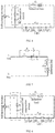
- FIG. 10 is a curve of a result of a conducted EMI test performed on a cylinder washing machine in the art.
- the conducted EMI test result shown in FIG. 10 shows that the conducted EMI of the cylinder washing machine exceeds the national standard limit.
- FIG. 11 is a curve of a result of a conducted EMI test performed on a cylinder washing machine according to an embodiment of the present disclosure.
- the conducted EMI of the cylinder washing machine is significantly improved, indicating that the system for suppressing conducted EMI provided by the embodiments of the present disclosure may effectively suppress the conducted EMI generated by the bidirectional thyristor being turned off.
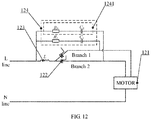
- FIG. 12 is a schematic structural diagram of a system applied to a switch element for suppressing conducted EMI applied in a cylinder washing machine according to an embodiment of the present disclosure.
- the system applied to the bidirectional thyristor for suppressing the conducted EMI as shown in FIG. 12 may be configured in the cylinder washing machine, and the results of the conducted EMI test shown in FIG. 11 may be obtained.
- the system applied to the bidirectional thyristor for suppressing the conducted EMI may include a conducted EMI suppression circuit, a motor 121 of the cylinder washing machine, and two bidirectional thyristors 122.
- the conducted EMI suppression circuit may include one inductor 123 and an RC circuit 124.
- the inductor 123 may be connected in series with the two bidirectional thyristors respectively.
- the two bidirectional thyristors 122 may be respectively connected to the motor 121.
- One of the two bidirectional thyristors 122 may be configured to control the motor 121 to rotate forwardly, and the other one of the two bidirectional thyristors 122 may be configured to control the motor 121 to rotate reversely.
- the RC circuit 124 may include two RC sub-circuits 1241. Each of the two RC sub-circuits 1241 may correspond to each of the two bidirectional thyristors 122.
- each RC sub-circuit 1241 may include one resistor and one capacitor, and the resistor and the capacitor included each RC sub-circuit 1241 may be connected in series.
Landscapes
- Engineering & Computer Science (AREA)
- Power Engineering (AREA)
- Physics & Mathematics (AREA)
- Electromagnetism (AREA)
- Electronic Switches (AREA)
- Power Conversion In General (AREA)
Abstract
Description
- The present application claims the priority of
Chinese Patent Application No. 201811580320.3 - The present disclosure relates to the field of domestic appliances, and in particular to a system applied to a switch element for conducted EMI suppression, and a domestic appliance.
- Electromagnetic Interference (EMI) refers to interference, which is caused by unwanted signals or noise and interferes reception or transmission of useful electromagnetic signals. The EMI generated by an electronic/electrical device is transmitted through wires or public power lines. The EMI transmitted in wires or public power lines may be called conducted EMI. The conducted EMI generated by the electronic/electrical device may be measured through an artificial line impedance stabilization network (LISN). Currently, any electronic/electrical device needs to pass a relevant conducted EMI test before being released into the market.
- For an electronic/electrical device that is configured with a switch element, such as a bidirectional thyristor, a metal oxide semiconductor (MOS) field effect transistor, and an insulated gate bipolar transistor (IGBT), when the electronic/electrical device connected to the above-mentioned switch element is an inductive load, and when the above-mentioned switch element is turned off, a large reverse impulse voltage may be generated at two ends of the switch element, generating the conducted EMI. For example, when a bidirectional thyristor is connected to the inductive load, and when a reverse voltage is applied to the bidirectional thyristor, a carrier accumulation effect is generated. That is, a large number of minority carriers are stored on two sides of a PN junction, resulting in a reverse blocking ability unable to be restored. The minority carriers may be drawn out of the PN junction by the reverse voltage. In this way, a larger reverse recovery current may flow through the bidirectional thyristor, and the stored minority carriers are reduced rapidly by the reverse voltage, such that a reverse recovery current attenuates rapidly, generating a larger instantaneous current change. The larger reverse impulse voltage may be generated at two ends of the bidirectional thyristor due to the inductive load and a parasitic inductance, thereby generating the conducted EMI.
- In order to enable electronic/electrical device to pass the conducted EMI test, an absorption circuit may be arranged at each of the two ends of the above-mentioned switch element to provide a bypass for the reverse recovery current.
FIG. 1 is a schematic diagram of an absorption circuit in the related art. As shown inFig. 1 , in the related art, an RC absorption circuit may be arranged, serving as the above-mentioned absorption circuit, and may be connected in parallel to the two ends of the switch element. Practically, when a frequency of conducted EMI is low, a capacitive impedance of the RC absorption circuit is high, resulting in a low insertion loss of the RC absorption circuit. When the frequency of conducted EMI is high, a stray inductance may be present to reduce the impedance of the inductive load, resulting in the insertion loss of the RC absorption circuit remaining at a low level. A filter plate may be required to be configured at a power port to pass the conducted EMI test, which increases the cost of passing the conducted EMI test. - Therefore, a significant issue to be solved in the art may refer to providing a system applied to the switch element for suppressing the conducted EMI, improving the effect of suppressing conducted EMI caused by the switch element, avoiding the configuration of the filter plate, and reducing the cost of passing the conducted EMI test.
- In view of the shortcomings in the related art, the embodiments of the present disclosure provide a system applied to the switch element for suppressing the conducted EMI, and a domestic appliance.
- According to an aspect of the present disclosure, a system applied to a switch element for suppressing conducted EMI is provided and includes a conducted EMI suppression circuit, an inductive load and at least one switch element.
- The conducted EMI suppression circuit includes one inductor and an RC circuit. The inductor is connected in series with each of the at least one switch element. The inductive load is connected with each of the at least one switch element. The inductor is connected in series with each of the at least one switch element, and is subsequently connected in parallel with the RC circuit. The conducted EMI suppression circuit is configured to suppress the conducted EMI generated by each of the at least one switch element being turned off.
- In some embodiments, the number of the at least one switch element is one, the RC circuit includes one resistor and one capacitor, and the resistor and the capacitor are connected in series.
- In some embodiments, the number of the at least one switch element is more than one. Each of the more than one switch elements is connected with the inductive load, forming more than one connecting lines. The more than one connecting lines are connected with each other in parallel. The RC circuit includes more than one RC sub-circuits. Each of the more than one RC sub-circuits corresponds to each of the more than one switch elements. The inductor is connected in series with each of the more than one switch elements, and is subsequently connected in parallel with the more than one RC sub-circuits corresponding to the connected switch elements. Each of the more than one RC sub-circuits includes one resistor and one capacitor, and the resistor and the capacitor are connected in series.
- In some embodiments, a resistance value of the resistor in each of the more than one RC sub-circuits is equal, and a capacitance value of the capacitor in each of the more than one RC sub-circuits is equal.
- In some embodiments, the number of the at least one switch element is more than one. Each of the more than one switch elements is connected with the inductive load, forming more than one connecting lines. The more than one connecting lines are connected with each other in parallel. The RC circuit includes one resistor and more than one capacitors. Each of the more than one capacitors corresponds to each of the more than one switch elements. The inductor is connected in series with each of the at least one switch element. Each of the switch elements is connected in series with the inductor, and is subsequently connected in parallel with a series circuit, and the series circuit is formed by the capacitor and the resistor corresponding to the connected switch element.
- In some embodiments, a capacitance value of each of the more than one capacitors in the RC circuit is equal.
- In some embodiments, an end of the inductor is connected to a live wire, and the other end of the inductor is connected to an end of each of the at least one switch element.
- In some embodiments, the switch element is a bidirectional thyristor, a metal oxide semiconductor field effect transistor, or an insulated gate bipolar transistor.
- In some embodiments, the inductive load is a motor.
- According to another aspect of the present disclosure, a domestic appliance is provided and includes the system applied to the switch element for suppressing conducted EMI as described in any one of the above embodiments.
- The system applied to the switch element for suppressing the conducted EMI and the domestic appliance provided by embodiments of the present disclosure may include: a conducted EMI suppression circuit, an inductive load and at least one switch element. The conducted EMI suppression circuit may include one inductor and an RC circuit. The inductor may be connected to each switch element in series, and further connected in parallel with the RC circuit. As the conducted EMI suppression circuit includes both the inductor and the RC circuit, while performing the EMI test, voltage applied to the LISN is divided, and the filter plate may be omitted, reducing the cost of passing the conducted EMI test.
- In order to illustrate technical solutions of embodiments of the present disclosure clearly, accompanying drawings for describing the embodiments will be introduced in brief. Obviously, the drawings in the following description are only some embodiments of the present application. For those skilled in the art, other drawings can be acquired based on the provided drawings without any creative work.
-
FIG. 1 is a schematic diagram of an absorption circuit in the related art. -
FIG. 2 is a schematic structural diagram of a system applied to a switch element for suppressing the conducted EMI according to an embodiment of the present disclosure. -
FIG. 3 is a diagram showing a working principle of two ends of a switch element connected to an RC absorption circuit in parallel according to an embodiment of the present disclosure. -
FIG. 4 is a circuit diagram for measuring the conducted EMI by configuring two ends of a bidirectional thyristor to connect to an RC absorption circuit in parallel according to an embodiment of the present disclosure. -
FIG. 5 is a circuit diagram showing a working principle of a system applied to a switch element for suppressing conducted EMI for a switch element according to an embodiment of the present disclosure. -
FIG. 6 is a circuit diagram for measuring a differential mode conducted EMI of a system applied to a switch element for suppressing conducted EMI according to an embodiment of the present disclosure. -
FIG. 7 is a schematic structural diagram of a system applied to a switch element for suppressing the conducted EMI according to another embodiment of the present disclosure. -
FIG. 8 is a schematic structural diagram of a system applied to a switch element for suppressing the conducted EMI according to still another embodiment of the present disclosure. -
FIG. 9 is a domestic appliance according to an embodiment of the present disclosure. -
FIG. 10 is a curve of a result of a conducted EMI test performed on a cylinder washing machine in the art according to an embodiment of the present disclosure. -
FIG. 11 is a curve of a result of a conducted EMI test performed on a cylinder washing machine according to an embodiment of the present disclosure. -
FIG. 12 is a schematic structural diagram of a system applied to a switch element for suppressing conducted EMI applied in a cylinder washing machine according to an embodiment of the present disclosure. - Reference numerals in the accompanying drawings are: 1-inductive load; 2-switch element; 3-inductor; 4-RC circuit; 10- a system applied to a switch element for suppressing conducted EMI; 71-inductive load; 72-switch element; 73-inductor; 74-RC circuit; 741-RC sub-circuit; 81-inductive load; 82-switch element; 83-inductor; 84-RC circuit; 841-resistor; 842-capacitor; 121-motor; 122- bidirectional thyristor; 123-inductor; 124-RC circuit; 1241-RC sub-circuit.
- In order to clearly illustrate objectives, technical solutions and advantages of the present disclosure, the technical solutions of the embodiments of the present disclosure will be clearly described by referring to the accompanying drawings. Obviously, the described embodiments are only some of, but not all of, the embodiments of the present disclosure. All other embodiments obtained by those of ordinary skill in the art, based on the embodiments of the present disclosure and without creative work, should fall within the scope of the present disclosure.
-
FIG. 2 is a schematic structural diagram of a system applied to a switch element for suppressing the conducted EMI according to an embodiment of the present disclosure. As shown inFIG. 2 , according to the embodiments of the present disclosure, the system applied to the switch element for suppressing conducted EMI may include a conducted EMI suppression circuit, aninductive load 1 and at least oneswitch element 2. - The conducted EMI suppression circuit may include an
inductor 3 and an RC circuit 4. Theinductor 3 is connected in series with eachswitch element 2, theinductive load 1 is connected with eachswitch element 2. Theinductor 3 is connected in series with eachswitch element 2, and is subsequently connected with the RC circuit 4 in parallel. The conducted EMI suppression circuit is configured to suppress the conducted EMI generated by eachswitch element 2 being turned off. - In detail, the
inductive load 1 may be a motor, and theswitch element 2 may be a bidirectional thyristor MOS element or an IGBT. When a plurality ofswitch elements 2 are configured, only one of the plurality ofswitch elements 2 may be in a conductive state at a time. An end of theinductor 3 may be connected to a live wire, and the other end of theinductor 3 may be connected to theswitch element 2. The RC circuit 4 may include a resistor and a capacitor, and the resistor and the capacitor are connected in series. - When the
switch element 2 is turned off, a relatively large reverse impulse voltage may be generated at two ends of theswitch element 2, generating the conducted EMI. When measuring the conducted EMI of theinductive load 1, an LISN needs to be connected between a power grid and theinductive load 1. A level of the conducted EMI may be reflected by a voltage received by a 50Ω resistor in the LISN. A source of interference may be the reverse impulse voltage generated by the switch element being turned off. A sensitive device may be the 50Ω resistor in the LISN between mains electricity and the inductive load. In order to illustrate an effect of the system applied to the switch element for suppressing the conducted EMI provided by the embodiments of the present disclosure in suppressing conducted EMI, configuring theswitch element 2 as the bidirectional thyristor may be taken as an example to compare an insertion loss of the absorption circuit shown inFIG. 1 with that of the conducted EMI suppression circuit of the system applied to the switch element for suppressing the conducted EMI provided by the embodiments of the present disclosure. -
FIG. 3 is a diagram showing a working principle of each of two ends of a switch element connected to an RC absorption circuit in parallel according to an embodiment of the present disclosure. Corresponding to the circuit structure shown inFIG. 1 , the switch element shown inFIG. 1 may be the bidirectional thyristor. As shown inFIG. 3 , in order to obtain the reverse impulse voltage of the bidirectional thyristor, the inductive load may be represented by the inductor and the resistor connected in series. An impedance may be set as ZM, the reverse impulse voltage of the bidirectional thyristor may be set as UR, and a reverse recovery current may be set as IR. According to correlation between the voltage and the current, the UR in the frequency domain may be obtained based on the following equation.
- In the equation,

- According to the substitution theorem: in a circuit having a unique solution, any two-terminal element or network, regardless of linearity of the element or the network, can be replaced by a voltage source. A function expression and a reference direction of a voltage of the voltage source may be the same as a terminal voltage of the original two-terminal element or network. Therefore, a conducted EMI measurement circuit diagram after the bidirectional thyristor being in parallel connected with the RC absorption circuit may be obtained.
- As a method for analyzing the common mode conducted EMI may be the same as a method for analyzing the differential mode conducted EMI, the differential mode conducted EMI may be analyzed in the following section.
-
FIG. 4 is a circuit diagram for measuring the conducted EMI by configuring two ends of a bidirectional thyristor to connect to an RC absorption circuit in parallel according to an embodiment of the present disclosure. In the circuit shown inFIG. 4 , when the bidirectional thyristor is not in parallel connected with the RC absorption circuit, the voltage received by the 50Ω resistor in the LISN V1 may be obtained based on the following equation.
- In the equation, the ZM may be the impedance of the inductive load, and the ZLISN may be the impedance of LISN.
- In the circuit shown in
FIG. 4 , the voltage V2 received by the 50Ω resistor in the LISN may be obtained based on the following equation.
- As a large number of minority carriers accumulated in the PN junction are drawn away by the reverse voltage, the reverse recovery current may attenuate rapidly. Therefore, the RC absorption circuit of the bidirectional thyristor does not affect the attenuation of the reverse recovery current. That is, the reverse recovery current IR in the frequency domain remains unchanged. Therefore, the insertion loss LRC of the RC absorption circuit may be obtained based on the following equation.

- According to the equation (4), when the frequency ω is low, the impedance of the capacitor may be high, resulting in a low insertion loss LRC. When the frequency co is high, the stray inductance may cause the impedance ZM of the inductive load to be reduced, such that the insertion loss LRC may not be high either.
-
FIG. 5 is a circuit diagram showing a working principle of a system applied to a switch element for suppressing conducted EMI for a switch element according to an embodiment of the present disclosure. Corresponding to the circuit structure shown inFIG. 2 , as shown inFIG. 5 , in order to obtain the reverse impulse voltage of the bidirectional thyristor, the inductive load may be represented by the inductor and the resistor being connected in series. The impedance may be set as ZM, the reverse impulse voltage of the bidirectional thyristor may be set as UR, and the reverse recovery current may be set as IR. According to correlation between the voltage and the current, the UR in the frequency domain may be obtained based on the following equation.
- In the equation,

-
FIG. 6 is a circuit diagram for measuring a differential mode conducted EMI of a system applied to a switch element for suppressing conducted EMI according to an embodiment of the present disclosure. In the circuit shown inFIG. 6 , the voltage V3 received by the 50Ω resistor in the LISN may be obtained based on the following equation.
- In the equation, // may indicate parallel connection.
- The insertion loss LRLC of the conducted EMI suppression circuit may be obtained based on the following equation.

- In order to compare the insertion loss LRLC of the conducted EMI suppression circuit and the insertion loss LRC of the RC protection circuit, the impedance ZM of the inductive load in
FIG. 4 may be set to be equal to that of the inductive load inFIG. 6 . The resistance value of the resistor in the RC protection circuit inFIG. 4 may be set to be equal to that in the conducted EMI suppression circuit inFIG. 6 . The capacitance value of the capacitor in the RC protection circuit inFIG. 4 may be set to be equal to that in the conducted EMI suppression circuit inFIG. 6 . It should be understandable that the LISN inFIG. 4 is the same as the LISN inFIG. 6 . - The following equation may be obtained by subtracting the equation (4) from the equation (7).

- According to the equation (8), the ΔL increases as the L increases. Therefore, the system for suppressing conducted EMI provided by the embodiments of the present disclosure shows a significant suppression effect on the conducted EMI.
- According to the embodiments of the present disclosure, the system applied to the switch element for suppressing conducted EMI may include the conducted EMI suppression circuit, the inductive load, and at least one switch element. The conducted EMI suppression circuit may include the inductor and the RC circuit. The inductor may be connected in series with each switch element. The inductive load may be connected to each switch element. The inductor may be connected in series with each switch element, and subsequently connected in parallel with the RC circuit. The conducted EMI suppression circuit may be configured to suppress the conducted EMI generated by the switch element being turned off. As the conducted EMI suppression circuit includes the inductor and the RC circuit, while performing the conducted EMI test, the voltage for the LISN may be divided, the filter plate may not be required, and the cost of passing the conducted EMI test may be reduced. In addition, the conducted EMI suppression circuit may further reduce reverse impulse voltage, improving the service life of the switch element.
- As shown in
FIG. 2 , based on the foregoing embodiments, further, oneswitch element 2 may be configured, and the RC circuit 4 may include one resistor and one capacitor. The resistor and the capacitor may be connected in series. -
FIG. 7 is a schematic structural diagram of a system applied to a switch element for suppressing the conducted EMI according to another embodiment of the present disclosure. A plurality ofswitch elements 72 may be configured. Connecting lines between theinductive load 71 and eachswitch element 72 may be connected in parallel with each other. Each connecting line between theswitch element 72 and theinductive load 71 may be a branch line. TheRC circuit 74 may include a plurality of RC sub-circuits 741. Each RC sub-circuit 741 corresponds to eachswitch element 72. Theinductor 73 and theswitch element 72 are connected in series, the series circuit of theinductor 73 and theswitch element 72 may subsequently be connected with the RC sub-circuit 741 corresponding to theswitch element 72 in parallel. Each RC sub-circuit 741 may include one resistor and one capacitor. The resistor and the capacitor included in each RC sub-circuit 741 may be connected in series. - Based on the foregoing embodiments, the resistance value of the resistor of each RC sub-circuit 741 may be equal, and the capacitance value of the capacitor in each RC sub-circuit 741 may be equal.
-
FIG. 8 is a schematic structural diagram of a system applied to a switch element for suppressing the conducted EMI according to still another embodiment of the present disclosure. As shown inFIG. 8 , a plurality ofswitch elements 82 may be configured. Connecting lines between theinductive load 81 and eachswitch element 82 may be connected in parallel with each other. Each connecting line between theswitch element 82 and theinductive load 81 may be a branch line. TheRC circuit 84 may include one resistor 841 and a plurality ofcapacitors 842. The resistor 841 may be connected in series with eachcapacitor 842, and each capacitor 751 may correspond to theswitch element 82. After theswitch element 82 is connected in series with theinductor 83, the series circuit of theswitch element 82 and theinductor 83 may be in parallel connected with a series circuit formed bycapacitor 842 and the resistor 841 corresponding to theswitch element 82. Compared with theRC circuit 74 shown inFIG. 7 , eachcapacitor 842 of theRC circuit 84 provided by the present embodiment may be connected to one common resistor 841. In this way, the cost of the system applied to the switch element for suppressing conducted EMI may be saved. - Based on the foregoing embodiments, further, the capacitance values of the
capacitors 842 included in theRC circuit 84 may be equal. - Based on the foregoing embodiments, further, an end of the
inductor 3 may be connected to the live wire, i.e., the L line, and the other end of theinductor 3 may be connected to an end of eachswitch element 2. - Based on the foregoing embodiments, further, the
switch element 2 may be the bidirectional thyristor, the MOS element or the IGBT. The bidirectional thyristor may be equivalent to integration of a pair of common thyristors connected in anti-parallel, which may generally be configured in AC circuits. The thyristor, also known as a silicon controlled rectifier, is a semi-controlled device that may be turned on by a control signal but may not be controlled to be turned off. The thyristor may be turned off in response to a forward current being reduced below a certain value close to zero. - Based on the foregoing embodiments, further, the
inductive load 1 may be a motor. -
FIG. 9 is a domestic appliance according to an embodiment of the present disclosure. As shown inFIG. 9 , the domestic appliance provided by the embodiment of the present disclosure may include thesystem 10 applied to the switch element for suppressing conducted EMI as described in any of the above embodiments. The domestic appliance may be, for example, an air conditioner, a washing machine, a refrigerator, and the like. - In a cylinder washing machine, two bidirectional thyristors may be configured to control a motor of the cylinder washing machine to rotate forwardly and reversely, respectively.
FIG. 10 is a curve of a result of a conducted EMI test performed on a cylinder washing machine in the art. The conducted EMI test result shown inFIG. 10 shows that the conducted EMI of the cylinder washing machine exceeds the national standard limit.FIG. 11 is a curve of a result of a conducted EMI test performed on a cylinder washing machine according to an embodiment of the present disclosure. By comparingFIG. 10 and FIG. 11 , when configuring the system applied to the switch element for suppressing the conducted EMI as provided by the embodiment of the disclosure, the conducted EMI of the cylinder washing machine is significantly improved, indicating that the system for suppressing conducted EMI provided by the embodiments of the present disclosure may effectively suppress the conducted EMI generated by the bidirectional thyristor being turned off. -
FIG. 12 is a schematic structural diagram of a system applied to a switch element for suppressing conducted EMI applied in a cylinder washing machine according to an embodiment of the present disclosure. As shown inFIG. 12 , the system applied to the bidirectional thyristor for suppressing the conducted EMI as shown inFIG. 12 may be configured in the cylinder washing machine, and the results of the conducted EMI test shown inFIG. 11 may be obtained. The system applied to the bidirectional thyristor for suppressing the conducted EMI may include a conducted EMI suppression circuit, amotor 121 of the cylinder washing machine, and twobidirectional thyristors 122. The conducted EMI suppression circuit may include oneinductor 123 and anRC circuit 124. Theinductor 123 may be connected in series with the two bidirectional thyristors respectively. The twobidirectional thyristors 122 may be respectively connected to themotor 121. One of the twobidirectional thyristors 122 may be configured to control themotor 121 to rotate forwardly, and the other one of the twobidirectional thyristors 122 may be configured to control themotor 121 to rotate reversely. TheRC circuit 124 may include twoRC sub-circuits 1241. Each of the twoRC sub-circuits 1241 may correspond to each of the twobidirectional thyristors 122. After theinductor 123 is connected in series with the twobidirectional thyristors 122, theinductor 123 may subsequently be connected in parallel to the RC sub-circuit 1241 corresponding to thebidirectional thyristor 122. Each RC sub-circuit 1241 may include one resistor and one capacitor, and the resistor and the capacitor included each RC sub-circuit 1241 may be connected in series. - At last, the above embodiments only illustrate technical solutions of the present disclosure, but do not limit the present disclosure. Although the present disclosure is described in detail by referring to the foregoing embodiments, those of ordinary skill in the art should understand that the technical solutions as described the foregoing embodiments may be modified, or some technical features may be equivalently replaced. The modification or the replacement do not cause the essence of the technical solutions to depart from the spirit and the scope of the embodiments of the present disclosure.
Claims (10)
- A system applied to a switch element for suppressing conducted EMI, comprising a conducted EMI suppression circuit, an inductive load and at least one switch element, whereinthe conducted EMI suppression circuit comprises one inductor and an RC circuit;the inductor is connected in series with each of the at least one switch element;the inductive load is connected with each of the at least one switch element;the inductor is connected in series with each of the at least one switch element, and is subsequently connected in parallel with the RC circuit; andthe conducted EMI suppression circuit is configured to suppress the conducted EMI generated by each of the at least one switch element being turned off.
- The system according to claim 1, wherein the number of the at least one switch element is one, the RC circuit comprises one resistor and one capacitor, and the resistor and the capacitor are connected in series.
- The system according to claim 1, whereinthe number of the at least one switch element is more than one;each of the switch elements is connected with the inductive load, forming connecting lines, and the connecting lines are connected with each other in parallel; the RC circuit comprises more than one RC sub-circuits;each of the RC sub-circuits corresponds to each of the switch elements;the inductor is connected in series with each of the switch elements, and is subsequently connected in parallel with the RC sub-circuits corresponding to the connected switch elements;each of the RC sub-circuits comprises one resistor and one capacitor, and the resistor and the capacitor are connected in series.
- The system according to claim 3, wherein a resistance value of the resistor in each of the RC sub-circuits is equal, and a capacitance value of the capacitor in each of the RC sub-circuits is equal.
- The system according to claim 1, whereinthe number of the at least one switch element is more than one;each of the switch elements is connected with the inductive load, forming connecting lines, and the connecting lines are connected with each other in parallel;the RC circuit comprises one resistor and more than one capacitors;each of the capacitors corresponds to each of the switch elements;each of the switch elements is connected in series with the inductor, and is subsequently connected in parallel with a series circuit, and the series circuit is formed by the capacitor and the resistor corresponding to the connected switch element.
- The system according to claim 5, wherein a capacitance value of each of the capacitors in the RC circuit is equal.
- The system according to claim 1, wherein an end of the inductor is connected to a live wire, and the other end of the inductor is connected to an end of each switch element.
- The system according to any one of claims 1 to 7, wherein the switch element is a bidirectional thyristor, a metal oxide semiconductor field effect transistor, or an insulated gate bipolar transistor.
- The system according to any one of claims 1 to 7, wherein the inductive load is a motor.
- A domestic appliance, comprising the system applied to the switch element for suppressing conducted EMI according to any one claims 1 to 9.
Applications Claiming Priority (2)
| Application Number | Priority Date | Filing Date | Title |
|---|---|---|---|
| CN201811580320.3A CN111355366B (en) | 2018-12-24 | 2018-12-24 | System for inhibiting conduction EMI (electro-magnetic interference) for switch tube and household appliance |
| PCT/CN2019/122875 WO2020134915A1 (en) | 2018-12-24 | 2019-12-04 | Conductive emi suppression system for switch tube, and household appliance |
Publications (3)
| Publication Number | Publication Date |
|---|---|
| EP3863167A1 true EP3863167A1 (en) | 2021-08-11 |
| EP3863167A4 EP3863167A4 (en) | 2021-11-17 |
| EP3863167B1 EP3863167B1 (en) | 2023-10-11 |
Family
ID=71126468
Family Applications (1)
| Application Number | Title | Priority Date | Filing Date |
|---|---|---|---|
| EP19904494.2A Active EP3863167B1 (en) | 2018-12-24 | 2019-12-04 | Conductive emi suppression system for switch tube, and household appliance |
Country Status (4)
| Country | Link |
|---|---|
| US (1) | US12063025B2 (en) |
| EP (1) | EP3863167B1 (en) |
| CN (2) | CN111355366B (en) |
| WO (1) | WO2020134915A1 (en) |
Families Citing this family (2)
| Publication number | Priority date | Publication date | Assignee | Title |
|---|---|---|---|---|
| EP3654477A1 (en) * | 2018-11-15 | 2020-05-20 | Siemens Aktiengesellschaft | Electronic switch with surge protector |
| CN113848404B (en) * | 2021-09-13 | 2024-09-13 | 广州汽车集团股份有限公司 | Test circuit and test method for influence of inductive load on EMC performance of whole vehicle |
Family Cites Families (16)
| Publication number | Priority date | Publication date | Assignee | Title |
|---|---|---|---|---|
| SE395573B (en) | 1975-11-19 | 1977-08-15 | Asea Ab | HIGH VOLTAGE TYRISTOR VALVE WITH OVERVOLTAGE PROTECTION |
| DE2640623C2 (en) | 1976-09-09 | 1983-04-07 | Siemens AG, 1000 Berlin und 8000 München | Protective circuit for several thyristors connected in parallel |
| US4422030A (en) * | 1980-08-15 | 1983-12-20 | Mcallise Raymond J | A.C. Motor control |
| JPS57101007U (en) * | 1980-12-15 | 1982-06-22 | ||
| US4594650A (en) * | 1983-04-19 | 1986-06-10 | Mitsubishi Denki Kabushiki Kaisha | Inverter device |
| DE3500786A1 (en) | 1985-01-11 | 1986-07-17 | Siemens AG, 1000 Berlin und 8000 München | STATIC BLIND COMPENSATOR |
| JP3798095B2 (en) * | 1996-01-31 | 2006-07-19 | 東北リコー株式会社 | Switching power supply |
| US6215266B1 (en) * | 1997-09-02 | 2001-04-10 | Seagate Technology Llc | System and method for low acoustic noise spindle motor commutation |
| US5990654A (en) | 1998-01-21 | 1999-11-23 | Allen-Bradley Company, Llc | Apparatus for eliminating motor voltage reflections and reducing EMI currents |
| GB2503890A (en) * | 2012-07-10 | 2014-01-15 | Nujira Ltd | Switched mode power supply having interference suppression capacitors |
| CN104538963B (en) | 2014-11-13 | 2017-04-19 | 美国环境电力公司 | Adaptive filter |
| CN204394243U (en) * | 2014-12-25 | 2015-06-17 | 九阳股份有限公司 | A kind of soy bean milk making machine |
| CN206099746U (en) | 2016-10-28 | 2017-04-12 | 佛山市顺德区美的电热电器制造有限公司 | Low pass filter circuit, DC power supply and domestic appliance |
| US9837952B1 (en) * | 2016-12-16 | 2017-12-05 | Hamilton Sundstrand Corporation | Reducing resonant effects of reactive loads in electric motor systems |
| CN107026571A (en) * | 2016-12-26 | 2017-08-08 | 国网江西省电力公司电力科学研究院 | A switching power supply device |
| CN111740586A (en) * | 2020-08-14 | 2020-10-02 | 嘉兴行适安车联网信息科技有限公司 | A kind of RC absorption circuit to improve EMC performance |
-
2018
- 2018-12-24 CN CN201811580320.3A patent/CN111355366B/en active Active
- 2018-12-24 CN CN202110750474.8A patent/CN113364271A/en active Pending
-
2019
- 2019-12-04 EP EP19904494.2A patent/EP3863167B1/en active Active
- 2019-12-04 WO PCT/CN2019/122875 patent/WO2020134915A1/en not_active Ceased
- 2019-12-04 US US17/295,041 patent/US12063025B2/en active Active
Also Published As
| Publication number | Publication date |
|---|---|
| CN113364271A (en) | 2021-09-07 |
| US12063025B2 (en) | 2024-08-13 |
| EP3863167B1 (en) | 2023-10-11 |
| CN111355366B (en) | 2021-12-28 |
| US20220014164A1 (en) | 2022-01-13 |
| CN111355366A (en) | 2020-06-30 |
| EP3863167A4 (en) | 2021-11-17 |
| WO2020134915A1 (en) | 2020-07-02 |
Similar Documents
| Publication | Publication Date | Title |
|---|---|---|
| CN105591366B (en) | Frequency converter and the method for identifying and blocking fault current in frequency converter | |
| CN104377667B (en) | High-voltage direct-current line pilot protection method based on boundary energy | |
| Antoniali et al. | Measurement and characterization of load impedances in home power line grids | |
| CN201328145Y (en) | Transient interference suppressor | |
| US9396866B2 (en) | Blocker of geomagnetically induced currents (GIC) | |
| CN106468752B (en) | Integrated Fault Location RCD Snubber Circuit and Fault Location Method for Solid State Circuit Breaker | |
| CN115275951A (en) | Method and system for protecting single-end capacity of borderless flexible direct-current power distribution network | |
| CN104614642B (en) | A kind of small current earthing wire-selecting method | |
| EP3863167A1 (en) | Conductive emi suppression system for switch tube, and household appliance | |
| CN209446685U (en) | A kind of system for eliminating electrical fast transient (eft) interference | |
| CN106328361A (en) | Resonation elimination mechanism used in arc-resonation elimination device | |
| CN109412404A (en) | A kind of electric appliance EMC circuit and household electrical appliance | |
| CN110161292A (en) | A kind of distribution line ground fault voltage signal acquisition device | |
| CN206773162U (en) | Frequency converter status monitoring circuit and the frequency converter comprising the circuit | |
| CN111351995B (en) | System for restraining conducted EMI and household appliance | |
| CN219287146U (en) | Dynamometer resonance suppression device and dynamometer system based on C-type filter | |
| CN111404129B (en) | A protection method based on the operating characteristics of DC circuit breakers in a flexible DC transmission system | |
| CN208971139U (en) | A kind of signal isolating device of anti-electric railway traction reflux interference | |
| CN103472353B (en) | A kind of method of searching direct current swinging cross | |
| Alaya et al. | Coupling unit for narrowband power line communications channel measurement | |
| KR102870872B1 (en) | EMP Power-line Filter | |
| CN207460168U (en) | A kind of carrier signal measuring device | |
| Swamy et al. | A new normal mode dv/dt filter with resistor failure detection circuit | |
| CN205565718U (en) | Lightning -proof grounding device | |
| CN221078780U (en) | Effective value detection circuit and device of alternating voltage and household appliance |
Legal Events
| Date | Code | Title | Description |
|---|---|---|---|
| STAA | Information on the status of an ep patent application or granted ep patent |
Free format text: STATUS: THE INTERNATIONAL PUBLICATION HAS BEEN MADE |
|
| PUAI | Public reference made under article 153(3) epc to a published international application that has entered the european phase |
Free format text: ORIGINAL CODE: 0009012 |
|
| STAA | Information on the status of an ep patent application or granted ep patent |
Free format text: STATUS: REQUEST FOR EXAMINATION WAS MADE |
|
| 17P | Request for examination filed |
Effective date: 20210504 |
|
| AK | Designated contracting states |
Kind code of ref document: A1 Designated state(s): AL AT BE BG CH CY CZ DE DK EE ES FI FR GB GR HR HU IE IS IT LI LT LU LV MC MK MT NL NO PL PT RO RS SE SI SK SM TR |
|
| A4 | Supplementary search report drawn up and despatched |
Effective date: 20211018 |
|
| RIC1 | Information provided on ipc code assigned before grant |
Ipc: H02M 1/34 20070101ALI20211012BHEP Ipc: H02M 5/22 20060101ALI20211012BHEP Ipc: H02M 1/44 20070101AFI20211012BHEP |
|
| DAV | Request for validation of the european patent (deleted) | ||
| DAX | Request for extension of the european patent (deleted) | ||
| STAA | Information on the status of an ep patent application or granted ep patent |
Free format text: STATUS: EXAMINATION IS IN PROGRESS |
|
| 17Q | First examination report despatched |
Effective date: 20220610 |
|
| GRAP | Despatch of communication of intention to grant a patent |
Free format text: ORIGINAL CODE: EPIDOSNIGR1 |
|
| STAA | Information on the status of an ep patent application or granted ep patent |
Free format text: STATUS: GRANT OF PATENT IS INTENDED |
|
| INTG | Intention to grant announced |
Effective date: 20230707 |
|
| GRAS | Grant fee paid |
Free format text: ORIGINAL CODE: EPIDOSNIGR3 |
|
| GRAA | (expected) grant |
Free format text: ORIGINAL CODE: 0009210 |
|
| STAA | Information on the status of an ep patent application or granted ep patent |
Free format text: STATUS: THE PATENT HAS BEEN GRANTED |
|
| AK | Designated contracting states |
Kind code of ref document: B1 Designated state(s): AL AT BE BG CH CY CZ DE DK EE ES FI FR GB GR HR HU IE IS IT LI LT LU LV MC MK MT NL NO PL PT RO RS SE SI SK SM TR |
|
| REG | Reference to a national code |
Ref country code: GB Ref legal event code: FG4D |
|
| REG | Reference to a national code |
Ref country code: CH Ref legal event code: EP |
|
| REG | Reference to a national code |
Ref country code: DE Ref legal event code: R096 Ref document number: 602019039381 Country of ref document: DE |
|
| REG | Reference to a national code |
Ref country code: IE Ref legal event code: FG4D |
|
| REG | Reference to a national code |
Ref country code: LT Ref legal event code: MG9D |
|
| REG | Reference to a national code |
Ref country code: NL Ref legal event code: MP Effective date: 20231011 |
|
| REG | Reference to a national code |
Ref country code: AT Ref legal event code: MK05 Ref document number: 1621230 Country of ref document: AT Kind code of ref document: T Effective date: 20231011 |
|
| PG25 | Lapsed in a contracting state [announced via postgrant information from national office to epo] |
Ref country code: NL Free format text: LAPSE BECAUSE OF FAILURE TO SUBMIT A TRANSLATION OF THE DESCRIPTION OR TO PAY THE FEE WITHIN THE PRESCRIBED TIME-LIMIT Effective date: 20231011 |
|
| PG25 | Lapsed in a contracting state [announced via postgrant information from national office to epo] |
Ref country code: GR Free format text: LAPSE BECAUSE OF FAILURE TO SUBMIT A TRANSLATION OF THE DESCRIPTION OR TO PAY THE FEE WITHIN THE PRESCRIBED TIME-LIMIT Effective date: 20240112 |
|
| PG25 | Lapsed in a contracting state [announced via postgrant information from national office to epo] |
Ref country code: IS Free format text: LAPSE BECAUSE OF FAILURE TO SUBMIT A TRANSLATION OF THE DESCRIPTION OR TO PAY THE FEE WITHIN THE PRESCRIBED TIME-LIMIT Effective date: 20240211 |
|
| PG25 | Lapsed in a contracting state [announced via postgrant information from national office to epo] |
Ref country code: LT Free format text: LAPSE BECAUSE OF FAILURE TO SUBMIT A TRANSLATION OF THE DESCRIPTION OR TO PAY THE FEE WITHIN THE PRESCRIBED TIME-LIMIT Effective date: 20231011 |
|
| PG25 | Lapsed in a contracting state [announced via postgrant information from national office to epo] |
Ref country code: AT Free format text: LAPSE BECAUSE OF FAILURE TO SUBMIT A TRANSLATION OF THE DESCRIPTION OR TO PAY THE FEE WITHIN THE PRESCRIBED TIME-LIMIT Effective date: 20231011 |
|
| PG25 | Lapsed in a contracting state [announced via postgrant information from national office to epo] |
Ref country code: ES Free format text: LAPSE BECAUSE OF FAILURE TO SUBMIT A TRANSLATION OF THE DESCRIPTION OR TO PAY THE FEE WITHIN THE PRESCRIBED TIME-LIMIT Effective date: 20231011 |
|
| PG25 | Lapsed in a contracting state [announced via postgrant information from national office to epo] |
Ref country code: LT Free format text: LAPSE BECAUSE OF FAILURE TO SUBMIT A TRANSLATION OF THE DESCRIPTION OR TO PAY THE FEE WITHIN THE PRESCRIBED TIME-LIMIT Effective date: 20231011 Ref country code: IS Free format text: LAPSE BECAUSE OF FAILURE TO SUBMIT A TRANSLATION OF THE DESCRIPTION OR TO PAY THE FEE WITHIN THE PRESCRIBED TIME-LIMIT Effective date: 20240211 Ref country code: GR Free format text: LAPSE BECAUSE OF FAILURE TO SUBMIT A TRANSLATION OF THE DESCRIPTION OR TO PAY THE FEE WITHIN THE PRESCRIBED TIME-LIMIT Effective date: 20240112 Ref country code: ES Free format text: LAPSE BECAUSE OF FAILURE TO SUBMIT A TRANSLATION OF THE DESCRIPTION OR TO PAY THE FEE WITHIN THE PRESCRIBED TIME-LIMIT Effective date: 20231011 Ref country code: BG Free format text: LAPSE BECAUSE OF FAILURE TO SUBMIT A TRANSLATION OF THE DESCRIPTION OR TO PAY THE FEE WITHIN THE PRESCRIBED TIME-LIMIT Effective date: 20240111 Ref country code: AT Free format text: LAPSE BECAUSE OF FAILURE TO SUBMIT A TRANSLATION OF THE DESCRIPTION OR TO PAY THE FEE WITHIN THE PRESCRIBED TIME-LIMIT Effective date: 20231011 Ref country code: PT Free format text: LAPSE BECAUSE OF FAILURE TO SUBMIT A TRANSLATION OF THE DESCRIPTION OR TO PAY THE FEE WITHIN THE PRESCRIBED TIME-LIMIT Effective date: 20240212 |
|
| PG25 | Lapsed in a contracting state [announced via postgrant information from national office to epo] |
Ref country code: SE Free format text: LAPSE BECAUSE OF FAILURE TO SUBMIT A TRANSLATION OF THE DESCRIPTION OR TO PAY THE FEE WITHIN THE PRESCRIBED TIME-LIMIT Effective date: 20231011 Ref country code: RS Free format text: LAPSE BECAUSE OF FAILURE TO SUBMIT A TRANSLATION OF THE DESCRIPTION OR TO PAY THE FEE WITHIN THE PRESCRIBED TIME-LIMIT Effective date: 20231011 Ref country code: PL Free format text: LAPSE BECAUSE OF FAILURE TO SUBMIT A TRANSLATION OF THE DESCRIPTION OR TO PAY THE FEE WITHIN THE PRESCRIBED TIME-LIMIT Effective date: 20231011 Ref country code: NO Free format text: LAPSE BECAUSE OF FAILURE TO SUBMIT A TRANSLATION OF THE DESCRIPTION OR TO PAY THE FEE WITHIN THE PRESCRIBED TIME-LIMIT Effective date: 20240111 Ref country code: LV Free format text: LAPSE BECAUSE OF FAILURE TO SUBMIT A TRANSLATION OF THE DESCRIPTION OR TO PAY THE FEE WITHIN THE PRESCRIBED TIME-LIMIT Effective date: 20231011 Ref country code: HR Free format text: LAPSE BECAUSE OF FAILURE TO SUBMIT A TRANSLATION OF THE DESCRIPTION OR TO PAY THE FEE WITHIN THE PRESCRIBED TIME-LIMIT Effective date: 20231011 |
|
| P01 | Opt-out of the competence of the unified patent court (upc) registered |
Effective date: 20240520 |
|
| PG25 | Lapsed in a contracting state [announced via postgrant information from national office to epo] |
Ref country code: DK Free format text: LAPSE BECAUSE OF FAILURE TO SUBMIT A TRANSLATION OF THE DESCRIPTION OR TO PAY THE FEE WITHIN THE PRESCRIBED TIME-LIMIT Effective date: 20231011 |
|
| REG | Reference to a national code |
Ref country code: DE Ref legal event code: R097 Ref document number: 602019039381 Country of ref document: DE |
|
| PG25 | Lapsed in a contracting state [announced via postgrant information from national office to epo] |
Ref country code: CZ Free format text: LAPSE BECAUSE OF FAILURE TO SUBMIT A TRANSLATION OF THE DESCRIPTION OR TO PAY THE FEE WITHIN THE PRESCRIBED TIME-LIMIT Effective date: 20231011 |
|
| PG25 | Lapsed in a contracting state [announced via postgrant information from national office to epo] |
Ref country code: SK Free format text: LAPSE BECAUSE OF FAILURE TO SUBMIT A TRANSLATION OF THE DESCRIPTION OR TO PAY THE FEE WITHIN THE PRESCRIBED TIME-LIMIT Effective date: 20231011 |
|
| PG25 | Lapsed in a contracting state [announced via postgrant information from national office to epo] |
Ref country code: SM Free format text: LAPSE BECAUSE OF FAILURE TO SUBMIT A TRANSLATION OF THE DESCRIPTION OR TO PAY THE FEE WITHIN THE PRESCRIBED TIME-LIMIT Effective date: 20231011 Ref country code: SK Free format text: LAPSE BECAUSE OF FAILURE TO SUBMIT A TRANSLATION OF THE DESCRIPTION OR TO PAY THE FEE WITHIN THE PRESCRIBED TIME-LIMIT Effective date: 20231011 Ref country code: RO Free format text: LAPSE BECAUSE OF FAILURE TO SUBMIT A TRANSLATION OF THE DESCRIPTION OR TO PAY THE FEE WITHIN THE PRESCRIBED TIME-LIMIT Effective date: 20231011 Ref country code: IT Free format text: LAPSE BECAUSE OF FAILURE TO SUBMIT A TRANSLATION OF THE DESCRIPTION OR TO PAY THE FEE WITHIN THE PRESCRIBED TIME-LIMIT Effective date: 20231011 Ref country code: EE Free format text: LAPSE BECAUSE OF FAILURE TO SUBMIT A TRANSLATION OF THE DESCRIPTION OR TO PAY THE FEE WITHIN THE PRESCRIBED TIME-LIMIT Effective date: 20231011 Ref country code: DK Free format text: LAPSE BECAUSE OF FAILURE TO SUBMIT A TRANSLATION OF THE DESCRIPTION OR TO PAY THE FEE WITHIN THE PRESCRIBED TIME-LIMIT Effective date: 20231011 Ref country code: CZ Free format text: LAPSE BECAUSE OF FAILURE TO SUBMIT A TRANSLATION OF THE DESCRIPTION OR TO PAY THE FEE WITHIN THE PRESCRIBED TIME-LIMIT Effective date: 20231011 |
|
| REG | Reference to a national code |
Ref country code: CH Ref legal event code: PL |
|
| PLBE | No opposition filed within time limit |
Free format text: ORIGINAL CODE: 0009261 |
|
| STAA | Information on the status of an ep patent application or granted ep patent |
Free format text: STATUS: NO OPPOSITION FILED WITHIN TIME LIMIT |
|
| PG25 | Lapsed in a contracting state [announced via postgrant information from national office to epo] |
Ref country code: LU Free format text: LAPSE BECAUSE OF NON-PAYMENT OF DUE FEES Effective date: 20231204 |
|
| PG25 | Lapsed in a contracting state [announced via postgrant information from national office to epo] |
Ref country code: MC Free format text: LAPSE BECAUSE OF FAILURE TO SUBMIT A TRANSLATION OF THE DESCRIPTION OR TO PAY THE FEE WITHIN THE PRESCRIBED TIME-LIMIT Effective date: 20231011 |
|
| REG | Reference to a national code |
Ref country code: BE Ref legal event code: MM Effective date: 20231231 |
|
| PG25 | Lapsed in a contracting state [announced via postgrant information from national office to epo] |
Ref country code: MC Free format text: LAPSE BECAUSE OF FAILURE TO SUBMIT A TRANSLATION OF THE DESCRIPTION OR TO PAY THE FEE WITHIN THE PRESCRIBED TIME-LIMIT Effective date: 20231011 Ref country code: LU Free format text: LAPSE BECAUSE OF NON-PAYMENT OF DUE FEES Effective date: 20231204 |
|
| 26N | No opposition filed |
Effective date: 20240712 |
|
| REG | Reference to a national code |
Ref country code: IE Ref legal event code: MM4A |
|
| PG25 | Lapsed in a contracting state [announced via postgrant information from national office to epo] |
Ref country code: IE Free format text: LAPSE BECAUSE OF NON-PAYMENT OF DUE FEES Effective date: 20231204 |
|
| PG25 | Lapsed in a contracting state [announced via postgrant information from national office to epo] |
Ref country code: BE Free format text: LAPSE BECAUSE OF NON-PAYMENT OF DUE FEES Effective date: 20231231 |
|
| PG25 | Lapsed in a contracting state [announced via postgrant information from national office to epo] |
Ref country code: CH Free format text: LAPSE BECAUSE OF NON-PAYMENT OF DUE FEES Effective date: 20231231 |
|
| PG25 | Lapsed in a contracting state [announced via postgrant information from national office to epo] |
Ref country code: SI Free format text: LAPSE BECAUSE OF FAILURE TO SUBMIT A TRANSLATION OF THE DESCRIPTION OR TO PAY THE FEE WITHIN THE PRESCRIBED TIME-LIMIT Effective date: 20231011 |
|
| PG25 | Lapsed in a contracting state [announced via postgrant information from national office to epo] |
Ref country code: SI Free format text: LAPSE BECAUSE OF FAILURE TO SUBMIT A TRANSLATION OF THE DESCRIPTION OR TO PAY THE FEE WITHIN THE PRESCRIBED TIME-LIMIT Effective date: 20231011 Ref country code: IE Free format text: LAPSE BECAUSE OF NON-PAYMENT OF DUE FEES Effective date: 20231204 Ref country code: CH Free format text: LAPSE BECAUSE OF NON-PAYMENT OF DUE FEES Effective date: 20231231 Ref country code: BE Free format text: LAPSE BECAUSE OF NON-PAYMENT OF DUE FEES Effective date: 20231231 |
|
| PG25 | Lapsed in a contracting state [announced via postgrant information from national office to epo] |
Ref country code: FI Free format text: LAPSE BECAUSE OF FAILURE TO SUBMIT A TRANSLATION OF THE DESCRIPTION OR TO PAY THE FEE WITHIN THE PRESCRIBED TIME-LIMIT Effective date: 20231011 |
|
| PG25 | Lapsed in a contracting state [announced via postgrant information from national office to epo] |
Ref country code: CY Free format text: LAPSE BECAUSE OF FAILURE TO SUBMIT A TRANSLATION OF THE DESCRIPTION OR TO PAY THE FEE WITHIN THE PRESCRIBED TIME-LIMIT; INVALID AB INITIO Effective date: 20191204 |
|
| PG25 | Lapsed in a contracting state [announced via postgrant information from national office to epo] |
Ref country code: HU Free format text: LAPSE BECAUSE OF FAILURE TO SUBMIT A TRANSLATION OF THE DESCRIPTION OR TO PAY THE FEE WITHIN THE PRESCRIBED TIME-LIMIT; INVALID AB INITIO Effective date: 20191204 |
|
| PG25 | Lapsed in a contracting state [announced via postgrant information from national office to epo] |
Ref country code: TR Free format text: LAPSE BECAUSE OF FAILURE TO SUBMIT A TRANSLATION OF THE DESCRIPTION OR TO PAY THE FEE WITHIN THE PRESCRIBED TIME-LIMIT Effective date: 20231011 |
|
| PGFP | Annual fee paid to national office [announced via postgrant information from national office to epo] |
Ref country code: DE Payment date: 20251212 Year of fee payment: 7 |
|
| PGFP | Annual fee paid to national office [announced via postgrant information from national office to epo] |
Ref country code: GB Payment date: 20251211 Year of fee payment: 7 |
|
| PGFP | Annual fee paid to national office [announced via postgrant information from national office to epo] |
Ref country code: FR Payment date: 20251212 Year of fee payment: 7 |