EP3863053B1 - Pin mesa diodes with over-current protection - Google Patents
Pin mesa diodes with over-current protection Download PDFInfo
- Publication number
- EP3863053B1 EP3863053B1 EP21155753.3A EP21155753A EP3863053B1 EP 3863053 B1 EP3863053 B1 EP 3863053B1 EP 21155753 A EP21155753 A EP 21155753A EP 3863053 B1 EP3863053 B1 EP 3863053B1
- Authority
- EP
- European Patent Office
- Prior art keywords
- trench
- layer
- contact
- recited
- absorption layer
- Prior art date
- Legal status (The legal status is an assumption and is not a legal conclusion. Google has not performed a legal analysis and makes no representation as to the accuracy of the status listed.)
- Active
Links
Images
Classifications
-
- H—ELECTRICITY
- H10—SEMICONDUCTOR DEVICES; ELECTRIC SOLID-STATE DEVICES NOT OTHERWISE PROVIDED FOR
- H10F—INORGANIC SEMICONDUCTOR DEVICES SENSITIVE TO INFRARED RADIATION, LIGHT, ELECTROMAGNETIC RADIATION OF SHORTER WAVELENGTH OR CORPUSCULAR RADIATION
- H10F30/00—Individual radiation-sensitive semiconductor devices in which radiation controls the flow of current through the devices, e.g. photodetectors
- H10F30/20—Individual radiation-sensitive semiconductor devices in which radiation controls the flow of current through the devices, e.g. photodetectors the devices having potential barriers, e.g. phototransistors
- H10F30/21—Individual radiation-sensitive semiconductor devices in which radiation controls the flow of current through the devices, e.g. photodetectors the devices having potential barriers, e.g. phototransistors the devices being sensitive to infrared, visible or ultraviolet radiation
- H10F30/22—Individual radiation-sensitive semiconductor devices in which radiation controls the flow of current through the devices, e.g. photodetectors the devices having potential barriers, e.g. phototransistors the devices being sensitive to infrared, visible or ultraviolet radiation the devices having only one potential barrier, e.g. photodiodes
- H10F30/223—Individual radiation-sensitive semiconductor devices in which radiation controls the flow of current through the devices, e.g. photodetectors the devices having potential barriers, e.g. phototransistors the devices being sensitive to infrared, visible or ultraviolet radiation the devices having only one potential barrier, e.g. photodiodes the potential barrier being a PIN barrier
-
- H—ELECTRICITY
- H10—SEMICONDUCTOR DEVICES; ELECTRIC SOLID-STATE DEVICES NOT OTHERWISE PROVIDED FOR
- H10F—INORGANIC SEMICONDUCTOR DEVICES SENSITIVE TO INFRARED RADIATION, LIGHT, ELECTROMAGNETIC RADIATION OF SHORTER WAVELENGTH OR CORPUSCULAR RADIATION
- H10F39/00—Integrated devices, or assemblies of multiple devices, comprising at least one element covered by group H10F30/00, e.g. radiation detectors comprising photodiode arrays
- H10F39/10—Integrated devices
- H10F39/107—Integrated devices having multiple elements covered by H10F30/00 in a repetitive configuration, e.g. radiation detectors comprising photodiode arrays
-
- H—ELECTRICITY
- H10—SEMICONDUCTOR DEVICES; ELECTRIC SOLID-STATE DEVICES NOT OTHERWISE PROVIDED FOR
- H10F—INORGANIC SEMICONDUCTOR DEVICES SENSITIVE TO INFRARED RADIATION, LIGHT, ELECTROMAGNETIC RADIATION OF SHORTER WAVELENGTH OR CORPUSCULAR RADIATION
- H10F39/00—Integrated devices, or assemblies of multiple devices, comprising at least one element covered by group H10F30/00, e.g. radiation detectors comprising photodiode arrays
- H10F39/011—Manufacture or treatment of image sensors covered by group H10F39/12
-
- H—ELECTRICITY
- H10—SEMICONDUCTOR DEVICES; ELECTRIC SOLID-STATE DEVICES NOT OTHERWISE PROVIDED FOR
- H10F—INORGANIC SEMICONDUCTOR DEVICES SENSITIVE TO INFRARED RADIATION, LIGHT, ELECTROMAGNETIC RADIATION OF SHORTER WAVELENGTH OR CORPUSCULAR RADIATION
- H10F39/00—Integrated devices, or assemblies of multiple devices, comprising at least one element covered by group H10F30/00, e.g. radiation detectors comprising photodiode arrays
- H10F39/80—Constructional details of image sensors
-
- H—ELECTRICITY
- H10—SEMICONDUCTOR DEVICES; ELECTRIC SOLID-STATE DEVICES NOT OTHERWISE PROVIDED FOR
- H10F—INORGANIC SEMICONDUCTOR DEVICES SENSITIVE TO INFRARED RADIATION, LIGHT, ELECTROMAGNETIC RADIATION OF SHORTER WAVELENGTH OR CORPUSCULAR RADIATION
- H10F39/00—Integrated devices, or assemblies of multiple devices, comprising at least one element covered by group H10F30/00, e.g. radiation detectors comprising photodiode arrays
- H10F39/80—Constructional details of image sensors
- H10F39/802—Geometry or disposition of elements in pixels, e.g. address-lines or gate electrodes
- H10F39/8027—Geometry of the photosensitive area
-
- H—ELECTRICITY
- H10—SEMICONDUCTOR DEVICES; ELECTRIC SOLID-STATE DEVICES NOT OTHERWISE PROVIDED FOR
- H10F—INORGANIC SEMICONDUCTOR DEVICES SENSITIVE TO INFRARED RADIATION, LIGHT, ELECTROMAGNETIC RADIATION OF SHORTER WAVELENGTH OR CORPUSCULAR RADIATION
- H10F39/00—Integrated devices, or assemblies of multiple devices, comprising at least one element covered by group H10F30/00, e.g. radiation detectors comprising photodiode arrays
- H10F39/80—Constructional details of image sensors
- H10F39/806—Optical elements or arrangements associated with the image sensors
- H10F39/8067—Reflectors
-
- H—ELECTRICITY
- H10—SEMICONDUCTOR DEVICES; ELECTRIC SOLID-STATE DEVICES NOT OTHERWISE PROVIDED FOR
- H10F—INORGANIC SEMICONDUCTOR DEVICES SENSITIVE TO INFRARED RADIATION, LIGHT, ELECTROMAGNETIC RADIATION OF SHORTER WAVELENGTH OR CORPUSCULAR RADIATION
- H10F39/00—Integrated devices, or assemblies of multiple devices, comprising at least one element covered by group H10F30/00, e.g. radiation detectors comprising photodiode arrays
- H10F39/80—Constructional details of image sensors
- H10F39/809—Constructional details of image sensors of hybrid image sensors
-
- H—ELECTRICITY
- H10—SEMICONDUCTOR DEVICES; ELECTRIC SOLID-STATE DEVICES NOT OTHERWISE PROVIDED FOR
- H10F—INORGANIC SEMICONDUCTOR DEVICES SENSITIVE TO INFRARED RADIATION, LIGHT, ELECTROMAGNETIC RADIATION OF SHORTER WAVELENGTH OR CORPUSCULAR RADIATION
- H10F39/00—Integrated devices, or assemblies of multiple devices, comprising at least one element covered by group H10F30/00, e.g. radiation detectors comprising photodiode arrays
- H10F39/80—Constructional details of image sensors
- H10F39/811—Interconnections
-
- H—ELECTRICITY
- H10—SEMICONDUCTOR DEVICES; ELECTRIC SOLID-STATE DEVICES NOT OTHERWISE PROVIDED FOR
- H10F—INORGANIC SEMICONDUCTOR DEVICES SENSITIVE TO INFRARED RADIATION, LIGHT, ELECTROMAGNETIC RADIATION OF SHORTER WAVELENGTH OR CORPUSCULAR RADIATION
- H10F39/00—Integrated devices, or assemblies of multiple devices, comprising at least one element covered by group H10F30/00, e.g. radiation detectors comprising photodiode arrays
- H10F39/10—Integrated devices
- H10F39/12—Image sensors
- H10F39/18—Complementary metal-oxide-semiconductor [CMOS] image sensors; Photodiode array image sensors
- H10F39/184—Infrared image sensors
Definitions
- the present disclosure relates to diodes, and more particularly to photodiodes such as used in pixels for imaging.
- a photodetector array (PDA) with mesa structures improve modulation transfer function (MTF) of an imaging device.
- PDA photodetector array
- MTF modulation transfer function
- the overflow contact can surround the mesa.
- the pixel can be one of a plurality of similar pixels arranged in a grid pattern, wherein the trench separates each pixel from adjacent ones of the pixels.
- the overflow contact can be seated in a base of the trench, forming an overflow contact grid wherein the pixels are in the spaces of the overflow contact grid between intersecting lines of the overflow contact grid.
- the trench has a base between sidewalls of the trench, wherein the overflow contact is seated on the base, and wherein there is lateral clearance on the base between the overflow contact and each of the sidewalls.
- the overflow contact seats against a transparent conductive oxide (TCO) that in turn contacts the absorption layer.
- TCO transparent conductive oxide
- the TCO can include multiple layers of ZnO, TiO 2 and/or Indium Tin Oxide (ITO).
- ITO Indium Tin Oxide
- the TCO is formed in a gap within a SiNx layer.
- a contact metal can be electrically connected to the diffusion layer, configured to electrically connect the diffusion layer to a read-out integrated circuit (ROIC).
- ROIC read-out integrated circuit
- the overflow contact can be metallic.
- a cap layer can be deposited on the absorption layer opposite a substrate.
- the cap layer can include InP.
- a SiNx layer can be included over the cap layer.
- the SiNx layer can directly contact the absorption layer within the trench.
- An anti-reflective layer can be deposited on the substrate opposite the absorption layer.
- the absorption layer can include InGaAs, wherein the pixel is sensitive to illumination in infrared wavelengths. It is also contemplated that the absorption layer can include Si, wherein the pixel is sensitive to illumination in visible light wavelengths.
- the method includes depositing a SiNx layer on the absorption layer after forming the trench, wherein forming the overflow contact in the trench is performed after depositing the SiNx layer.
- Forming the overflow contact in the trench includes forming the overflow contact on a transparent oxide layer (TCO) formed in a gap in the SiNx layer.
- TCO transparent oxide layer
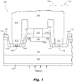
- Fig. 1 a partial view of an embodiment of a system in accordance with the disclosure is shown in Fig. 1 and is designated generally by reference character 100.
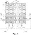
- Fig. 2 Other embodiments of systems in accordance with the disclosure, or aspects thereof, are provided in Fig. 2 , as will be described.
- the systems and methods described herein can be used to reduce excess current, increase sensitivity, and reduce stress on read-out integrated circuits (ROICs) in imaging devices.
- ROICs read-out integrated circuits
- the system 100 includes a pixel 102 including a diffusion layer 104 in contact with an absorption layer 106.
- the diffusion layer 104 and absorption layer 106 are in contact with one another along an interface 108 that is inside of a mesa 109.
- a trench 110 is defined in the absorption layer 106 surrounding the mesa 109.
- An overflow contact 112 is seated in the trench 110.
- the pixel 102 is one of a plurality of similar pixels 102 arranged in a square tiled grid pattern 114, a portion of which is indicated with reference character 114 and the associated phantom lines in Fig. 2 .
- the trench 110 separates each pixel 102 from adjacent ones of the pixels 102.
- the overflow contact 112 surrounds each mesa 109.
- the overflow contact 112 is seated in a base 116 of the trench 110 (as identified in Fig. 1 ), forming an overflow contact grid 118.
- a portion of the overflow contact grid 118 is indicated in Fig. 2 with reference character 118 and the associated phantom lines.
- the pixels 102 are in the spaces of the overflow contact grid 118 between intersecting lines 120 of the overflow contact grid 118.
- the base 116 of the trench 110 is located between sidewalls 122 of the trench 110.
- the overflow contact 112 is seated on the base 116 and there is lateral clearance 124 on the base 116 between the overflow contact 112 and each of the sidewalls 122.
- the overflow contact seats against a transparent conductive oxide (TCO) 126 that in turn contacts the absorption layer 106.
- TCO transparent conductive oxide
- the TCO 126 can include multiple layers of ZnO, TiO 2 and/or Indium Tin Oxide (ITO).
- ITO Indium Tin Oxide
- the film resistivity of the TCO 126 can be designed based on detector working conditions, which can be implemented by adjusting the doping level of the TCO 126.
- the TCO 126 is formed in a gap 128 within a SiNx layer 130.
- a contact metal 132 electrically connects between the diffusion layer 104 and a read-out integrated circuit (ROIC) 134.
- the TCO 126 normally acts as an insulator, but when current reaches a predetermined maximum level, the resistance barrier of the TCO 126 breaks and excess current can flow through the TCO to a common current sink 144 on the ROIC 134.
- the overflow contact 112 can be metallic.
- a cap layer 136 e.g. of InP, can be deposited on the absorption layer opposite a substrate 138, which can be of InP or any other suitable material.
- the SiNx layer 130 is included, located over the cap layer. The SiNx layer 130 directly contacts the absorption layer 106 within the trench 110.
- An anti-reflective layer 140 can optionally be deposited on the substrate 138 opposite the absorption layer 106.
- the absorption layer 106 can include InGaAs, e.g. making the pixel 102 sensitive to illumination in infrared wavelengths. It is also contemplated that the absorption layer 106 can include Si, e.g. making the pixel 102 is sensitive to illumination in visible light wavelengths. Those skilled in the art will readily appreciate that any other suitable material can be used to provide sensitivity in any other suitable wavelengths.
- a method includes forming a trench, e.g. trench 110, in an absorption layer, e.g. absorption layer 106, of a pixel array (e.g. the array of pixels 102 of the square tiled grid pattern 114 in Fig. 2 ).
- the trench is formed in a grid pattern, e.g., grid pattern 114 of Fig. 2 ) surrounding respective pixels of the pixel array, wherein each pixel is surrounded by the intersecting lines of the grid (e.g. grid lines 142 of Fig. 2 ).
- the method includes forming an overflow contact, e.g., overflow contact 112, in the trench, following the grid pattern.
- the method can include depositing a SiNx layer, e.g.
- Forming the overflow contact in the trench can include forming the overflow contact on a transparent oxide layer (TCO), e.g., TCO 126, formed in a gap, e.g. gap 128, in the SiNx layer.
- TCO transparent oxide layer
- the diffusion layer 104 is the P portion of a PIN diode
- the absorption layer 106 is the I portion of the PIN diode
- the substrate 138 is the N portion of the PIN diode.
- the methods and systems of the present disclosure provide for reduced excess current, increased sensitivity, and reduced stress on read-out integrated circuits (ROICs) in imaging devices. This can improve image quality and can reduce ROIC design requirements and signal processing complications relative to traditional configurations.
- ROICs read-out integrated circuits
Landscapes
- Solid State Image Pick-Up Elements (AREA)
- Light Receiving Elements (AREA)
Description
- The present disclosure relates to diodes, and more particularly to photodiodes such as used in pixels for imaging.
- The lower the dark current of photodiodes in an imaging device, the better is the image quality. Similarly, the higher the sensitivity of photodiodes in imaging devices, the better is the image quality. At high light levels, the excess photons generate high current, which may damage a detector and/or put more stress on the read-out integrated circuit (ROIC). A photodetector array (PDA) with mesa structures improve modulation transfer function (MTF) of an imaging device. The document
JP 2005 197468A - The conventional techniques have been considered satisfactory for their intended purpose. However, there is an ever present need for improved systems and methods for photodiodes used in imaging devices. This disclosure provides a solution for this need.
- According to an aspect of the present invention, there is provided a system as claimed in claim 1.
- The overflow contact can surround the mesa. The pixel can be one of a plurality of similar pixels arranged in a grid pattern, wherein the trench separates each pixel from adjacent ones of the pixels. The overflow contact can be seated in a base of the trench, forming an overflow contact grid wherein the pixels are in the spaces of the overflow contact grid between intersecting lines of the overflow contact grid.
- The trench has a base between sidewalls of the trench, wherein the overflow contact is seated on the base, and wherein there is lateral clearance on the base between the overflow contact and each of the sidewalls. The overflow contact seats against a transparent conductive oxide (TCO) that in turn contacts the absorption layer. The TCO can include multiple layers of ZnO, TiO2 and/or Indium Tin Oxide (ITO). The TCO is formed in a gap within a SiNx layer. A contact metal can be electrically connected to the diffusion layer, configured to electrically connect the diffusion layer to a read-out integrated circuit (ROIC).
- The overflow contact can be metallic. A cap layer can be deposited on the absorption layer opposite a substrate. The cap layer can include InP. A SiNx layer can be included over the cap layer. The SiNx layer can directly contact the absorption layer within the trench. An anti-reflective layer can be deposited on the substrate opposite the absorption layer. The absorption layer can include InGaAs, wherein the pixel is sensitive to illumination in infrared wavelengths. It is also contemplated that the absorption layer can include Si, wherein the pixel is sensitive to illumination in visible light wavelengths.
- According to an aspect of the present invention, there is provided a method as claimed in claim 12.
- The method includes depositing a SiNx layer on the absorption layer after forming the trench, wherein forming the overflow contact in the trench is performed after depositing the SiNx layer. Forming the overflow contact in the trench includes forming the overflow contact on a transparent oxide layer (TCO) formed in a gap in the SiNx layer.
- These and other features of the systems and methods of the subject disclosure will become more readily apparent to those skilled in the art from the following detailed description of the preferred embodiments taken in conjunction with the drawings.
- So that those skilled in the art to which the subject disclosure appertains will readily understand how to make and use the devices and methods of the subject disclosure without undue experimentation, preferred embodiments thereof will be described in detail herein below with reference to certain figures, wherein:
-
Fig. 1 is a schematic cross-sectional elevation view of an embodiment of a system constructed in accordance with the present disclosure, showing the mesa and trench; and -
Fig. 2 is a schematic plan view of the system ofFig. 1 , showing the grid pattern for a plurality of pixels. - Reference will now be made to the drawings wherein like reference numerals identify similar structural features or aspects of the subject disclosure. For purposes of explanation and illustration, and not limitation, a partial view of an embodiment of a system in accordance with the disclosure is shown in
Fig. 1 and is designated generally byreference character 100. Other embodiments of systems in accordance with the disclosure, or aspects thereof, are provided inFig. 2 , as will be described. The systems and methods described herein can be used to reduce excess current, increase sensitivity, and reduce stress on read-out integrated circuits (ROICs) in imaging devices. - The
system 100 includes apixel 102 including adiffusion layer 104 in contact with anabsorption layer 106. Thediffusion layer 104 andabsorption layer 106 are in contact with one another along aninterface 108 that is inside of amesa 109. Atrench 110 is defined in theabsorption layer 106 surrounding themesa 109. Anoverflow contact 112 is seated in thetrench 110. - With reference now to
Fig. 2 , thepixel 102 is one of a plurality ofsimilar pixels 102 arranged in a squaretiled grid pattern 114, a portion of which is indicated withreference character 114 and the associated phantom lines inFig. 2 . Thetrench 110 separates eachpixel 102 from adjacent ones of thepixels 102. Theoverflow contact 112 surrounds eachmesa 109. Theoverflow contact 112 is seated in abase 116 of the trench 110 (as identified inFig. 1 ), forming anoverflow contact grid 118. A portion of theoverflow contact grid 118 is indicated inFig. 2 withreference character 118 and the associated phantom lines. Thepixels 102 are in the spaces of theoverflow contact grid 118 between intersectinglines 120 of theoverflow contact grid 118. - Referring again to
Fig. 1 , thebase 116 of thetrench 110 is located betweensidewalls 122 of thetrench 110. Theoverflow contact 112 is seated on thebase 116 and there islateral clearance 124 on thebase 116 between theoverflow contact 112 and each of thesidewalls 122. The overflow contact seats against a transparent conductive oxide (TCO) 126 that in turn contacts theabsorption layer 106. TheTCO 126 can include multiple layers of ZnO, TiO2 and/or Indium Tin Oxide (ITO). The film resistivity of the TCO 126 can be designed based on detector working conditions, which can be implemented by adjusting the doping level of the TCO 126. The TCO 126 is formed in agap 128 within aSiNx layer 130. For each pixel 102 (e.g. as shown inFig. 2 ), acontact metal 132 electrically connects between thediffusion layer 104 and a read-out integrated circuit (ROIC) 134. TheTCO 126 normally acts as an insulator, but when current reaches a predetermined maximum level, the resistance barrier of theTCO 126 breaks and excess current can flow through the TCO to a commoncurrent sink 144 on theROIC 134. - The
overflow contact 112 can be metallic. Acap layer 136, e.g. of InP, can be deposited on the absorption layer opposite asubstrate 138, which can be of InP or any other suitable material. The SiNxlayer 130 is included, located over the cap layer. TheSiNx layer 130 directly contacts theabsorption layer 106 within thetrench 110. Ananti-reflective layer 140 can optionally be deposited on thesubstrate 138 opposite theabsorption layer 106. Theabsorption layer 106 can include InGaAs, e.g. making thepixel 102 sensitive to illumination in infrared wavelengths. It is also contemplated that theabsorption layer 106 can include Si, e.g. making thepixel 102 is sensitive to illumination in visible light wavelengths. Those skilled in the art will readily appreciate that any other suitable material can be used to provide sensitivity in any other suitable wavelengths. - A method includes forming a trench,
e.g. trench 110, in an absorption layer,e.g. absorption layer 106, of a pixel array (e.g. the array ofpixels 102 of the squaretiled grid pattern 114 inFig. 2 ). The trench is formed in a grid pattern, e.g.,grid pattern 114 ofFig. 2 ) surrounding respective pixels of the pixel array, wherein each pixel is surrounded by the intersecting lines of the grid (e.g. grid lines 142 ofFig. 2 ). The method includes forming an overflow contact, e.g.,overflow contact 112, in the trench, following the grid pattern. The method can include depositing a SiNx layer, e.g. SiNx layer 130) on the absorption layer after forming the trench, wherein forming the overflow contact in the trench is performed after depositing the SiNx layer. Forming the overflow contact in the trench can include forming the overflow contact on a transparent oxide layer (TCO), e.g.,TCO 126, formed in a gap,e.g. gap 128, in the SiNx layer. Thediffusion layer 104 is the P portion of a PIN diode, theabsorption layer 106 is the I portion of the PIN diode, and thesubstrate 138 is the N portion of the PIN diode. - The methods and systems of the present disclosure, as described above and shown in the drawings, provide for reduced excess current, increased sensitivity, and reduced stress on read-out integrated circuits (ROICs) in imaging devices. This can improve image quality and can reduce ROIC design requirements and signal processing complications relative to traditional configurations.
Claims (12)
- A system (100) comprising:a pixel (102) including a diffusion layer (104) in contact with an absorption layer (106), wherein the diffusion layer and absorption layer are in contact with one another along an interface (108) that is inside of a mesa (109);a trench (110) defined in the light sensitive absorption layer (106) surrounding the mesa (109); andan overflow contact (112) seated in the trench (110); and characterised in thatthe trench (110) has a base (116) between sidewalls (122) of the trench, wherein the overflow contact (112) is seated on the base (116), and wherein there is lateral clearance (124) on the base (116) between the overflow contact (112) and each of the sidewalls (122);the overflow contact (112) seats against a transparent conductive oxide (TCO) (126) that in turn contacts the absorption layer (106); andthe TCO (126) is formed in a gap (128) within a SiNx layer (130) within the trench (110).
- The system as recited in claim 1, wherein the overflow contact (112) surrounds the mesa (109).
- A system as recited in claim 1 or 2, wherein the pixel (102) is one of a plurality of similar pixels arranged in a grid pattern, wherein the trench separates each pixel from adjacent ones of the pixels, and wherein the overflow contact (112) is seated in a base of the trench, forming an overflow contact grid wherein the pixels are in the spaces of the overflow contact grid between intersecting lines of the overflow contact grid.
- The system as recited in any preceding claim, wherein the overflow contact (112) is metallic.
- The system as recited in any preceding claim, further comprising a cap layer (136) deposited on the light sensitive absorption layer (106) opposite a substrate (138); optionally wherein the cap layer includes InP.
- The system as recited in claim 5, further comprising a SiNx layer (130) over the cap layer.
- The system as recited in claim 6, wherein the SiNx layer (130) directly contacts the absorption layer (106) within the trench (110).
- The system as recited in claim 5, 6 or 7, further comprising an anti-reflective layer (140) deposited on the substrate (138) opposite the absorption layer.
- The system as recited in any preceding claim, further comprising a contact metal (132) electrically connected to the diffusion layer (104), configured to electrically connect the diffusion layer to a read-out integrated circuit (ROIC) (134);
the system optionally further comprising the ROIC connected in electrical communication with the contact metal.. - The system as recited in any preceding claim, wherein the TCO (126) includes multiple layers of ZnO, TiO2 and/or Indium Tin Oxide (ITO)..
- The system as recited in any preceding claim, wherein the absorption layer (106) includes InGaAs, and wherein the pixel is sensitive to illumination in infrared wavelengths; and/or
wherein the light sensitive absorption layer (106) includes Si, and wherein the pixel is sensitive to illumination in visible light wavelengths. - A method of manufacturing the device of claim 1 comprising:forming a trench (110) in an absorption layer of a pixel array, wherein the trench is formed in a grid pattern (114) surrounding respective pixels of the pixel array, wherein each pixel is surrounded the intersecting lines of the grid; andforming an overflow contact (112) in the trench (110), following the grid pattern; the method characterised in that it further comprises:depositing a SiNx layer (130) on the light sensitive absorption layer (106) after forming the trench,wherein forming the overflow contact in the trench is performed after depositing the SiNx layer; andforming the overflow contact (112) in the trench (110) includes forming the overflow contact on a transparent oxide layer (TCO) formed in a gap (128) in the SiNx layer in the trench.
Applications Claiming Priority (1)
| Application Number | Priority Date | Filing Date | Title |
|---|---|---|---|
| US16/785,098 US11495631B2 (en) | 2020-02-07 | 2020-02-07 | Pin mesa diodes with over-current protection |
Publications (2)
| Publication Number | Publication Date |
|---|---|
| EP3863053A1 EP3863053A1 (en) | 2021-08-11 |
| EP3863053B1 true EP3863053B1 (en) | 2022-10-12 |
Family
ID=74561759
Family Applications (1)
| Application Number | Title | Priority Date | Filing Date |
|---|---|---|---|
| EP21155753.3A Active EP3863053B1 (en) | 2020-02-07 | 2021-02-08 | Pin mesa diodes with over-current protection |
Country Status (4)
| Country | Link |
|---|---|
| US (1) | US11495631B2 (en) |
| EP (1) | EP3863053B1 (en) |
| JP (1) | JP7619820B2 (en) |
| CN (1) | CN113257844B (en) |
Families Citing this family (3)
| Publication number | Priority date | Publication date | Assignee | Title |
|---|---|---|---|---|
| US12002773B2 (en) | 2021-03-03 | 2024-06-04 | Raytheon Company | Hybrid pocket post and tailored via dielectric for 3D-integrated electrical device |
| US11894477B2 (en) | 2021-05-17 | 2024-02-06 | Raytheon Company | Electrical device with stress buffer layer and stress compensation layer |
| US11851785B2 (en) * | 2021-05-21 | 2023-12-26 | Raytheon Company | Aluminum nitride passivation layer for mercury cadmium telluride in an electrical device |
Family Cites Families (19)
| Publication number | Priority date | Publication date | Assignee | Title |
|---|---|---|---|---|
| JPS6147662A (en) * | 1984-08-15 | 1986-03-08 | Olympus Optical Co Ltd | Solid-state image pick-up device |
| US6232626B1 (en) | 1999-02-01 | 2001-05-15 | Micron Technology, Inc. | Trench photosensor for a CMOS imager |
| KR100660813B1 (en) | 1999-12-31 | 2006-12-26 | 엘지.필립스 엘시디 주식회사 | Manufacturing Method of Array Board for X-ray Detector |
| ATE346410T1 (en) * | 2000-08-04 | 2006-12-15 | Amberwave Systems Corp | SILICON WAFER WITH MONOLITHIC OPTOELECTRONIC COMPONENTS |
| US6611037B1 (en) | 2000-08-28 | 2003-08-26 | Micron Technology, Inc. | Multi-trench region for accumulation of photo-generated charge in a CMOS imager |
| US20040113220A1 (en) * | 2000-12-21 | 2004-06-17 | Peter Rieve | Optoelectronic component for conversion electromagnetic radiation into an intensity-dependent photocurrent |
| JP4170004B2 (en) * | 2002-03-28 | 2008-10-22 | 日本板硝子株式会社 | Compound semiconductor multilayer structure |
| JP2005197468A (en) | 2004-01-07 | 2005-07-21 | Hamamatsu Photonics Kk | Optical semiconductor element and method for manufacturing the same |
| JP4649390B2 (en) * | 2006-09-20 | 2011-03-09 | 富士フイルム株式会社 | Manufacturing method of back-illuminated image sensor |
| JP6020933B2 (en) * | 2011-05-31 | 2016-11-02 | パナソニックIpマネジメント株式会社 | Solid-state imaging device and manufacturing method thereof |
| JP2014127514A (en) * | 2012-12-25 | 2014-07-07 | Sony Corp | Solid-state imaging element, method for manufacturing solid-state imaging element, and electronic equipment |
| JP2014135571A (en) * | 2013-01-08 | 2014-07-24 | V Technology Co Ltd | Imaging apparatus |
| JP6112472B2 (en) | 2013-01-15 | 2017-04-12 | 住友電気工業株式会社 | Manufacturing method of light receiving device |
| US9159753B2 (en) * | 2013-03-01 | 2015-10-13 | Semiconductor Components Industries, Llc | Image sensor pixels with self-aligned lateral anti-blooming structures |
| FR3038127B1 (en) * | 2015-06-24 | 2017-06-23 | Commissariat Energie Atomique | METHOD FOR MANUFACTURING A PLURALITY OF ISLET-SHAPED DIPOLES HAVING SELF-ALIGNED ELECTRODES |
| CN110546766B (en) | 2017-05-15 | 2023-11-14 | 索尼半导体解决方案公司 | Photoelectric conversion devices and imaging devices |
| EP3671840A4 (en) * | 2017-08-16 | 2020-08-19 | Sony Corporation | IMAGING ELEMENT, MULTI-LAYER IMAGING ELEMENT, AND SOLID STATE IMAGING DEVICE |
| US10468437B2 (en) | 2018-03-26 | 2019-11-05 | Sensors Unlimited, Inc. | Mesas and implants in two-dimensional arrays |
| US10734434B2 (en) * | 2018-05-18 | 2020-08-04 | Omnivision Technologies, Inc. | Vertical overflow drain combined with vertical transistor |
-
2020
- 2020-02-07 US US16/785,098 patent/US11495631B2/en active Active
-
2021
- 2021-02-07 CN CN202110175529.7A patent/CN113257844B/en active Active
- 2021-02-08 JP JP2021017966A patent/JP7619820B2/en active Active
- 2021-02-08 EP EP21155753.3A patent/EP3863053B1/en active Active
Also Published As
| Publication number | Publication date |
|---|---|
| US20210249462A1 (en) | 2021-08-12 |
| JP7619820B2 (en) | 2025-01-22 |
| JP2021129109A (en) | 2021-09-02 |
| US11495631B2 (en) | 2022-11-08 |
| EP3863053A1 (en) | 2021-08-11 |
| CN113257844B (en) | 2025-01-24 |
| CN113257844A (en) | 2021-08-13 |
Similar Documents
| Publication | Publication Date | Title |
|---|---|---|
| US11101327B2 (en) | Image sensor | |
| US9419159B2 (en) | Semiconductor light-detecting element | |
| US10522696B2 (en) | Lateral single-photon avalanche diode and method of producing a lateral single-photon avalanche diode | |
| EP3863053A1 (en) | Pin mesa diodes with over-current protection | |
| US10431613B2 (en) | Image sensor comprising nanoantenna | |
| US9871079B2 (en) | Image sensor and electronic device including the same | |
| KR102225787B1 (en) | Image sensor and methods of manufacturing the same | |
| US9673240B2 (en) | Low cross-talk for small pixel barrier detectors | |
| EP3863056B1 (en) | Pin diodes with over-current protection | |
| WO2022122822A1 (en) | Photodiode device with enhanced characteristics | |
| KR20240097559A (en) | Image sensor | |
| US8669630B2 (en) | Detection matrix with improved biasing conditions and fabrication method | |
| US20240030360A1 (en) | Photodiode device with high responsivity | |
| US20260143837A1 (en) | Electronic device | |
| US20240222408A1 (en) | Image sensor | |
| CN122054728A (en) | Electronic device | |
| CN119028997A (en) | Image sensor and method of manufacturing the same | |
| KR20200049272A (en) | Sensor and electronic device |
Legal Events
| Date | Code | Title | Description |
|---|---|---|---|
| PUAI | Public reference made under article 153(3) epc to a published international application that has entered the european phase |
Free format text: ORIGINAL CODE: 0009012 |
|
| STAA | Information on the status of an ep patent application or granted ep patent |
Free format text: STATUS: THE APPLICATION HAS BEEN PUBLISHED |
|
| AK | Designated contracting states |
Kind code of ref document: A1 Designated state(s): AL AT BE BG CH CY CZ DE DK EE ES FI FR GB GR HR HU IE IS IT LI LT LU LV MC MK MT NL NO PL PT RO RS SE SI SK SM TR |
|
| STAA | Information on the status of an ep patent application or granted ep patent |
Free format text: STATUS: REQUEST FOR EXAMINATION WAS MADE |
|
| 17P | Request for examination filed |
Effective date: 20220211 |
|
| RBV | Designated contracting states (corrected) |
Designated state(s): AL AT BE BG CH CY CZ DE DK EE ES FI FR GB GR HR HU IE IS IT LI LT LU LV MC MK MT NL NO PL PT RO RS SE SI SK SM TR |
|
| GRAP | Despatch of communication of intention to grant a patent |
Free format text: ORIGINAL CODE: EPIDOSNIGR1 |
|
| STAA | Information on the status of an ep patent application or granted ep patent |
Free format text: STATUS: GRANT OF PATENT IS INTENDED |
|
| INTG | Intention to grant announced |
Effective date: 20220422 |
|
| GRAS | Grant fee paid |
Free format text: ORIGINAL CODE: EPIDOSNIGR3 |
|
| GRAA | (expected) grant |
Free format text: ORIGINAL CODE: 0009210 |
|
| STAA | Information on the status of an ep patent application or granted ep patent |
Free format text: STATUS: THE PATENT HAS BEEN GRANTED |
|
| AK | Designated contracting states |
Kind code of ref document: B1 Designated state(s): AL AT BE BG CH CY CZ DE DK EE ES FI FR GB GR HR HU IE IS IT LI LT LU LV MC MK MT NL NO PL PT RO RS SE SI SK SM TR |
|
| REG | Reference to a national code |
Ref country code: GB Ref legal event code: FG4D |
|
| REG | Reference to a national code |
Ref country code: CH Ref legal event code: EP |
|
| REG | Reference to a national code |
Ref country code: DE Ref legal event code: R096 Ref document number: 602021000523 Country of ref document: DE |
|
| REG | Reference to a national code |
Ref country code: IE Ref legal event code: FG4D |
|
| REG | Reference to a national code |
Ref country code: AT Ref legal event code: REF Ref document number: 1524690 Country of ref document: AT Kind code of ref document: T Effective date: 20221115 |
|
| REG | Reference to a national code |
Ref country code: LT Ref legal event code: MG9D |
|
| REG | Reference to a national code |
Ref country code: NL Ref legal event code: MP Effective date: 20221012 |
|
| REG | Reference to a national code |
Ref country code: AT Ref legal event code: MK05 Ref document number: 1524690 Country of ref document: AT Kind code of ref document: T Effective date: 20221012 |
|
| PG25 | Lapsed in a contracting state [announced via postgrant information from national office to epo] |
Ref country code: NL Free format text: LAPSE BECAUSE OF FAILURE TO SUBMIT A TRANSLATION OF THE DESCRIPTION OR TO PAY THE FEE WITHIN THE PRESCRIBED TIME-LIMIT Effective date: 20221012 |
|
| PG25 | Lapsed in a contracting state [announced via postgrant information from national office to epo] |
Ref country code: SE Free format text: LAPSE BECAUSE OF FAILURE TO SUBMIT A TRANSLATION OF THE DESCRIPTION OR TO PAY THE FEE WITHIN THE PRESCRIBED TIME-LIMIT Effective date: 20221012 Ref country code: PT Free format text: LAPSE BECAUSE OF FAILURE TO SUBMIT A TRANSLATION OF THE DESCRIPTION OR TO PAY THE FEE WITHIN THE PRESCRIBED TIME-LIMIT Effective date: 20230213 Ref country code: NO Free format text: LAPSE BECAUSE OF FAILURE TO SUBMIT A TRANSLATION OF THE DESCRIPTION OR TO PAY THE FEE WITHIN THE PRESCRIBED TIME-LIMIT Effective date: 20230112 Ref country code: LT Free format text: LAPSE BECAUSE OF FAILURE TO SUBMIT A TRANSLATION OF THE DESCRIPTION OR TO PAY THE FEE WITHIN THE PRESCRIBED TIME-LIMIT Effective date: 20221012 Ref country code: FI Free format text: LAPSE BECAUSE OF FAILURE TO SUBMIT A TRANSLATION OF THE DESCRIPTION OR TO PAY THE FEE WITHIN THE PRESCRIBED TIME-LIMIT Effective date: 20221012 Ref country code: ES Free format text: LAPSE BECAUSE OF FAILURE TO SUBMIT A TRANSLATION OF THE DESCRIPTION OR TO PAY THE FEE WITHIN THE PRESCRIBED TIME-LIMIT Effective date: 20221012 Ref country code: AT Free format text: LAPSE BECAUSE OF FAILURE TO SUBMIT A TRANSLATION OF THE DESCRIPTION OR TO PAY THE FEE WITHIN THE PRESCRIBED TIME-LIMIT Effective date: 20221012 |
|
| PG25 | Lapsed in a contracting state [announced via postgrant information from national office to epo] |
Ref country code: RS Free format text: LAPSE BECAUSE OF FAILURE TO SUBMIT A TRANSLATION OF THE DESCRIPTION OR TO PAY THE FEE WITHIN THE PRESCRIBED TIME-LIMIT Effective date: 20221012 Ref country code: PL Free format text: LAPSE BECAUSE OF FAILURE TO SUBMIT A TRANSLATION OF THE DESCRIPTION OR TO PAY THE FEE WITHIN THE PRESCRIBED TIME-LIMIT Effective date: 20221012 Ref country code: LV Free format text: LAPSE BECAUSE OF FAILURE TO SUBMIT A TRANSLATION OF THE DESCRIPTION OR TO PAY THE FEE WITHIN THE PRESCRIBED TIME-LIMIT Effective date: 20221012 Ref country code: IS Free format text: LAPSE BECAUSE OF FAILURE TO SUBMIT A TRANSLATION OF THE DESCRIPTION OR TO PAY THE FEE WITHIN THE PRESCRIBED TIME-LIMIT Effective date: 20230212 Ref country code: HR Free format text: LAPSE BECAUSE OF FAILURE TO SUBMIT A TRANSLATION OF THE DESCRIPTION OR TO PAY THE FEE WITHIN THE PRESCRIBED TIME-LIMIT Effective date: 20221012 Ref country code: GR Free format text: LAPSE BECAUSE OF FAILURE TO SUBMIT A TRANSLATION OF THE DESCRIPTION OR TO PAY THE FEE WITHIN THE PRESCRIBED TIME-LIMIT Effective date: 20230113 |
|
| REG | Reference to a national code |
Ref country code: DE Ref legal event code: R097 Ref document number: 602021000523 Country of ref document: DE |
|
| PG25 | Lapsed in a contracting state [announced via postgrant information from national office to epo] |
Ref country code: SM Free format text: LAPSE BECAUSE OF FAILURE TO SUBMIT A TRANSLATION OF THE DESCRIPTION OR TO PAY THE FEE WITHIN THE PRESCRIBED TIME-LIMIT Effective date: 20221012 Ref country code: RO Free format text: LAPSE BECAUSE OF FAILURE TO SUBMIT A TRANSLATION OF THE DESCRIPTION OR TO PAY THE FEE WITHIN THE PRESCRIBED TIME-LIMIT Effective date: 20221012 Ref country code: EE Free format text: LAPSE BECAUSE OF FAILURE TO SUBMIT A TRANSLATION OF THE DESCRIPTION OR TO PAY THE FEE WITHIN THE PRESCRIBED TIME-LIMIT Effective date: 20221012 Ref country code: DK Free format text: LAPSE BECAUSE OF FAILURE TO SUBMIT A TRANSLATION OF THE DESCRIPTION OR TO PAY THE FEE WITHIN THE PRESCRIBED TIME-LIMIT Effective date: 20221012 Ref country code: CZ Free format text: LAPSE BECAUSE OF FAILURE TO SUBMIT A TRANSLATION OF THE DESCRIPTION OR TO PAY THE FEE WITHIN THE PRESCRIBED TIME-LIMIT Effective date: 20221012 |
|
| PLBE | No opposition filed within time limit |
Free format text: ORIGINAL CODE: 0009261 |
|
| STAA | Information on the status of an ep patent application or granted ep patent |
Free format text: STATUS: NO OPPOSITION FILED WITHIN TIME LIMIT |
|
| PG25 | Lapsed in a contracting state [announced via postgrant information from national office to epo] |
Ref country code: SK Free format text: LAPSE BECAUSE OF FAILURE TO SUBMIT A TRANSLATION OF THE DESCRIPTION OR TO PAY THE FEE WITHIN THE PRESCRIBED TIME-LIMIT Effective date: 20221012 Ref country code: AL Free format text: LAPSE BECAUSE OF FAILURE TO SUBMIT A TRANSLATION OF THE DESCRIPTION OR TO PAY THE FEE WITHIN THE PRESCRIBED TIME-LIMIT Effective date: 20221012 |
|
| 26N | No opposition filed |
Effective date: 20230713 |
|
| PG25 | Lapsed in a contracting state [announced via postgrant information from national office to epo] |
Ref country code: MC Free format text: LAPSE BECAUSE OF FAILURE TO SUBMIT A TRANSLATION OF THE DESCRIPTION OR TO PAY THE FEE WITHIN THE PRESCRIBED TIME-LIMIT Effective date: 20221012 |
|
| REG | Reference to a national code |
Ref country code: BE Ref legal event code: MM Effective date: 20230228 |
|
| PG25 | Lapsed in a contracting state [announced via postgrant information from national office to epo] |
Ref country code: LU Free format text: LAPSE BECAUSE OF NON-PAYMENT OF DUE FEES Effective date: 20230208 |
|
| PG25 | Lapsed in a contracting state [announced via postgrant information from national office to epo] |
Ref country code: SI Free format text: LAPSE BECAUSE OF FAILURE TO SUBMIT A TRANSLATION OF THE DESCRIPTION OR TO PAY THE FEE WITHIN THE PRESCRIBED TIME-LIMIT Effective date: 20221012 |
|
| REG | Reference to a national code |
Ref country code: IE Ref legal event code: MM4A |
|
| PG25 | Lapsed in a contracting state [announced via postgrant information from national office to epo] |
Ref country code: IE Free format text: LAPSE BECAUSE OF NON-PAYMENT OF DUE FEES Effective date: 20230208 |
|
| PG25 | Lapsed in a contracting state [announced via postgrant information from national office to epo] |
Ref country code: BE Free format text: LAPSE BECAUSE OF NON-PAYMENT OF DUE FEES Effective date: 20230228 |
|
| PG25 | Lapsed in a contracting state [announced via postgrant information from national office to epo] |
Ref country code: IT Free format text: LAPSE BECAUSE OF FAILURE TO SUBMIT A TRANSLATION OF THE DESCRIPTION OR TO PAY THE FEE WITHIN THE PRESCRIBED TIME-LIMIT Effective date: 20221012 |
|
| REG | Reference to a national code |
Ref country code: CH Ref legal event code: PL |
|
| PG25 | Lapsed in a contracting state [announced via postgrant information from national office to epo] |
Ref country code: CH Free format text: LAPSE BECAUSE OF NON-PAYMENT OF DUE FEES Effective date: 20240229 |
|
| PG25 | Lapsed in a contracting state [announced via postgrant information from national office to epo] |
Ref country code: CH Free format text: LAPSE BECAUSE OF NON-PAYMENT OF DUE FEES Effective date: 20240229 |
|
| PG25 | Lapsed in a contracting state [announced via postgrant information from national office to epo] |
Ref country code: BG Free format text: LAPSE BECAUSE OF FAILURE TO SUBMIT A TRANSLATION OF THE DESCRIPTION OR TO PAY THE FEE WITHIN THE PRESCRIBED TIME-LIMIT Effective date: 20221012 |
|
| REG | Reference to a national code |
Ref country code: DE Ref legal event code: R079 Ref document number: 602021000523 Country of ref document: DE Free format text: PREVIOUS MAIN CLASS: H01L0027144000 Ipc: H10F0039100000 |
|
| PG25 | Lapsed in a contracting state [announced via postgrant information from national office to epo] |
Ref country code: BG Free format text: LAPSE BECAUSE OF FAILURE TO SUBMIT A TRANSLATION OF THE DESCRIPTION OR TO PAY THE FEE WITHIN THE PRESCRIBED TIME-LIMIT Effective date: 20221012 |
|
| PG25 | Lapsed in a contracting state [announced via postgrant information from national office to epo] |
Ref country code: CY Free format text: LAPSE BECAUSE OF FAILURE TO SUBMIT A TRANSLATION OF THE DESCRIPTION OR TO PAY THE FEE WITHIN THE PRESCRIBED TIME-LIMIT; INVALID AB INITIO Effective date: 20210208 |
|
| PG25 | Lapsed in a contracting state [announced via postgrant information from national office to epo] |
Ref country code: HU Free format text: LAPSE BECAUSE OF FAILURE TO SUBMIT A TRANSLATION OF THE DESCRIPTION OR TO PAY THE FEE WITHIN THE PRESCRIBED TIME-LIMIT; INVALID AB INITIO Effective date: 20210208 |
|
| PG25 | Lapsed in a contracting state [announced via postgrant information from national office to epo] |
Ref country code: TR Free format text: LAPSE BECAUSE OF FAILURE TO SUBMIT A TRANSLATION OF THE DESCRIPTION OR TO PAY THE FEE WITHIN THE PRESCRIBED TIME-LIMIT Effective date: 20221012 |
|
| P01 | Opt-out of the competence of the unified patent court (upc) registered |
Free format text: CASE NUMBER: UPC_APP_0018590_3863053/2025 Effective date: 20251219 |
|
| PGFP | Annual fee paid to national office [announced via postgrant information from national office to epo] |
Ref country code: GB Payment date: 20260121 Year of fee payment: 6 |
|
| PGFP | Annual fee paid to national office [announced via postgrant information from national office to epo] |
Ref country code: DE Payment date: 20260121 Year of fee payment: 6 |
|
| PGFP | Annual fee paid to national office [announced via postgrant information from national office to epo] |
Ref country code: FR Payment date: 20260121 Year of fee payment: 6 |
|
| PG25 | Lapsed in a contracting state [announced via postgrant information from national office to epo] |
Ref country code: CH Free format text: THE PATENT HAS BEEN ANNULLED BY A DECISION OF A NATIONAL AUTHORITY Effective date: 20240229 |
|
| PG25 | Lapsed in a contracting state [announced via postgrant information from national office to epo] |
Ref country code: MT Free format text: LAPSE BECAUSE OF NON-PAYMENT OF DUE FEES Effective date: 20230208 |