EP3861634B1 - Amplifier having switch and switch control processor controlling switch - Google Patents
Amplifier having switch and switch control processor controlling switch Download PDFInfo
- Publication number
- EP3861634B1 EP3861634B1 EP20744452.2A EP20744452A EP3861634B1 EP 3861634 B1 EP3861634 B1 EP 3861634B1 EP 20744452 A EP20744452 A EP 20744452A EP 3861634 B1 EP3861634 B1 EP 3861634B1
- Authority
- EP
- European Patent Office
- Prior art keywords
- terminal
- switch
- nmos
- pmos
- electrically connected
- Prior art date
- Legal status (The legal status is an assumption and is not a legal conclusion. Google has not performed a legal analysis and makes no representation as to the accuracy of the status listed.)
- Active
Links
Images


Classifications
-
- H—ELECTRICITY
- H03—ELECTRONIC CIRCUITRY
- H03G—CONTROL OF AMPLIFICATION
- H03G1/00—Details of arrangements for controlling amplification
- H03G1/0005—Circuits characterised by the type of controlling devices operated by a controlling current or voltage signal
- H03G1/0035—Circuits characterised by the type of controlling devices operated by a controlling current or voltage signal using continuously variable impedance elements
- H03G1/007—Circuits characterised by the type of controlling devices operated by a controlling current or voltage signal using continuously variable impedance elements using field-effect transistors [FET]
-
- H—ELECTRICITY
- H10—SEMICONDUCTOR DEVICES; ELECTRIC SOLID-STATE DEVICES NOT OTHERWISE PROVIDED FOR
- H10D—INORGANIC ELECTRIC SEMICONDUCTOR DEVICES
- H10D64/00—Electrodes of devices having potential barriers
- H10D64/60—Electrodes characterised by their materials
- H10D64/605—Source, drain, or gate electrodes for FETs comprising highly resistive materials
-
- H—ELECTRICITY
- H03—ELECTRONIC CIRCUITRY
- H03F—AMPLIFIERS
- H03F3/00—Amplifiers with only discharge tubes or only semiconductor devices as amplifying elements
- H03F3/189—High-frequency amplifiers, e.g. radio frequency amplifiers
- H03F3/19—High-frequency amplifiers, e.g. radio frequency amplifiers with semiconductor devices only
- H03F3/195—High-frequency amplifiers, e.g. radio frequency amplifiers with semiconductor devices only in integrated circuits
-
- H—ELECTRICITY
- H03—ELECTRONIC CIRCUITRY
- H03F—AMPLIFIERS
- H03F3/00—Amplifiers with only discharge tubes or only semiconductor devices as amplifying elements
- H03F3/45—Differential amplifiers
- H03F3/45071—Differential amplifiers with semiconductor devices only
- H03F3/45076—Differential amplifiers with semiconductor devices only characterised by the way of implementation of the active amplifying circuit in the differential amplifier
- H03F3/45475—Differential amplifiers with semiconductor devices only characterised by the way of implementation of the active amplifying circuit in the differential amplifier using IC blocks as the active amplifying circuit
-
- H—ELECTRICITY
- H03—ELECTRONIC CIRCUITRY
- H03G—CONTROL OF AMPLIFICATION
- H03G1/00—Details of arrangements for controlling amplification
- H03G1/0005—Circuits characterised by the type of controlling devices operated by a controlling current or voltage signal
- H03G1/0088—Circuits characterised by the type of controlling devices operated by a controlling current or voltage signal using discontinuously variable devices, e.g. switch-operated
-
- H—ELECTRICITY
- H03—ELECTRONIC CIRCUITRY
- H03G—CONTROL OF AMPLIFICATION
- H03G3/00—Gain control in amplifiers or frequency changers
- H03G3/20—Automatic control
- H03G3/30—Automatic control in amplifiers having semiconductor devices
- H03G3/3005—Automatic control in amplifiers having semiconductor devices in amplifiers suitable for low-frequencies, e.g. audio amplifiers
- H03G3/301—Automatic control in amplifiers having semiconductor devices in amplifiers suitable for low-frequencies, e.g. audio amplifiers the gain being continuously variable
- H03G3/3015—Automatic control in amplifiers having semiconductor devices in amplifiers suitable for low-frequencies, e.g. audio amplifiers the gain being continuously variable using diodes or transistors
-
- H—ELECTRICITY
- H03—ELECTRONIC CIRCUITRY
- H03K—PULSE TECHNIQUE
- H03K17/00—Electronic switching or gating, i.e. not by contact-making and –breaking
- H03K17/51—Electronic switching or gating, i.e. not by contact-making and –breaking characterised by the components used
- H03K17/56—Electronic switching or gating, i.e. not by contact-making and –breaking characterised by the components used by the use, as active elements, of semiconductor devices
- H03K17/687—Electronic switching or gating, i.e. not by contact-making and –breaking characterised by the components used by the use, as active elements, of semiconductor devices the devices being field-effect transistors
- H03K17/6871—Electronic switching or gating, i.e. not by contact-making and –breaking characterised by the components used by the use, as active elements, of semiconductor devices the devices being field-effect transistors the output circuit comprising more than one controlled field-effect transistor
- H03K17/6872—Electronic switching or gating, i.e. not by contact-making and –breaking characterised by the components used by the use, as active elements, of semiconductor devices the devices being field-effect transistors the output circuit comprising more than one controlled field-effect transistor using complementary field-effect transistors
-
- H—ELECTRICITY
- H03—ELECTRONIC CIRCUITRY
- H03K—PULSE TECHNIQUE
- H03K17/00—Electronic switching or gating, i.e. not by contact-making and –breaking
- H03K17/51—Electronic switching or gating, i.e. not by contact-making and –breaking characterised by the components used
- H03K17/56—Electronic switching or gating, i.e. not by contact-making and –breaking characterised by the components used by the use, as active elements, of semiconductor devices
- H03K17/687—Electronic switching or gating, i.e. not by contact-making and –breaking characterised by the components used by the use, as active elements, of semiconductor devices the devices being field-effect transistors
- H03K17/6877—Electronic switching or gating, i.e. not by contact-making and –breaking characterised by the components used by the use, as active elements, of semiconductor devices the devices being field-effect transistors the control circuit comprising active elements different from those used in the output circuit
-
- H—ELECTRICITY
- H03—ELECTRONIC CIRCUITRY
- H03K—PULSE TECHNIQUE
- H03K17/00—Electronic switching or gating, i.e. not by contact-making and –breaking
- H03K17/51—Electronic switching or gating, i.e. not by contact-making and –breaking characterised by the components used
- H03K17/56—Electronic switching or gating, i.e. not by contact-making and –breaking characterised by the components used by the use, as active elements, of semiconductor devices
- H03K17/687—Electronic switching or gating, i.e. not by contact-making and –breaking characterised by the components used by the use, as active elements, of semiconductor devices the devices being field-effect transistors
- H03K17/693—Switching arrangements with several input- or output-terminals, e.g. multiplexers, distributors
-
- H—ELECTRICITY
- H10—SEMICONDUCTOR DEVICES; ELECTRIC SOLID-STATE DEVICES NOT OTHERWISE PROVIDED FOR
- H10D—INORGANIC ELECTRIC SEMICONDUCTOR DEVICES
- H10D62/00—Semiconductor bodies, or regions thereof, of devices having potential barriers
- H10D62/10—Shapes, relative sizes or dispositions of the regions of the semiconductor bodies; Shapes of the semiconductor bodies
- H10D62/17—Semiconductor regions connected to electrodes not carrying current to be rectified, amplified or switched, e.g. channel regions
- H10D62/213—Channel regions of field-effect devices
- H10D62/221—Channel regions of field-effect devices of FETs
- H10D62/328—Channel regions of field-effect devices of FETs having PN junction gates
Definitions
- the disclosure relates to an amplifier that includes a plurality of switches and a switch control circuit to thereby adjust the gain.
- 5G or pre-5G communication systems are also called “beyond 4G network” or “post long term evolution (LTE) system.”
- LTE post long term evolution
- 5G communication systems consider utilization of the mmWave band (e.g., 60 GHz band).
- mmWave band e.g. 60 GHz band.
- various technologies including beamforming, massive multiple-input multiple-output (massive MIMO), full dimensional MIMO (FD-MIMO), array antennas, analog beamforming, and large scale antennas are considered for 5G communication systems.
- ACM advanced coding and modulation
- FQAM quadrature amplitude modulation
- SWSC sliding window superposition coding
- FBMC filter bank multi carrier
- NOMA non-orthogonal multiple access
- SCMA sparse code multiple access
- IoT Internet of Things
- IoE Internet of Everything
- M2M machine-to-machine
- MTC machine type communication
- IoT environments it is possible to provide intelligent Internet technology services, which collect and analyze data created by interconnected things to add new values to human life.
- IoT technology may be applied to various areas such as smart homes, smart buildings, smart cities, smart or connected cars, smart grids, health-care, smart consumer electronics, and advanced medical services.
- 5G communication systems For example, sensor networks and machine-to-machine or machine type communication are being realized by use of 5G communication technologies including beamforming, MIMO, and array antennas.
- 5G communication technologies including beamforming, MIMO, and array antennas.
- Application of cloud RANs to big data processing described above may be an instance of convergence of 5G communication technology and IoT technology.
- Document WO 2018/045298 discloses a programmable gain amplifier in which a low capacitance analog switch circuit is implemented.
- Document US 2013/0154740 A1 and document Xiaobin Shen Et Al; titled “A 0.25dB Gain Step High Linear Programmable Gain Amplifier”; XP32120605A; 25 October 2011 disclose conventional linear Programmable Gain Amplifier.
- Document WO 2014/011510 discloses a radio-frequency (RF) switch circuit implementing a Field-Effect-Transistor (FET).
- RF radio-frequency
- an aspect of the disclosure is to provide an apparatus to change the gain of an amplifier including a resistor element.
- a plurality of switches may be required, and each switch may be implemented using a metal-oxide-semiconductor field-effect transistor (MOSFET).
- MOSFET metal-oxide-semiconductor field-effect transistor
- an amplifier is provided as defined by appended set of claims.
- an electronic device having an amplifier is provided as defined by appended set of claims.
- blocks of a flowchart (or sequence diagram) and a combination of flowcharts may be represented and executed by computer program instructions.
- These computer program instructions may be loaded on a processor of a general purpose computer, special purpose computer, or programmable data processing equipment. When the loaded program instructions are executed by the processor, they create a means for carrying out functions described in the flowchart.
- the computer program instructions may be stored in a computer readable memory that is usable in a specialized computer or a programmable data processing equipment, it is also possible to create articles of manufacture that carry out functions described in the flowchart.
- the computer program instructions may be loaded on a computer or a programmable data processing equipment, when executed as processes, they may carry out operations of functions described in the flowchart.
- a block of a flowchart may correspond to a module, a segment or a code containing one or more executable instructions implementing one or more logical functions, or to a part thereof.
- functions described by blocks may be executed in an order different from the listed order. For example, two blocks listed in sequence may be executed at the same time or executed in reverse order.
- unit may refer to a software component or hardware component such as a field-programmable gate array (FPGA) or an application-specific integrated circuit (ASIC) capable of carrying out a function or an operation.
- FPGA field-programmable gate array
- ASIC application-specific integrated circuit
- unit is not limited to hardware or software.
- a unit or the like may be configured so as to reside in an addressable storage medium or to drive one or more processors.
- Units or the like may refer to software components, object-oriented software components, class components, task components, processes, functions, attributes, procedures, subroutines, program code segments, drivers, firmware, microcode, circuits, data, databases, data structures, tables, arrays, or variables.
- a function provided by a component and unit may be a combination of smaller components and units, and it may be combined with others to compose large components and units.
- Components and units may be configured to drive a device or one or more processors in a secure multimedia card.
- a unit or the like may include at least one processor.
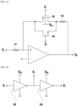
- FIG. 1A shows the structure of an amplifier according to the related art.
- the amplifier may include a first resistor 110 connected to the input terminal and a second resistor 120 connected to the output terminal.
- the input signal Vi input to the input terminal may be amplified through the first resistor 110 and the second resistor 120 and appear as an output signal Vo at the output terminal.
- the gain of the amplifier may be determined based on the ratio between the resistance value of the first resistor 110 and the resistance value of the second resistor 120.
- a switch may be electrically connected to one end of the second resistor 120 to turn the amplifier on or off or to change the gain of the amplifier.
- This switch may be implemented using a complementary metal-oxide semiconductor (CMOS) in which a p-type metal-oxide-semiconductor (PMOS) 130 and an n-type metal-oxide-semiconductor (NMOS) 140 are combined.
- CMOS complementary metal-oxide semiconductor
- PMOS p-type metal-oxide-semiconductor
- NMOS n-type metal-oxide-semiconductor
- both the PMOS 130 and the NMOS 140 may be turned on.
- V 1 is lower than the threshold voltage of the MOSFET, both the PMOS 130 and the NMOS 140 may be turned off. That is, turn-on/turn-off control of the switch including the PMOS 130 and the NMOS 140 may be achieved by controlling the V 1 voltage.
- MOSFET metal-oxide-semiconductor field-effect transistor
- FIG. 1B shows a switch control processor for controlling the switch of an amplifier according to the related art.
- the PMOS may be turned on when the voltage applied to the gate terminal is less than the threshold voltage
- the NMOS may be turned on when the voltage applied to the gate terminal exceeds the threshold voltage.
- the switch control processor for controlling the switch of the amplifier according to the related art may be configured as shown in FIG. 2B .
- the first inverter 150 may receive an input signal V 1 as input to the switch control processor and produce an output signal V 1 '.
- the signal V 1 ' output by the first inverter 150 is supplied to the gate terminal of the PMOS constituting the switch.
- the signal V 1 ' output by the first inverter 150 may be input to the second inverter 160, and the second inverter 160 may produce an output signal V 1 .
- the signal V 1 output by the second inverter 160 is supplied to the gate terminal of the NMOS constituting the switch.
- parasitic capacitance components may be generated between the gate terminal and the source terminal of the PMOS, between the gate terminal and the drain terminal of the PMOS, between the source terminal and the bulk terminal of the PMOS, and between the drain terminal and the bulk terminal of the PMOS.
- the fundamental signal to be amplified when the amplifier operates in a low frequency band, as the impedance of the parasitic capacitance components is sufficiently high, the fundamental signal to be amplified may not flow through the parasitic capacitance even when the switch is turned on.
- the amplifier when the amplifier operates in a very high frequency band such as the 5G mobile communication system, as the impedance value of the parasitic capacitance components becomes low, the fundamental signal to be amplified may flow through the parasitic capacitance when the switch is turned on. That is, in the related art, as a portion of the fundamental signal to be amplified may not flow to the output terminal of the amplifier but may flow through the parasitic capacitance, the gain of the amplifier can be reduced particularly in a high frequency range.
- FIG. 2A shows a switch control processor according to an embodiment of the disclosure.
- the switch control processor includes a first inverter 230 for receiving a control signal V 1 , a first CMOS where the gate terminal of the first PMOS 241 and the gate terminal of the first NMOS 242 are electrically connected to the output terminal of the first inverter 230, a second inverter 250 electrically connected to the output terminal of the first inverter 230, a second CMOS where the gate terminal of the second PMOS 251 and the gate terminal of the second NMOS 252 are electrically connected to the output terminal of the second inverter 250, a first impedance 210 electrically connected to the source terminal of the first PMOS 241 and the source terminal of the second PMOS 251 and having an impedance value higher than a first threshold value, and a second impedance 220 electrically connected to the source terminal of the first NMOS 242 and the source terminal of the second NMOS 252 and having an impedance value higher than the first threshold value.
- the output signal of the first inverter 230 may be zero.
- the first PMOS 241 may be turned on and the first NMOS 242 may be turned off.
- the output signal at the output terminal of the first CMOS may be set to V DD .
- the output signal from the output terminal of the first CMOS is used as a control signal for the gate terminal of the NMOS constituting the switch. That is, when V 1 is set to V DD , as the control signal supplied to the gate terminal of the NMOS constituting the switch is V DD , the NMOS may be turned on.
- the gate terminal of the NMOS when the NMOS constituting the switch is turned on, the gate terminal of the NMOS is electrically connected to the first impedance 210 having an impedance value higher than the first threshold value.
- the first impedance 210 may include a resistor and an inductor.
- the first impedance 210 having a high impedance value prevents a current from flowing through the parasitic capacitance between the gate terminal and the source terminal of the NMOS constituting the switch and through the parasitic capacitance between the gate terminal and the drain terminal of the NMOS constituting the switch. (The blocking effect of the current flowing through the parasitic capacitance will be described later with reference to FIG. 2B .)
- the output signal from the second inverter 250 may be V DD .
- the second PMOS 251 may be turned off and the second NMOS 252 may be turned on.
- the output signal from the output terminal of the second CMOS may be zero.
- the output signal from the output terminal of the second CMOS is used as a control signal for the gate terminal of the PMOS constituting the switch. That is, when 7 V 1 is set to V DD , as the control signal supplied to the gate terminal of the PMOS constituting the switch is 0, the PMOS may be turned on.
- the gate terminal of the PMOS is electrically connected to the second impedance 220 having an impedance value higher than the first threshold value.
- the second impedance 220 may include a resistor and an inductor.
- the second impedance 220 having a high impedance value prevents a current from flowing through the parasitic capacitance between the gate terminal and the source terminal of the PMOS constituting the switch and through the parasitic capacitance between the gate terminal and the drain terminal of the PMOS constituting the switch.
- the bulk terminal of the PMOS constituting the switch may be electrically connected to the source terminal of the first PMOS 241 or the source terminal of the second PMOS 251.
- the bulk terminal of the PMOS constituting the switch is electrically connected to the first impedance 210.
- the first impedance 210 may prevent a current from flowing through the parasitic capacitance between the bulk terminal and the source terminal of the PMOS constituting the switch and through the parasitic capacitance between the bulk terminal and the drain terminal of the PMOS constituting the switch.
- the bulk terminal of the NMOS constituting the switch may be electrically connected to the source terminal of the first NMOS 242 or the source terminal of the second NMOS 252.
- the bulk terminal of the NMOS constituting the switch is electrically connected to the second impedance 220.
- the second impedance 220 may prevent a current from flowing through the parasitic capacitance between the bulk terminal and the source terminal of the NMOS constituting the switch and through the parasitic capacitance between the bulk terminal and the drain terminal of the NMOS constituting the switch.
- the bulk terminal of the PMOS constituting the switch may be electrically connected to the V 2 node of the switch control processor, and the bulk terminal of the NMOS constituting the switch may be electrically connected to the V 3 node of the switch control processor.
- FIG. 2B illustrates an amplifier according to an embodiment of the disclosure.
- FIG. 2B illustrates an equivalent circuit when the MOSFET constituting the switch is turned on in the amplifier including the switch control processor shown in FIG. 2A .
- the switch is a CMOS including a PMOS and an NMOS.
- FIG. 2B illustrates a case where the switch includes only one PMOS, to avoid repeated descriptions.
- the source terminal s and the drain terminal d of the PMOS constituting the switch may be electrically connected through the resistor R sd,on .
- the resistor R sd,on may be generated between the drain terminal and the source terminal when the PMOS is turned on, and may have a low impedance value.
- a first parasitic capacitance component C gs may be generated between the gate terminal and the source terminal
- a second parasitic capacitance component C gd may be generated between the gate terminal and the drain terminal
- a third parasitic capacitance component C sb may be generated between the source terminal and the bulk terminal
- a fourth parasitic capacitance component C db may be generated between the drain terminal and the bulk terminal.
- the higher the operating frequency band of the amplifier the lower the impedance value of the parasitic capacitance component.
- the operating frequency band of the amplifier is sufficiently high such that the impedance value of the parasitic capacitor is less than or equal to a preset threshold, a portion of the fundamental signal to be amplified may flow through the parasitic capacitor.
- the fundamental signal may be amplified based on the ratio between the value of a first resistor 235 at the input stage of the amplifier and the value of a second resistor 240 at the output stage of the amplifier.
- a first impedance 210 having a high impedance value may be electrically connected to the bulk terminal of the MOSFET, and a second impedance 220 having a high impedance value may be electrically connected to the gate terminal of the MOSFET.
- current flows through the first parasitic capacitance component C gs and the second parasitic capacitance component C gd as the second impedance 220 having a high impedance value is connected to the gate terminal of the PMOS constituting the switch, the fundamental signal to be amplified may not flow through the gate terminal.
- the fundamental signal to be amplified may not flow through the bulk terminal.
- the gain of the amplifier may be increased by blocking the current flowing through the parasitic capacitor of the MOSFET constituting the switch by use of the first impedance 210 having a high impedance value and the second impedance 220 having a high impedance value.
- the first impedance 210 and the second impedance 220 may include a resistor or an inductor.
- the first impedance 210 and the second impedance 220 comprise a resistor having a high impedance value
- the current flowing through the parasitic capacitor of the MOSFET may be blocked regardless of the operating frequency of the amplifier.
- the first impedance 210 and the second impedance 220 comprise an inductor, as the impedance value of the inductor increases with the increasing operating frequency of the amplifier, the current flowing through the parasitic capacitor of the MOSFET can be blocked.
- FIG. 3A illustrates an amplifier including a two-stage switch and a short-circuit switch according to an example useful to understand the invention.
- the amount of amplifier feedback signal through the switch that is turned off may be increased. That is, the amount of the output signal fed back from the output terminal of the amplifier to the input terminal of the amplifier can increase.
- the bandwidth of the amplifier may be reduced due to the Miller effect.
- the switch may be configured in two stages, and a short-circuit switch may be disposed between the two switches.
- a two-stage switch may be disposed at the output terminal of the amplifier including a first resistor 310 at the input terminal and a second resistor 315 at the output terminal.
- the two-stage switch and the short-circuit switch may be controlled in a suitable manner so that the feedback signal of the amplifier can flow through the short-circuit switch.
- the two-stage switch constituting the amplifier may be configured by connecting a first switch, which includes a first CMOS based on a first PMOS 320 and a first NMOS 330, and a second switch, which includes a second CMOS based on a second PMOS 340 and a second NMOS 350, in series.
- the first switch and the second switch may operate in a manner identical or similar to that of the switch described with reference to FIG. 1A . For example, when V 1 and V 2 are set to V DD , all of the first PMOS 320, the first NMOS 330, the second PMOS 340, and the second NMOS 350 may be turned on.
- the short-circuit switch connected between the first switch and the second switch may include a third NMOS 361 and a fourth NMOS 362.
- the first switch and the second switch are turned on (i.e., when V 1 and V 2 are set to V DD )
- both the third NMOS 361 and the fourth NMOS 362 may be turned off.
- both the third NMOS 361 and the fourth NMOS 362 may be turned on. Even when the first switch and the second switch are turned off, the feedback signal may flow in the amplifier through the parasitic capacitor of the MOSFET. Most of the feedback signal passing through the second switch may flow to the short-circuit switch having a low impedance value. That is, according to an embodiment of the disclosure, most of the feedback signal passing through the second switch flows through the short-circuit switch, which prevents reduction of the bandwidth of the amplifier due to the feedback signal flowing to the input stage of the amplifier.
- FIG. 3B illustrates a switch control processor for controlling the two-stage switch according to an embodiment of the disclosure.
- the switch control processor may be divided into a first switch control processor for controlling the first switch constituting the two-stage switch and a second switch control processor for controlling the second switch.
- the first switch control processor for controlling the first switch may include a first inverter 371 for receiving a control signal V 1 , a first CMOS where the gate terminal of a first PMOS 391 and the gate terminal of a first NMOS 392 are electrically connected to the output terminal of the first inverter 371, a second inverter 372 electrically connected to the output terminal of the first inverter 371, a second CMOS where the gate terminal of a second PMOS 393 and the gate terminal of a second NMOS 394 are electrically connected to the output terminal of the second inverter 372, a first impedance 381 electrically connected to the source terminal of the first PMOS 391 and the source terminal of the second PMOS 393 and having an impedance value higher than a first threshold value, and a second impedance 3
- the output signal of the first inverter 371 when the control signal V 1 is set to V DD , the output signal of the first inverter 371 may be zero.
- the first PMOS 391 When the output signal of the first inverter 371 is 0, the first PMOS 391 may be turned on and the first NMOS 392 may be turned off.
- the output signal at the output terminal of the first CMOS may be V DD .
- the output signal at the output terminal of the first CMOS may be used as a control signal for the gate terminal of the NMOS constituting the switch. That is, when V 1 is set to V DD , as the control signal supplied to the gate terminal of the NMOS constituting the switch is V DD , the NMOS may be turned on.
- the gate terminal of the NMOS when the NMOS constituting the switch is turned on, the gate terminal of the NMOS may be electrically connected to the first impedance 381 having an impedance value higher than the first threshold value.
- the first impedance 381 may include a resistor and an inductor.
- the output signal of the second inverter 372 when the output signal of the first inverter 371 is set to 0, the output signal of the second inverter 372 may be V DD .
- the second PMOS 393 When the output signal of the second inverter 372 is V DD , the second PMOS 393 may be turned off and the second NMOS 394 may be turned on.
- the output signal at the output terminal of the second CMOS may be zero.
- the output signal at the output terminal of the second CMOS may be used as a control signal for the gate terminal of the PMOS constituting the switch. That is, when V 1 is set to V DD , as the control signal supplied to the gate terminal of the NMOS constituting the switch is 0, the PMOS may be turned on.
- the gate terminal of the PMOS when the PMOS constituting the switch is turned on, the gate terminal of the PMOS may be electrically connected to the second impedance 382 having an impedance value higher than the first threshold value.
- the second impedance 382 may include a resistor and an inductor.
- the bulk terminal of the PMOS constituting the first switch of the two-stage switch may be electrically connected to the source terminal of the first PMOS 391 or the source terminal (V 3 node) of the second PMOS in the switch control processor, and the bulk terminal of the NMOS constituting the first switch may be electrically connected to the source terminal of the first NMOS 392 or the source terminal (V 4 node) of the second NMOS 394.
- the second switch control processor for controlling the second switch may include a third CMOS where the gate terminal of a third PMOS 395 and the gate terminal of a third NMOS 396 are electrically connected to the output terminal of the first inverter 371, a fourth CMOS where the gate terminal of a fourth PMOS 397 and the gate terminal of a fourth NMOS 398 are electrically connected to the output terminal of the second inverter 372, a third impedance 383 electrically connected to the source terminal of the third PMOS 395 and the source terminal of the fourth PMOS 397 and having an impedance value higher than the first threshold value, and a fourth impedance 384 electrically connected to the source terminal of the third NMOS 396 and the source terminal of the fourth NMOS 398 and having an impedance value higher than the first threshold value.
- the bulk terminal of the PMOS constituting the second switch may be electrically connected to the source terminal of the third PMOS 395 or the source terminal (V 5 node) of the fourth PMOS 397, and the bulk terminal of the NMOS constituting the second switch may be electrically connected to the source terminal of the third NMOS 396 or the source terminal (V 6 node) of the fourth NMOS 398.
- the operation of the first switch control processor may be the same as or similar to the operation of the switch control processor described with reference to FIG. 2A .
- the operation of the second switch control processor may be the same as or similar to the operation of the first switch control processor described above.
- circuit diagrams shown in FIGS. 3A and 3B are only an embodiment of the disclosure, and the scope of the disclosure should not be limited to the circuit diagrams shown in FIGS. 3A and 3B .
- FIG. 4 illustrates a case where the short-circuit switch includes a PMOS and an NMOS according to an example useful to understand the invention.
- a two-stage switch may be disposed at the output terminal of the amplifier including a first resistor 410 at the input terminal and a second resistor 420 at the output terminal.
- the two-stage switch may include a first switch including a first CMOS based on a first PMOS 430 and a first NMOS 440, and a second switch including a second CMOS based on a second PMOS 450 and a second NMOS 460.
- a short-circuit switch including a third PMOS 470 and a third NMOS 480 may be disposed between the first switch and the second switch.
- V 1 and V 2 are set to V DD (i.e., when the first switch and the second switch are turned on)
- V 6 may be V DD .
- both the third PMOS 470 and the third NMOS 480 may be turned off.
- V 6 may be 0.
- both the third PMOS 470 and the third NMOS 480 may be turned on.
- the V 3 node which is the source terminals of the third PMOS 470 and the third NMOS 480, may have an impedance value lower than a preset threshold. Consequently, most of the feedback signal in the amplifier can flow through the short-circuit switch with a low impedance value.
- the voltage of the bulk terminal of the third PMOS 470 may be set to V 4
- the voltage of the bulk terminal of the third NMOS 480 may be set to V 5
- the bulk terminals of the third PMOS and the third NMOS constituting the short-circuit switch may be electrically connected to an impedance having a high impedance value as shown in FIG. 2B .
- FIG. 5 illustrates a variable gain amplifier according to an embodiment of the disclosure.
- the amplifier may include a first resistor 510 at the input terminal.
- a plurality of resistors 521, 522, and 523 may be connected in parallel to the output terminal, and switches 531, 532, and 533 corresponding respectively to the resistors 521, 522, and 523 may be disposed.
- the gain of the amplifier may be changed by controlling the turning on/off of each switch.
- the gain of the amplifier may be reduced due to the parasitic capacitance components of the switches connected in parallel as described above. Accordingly, the disclosure provides a switch control processor to prevent reduction of the gain of the amplifier due to the switch.
- the switch and switch control processor of the disclosure may be applied to each of the switches 531, 532 and 533 constituting the amplifier.
- the switch when configured as a two-stage switch in which a first switch and a second switch are connected in series and a short-circuit switch is placed between the first switch and the second switch, it is possible to reduce the amount of the feedback signal through the turned-off switch.
- the bandwidth of the amplifier can be increased by reducing the feedback signal that affects the input stage of the amplifier through the turned-off switch.
- an amplifier may include: a first resistor electrically connected to the input terminal; a second resistor electrically connected to the output terminal; a switch including a MOSFET and electrically connected to one end of the second resistor; and a switch control processor configured to electrically connect the gate terminal of the MOSFET constituting the switch and the bulk terminal of the MOSFET constituting the switch to an impedance having an impedance value higher than a preset first threshold.
- the switch may include a CMOS
- the switch control processor may include: a first impedance electrically connected to the gate terminal and the bulk terminal of the PMOS constituting the CMOS and having an impedance value higher than the first threshold; and a second impedance electrically connected to the gate terminal and the bulk terminal of the NMOS constituting the CMOS and having an impedance value higher than the first threshold.
- the switch control processor may include: a first inverter for receiving a control signal; a first CMOS in which the gate terminal of a first PMOS and the gate terminal of a first NMOS are electrically connected to the output terminal of the first inverter; a second inverter electrically connected to the output terminal of the first inverter; a second CMOS in which the gate terminal of a second PMOS and the gate terminal of a second NMOS are electrically connected to the output terminal of the second inverter; a first impedance electrically connected to the source terminal of the first PMOS and the source terminal of the second PMOS and having an impedance value higher than the first threshold; and a second impedance electrically connected to the source terminal of the first NMOS and the source terminal of the second NMOS and having an impedance value higher than the first threshold.
- the bulk terminal of the PMOS constituting the switch may be electrically connected to the source terminal of the first PMOS or the source terminal of the second PMOS, and the bulk terminal of the NMOS constituting the switch may be electrically connected to the source terminal of the first NMOS or the source terminal of the second NMOS.
- the gate terminal of the PMOS constituting the switch may be electrically connected to the output terminal of the first CMOS, and the gate terminal of the NMOS constituting the switch may be electrically connected to the output terminal of the second CMOS.
- the switch may include a first switch including a CMOS and electrically connected to one end of the second resistor, and a second switch including a CMOS and electrically connected to one end of the first switch.
- the switch control processor may include: a first inverter for receiving a control signal; a first CMOS in which the gate terminal of a first PMOS and the gate terminal of a first NMOS are electrically connected to the output terminal of the first inverter; a second inverter electrically connected to the output terminal of the first inverter; a second CMOS in which the gate terminal of a second PMOS and the gate terminal of a second NMOS are electrically connected to the output terminal of the second inverter; a first impedance electrically connected to the source terminal of the first PMOS and the source terminal of the second PMOS and having an impedance value higher than the first threshold; a second impedance electrically connected to the source terminal of the first NMOS and the source terminal of the second NMOS and having an impedance value higher than the first threshold; a third CMOS in which the gate terminal of a third PMOS and the gate terminal of a third NMOS are electrically connected to the output terminal of the first inverter;
- the bulk terminal of the PMOS constituting the first switch may be electrically connected to the source terminal of the first PMOS or the source terminal of the second PMOS
- the bulk terminal of the NMOS constituting the first switch may be electrically connected to the source terminal of the first NMOS or the source terminal of the second NMOS
- the bulk terminal of the PMOS constituting the second switch may be electrically connected to the source terminal of the third PMOS or the source terminal of the fourth PMOS
- the bulk terminal of the NMOS constituting the second switch may be electrically connected to the source terminal of the third NMOS or the source terminal of the fourth NMOS.
- the amplifier may further include a third switch having an impedance value lower than a preset second threshold between the first switch and the second switch.
- the third switch may include: a fifth PMOS having an impedance value lower than the second threshold and whose drain terminal is electrically connected between the PMOS constituting the first switch and the PMOS constituting the second switch; and a fifth NMOS having an impedance value lower than the second threshold and whose drain terminal is electrically connected between the NMOS constituting the first switch and the NMOS constituting the second switch.
- an electronic device may include an amplifier.
- the amplifier may include: a first resistor electrically connected to the input terminal; a second resistor electrically connected to the output terminal; a switch including a MOSFET and electrically connected to one end of the second resistor; and a switch control processor configured to electrically connect the gate terminal of the MOSFET constituting the switch and the bulk terminal of the MOSFET constituting the switch to an impedance having an impedance value higher than a preset first threshold.
- the switch may include a complementary metal-oxide semiconductor (CMOS), and the switch control processor may include: a first impedance electrically connected to the gate terminal and the bulk terminal of the PMOS constituting the CMOS and having an impedance value higher than the first threshold; and a second impedance electrically connected to the gate terminal and the bulk terminal of the NMOS constituting the CMOS and having an impedance value higher than the first threshold.
- CMOS complementary metal-oxide semiconductor
- the switch control processor includes: a first inverter for receiving a control signal; a first CMOS in which the gate terminal of a first PMOS and the gate terminal of a first NMOS are electrically connected to the output terminal of the first inverter; a second inverter electrically connected to the output terminal of the first inverter; a second CMOS in which the gate terminal of a second PMOS and the gate terminal of a second NMOS are electrically connected to the output terminal of the second inverter; a first impedance electrically connected to the source terminal of the first PMOS and the source terminal of the second PMOS and having an impedance value higher than the first threshold; and a second impedance electrically connected to the source terminal of the first NMOS and the source terminal of the second NMOS and having an impedance value higher than the first threshold.
- the bulk terminal of the PMOS constituting the switch may be electrically connected to the source terminal of the first PMOS or the source terminal of the second PMOS, and the bulk terminal of the NMOS constituting the switch may be electrically connected to the source terminal of the first NMOS or the source terminal of the second NMOS.
- the gate terminal of the PMOS constituting the switch may be electrically connected to the output terminal of the first CMOS, and the gate terminal of the NMOS constituting the switch may be electrically connected to the output terminal of the second CMOS.
- the switch may include a first switch including a CMOS and electrically connected to one end of the second resistor, and a second switch including a CMOS and electrically connected to one end of the first switch.
- the switch control processor includes: a first inverter for receiving a control signal; a first CMOS in which the gate terminal of a first PMOS and the gate terminal of a first NMOS are electrically connected to the output terminal of the first inverter; a second inverter electrically connected to the output terminal of the first inverter; a second CMOS in which the gate terminal of a second PMOS and the gate terminal of a second NMOS are electrically connected to the output terminal of the second inverter; a first impedance electrically connected to the source terminal of the first PMOS and the source terminal of the second PMOS and having an impedance value higher than the first threshold; a second impedance electrically connected to the source terminal of the first NMOS and the source terminal of the second NMOS and having an impedance value higher than the first threshold; a third CMOS in which the gate terminal of a third PMOS and the gate terminal of a third NMOS are electrically connected to the output terminal of the first inverter;
- the bulk terminal of the PMOS constituting the first switch may be electrically connected to the source terminal of the first PMOS or the source terminal of the second PMOS
- the bulk terminal of the NMOS constituting the first switch may be electrically connected to the source terminal of the first NMOS or the source terminal of the second NMOS
- the bulk terminal of the PMOS constituting the second switch may be electrically connected to the source terminal of the third PMOS or the source terminal of the fourth PMOS
- the bulk terminal of the NMOS constituting the second switch may be electrically connected to the source terminal of the third NMOS or the source terminal of the fourth NMOS.
- the amplifier may further include a third switch having an impedance value lower than a preset second threshold between the first switch and the second switch.
- the third switch may include: a fifth PMOS having an impedance value lower than the second threshold and whose drain terminal is electrically connected between the PMOS constituting the first switch and the PMOS constituting the second switch; and a fifth NMOS having an impedance value lower than the second threshold and whose drain terminal is electrically connected between the NMOS constituting the first switch and the NMOS constituting the second switch.
Landscapes
- Engineering & Computer Science (AREA)
- Power Engineering (AREA)
- Microelectronics & Electronic Packaging (AREA)
- Multimedia (AREA)
- Electronic Switches (AREA)
Description
- The disclosure relates to an amplifier that includes a plurality of switches and a switch control circuit to thereby adjust the gain.
- Since the commercial deployment of 4th generation (4G) communication systems, efforts have been made to develop improved 5th generation (5G) or pre-5G communication systems to meet the ever increasing demand for wireless data traffic. As such, 5G or pre-5G communication systems are also called "beyond 4G network" or "post long term evolution (LTE) system." To achieve higher data rates, 5G communication systems consider utilization of the mmWave band (e.g., 60 GHz band). To decrease path loss and increase the transmission distance in the mmWave band, various technologies including beamforming, massive multiple-input multiple-output (massive MIMO), full dimensional MIMO (FD-MIMO), array antennas, analog beamforming, and large scale antennas are considered for 5G communication systems. To improve system networks in 5G communication systems, technology development is under way regarding evolved small cells, advanced small cells, cloud radio access networks (cloud RANs), ultra-dense networks, device-to-device (D2D) communication, wireless backhaul, moving networks, cooperative communication, coordinated multi-points (CoMP), reception interference cancellation, and the like. In addition, advanced coding and modulation (ACM) schemes such as hybrid frequency shift keying (FSK) and quadrature amplitude modulation (QAM) (FQAM) and sliding window superposition coding (SWSC), and advanced access technologies such as filter bank multi carrier (FBMC), non-orthogonal multiple access (NOMA), and sparse code multiple access (SCMA) are also under development for 5G communication systems.
- Meanwhile, the Internet is evolving from a human centered network where humans create and consume information into the Internet of Things (IoT) where distributed elements or things process and exchange information. There has also emerged the Internet of Everything (IoE) technology that combines IoT technology with big data processing technology through connection with cloud servers. To realize IoT services, base technologies related to sensing, wired/wireless communication and network infrastructure, service interfacing, and security are needed, and technologies interconnecting things such as sensor networks, machine-to-machine (M2M) or machine type communication (MTC) are under development. In IoT environments, it is possible to provide intelligent Internet technology services, which collect and analyze data created by interconnected things to add new values to human life. Through convergence and combination between existing information technologies and various field technologies, IoT technology may be applied to various areas such as smart homes, smart buildings, smart cities, smart or connected cars, smart grids, health-care, smart consumer electronics, and advanced medical services.
- Accordingly, various attempts are being made to apply 5G communication systems to IoT networks. For example, sensor networks and machine-to-machine or machine type communication are being realized by use of 5G communication technologies including beamforming, MIMO, and array antennas. Application of cloud RANs to big data processing described above may be an instance of convergence of 5G communication technology and IoT technology.
- Document
WO 2018/045298 discloses a programmable gain amplifier in which a low capacitance analog switch circuit is implemented. DocumentUS 2013/0154740 A1 and document Xiaobin Shen Et Al; titled "A 0.25dB Gain Step High Linear Programmable Gain Amplifier"; XP32120605A; 25 October 2011, disclose conventional linear Programmable Gain Amplifier. DocumentWO 2014/011510 discloses a radio-frequency (RF) switch circuit implementing a Field-Effect-Transistor (FET). - The above information is presented as background information only to assist with an understanding of the disclosure. No determination has been made, and no assertion is made, as to whether any of the above might be applicable as prior art with regard to the disclosure.
- Aspects of the disclosure are to address at least the above-mentioned problems and/or disadvantages and to provide at least the advantages described below. Accordingly, an aspect of the disclosure is to provide an apparatus to change the gain of an amplifier including a resistor element. A plurality of switches may be required, and each switch may be implemented using a metal-oxide-semiconductor field-effect transistor (MOSFET). Meanwhile, in a 5G mobile communication system using the mmWave band, the performance (e.g., gain or bandwidth) of the amplifier may be reduced due to parasitic capacitance components caused by the MOSFETs. Accordingly, there is a need for an amplifier structure that can solve this problem.
- Additional aspects will be set forth in part in the description which follows and, in part, will be apparent from the description, or may be learned by practice of the presented embodiments.
- In accordance with an aspect of the disclosure, an amplifier is provided as defined by appended set of claims.
- In accordance with another aspect of the disclosure, an electronic device having an amplifier is provided as defined by appended set of claims.
- Other aspects, advantages, and salient features of the disclosure will become apparent to those skilled in the art from the following detailed description, which, taken in conjunction with the annexed drawings, discloses various embodiments of the disclosure.
- According to an embodiment of the disclosure, it is possible to prevent reduction of the gain of the amplifier due to the parasitic capacitance caused by the MOSFET constituting the switch. In addition, it is possible to prevent reduction of the bandwidth of the amplifier due to the Miller effect.
- The above and other aspects, features and advantages of certain embodiments of the disclosure will be more apparent from the following description, taken in conjunction with the accompanying drawings, in which:
-
FIG. 1A shows the structure of an amplifier according to the related art; -
FIG. 1B shows a switch control processor for controlling the switch of an amplifier according to the related art; -
FIG. 2A shows a switch control processor according to a claimed embodiment of the disclosure; -
FIG. 2B illustrates an amplifier according to an embodiment of the disclosure; -
FIG. 3A illustrates an amplifier including a two-stage switch and a short-circuit switch according to an example useful to understand the invention. -
FIG. 3B illustrates a switch control processor for controlling the two-stage switch and the short-circuit switch according to an embodiment of the disclosure; -
FIG. 4 illustrates a case where the short-circuit switch includes a p-type metal-oxide-semiconductor (PMOS) and an n-type metal-oxide-semiconductor (NMOS) according to an example useful to understand the invention; and -
FIG. 5 illustrates a variable gain amplifier according to an example useful to understand the invention. - Throughout the drawings, like reference numerals will be understood to refer to like parts, components, and structures.
- The following description with reference to the accompanying drawings is provided to assist in a comprehensive understanding of various embodiments of the disclosure as defined by the claims. It includes various specific details to assist in that understanding but these are to be regarded as merely exemplary. Accordingly, those of ordinary skill in the art will recognize that various changes and modifications of the various embodiments described herein can be made without departing from the scope of the disclosure. In addition, descriptions of well-known functions and constructions may be omitted for clarity and conciseness.
- The terms and words used in the following description and claims are not limited to the bibliographical meanings, but, are merely used by the inventor to enable a clear and consistent understanding of the disclosure. Accordingly, it should be apparent to those skilled in the art that the following description of various embodiments of the disclosure is provided for illustration purpose only and not for the purpose of limiting the disclosure as defined by the appended claims.
- It is to be understood that the singular forms "a," "an," and "the" include plural referents unless the context clearly dictates otherwise. Thus, for example, reference to "a component surface" includes reference to one or more of such surfaces.
- In the drawings, some elements are exaggerated, omitted, or only outlined in brief, and thus may be not drawn to scale. The same or similar reference symbols are used throughout the drawings to refer to the same or like parts.
- The aspects, features, and advantages of certain embodiments of the disclosure will be more apparent from the following detailed description taken in conjunction with the accompanying drawings. The description of the various embodiments is to be construed as exemplary only and does not describe every possible instance of the disclosure. It should be apparent to those skilled in the art that the following description of various embodiments of the disclosure is provided for illustrative purposes only and not for the purpose of limiting the disclosure as defined by the appended claims. The same reference symbols are used throughout the description to refer to the same parts.
- Meanwhile, it is known to those skilled in the art that blocks of a flowchart (or sequence diagram) and a combination of flowcharts may be represented and executed by computer program instructions. These computer program instructions may be loaded on a processor of a general purpose computer, special purpose computer, or programmable data processing equipment. When the loaded program instructions are executed by the processor, they create a means for carrying out functions described in the flowchart. As the computer program instructions may be stored in a computer readable memory that is usable in a specialized computer or a programmable data processing equipment, it is also possible to create articles of manufacture that carry out functions described in the flowchart. As the computer program instructions may be loaded on a computer or a programmable data processing equipment, when executed as processes, they may carry out operations of functions described in the flowchart.
- A block of a flowchart may correspond to a module, a segment or a code containing one or more executable instructions implementing one or more logical functions, or to a part thereof. In some cases, functions described by blocks may be executed in an order different from the listed order. For example, two blocks listed in sequence may be executed at the same time or executed in reverse order.
- In the description, the word "unit," "module," or the like may refer to a software component or hardware component such as a field-programmable gate array (FPGA) or an application-specific integrated circuit (ASIC) capable of carrying out a function or an operation. However, "unit" or the like is not limited to hardware or software. A unit or the like may be configured so as to reside in an addressable storage medium or to drive one or more processors. Units or the like may refer to software components, object-oriented software components, class components, task components, processes, functions, attributes, procedures, subroutines, program code segments, drivers, firmware, microcode, circuits, data, databases, data structures, tables, arrays, or variables. A function provided by a component and unit may be a combination of smaller components and units, and it may be combined with others to compose large components and units. Components and units may be configured to drive a device or one or more processors in a secure multimedia card. In a certain embodiment, a unit or the like may include at least one processor.
-
FIG. 1A shows the structure of an amplifier according to the related art. - Referring to
FIG. 1A , in the related art, the amplifier may include afirst resistor 110 connected to the input terminal and asecond resistor 120 connected to the output terminal. The input signal Vi input to the input terminal may be amplified through thefirst resistor 110 and thesecond resistor 120 and appear as an output signal Vo at the output terminal. The gain of the amplifier may be determined based on the ratio between the resistance value of thefirst resistor 110 and the resistance value of thesecond resistor 120. - In the related art, a switch may be electrically connected to one end of the
second resistor 120 to turn the amplifier on or off or to change the gain of the amplifier. This switch may be implemented using a complementary metal-oxide semiconductor (CMOS) in which a p-type metal-oxide-semiconductor (PMOS) 130 and an n-type metal-oxide-semiconductor (NMOS) 140 are combined. - According to the related art, when V1 is higher than the threshold voltage of the metal-oxide-semiconductor field-effect transistor (MOSFET), both the
PMOS 130 and theNMOS 140 may be turned on. When V1 is lower than the threshold voltage of the MOSFET, both thePMOS 130 and theNMOS 140 may be turned off. That is, turn-on/turn-off control of the switch including thePMOS 130 and theNMOS 140 may be achieved by controlling the V1 voltage. -
FIG. 1B shows a switch control processor for controlling the switch of an amplifier according to the related art. - Referring to
FIG. 1B , in the related art, the PMOS may be turned on when the voltage applied to the gate terminal is less than the threshold voltage, and the NMOS may be turned on when the voltage applied to the gate terminal exceeds the threshold voltage. Hence, the switch control processor for controlling the switch of the amplifier according to the related art may be configured as shown inFIG. 2B . - In the related art, the
first inverter 150 may receive an input signal V1 as input to the switch control processor and produce an output signal V1'. The signal V1' output by thefirst inverter 150 is supplied to the gate terminal of the PMOS constituting the switch. The signal V1' output by thefirst inverter 150 may be input to thesecond inverter 160, and thesecond inverter 160 may produce an output signal V1. The signal V1 output by thesecond inverter 160 is supplied to the gate terminal of the NMOS constituting the switch. - In the related art, due to the characteristic of the MOSFETs, parasitic capacitance components may be generated between the gate terminal and the source terminal of the PMOS, between the gate terminal and the drain terminal of the PMOS, between the source terminal and the bulk terminal of the PMOS, and between the drain terminal and the bulk terminal of the PMOS.
- According to the related art, when the amplifier operates in a low frequency band, as the impedance of the parasitic capacitance components is sufficiently high, the fundamental signal to be amplified may not flow through the parasitic capacitance even when the switch is turned on. However, when the amplifier operates in a very high frequency band such as the 5G mobile communication system, as the impedance value of the parasitic capacitance components becomes low, the fundamental signal to be amplified may flow through the parasitic capacitance when the switch is turned on. That is, in the related art, as a portion of the fundamental signal to be amplified may not flow to the output terminal of the amplifier but may flow through the parasitic capacitance, the gain of the amplifier can be reduced particularly in a high frequency range.
-
FIG. 2A shows a switch control processor according to an embodiment of the disclosure. - Referring to
FIG. 2A , in one embodiment, the switch control processor includes afirst inverter 230 for receiving a control signal V1, a first CMOS where the gate terminal of thefirst PMOS 241 and the gate terminal of thefirst NMOS 242 are electrically connected to the output terminal of thefirst inverter 230, asecond inverter 250 electrically connected to the output terminal of thefirst inverter 230, a second CMOS where the gate terminal of thesecond PMOS 251 and the gate terminal of thesecond NMOS 252 are electrically connected to the output terminal of thesecond inverter 250, afirst impedance 210 electrically connected to the source terminal of thefirst PMOS 241 and the source terminal of thesecond PMOS 251 and having an impedance value higher than a first threshold value, and asecond impedance 220 electrically connected to the source terminal of thefirst NMOS 242 and the source terminal of thesecond NMOS 252 and having an impedance value higher than the first threshold value. - In one embodiment, when the control signal V1 is set to VDD, the output signal of the
first inverter 230 may be zero. When the output signal of thefirst inverter 230 is 0, thefirst PMOS 241 may be turned on and thefirst NMOS 242 may be turned off. When only thefirst PMOS 241 is turned on, the output signal at the output terminal of the first CMOS may be set to VDD. The output signal from the output terminal of the first CMOS is used as a control signal for the gate terminal of the NMOS constituting the switch. That is, when V1 is set to VDD, as the control signal supplied to the gate terminal of the NMOS constituting the switch is VDD, the NMOS may be turned on. - In one embodiment, when the NMOS constituting the switch is turned on, the gate terminal of the NMOS is electrically connected to the
first impedance 210 having an impedance value higher than the first threshold value. In various embodiments, thefirst impedance 210 may include a resistor and an inductor. - According to the invention, the
first impedance 210 having a high impedance value prevents a current from flowing through the parasitic capacitance between the gate terminal and the source terminal of the NMOS constituting the switch and through the parasitic capacitance between the gate terminal and the drain terminal of the NMOS constituting the switch. (The blocking effect of the current flowing through the parasitic capacitance will be described later with reference toFIG. 2B .) - In one embodiment, when the output signal from the
first inverter 230 is 0, the output signal from thesecond inverter 250 may be VDD. When the output signal of thesecond inverter 250 is VDD, thesecond PMOS 251 may be turned off and thesecond NMOS 252 may be turned on. When only thesecond NMOS 252 is turned on, the output signal from the output terminal of the second CMOS may be zero. The output signal from the output terminal of the second CMOS is used as a control signal for the gate terminal of the PMOS constituting the switch. That is, when 7 V1 is set to VDD, as the control signal supplied to the gate terminal of the PMOS constituting the switch is 0, the PMOS may be turned on. - In one embodiment, when the PMOS constituting the switch is turned on, the gate terminal of the PMOS is electrically connected to the
second impedance 220 having an impedance value higher than the first threshold value. In various embodiments, thesecond impedance 220 may include a resistor and an inductor. - According to the invention, the
second impedance 220 having a high impedance value prevents a current from flowing through the parasitic capacitance between the gate terminal and the source terminal of the PMOS constituting the switch and through the parasitic capacitance between the gate terminal and the drain terminal of the PMOS constituting the switch. - In one embodiment, the bulk terminal of the PMOS constituting the switch may be electrically connected to the source terminal of the
first PMOS 241 or the source terminal of thesecond PMOS 251. The bulk terminal of the PMOS constituting the switch is electrically connected to thefirst impedance 210. Hence, thefirst impedance 210 may prevent a current from flowing through the parasitic capacitance between the bulk terminal and the source terminal of the PMOS constituting the switch and through the parasitic capacitance between the bulk terminal and the drain terminal of the PMOS constituting the switch. - In one embodiment, the bulk terminal of the NMOS constituting the switch may be electrically connected to the source terminal of the
first NMOS 242 or the source terminal of thesecond NMOS 252. The bulk terminal of the NMOS constituting the switch is electrically connected to thesecond impedance 220. Hence, thesecond impedance 220 may prevent a current from flowing through the parasitic capacitance between the bulk terminal and the source terminal of the NMOS constituting the switch and through the parasitic capacitance between the bulk terminal and the drain terminal of the NMOS constituting the switch. - In one embodiment, the bulk terminal of the PMOS constituting the switch may be electrically connected to the V2 node of the switch control processor, and the bulk terminal of the NMOS constituting the switch may be electrically connected to the V3 node of the switch control processor.
-
FIG. 2B illustrates an amplifier according to an embodiment of the disclosure. - More specifically,
FIG. 2B illustrates an equivalent circuit when the MOSFET constituting the switch is turned on in the amplifier including the switch control processor shown inFIG. 2A . - Referring to
FIG. 2A , the switch is a CMOS including a PMOS and an NMOS.FIG. 2B illustrates a case where the switch includes only one PMOS, to avoid repeated descriptions. - Referring to
FIG. 2B , in one embodiment, when the switch is turned on, the source terminal s and the drain terminal d of the PMOS constituting the switch may be electrically connected through the resistor Rsd,on. For example, the resistor Rsd,on may be generated between the drain terminal and the source terminal when the PMOS is turned on, and may have a low impedance value. Due to the characteristics of the MOSFET, a first parasitic capacitance component Cgs may be generated between the gate terminal and the source terminal, a second parasitic capacitance component Cgd may be generated between the gate terminal and the drain terminal, a third parasitic capacitance component Csb may be generated between the source terminal and the bulk terminal, and a fourth parasitic capacitance component Cdb may be generated between the drain terminal and the bulk terminal. - In one embodiment, the higher the operating frequency band of the amplifier, the lower the impedance value of the parasitic capacitance component. When the operating frequency band of the amplifier is sufficiently high such that the impedance value of the parasitic capacitor is less than or equal to a preset threshold, a portion of the fundamental signal to be amplified may flow through the parasitic capacitor. In one embodiment, the fundamental signal may be amplified based on the ratio between the value of a
first resistor 235 at the input stage of the amplifier and the value of asecond resistor 240 at the output stage of the amplifier. - In one embodiment, a
first impedance 210 having a high impedance value may be electrically connected to the bulk terminal of the MOSFET, and asecond impedance 220 having a high impedance value may be electrically connected to the gate terminal of the MOSFET. Although current flows through the first parasitic capacitance component Cgs and the second parasitic capacitance component Cgd, as thesecond impedance 220 having a high impedance value is connected to the gate terminal of the PMOS constituting the switch, the fundamental signal to be amplified may not flow through the gate terminal. Similarly, although current flows through the third parasitic capacitance component Csb and the fourth parasitic capacitance component Cdb, as thefirst impedance 210 having a high impedance value is connected to the bulk terminal of the PMOS constituting the switch, the fundamental signal to be amplified may not flow through the bulk terminal. - In other words, according to an embodiment of the disclosure, the gain of the amplifier may be increased by blocking the current flowing through the parasitic capacitor of the MOSFET constituting the switch by use of the
first impedance 210 having a high impedance value and thesecond impedance 220 having a high impedance value. - In one embodiment, the
first impedance 210 and thesecond impedance 220 may include a resistor or an inductor. When thefirst impedance 210 and thesecond impedance 220 comprise a resistor having a high impedance value, the current flowing through the parasitic capacitor of the MOSFET may be blocked regardless of the operating frequency of the amplifier. When thefirst impedance 210 and thesecond impedance 220 comprise an inductor, as the impedance value of the inductor increases with the increasing operating frequency of the amplifier, the current flowing through the parasitic capacitor of the MOSFET can be blocked. -
FIG. 3A illustrates an amplifier including a two-stage switch and a short-circuit switch according to an example useful to understand the invention. - Referring to
FIG. 3A , in one example, when increasing the impedance of the gate and bulk terminals of the MOSFETs constituting the switch, the amount of amplifier feedback signal through the switch that is turned off may be increased. That is, the amount of the output signal fed back from the output terminal of the amplifier to the input terminal of the amplifier can increase. When the amount of the amplifier feedback signal increases, the bandwidth of the amplifier may be reduced due to the Miller effect. - In one example, to prevent the bandwidth reduction effect due to the increased feedback signal through the turned-off switch, as shown in
FIG. 3A , the switch may be configured in two stages, and a short-circuit switch may be disposed between the two switches. In an embodiment, a two-stage switch may be disposed at the output terminal of the amplifier including afirst resistor 310 at the input terminal and asecond resistor 315 at the output terminal. In various embodiments, the two-stage switch and the short-circuit switch may be controlled in a suitable manner so that the feedback signal of the amplifier can flow through the short-circuit switch. - In one example, the two-stage switch constituting the amplifier may be configured by connecting a first switch, which includes a first CMOS based on a
first PMOS 320 and afirst NMOS 330, and a second switch, which includes a second CMOS based on asecond PMOS 340 and asecond NMOS 350, in series. The first switch and the second switch may operate in a manner identical or similar to that of the switch described with reference toFIG. 1A . For example, when V1 and V2 are set to VDD, all of thefirst PMOS 320, thefirst NMOS 330, thesecond PMOS 340, and thesecond NMOS 350 may be turned on. - In one example, the short-circuit switch connected between the first switch and the second switch may include a
third NMOS 361 and afourth NMOS 362. When the first switch and the second switch are turned on (i.e., when V1 and V2 are set to VDD), both thethird NMOS 361 and thefourth NMOS 362 may be turned off. - In one example, when the first switch and the second switch are turned off (i.e., when V1 and V2 are set to 0), both the
third NMOS 361 and thefourth NMOS 362 may be turned on. Even when the first switch and the second switch are turned off, the feedback signal may flow in the amplifier through the parasitic capacitor of the MOSFET. Most of the feedback signal passing through the second switch may flow to the short-circuit switch having a low impedance value. That is, according to an embodiment of the disclosure, most of the feedback signal passing through the second switch flows through the short-circuit switch, which prevents reduction of the bandwidth of the amplifier due to the feedback signal flowing to the input stage of the amplifier. -
FIG. 3B illustrates a switch control processor for controlling the two-stage switch according to an embodiment of the disclosure. - Referring to
FIG. 3B , in one embodiment, the switch control processor may be divided into a first switch control processor for controlling the first switch constituting the two-stage switch and a second switch control processor for controlling the second switch. The first switch control processor for controlling the first switch may include afirst inverter 371 for receiving a control signal V1, a first CMOS where the gate terminal of afirst PMOS 391 and the gate terminal of afirst NMOS 392 are electrically connected to the output terminal of thefirst inverter 371, asecond inverter 372 electrically connected to the output terminal of thefirst inverter 371, a second CMOS where the gate terminal of asecond PMOS 393 and the gate terminal of asecond NMOS 394 are electrically connected to the output terminal of thesecond inverter 372, afirst impedance 381 electrically connected to the source terminal of thefirst PMOS 391 and the source terminal of thesecond PMOS 393 and having an impedance value higher than a first threshold value, and asecond impedance 382 electrically connected to the source terminal of thefirst NMOS 392 and the source terminal of thesecond NMOS 394 and having an impedance value higher than the first threshold value. - In one embodiment, when the control signal V1 is set to VDD, the output signal of the
first inverter 371 may be zero. When the output signal of thefirst inverter 371 is 0, thefirst PMOS 391 may be turned on and thefirst NMOS 392 may be turned off. When only thefirst PMOS 391 is turned on, the output signal at the output terminal of the first CMOS may be VDD. The output signal at the output terminal of the first CMOS may be used as a control signal for the gate terminal of the NMOS constituting the switch. That is, when V1 is set to VDD, as the control signal supplied to the gate terminal of the NMOS constituting the switch is VDD, the NMOS may be turned on. - In one embodiment, when the NMOS constituting the switch is turned on, the gate terminal of the NMOS may be electrically connected to the
first impedance 381 having an impedance value higher than the first threshold value. Thefirst impedance 381 may include a resistor and an inductor. - In one embodiment, when the output signal of the
first inverter 371 is set to 0, the output signal of thesecond inverter 372 may be VDD. When the output signal of thesecond inverter 372 is VDD, thesecond PMOS 393 may be turned off and thesecond NMOS 394 may be turned on. When only thesecond NMOS 394 is turned on, the output signal at the output terminal of the second CMOS may be zero. The output signal at the output terminal of the second CMOS may be used as a control signal for the gate terminal of the PMOS constituting the switch. That is, when V1 is set to VDD, as the control signal supplied to the gate terminal of the NMOS constituting the switch is 0, the PMOS may be turned on. - In one embodiment, when the PMOS constituting the switch is turned on, the gate terminal of the PMOS may be electrically connected to the
second impedance 382 having an impedance value higher than the first threshold value. Thesecond impedance 382 may include a resistor and an inductor. - In one embodiment, the bulk terminal of the PMOS constituting the first switch of the two-stage switch may be electrically connected to the source terminal of the
first PMOS 391 or the source terminal (V3 node) of the second PMOS in the switch control processor, and the bulk terminal of the NMOS constituting the first switch may be electrically connected to the source terminal of thefirst NMOS 392 or the source terminal (V4 node) of thesecond NMOS 394. - In one embodiment, the second switch control processor for controlling the second switch may include a third CMOS where the gate terminal of a
third PMOS 395 and the gate terminal of athird NMOS 396 are electrically connected to the output terminal of thefirst inverter 371, a fourth CMOS where the gate terminal of afourth PMOS 397 and the gate terminal of afourth NMOS 398 are electrically connected to the output terminal of thesecond inverter 372, athird impedance 383 electrically connected to the source terminal of thethird PMOS 395 and the source terminal of thefourth PMOS 397 and having an impedance value higher than the first threshold value, and afourth impedance 384 electrically connected to the source terminal of thethird NMOS 396 and the source terminal of thefourth NMOS 398 and having an impedance value higher than the first threshold value. The bulk terminal of the PMOS constituting the second switch may be electrically connected to the source terminal of thethird PMOS 395 or the source terminal (V5 node) of thefourth PMOS 397, and the bulk terminal of the NMOS constituting the second switch may be electrically connected to the source terminal of thethird NMOS 396 or the source terminal (V6 node) of thefourth NMOS 398. - In one embodiment, the operation of the first switch control processor may be the same as or similar to the operation of the switch control processor described with reference to
FIG. 2A . The operation of the second switch control processor may be the same as or similar to the operation of the first switch control processor described above. - Meanwhile, the circuit diagrams shown in
FIGS. 3A and3B are only an embodiment of the disclosure, and the scope of the disclosure should not be limited to the circuit diagrams shown inFIGS. 3A and3B . -
FIG. 4 illustrates a case where the short-circuit switch includes a PMOS and an NMOS according to an example useful to understand the invention. - Referring to
FIG. 4 , in one example, a two-stage switch may be disposed at the output terminal of the amplifier including afirst resistor 410 at the input terminal and asecond resistor 420 at the output terminal. The two-stage switch may include a first switch including a first CMOS based on afirst PMOS 430 and afirst NMOS 440, and a second switch including a second CMOS based on asecond PMOS 450 and asecond NMOS 460. - In one example, a short-circuit switch including a
third PMOS 470 and athird NMOS 480 may be disposed between the first switch and the second switch. When V1 and V2 are set to VDD (i.e., when the first switch and the second switch are turned on), V6 may be VDD. In other words, when the first switch and the second switch are turned on, both thethird PMOS 470 and thethird NMOS 480 may be turned off. - In one example, When V1 and V2 are set to 0 (i.e., when the first switch and the second switch are turned off), V6 may be 0. In other words, when the first switch and the second switch are turned off, both the
third PMOS 470 and thethird NMOS 480 may be turned on. The V3 node, which is the source terminals of thethird PMOS 470 and thethird NMOS 480, may have an impedance value lower than a preset threshold. Consequently, most of the feedback signal in the amplifier can flow through the short-circuit switch with a low impedance value. - In one example, the voltage of the bulk terminal of the
third PMOS 470 may be set to V4, and the voltage of the bulk terminal of thethird NMOS 480 may be set to V5. The bulk terminals of the third PMOS and the third NMOS constituting the short-circuit switch may be electrically connected to an impedance having a high impedance value as shown inFIG. 2B . -
FIG. 5 illustrates a variable gain amplifier according to an embodiment of the disclosure. - Referring to
FIG. 5 , in one example, the amplifier may include afirst resistor 510 at the input terminal. To vary the gain of the amplifier, a plurality ofresistors resistors - In one example, when the
switches switches - In addition, according to an example, when the switch is configured as a two-stage switch in which a first switch and a second switch are connected in series and a short-circuit switch is placed between the first switch and the second switch, it is possible to reduce the amount of the feedback signal through the turned-off switch. Hence, the bandwidth of the amplifier can be increased by reducing the feedback signal that affects the input stage of the amplifier through the turned-off switch.
- According to various embodiments of the disclosure, an amplifier may include: a first resistor electrically connected to the input terminal; a second resistor electrically connected to the output terminal; a switch including a MOSFET and electrically connected to one end of the second resistor; and a switch control processor configured to electrically connect the gate terminal of the MOSFET constituting the switch and the bulk terminal of the MOSFET constituting the switch to an impedance having an impedance value higher than a preset first threshold.
- In one embodiment, the switch may include a CMOS, and the switch control processor may include: a first impedance electrically connected to the gate terminal and the bulk terminal of the PMOS constituting the CMOS and having an impedance value higher than the first threshold; and a second impedance electrically connected to the gate terminal and the bulk terminal of the NMOS constituting the CMOS and having an impedance value higher than the first threshold.
- In one embodiment, the switch control processor may include: a first inverter for receiving a control signal; a first CMOS in which the gate terminal of a first PMOS and the gate terminal of a first NMOS are electrically connected to the output terminal of the first inverter; a second inverter electrically connected to the output terminal of the first inverter; a second CMOS in which the gate terminal of a second PMOS and the gate terminal of a second NMOS are electrically connected to the output terminal of the second inverter; a first impedance electrically connected to the source terminal of the first PMOS and the source terminal of the second PMOS and having an impedance value higher than the first threshold; and a second impedance electrically connected to the source terminal of the first NMOS and the source terminal of the second NMOS and having an impedance value higher than the first threshold.
- In one embodiment, the bulk terminal of the PMOS constituting the switch may be electrically connected to the source terminal of the first PMOS or the source terminal of the second PMOS, and the bulk terminal of the NMOS constituting the switch may be electrically connected to the source terminal of the first NMOS or the source terminal of the second NMOS.
- In one embodiment, the gate terminal of the PMOS constituting the switch may be electrically connected to the output terminal of the first CMOS, and the gate terminal of the NMOS constituting the switch may be electrically connected to the output terminal of the second CMOS.
- In one embodiment, the switch may include a first switch including a CMOS and electrically connected to one end of the second resistor, and a second switch including a CMOS and electrically connected to one end of the first switch.
- In one embodiment, the switch control processor may include: a first inverter for receiving a control signal; a first CMOS in which the gate terminal of a first PMOS and the gate terminal of a first NMOS are electrically connected to the output terminal of the first inverter; a second inverter electrically connected to the output terminal of the first inverter; a second CMOS in which the gate terminal of a second PMOS and the gate terminal of a second NMOS are electrically connected to the output terminal of the second inverter; a first impedance electrically connected to the source terminal of the first PMOS and the source terminal of the second PMOS and having an impedance value higher than the first threshold; a second impedance electrically connected to the source terminal of the first NMOS and the source terminal of the second NMOS and having an impedance value higher than the first threshold; a third CMOS in which the gate terminal of a third PMOS and the gate terminal of a third NMOS are electrically connected to the output terminal of the first inverter; a fourth CMOS in which the gate terminal of a fourth PMOS and the gate terminal of a fourth NMOS are electrically connected to the output terminal of the second inverter; a third impedance electrically connected to the source terminal of the third PMOS and the source terminal of the fourth PMOS and having an impedance value higher than the first threshold; and a fourth impedance electrically connected to the source terminal of the third NMOS and the source terminal of the fourth NMOS and having an impedance value higher than the first threshold.
- In one embodiment, the bulk terminal of the PMOS constituting the first switch may be electrically connected to the source terminal of the first PMOS or the source terminal of the second PMOS, the bulk terminal of the NMOS constituting the first switch may be electrically connected to the source terminal of the first NMOS or the source terminal of the second NMOS, the bulk terminal of the PMOS constituting the second switch may be electrically connected to the source terminal of the third PMOS or the source terminal of the fourth PMOS, and the bulk terminal of the NMOS constituting the second switch may be electrically connected to the source terminal of the third NMOS or the source terminal of the fourth NMOS.
- In one embodiment, the amplifier may further include a third switch having an impedance value lower than a preset second threshold between the first switch and the second switch.
- In one embodiment, the third switch may include: a fifth PMOS having an impedance value lower than the second threshold and whose drain terminal is electrically connected between the PMOS constituting the first switch and the PMOS constituting the second switch; and a fifth NMOS having an impedance value lower than the second threshold and whose drain terminal is electrically connected between the NMOS constituting the first switch and the NMOS constituting the second switch.
- According to various embodiments of the disclosure, an electronic device may include an amplifier. The amplifier may include: a first resistor electrically connected to the input terminal; a second resistor electrically connected to the output terminal; a switch including a MOSFET and electrically connected to one end of the second resistor; and a switch control processor configured to electrically connect the gate terminal of the MOSFET constituting the switch and the bulk terminal of the MOSFET constituting the switch to an impedance having an impedance value higher than a preset first threshold.
- In one embodiment, the switch may include a complementary metal-oxide semiconductor (CMOS), and the switch control processor may include: a first impedance electrically connected to the gate terminal and the bulk terminal of the PMOS constituting the CMOS and having an impedance value higher than the first threshold; and a second impedance electrically connected to the gate terminal and the bulk terminal of the NMOS constituting the CMOS and having an impedance value higher than the first threshold.
- According to the invention, the switch control processor includes: a first inverter for receiving a control signal; a first CMOS in which the gate terminal of a first PMOS and the gate terminal of a first NMOS are electrically connected to the output terminal of the first inverter; a second inverter electrically connected to the output terminal of the first inverter; a second CMOS in which the gate terminal of a second PMOS and the gate terminal of a second NMOS are electrically connected to the output terminal of the second inverter; a first impedance electrically connected to the source terminal of the first PMOS and the source terminal of the second PMOS and having an impedance value higher than the first threshold; and a second impedance electrically connected to the source terminal of the first NMOS and the source terminal of the second NMOS and having an impedance value higher than the first threshold.
- In one embodiment, the bulk terminal of the PMOS constituting the switch may be electrically connected to the source terminal of the first PMOS or the source terminal of the second PMOS, and the bulk terminal of the NMOS constituting the switch may be electrically connected to the source terminal of the first NMOS or the source terminal of the second NMOS.
- In one embodiment, the gate terminal of the PMOS constituting the switch may be electrically connected to the output terminal of the first CMOS, and the gate terminal of the NMOS constituting the switch may be electrically connected to the output terminal of the second CMOS.
- In one embodiment, the switch may include a first switch including a CMOS and electrically connected to one end of the second resistor, and a second switch including a CMOS and electrically connected to one end of the first switch.
- According to the invention, the switch control processor includes: a first inverter for receiving a control signal; a first CMOS in which the gate terminal of a first PMOS and the gate terminal of a first NMOS are electrically connected to the output terminal of the first inverter; a second inverter electrically connected to the output terminal of the first inverter; a second CMOS in which the gate terminal of a second PMOS and the gate terminal of a second NMOS are electrically connected to the output terminal of the second inverter; a first impedance electrically connected to the source terminal of the first PMOS and the source terminal of the second PMOS and having an impedance value higher than the first threshold; a second impedance electrically connected to the source terminal of the first NMOS and the source terminal of the second NMOS and having an impedance value higher than the first threshold; a third CMOS in which the gate terminal of a third PMOS and the gate terminal of a third NMOS are electrically connected to the output terminal of the first inverter; a fourth CMOS in which the gate terminal of a fourth PMOS and the gate terminal of a fourth NMOS are electrically connected to the output terminal of the second inverter; a third impedance electrically connected to the source terminal of the third PMOS and the source terminal of the fourth PMOS and having an impedance value higher than the first threshold; and a fourth impedance electrically connected to the source terminal of the third NMOS and the source terminal of the fourth NMOS and having an impedance value higher than the first threshold.
- In one embodiment, the bulk terminal of the PMOS constituting the first switch may be electrically connected to the source terminal of the first PMOS or the source terminal of the second PMOS, the bulk terminal of the NMOS constituting the first switch may be electrically connected to the source terminal of the first NMOS or the source terminal of the second NMOS, the bulk terminal of the PMOS constituting the second switch may be electrically connected to the source terminal of the third PMOS or the source terminal of the fourth PMOS, and the bulk terminal of the NMOS constituting the second switch may be electrically connected to the source terminal of the third NMOS or the source terminal of the fourth NMOS.
- In one embodiment, the amplifier may further include a third switch having an impedance value lower than a preset second threshold between the first switch and the second switch.
- In one embodiment, the third switch may include: a fifth PMOS having an impedance value lower than the second threshold and whose drain terminal is electrically connected between the PMOS constituting the first switch and the PMOS constituting the second switch; and a fifth NMOS having an impedance value lower than the second threshold and whose drain terminal is electrically connected between the NMOS constituting the first switch and the NMOS constituting the second switch.
- While the disclosure has been shown and described with reference to various embodiments thereof, it will be understood by those skilled in the art that various changes in form and details may be made therein without departing from the scope of the disclosure as defined by the appended claims.
Claims (7)
- An amplifier circuit for amplifying an input signal (Vi), the amplifier comprising:a first resistor (235, 310, 410, 510) having a first end coupled to the input signal (Vi) and a second end electrically connected to an non-inverting input terminal of an amplifying element;a second resistor (240, 315, 420) having a second end electrically connected to an output terminal, the input signal being amplified through the first resistor (235, 310, 410, 510) and the second resistor (240, 315, 420) to be outputted as an output signal (Vo) at the output terminal; anda switch network comprising a two stage switch and a short-circuit switch, the switch network being electrically connected in series between the second end of the first resistor (235, 310, 410, 510) and a first end of the second resistor (240, 315, 420),a switch control processor configured to control the switch network and comprising:a first inverter (230, 371) configured to receive at an input a control signal (vi);a switch including a first complementary metal-oxide-semiconductor, CMOS, and a second CMOS,wherein the first CMOS has a gate terminal of a first p-type metal-oxide-semiconductor, PMOS, (241, 391) and a gate terminal of a first n-type metal-oxide-semiconductor, NMOS, (242, 392) which are electrically connected to an output terminal of the first inverter (230), andwherein the second CMOS has a gate terminal of a second PMOS (251, 393) and a gate terminal of a second NMOS (252, 394) which are electrically connected to an output terminal of a second inverter (250, 372); andan input terminal of the second inverter (250, 372) is electrically connected to an output terminal of the first inverter (230),wherein the switch control processor further comprises:a first impedance element (210, 381) having a first terminal electrically connected to a source terminal of the first PMOS (241, 391) and to a source terminal of the second PMOS (251, 393), wherein a second terminal of the first impedance element is electrically connected to a first reference terminal (VDD), anda second impedance element (220, 382) having a first terminal electrically connected to a source terminal of the first NMOS (242, 392) and to a source terminal of the second NMOS (252, 394), wherein a second terminal of the second impedance is electrically connected to a second reference terminal (GND),wherein each of the first impedance element (210, 381) and the second impedance element (220, 382) has an impedance value higher than a preset impedance value, andwherein the preset impedance value is identified based on a parasitic capacitance component of the first CMOS and the second CMOS.
- The amplifier of claim 1, wherein the first impedance (210) and the second impedance (220) each includes at least one of a resistor or an inductor.
- The amplifier of claim 1, wherein a bulk terminal of the first PMOS (241, 391) is electrically connected to the source terminal of the first PMOS (241, 391) or the source terminal of the second PMOS (251), and a bulk terminal of the first NMOS (242, 392) is electrically connected to the source terminal of the first NMOS (242) or the source terminal of the second NMOS (252).
- The amplifier of claim 1, wherein the gate terminal of the first NMOS (242, 392) is electrically connected to an output terminal of the first inverter (230), and the gate terminal of the second PMOS (251, 393) is electrically connected to an output terminal of the second inverter (250).
- The amplifier of claim 1,wherein the switch control processor further comprises:a third CMOS in which a gate terminal of a third PMOS (395) and a gate terminal of a third NMOS (396) are electrically connected to the output terminal of the first inverter (371);a fourth CMOS in which a gate terminal of a fourth PMOS (397) and a gate terminal of a fourth NMOS (398) are electrically connected to the output terminal of the second inverter (372);a third impedance element (383) electrically connected to a source terminal of the third PMOS (395) and a source terminal of the fourth PMOS (397) anda fourth impedance element (384) electrically connected to a source terminal of the third NMOS (396) and a source terminal of the fourth NMOS (398) and having an impedance value higher than the first threshold,wherein each of the third impedance element (383) and the fourth impedance element (384) has an impedance value higher than the preset impedance value,wherein the two stage switch comprises the first CMOS and the second CMOS, andwherein the short-circuit switch comprises the third NMOS and the fourth NMOS.
- The amplifier of claim 5,wherein a bulk terminal of the second PMOS (251, 393) is electrically connected to the source terminal of the third PMOS (395) or the source terminal of the fourth PMOS (397), and wherein a bulk terminal of the second NMOS (252, 394) is electrically connected to the source terminal of the third NMOS (396) or the source terminal of the fourth NMOS (398).
- An electronic device including an amplifier of claims 1 to 6.
Applications Claiming Priority (2)
| Application Number | Priority Date | Filing Date | Title |
|---|---|---|---|
| KR1020190009121A KR102670924B1 (en) | 2019-01-24 | 2019-01-24 | An amplifier including a switch and a switch control processor for controlling the switch |
| PCT/KR2020/001149 WO2020153777A1 (en) | 2019-01-24 | 2020-01-23 | Amplifier having switch and switch control processor controlling switch |
Publications (3)
| Publication Number | Publication Date |
|---|---|
| EP3861634A1 EP3861634A1 (en) | 2021-08-11 |
| EP3861634A4 EP3861634A4 (en) | 2022-01-12 |
| EP3861634B1 true EP3861634B1 (en) | 2025-03-05 |
Family
ID=71731966
Family Applications (1)
| Application Number | Title | Priority Date | Filing Date |
|---|---|---|---|
| EP20744452.2A Active EP3861634B1 (en) | 2019-01-24 | 2020-01-23 | Amplifier having switch and switch control processor controlling switch |
Country Status (4)
| Country | Link |
|---|---|
| US (1) | US11227930B2 (en) |
| EP (1) | EP3861634B1 (en) |
| KR (1) | KR102670924B1 (en) |
| WO (1) | WO2020153777A1 (en) |
Family Cites Families (16)
| Publication number | Priority date | Publication date | Assignee | Title |
|---|---|---|---|---|
| US5369711A (en) * | 1990-08-31 | 1994-11-29 | Bellsouth Corporation | Automatic gain control for a headset |
| JPH0661766A (en) * | 1992-08-04 | 1994-03-04 | Nec Corp | Output buffer amplifier circuit |
| JP3573849B2 (en) | 1995-11-10 | 2004-10-06 | 富士通株式会社 | Amplifier circuit |
| TWI268657B (en) * | 2003-03-27 | 2006-12-11 | Realtek Semiconductor Corp | Variable gain amplifier |
| JP4460862B2 (en) * | 2003-09-05 | 2010-05-12 | ヴェリジー(シンガポール) プライベート リミテッド | Amplifying device using semiconductor switch |
| JP2008017300A (en) * | 2006-07-07 | 2008-01-24 | Nec Electronics Corp | Semiconductor integrated circuit device, and input circuit |
| JP2008187329A (en) | 2007-01-29 | 2008-08-14 | Sony Corp | Variable gain amplifier circuit and input impedance matching method for variable gain amplifier |
| US9654108B2 (en) * | 2008-01-11 | 2017-05-16 | Intel Mobile Communications GmbH | Apparatus and method having reduced flicker noise |
| EP2110947B1 (en) | 2008-04-18 | 2012-07-04 | St Microelectronics S.A. | Variable gain RF amplifier |
| JP2011124647A (en) | 2009-12-08 | 2011-06-23 | Panasonic Corp | Variable gain amplifier |
| US20130154740A1 (en) * | 2011-12-16 | 2013-06-20 | Qualcomm Incorporated | Techniques for pga linearity |
| TWI623141B (en) * | 2012-07-07 | 2018-05-01 | Skyworks Solutions, Inc. | Circuit, device, method and combination thereof related to upper insulator based on RF switch |
| JP6466678B2 (en) | 2014-10-01 | 2019-02-06 | ルネサスエレクトロニクス株式会社 | Semiconductor integrated circuit, variable gain amplifier, and sensor system |
| WO2018045298A1 (en) | 2016-09-01 | 2018-03-08 | Analog Devices, Inc. | Low capacitance switch for pga or pgia |
| US10560061B2 (en) * | 2016-09-01 | 2020-02-11 | Analog Devices, Inc. | Low capacitance switch for programmable gain amplifier or programable gain instrumentation amplifier |
| JP2018050238A (en) | 2016-09-23 | 2018-03-29 | ルネサスエレクトロニクス株式会社 | Variable gain amplifier, method, and receiver |
-
2019
- 2019-01-24 KR KR1020190009121A patent/KR102670924B1/en active Active
-
2020
- 2020-01-23 WO PCT/KR2020/001149 patent/WO2020153777A1/en not_active Ceased
- 2020-01-23 EP EP20744452.2A patent/EP3861634B1/en active Active
- 2020-01-23 US US16/750,826 patent/US11227930B2/en active Active
Also Published As
| Publication number | Publication date |
|---|---|
| KR20200092053A (en) | 2020-08-03 |
| WO2020153777A1 (en) | 2020-07-30 |
| US20200243661A1 (en) | 2020-07-30 |
| EP3861634A4 (en) | 2022-01-12 |
| EP3861634A1 (en) | 2021-08-11 |
| KR102670924B1 (en) | 2024-05-31 |
| US11227930B2 (en) | 2022-01-18 |
Similar Documents
| Publication | Publication Date | Title |
|---|---|---|
| US10523120B2 (en) | Supply modulator for power amplifier | |
| US20040125879A1 (en) | Information transmission unit | |
| US9473081B2 (en) | Circuits and methods for reducing supply sensitivity in a power amplifier | |
| CN113169712B (en) | Amplifier for cutting off leakage current and electronic device including the amplifier | |
| US12009566B2 (en) | Four-way power divider and combiner for phased array system | |
| EP3799676B1 (en) | Multi-element resonator | |
| US9312909B2 (en) | RF switch | |
| US11227930B2 (en) | Amplifier having switch and switch control processor controlling switch | |
| CN105743525A (en) | Apparatus and method for controlling power in a communication system | |
| CN112154609B (en) | Shunt mixer current transmitter and related methods | |
| EP3864750B1 (en) | Amplifier with post-distortion linearization | |
| EP3675381A2 (en) | Electronic device including plurality of antenna arrays | |
| US10763789B2 (en) | Mixer for reducing local frequency signal generated at output of the mixer | |
| KR20200023079A (en) | An amplifier with linearization including a transistor | |
| US9577583B2 (en) | Power amplifier | |
| CN112262499B (en) | Antenna module utilizing transmission line length and electronic device including the antenna module | |
| US20240333321A1 (en) | Low noise amplifier and receiver using same in wireless communication system | |
| US20250343512A1 (en) | Passive up-conversion mixer | |
| US11750239B2 (en) | Front-end module providing enhanced switching speed | |
| KR101382438B1 (en) | System for radio frequency filter using circuit for intensifying quality factor | |
| US11432438B2 (en) | Converter including printed circuit board and power conversion module including converter | |
| CN119895714A (en) | Amplifying circuit, tracker module, amplifying module and communication device | |
| CN105684303A (en) | Driver circuit and associated power amplifier assembly, radio base station and method |
Legal Events
| Date | Code | Title | Description |
|---|---|---|---|
| STAA | Information on the status of an ep patent application or granted ep patent |
Free format text: STATUS: THE INTERNATIONAL PUBLICATION HAS BEEN MADE |
|
| PUAI | Public reference made under article 153(3) epc to a published international application that has entered the european phase |
Free format text: ORIGINAL CODE: 0009012 |
|
| STAA | Information on the status of an ep patent application or granted ep patent |
Free format text: STATUS: REQUEST FOR EXAMINATION WAS MADE |
|
| 17P | Request for examination filed |
Effective date: 20210505 |
|
| AK | Designated contracting states |
Kind code of ref document: A1 Designated state(s): AL AT BE BG CH CY CZ DE DK EE ES FI FR GB GR HR HU IE IS IT LI LT LU LV MC MK MT NL NO PL PT RO RS SE SI SK SM TR |
|
| A4 | Supplementary search report drawn up and despatched |
Effective date: 20211210 |
|
| RIC1 | Information provided on ipc code assigned before grant |
Ipc: H03K 17/693 20060101ALI20211206BHEP Ipc: H03K 17/687 20060101ALI20211206BHEP Ipc: H03G 3/30 20060101ALI20211206BHEP Ipc: H03G 1/00 20060101AFI20211206BHEP |
|
| DAV | Request for validation of the european patent (deleted) | ||
| DAX | Request for extension of the european patent (deleted) | ||
| STAA | Information on the status of an ep patent application or granted ep patent |
Free format text: STATUS: EXAMINATION IS IN PROGRESS |
|
| 17Q | First examination report despatched |
Effective date: 20230803 |
|
| GRAP | Despatch of communication of intention to grant a patent |
Free format text: ORIGINAL CODE: EPIDOSNIGR1 |
|
| STAA | Information on the status of an ep patent application or granted ep patent |
Free format text: STATUS: GRANT OF PATENT IS INTENDED |
|
| INTG | Intention to grant announced |
Effective date: 20241016 |
|
| GRAS | Grant fee paid |
Free format text: ORIGINAL CODE: EPIDOSNIGR3 |
|
| GRAA | (expected) grant |
Free format text: ORIGINAL CODE: 0009210 |
|
| STAA | Information on the status of an ep patent application or granted ep patent |
Free format text: STATUS: THE PATENT HAS BEEN GRANTED |
|
| AK | Designated contracting states |
Kind code of ref document: B1 Designated state(s): AL AT BE BG CH CY CZ DE DK EE ES FI FR GB GR HR HU IE IS IT LI LT LU LV MC MK MT NL NO PL PT RO RS SE SI SK SM TR |
|
| REG | Reference to a national code |
Ref country code: GB Ref legal event code: FG4D |
|
| REG | Reference to a national code |
Ref country code: CH Ref legal event code: EP |
|
| REG | Reference to a national code |
Ref country code: IE Ref legal event code: FG4D |
|
| REG | Reference to a national code |
Ref country code: DE Ref legal event code: R096 Ref document number: 602020047225 Country of ref document: DE |
|
| PG25 | Lapsed in a contracting state [announced via postgrant information from national office to epo] |
Ref country code: RS Free format text: LAPSE BECAUSE OF FAILURE TO SUBMIT A TRANSLATION OF THE DESCRIPTION OR TO PAY THE FEE WITHIN THE PRESCRIBED TIME-LIMIT Effective date: 20250605 |
|
| PG25 | Lapsed in a contracting state [announced via postgrant information from national office to epo] |
Ref country code: FI Free format text: LAPSE BECAUSE OF FAILURE TO SUBMIT A TRANSLATION OF THE DESCRIPTION OR TO PAY THE FEE WITHIN THE PRESCRIBED TIME-LIMIT Effective date: 20250305 |
|
| REG | Reference to a national code |
Ref country code: NL Ref legal event code: MP Effective date: 20250305 |
|
| PG25 | Lapsed in a contracting state [announced via postgrant information from national office to epo] |
Ref country code: ES Free format text: LAPSE BECAUSE OF FAILURE TO SUBMIT A TRANSLATION OF THE DESCRIPTION OR TO PAY THE FEE WITHIN THE PRESCRIBED TIME-LIMIT Effective date: 20250305 |
|
| REG | Reference to a national code |
Ref country code: LT Ref legal event code: MG9D |
|
| PG25 | Lapsed in a contracting state [announced via postgrant information from national office to epo] |
Ref country code: NO Free format text: LAPSE BECAUSE OF FAILURE TO SUBMIT A TRANSLATION OF THE DESCRIPTION OR TO PAY THE FEE WITHIN THE PRESCRIBED TIME-LIMIT Effective date: 20250605 |
|
| PG25 | Lapsed in a contracting state [announced via postgrant information from national office to epo] |
Ref country code: HR Free format text: LAPSE BECAUSE OF FAILURE TO SUBMIT A TRANSLATION OF THE DESCRIPTION OR TO PAY THE FEE WITHIN THE PRESCRIBED TIME-LIMIT Effective date: 20250305 |
|
| PG25 | Lapsed in a contracting state [announced via postgrant information from national office to epo] |
Ref country code: LV Free format text: LAPSE BECAUSE OF FAILURE TO SUBMIT A TRANSLATION OF THE DESCRIPTION OR TO PAY THE FEE WITHIN THE PRESCRIBED TIME-LIMIT Effective date: 20250305 |
|
| PG25 | Lapsed in a contracting state [announced via postgrant information from national office to epo] |
Ref country code: GR Free format text: LAPSE BECAUSE OF FAILURE TO SUBMIT A TRANSLATION OF THE DESCRIPTION OR TO PAY THE FEE WITHIN THE PRESCRIBED TIME-LIMIT Effective date: 20250606 Ref country code: BG Free format text: LAPSE BECAUSE OF FAILURE TO SUBMIT A TRANSLATION OF THE DESCRIPTION OR TO PAY THE FEE WITHIN THE PRESCRIBED TIME-LIMIT Effective date: 20250305 |
|
| REG | Reference to a national code |
Ref country code: AT Ref legal event code: MK05 Ref document number: 1773893 Country of ref document: AT Kind code of ref document: T Effective date: 20250305 |
|
| PG25 | Lapsed in a contracting state [announced via postgrant information from national office to epo] |
Ref country code: NL Free format text: LAPSE BECAUSE OF FAILURE TO SUBMIT A TRANSLATION OF THE DESCRIPTION OR TO PAY THE FEE WITHIN THE PRESCRIBED TIME-LIMIT Effective date: 20250305 |
|
| PG25 | Lapsed in a contracting state [announced via postgrant information from national office to epo] |
Ref country code: SE Free format text: LAPSE BECAUSE OF FAILURE TO SUBMIT A TRANSLATION OF THE DESCRIPTION OR TO PAY THE FEE WITHIN THE PRESCRIBED TIME-LIMIT Effective date: 20250305 |
|
| PG25 | Lapsed in a contracting state [announced via postgrant information from national office to epo] |
Ref country code: SM Free format text: LAPSE BECAUSE OF FAILURE TO SUBMIT A TRANSLATION OF THE DESCRIPTION OR TO PAY THE FEE WITHIN THE PRESCRIBED TIME-LIMIT Effective date: 20250305 |
|
| PG25 | Lapsed in a contracting state [announced via postgrant information from national office to epo] |
Ref country code: PT Free format text: LAPSE BECAUSE OF FAILURE TO SUBMIT A TRANSLATION OF THE DESCRIPTION OR TO PAY THE FEE WITHIN THE PRESCRIBED TIME-LIMIT Effective date: 20250707 |
|
| PG25 | Lapsed in a contracting state [announced via postgrant information from national office to epo] |
Ref country code: PL Free format text: LAPSE BECAUSE OF FAILURE TO SUBMIT A TRANSLATION OF THE DESCRIPTION OR TO PAY THE FEE WITHIN THE PRESCRIBED TIME-LIMIT Effective date: 20250305 Ref country code: IT Free format text: LAPSE BECAUSE OF FAILURE TO SUBMIT A TRANSLATION OF THE DESCRIPTION OR TO PAY THE FEE WITHIN THE PRESCRIBED TIME-LIMIT Effective date: 20250305 |
|
| PG25 | Lapsed in a contracting state [announced via postgrant information from national office to epo] |
Ref country code: AT Free format text: LAPSE BECAUSE OF FAILURE TO SUBMIT A TRANSLATION OF THE DESCRIPTION OR TO PAY THE FEE WITHIN THE PRESCRIBED TIME-LIMIT Effective date: 20250305 |
|
| PG25 | Lapsed in a contracting state [announced via postgrant information from national office to epo] |
Ref country code: CZ Free format text: LAPSE BECAUSE OF FAILURE TO SUBMIT A TRANSLATION OF THE DESCRIPTION OR TO PAY THE FEE WITHIN THE PRESCRIBED TIME-LIMIT Effective date: 20250305 Ref country code: EE Free format text: LAPSE BECAUSE OF FAILURE TO SUBMIT A TRANSLATION OF THE DESCRIPTION OR TO PAY THE FEE WITHIN THE PRESCRIBED TIME-LIMIT Effective date: 20250305 |
|
| PG25 | Lapsed in a contracting state [announced via postgrant information from national office to epo] |
Ref country code: RO Free format text: LAPSE BECAUSE OF FAILURE TO SUBMIT A TRANSLATION OF THE DESCRIPTION OR TO PAY THE FEE WITHIN THE PRESCRIBED TIME-LIMIT Effective date: 20250305 |
|
| PG25 | Lapsed in a contracting state [announced via postgrant information from national office to epo] |
Ref country code: SK Free format text: LAPSE BECAUSE OF FAILURE TO SUBMIT A TRANSLATION OF THE DESCRIPTION OR TO PAY THE FEE WITHIN THE PRESCRIBED TIME-LIMIT Effective date: 20250305 |
|
| PG25 | Lapsed in a contracting state [announced via postgrant information from national office to epo] |
Ref country code: IS Free format text: LAPSE BECAUSE OF FAILURE TO SUBMIT A TRANSLATION OF THE DESCRIPTION OR TO PAY THE FEE WITHIN THE PRESCRIBED TIME-LIMIT Effective date: 20250705 |
|
| REG | Reference to a national code |
Ref country code: DE Ref legal event code: R097 Ref document number: 602020047225 Country of ref document: DE |
|
| PGFP | Annual fee paid to national office [announced via postgrant information from national office to epo] |
Ref country code: GB Payment date: 20251222 Year of fee payment: 7 |
|
| PLBE | No opposition filed within time limit |
Free format text: ORIGINAL CODE: 0009261 |
|
| STAA | Information on the status of an ep patent application or granted ep patent |
Free format text: STATUS: NO OPPOSITION FILED WITHIN TIME LIMIT |
|
| PG25 | Lapsed in a contracting state [announced via postgrant information from national office to epo] |
Ref country code: DK Free format text: LAPSE BECAUSE OF FAILURE TO SUBMIT A TRANSLATION OF THE DESCRIPTION OR TO PAY THE FEE WITHIN THE PRESCRIBED TIME-LIMIT Effective date: 20250305 |
|
| REG | Reference to a national code |
Ref country code: CH Ref legal event code: L10 Free format text: ST27 STATUS EVENT CODE: U-0-0-L10-L00 (AS PROVIDED BY THE NATIONAL OFFICE) Effective date: 20260114 |
|
| 26N | No opposition filed |
Effective date: 20251208 |
|
| PGFP | Annual fee paid to national office [announced via postgrant information from national office to epo] |
Ref country code: DE Payment date: 20251222 Year of fee payment: 7 |