EP3859759A1 - Wireless charging coil and terminal device - Google Patents
Wireless charging coil and terminal device Download PDFInfo
- Publication number
- EP3859759A1 EP3859759A1 EP19865562.3A EP19865562A EP3859759A1 EP 3859759 A1 EP3859759 A1 EP 3859759A1 EP 19865562 A EP19865562 A EP 19865562A EP 3859759 A1 EP3859759 A1 EP 3859759A1
- Authority
- EP
- European Patent Office
- Prior art keywords
- wire
- wire part
- layer
- wireless charging
- section
- Prior art date
- Legal status (The legal status is an assumption and is not a legal conclusion. Google has not performed a legal analysis and makes no representation as to the accuracy of the status listed.)
- Granted
Links
Images

Classifications
-
- H—ELECTRICITY
- H01—ELECTRIC ELEMENTS
- H01F—MAGNETS; INDUCTANCES; TRANSFORMERS; SELECTION OF MATERIALS FOR THEIR MAGNETIC PROPERTIES
- H01F38/00—Adaptations of transformers or inductances for specific applications or functions
- H01F38/14—Inductive couplings
-
- H—ELECTRICITY
- H01—ELECTRIC ELEMENTS
- H01F—MAGNETS; INDUCTANCES; TRANSFORMERS; SELECTION OF MATERIALS FOR THEIR MAGNETIC PROPERTIES
- H01F27/00—Details of transformers or inductances, in general
- H01F27/28—Coils; Windings; Conductive connections
-
- H—ELECTRICITY
- H01—ELECTRIC ELEMENTS
- H01F—MAGNETS; INDUCTANCES; TRANSFORMERS; SELECTION OF MATERIALS FOR THEIR MAGNETIC PROPERTIES
- H01F27/00—Details of transformers or inductances, in general
- H01F27/28—Coils; Windings; Conductive connections
- H01F27/2823—Wires
-
- H—ELECTRICITY
- H01—ELECTRIC ELEMENTS
- H01F—MAGNETS; INDUCTANCES; TRANSFORMERS; SELECTION OF MATERIALS FOR THEIR MAGNETIC PROPERTIES
- H01F27/00—Details of transformers or inductances, in general
- H01F27/34—Special means for preventing or reducing unwanted electric or magnetic effects, e.g. no-load losses, reactive currents, harmonics, oscillations, leakage fields
-
- H—ELECTRICITY
- H02—GENERATION; CONVERSION OR DISTRIBUTION OF ELECTRIC POWER
- H02J—ELECTRIC POWER NETWORKS; CIRCUIT ARRANGEMENTS OR SYSTEMS FOR SUPPLYING OR DISTRIBUTING ELECTRIC POWER; SYSTEMS FOR STORING ELECTRIC ENERGY
- H02J50/00—Circuit arrangements or systems for wireless supply or distribution of electric power
- H02J50/005—Mechanical details of housing or structure aiming to accommodate the power transfer means, e.g. mechanical integration of coils, antennas or transducers into emitting or receiving devices
-
- H—ELECTRICITY
- H02—GENERATION; CONVERSION OR DISTRIBUTION OF ELECTRIC POWER
- H02J—ELECTRIC POWER NETWORKS; CIRCUIT ARRANGEMENTS OR SYSTEMS FOR SUPPLYING OR DISTRIBUTING ELECTRIC POWER; SYSTEMS FOR STORING ELECTRIC ENERGY
- H02J50/00—Circuit arrangements or systems for wireless supply or distribution of electric power
- H02J50/10—Circuit arrangements or systems for wireless supply or distribution of electric power using inductive coupling
-
- H—ELECTRICITY
- H02—GENERATION; CONVERSION OR DISTRIBUTION OF ELECTRIC POWER
- H02J—ELECTRIC POWER NETWORKS; CIRCUIT ARRANGEMENTS OR SYSTEMS FOR SUPPLYING OR DISTRIBUTING ELECTRIC POWER; SYSTEMS FOR STORING ELECTRIC ENERGY
- H02J7/00—Circuit arrangements for charging or discharging batteries or for supplying loads from batteries
- H02J7/02—Circuit arrangements for charging or discharging batteries or for supplying loads from batteries for charging batteries from AC mains by converters
Definitions
- the present disclosure relates to the field of wireless charging technologies, and in particular, to a wireless charging coil and a terminal device.
- wireless charging As wireless charging technologies are developed rapidly, wireless charging is applied to a terminal device more and more widely. Compared with wired charging, the wireless charging has better security and convenience, and an electronic device having a wireless charging function is very popular among users.
- Embodiments of the present disclosure provide a wireless charging coil and a terminal device, to resolve the following problem: When a current flows through the wireless charging coil, a current density is distributed unevenly, and an effective area of the wireless charging coil through which the current flows is reduced, so that an AC effective impedance of the wireless charging coil through which the current flows is increased, and charging efficiency is relatively low.
- an embodiment of the present disclosure provides a wireless charging coil, including: a first wire and a second wire, where the first wire and the second wire are both spirally wound into coils, where the first wire includes a first wire part and a second wire part that are connected to each other, and the second wire includes a third wire part and a fourth wire part that are connected to each other; the first wire part is located in a first layer, the second wire part is located in a second layer, the third wire part is located in the first layer, and the fourth wire part is located in the second layer; and the first layer and the second layer are two adjacent layers.
- an embodiment of the present disclosure further provides a terminal device, including the foregoing wireless charging coil.
- a wireless charging coil in an embodiment of the present disclosure includes: a first wire and a second wire, where the first wire and the second wire are both spirally wound into coils; the first wire includes a first wire part and a second wire part that are connected to each other, and the second wire includes a third wire part and a fourth wire part that are connected to each other; the first wire part is located in a first layer, the second wire part is located in a second layer, the third wire part is located in the first layer, and the fourth wire part is located in the second layer; and the first layer and the second layer are two adjacent layers.
- the first wire and the second wire both have parts in the first layer and the second layer, so that total current densities of the wires are evenly distributed, an AC effective impedance of the wireless charging coil is reduced, and charging efficiency is improved.
- FIG. 1 is a schematic structural diagram of a wireless charging coil according to an embodiment of the present disclosure.
- the wireless charging coil includes: a first wire 1 and a second wire 2, where the first wire 1 and the second wire 2 are both spirally wound into coils;
- the first wire 1 includes a first wire part 11 and a second wire part 12 that are connected to each other, and the second wire 2 includes a third wire part 21 and a fourth wire part 22 that are connected to each other;
- the first wire part 11 is located in a first layer
- the second wire part 12 is located in a second layer,
- the third wire part 21 is located in the first layer, and the fourth wire part 22 is located in the second layer; and the first layer and the second layer are two adjacent layers.
- the first wire 1 and the second wire 2 are described as straight wires, but their principles are the same as that of a wire that is spirally wound into a coil.
- the first wire part 11 of the first wire 1 is located in the first layer
- the second wire part 12 of the first wire 1 is located in the second layer. Because the first wire part 11 of the first layer and the fourth wire part 22 of the second layer may have a proximity effect, a current density on an upper side of the first wire part 11 may be increased, and a current density on a lower side of the first wire part 11 may be decreased (a darker color indicates a larger current density, and a lighter color indicates a smaller current density).
- the second wire part 12 of the second layer and the third wire part 21 of the first layer may also have a proximity effect, a current density on an upper side of the second wire part 12 may be decreased, and a current density on a lower side of the second wire part 12 may be increased.
- the current density on the upper side of the first wire part 11 of the first wire 1 is large, and the current density on the lower side of the first wire part 11 of the first wire 1 is small; and the current density on the upper side of the second wire part 12 is small, and the current density on the lower side of the second wire part 12 is large. Therefore, a total current density in the first wire 1 is evenly distributed as far as possible, an AC effective impedance of the wireless charging coil is reduced, and charging efficiency is improved.
- the current density on the upper side of the third wire part 21 of the second wire 2 is large, and the current density on the lower side of the third wire part 21 of the second wire 2 is small; and the current density on the upper side of the fourth wire part 22 is small, and the current density on the lower side of the fourth wire part 22 is large. Therefore, a total current density in the second wire 2 is evenly distributed as far as possible, an AC effective impedance of the wireless charging coil is reduced, and charging efficiency is improved.
- first wire part 11 and the second wire part 12 of the first wire 1 may be connected through a via hole
- third wire part 21 and the fourth wire part 22 of the second wire 2 may also be connected through a via hole
- FIG. 2 is a schematic diagram of current densities of wires according to an embodiment of the present disclosure. It can be learned from FIG. 2 that after the first wire 1 and the second wire 2 are arranged in this manner, the total current density of the first wire 1 is equivalent to being evenly distributed, and the total current density of the second wire 2 is equivalent to being evenly distributed.
- the foregoing terminal device may be a mobile phone, a tablet computer, a laptop computer, a personal digital assistant (personal digital assistant, PDA), a mobile Internet device (Mobile Internet Device, MID), a wearable device, or the like.
- PDA personal digital assistant
- MID mobile Internet Device
- the first wire 1 includes M turns of coils
- the second wire 2 includes M turns of coils
- M is an integer greater than zero.
- the foregoing first wire 1 and second wire 2 each include M turns of coils, so that the first wire 1 may well match the second wire 2 in an "interleaving" manner.
- the M turns of coils may be a plurality of turns of coils, which may improve wireless charging efficiency. It should be noted that a value of M may be determined based on actual requirements. This is not limited in this embodiment.
- each turn of coil in the first wire 1 includes a first coil part and a second coil part
- each turn of coil in the second wire 2 includes a third coil part and a fourth coil part
- the first coil part is included in the first wire part 11
- the second coil part is included in the second wire part 12
- the third coil part is included in the third wire part 21
- the fourth coil part is included in the fourth wire part 22.
- each turn of coil in the foregoing first wire 1 includes the first coil part and the second coil part.
- the first coil part is included in the first wire part 11, that is, the first coil part is located in the first layer; and the second coil part is included in the second wire part 12, that is, the second coil part is located in the second layer.
- each turn of coil in the first wire 1 has a part that is located in the first layer and a part that is located in the second layer. Therefore, a total current density of each turn of coil may be evenly distributed as far as possible, an AC effective impedance of the wireless charging coil may be further reduced, and charging efficiency may be improved.
- each turn of coil in the second wire 2 has a part that is located in the first layer and a part that is located in the second layer. Therefore, a total current density of each turn of coil may be evenly distributed as far as possible, an AC effective impedance of the wireless charging coil may be further reduced, and charging efficiency may be improved.
- a length of the first wire part 11 is the same as a length of the second wire part 12; and a length of the third wire part 21 is the same as a length of the fourth wire part 22.
- the length of the foregoing first wire part 11 is the same as the length of the second wire part 12. Therefore, a total current density in the first wire 1 may be evenly distributed as far as possible, an AC effective impedance of the wireless charging coil may be further reduced, and charging efficiency may be improved.
- the length of the foregoing third wire part 21 is the same as the length of the fourth wire part 22. Therefore, a total current density in the second wire 2 is evenly distributed as far as possible, an AC effective impedance of the wireless charging coil is further reduced, and charging efficiency is improved.
- the first wire 1 includes at least two first wire parts 11 and at least two second wire parts 12, and any two adjacent wire parts of the first wire 1 are different wire parts.
- the foregoing first wire 1 includes at least two first wire parts 11 and at least two second wire parts 12, and any two adjacent wire parts of the first wire 1 are different wire parts.
- the at least two first wire parts 11 are located in the first layer
- the at least two second wire parts 12 are located in the second layer
- any two adjacent wire parts are different wire parts. Therefore, a total current density in the first wire 1 may be evenly distributed as far as possible, an AC effective impedance of the wireless charging coil may be further reduced, and charging efficiency may be improved.
- the second wire 2 includes at least two third wire parts 21 and at least two fourth wire parts 22, and any two adjacent wire parts of the second wire 2 are different wire parts.
- the foregoing second wire 2 includes at least two third wire parts 21 and at least two fourth wire parts 22, and any two adjacent wire parts of the second wire 2 are different wire parts.
- the at least two third wire parts 21 are located in the first layer
- the at least two fourth wire parts 22 are located in the second layer
- any two adjacent wire parts are different wire parts. Therefore, a total current density in the second wire 2 is evenly distributed as far as possible, an AC effective impedance of the wireless charging coil is further reduced, and charging efficiency is improved.
- any wire part in the first wire 1 includes a first section of wire part and a second section of wire part, the first section of wire part and the second section of wire part each include at least two strands of sub-wires, an a-th strand of sub-wire of the first section of wire part and a b-th strand of sub-wire of the second section of wire part are connected to each other, a and b are both positive integers, and a is not equal to b.
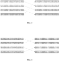
- FIG. 3 and FIG. 4 are schematic diagram of a wire connection manner according to an embodiment of the present disclosure. It can be learned from FIG. 3 that any wire part in the first wire 1 includes a first section of wire part and a second section of wire part. The first section of wire part is a wire part in a left column, and the second section of wire part is a wire part in a right column. It should be noted that the first section of wire part and the second section of wire part are wire parts located in the same layer.
- the first section of wire part and the second section of wire part each include four strands of sub-wires, and a first strand of sub-wire, a second strand of sub-wire, a third strand of sub-wire, and a fourth strand of sub-wire of the first section of wire part are respectively connected to a second strand of sub-wire, a third strand of sub-wire, a fourth strand of sub-wire, and a first strand of sub-wire of the second section of wire part.
- connection manner in FIG. 4 a first strand of sub-wire and a second strand of sub-wire of the first section of wire part are respectively connected to a second strand of sub-wire and a first strand of sub-wire of the second section of wire part, and a third strand of sub-wire and a fourth strand of sub-wire of the first section of wire part are respectively connected to a fourth strand of sub-wire, and a third strand of sub-wire of the second section of wire part.
- the foregoing first section of wire part and second section of wire part each include at least two strands of sub-wires, and an a-th strand of sub-wire of the first section of wire part and a b-th strand of sub-wire of the second section of wire part are connected to each other, so that a skin effect of the first wire 1 is reduced. Therefore, a total current density in the first wire 1 may be evenly distributed as far as possible, an AC effective impedance of the wireless charging coil may be further reduced, and charging efficiency may be improved.
- any wire part in the second wire includes a third section of wire part and a fourth section of wire part
- the third section of wire part and the fourth section of wire part each include at least two strands of sub-wires, a c-th strand of sub-wire of the third section of wire part and a d-th strand of sub-wire of the fourth section of wire part are connected to each other, c and d are both positive integers, and c is not equal to d.
- any wire part in the first wire includes a first section of wire part and a second section of wire part. Principles are the same, and details are not described herein again. It should be noted that the third section of wire part and the fourth section of wire part are wire parts located in the same layer.
- the foregoing third section of wire part and fourth section of wire part each include at least two strands of sub-wires, and a c-th strand of sub-wire of the third section of wire part and a d-th strand of sub-wire of the fourth section of wire part are connected to each other, so that a skin effect of the second wire 2 is reduced. Therefore, a total current density in the second wire 2 may be evenly distributed as far as possible, an AC effective impedance of the wireless charging coil may be further reduced, and charging efficiency may be improved.
- a multi-layer circuit board and the like may also be disposed. This is not limited in this embodiment.
- a wireless charging coil in an embodiment of the present disclosure includes: a first wire 1 and a second wire 2, where the first wire 1 and the second wire 2 are both spirally wound into coils; the first wire 1 includes a first wire part 11 and a second wire part 12 that are connected to each other, and the second wire 2 includes a third wire part 21 and a fourth wire part 22 that are connected to each other; the first wire part 11 is located in a first layer, the second wire part 12 is located in a second layer, the third wire part 21 is located in the first layer, and the fourth wire part 22 is located in the second layer; and the first layer and the second layer are two adjacent layers.
- the first wire 1 and the second wire 2 both have parts in the first layer and the second layer, so that total current densities of the wires are evenly distributed, an AC effective impedance of the wireless charging coil is reduced, and charging efficiency is improved.
- An embodiment of the present disclosure further provides a mobile terminal device, including the foregoing wireless charging coil.
Landscapes
- Engineering & Computer Science (AREA)
- Power Engineering (AREA)
- Computer Networks & Wireless Communication (AREA)
- Charge And Discharge Circuits For Batteries Or The Like (AREA)
- Coils Of Transformers For General Uses (AREA)
Abstract
Description
- This application claims priority to
Chinese Patent Application No.201811146486.4 - The present disclosure relates to the field of wireless charging technologies, and in particular, to a wireless charging coil and a terminal device.
- As wireless charging technologies are developed rapidly, wireless charging is applied to a terminal device more and more widely. Compared with wired charging, the wireless charging has better security and convenience, and an electronic device having a wireless charging function is very popular among users.
- However, during wireless charging, due to a skin effect and a proximity effect, when a current flows through a wireless charging coil, a current density is distributed unevenly, and an effective area of the wireless charging coil through which the current flows is reduced, so that an AC effective impedance of the wireless charging coil through which the current flows is increased, and charging efficiency is relatively low.
- Embodiments of the present disclosure provide a wireless charging coil and a terminal device, to resolve the following problem: When a current flows through the wireless charging coil, a current density is distributed unevenly, and an effective area of the wireless charging coil through which the current flows is reduced, so that an AC effective impedance of the wireless charging coil through which the current flows is increased, and charging efficiency is relatively low.
- To resolve the foregoing technical problem, the present disclosure is implemented as follows:
- According to a first aspect, an embodiment of the present disclosure provides a wireless charging coil, including: a first wire and a second wire, where the first wire and the second wire are both spirally wound into coils, where
the first wire includes a first wire part and a second wire part that are connected to each other, and the second wire includes a third wire part and a fourth wire part that are connected to each other;
the first wire part is located in a first layer, the second wire part is located in a second layer, the third wire part is located in the first layer, and the fourth wire part is located in the second layer; and
the first layer and the second layer are two adjacent layers. - According to a second aspect, an embodiment of the present disclosure further provides a terminal device, including the foregoing wireless charging coil.
- A wireless charging coil in an embodiment of the present disclosure includes: a first wire and a second wire, where the first wire and the second wire are both spirally wound into coils; the first wire includes a first wire part and a second wire part that are connected to each other, and the second wire includes a third wire part and a fourth wire part that are connected to each other; the first wire part is located in a first layer, the second wire part is located in a second layer, the third wire part is located in the first layer, and the fourth wire part is located in the second layer; and the first layer and the second layer are two adjacent layers. In this way, the first wire and the second wire both have parts in the first layer and the second layer, so that total current densities of the wires are evenly distributed, an AC effective impedance of the wireless charging coil is reduced, and charging efficiency is improved.
- To describe the technical solutions in the embodiments of the present disclosure more clearly, the following briefly describes the accompanying drawings required in the embodiments of the present disclosure. Apparently, the accompanying drawings in the following descriptions show merely some embodiments of the present disclosure, and a person of ordinary skill in the art may still derive other drawings from these accompanying drawings without creative efforts.
-
FIG. 1 is a schematic structural diagram of a wireless charging coil according to an embodiment of the present disclosure; -
FIG. 2 is a schematic diagram of current densities of wires according to an embodiment of the present disclosure; -
FIG. 3 is a first schematic diagram of a wire connection manner according to an embodiment of the present disclosure; and -
FIG. 4 is a second schematic diagram of a wire connection manner according to an embodiment of the present disclosure. - The following clearly and completely describes the technical solutions in the embodiments of the present disclosure with reference to the accompanying drawings in the embodiments of the present disclosure. Apparently, the described embodiments are some but not all of the embodiments of the present disclosure. All other embodiments obtained by a person of ordinary skill in the art based on the embodiments of the present disclosure without creative efforts shall fall within the protection scope of the present disclosure.
- Referring to
FIG. 1, FIG. 1 is a schematic structural diagram of a wireless charging coil according to an embodiment of the present disclosure. As shown inFIG. 1 , the wireless charging coil includes: afirst wire 1 and asecond wire 2, where thefirst wire 1 and thesecond wire 2 are both spirally wound into coils; thefirst wire 1 includes afirst wire part 11 and asecond wire part 12 that are connected to each other, and thesecond wire 2 includes athird wire part 21 and afourth wire part 22 that are connected to each other; thefirst wire part 11 is located in a first layer, thesecond wire part 12 is located in a second layer, thethird wire part 21 is located in the first layer, and thefourth wire part 22 is located in the second layer; and the first layer and the second layer are two adjacent layers. - In this embodiment, to better understand the foregoing setting method, in
FIG. 1 , thefirst wire 1 and thesecond wire 2 are described as straight wires, but their principles are the same as that of a wire that is spirally wound into a coil. As shown inFIG. 1 , thefirst wire part 11 of thefirst wire 1 is located in the first layer, and thesecond wire part 12 of thefirst wire 1 is located in the second layer. Because thefirst wire part 11 of the first layer and thefourth wire part 22 of the second layer may have a proximity effect, a current density on an upper side of thefirst wire part 11 may be increased, and a current density on a lower side of thefirst wire part 11 may be decreased (a darker color indicates a larger current density, and a lighter color indicates a smaller current density). - Because the
second wire part 12 of the second layer and thethird wire part 21 of the first layer may also have a proximity effect, a current density on an upper side of thesecond wire part 12 may be decreased, and a current density on a lower side of thesecond wire part 12 may be increased. In this way, the current density on the upper side of thefirst wire part 11 of thefirst wire 1 is large, and the current density on the lower side of thefirst wire part 11 of thefirst wire 1 is small; and the current density on the upper side of thesecond wire part 12 is small, and the current density on the lower side of thesecond wire part 12 is large. Therefore, a total current density in thefirst wire 1 is evenly distributed as far as possible, an AC effective impedance of the wireless charging coil is reduced, and charging efficiency is improved. - Likewise, the current density on the upper side of the
third wire part 21 of thesecond wire 2 is large, and the current density on the lower side of thethird wire part 21 of thesecond wire 2 is small; and the current density on the upper side of thefourth wire part 22 is small, and the current density on the lower side of thefourth wire part 22 is large. Therefore, a total current density in thesecond wire 2 is evenly distributed as far as possible, an AC effective impedance of the wireless charging coil is reduced, and charging efficiency is improved. - In this embodiment, the
first wire part 11 and thesecond wire part 12 of thefirst wire 1 may be connected through a via hole, and thethird wire part 21 and thefourth wire part 22 of thesecond wire 2 may also be connected through a via hole. - To better understand the total current densities of the
first wire 1 and thesecond wire 2, refer toFIG. 2. FIG. 2 is a schematic diagram of current densities of wires according to an embodiment of the present disclosure. It can be learned fromFIG. 2 that after thefirst wire 1 and thesecond wire 2 are arranged in this manner, the total current density of thefirst wire 1 is equivalent to being evenly distributed, and the total current density of thesecond wire 2 is equivalent to being evenly distributed. - In this embodiment, the foregoing terminal device may be a mobile phone, a tablet computer, a laptop computer, a personal digital assistant (personal digital assistant, PDA), a mobile Internet device (Mobile Internet Device, MID), a wearable device, or the like.
- Optionally, the
first wire 1 includes M turns of coils, thesecond wire 2 includes M turns of coils, and M is an integer greater than zero. - In this embodiment, the foregoing
first wire 1 andsecond wire 2 each include M turns of coils, so that thefirst wire 1 may well match thesecond wire 2 in an "interleaving" manner. In addition, the M turns of coils may be a plurality of turns of coils, which may improve wireless charging efficiency. It should be noted that a value of M may be determined based on actual requirements. This is not limited in this embodiment. - Optionally, each turn of coil in the
first wire 1 includes a first coil part and a second coil part, and each turn of coil in thesecond wire 2 includes a third coil part and a fourth coil part; and
the first coil part is included in thefirst wire part 11, the second coil part is included in thesecond wire part 12, the third coil part is included in thethird wire part 21, and the fourth coil part is included in thefourth wire part 22. - In this embodiment, each turn of coil in the foregoing
first wire 1 includes the first coil part and the second coil part. The first coil part is included in thefirst wire part 11, that is, the first coil part is located in the first layer; and the second coil part is included in thesecond wire part 12, that is, the second coil part is located in the second layer. In this way, each turn of coil in thefirst wire 1 has a part that is located in the first layer and a part that is located in the second layer. Therefore, a total current density of each turn of coil may be evenly distributed as far as possible, an AC effective impedance of the wireless charging coil may be further reduced, and charging efficiency may be improved. - Likewise, each turn of coil in the
second wire 2 has a part that is located in the first layer and a part that is located in the second layer. Therefore, a total current density of each turn of coil may be evenly distributed as far as possible, an AC effective impedance of the wireless charging coil may be further reduced, and charging efficiency may be improved. - Optionally, a length of the
first wire part 11 is the same as a length of thesecond wire part 12; and a length of thethird wire part 21 is the same as a length of thefourth wire part 22. - In this embodiment, the length of the foregoing
first wire part 11 is the same as the length of thesecond wire part 12. Therefore, a total current density in thefirst wire 1 may be evenly distributed as far as possible, an AC effective impedance of the wireless charging coil may be further reduced, and charging efficiency may be improved. - In this embodiment, the length of the foregoing
third wire part 21 is the same as the length of thefourth wire part 22. Therefore, a total current density in thesecond wire 2 is evenly distributed as far as possible, an AC effective impedance of the wireless charging coil is further reduced, and charging efficiency is improved. - Optionally, the
first wire 1 includes at least twofirst wire parts 11 and at least twosecond wire parts 12, and any two adjacent wire parts of thefirst wire 1 are different wire parts. - In this embodiment, the foregoing
first wire 1 includes at least twofirst wire parts 11 and at least twosecond wire parts 12, and any two adjacent wire parts of thefirst wire 1 are different wire parts. In this way, the at least twofirst wire parts 11 are located in the first layer, the at least twosecond wire parts 12 are located in the second layer, and any two adjacent wire parts are different wire parts. Therefore, a total current density in thefirst wire 1 may be evenly distributed as far as possible, an AC effective impedance of the wireless charging coil may be further reduced, and charging efficiency may be improved. - Optionally, the
second wire 2 includes at least twothird wire parts 21 and at least twofourth wire parts 22, and any two adjacent wire parts of thesecond wire 2 are different wire parts. - In this embodiment, the foregoing
second wire 2 includes at least twothird wire parts 21 and at least twofourth wire parts 22, and any two adjacent wire parts of thesecond wire 2 are different wire parts. In this way, the at least twothird wire parts 21 are located in the first layer, the at least twofourth wire parts 22 are located in the second layer, and any two adjacent wire parts are different wire parts. Therefore, a total current density in thesecond wire 2 is evenly distributed as far as possible, an AC effective impedance of the wireless charging coil is further reduced, and charging efficiency is improved. - Optionally, any wire part in the
first wire 1 includes a first section of wire part and a second section of wire part, the first section of wire part and the second section of wire part each include at least two strands of sub-wires, an a-th strand of sub-wire of the first section of wire part and a b-th strand of sub-wire of the second section of wire part are connected to each other, a and b are both positive integers, and a is not equal to b. - In this embodiment, to better understand the foregoing setting method, refer to
FIG. 3 and FIG. 4 . Each ofFIG. 3 and FIG. 4 is a schematic diagram of a wire connection manner according to an embodiment of the present disclosure. It can be learned fromFIG. 3 that any wire part in thefirst wire 1 includes a first section of wire part and a second section of wire part. The first section of wire part is a wire part in a left column, and the second section of wire part is a wire part in a right column. It should be noted that the first section of wire part and the second section of wire part are wire parts located in the same layer. - The first section of wire part and the second section of wire part each include four strands of sub-wires, and a first strand of sub-wire, a second strand of sub-wire, a third strand of sub-wire, and a fourth strand of sub-wire of the first section of wire part are respectively connected to a second strand of sub-wire, a third strand of sub-wire, a fourth strand of sub-wire, and a first strand of sub-wire of the second section of wire part.
- Certainly, in addition to this connection manner, reference may also be made to the connection manner in
FIG. 4 . InFIG. 4 , a first strand of sub-wire and a second strand of sub-wire of the first section of wire part are respectively connected to a second strand of sub-wire and a first strand of sub-wire of the second section of wire part, and a third strand of sub-wire and a fourth strand of sub-wire of the first section of wire part are respectively connected to a fourth strand of sub-wire, and a third strand of sub-wire of the second section of wire part. - In this embodiment, the foregoing first section of wire part and second section of wire part each include at least two strands of sub-wires, and an a-th strand of sub-wire of the first section of wire part and a b-th strand of sub-wire of the second section of wire part are connected to each other, so that a skin effect of the
first wire 1 is reduced. Therefore, a total current density in thefirst wire 1 may be evenly distributed as far as possible, an AC effective impedance of the wireless charging coil may be further reduced, and charging efficiency may be improved. - Optionally, any wire part in the second wire includes a third section of wire part and a fourth section of wire part, the third section of wire part and the fourth section of wire part each include at least two strands of sub-wires, a c-th strand of sub-wire of the third section of wire part and a d-th strand of sub-wire of the fourth section of wire part are connected to each other, c and d are both positive integers, and c is not equal to d.
- In this embodiment, for understanding, reference may be made to that any wire part in the first wire includes a first section of wire part and a second section of wire part. Principles are the same, and details are not described herein again. It should be noted that the third section of wire part and the fourth section of wire part are wire parts located in the same layer.
- In this embodiment, the foregoing third section of wire part and fourth section of wire part each include at least two strands of sub-wires, and a c-th strand of sub-wire of the third section of wire part and a d-th strand of sub-wire of the fourth section of wire part are connected to each other, so that a skin effect of the
second wire 2 is reduced. Therefore, a total current density in thesecond wire 2 may be evenly distributed as far as possible, an AC effective impedance of the wireless charging coil may be further reduced, and charging efficiency may be improved. Certainly, in addition to this, a multi-layer circuit board and the like may also be disposed. This is not limited in this embodiment. - A wireless charging coil in an embodiment of the present disclosure includes: a
first wire 1 and asecond wire 2, where thefirst wire 1 and thesecond wire 2 are both spirally wound into coils; thefirst wire 1 includes afirst wire part 11 and asecond wire part 12 that are connected to each other, and thesecond wire 2 includes athird wire part 21 and afourth wire part 22 that are connected to each other; thefirst wire part 11 is located in a first layer, thesecond wire part 12 is located in a second layer, thethird wire part 21 is located in the first layer, and thefourth wire part 22 is located in the second layer; and the first layer and the second layer are two adjacent layers. In this way, thefirst wire 1 and thesecond wire 2 both have parts in the first layer and the second layer, so that total current densities of the wires are evenly distributed, an AC effective impedance of the wireless charging coil is reduced, and charging efficiency is improved. - An embodiment of the present disclosure further provides a mobile terminal device, including the foregoing wireless charging coil.
- It should be noted that in this specification, the terms "comprise", "include" and any other variants thereof are intended to cover non-exclusive inclusion, so that a process, a method, an article, or an apparatus that includes a series of elements not only includes these very elements, but may also include other elements not expressly listed, or also include elements inherent to this process, method, article, or apparatus. Without being subject to further limitations, an element defined by a phrase "including a ......" does not exclude presence of other identical elements in the process, method, article, or apparatus that includes the very element.
- The embodiments of the present disclosure are described above with reference to the accompanying drawings, but the present disclosure is not limited to the foregoing specific implementations. The foregoing specific implementations are merely schematic instead of restrictive. Under enlightenment of the present disclosure, a person of ordinary skills in the art may make many forms without departing from the protection scope of aims of the present disclosure and claims, all of which fall within the protection of the present disclosure.
Claims (9)
- A wireless charging coil, comprising: a first wire and a second wire, wherein the first wire and the second wire are both spirally wound into coils;
the first wire comprises a first wire part and a second wire part that are connected to each other, and the second wire comprises a third wire part and a fourth wire part that are connected to each other;
the first wire part is located in a first layer, the second wire part is located in a second layer, the third wire part is located in the first layer, and the fourth wire part is located in the second layer; and
the first layer and the second layer are two adjacent layers. - The wireless charging coil according to claim 1, wherein the first wire comprises M turns of coils, the second wire comprises M turns of coils, and M is an integer greater than zero.
- The wireless charging coil according to claim 2, wherein each turn of coil in the first wire comprises a first coil part and a second coil part, and each turn of coil in the second wire comprises a third coil part and a fourth coil part; and
the first coil part is comprised in the first wire part, the second coil part is comprised in the second wire part, the third coil part is comprised in the third wire part, and the fourth coil part is comprised in the fourth wire part. - The wireless charging coil according to claim 1, wherein a length of the first wire part is the same as a length of the second wire part; and a length of the third wire part is the same as a length of the fourth wire part.
- The wireless charging coil according to claim 1, wherein the first wire comprises at least two first wire parts and at least two second wire parts, and any two adjacent wire parts of the first wire are different wire parts.
- The wireless charging coil according to claim 1, wherein the second wire comprises at least two third wire parts and at least two fourth wire parts, and any two adjacent wire parts of the second wire are different wire parts.
- The wireless charging coil according to claim 1, wherein any wire part in the first wire comprises a first section of wire part and a second section of wire part, the first section of wire part and the second section of wire part each comprise at least two strands of sub-wires, an a-th strand of sub-wire of the first section of wire part and a b-th strand of sub-wire of the second section of wire part are connected to each other, a and b are both positive integers, and a is not equal to b.
- The wireless charging coil according to claim 1, wherein any wire part in the second wire comprises a third section of wire part and a fourth section of wire part, the third section of wire part and the fourth section of wire part each comprise at least two strands of sub-wires, a c-th strand of sub-wire of the third section of wire part and a d-th strand of sub-wire of the fourth section of wire part are connected to each other, c and d are both positive integers, and c is not equal to d.
- A terminal device, comprising the wireless charging coil according to any one of claims 1 to 8.
Applications Claiming Priority (2)
| Application Number | Priority Date | Filing Date | Title |
|---|---|---|---|
| CN201811146486.4A CN109215978B (en) | 2018-09-29 | 2018-09-29 | Wireless charging coil and terminal equipment |
| PCT/CN2019/107754 WO2020063644A1 (en) | 2018-09-29 | 2019-09-25 | Wireless charging coil and terminal device |
Publications (3)
| Publication Number | Publication Date |
|---|---|
| EP3859759A1 true EP3859759A1 (en) | 2021-08-04 |
| EP3859759A4 EP3859759A4 (en) | 2022-01-26 |
| EP3859759B1 EP3859759B1 (en) | 2023-11-08 |
Family
ID=64982407
Family Applications (1)
| Application Number | Title | Priority Date | Filing Date |
|---|---|---|---|
| EP19865562.3A Active EP3859759B1 (en) | 2018-09-29 | 2019-09-25 | Wireless charging coil and terminal device |
Country Status (5)
| Country | Link |
|---|---|
| US (1) | US11875932B2 (en) |
| EP (1) | EP3859759B1 (en) |
| CN (1) | CN109215978B (en) |
| ES (1) | ES2966407T3 (en) |
| WO (1) | WO2020063644A1 (en) |
Families Citing this family (9)
| Publication number | Priority date | Publication date | Assignee | Title |
|---|---|---|---|---|
| CN110958662B (en) | 2018-09-27 | 2022-11-22 | 维沃移动通信有限公司 | Access control method, terminal and network side device |
| CN109066055B (en) | 2018-09-28 | 2020-10-20 | 维沃移动通信有限公司 | a terminal device |
| CN110971357B (en) | 2018-09-28 | 2021-04-27 | 维沃移动通信有限公司 | Information indication method, indication receiving method, terminal and network side device |
| CN109215978B (en) * | 2018-09-29 | 2021-01-08 | 维沃移动通信有限公司 | Wireless charging coil and terminal equipment |
| CN110971641B (en) | 2018-09-30 | 2022-04-19 | 维沃移动通信有限公司 | Network service control method and communication equipment |
| CN111030789B (en) | 2018-10-10 | 2021-04-23 | 维沃移动通信有限公司 | Processing method and terminal |
| CN109167420B (en) | 2018-10-31 | 2020-11-03 | 维沃移动通信有限公司 | A charging control circuit, charging circuit and charging control method |
| CN111132203B (en) | 2018-10-31 | 2021-11-16 | 维沃移动通信有限公司 | Processing method and terminal |
| CN115249559A (en) * | 2021-04-27 | 2022-10-28 | 北京小米移动软件有限公司 | Wireless charging coil, electronic equipment and winding method of wireless charging coil |
Family Cites Families (11)
| Publication number | Priority date | Publication date | Assignee | Title |
|---|---|---|---|---|
| US5430247A (en) * | 1993-08-31 | 1995-07-04 | Motorola, Inc. | Twisted-pair planar conductor line off-set structure |
| KR100349419B1 (en) * | 1999-07-27 | 2002-08-19 | 학교법인 한국정보통신학원 | Dual-layer spiral inductor |
| US7973635B2 (en) * | 2007-09-28 | 2011-07-05 | Access Business Group International Llc | Printed circuit board coil |
| CN101409429B (en) * | 2008-12-04 | 2011-03-23 | 天水长城开关厂有限公司 | Method for improving multi-slice rectangle conductor current-carrying capacity and large current-carrying rectangle conductor |
| CN203826973U (en) * | 2013-10-14 | 2014-09-10 | 山东三泰节能技术服务有限公司 | Electromagnetic-balance filtering power-saving device |
| DE102014220978A1 (en) * | 2014-10-16 | 2016-04-21 | Robert Bosch Gmbh | Coil arrangement for inductive energy transmission, inductive energy transmission device and method for producing a coil arrangement for inductive energy transmission |
| CN206023383U (en) * | 2016-09-13 | 2017-03-15 | 苏州纳格光电科技有限公司 | wireless charging receiving coil |
| CN106849554B (en) * | 2017-01-23 | 2023-07-14 | 河北新四达电机股份有限公司 | Permanent magnet motor stator and multi-parallel winding soft winding transposition coil inserting method thereof |
| CN108565102B (en) | 2018-03-28 | 2020-08-14 | 华为技术有限公司 | Coil module, wireless charging transmitting device, wireless charging receiving device, wireless charging system and wireless charging terminal |
| CN109215978B (en) * | 2018-09-29 | 2021-01-08 | 维沃移动通信有限公司 | Wireless charging coil and terminal equipment |
| CN110289156B (en) * | 2019-05-24 | 2020-11-10 | 华为技术有限公司 | Coil winding, coil module, transmitting device, receiving device, system and terminal |
-
2018
- 2018-09-29 CN CN201811146486.4A patent/CN109215978B/en active Active
-
2019
- 2019-09-25 EP EP19865562.3A patent/EP3859759B1/en active Active
- 2019-09-25 ES ES19865562T patent/ES2966407T3/en active Active
- 2019-09-25 WO PCT/CN2019/107754 patent/WO2020063644A1/en not_active Ceased
-
2021
- 2021-03-25 US US17/211,913 patent/US11875932B2/en active Active
Also Published As
| Publication number | Publication date |
|---|---|
| EP3859759B1 (en) | 2023-11-08 |
| US20210210283A1 (en) | 2021-07-08 |
| US11875932B2 (en) | 2024-01-16 |
| ES2966407T3 (en) | 2024-04-22 |
| CN109215978B (en) | 2021-01-08 |
| EP3859759A4 (en) | 2022-01-26 |
| WO2020063644A1 (en) | 2020-04-02 |
| CN109215978A (en) | 2019-01-15 |
Similar Documents
| Publication | Publication Date | Title |
|---|---|---|
| US11875932B2 (en) | Wireless charging coil and terminal device | |
| CN104347262B (en) | Method for manufacturing multilayer coil | |
| JP6548198B2 (en) | Chip electronic components | |
| US7889047B2 (en) | Magnetic device | |
| JP6366933B2 (en) | Common mode filter and manufacturing method thereof | |
| CN109087791A (en) | Coil component | |
| JP2015092499A5 (en) | ||
| US10586647B2 (en) | Electronic component | |
| US7167070B2 (en) | Laminated coil component and method of producing the same | |
| US20100193506A1 (en) | Litz wire coil | |
| CN109585136A (en) | Multilayer coil component | |
| US10847305B2 (en) | Coil component | |
| CN101587769A (en) | Magnetic element | |
| US20210383947A1 (en) | Winding wire having insulation layer wrapping around multiple wires | |
| JPWO2014185468A1 (en) | Signal cable and wire harness | |
| WO2023103317A1 (en) | Electronic element and high-frequency winding thereof | |
| CN108110917B (en) | stator | |
| CN101471173B (en) | Combined inductor | |
| JP6044214B2 (en) | Litz wire and high frequency power supply coil | |
| CN111180173A (en) | A wireless charging coil and wireless charging device | |
| CN205723118U (en) | A kind of multi-groove type rectifier transformer | |
| CN206312617U (en) | A kind of transformer winding cable | |
| CN202771816U (en) | Signal line structure | |
| CN220569520U (en) | Coil modules, wireless charging devices and smart terminals | |
| CN209657972U (en) | A wireless charging coil, wireless charging device and terminal equipment |
Legal Events
| Date | Code | Title | Description |
|---|---|---|---|
| STAA | Information on the status of an ep patent application or granted ep patent |
Free format text: STATUS: THE INTERNATIONAL PUBLICATION HAS BEEN MADE |
|
| PUAI | Public reference made under article 153(3) epc to a published international application that has entered the european phase |
Free format text: ORIGINAL CODE: 0009012 |
|
| STAA | Information on the status of an ep patent application or granted ep patent |
Free format text: STATUS: REQUEST FOR EXAMINATION WAS MADE |
|
| 17P | Request for examination filed |
Effective date: 20210415 |
|
| AK | Designated contracting states |
Kind code of ref document: A1 Designated state(s): AL AT BE BG CH CY CZ DE DK EE ES FI FR GB GR HR HU IE IS IT LI LT LU LV MC MK MT NL NO PL PT RO RS SE SI SK SM TR |
|
| DAV | Request for validation of the european patent (deleted) | ||
| DAX | Request for extension of the european patent (deleted) | ||
| A4 | Supplementary search report drawn up and despatched |
Effective date: 20220107 |
|
| RIC1 | Information provided on ipc code assigned before grant |
Ipc: H02J 50/00 20160101ALI20211223BHEP Ipc: H01F 38/14 20060101ALI20211223BHEP Ipc: H01F 27/34 20060101ALI20211223BHEP Ipc: H02J 50/10 20160101ALI20211223BHEP Ipc: H01F 27/28 20060101AFI20211223BHEP |
|
| GRAP | Despatch of communication of intention to grant a patent |
Free format text: ORIGINAL CODE: EPIDOSNIGR1 |
|
| STAA | Information on the status of an ep patent application or granted ep patent |
Free format text: STATUS: GRANT OF PATENT IS INTENDED |
|
| INTG | Intention to grant announced |
Effective date: 20230829 |
|
| GRAS | Grant fee paid |
Free format text: ORIGINAL CODE: EPIDOSNIGR3 |
|
| GRAA | (expected) grant |
Free format text: ORIGINAL CODE: 0009210 |
|
| STAA | Information on the status of an ep patent application or granted ep patent |
Free format text: STATUS: THE PATENT HAS BEEN GRANTED |
|
| AK | Designated contracting states |
Kind code of ref document: B1 Designated state(s): AL AT BE BG CH CY CZ DE DK EE ES FI FR GB GR HR HU IE IS IT LI LT LU LV MC MK MT NL NO PL PT RO RS SE SI SK SM TR |
|
| REG | Reference to a national code |
Ref country code: GB Ref legal event code: FG4D |
|
| REG | Reference to a national code |
Ref country code: CH Ref legal event code: EP |
|
| REG | Reference to a national code |
Ref country code: DE Ref legal event code: R096 Ref document number: 602019041237 Country of ref document: DE |
|
| REG | Reference to a national code |
Ref country code: IE Ref legal event code: FG4D |
|
| REG | Reference to a national code |
Ref country code: NL Ref legal event code: FP |
|
| REG | Reference to a national code |
Ref country code: LT Ref legal event code: MG9D |
|
| PG25 | Lapsed in a contracting state [announced via postgrant information from national office to epo] |
Ref country code: GR Free format text: LAPSE BECAUSE OF FAILURE TO SUBMIT A TRANSLATION OF THE DESCRIPTION OR TO PAY THE FEE WITHIN THE PRESCRIBED TIME-LIMIT Effective date: 20240209 |
|
| PG25 | Lapsed in a contracting state [announced via postgrant information from national office to epo] |
Ref country code: IS Free format text: LAPSE BECAUSE OF FAILURE TO SUBMIT A TRANSLATION OF THE DESCRIPTION OR TO PAY THE FEE WITHIN THE PRESCRIBED TIME-LIMIT Effective date: 20240308 |
|
| PG25 | Lapsed in a contracting state [announced via postgrant information from national office to epo] |
Ref country code: LT Free format text: LAPSE BECAUSE OF FAILURE TO SUBMIT A TRANSLATION OF THE DESCRIPTION OR TO PAY THE FEE WITHIN THE PRESCRIBED TIME-LIMIT Effective date: 20231108 |
|
| REG | Reference to a national code |
Ref country code: AT Ref legal event code: MK05 Ref document number: 1630425 Country of ref document: AT Kind code of ref document: T Effective date: 20231108 |
|
| REG | Reference to a national code |
Ref country code: ES Ref legal event code: FG2A Ref document number: 2966407 Country of ref document: ES Kind code of ref document: T3 Effective date: 20240422 |
|
| PG25 | Lapsed in a contracting state [announced via postgrant information from national office to epo] |
Ref country code: AT Free format text: LAPSE BECAUSE OF FAILURE TO SUBMIT A TRANSLATION OF THE DESCRIPTION OR TO PAY THE FEE WITHIN THE PRESCRIBED TIME-LIMIT Effective date: 20231108 |
|
| PG25 | Lapsed in a contracting state [announced via postgrant information from national office to epo] |
Ref country code: LT Free format text: LAPSE BECAUSE OF FAILURE TO SUBMIT A TRANSLATION OF THE DESCRIPTION OR TO PAY THE FEE WITHIN THE PRESCRIBED TIME-LIMIT Effective date: 20231108 Ref country code: IS Free format text: LAPSE BECAUSE OF FAILURE TO SUBMIT A TRANSLATION OF THE DESCRIPTION OR TO PAY THE FEE WITHIN THE PRESCRIBED TIME-LIMIT Effective date: 20240308 Ref country code: GR Free format text: LAPSE BECAUSE OF FAILURE TO SUBMIT A TRANSLATION OF THE DESCRIPTION OR TO PAY THE FEE WITHIN THE PRESCRIBED TIME-LIMIT Effective date: 20240209 Ref country code: BG Free format text: LAPSE BECAUSE OF FAILURE TO SUBMIT A TRANSLATION OF THE DESCRIPTION OR TO PAY THE FEE WITHIN THE PRESCRIBED TIME-LIMIT Effective date: 20240208 Ref country code: AT Free format text: LAPSE BECAUSE OF FAILURE TO SUBMIT A TRANSLATION OF THE DESCRIPTION OR TO PAY THE FEE WITHIN THE PRESCRIBED TIME-LIMIT Effective date: 20231108 Ref country code: PT Free format text: LAPSE BECAUSE OF FAILURE TO SUBMIT A TRANSLATION OF THE DESCRIPTION OR TO PAY THE FEE WITHIN THE PRESCRIBED TIME-LIMIT Effective date: 20240308 |
|
| PG25 | Lapsed in a contracting state [announced via postgrant information from national office to epo] |
Ref country code: SE Free format text: LAPSE BECAUSE OF FAILURE TO SUBMIT A TRANSLATION OF THE DESCRIPTION OR TO PAY THE FEE WITHIN THE PRESCRIBED TIME-LIMIT Effective date: 20231108 Ref country code: RS Free format text: LAPSE BECAUSE OF FAILURE TO SUBMIT A TRANSLATION OF THE DESCRIPTION OR TO PAY THE FEE WITHIN THE PRESCRIBED TIME-LIMIT Effective date: 20231108 Ref country code: PL Free format text: LAPSE BECAUSE OF FAILURE TO SUBMIT A TRANSLATION OF THE DESCRIPTION OR TO PAY THE FEE WITHIN THE PRESCRIBED TIME-LIMIT Effective date: 20231108 Ref country code: NO Free format text: LAPSE BECAUSE OF FAILURE TO SUBMIT A TRANSLATION OF THE DESCRIPTION OR TO PAY THE FEE WITHIN THE PRESCRIBED TIME-LIMIT Effective date: 20240208 Ref country code: LV Free format text: LAPSE BECAUSE OF FAILURE TO SUBMIT A TRANSLATION OF THE DESCRIPTION OR TO PAY THE FEE WITHIN THE PRESCRIBED TIME-LIMIT Effective date: 20231108 Ref country code: HR Free format text: LAPSE BECAUSE OF FAILURE TO SUBMIT A TRANSLATION OF THE DESCRIPTION OR TO PAY THE FEE WITHIN THE PRESCRIBED TIME-LIMIT Effective date: 20231108 |
|
| PG25 | Lapsed in a contracting state [announced via postgrant information from national office to epo] |
Ref country code: DK Free format text: LAPSE BECAUSE OF FAILURE TO SUBMIT A TRANSLATION OF THE DESCRIPTION OR TO PAY THE FEE WITHIN THE PRESCRIBED TIME-LIMIT Effective date: 20231108 |
|
| PG25 | Lapsed in a contracting state [announced via postgrant information from national office to epo] |
Ref country code: CZ Free format text: LAPSE BECAUSE OF FAILURE TO SUBMIT A TRANSLATION OF THE DESCRIPTION OR TO PAY THE FEE WITHIN THE PRESCRIBED TIME-LIMIT Effective date: 20231108 |
|
| PG25 | Lapsed in a contracting state [announced via postgrant information from national office to epo] |
Ref country code: SK Free format text: LAPSE BECAUSE OF FAILURE TO SUBMIT A TRANSLATION OF THE DESCRIPTION OR TO PAY THE FEE WITHIN THE PRESCRIBED TIME-LIMIT Effective date: 20231108 |
|
| PG25 | Lapsed in a contracting state [announced via postgrant information from national office to epo] |
Ref country code: SM Free format text: LAPSE BECAUSE OF FAILURE TO SUBMIT A TRANSLATION OF THE DESCRIPTION OR TO PAY THE FEE WITHIN THE PRESCRIBED TIME-LIMIT Effective date: 20231108 Ref country code: SK Free format text: LAPSE BECAUSE OF FAILURE TO SUBMIT A TRANSLATION OF THE DESCRIPTION OR TO PAY THE FEE WITHIN THE PRESCRIBED TIME-LIMIT Effective date: 20231108 Ref country code: RO Free format text: LAPSE BECAUSE OF FAILURE TO SUBMIT A TRANSLATION OF THE DESCRIPTION OR TO PAY THE FEE WITHIN THE PRESCRIBED TIME-LIMIT Effective date: 20231108 Ref country code: EE Free format text: LAPSE BECAUSE OF FAILURE TO SUBMIT A TRANSLATION OF THE DESCRIPTION OR TO PAY THE FEE WITHIN THE PRESCRIBED TIME-LIMIT Effective date: 20231108 Ref country code: DK Free format text: LAPSE BECAUSE OF FAILURE TO SUBMIT A TRANSLATION OF THE DESCRIPTION OR TO PAY THE FEE WITHIN THE PRESCRIBED TIME-LIMIT Effective date: 20231108 Ref country code: CZ Free format text: LAPSE BECAUSE OF FAILURE TO SUBMIT A TRANSLATION OF THE DESCRIPTION OR TO PAY THE FEE WITHIN THE PRESCRIBED TIME-LIMIT Effective date: 20231108 |
|
| REG | Reference to a national code |
Ref country code: DE Ref legal event code: R097 Ref document number: 602019041237 Country of ref document: DE |
|
| PLBE | No opposition filed within time limit |
Free format text: ORIGINAL CODE: 0009261 |
|
| STAA | Information on the status of an ep patent application or granted ep patent |
Free format text: STATUS: NO OPPOSITION FILED WITHIN TIME LIMIT |
|
| 26N | No opposition filed |
Effective date: 20240809 |
|
| PG25 | Lapsed in a contracting state [announced via postgrant information from national office to epo] |
Ref country code: SI Free format text: LAPSE BECAUSE OF FAILURE TO SUBMIT A TRANSLATION OF THE DESCRIPTION OR TO PAY THE FEE WITHIN THE PRESCRIBED TIME-LIMIT Effective date: 20231108 |
|
| PG25 | Lapsed in a contracting state [announced via postgrant information from national office to epo] |
Ref country code: SI Free format text: LAPSE BECAUSE OF FAILURE TO SUBMIT A TRANSLATION OF THE DESCRIPTION OR TO PAY THE FEE WITHIN THE PRESCRIBED TIME-LIMIT Effective date: 20231108 |
|
| PG25 | Lapsed in a contracting state [announced via postgrant information from national office to epo] |
Ref country code: MC Free format text: LAPSE BECAUSE OF FAILURE TO SUBMIT A TRANSLATION OF THE DESCRIPTION OR TO PAY THE FEE WITHIN THE PRESCRIBED TIME-LIMIT Effective date: 20231108 |
|
| REG | Reference to a national code |
Ref country code: CH Ref legal event code: PL |
|
| PG25 | Lapsed in a contracting state [announced via postgrant information from national office to epo] |
Ref country code: LU Free format text: LAPSE BECAUSE OF NON-PAYMENT OF DUE FEES Effective date: 20240925 |
|
| REG | Reference to a national code |
Ref country code: BE Ref legal event code: MM Effective date: 20240930 |
|
| PG25 | Lapsed in a contracting state [announced via postgrant information from national office to epo] |
Ref country code: BE Free format text: LAPSE BECAUSE OF NON-PAYMENT OF DUE FEES Effective date: 20240930 |
|
| PG25 | Lapsed in a contracting state [announced via postgrant information from national office to epo] |
Ref country code: CH Free format text: LAPSE BECAUSE OF NON-PAYMENT OF DUE FEES Effective date: 20240930 |
|
| PG25 | Lapsed in a contracting state [announced via postgrant information from national office to epo] |
Ref country code: IE Free format text: LAPSE BECAUSE OF NON-PAYMENT OF DUE FEES Effective date: 20240925 |
|
| PGFP | Annual fee paid to national office [announced via postgrant information from national office to epo] |
Ref country code: NL Payment date: 20250814 Year of fee payment: 7 |
|
| PG25 | Lapsed in a contracting state [announced via postgrant information from national office to epo] |
Ref country code: FI Free format text: LAPSE BECAUSE OF FAILURE TO SUBMIT A TRANSLATION OF THE DESCRIPTION OR TO PAY THE FEE WITHIN THE PRESCRIBED TIME-LIMIT Effective date: 20231108 |
|
| PGFP | Annual fee paid to national office [announced via postgrant information from national office to epo] |
Ref country code: DE Payment date: 20250730 Year of fee payment: 7 |
|
| PGFP | Annual fee paid to national office [announced via postgrant information from national office to epo] |
Ref country code: IT Payment date: 20250825 Year of fee payment: 7 |
|
| PGFP | Annual fee paid to national office [announced via postgrant information from national office to epo] |
Ref country code: GB Payment date: 20250807 Year of fee payment: 7 |
|
| PGFP | Annual fee paid to national office [announced via postgrant information from national office to epo] |
Ref country code: FR Payment date: 20250808 Year of fee payment: 7 |
|
| PG25 | Lapsed in a contracting state [announced via postgrant information from national office to epo] |
Ref country code: CY Free format text: LAPSE BECAUSE OF FAILURE TO SUBMIT A TRANSLATION OF THE DESCRIPTION OR TO PAY THE FEE WITHIN THE PRESCRIBED TIME-LIMIT; INVALID AB INITIO Effective date: 20190925 |
|
| PGFP | Annual fee paid to national office [announced via postgrant information from national office to epo] |
Ref country code: ES Payment date: 20251014 Year of fee payment: 7 |
|
| PG25 | Lapsed in a contracting state [announced via postgrant information from national office to epo] |
Ref country code: HU Free format text: LAPSE BECAUSE OF FAILURE TO SUBMIT A TRANSLATION OF THE DESCRIPTION OR TO PAY THE FEE WITHIN THE PRESCRIBED TIME-LIMIT; INVALID AB INITIO Effective date: 20190925 |