EP3859725A2 - Display device - Google Patents
Display device Download PDFInfo
- Publication number
- EP3859725A2 EP3859725A2 EP20217822.4A EP20217822A EP3859725A2 EP 3859725 A2 EP3859725 A2 EP 3859725A2 EP 20217822 A EP20217822 A EP 20217822A EP 3859725 A2 EP3859725 A2 EP 3859725A2
- Authority
- EP
- European Patent Office
- Prior art keywords
- area
- resolution
- low
- boundary
- unit pixels
- Prior art date
- Legal status (The legal status is an assumption and is not a legal conclusion. Google has not performed a legal analysis and makes no representation as to the accuracy of the status listed.)
- Pending
Links
Images







Classifications
-
- G—PHYSICS
- G09—EDUCATION; CRYPTOGRAPHY; DISPLAY; ADVERTISING; SEALS
- G09G—ARRANGEMENTS OR CIRCUITS FOR CONTROL OF INDICATING DEVICES USING STATIC MEANS TO PRESENT VARIABLE INFORMATION
- G09G3/00—Control arrangements or circuits, of interest only in connection with visual indicators other than cathode-ray tubes
- G09G3/20—Control arrangements or circuits, of interest only in connection with visual indicators other than cathode-ray tubes for presentation of an assembly of a number of characters, e.g. a page, by composing the assembly by combination of individual elements arranged in a matrix no fixed position being assigned to or needed to be assigned to the individual characters or partial characters
- G09G3/22—Control arrangements or circuits, of interest only in connection with visual indicators other than cathode-ray tubes for presentation of an assembly of a number of characters, e.g. a page, by composing the assembly by combination of individual elements arranged in a matrix no fixed position being assigned to or needed to be assigned to the individual characters or partial characters using controlled light sources
- G09G3/30—Control arrangements or circuits, of interest only in connection with visual indicators other than cathode-ray tubes for presentation of an assembly of a number of characters, e.g. a page, by composing the assembly by combination of individual elements arranged in a matrix no fixed position being assigned to or needed to be assigned to the individual characters or partial characters using controlled light sources using electroluminescent panels
- G09G3/32—Control arrangements or circuits, of interest only in connection with visual indicators other than cathode-ray tubes for presentation of an assembly of a number of characters, e.g. a page, by composing the assembly by combination of individual elements arranged in a matrix no fixed position being assigned to or needed to be assigned to the individual characters or partial characters using controlled light sources using electroluminescent panels semiconductive, e.g. using light-emitting diodes [LED]
- G09G3/3208—Control arrangements or circuits, of interest only in connection with visual indicators other than cathode-ray tubes for presentation of an assembly of a number of characters, e.g. a page, by composing the assembly by combination of individual elements arranged in a matrix no fixed position being assigned to or needed to be assigned to the individual characters or partial characters using controlled light sources using electroluminescent panels semiconductive, e.g. using light-emitting diodes [LED] organic, e.g. using organic light-emitting diodes [OLED]
- G09G3/3225—Control arrangements or circuits, of interest only in connection with visual indicators other than cathode-ray tubes for presentation of an assembly of a number of characters, e.g. a page, by composing the assembly by combination of individual elements arranged in a matrix no fixed position being assigned to or needed to be assigned to the individual characters or partial characters using controlled light sources using electroluminescent panels semiconductive, e.g. using light-emitting diodes [LED] organic, e.g. using organic light-emitting diodes [OLED] using an active matrix
-
- G—PHYSICS
- G09—EDUCATION; CRYPTOGRAPHY; DISPLAY; ADVERTISING; SEALS
- G09G—ARRANGEMENTS OR CIRCUITS FOR CONTROL OF INDICATING DEVICES USING STATIC MEANS TO PRESENT VARIABLE INFORMATION
- G09G3/00—Control arrangements or circuits, of interest only in connection with visual indicators other than cathode-ray tubes
- G09G3/20—Control arrangements or circuits, of interest only in connection with visual indicators other than cathode-ray tubes for presentation of an assembly of a number of characters, e.g. a page, by composing the assembly by combination of individual elements arranged in a matrix no fixed position being assigned to or needed to be assigned to the individual characters or partial characters
- G09G3/2003—Display of colours
-
- G—PHYSICS
- G09—EDUCATION; CRYPTOGRAPHY; DISPLAY; ADVERTISING; SEALS
- G09G—ARRANGEMENTS OR CIRCUITS FOR CONTROL OF INDICATING DEVICES USING STATIC MEANS TO PRESENT VARIABLE INFORMATION
- G09G3/00—Control arrangements or circuits, of interest only in connection with visual indicators other than cathode-ray tubes
- G09G3/20—Control arrangements or circuits, of interest only in connection with visual indicators other than cathode-ray tubes for presentation of an assembly of a number of characters, e.g. a page, by composing the assembly by combination of individual elements arranged in a matrix no fixed position being assigned to or needed to be assigned to the individual characters or partial characters
- G09G3/22—Control arrangements or circuits, of interest only in connection with visual indicators other than cathode-ray tubes for presentation of an assembly of a number of characters, e.g. a page, by composing the assembly by combination of individual elements arranged in a matrix no fixed position being assigned to or needed to be assigned to the individual characters or partial characters using controlled light sources
- G09G3/30—Control arrangements or circuits, of interest only in connection with visual indicators other than cathode-ray tubes for presentation of an assembly of a number of characters, e.g. a page, by composing the assembly by combination of individual elements arranged in a matrix no fixed position being assigned to or needed to be assigned to the individual characters or partial characters using controlled light sources using electroluminescent panels
- G09G3/32—Control arrangements or circuits, of interest only in connection with visual indicators other than cathode-ray tubes for presentation of an assembly of a number of characters, e.g. a page, by composing the assembly by combination of individual elements arranged in a matrix no fixed position being assigned to or needed to be assigned to the individual characters or partial characters using controlled light sources using electroluminescent panels semiconductive, e.g. using light-emitting diodes [LED]
- G09G3/3208—Control arrangements or circuits, of interest only in connection with visual indicators other than cathode-ray tubes for presentation of an assembly of a number of characters, e.g. a page, by composing the assembly by combination of individual elements arranged in a matrix no fixed position being assigned to or needed to be assigned to the individual characters or partial characters using controlled light sources using electroluminescent panels semiconductive, e.g. using light-emitting diodes [LED] organic, e.g. using organic light-emitting diodes [OLED]
- G09G3/3225—Control arrangements or circuits, of interest only in connection with visual indicators other than cathode-ray tubes for presentation of an assembly of a number of characters, e.g. a page, by composing the assembly by combination of individual elements arranged in a matrix no fixed position being assigned to or needed to be assigned to the individual characters or partial characters using controlled light sources using electroluminescent panels semiconductive, e.g. using light-emitting diodes [LED] organic, e.g. using organic light-emitting diodes [OLED] using an active matrix
- G09G3/3233—Control arrangements or circuits, of interest only in connection with visual indicators other than cathode-ray tubes for presentation of an assembly of a number of characters, e.g. a page, by composing the assembly by combination of individual elements arranged in a matrix no fixed position being assigned to or needed to be assigned to the individual characters or partial characters using controlled light sources using electroluminescent panels semiconductive, e.g. using light-emitting diodes [LED] organic, e.g. using organic light-emitting diodes [OLED] using an active matrix with pixel circuitry controlling the current through the light-emitting element
-
- G—PHYSICS
- G09—EDUCATION; CRYPTOGRAPHY; DISPLAY; ADVERTISING; SEALS
- G09G—ARRANGEMENTS OR CIRCUITS FOR CONTROL OF INDICATING DEVICES USING STATIC MEANS TO PRESENT VARIABLE INFORMATION
- G09G3/00—Control arrangements or circuits, of interest only in connection with visual indicators other than cathode-ray tubes
- G09G3/20—Control arrangements or circuits, of interest only in connection with visual indicators other than cathode-ray tubes for presentation of an assembly of a number of characters, e.g. a page, by composing the assembly by combination of individual elements arranged in a matrix no fixed position being assigned to or needed to be assigned to the individual characters or partial characters
- G09G3/22—Control arrangements or circuits, of interest only in connection with visual indicators other than cathode-ray tubes for presentation of an assembly of a number of characters, e.g. a page, by composing the assembly by combination of individual elements arranged in a matrix no fixed position being assigned to or needed to be assigned to the individual characters or partial characters using controlled light sources
- G09G3/30—Control arrangements or circuits, of interest only in connection with visual indicators other than cathode-ray tubes for presentation of an assembly of a number of characters, e.g. a page, by composing the assembly by combination of individual elements arranged in a matrix no fixed position being assigned to or needed to be assigned to the individual characters or partial characters using controlled light sources using electroluminescent panels
- G09G3/32—Control arrangements or circuits, of interest only in connection with visual indicators other than cathode-ray tubes for presentation of an assembly of a number of characters, e.g. a page, by composing the assembly by combination of individual elements arranged in a matrix no fixed position being assigned to or needed to be assigned to the individual characters or partial characters using controlled light sources using electroluminescent panels semiconductive, e.g. using light-emitting diodes [LED]
-
- G—PHYSICS
- G09—EDUCATION; CRYPTOGRAPHY; DISPLAY; ADVERTISING; SEALS
- G09G—ARRANGEMENTS OR CIRCUITS FOR CONTROL OF INDICATING DEVICES USING STATIC MEANS TO PRESENT VARIABLE INFORMATION
- G09G2300/00—Aspects of the constitution of display devices
- G09G2300/04—Structural and physical details of display devices
- G09G2300/0439—Pixel structures
- G09G2300/0452—Details of colour pixel setup, e.g. pixel composed of a red, a blue and two green components
-
- G—PHYSICS
- G09—EDUCATION; CRYPTOGRAPHY; DISPLAY; ADVERTISING; SEALS
- G09G—ARRANGEMENTS OR CIRCUITS FOR CONTROL OF INDICATING DEVICES USING STATIC MEANS TO PRESENT VARIABLE INFORMATION
- G09G2300/00—Aspects of the constitution of display devices
- G09G2300/08—Active matrix structure, i.e. with use of active elements, inclusive of non-linear two terminal elements, in the pixels together with light emitting or modulating elements
- G09G2300/0809—Several active elements per pixel in active matrix panels
- G09G2300/0842—Several active elements per pixel in active matrix panels forming a memory circuit, e.g. a dynamic memory with one capacitor
-
- G—PHYSICS
- G09—EDUCATION; CRYPTOGRAPHY; DISPLAY; ADVERTISING; SEALS
- G09G—ARRANGEMENTS OR CIRCUITS FOR CONTROL OF INDICATING DEVICES USING STATIC MEANS TO PRESENT VARIABLE INFORMATION
- G09G2310/00—Command of the display device
- G09G2310/02—Addressing, scanning or driving the display screen or processing steps related thereto
- G09G2310/0243—Details of the generation of driving signals
- G09G2310/0251—Precharge or discharge of pixel before applying new pixel voltage
-
- G—PHYSICS
- G09—EDUCATION; CRYPTOGRAPHY; DISPLAY; ADVERTISING; SEALS
- G09G—ARRANGEMENTS OR CIRCUITS FOR CONTROL OF INDICATING DEVICES USING STATIC MEANS TO PRESENT VARIABLE INFORMATION
- G09G2310/00—Command of the display device
- G09G2310/08—Details of timing specific for flat panels, other than clock recovery
-
- G—PHYSICS
- G09—EDUCATION; CRYPTOGRAPHY; DISPLAY; ADVERTISING; SEALS
- G09G—ARRANGEMENTS OR CIRCUITS FOR CONTROL OF INDICATING DEVICES USING STATIC MEANS TO PRESENT VARIABLE INFORMATION
- G09G2320/00—Control of display operating conditions
- G09G2320/02—Improving the quality of display appearance
-
- G—PHYSICS
- G09—EDUCATION; CRYPTOGRAPHY; DISPLAY; ADVERTISING; SEALS
- G09G—ARRANGEMENTS OR CIRCUITS FOR CONTROL OF INDICATING DEVICES USING STATIC MEANS TO PRESENT VARIABLE INFORMATION
- G09G2320/00—Control of display operating conditions
- G09G2320/02—Improving the quality of display appearance
- G09G2320/0271—Adjustment of the gradation levels within the range of the gradation scale, e.g. by redistribution or clipping
- G09G2320/0276—Adjustment of the gradation levels within the range of the gradation scale, e.g. by redistribution or clipping for the purpose of adaptation to the characteristics of a display device, i.e. gamma correction
-
- G—PHYSICS
- G09—EDUCATION; CRYPTOGRAPHY; DISPLAY; ADVERTISING; SEALS
- G09G—ARRANGEMENTS OR CIRCUITS FOR CONTROL OF INDICATING DEVICES USING STATIC MEANS TO PRESENT VARIABLE INFORMATION
- G09G2320/00—Control of display operating conditions
- G09G2320/06—Adjustment of display parameters
- G09G2320/0626—Adjustment of display parameters for control of overall brightness
-
- G—PHYSICS
- G09—EDUCATION; CRYPTOGRAPHY; DISPLAY; ADVERTISING; SEALS
- G09G—ARRANGEMENTS OR CIRCUITS FOR CONTROL OF INDICATING DEVICES USING STATIC MEANS TO PRESENT VARIABLE INFORMATION
- G09G2320/00—Control of display operating conditions
- G09G2320/06—Adjustment of display parameters
- G09G2320/0666—Adjustment of display parameters for control of colour parameters, e.g. colour temperature
-
- G—PHYSICS
- G09—EDUCATION; CRYPTOGRAPHY; DISPLAY; ADVERTISING; SEALS
- G09G—ARRANGEMENTS OR CIRCUITS FOR CONTROL OF INDICATING DEVICES USING STATIC MEANS TO PRESENT VARIABLE INFORMATION
- G09G2320/00—Control of display operating conditions
- G09G2320/06—Adjustment of display parameters
- G09G2320/0673—Adjustment of display parameters for control of gamma adjustment, e.g. selecting another gamma curve
-
- G—PHYSICS
- G09—EDUCATION; CRYPTOGRAPHY; DISPLAY; ADVERTISING; SEALS
- G09G—ARRANGEMENTS OR CIRCUITS FOR CONTROL OF INDICATING DEVICES USING STATIC MEANS TO PRESENT VARIABLE INFORMATION
- G09G2320/00—Control of display operating conditions
- G09G2320/06—Adjustment of display parameters
- G09G2320/0686—Adjustment of display parameters with two or more screen areas displaying information with different brightness or colours
-
- G—PHYSICS
- G09—EDUCATION; CRYPTOGRAPHY; DISPLAY; ADVERTISING; SEALS
- G09G—ARRANGEMENTS OR CIRCUITS FOR CONTROL OF INDICATING DEVICES USING STATIC MEANS TO PRESENT VARIABLE INFORMATION
- G09G2320/00—Control of display operating conditions
- G09G2320/06—Adjustment of display parameters
- G09G2320/0693—Calibration of display systems
-
- G—PHYSICS
- G09—EDUCATION; CRYPTOGRAPHY; DISPLAY; ADVERTISING; SEALS
- G09G—ARRANGEMENTS OR CIRCUITS FOR CONTROL OF INDICATING DEVICES USING STATIC MEANS TO PRESENT VARIABLE INFORMATION
- G09G2340/00—Aspects of display data processing
- G09G2340/04—Changes in size, position or resolution of an image
- G09G2340/0407—Resolution change, inclusive of the use of different resolutions for different screen areas
-
- G—PHYSICS
- G09—EDUCATION; CRYPTOGRAPHY; DISPLAY; ADVERTISING; SEALS
- G09G—ARRANGEMENTS OR CIRCUITS FOR CONTROL OF INDICATING DEVICES USING STATIC MEANS TO PRESENT VARIABLE INFORMATION
- G09G2340/00—Aspects of display data processing
- G09G2340/06—Colour space transformation
Definitions
- the present disclosure relates to a display device capable of improving definition of a low-resolution area in a display area having a high-resolution area and the low-resolution area.
- Electronic devices such as smartphones and tablets are equipped with an optical module, for example, a camera module, along with a display device.
- an optical module for example, a camera module
- a camera module is generally disposed under a through-hole penetrating a bezel of an electronic device
- a region superposed on the camera module in the display area needs to have low resolution such that sufficient light transmissivity can be secured.
- the display area has a high-resolution area and a low-resolution area
- a display device includes: a panel including a display area in which a plurality of pixels is arranged; and an optical module superposed on the display area, wherein the display area has a low-resolution area having a polygonal shape and superposed on the optical module and a high-resolution area neighboring the low-resolution area, in the low-resolution area, unit pixels having the same size as those of the high-resolution area are arranged in a lower pixel density than that of the high-resolution area and transmission areas are disposed adjacent to the unit pixels, and unit pixels and transmission areas are arranged in different forms in a boundary area of the high-resolution area neighboring the low-resolution area according to the shape, i.e. to slopes or inclinations of the boundary lines, of the boundary area.
- the display device may comprise one or several of the following optional features.
- the optical module may use light penetrating the low-resolution area of the display area.
- the optical module may include a camera module and/or may include at least one of various optical sensors such as an infrared sensor, an illumination sensor, an RGB sensor and a fingerprint sensor.
- the optical module may be disposed on the backside of the panel.
- a pixel density may be defined as a number of unit pixels per unit area, for example a unit area of the display area.
- the slopes or inclinations of the boundary lines of the boundary area may be formed according to the shape of the low-resolution area.
- the boundary area of the high-resolution area may be defined as the unit pixel areas directly neighboring the low-resolution area.
- the slope of a boundary line may include a straight line having a certain angle to a horizontal direction and/or to a vertical direction.
- the boundary lines of the boundary area may surround a polygonal shape of the low-resolution area.
- unit pixels are removed and transmission areas are disposed in the corresponding regions of the removed unit pixels compared to an area where unit pixels are not removed, i.e. consecutively arranged.
- the boundary area may have a pixel density higher than that of the low-resolution area and lower than that of the high-resolution area.
- the transmission area may be an area where no unit pixels are arranged.
- the low-resolution area may have an octagonal shape.
- the boundary area of the high-resolution area may have a plurality of boundary sub-areas having different slopes. That is, the boundary area of the high-resolution area may include a plurality of sub-areas along respective boundary lines having different inclinations.
- the plurality of boundary sub-areas of the high-resolution area may include first and second boundary sub-areas disposed in an x-axis direction (the horizontal or first direction) and facing each other in a y-axis direction (the vertical or second direction).
- the first and second boundary sub-areas may include one unit pixel per area of two unit pixels and a transmission area corresponding to each unit pixel area positioned in the x-axis direction.
- one unit pixel and one transmission area are alternately arranged along the respective boundary line.
- a position of a transmission area per area of two unit pixels in the first boundary area may be opposite to a position of a transmission area per area of two unit pixels in the second boundary area.
- the horizontal or first direction and the vertical or second direction may be arranged in parallel to the surface of the display area and may be defined to be perpendicular to each other.
- the plurality of boundary sub-areas of the high-resolution area may include third and fourth boundary sub-areas disposed in a first diagonal direction at an inclination of 45° to the x-axis direction and fifth and sixth boundary sub-areas disposed in a second diagonal direction at an inclination of 135° to the x-axis direction.
- the third and fourth boundary sub-areas may include one unit pixel per area of two unit pixels and a transmission area corresponding to each unit pixel area positioned in the first diagonal direction.
- the fifth and sixth boundary sub-areas may include one unit pixel per area of two unit pixels and a transmission area corresponding to each unit pixel area positioned in the second diagonal direction.
- the transmission area per area of two unit pixels may be disposed at the same position in the third to sixth boundary sub-areas.
- one unit pixel and one transmission area are alternately arranged along the respective boundary line.
- the plurality of boundary sub-areas of the high-resolution area may include seventh and eighth boundary sub-areas disposed in the y-axis direction and facing each other in the x-axis direction.
- the seventh and eighth boundary sub-areas may include three unit pixels per area of four unit pixels and a transmission area corresponding to each unit pixel area positioned in the y-axis direction.
- a position of a transmission area per area of four unit pixels in the seventh boundary area may be different from a position of a transmission area per area of four unit pixels in the eighth boundary area.
- three unit pixels are consecutively arranged along the respective boundary line and the three unit pixels and one transmission area are alternately arranged along the respective boundary line.
- a transmission area of the seventh boundary area may be positioned in the area of the first unit pixel per area of four unit pixels in the seventh boundary area.
- a transmission area of the eighth boundary area may be positioned in the area of the fourth unit pixel per area of four unit pixels in the eighth boundary area.
- the low-resolution area may include one unit pixel per area of four unit pixels and a transmission area corresponding to three unit pixel areas.
- the area of the low-resolution area may be larger than the area of a region where the low-resolution area is superposed on the optical module.
- the display area may include a plurality of low-resolution areas superposed on a plurality of optical modules.
- the display device may include a driver for driving the panel.
- the driver or timing controller comprised in the driver may compensate for luminance by applying different weights for colors to image data of the low-resolution area.
- the different color weights may be derived using proportions of luminances for colors of the low-resolution area to those of the high-resolution area using results of measurement of luminance differences for colors in the low-resolution area in contrast to the high-resolution area.
- the driver or timing controller may convert input 3-color (RGB) data for the low-resolution area into 4-color (WRGB) data, apply the color weights to the converted 4-color data to generate corrected 4-color data, convert the corrected 4-color data into corrected 3-color data, and may output the corrected 3-color data.
- RGB 3-color
- WRGB 4-color
- the color weights may be less than a maximum weight using a ratio of the number of unit pixels per mask area of the high-resolution area to the number of unit pixels per mask area of the low-resolution area.
- a mask area may be defined as an area having a size of n ⁇ n, e.g. 2 ⁇ 2, unit pixels along the horizontal direction and the vertical direction, respectively. Therein, n may be an integer.
- the driver or timing controller may perform de-gamma processing on the color weights and apply the de-gamma processed color weights to the converted 4-color data.
- a red weight and a blue weight among the color weights may be greater than a green weight, and a white weight may be greater than the green weight and less than the blue weight.
- the driver or timing controller may derive a maximum gray range that is able to be compensated using the color weights using a ratio of the number of unit pixels per mask area of the low-resolution area to the number of unit pixels per mask area of the high-resolution area in image data of the low-resolution area, and perform luminance compensation on grays equal to or greater than 0 gray and equal to or less than the maximum gray range that is able to be compensated using the color weights.
- the driver or timing controller may perform luminance compensation on high-gray data exceeding the maximum gray range that is able to be compensated by applying smoothing processing of gradually reducing luminance from the high-resolution area to the low-resolution area to the high-gray data.
- the display device can prevent visual recognition of a boundary area of a low-resolution area and improve definition deterioration in the low-resolution area by compensating for the luminance of the low-resolution area and differently arranging unit pixels and transmission areas in a boundary area of a high-resolution area neighboring the low-resolution area having an octagonal shape according to slopes of the boundary area, thereby improving the entire definition.
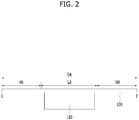
- FIG. 1 is a diagram showing a display area of a display device according to an embodiment and FIG. 2 is a cross-sectional view showing a superposition structure of the display area of a panel and an optical module, taken along line I-I' in the display area shown in FIG. 1 .
- An electroluminescent display may be applied as the display device according to an embodiment.
- an electroluminescent display an organic light emitting diode (OLED) display device, a quantum-dot light emitting diode display device, or an inorganic light emitting diode display device may be used.
- OLED organic light emitting diode
- quantum-dot light emitting diode display device a quantum-dot light emitting diode display device
- an inorganic light emitting diode display device may be used.
- the display device includes a panel 100 having a display area DA in which a plurality of pixels or unit pixels is arranged to display an image and a bezel area BZ surrounding the display area DA.
- the display area DA may be represented or referred to as a pixel array area or an active area.
- the bezel area BZ may be small or may be omitted.
- the panel 100 may further include a touch sensor screen superposed on the display area A to sense user touch, and the touch sensor screen may be embedded in the panel 100 or disposed on the display area DA of the panel 100.
- the display area DA of the panel 100 has a high-resolution area HA corresponding to a large part of the display area DA and a low-resolution area LA superposed on an optical module 110 disposed on the backside of the panel 100.
- the high-resolution area HA includes unit pixels and has high PPI (pixels per inch) and thus has a pixel arrangement structure with a high pixel density.
- the low-resolution area LA includes a pixel region (light emission region) corresponding to unit pixels and a transmission area for light transmission and has low PPI and thus has a pixel arrangement structure with a low pixel density.
- a pixel density may be defined as a number of unit pixels per unit area.
- the optical module 110 superposed on the low-resolution area LA can secure sufficient transmissivity for incident light or projected light thereof, which penetrates the low-resolution area LA, according to the transmission area of the low-resolution area LA.
- the area occupied by the transmission area be larger than the area occupied by the pixel region in the low-resolution area and it is desirable that the size of the low-resolution area LA be larger than the size of a region where the low-resolution area LA is superposed on the optical module 110, as shown in FIG. 2 .
- the optical module 110 using light penetrating the low-resolution area LA of the display area DA may be a camera module and may further include at least one of various optical sensors such as an infrared sensor, an illumination sensor, an RGB sensor and a fingerprint sensor.
- the display area DA of the panel 100 may include a single low-resolution area LA surrounded by the high-resolution area HA, as shown in FIG. 1(a) , and the optical module 110 using light penetrating the low-resolution area LA may be a camera module.
- the display area DA of the panel 100 may include a plurality of low-resolution areas LA surrounded by the high-resolution area HA, and a plurality of optical modules individually superposed on the plurality of low-resolution areas LA may include camera modules, illumination sensors, fingerprint sensors, and the like, as shown in FIG. 1(b) .
- the number of low-resolution areas LA disposed in the display area DA may be changed as necessary.
- the low-resolution area LA in the display area DA of the panel 100 may be used for various purposes as necessary.
- the display device which includes the low-resolution area LA having an octagonal shape, it is possible to improve definition deterioration due to visual recognition of a boundary area between the low-resolution area LA and the high-resolution area HA by arranging a transmission area in the boundary area in which outermost unit pixels of the high-resolution area HA neighboring the octagonal low-resolution area LA are positioned in different forms according to the inclination or slope of the respective boundary line of the boundary area instead of removing unit pixels. This will be described in detail later.
- the display device can improve definition deterioration due to visual recognition of the low-resolution area LA by compensating for the luminance of the low-resolution area LA having a lower pixel density, that is, a smaller number of unit pixels emitting light, than that of the high-resolution area HA to a level equivalent to that of the high-resolution area HA. This will be described in detail later.
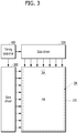
- FIG. 3 is a block diagram showing a circuit configuration of the display device according to an embodiment
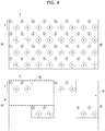
- FIG. 4 is a diagram showing pixel arrangement structures of a high-resolution area and a low-resolution area according to an embodiment
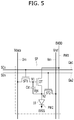
- FIG. 5 is an equivalent circuit diagram of a subpixel according to an embodiment.
- the display device includes the panel 100, a gate driver 200, a data driver 300, a timing controller 400, and the like.
- the gate driver 200 and the data driver 300 may be defined as a panel driver for driving the panel 100.
- the gate driver 200, the data driver 300 and the timing controller 400 may be defined as the driver for driving the panel 100.
- the display area DA of the panel 100 includes a plurality of unit pixels, and each unit pixel displays an image using red (R), green (G) and blue (B) subpixels.
- each unit pixel P may be composed of four subpixels RGBG.
- red (R) subpixels and blue (B) subpixels other than green (G) subpixels may be alternately arranged in the horizontal direction and the vertical direction.
- the display area DA of the panel 100 has a high-resolution area HA and a low-resolution area LA superposed on the optical module 110 disposed on the backside of the panel 100.
- the high-resolution area HA having high PPI has a pixel arrangement structure composed of unit pixels P.
- the low-resolution area LA having low PPI has a pixel arrangement structure including pixel areas PA each corresponding to a unit pixel P and a transmission area TA disposed adjacent to the pixel area PA and having a low pixel density.
- the PPI of the low-resolution area LA may be a quarter that of the high-resolution area HA.
- the unit pixel P may have the same size in the high-resolution area HA and the low-resolution area LA.
- each mask area M has a pixel area PA corresponding to a single unit pixel P and a transmission area corresponding to an area in which three unit pixels are removed, and thus the transmission area TA may have an area larger than the pixel area PA.
- the low-resolution area LA may have one unit pixel P per area of four unit pixels and a transmission area TA corresponding to the area of three unit pixels.
- the transmission area TA may be an area where no unit pixels P are arranged.
- each pixel area PA may be disposed in a (4k-3)-th row (k being a positive integer) in any one of odd-numbered columns and even-numbered columns and disposed in a (4k-1)-th row in other columns, and the transmission area TA may be disposed in the remaining area. Accordingly, the optical module on which the low-resolution area LA is superposed can secure sufficient light transmissivity through the transmission area TA larger than the pixel area PA to provide high performance of a camera or an optical sensor.
- Each subpixel SP includes an emission element and a pixel circuit for independently driving the emission element.
- An organic light emitting diode, a quantum-dot light emitting diode, or an inorganic light emitting diode may be applied as the emission element.
- the pixel circuit includes a plurality of TFTs including at least a driving TFT for driving the emission element and a switching TFT for supplying a data signal to the driving TFT, and a storage capacitor which stores a driving voltage Vgs corresponding to the data signal supplied through the switching TFT and provides the driving voltage Vgs to the driving TFT.
- the pixel circuit may further include a plurality of TFTs which initializes three electrodes (a gate, a source and a drain) of the driving TFT, connects the driving TFT in a diode structure for threshold voltage compensation, or controls an emission time of the emission element.
- TFTs which initializes three electrodes (a gate, a source and a drain) of the driving TFT, connects the driving TFT in a diode structure for threshold voltage compensation, or controls an emission time of the emission element.
- 3T1C 3 TFTs and 1 capacitor
- 7T1C (7 TFTs and 1 capacitor) may be applied as a pixel circuit configuration.
- each subpixel SP has a pixel circuit including at least an emission element 10 connected between a power line through which a high driving voltage (first driving voltage; EVDD) is supplied and a common electrode through which a low driving voltage (second driving voltage; EVSS) is supplied, and first and second switching TFTs ST1 and ST2, a driving TFT DT and a storage capacitor Cst for independently driving the emission element 10, as shown in FIG. 5 .
- first driving voltage first driving voltage
- EVSS low driving voltage
- first and second switching TFTs ST1 and ST2 a driving TFT DT and a storage capacitor Cst for independently driving the emission element 10, as shown in FIG. 5 .
- the emission element 10 includes an anode connected to a source node N2 of the driving TFT DT, a cathode connected to an EVSS line PW2, and an organic emission layer formed between the anode and the cathode.
- the anode is independently provided for each subpixel but the cathode may be a common electrode shared by all subpixels.
- the emission element 10 generates light with brightness proportional to a value of driving current in such a manner that electrons from the cathode are injected into the organic emission layer and holes from the anode are injected into the organic emission layer when the driving current is supplied from the driving TFT DT and fluorescent or phosphorescent materials are emitted according to recombination of the electrons and the holes in the organic emission layer.
- the first switching TFT ST1 is driven by a scan pulse signal SCn supplied from the gate driver 200 to a gate line Gn1 and transmits a data voltage Vdata supplied from the data driver 300 to a data line Dm to a gate node N1 of the driving TFT DT.
- the second switching TFT ST2 is driven by a sense pulse signal SEn supplied from the gate driver 200 to another gate line Gn2 and transmits a reference voltage Vref supplied from the data driver 300 to a reference line Rm to the source node N2 of the driving TFT DT.
- the second switching TFT ST2 can provide current in which characteristics of the driving TFT DT or characteristics of the emission element 10 are reflected to the reference line Rm
- the storage capacitor Cst connected between the gate node N1 and the source node N2 of the driving TFT DT charges a difference voltage between the data voltage Vdata and the reference voltage Vref respectively supplied to the gate node N1 and the source node N2 through the first and second switching TFTs ST1 and ST2 as the driving voltage Vgs of the driving TFT DT and holds the charged driving voltage Vgs for an emission period in which the first and second switching TFTs ST1 and ST2 are turned off.
- the driving TFT DT causes the emission element 10 to emit light by controlling a current supplied through an EVDD line PW1 according to the driving voltage Vgs supplied from the storage capacitor Cst to provide a driving current determined by the driving voltage Vgs to the emission element 10.
- the gate driver 200 is controlled by a plurality of gate control signals supplied from the timing controller 400 and individually drives gate lines of the panel 100.
- the gate driver 200 provides a scan signal of a gate on voltage to a corresponding gate line in a driving period of the gate line and provides a gate off voltage to the gate line in a non-driving period of the gate line.
- the data driver 300 is controlled by data control signals supplied from the timing controller 400, converts digital data supplied from the timing controller 400 into analog data signal and provides a corresponding data signal to each data line of the panel 100.
- the data driver 300 converts the digital data into the analog data signal using grayscale voltages obtained by subdividing a plurality of reference gamma voltages supplied from a gamma voltage generator.
- the data driver 300 can provide the reference voltage to the reference line.
- the data driver 300 can provide a data voltage for sensing to data lines to drive pixels according to control of the timing controller 400, sense a pixel current representing electrical characteristics of the driven pixels as a voltage through the reference line Rm, convert the voltage into digital sensing data and provide the digital sensing data to the timing controller 400 in the sensing mode.
- the timing controller 400 controls the gate driver 200 and the data driver 300 using timing control signals supplied from an external system and timing setting information stored therein.
- the timing control signals may include a dot clock signal, a data enable signal, a vertical synchronization signal, a horizontal synchronization signal, and the like.
- the timing controller 400 generates a plurality of gate control signals for controlling driving timing of the gate driver 200 and provides the gate control signals to the gate driver 200.
- the timing controller 400 generates a plurality of data control signals for controlling driving timing of the data driver 300 and provides the data control signals to the data driver 300.
- the driver or timing controller 400 may perform various types of image processing on received input image data and output the processed data to the data driver 300.
- the timing controller 400 can improve recognized definition of the low-resolution area LA by applying different weights to colors to compensate for a luminance deviation of the low-resolution area LA having lower pixel density than that of the high-resolution area HA to a level equivalent to that of the high-resolution area HA. This will be described in detail later.
- the timing controller 400 can analyze image data and control maximum luminance according to an average picture level (APL) to reduce power consumption.
- APL average picture level
- the timing controller 400 may further perform definition enhancement processing such as compensation of initial characteristic deviation of each pixel and deterioration (image sticking) compensation on image data.
- the timing controller 400 may drive the panel 100 in the sensing mode by controlling the gate driver 200 and the data driver 300 and execute a function of sensing a threshold voltage of the driving TFT DT, mobility of the driving TFT DT and a threshold voltage of the emission element 10, in which characteristic deviation and deterioration of each pixel of the panel 100 have been reflected, through the data driver 300.
- the timing controller 400 can perform definition enhancement processing for compensating for characteristic deviation and deterioration of each pixel using a sensing result.
- the timing controller 400 may accumulate data used in each subpixel as stress data and further perform definition enhancement processing for compensating for deterioration of each subpixel according to the accumulated stress data.
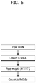
- FIG. 6 is a flowchart showing a method of compensating for the luminance of a low-resolution area of the display device according to an embodiment, which is performed by the timing controller 400 shown in FIG. 3 .
- the driver or timing controller 400 receives image data such as source 3-color data RiGiBi with respect to the low-resolution area LA and converts the source 3-color data RiGiBi into 4-color data WRGB using an RGB-to-WRGB (3 colors-to-4 colors) conversion method.
- the driver or timing controller 400 converts the source 3-color data RiGiBi into the 4-color data WRGB by generating W data from a minimum value of the source 3-color data RiGiBi and subtracting the W data from RiGiBi data to generate RGB data as represented by Mathematical Expression 1.
- the driver or timing controller 400 derives compensated 4-color data W'R'G'B' by applying color weights Weight_W, Weight_R, Weight_G and Weight_B to the converted 4-color data WRGB, as represented by Mathematical Expression 2, converts the compensated 4-color data W'R'G'B' into compensated R'G'B' data and outputs the compensated R'G'B'.
- the maximum gray range (WRGB Max Gray Range) which can be compensated for according to Mathematical Expression 2 can be calculated as 135 gray. Accordingly, luminance compensation in which the color weights Weight_W, Weight_R, Weight_G and Weight_B are applied to WRGB data with respect to the low-resolution area LA can be performed only on WRGB data corresponding to 0 to 135 gray values and may not be performed on high gray values exceeding 135 gray.
- the color weights Weight_W, Weight_R, Weight_G and Weight_B are luminance compensation values determined in order to compensate for luminance differences. Accordingly, when the weights Weight_W, Weight_R, Weight_G and Weight_B are applied to WRGB data that is gray values, de-gamma is applied and de-gamma color weights Weight_W 1/2.2 , Weight_R 1/2.2 and Weight_G 1/2.2 , Weight_B 1/2.2 are applied to the WRGB data for the colors.
- the color weights Weight_W, Weight_R, Weight_G and Weight_B are determined to be equal to or less than a maximum weight of WRGB (WRGB Weight Max).
- the maximum weight of WRGB (WRGB Weight Max) may be determined as the ratio of the number of unit pixels, Low_N, in the mask area M in the low-resolution area LA to the number of unit pixels, High_N, in the mask area M in the high-resolution area HA, as represented by Mathematical Expression 2. For example, when the ratio of the number of unit pixels, Low_N, in the mask area M in the low-resolution area LA to the number of unit pixels, High_N, in the mask area M in the high-resolution area HA is 1/4, as shown in FIG. 4 , the maximum weight of WRGB (WRGB Weight Max) can be 4 and the color weights Weight_W, Weight_R, Weight_G and Weight_B can be determined to be equal to or less than 4.
- the color weights Weight_W, Weight_R, Weight_G and Weight_B in Mathematical Expression 2 can be derived as shown in the graph of FIG. 8 on the basis of a recognition evaluation pattern and an evaluation method shown in FIG. 7 .
- luminance differences of the low-resolution area LA in contrast to the high-resolution area HA can be measured for colors and gray values on the basis of luminance recognition evaluation using an evaluation pattern in which low-resolution areas LA expressing 256 gray values of 0 to 255 for a plurality of gray values (32, 64, 96, 128, 160) of the high-resolution area HA are displayed. Then, color weights Weight_W, Weight_R, Weight_G and Weight_B having luminance percentages of the low-resolution area LA to the high-resolution area HA can be derived as compensation values as shown in a linear function graph of FIG. 8 . Referring to FIG.
- R weight Weight_R and B weight Weight_B need to be greater than G weight Weight_G in order to reduce a luminance difference of the low-resolution area LA in contrast to the high-resolution area HA.
- R/B data needs a higher luminance increase rate than G data in order to reduce luminance differences of the low-resolution area LA in contrast to the high-resolution area HA.
- W weight Weight_W is greater than G weight Weight_G and less than B weight Weight B.
- FIG. 9 is a diagram showing luminance compensation effects of a low-resolution area using a luminance compensation method according to an embodiment.
- FIG. 9 it can be ascertained that luminance deterioration in low-resolution areas LA is recognized before luminance compensation using color weights according to an embodiment is performed on the low-resolution areas LA, as shown in FIG. 9(a) and (b) .
- the timing controller 400 compensates for the luminance of the low-resolution areas LA by applying color weights according to an embodiment thereto, the luminance of the low-resolution areas is improved to a level equivalent or similar to that of high-resolution areas such that luminance deterioration in the low-resolution areas is not visually recognized, as shown in FIG. 9(c) and (d) .
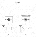
- FIG. 10 is a diagram showing smoothing processing performed on a boundary area of a low-resolution area having a high grayscale according to an embodiment.
- an image with a high grayscale on which luminance compensation cannot be performed may be displayed in a low-resolution area LA, as described above.
- a luminance difference between the low-resolution area and a high-resolution area may be markedly recognized in the boundary area, as shown in FIG. 10(a) .
- the timing controller 400 can apply smoothing image processing of gradually reducing luminance according to pixel position from the high-resolution area to the low-resolution area, as shown in FIG. 10(b) . Consequently, it can be ascertained that a luminance difference between the high-resolution area and the low-resolution area is gradually improved according to pixel position.
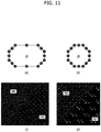
- FIG. 11 is a diagram showing an octagonal low-resolution area according to an embodiment.
- a low-resolution area LA has an octagonal shape, as shown in FIG. 11(a) and (b) , such that a pixel arrangement structure at a boundary between the low-resolution area LA and a high-resolution area HA for preventing visual recognition of the boundary can be designed. It can be ascertained that a luminance deviation or color variation between the high-resolution area HA and the low-resolution area LA is uniform when the octagonal low-resolution area LA has the same slope in the boundary area, as shown in FIG. 11(c) and (d) .
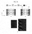
- FIGS. 12 to 14 are diagrams showing pixel arrangement structures in a boundary area between a high-resolution area and a low-resolution area according to boundary slopes according to an embodiment.
- outermost unit pixels RGBG of the high-resolution area neighboring the low-resolution area LA may be defined as unit pixels of a boundary area BA.
- the boundary area BA of the high-resolution area may be defined as the unit pixel areas directly neighboring the low-resolution area LA.
- the boundary area BA of the high-resolution area HA neighboring the low-resolution area LA includes first to eighth boundary sub-areas BA1 to BA8 along respective boundary lines having slopes of 0°, 45°, 135° and 90° in the x-axis direction.
- a slope of the first to eight boundary sub-areas BA1 to BA8 may be defined as the inclination of the respective boundary line being a straight line having a certain angle to the x-axis direction and/or the y-axis direction.
- transmission areas TA are disposed according to the slopes of corresponding boundary sub-areas without removing unit pixels of the boundary area BA at regular intervals, that is boundary sub-areas where unit pixels are not removed, i.e. consecutively arranged.
- the first to eighth boundary sub-areas BA1 to BA8 may include one unit pixel per area of two unit pixels and a transmission area corresponding to one unit pixel area or three unit pixels per area of four unit pixels and a transmission area corresponding to one unit pixel area according to the slopes thereof.
- the first to eighth boundary sub-areas BA1 to BA8 have PPI higher than that of the low-resolution area LA and lower than that of the high-resolution area HA.
- the first and second boundary sub-areas BA1 and BA2 of the high-resolution area HA adjacent to unit pixels of the low-resolution area LA are positioned at an inclination of 0° in the x-axis direction and face each other in the y-axis direction.
- the first and second boundary sub-areas BA1 and BA2 include one unit pixel per area of two unit pixels, and a transmission area corresponding to one unit pixel area which are positioned in the x-axis direction.
- the first and second boundary sub-areas BA1 and BA2 have a structure in which a (2k-1)-th unit pixel or a 2k-th unit pixel among two unit pixels neighboring in the x-axis direction is removed and the transmission area TA is disposed in the corresponding region.
- the (2k-1)-th unit pixel is removed and the transmission area TA may be disposed in the corresponding region in the first boundary sub-area BA1, and the 2k-th unit pixel is removed and the transmission area TA may be disposed in the corresponding region in the second boundary sub-area BA2.
- the 2k-th unit pixel is removed and the transmission area TA may be disposed in the corresponding region in the first boundary sub-area BA1
- the (2k-1)-th unit pixel is removed and the transmission area TA may be disposed in the corresponding region in the second boundary sub-area BA2.
- the unit pixels disposed in the first and second boundary sub-areas BA1 and BA2 may be arranged in a 45° diagonal direction with respect to unit pixels of the neighboring low-resolution area LA.
- the transmission areas TA disposed in the first and second boundary sub-areas BA1 and BA2 may be arranged in a 45° diagonal direction with respect to the unit pixels of the neighboring low-resolution area LA.
- the third and fourth boundary sub-areas BA3 and BA4 of the high-resolution area HA adjacent to the unit pixels of the low-resolution area LA are positioned in a first diagonal direction at an inclination of 45° with respect to the x-axis direction
- the fifth and sixth boundary sub-areas BA5 and BA6 are positioned in a second diagonal direction at an inclination of 135° with respect to the x-axis direction.
- the third and fourth boundary sub-areas BA3 and BA4 face each other in the second diagonal direction
- the fifth and sixth boundary sub-areas BA5 and BA6 face each other in the first diagonal direction.
- the third to sixth boundary sub-areas BA3, BA4, BA5 and BA6 include one unit pixel per area of two unit pixels, and a transmission area TA corresponding to one unit pixel area which are positioned in the first or second diagonal direction.
- the third and fourth boundary sub-areas BA3 and BA4 have a structure in which a (2k-1)-th unit pixel or a 2k-th unit pixel among two unit pixels neighboring in the 45° first diagonal direction is removed and the transmission area TA is disposed in the corresponding region.
- the fifth and sixth boundary sub-areas BA5 and BA6 have a structure in which a (2k-1)-th unit pixel or a 2k-th unit pixel among two unit pixels neighboring in the 135° second diagonal direction is removed and the transmission area TA is disposed in the corresponding region.
- the (2k-1)-th unit pixel between two unit pixels neighboring in the first or second diagonal direction is removed and the transmission area TA may be disposed in the corresponding region in the third to sixth boundary sub-areas BA3, BA4, BA5 and BA6.
- the 2k-th unit pixel between two unit pixels neighboring in the first or second diagonal direction is removed and the transmission area TA may be disposed in the corresponding region in the third to sixth boundary sub- areas BA3, BA4, BA5 and BA6.
- the unit pixels disposed in the third to sixth boundary sub-areas BA3, BA4, BA5 and BA6 may be arranged in a 45° or 135° diagonal direction with respect to the unit pixels of the neighboring low-resolution area LA.
- the transmission areas TA disposed in the third to sixth boundary sub-areas BA3, BA4, BA5 and BA6 may be arranged adjacent to the unit pixels of the neighboring low-resolution area LA in the x-axis direction.
- the seventh and eighth boundary sub- areas BA7 and BA8 of the high-resolution area HA adjacent to the unit pixels of the low-resolution area LA are positioned in the y-axis direction at an inclination of 90° with respect to the x-axis direction and face each other in the x-axis direction.
- the seventh and eighth boundary sub-areas BA7 and BA8 include three unit pixels per area of four unit pixels, and a transmission area corresponding to one unit pixel area which are positioned in the y-axis direction.
- the seventh and eighth boundary sub-areas BA7 and BA8 have a structure in which a (4k-3)-th unit pixel or a 4k-th unit pixel among four unit pixels disposed in the y-axis direction is removed and the transmission area TA is disposed in the corresponding region.
- the (4k-3)-th unit pixel among four unit pixels disposed in the y-axis direction is removed and the transmission area TA may be disposed in the corresponding region in the seventh boundary sub-area BA7.
- the 4k-th unit pixel among four unit pixels disposed in the y-axis direction is removed and the transmission area TA may be disposed in the corresponding region in the eighth boundary sub-area BA8.
- the 4k-th unit pixel among four unit pixels disposed in the y-axis direction is removed and the transmission area TA may be disposed in the corresponding region in the seventh boundary sub-area BA7, and the (4k-3)-th unit pixel among four unit pixels disposed in the y-axis direction is removed and the transmission area TA may be disposed in the corresponding region in the eighth boundary sub-area BA8.
- the unit pixels disposed in the seventh boundary sub-area BA7 may be arranged adjacent to the unit pixels of the neighboring low-resolution area LA in the x-axis direction, and the transmission areas TA disposed in the seventh boundary sub-area BA7 may be arranged adjacent to the unit pixels of the neighboring low-resolution area LA in the x-axis direction.
- the unit pixels disposed in the eighth boundary sub-area BA7 may be arranged adjacent to transmission areas or unit pixels of the neighboring low-resolution area LA in the x-axis direction, and the transmission areas TA disposed in the eighth boundary sub-area BA8 may be arranged adjacent to the transmission areas of the neighboring low-resolution area LA in the x-axis direction.
- FIGS. 15 to 17 are diagrams showing optimal pixel arrangement structures at a boundary and luminance compensation effects of a low-resolution area according to an embodiment.
- unit pixels on which luminance compensation has been performed in a low-resolution area LA immediately neighbor unit pixels of a high-resolution area HA and thus a bright line defect may be generated at the boundary of the low-resolution area LA when the embodiment of the pixel arrangement structure for a boundary described in FIGS. 12 to 14 is not applied.
- a boundary of a low-resolution area LA is visually recognized as a bright line defect in a general image and a 128-gray image if unit pixels on which luminance compensation has been performed in the low-resolution area LA immediately neighbor unit pixels of a high-resolution area HA when the embodiment of the pixel arrangement structure for a boundary described in FIGS. 12 to 14 is not applied.
- the boundary of the low-resolution area LA is visually recognized as a dark line defect in the general image and the 128-gray image if only transmission areas in the low-resolution area LA immediately neighbor the unit pixels of the high-resolution area HA when the embodiment of the pixel arrangement structure for a boundary described in FIGS. 12 to 14 is not applied.
- the boundary of the low-resolution area LA is not visually recognized and luminance deterioration in the low-resolution area LA is improved in the general image and the 128-gray image when both luminance compensation for the low-resolution area LA and the embodiment of the pixel arrangement structure for a boundary described in FIGS. 12 to 14 are applied.
- the display device can prevent the boundary area of a low-resolution area from being visually recognized and improve definition deterioration in the low-resolution area by compensating for the luminance of the low-resolution area and differently arranging unit pixels and transmission areas in the boundary area of a high-resolution area adjacent to the low-resolution area having an octagonal shape according to slopes of the boundary area, thereby enhancing overall definition.
Landscapes
- Engineering & Computer Science (AREA)
- Physics & Mathematics (AREA)
- Computer Hardware Design (AREA)
- General Physics & Mathematics (AREA)
- Theoretical Computer Science (AREA)
- Control Of Indicators Other Than Cathode Ray Tubes (AREA)
- Devices For Indicating Variable Information By Combining Individual Elements (AREA)
- Control Of El Displays (AREA)
- Electroluminescent Light Sources (AREA)
Abstract
Description
- This application claims the priority of Korean Patent Application No.
10-2020-0011855, filed on January 31, 2020 - The present disclosure relates to a display device capable of improving definition of a low-resolution area in a display area having a high-resolution area and the low-resolution area.
- Electronic devices such as smartphones and tablets are equipped with an optical module, for example, a camera module, along with a display device.
- Although a camera module is generally disposed under a through-hole penetrating a bezel of an electronic device, there is demand for a structure in which a camera module is disposed on the backside of a display area of a display device and light transmission in the display area is used since a bezel size has recently decreased in order to extend the display area.
- A region superposed on the camera module in the display area needs to have low resolution such that sufficient light transmissivity can be secured.
- When the display area has a high-resolution area and a low-resolution area, there are problems that a boundary area between the high-resolution area and the low-resolution area is visually recognizable and definition deterioration of visual recognition of the low-resolution area due to luminance deterioration in the low-resolution area.
- It is an object of the present disclosure to provide a display device capable of improving definition deterioration due to recognition of a boundary area of a low-resolution area superposed on an optical module in a display area and enhancing the definition of the low-resolution area to a recognition level equivalent to that of a high-resolution area.
- This object is solved by the subject-matter of the independent claim. Further advantageous embodiments and refinements are described in the respective dependent claims.
- A display device according to an embodiment includes: a panel including a display area in which a plurality of pixels is arranged; and an optical module superposed on the display area, wherein the display area has a low-resolution area having a polygonal shape and superposed on the optical module and a high-resolution area neighboring the low-resolution area, in the low-resolution area, unit pixels having the same size as those of the high-resolution area are arranged in a lower pixel density than that of the high-resolution area and transmission areas are disposed adjacent to the unit pixels, and unit pixels and transmission areas are arranged in different forms in a boundary area of the high-resolution area neighboring the low-resolution area according to the shape, i.e. to slopes or inclinations of the boundary lines, of the boundary area.
- The display device according to embodiments of the present invention may comprise one or several of the following optional features.
- The optical module may use light penetrating the low-resolution area of the display area. The optical module may include a camera module and/or may include at least one of various optical sensors such as an infrared sensor, an illumination sensor, an RGB sensor and a fingerprint sensor. The optical module may be disposed on the backside of the panel.
- A pixel density may be defined as a number of unit pixels per unit area, for example a unit area of the display area.
- The slopes or inclinations of the boundary lines of the boundary area may be formed according to the shape of the low-resolution area. The boundary area of the high-resolution area may be defined as the unit pixel areas directly neighboring the low-resolution area. For example, the slope of a boundary line may include a straight line having a certain angle to a horizontal direction and/or to a vertical direction. Thus, the boundary lines of the boundary area may surround a polygonal shape of the low-resolution area. In the boundary area according to embodiments of the present invention, unit pixels are removed and transmission areas are disposed in the corresponding regions of the removed unit pixels compared to an area where unit pixels are not removed, i.e. consecutively arranged. Thus, the boundary area may have a pixel density higher than that of the low-resolution area and lower than that of the high-resolution area.
- The transmission area may be an area where no unit pixels are arranged.
- The low-resolution area may have an octagonal shape. The boundary area of the high-resolution area may have a plurality of boundary sub-areas having different slopes. That is, the boundary area of the high-resolution area may include a plurality of sub-areas along respective boundary lines having different inclinations.
- The plurality of boundary sub-areas of the high-resolution area may include first and second boundary sub-areas disposed in an x-axis direction (the horizontal or first direction) and facing each other in a y-axis direction (the vertical or second direction). The first and second boundary sub-areas may include one unit pixel per area of two unit pixels and a transmission area corresponding to each unit pixel area positioned in the x-axis direction. Thus, in the first and second boundary sub-areas, one unit pixel and one transmission area are alternately arranged along the respective boundary line. A position of a transmission area per area of two unit pixels in the first boundary area may be opposite to a position of a transmission area per area of two unit pixels in the second boundary area. The horizontal or first direction and the vertical or second direction may be arranged in parallel to the surface of the display area and may be defined to be perpendicular to each other.
- The plurality of boundary sub-areas of the high-resolution area may include third and fourth boundary sub-areas disposed in a first diagonal direction at an inclination of 45° to the x-axis direction and fifth and sixth boundary sub-areas disposed in a second diagonal direction at an inclination of 135° to the x-axis direction. The third and fourth boundary sub-areas may include one unit pixel per area of two unit pixels and a transmission area corresponding to each unit pixel area positioned in the first diagonal direction. The fifth and sixth boundary sub-areas may include one unit pixel per area of two unit pixels and a transmission area corresponding to each unit pixel area positioned in the second diagonal direction. The transmission area per area of two unit pixels may be disposed at the same position in the third to sixth boundary sub-areas. Thus, in the third to sixth boundary sub-areas, one unit pixel and one transmission area are alternately arranged along the respective boundary line.
- The plurality of boundary sub-areas of the high-resolution area may include seventh and eighth boundary sub-areas disposed in the y-axis direction and facing each other in the x-axis direction. The seventh and eighth boundary sub-areas may include three unit pixels per area of four unit pixels and a transmission area corresponding to each unit pixel area positioned in the y-axis direction. A position of a transmission area per area of four unit pixels in the seventh boundary area may be different from a position of a transmission area per area of four unit pixels in the eighth boundary area. Thus, in the seventh and eigth boundary sub-areas, three unit pixels are consecutively arranged along the respective boundary line and the three unit pixels and one transmission area are alternately arranged along the respective boundary line.
- A transmission area of the seventh boundary area may be positioned in the area of the first unit pixel per area of four unit pixels in the seventh boundary area. A transmission area of the eighth boundary area may be positioned in the area of the fourth unit pixel per area of four unit pixels in the eighth boundary area.
- The low-resolution area may include one unit pixel per area of four unit pixels and a transmission area corresponding to three unit pixel areas.
- The area of the low-resolution area may be larger than the area of a region where the low-resolution area is superposed on the optical module.
- The display area may include a plurality of low-resolution areas superposed on a plurality of optical modules.
- The display device may include a driver for driving the panel. The driver or timing controller comprised in the driver may compensate for luminance by applying different weights for colors to image data of the low-resolution area. The different color weights may be derived using proportions of luminances for colors of the low-resolution area to those of the high-resolution area using results of measurement of luminance differences for colors in the low-resolution area in contrast to the high-resolution area.
- The driver or timing controller may convert input 3-color (RGB) data for the low-resolution area into 4-color (WRGB) data, apply the color weights to the converted 4-color data to generate corrected 4-color data, convert the corrected 4-color data into corrected 3-color data, and may output the corrected 3-color data.
- The color weights may be less than a maximum weight using a ratio of the number of unit pixels per mask area of the high-resolution area to the number of unit pixels per mask area of the low-resolution area. A mask area may be defined as an area having a size of n∗n, e.g. 2∗2, unit pixels along the horizontal direction and the vertical direction, respectively. Therein, n may be an integer.
- The driver or timing controller may perform de-gamma processing on the color weights and apply the de-gamma processed color weights to the converted 4-color data.
- A red weight and a blue weight among the color weights may be greater than a green weight, and a white weight may be greater than the green weight and less than the blue weight.
- The driver or timing controller may derive a maximum gray range that is able to be compensated using the color weights using a ratio of the number of unit pixels per mask area of the low-resolution area to the number of unit pixels per mask area of the high-resolution area in image data of the low-resolution area, and perform luminance compensation on grays equal to or greater than 0 gray and equal to or less than the maximum gray range that is able to be compensated using the color weights.
- The driver or timing controller may perform luminance compensation on high-gray data exceeding the maximum gray range that is able to be compensated by applying smoothing processing of gradually reducing luminance from the high-resolution area to the low-resolution area to the high-gray data.
- The display device according to an embodiment can prevent visual recognition of a boundary area of a low-resolution area and improve definition deterioration in the low-resolution area by compensating for the luminance of the low-resolution area and differently arranging unit pixels and transmission areas in a boundary area of a high-resolution area neighboring the low-resolution area having an octagonal shape according to slopes of the boundary area, thereby improving the entire definition.
-
-
FIG. 1 is a diagram showing a display area of a display device according to an embodiment. -
FIG. 2 is a cross-sectional view showing a superposition structure of the display area and an optical module, taken along line I-I' in the display area shown inFIG. 1 . -
FIG. 3 is a block diagram showing a circuit configuration of the display device according to an embodiment. -
FIG. 4 is a diagram showing pixel arrangement structures of a high-resolution area and a low-resolution area according to an embodiment. -
FIG. 5 is an equivalent circuit diagram of a subpixel according to an embodiment. -
FIG. 6 is a flowchart showing a method of compensating for luminance of the display device according to an embodiment. -
FIG. 7 is a diagram showing a luminance deviation evaluation pattern and an evaluation method for a low-resolution area in contrast to a high-resolution area according to an embodiment. -
FIG. 8 is a graph showing results of derivation of a maximum compensation amount for each color for luminance compensation of a low-resolution area in contrast to a high-resolution area according to an embodiment. -
FIG. 9 is a diagram showing luminance compensation effects of a low-resolution area according to an embodiment. -
FIG. 10 is a diagram showing smoothing processing performed on a boundary area of a low-resolution area having a high grayscale according to an embodiment. -
FIG. 11 is a diagram showing an octagonal low-resolution area according to an embodiment. -
FIG. 12 is a diagram showing a pixel arrangement structure at a boundary area between a high-resolution area and a low-resolution area in an x direction according to an embodiment. -
FIG. 13 is a diagram showing a pixel arrangement structure at a boundary area between a high-resolution area and a low-resolution area in diagonal directions according to an embodiment. -
FIG. 14 is a diagram showing a pixel arrangement structure at a boundary area between a high-resolution area and a low-resolution area in a y direction according to an embodiment. -
FIG. 15 is a diagram showing optimal pixel arrangement in a boundary area and luminance compensation effects of a low-resolution area according to an embodiment. -
FIG. 16 is a diagram showing optimal pixel arrangement in a boundary area and luminance compensation effects of a low-resolution area according to an embodiment. -
FIG. 17 is a diagram showing optimal pixel arrangement in a boundary area and luminance compensation effects of a low-resolution area for each color image according to an embodiment. - Hereinafter, preferred embodiments of the present disclosure will be described with reference to the drawings.
-
FIG. 1 is a diagram showing a display area of a display device according to an embodiment andFIG. 2 is a cross-sectional view showing a superposition structure of the display area of a panel and an optical module, taken along line I-I' in the display area shown inFIG. 1 . - An electroluminescent display may be applied as the display device according to an embodiment. As an electroluminescent display, an organic light emitting diode (OLED) display device, a quantum-dot light emitting diode display device, or an inorganic light emitting diode display device may be used.
- Referring to
FIGS. 1 and2 , the display device according to an embodiment includes apanel 100 having a display area DA in which a plurality of pixels or unit pixels is arranged to display an image and a bezel area BZ surrounding the display area DA. The display area DA may be represented or referred to as a pixel array area or an active area. The bezel area BZ may be small or may be omitted. Thepanel 100 may further include a touch sensor screen superposed on the display area A to sense user touch, and the touch sensor screen may be embedded in thepanel 100 or disposed on the display area DA of thepanel 100. - The display area DA of the
panel 100 has a high-resolution area HA corresponding to a large part of the display area DA and a low-resolution area LA superposed on anoptical module 110 disposed on the backside of thepanel 100. The high-resolution area HA includes unit pixels and has high PPI (pixels per inch) and thus has a pixel arrangement structure with a high pixel density. The low-resolution area LA includes a pixel region (light emission region) corresponding to unit pixels and a transmission area for light transmission and has low PPI and thus has a pixel arrangement structure with a low pixel density. A pixel density may be defined as a number of unit pixels per unit area. - The
optical module 110 superposed on the low-resolution area LA can secure sufficient transmissivity for incident light or projected light thereof, which penetrates the low-resolution area LA, according to the transmission area of the low-resolution area LA. To secure the light transmissivity of theoptical module 110, it is desirable that the area occupied by the transmission area be larger than the area occupied by the pixel region in the low-resolution area and it is desirable that the size of the low-resolution area LA be larger than the size of a region where the low-resolution area LA is superposed on theoptical module 110, as shown inFIG. 2 . - The
optical module 110 using light penetrating the low-resolution area LA of the display area DA may be a camera module and may further include at least one of various optical sensors such as an infrared sensor, an illumination sensor, an RGB sensor and a fingerprint sensor. - For example, the display area DA of the
panel 100 may include a single low-resolution area LA surrounded by the high-resolution area HA, as shown inFIG. 1(a) , and theoptical module 110 using light penetrating the low-resolution area LA may be a camera module. The display area DA of thepanel 100 may include a plurality of low-resolution areas LA surrounded by the high-resolution area HA, and a plurality of optical modules individually superposed on the plurality of low-resolution areas LA may include camera modules, illumination sensors, fingerprint sensors, and the like, as shown inFIG. 1(b) . The number of low-resolution areas LA disposed in the display area DA may be changed as necessary. In addition, the low-resolution area LA in the display area DA of thepanel 100 may be used for various purposes as necessary. - In the display device according to an embodiment which includes the low-resolution area LA having an octagonal shape, it is possible to improve definition deterioration due to visual recognition of a boundary area between the low-resolution area LA and the high-resolution area HA by arranging a transmission area in the boundary area in which outermost unit pixels of the high-resolution area HA neighboring the octagonal low-resolution area LA are positioned in different forms according to the inclination or slope of the respective boundary line of the boundary area instead of removing unit pixels. This will be described in detail later.
- Furthermore, the display device according to an embodiment can improve definition deterioration due to visual recognition of the low-resolution area LA by compensating for the luminance of the low-resolution area LA having a lower pixel density, that is, a smaller number of unit pixels emitting light, than that of the high-resolution area HA to a level equivalent to that of the high-resolution area HA. This will be described in detail later.
-
FIG. 3 is a block diagram showing a circuit configuration of the display device according to an embodiment,FIG. 4 is a diagram showing pixel arrangement structures of a high-resolution area and a low-resolution area according to an embodiment, andFIG. 5 is an equivalent circuit diagram of a subpixel according to an embodiment. - Referring to
FIG. 3 , the display device includes thepanel 100, agate driver 200, adata driver 300, atiming controller 400, and the like. Thegate driver 200 and thedata driver 300 may be defined as a panel driver for driving thepanel 100. Also, thegate driver 200, thedata driver 300 and thetiming controller 400 may be defined as the driver for driving thepanel 100. - The display area DA of the
panel 100 includes a plurality of unit pixels, and each unit pixel displays an image using red (R), green (G) and blue (B) subpixels. As shown inFIG. 4 , each unit pixel P may be composed of four subpixels RGBG. In an RGBG pixel arrangement structure shown inFIG. 4 , red (R) subpixels and blue (B) subpixels other than green (G) subpixels may be alternately arranged in the horizontal direction and the vertical direction. - The display area DA of the
panel 100 has a high-resolution area HA and a low-resolution area LA superposed on theoptical module 110 disposed on the backside of thepanel 100. - Referring to
FIG. 4 , the high-resolution area HA having high PPI has a pixel arrangement structure composed of unit pixels P. The low-resolution area LA having low PPI has a pixel arrangement structure including pixel areas PA each corresponding to a unit pixel P and a transmission area TA disposed adjacent to the pixel area PA and having a low pixel density. The PPI of the low-resolution area LA may be a quarter that of the high-resolution area HA. The unit pixel P may have the same size in the high-resolution area HA and the low-resolution area LA. - When a mask area M having a size of 2∗2 unit pixels is defined in the low-resolution area LA and/or in the high-resolution area HA, each mask area M has a pixel area PA corresponding to a single unit pixel P and a transmission area corresponding to an area in which three unit pixels are removed, and thus the transmission area TA may have an area larger than the pixel area PA. In other words, the low-resolution area LA may have one unit pixel P per area of four unit pixels and a transmission area TA corresponding to the area of three unit pixels. The transmission area TA may be an area where no unit pixels P are arranged.
- For example, in the low-resolution area LA, each pixel area PA may be disposed in a (4k-3)-th row (k being a positive integer) in any one of odd-numbered columns and even-numbered columns and disposed in a (4k-1)-th row in other columns, and the transmission area TA may be disposed in the remaining area. Accordingly, the optical module on which the low-resolution area LA is superposed can secure sufficient light transmissivity through the transmission area TA larger than the pixel area PA to provide high performance of a camera or an optical sensor.
- Each subpixel SP includes an emission element and a pixel circuit for independently driving the emission element. An organic light emitting diode, a quantum-dot light emitting diode, or an inorganic light emitting diode may be applied as the emission element. The pixel circuit includes a plurality of TFTs including at least a driving TFT for driving the emission element and a switching TFT for supplying a data signal to the driving TFT, and a storage capacitor which stores a driving voltage Vgs corresponding to the data signal supplied through the switching TFT and provides the driving voltage Vgs to the driving TFT. In addition, the pixel circuit may further include a plurality of TFTs which initializes three electrodes (a gate, a source and a drain) of the driving TFT, connects the driving TFT in a diode structure for threshold voltage compensation, or controls an emission time of the emission element. Various configurations such as 3T1C (3 TFTs and 1 capacitor) and 7T1C (7 TFTs and 1 capacitor) may be applied as a pixel circuit configuration.
- For example, each subpixel SP has a pixel circuit including at least an
emission element 10 connected between a power line through which a high driving voltage (first driving voltage; EVDD) is supplied and a common electrode through which a low driving voltage (second driving voltage; EVSS) is supplied, and first and second switching TFTs ST1 and ST2, a driving TFT DT and a storage capacitor Cst for independently driving theemission element 10, as shown inFIG. 5 . - The
emission element 10 includes an anode connected to a source node N2 of the driving TFT DT, a cathode connected to an EVSS line PW2, and an organic emission layer formed between the anode and the cathode. The anode is independently provided for each subpixel but the cathode may be a common electrode shared by all subpixels. Theemission element 10 generates light with brightness proportional to a value of driving current in such a manner that electrons from the cathode are injected into the organic emission layer and holes from the anode are injected into the organic emission layer when the driving current is supplied from the driving TFT DT and fluorescent or phosphorescent materials are emitted according to recombination of the electrons and the holes in the organic emission layer. - The first switching TFT ST1 is driven by a scan pulse signal SCn supplied from the
gate driver 200 to a gate line Gn1 and transmits a data voltage Vdata supplied from thedata driver 300 to a data line Dm to a gate node N1 of the driving TFT DT. - The second switching TFT ST2 is driven by a sense pulse signal SEn supplied from the
gate driver 200 to another gate line Gn2 and transmits a reference voltage Vref supplied from thedata driver 300 to a reference line Rm to the source node N2 of the driving TFT DT. In a sensing mode, the second switching TFT ST2 can provide current in which characteristics of the driving TFT DT or characteristics of theemission element 10 are reflected to the reference line Rm - The storage capacitor Cst connected between the gate node N1 and the source node N2 of the driving TFT DT charges a difference voltage between the data voltage Vdata and the reference voltage Vref respectively supplied to the gate node N1 and the source node N2 through the first and second switching TFTs ST1 and ST2 as the driving voltage Vgs of the driving TFT DT and holds the charged driving voltage Vgs for an emission period in which the first and second switching TFTs ST1 and ST2 are turned off.
- The driving TFT DT causes the
emission element 10 to emit light by controlling a current supplied through an EVDD line PW1 according to the driving voltage Vgs supplied from the storage capacitor Cst to provide a driving current determined by the driving voltage Vgs to theemission element 10. - The
gate driver 200 is controlled by a plurality of gate control signals supplied from thetiming controller 400 and individually drives gate lines of thepanel 100. Thegate driver 200 provides a scan signal of a gate on voltage to a corresponding gate line in a driving period of the gate line and provides a gate off voltage to the gate line in a non-driving period of the gate line. - The
data driver 300 is controlled by data control signals supplied from thetiming controller 400, converts digital data supplied from thetiming controller 400 into analog data signal and provides a corresponding data signal to each data line of thepanel 100. Here, thedata driver 300 converts the digital data into the analog data signal using grayscale voltages obtained by subdividing a plurality of reference gamma voltages supplied from a gamma voltage generator. Thedata driver 300 can provide the reference voltage to the reference line. - Meanwhile, the
data driver 300 can provide a data voltage for sensing to data lines to drive pixels according to control of thetiming controller 400, sense a pixel current representing electrical characteristics of the driven pixels as a voltage through the reference line Rm, convert the voltage into digital sensing data and provide the digital sensing data to thetiming controller 400 in the sensing mode. - The
timing controller 400 controls thegate driver 200 and thedata driver 300 using timing control signals supplied from an external system and timing setting information stored therein. The timing control signals may include a dot clock signal, a data enable signal, a vertical synchronization signal, a horizontal synchronization signal, and the like. Thetiming controller 400 generates a plurality of gate control signals for controlling driving timing of thegate driver 200 and provides the gate control signals to thegate driver 200. Thetiming controller 400 generates a plurality of data control signals for controlling driving timing of thedata driver 300 and provides the data control signals to thedata driver 300. - The driver or
timing controller 400 may perform various types of image processing on received input image data and output the processed data to thedata driver 300. - Particularly, the
timing controller 400 can improve recognized definition of the low-resolution area LA by applying different weights to colors to compensate for a luminance deviation of the low-resolution area LA having lower pixel density than that of the high-resolution area HA to a level equivalent to that of the high-resolution area HA. This will be described in detail later. - The
timing controller 400 can analyze image data and control maximum luminance according to an average picture level (APL) to reduce power consumption. - The
timing controller 400 may further perform definition enhancement processing such as compensation of initial characteristic deviation of each pixel and deterioration (image sticking) compensation on image data. Thetiming controller 400 may drive thepanel 100 in the sensing mode by controlling thegate driver 200 and thedata driver 300 and execute a function of sensing a threshold voltage of the driving TFT DT, mobility of the driving TFT DT and a threshold voltage of theemission element 10, in which characteristic deviation and deterioration of each pixel of thepanel 100 have been reflected, through thedata driver 300. Thetiming controller 400 can perform definition enhancement processing for compensating for characteristic deviation and deterioration of each pixel using a sensing result. Thetiming controller 400 may accumulate data used in each subpixel as stress data and further perform definition enhancement processing for compensating for deterioration of each subpixel according to the accumulated stress data. -
FIG. 6 is a flowchart showing a method of compensating for the luminance of a low-resolution area of the display device according to an embodiment, which is performed by thetiming controller 400 shown inFIG. 3 . - Referring to
FIG. 6 , the driver ortiming controller 400 receives image data such as source 3-color data RiGiBi with respect to the low-resolution area LA and converts the source 3-color data RiGiBi into 4-color data WRGB using an RGB-to-WRGB (3 colors-to-4 colors) conversion method. For example, the driver ortiming controller 400 converts the source 3-color data RiGiBi into the 4-color data WRGB by generating W data from a minimum value of the source 3-color data RiGiBi and subtracting the W data from RiGiBi data to generate RGB data as represented by Mathematical Expression 1.
- The driver or
timing controller 400 derives compensated 4-color data W'R'G'B' by applying color weights Weight_W, Weight_R, Weight_G and Weight_B to the converted 4-color data WRGB, as represented by Mathematical Expression 2, converts the compensated 4-color data W'R'G'B' into compensated R'G'B' data and outputs the compensated R'G'B'.
- When gray values of WRGB data with respect to the low-resolution area LA exceed a maximum gray range (WRGB Max Gray Range) which can be compensated for, luminance compensation is impossible, and the maximum gray range (WRGB Max Gray Range) which can be compensated for can be determined using a ratio of the number of unit pixels, Low_N, in the mask area M in the low-resolution area LA to the number of unit pixels, High_N, in the mask area M in the high-resolution area HA, as represented by Mathematical Expression 2. For example, when the ratio of the number of unit pixels, Low_N, in the mask area M in the low-resolution area LA to the number of unit pixels, High_N, in the mask area M in the high-resolution area HA is 1/4, as shown in
FIG. 4 , the maximum gray range (WRGB Max Gray Range) which can be compensated for according to Mathematical Expression 2 can be calculated as 135 gray. Accordingly, luminance compensation in which the color weights Weight_W, Weight_R, Weight_G and Weight_B are applied to WRGB data with respect to the low-resolution area LA can be performed only on WRGB data corresponding to 0 to 135 gray values and may not be performed on high gray values exceeding 135 gray. - In Mathematical Expression 2, the color weights Weight_W, Weight_R, Weight_G and Weight_B are luminance compensation values determined in order to compensate for luminance differences. Accordingly, when the weights Weight_W, Weight_R, Weight_G and Weight_B are applied to WRGB data that is gray values, de-gamma is applied and de-gamma color weights Weight_W1/2.2, Weight_R1/2.2 and Weight_G1/2.2, Weight_B1/2.2 are applied to the WRGB data for the colors.
- In Mathematical Expression 2, the color weights Weight_W, Weight_R, Weight_G and Weight_B are determined to be equal to or less than a maximum weight of WRGB (WRGB Weight Max). The maximum weight of WRGB (WRGB Weight Max) may be determined as the ratio of the number of unit pixels, Low_N, in the mask area M in the low-resolution area LA to the number of unit pixels, High_N, in the mask area M in the high-resolution area HA, as represented by Mathematical Expression 2. For example, when the ratio of the number of unit pixels, Low_N, in the mask area M in the low-resolution area LA to the number of unit pixels, High_N, in the mask area M in the high-resolution area HA is 1/4, as shown in
FIG. 4 , the maximum weight of WRGB (WRGB Weight Max) can be 4 and the color weights Weight_W, Weight_R, Weight_G and Weight_B can be determined to be equal to or less than 4. - The color weights Weight_W, Weight_R, Weight_G and Weight_B in Mathematical Expression 2 can be derived as shown in the graph of
FIG. 8 on the basis of a recognition evaluation pattern and an evaluation method shown inFIG. 7 . - Referring to
FIG. 7 , luminance differences of the low-resolution area LA in contrast to the high-resolution area HA can be measured for colors and gray values on the basis of luminance recognition evaluation using an evaluation pattern in which low-resolution areas LA expressing 256 gray values of 0 to 255 for a plurality of gray values (32, 64, 96, 128, 160) of the high-resolution area HA are displayed. Then, color weights Weight_W, Weight_R, Weight_G and Weight_B having luminance percentages of the low-resolution area LA to the high-resolution area HA can be derived as compensation values as shown in a linear function graph ofFIG. 8 . Referring toFIG. 8 , it can be ascertained that R weight Weight_R and B weight Weight_B need to be greater than G weight Weight_G in order to reduce a luminance difference of the low-resolution area LA in contrast to the high-resolution area HA. In other words, it can be ascertained that R/B data needs a higher luminance increase rate than G data in order to reduce luminance differences of the low-resolution area LA in contrast to the high-resolution area HA. It can be ascertained that W weight Weight_W is greater than G weight Weight_G and less than B weight Weight B. -
FIG. 9 is a diagram showing luminance compensation effects of a low-resolution area using a luminance compensation method according to an embodiment. - Referring to
FIG. 9 , it can be ascertained that luminance deterioration in low-resolution areas LA is recognized before luminance compensation using color weights according to an embodiment is performed on the low-resolution areas LA, as shown inFIG. 9(a) and (b) . On the other hand, when thetiming controller 400 compensates for the luminance of the low-resolution areas LA by applying color weights according to an embodiment thereto, the luminance of the low-resolution areas is improved to a level equivalent or similar to that of high-resolution areas such that luminance deterioration in the low-resolution areas is not visually recognized, as shown inFIG. 9(c) and (d) . -
FIG. 10 is a diagram showing smoothing processing performed on a boundary area of a low-resolution area having a high grayscale according to an embodiment. - Referring to
FIG. 10 , an image with a high grayscale on which luminance compensation cannot be performed, for example, high grayscale (high luminance) exceeding 135 gray and close to 255 gray, may be displayed in a low-resolution area LA, as described above. In this case, a luminance difference between the low-resolution area and a high-resolution area may be markedly recognized in the boundary area, as shown inFIG. 10(a) . To improve this, thetiming controller 400 can apply smoothing image processing of gradually reducing luminance according to pixel position from the high-resolution area to the low-resolution area, as shown inFIG. 10(b) . Consequently, it can be ascertained that a luminance difference between the high-resolution area and the low-resolution area is gradually improved according to pixel position. -
FIG. 11 is a diagram showing an octagonal low-resolution area according to an embodiment. - Referring to
FIG. 11 , a low-resolution area LA according to an embodiment has an octagonal shape, as shown inFIG. 11(a) and (b) , such that a pixel arrangement structure at a boundary between the low-resolution area LA and a high-resolution area HA for preventing visual recognition of the boundary can be designed. It can be ascertained that a luminance deviation or color variation between the high-resolution area HA and the low-resolution area LA is uniform when the octagonal low-resolution area LA has the same slope in the boundary area, as shown inFIG. 11(c) and (d) . Accordingly, it is possible to curb visual recognition of the boundary area by varying the pixel arrangement structure in the boundary area according to the inclination of the boundary line in consideration of only eight sides and eight vertexes of the octagonal shape of the low-resolution area LA. -
FIGS. 12 to 14 are diagrams showing pixel arrangement structures in a boundary area between a high-resolution area and a low-resolution area according to boundary slopes according to an embodiment. - Referring to
FIGS. 12 to 14 , outermost unit pixels RGBG of the high-resolution area neighboring the low-resolution area LA may be defined as unit pixels of a boundary area BA. The boundary area BA of the high-resolution area may be defined as the unit pixel areas directly neighboring the low-resolution area LA. The boundary area BA of the high-resolution area HA neighboring the low-resolution area LA includes first to eighth boundary sub-areas BA1 to BA8 along respective boundary lines having slopes of 0°, 45°, 135° and 90° in the x-axis direction. A slope of the first to eight boundary sub-areas BA1 to BA8 may be defined as the inclination of the respective boundary line being a straight line having a certain angle to the x-axis direction and/or the y-axis direction. In the first to eighth boundary sub-areas BA1 to BA8 according to embodiments of the present invention, transmission areas TA are disposed according to the slopes of corresponding boundary sub-areas without removing unit pixels of the boundary area BA at regular intervals, that is boundary sub-areas where unit pixels are not removed, i.e. consecutively arranged. These boundary sub-areas are shown inFigs. 12 to 14 under "(a)", respectively. Different arrangements of unit pixels and transmission areas TA are determined for the first to eighth boundary sub-areas BA1 to BA8 according to the slopes of the boundary sub-areas BA1 to BA8. The first to eighth boundary sub-areas BA1 to BA8 may include one unit pixel per area of two unit pixels and a transmission area corresponding to one unit pixel area or three unit pixels per area of four unit pixels and a transmission area corresponding to one unit pixel area according to the slopes thereof. The first to eighth boundary sub-areas BA1 to BA8 have PPI higher than that of the low-resolution area LA and lower than that of the high-resolution area HA. - Referring to
FIG. 12 (a), (b) and (c) , the first and second boundary sub-areas BA1 and BA2 of the high-resolution area HA adjacent to unit pixels of the low-resolution area LA are positioned at an inclination of 0° in the x-axis direction and face each other in the y-axis direction. The first and second boundary sub-areas BA1 and BA2 include one unit pixel per area of two unit pixels, and a transmission area corresponding to one unit pixel area which are positioned in the x-axis direction. The first and second boundary sub-areas BA1 and BA2 have a structure in which a (2k-1)-th unit pixel or a 2k-th unit pixel among two unit pixels neighboring in the x-axis direction is removed and the transmission area TA is disposed in the corresponding region. The (2k-1)-th unit pixel is removed and the transmission area TA may be disposed in the corresponding region in the first boundary sub-area BA1, and the 2k-th unit pixel is removed and the transmission area TA may be disposed in the corresponding region in the second boundary sub-area BA2. Alternatively, the 2k-th unit pixel is removed and the transmission area TA may be disposed in the corresponding region in the first boundary sub-area BA1, and the (2k-1)-th unit pixel is removed and the transmission area TA may be disposed in the corresponding region in the second boundary sub-area BA2. - Referring to
FIG. 12(b) , the unit pixels disposed in the first and second boundary sub-areas BA1 and BA2 may be arranged in a 45° diagonal direction with respect to unit pixels of the neighboring low-resolution area LA. The transmission areas TA disposed in the first and second boundary sub-areas BA1 and BA2 may be arranged in a 45° diagonal direction with respect to the unit pixels of the neighboring low-resolution area LA. - Referring to
FIG. 13 (a), (b) and (c) , the third and fourth boundary sub-areas BA3 and BA4 of the high-resolution area HA adjacent to the unit pixels of the low-resolution area LA are positioned in a first diagonal direction at an inclination of 45° with respect to the x-axis direction, and the fifth and sixth boundary sub-areas BA5 and BA6 are positioned in a second diagonal direction at an inclination of 135° with respect to the x-axis direction. The third and fourth boundary sub-areas BA3 and BA4 face each other in the second diagonal direction and the fifth and sixth boundary sub-areas BA5 and BA6 face each other in the first diagonal direction. - The third to sixth boundary sub-areas BA3, BA4, BA5 and BA6 include one unit pixel per area of two unit pixels, and a transmission area TA corresponding to one unit pixel area which are positioned in the first or second diagonal direction. The third and fourth boundary sub-areas BA3 and BA4 have a structure in which a (2k-1)-th unit pixel or a 2k-th unit pixel among two unit pixels neighboring in the 45° first diagonal direction is removed and the transmission area TA is disposed in the corresponding region. The fifth and sixth boundary sub-areas BA5 and BA6 have a structure in which a (2k-1)-th unit pixel or a 2k-th unit pixel among two unit pixels neighboring in the 135° second diagonal direction is removed and the transmission area TA is disposed in the corresponding region. For example, the (2k-1)-th unit pixel between two unit pixels neighboring in the first or second diagonal direction is removed and the transmission area TA may be disposed in the corresponding region in the third to sixth boundary sub-areas BA3, BA4, BA5 and BA6. Alternatively, the 2k-th unit pixel between two unit pixels neighboring in the first or second diagonal direction is removed and the transmission area TA may be disposed in the corresponding region in the third to sixth boundary sub- areas BA3, BA4, BA5 and BA6.
- Referring to
FIG. 13(b) , the unit pixels disposed in the third to sixth boundary sub-areas BA3, BA4, BA5 and BA6 may be arranged in a 45° or 135° diagonal direction with respect to the unit pixels of the neighboring low-resolution area LA. The transmission areas TA disposed in the third to sixth boundary sub-areas BA3, BA4, BA5 and BA6 may be arranged adjacent to the unit pixels of the neighboring low-resolution area LA in the x-axis direction. - Referring to
FIG. 14 (a), (b) and (c) , the seventh and eighth boundary sub- areas BA7 and BA8 of the high-resolution area HA adjacent to the unit pixels of the low-resolution area LA are positioned in the y-axis direction at an inclination of 90° with respect to the x-axis direction and face each other in the x-axis direction. The seventh and eighth boundary sub-areas BA7 and BA8 include three unit pixels per area of four unit pixels, and a transmission area corresponding to one unit pixel area which are positioned in the y-axis direction. The seventh and eighth boundary sub-areas BA7 and BA8 have a structure in which a (4k-3)-th unit pixel or a 4k-th unit pixel among four unit pixels disposed in the y-axis direction is removed and the transmission area TA is disposed in the corresponding region. The (4k-3)-th unit pixel among four unit pixels disposed in the y-axis direction is removed and the transmission area TA may be disposed in the corresponding region in the seventh boundary sub-area BA7. The 4k-th unit pixel among four unit pixels disposed in the y-axis direction is removed and the transmission area TA may be disposed in the corresponding region in the eighth boundary sub-area BA8. Alternatively, The 4k-th unit pixel among four unit pixels disposed in the y-axis direction is removed and the transmission area TA may be disposed in the corresponding region in the seventh boundary sub-area BA7, and the (4k-3)-th unit pixel among four unit pixels disposed in the y-axis direction is removed and the transmission area TA may be disposed in the corresponding region in the eighth boundary sub-area BA8. - Referring to
FIG. 14(b) , the unit pixels disposed in the seventh boundary sub-area BA7 may be arranged adjacent to the unit pixels of the neighboring low-resolution area LA in the x-axis direction, and the transmission areas TA disposed in the seventh boundary sub-area BA7 may be arranged adjacent to the unit pixels of the neighboring low-resolution area LA in the x-axis direction. The unit pixels disposed in the eighth boundary sub-area BA7 may be arranged adjacent to transmission areas or unit pixels of the neighboring low-resolution area LA in the x-axis direction, and the transmission areas TA disposed in the eighth boundary sub-area BA8 may be arranged adjacent to the transmission areas of the neighboring low-resolution area LA in the x-axis direction. -
FIGS. 15 to 17 are diagrams showing optimal pixel arrangement structures at a boundary and luminance compensation effects of a low-resolution area according to an embodiment. - Referring to
FIGS. 15(a) and (b) , unit pixels on which luminance compensation has been performed in a low-resolution area LA immediately neighbor unit pixels of a high-resolution area HA and thus a bright line defect may be generated at the boundary of the low-resolution area LA when the embodiment of the pixel arrangement structure for a boundary described inFIGS. 12 to 14 is not applied. - Referring to
FIG. 15(c) and (d) , it can be ascertained that the boundary of the low-resolution area LA is not visually recognized and luminance deterioration in the low-resolution area LA is improved when both luminance compensation for the low-resolution area LA and the embodiment of the pixel arrangement structure for a boundary described inFIGS. 12 to 14 are applied. - Referring to
FIG. 16(a) , it can be ascertained that a boundary of a low-resolution area LA is visually recognized as a bright line defect in a general image and a 128-gray image if unit pixels on which luminance compensation has been performed in the low-resolution area LA immediately neighbor unit pixels of a high-resolution area HA when the embodiment of the pixel arrangement structure for a boundary described inFIGS. 12 to 14 is not applied. - Referring to
FIG. 16(b) , it can be ascertained that the boundary of the low-resolution area LA is visually recognized as a dark line defect in the general image and the 128-gray image if only transmission areas in the low-resolution area LA immediately neighbor the unit pixels of the high-resolution area HA when the embodiment of the pixel arrangement structure for a boundary described inFIGS. 12 to 14 is not applied. - Referring to
FIG. 16(c) , it can be ascertained that the boundary of the low-resolution area LA is not visually recognized and luminance deterioration in the low-resolution area LA is improved in the general image and the 128-gray image when both luminance compensation for the low-resolution area LA and the embodiment of the pixel arrangement structure for a boundary described inFIGS. 12 to 14 are applied. - Referring to
FIG. 17 , when a 128-gray image, a red image, a green image, and a blue image are displayed in a display area, it can be ascertained that boundaries of low-resolution areas LA are visually recognized as bright line defects or dark line defects in the color images when the embodiment of the pixel arrangement structure for a boundary described inFIGS. 12 to 14 is not applied. On the other hand, when both luminance compensation for the low-resolution area LA and the embodiment of the pixel arrangement structure for a boundary described inFIGS. 12 to 14 are applied, the boundaries of the low-resolution areas LA are not visually recognized and luminance deterioration in the low-resolution areas LA is improved in the color images. - As described above, the display device according to an embodiment can prevent the boundary area of a low-resolution area from being visually recognized and improve definition deterioration in the low-resolution area by compensating for the luminance of the low-resolution area and differently arranging unit pixels and transmission areas in the boundary area of a high-resolution area adjacent to the low-resolution area having an octagonal shape according to slopes of the boundary area, thereby enhancing overall definition.
- It will be apparent to those skilled in the art that various modifications and variations can be made in the present disclosure without departing from the scope of the disclosure. Thus, it is intended that the present disclosure cover the modifications and variations of this disclosure provided they come within the scope of the appended claims and their equivalents.
Claims (15)
- A display device, comprising:a panel (100) including a display area (DA) in which a plurality of unit pixels (P) is arranged; andat least one optical module (110) superposed on the display area (DA),wherein the display area (DA) comprises at least one low-resolution area (LA) having a polygonal shape and superposed on the at least one optical module (110), and a high-resolution area (HA) neighboring the at least one low-resolution area (LA),wherein, in the low-resolution area (LA), unit pixels (P) having the same size as those of the high-resolution area (HA) are arranged in a lower pixel density than that of the high-resolution area (HA) and transmission areas (TA) are disposed adjacent to the unit pixels (P), andwherein a boundary area (BA) of the high-resolution area (HA) adjacent to the low-resolution area (LA) has a shape corresponding to the shape of the low-resolution area (LA),wherein unit pixels (P) and transmission areas (TA) are arranged in differently in the boundary area (BA) of the high-resolution area (HA) according to an inclination of boundary lines of the boundary area (BA).
- The display device of claim 1, wherein the low-resolution area (LA) has an octagonal shape, and the boundary area (BA) comprises a plurality of boundary sub-areas (BA1, BA2, BA3, BA4, BA5, BA6, BA7, BA8) at respective boundary lines having different inclinations.
- The display device of claim 2, wherein the plurality of boundary sub-areas (BA1, BA2, BA3, BA4, BA5, BA6, BA7, BA8) includes first and second boundary sub-areas (BA1, BA2) respectively disposed along a first direction (x) and facing each other,
wherein the first and second boundary sub-areas (BA1, BA2) each include one unit pixel (P) per area of two unit pixels (P) and one transmission area (TA) corresponding to one unit pixel (P) area positioned along the first direction (x), and
wherein a position of a transmission area (TA) per area of two unit pixels (P) in the first boundary sub-area (BA1) is opposite to a position of a transmission area (TA) per area of two unit pixels (P) in the second boundary sub-area (BA2). - The display device of claim 2 or 3, wherein the plurality of boundary sub-areas (BA1, BA2, BA3, BA4, BA5, BA6, BA7, BA8) includes third and fourth boundary sub-areas (BA3, BA4) respectively disposed along a first boundary line having an inclination of 45° to the first direction (x) and fifth and sixth boundary sub-areas (BA5, BA6) respectively disposed along a second boundary line having an inclination of 135° to the first direction (x),
wherein the third and fourth boundary sub-areas (BA3, BA4) each include one unit pixel (P) per area of two unit pixels (P) and one transmission area (TA) corresponding to one unit pixel (P) area positioned along the first boundary line, and the fifth and sixth boundary sub-areas (BA5, BA6) include one unit pixel (P) per area of two unit pixels (P) and one transmission area (TA) corresponding to one unit pixel (P) area positioned along the second boundary line, and
wherein a position of a transmission area (TA) per area of two unit pixels (P) in the third boundary sub-area (BA3) is opposite to a position of a transmission area (TA) per area of two unit pixels (P) in the fifth boundary sub-area (BA5), and/or
wherein a position of a transmission area (TA) per area of two unit pixels (P) in the sixth boundary sub-area (BA6) is opposite to a position of a transmission area (TA) per area of two unit pixels (P) in the fourth boundary sub- area (BA4), . - The display device of any one of claims 2 to 4, wherein the plurality of boundary sub-areas (BA1, BA2, BA3, BA4, BA5, BA6, BA7, BA8) includes seventh and eighth boundary sub-areas (BA7, BA8) each disposed along a second direction (y) perpendicular to the first direction and facing each other,
wherein the seventh and eighth boundary sub-areas (BA7, BA8) each include three unit pixels (P) per area of four unit pixels (P) and one transmission area (TA) corresponding to one unit pixel (P) area positioned in the second direction (y), and
wherein a position of a transmission area (TA) per area of four unit pixels (P) in the seventh boundary sub-area (BA7) is different from a position of a transmission area (TA) per area of four unit pixels (P) in the eighth boundary sub-area (BA8). - The display device of claim 5, wherein a transmission area (TA) of the seventh boundary sub-area (BA7) is positioned to correspond to a first unit pixel (P) area per area of four unit pixels in the seventh boundary sub-area (BA7), and a transmission area (TA) of the eighth boundary sub-area (BA8) is positioned to correspond to a fourth unit pixel (P) area per area of four unit pixels (P) in the eighth boundary sub-area (BA8).
- The display device of any one of the preceding claims, wherein the low-resolution area (LA) includes one unit pixel (P) per area of four unit pixels and one transmission area (TA) corresponding to three unit pixel (P) areas.
- The display device of any one of the preceding claims, wherein the area of the low-resolution area (LA) is larger than the area of a region where the low-resolution area (PA) is superposed on the optical module (110).
- The display device of any one of the preceding claims, comprising:a plurality of optical modules (110); anda plurality of low-resolution areas (LA),wherein each of the plurality of low-resolution areas (LA) is superposed on one of the plurality of optical modules (110).
- The display device of any one of the preceding claims, comprising a driver configured to drive the panel (100), wherein the driver is configured to compensate for luminance by applying different color weights to image data of the low-resolution area (LA),
wherein the driver is configured to convert input 3-color (RGB) image data for the low-resolution area (LA) into 4-color (WRGB) image data, to apply the color weights to the converted 4-color image data to generate corrected 4-color image data, and to convert the corrected 4-color image data into corrected 3-color image data. - The display device of claim 10, wherein the color weights are less than a maximum weight using a ratio of the number of unit pixels (P) per mask area of the high-resolution area (HA) to the number of unit pixels (P) per mask area of the low-resolution area (LA).
- The display device of any one of claims 10 or 11, wherein the driver is configured to perform de-gamma processing on the color weights and to apply the de-gamma processed color weights to the converted 4-color image data.
- The display device of any one of claims 11 to 12, wherein a red weight and a blue weight among the color weights are greater than a green weight, and a white weight is greater than the green weight and less than the blue weight.
- The display device of any one of claims 11 to 13, wherein the driver is configured to derive a maximum gray range that is able to be compensated using the color weights based on a ratio of the number of unit pixels (P) per mask area of the low-resolution area (LA) to the number of unit pixels (P) per mask area of the high-resolution area (HA) in image data of the low-resolution area (LA), and is configured to perform luminance compensation on grays equal to or greater than 0 gray and equal to or less than the derived maximum gray range.
- The display device of claim 14, wherein the driver is configured to perform luminance compensation on high-gray data exceeding the derived maximum gray range by applying smoothing processing of gradually reducing luminance from the high-resolution area (HA) to the low-resolution area (LA) to the high-gray data.
Applications Claiming Priority (1)
| Application Number | Priority Date | Filing Date | Title |
|---|---|---|---|
| KR1020200011855A KR102725333B1 (en) | 2020-01-31 | 2020-01-31 | Display device |
Publications (2)
| Publication Number | Publication Date |
|---|---|
| EP3859725A2 true EP3859725A2 (en) | 2021-08-04 |
| EP3859725A3 EP3859725A3 (en) | 2021-11-17 |
Family
ID=74004052
Family Applications (1)
| Application Number | Title | Priority Date | Filing Date |
|---|---|---|---|
| EP20217822.4A Pending EP3859725A3 (en) | 2020-01-31 | 2020-12-30 | Display device |
Country Status (5)
| Country | Link |
|---|---|
| US (1) | US11804168B2 (en) |
| EP (1) | EP3859725A3 (en) |
| JP (2) | JP7118518B2 (en) |
| KR (1) | KR102725333B1 (en) |
| CN (1) | CN113284460B (en) |
Cited By (1)
| Publication number | Priority date | Publication date | Assignee | Title |
|---|---|---|---|---|
| EP4174834A1 (en) * | 2021-10-28 | 2023-05-03 | LG Display Co., Ltd. | Display device for improving displaying quality and display panel thereof |
Families Citing this family (14)
| Publication number | Priority date | Publication date | Assignee | Title |
|---|---|---|---|---|
| KR102821852B1 (en) | 2020-08-27 | 2025-06-17 | 엘지디스플레이 주식회사 | Display panel and display device including the same |
| KR102932271B1 (en) * | 2020-11-20 | 2026-02-27 | 삼성디스플레이 주식회사 | Display apparatus |
| WO2022226834A1 (en) * | 2021-04-28 | 2022-11-03 | 京东方科技集团股份有限公司 | Display panel and manufacturing method therefor, and display apparatus |
| KR20230081183A (en) | 2021-11-30 | 2023-06-07 | 엘지디스플레이 주식회사 | Display panel and electric device including the same |
| KR102857725B1 (en) * | 2021-12-16 | 2025-09-09 | 엘지디스플레이 주식회사 | Display device and driving methode for the same |
| KR20230102214A (en) * | 2021-12-30 | 2023-07-07 | 엘지디스플레이 주식회사 | Method of revising a input image data and light emitting display apparatus using the same |
| KR20230103703A (en) * | 2021-12-31 | 2023-07-07 | 엘지디스플레이 주식회사 | Method of compensating a brightness difference and light emitting display apparatus using the same |
| CN114333676B (en) * | 2021-12-31 | 2023-12-15 | 武汉天马微电子有限公司 | Display panel driving method, display panel and display device |
| TWI880062B (en) * | 2022-01-11 | 2025-04-11 | 隆達電子股份有限公司 | Inorganic light emitting diode display |
| TWI901529B (en) * | 2022-01-11 | 2025-10-11 | 隆達電子股份有限公司 | Inorganic light emitting diode display |
| TWI880522B (en) * | 2022-01-11 | 2025-04-11 | 隆達電子股份有限公司 | Inorganic light emitting diode display |
| KR102474136B1 (en) * | 2022-05-03 | 2022-12-06 | 엘지디스플레이 주식회사 | Display panel and display device and mobile terminal including the same |
| KR20230172079A (en) * | 2022-06-14 | 2023-12-22 | 삼성디스플레이 주식회사 | Display device |
| JP7421620B1 (en) | 2022-10-17 | 2024-01-24 | レノボ・シンガポール・プライベート・リミテッド | Controller, electronic equipment, display device, and control method |
Family Cites Families (26)
| Publication number | Priority date | Publication date | Assignee | Title |
|---|---|---|---|---|
| JP2004533641A (en) * | 2001-05-02 | 2004-11-04 | ビットストリーム インコーポレーティッド | Method, system, and program for generating and displaying sub-pixel optimized font bitmaps using non-linear color balance |
| JP2006003475A (en) * | 2004-06-15 | 2006-01-05 | Eastman Kodak Co | Oled display device |
| KR101122230B1 (en) * | 2004-12-14 | 2012-03-19 | 삼성전자주식회사 | Thin film transistor array panel and liquid crystal display using the same |
| KR101635006B1 (en) * | 2010-01-22 | 2016-07-01 | 삼성디스플레이 주식회사 | Method for controling luminance of a light source and display apparatus for performing the method |
| CN104077994B (en) * | 2011-02-15 | 2017-04-26 | 联咏科技股份有限公司 | Panel driving circuit |
| KR101539330B1 (en) * | 2014-04-30 | 2015-07-30 | 엘지디스플레이 주식회사 | Display Panel For Display Device |
| JP2016206243A (en) | 2015-04-15 | 2016-12-08 | 株式会社ジャパンディスプレイ | Display device and electronic device |
| KR102465080B1 (en) * | 2015-08-24 | 2022-11-10 | 엘지디스플레이 주식회사 | Display device and display panel |
| KR102460556B1 (en) * | 2015-12-31 | 2022-10-31 | 엘지디스플레이 주식회사 | Organic light-emitting display panel, organic light-emitting display device, and the method for driving the organic light-emitting display device |
| KR20170113066A (en) * | 2016-03-24 | 2017-10-12 | 삼성전자주식회사 | Electronic device with display and method for displaying image thereof |
| KR102566717B1 (en) * | 2016-12-12 | 2023-08-14 | 삼성전자 주식회사 | Electronic device having a biometric sensor |
| CN106843389B (en) * | 2017-01-09 | 2022-08-05 | Oppo广东移动通信有限公司 | Electronic device |
| CN114400244A (en) * | 2017-09-30 | 2022-04-26 | 昆山国显光电有限公司 | Display screen and display device |
| WO2019062236A1 (en) * | 2017-09-30 | 2019-04-04 | 昆山国显光电有限公司 | Display screen, display screen driving method and display device thereof |
| US20190164489A1 (en) * | 2017-11-30 | 2019-05-30 | Wuhan China Star Optoelectronics Semiconductor Display Technology Co., Ltd. | Notch cutting oled display panel and oled display |
| US11073712B2 (en) * | 2018-04-10 | 2021-07-27 | Apple Inc. | Electronic device display for through-display imaging |
| CN108810201B (en) * | 2018-06-04 | 2020-07-17 | Oppo广东移动通信有限公司 | Electronic device and method for taking photo by using same |
| CN110619813B (en) * | 2018-06-20 | 2021-05-14 | 京东方科技集团股份有限公司 | Display substrate, driving method thereof, display device, and high-precision metal mask |
| US11263968B2 (en) * | 2018-06-20 | 2022-03-01 | Boe Technology Group Co., Ltd. | Display substrate and driving method thereof, and display device |
| US10810971B2 (en) * | 2018-12-31 | 2020-10-20 | Samsung Electronics Co., Ltd. | Multi-view display system and method therefor |
| CN109559650B (en) * | 2019-01-16 | 2021-01-12 | 京东方科技集团股份有限公司 | Pixel rendering method and device, image rendering method and device, and display device |
| CN209766422U (en) | 2019-07-04 | 2019-12-10 | 上海和辉光电有限公司 | Display panel and display device |
| CN110379836B (en) * | 2019-07-19 | 2022-02-22 | 云谷(固安)科技有限公司 | Display panel and display device |
| CN110364109A (en) * | 2019-07-29 | 2019-10-22 | 京东方科技集团股份有限公司 | A display panel and display device |
| US11295661B2 (en) * | 2019-08-16 | 2022-04-05 | Silicon Works Co., Ltd. | Controller and display device including the same |
| KR102676310B1 (en) * | 2019-08-29 | 2024-06-19 | 삼성디스플레이 주식회사 | Method of driving a display panel |
-
2020
- 2020-01-31 KR KR1020200011855A patent/KR102725333B1/en active Active
- 2020-12-30 EP EP20217822.4A patent/EP3859725A3/en active Pending
- 2020-12-31 CN CN202011622958.6A patent/CN113284460B/en active Active
-
2021
- 2021-01-05 US US17/142,054 patent/US11804168B2/en active Active
- 2021-01-29 JP JP2021012823A patent/JP7118518B2/en active Active
-
2022
- 2022-08-01 JP JP2022122741A patent/JP7542580B2/en active Active
Cited By (1)
| Publication number | Priority date | Publication date | Assignee | Title |
|---|---|---|---|---|
| EP4174834A1 (en) * | 2021-10-28 | 2023-05-03 | LG Display Co., Ltd. | Display device for improving displaying quality and display panel thereof |
Also Published As
| Publication number | Publication date |
|---|---|
| EP3859725A3 (en) | 2021-11-17 |
| JP7118518B2 (en) | 2022-08-16 |
| KR102725333B1 (en) | 2024-11-01 |
| US11804168B2 (en) | 2023-10-31 |
| JP2022163115A (en) | 2022-10-25 |
| CN113284460B (en) | 2024-08-16 |
| KR20210098091A (en) | 2021-08-10 |
| CN113284460A (en) | 2021-08-20 |
| JP2021124728A (en) | 2021-08-30 |
| US20210241680A1 (en) | 2021-08-05 |
| JP7542580B2 (en) | 2024-08-30 |
Similar Documents
| Publication | Publication Date | Title |
|---|---|---|
| US11804168B2 (en) | Display device including an optical module superposed on a display area | |
| EP3098803B1 (en) | Image processing method, image processing circuit, and organic light emitting diode display device using the same | |
| US11250749B2 (en) | Display device and image processing method thereof | |
| KR102390473B1 (en) | Display panel and display device having the same | |
| KR20200079868A (en) | Full screen display device | |
| US10229642B2 (en) | Liquid crystal display device | |
| KR102520697B1 (en) | Display device using subpixel rendering and image processing method thereof | |
| KR20090010826A (en) | Display device and driving method | |
| KR20110063021A (en) | LCD and its driving method | |
| KR20210014262A (en) | Display apparatus and method of driving the same | |
| KR20160055490A (en) | Display device and a driving method thereof | |
| CN103854606B (en) | Organic light-emitting diode (OLED) display apparatus and driving method thereof | |
| KR102656687B1 (en) | Transparent display device and image processing method thereof | |
| KR102490628B1 (en) | Image processing method, image processing module and display device using the same | |
| KR20050121923A (en) | Plasma display device and method for displaying pictures on plasma display device | |
| KR20170030717A (en) | Liquid crystal display apparatus and driving method thereof | |
| KR102552965B1 (en) | Organic light emitting diode display device for monitor and image processing method thereof | |
| US20210201743A1 (en) | Display device and rendering method thereof | |
| US12033574B2 (en) | Display device and method for driving the same | |
| KR20170039783A (en) | Method of display apparatus | |
| KR102410629B1 (en) | Data processing device and display device having the same | |
| KR102717812B1 (en) | Light emitting display device and method for driving the same | |
| KR20170053204A (en) | Voltage Controller, Display Device and Method for driving thereof | |
| US12310212B2 (en) | Display substrate, display panel and image display method | |
| KR102006264B1 (en) | Organic light emitting diode display device and method for driving the same |
Legal Events
| Date | Code | Title | Description |
|---|---|---|---|
| PUAI | Public reference made under article 153(3) epc to a published international application that has entered the european phase |
Free format text: ORIGINAL CODE: 0009012 |
|
| STAA | Information on the status of an ep patent application or granted ep patent |
Free format text: STATUS: REQUEST FOR EXAMINATION WAS MADE |
|
| 17P | Request for examination filed |
Effective date: 20201230 |
|
| AK | Designated contracting states |
Kind code of ref document: A2 Designated state(s): AL AT BE BG CH CY CZ DE DK EE ES FI FR GB GR HR HU IE IS IT LI LT LU LV MC MK MT NL NO PL PT RO RS SE SI SK SM TR |
|
| PUAL | Search report despatched |
Free format text: ORIGINAL CODE: 0009013 |
|
| AK | Designated contracting states |
Kind code of ref document: A3 Designated state(s): AL AT BE BG CH CY CZ DE DK EE ES FI FR GB GR HR HU IE IS IT LI LT LU LV MC MK MT NL NO PL PT RO RS SE SI SK SM TR |
|
| RIC1 | Information provided on ipc code assigned before grant |
Ipc: G09G 3/3233 20160101AFI20211013BHEP |
|
| RBV | Designated contracting states (corrected) |
Designated state(s): AL AT BE BG CH CY CZ DE DK EE ES FI FR GB GR HR HU IE IS IT LI LT LU LV MC MK MT NL NO PL PT RO RS SE SI SK SM TR |
|
| STAA | Information on the status of an ep patent application or granted ep patent |
Free format text: STATUS: EXAMINATION IS IN PROGRESS |
|
| 17Q | First examination report despatched |
Effective date: 20230303 |
|
| GRAP | Despatch of communication of intention to grant a patent |
Free format text: ORIGINAL CODE: EPIDOSNIGR1 |
|
| STAA | Information on the status of an ep patent application or granted ep patent |
Free format text: STATUS: GRANT OF PATENT IS INTENDED |
|
| INTG | Intention to grant announced |
Effective date: 20260330 |