EP3859542B1 - Spi broadcast mode - Google Patents
Spi broadcast mode Download PDFInfo
- Publication number
- EP3859542B1 EP3859542B1 EP21154320.2A EP21154320A EP3859542B1 EP 3859542 B1 EP3859542 B1 EP 3859542B1 EP 21154320 A EP21154320 A EP 21154320A EP 3859542 B1 EP3859542 B1 EP 3859542B1
- Authority
- EP
- European Patent Office
- Prior art keywords
- spi
- miso
- slave
- slaves
- master
- Prior art date
- Legal status (The legal status is an assumption and is not a legal conclusion. Google has not performed a legal analysis and makes no representation as to the accuracy of the status listed.)
- Active
Links
Images


Classifications
-
- G—PHYSICS
- G06—COMPUTING OR CALCULATING; COUNTING
- G06F—ELECTRIC DIGITAL DATA PROCESSING
- G06F13/00—Interconnection of, or transfer of information or other signals between, memories, input/output devices or central processing units
- G06F13/38—Information transfer, e.g. on bus
- G06F13/40—Bus structure
- G06F13/4063—Device-to-bus coupling
- G06F13/4068—Electrical coupling
-
- G—PHYSICS
- G06—COMPUTING OR CALCULATING; COUNTING
- G06F—ELECTRIC DIGITAL DATA PROCESSING
- G06F13/00—Interconnection of, or transfer of information or other signals between, memories, input/output devices or central processing units
- G06F13/38—Information transfer, e.g. on bus
- G06F13/42—Bus transfer protocol, e.g. handshake; Synchronisation
- G06F13/4282—Bus transfer protocol, e.g. handshake; Synchronisation on a serial bus, e.g. I2C bus, SPI bus
- G06F13/4291—Bus transfer protocol, e.g. handshake; Synchronisation on a serial bus, e.g. I2C bus, SPI bus using a clocked protocol
-
- G—PHYSICS
- G06—COMPUTING OR CALCULATING; COUNTING
- G06F—ELECTRIC DIGITAL DATA PROCESSING
- G06F13/00—Interconnection of, or transfer of information or other signals between, memories, input/output devices or central processing units
- G06F13/14—Handling requests for interconnection or transfer
- G06F13/36—Handling requests for interconnection or transfer for access to common bus or bus system
- G06F13/362—Handling requests for interconnection or transfer for access to common bus or bus system with centralised access control
-
- G—PHYSICS
- G06—COMPUTING OR CALCULATING; COUNTING
- G06F—ELECTRIC DIGITAL DATA PROCESSING
- G06F13/00—Interconnection of, or transfer of information or other signals between, memories, input/output devices or central processing units
- G06F13/38—Information transfer, e.g. on bus
- G06F13/40—Bus structure
- G06F13/4004—Coupling between buses
- G06F13/4022—Coupling between buses using switching circuits, e.g. switching matrix, connection or expansion network
-
- G—PHYSICS
- G06—COMPUTING OR CALCULATING; COUNTING
- G06F—ELECTRIC DIGITAL DATA PROCESSING
- G06F13/00—Interconnection of, or transfer of information or other signals between, memories, input/output devices or central processing units
- G06F13/38—Information transfer, e.g. on bus
- G06F13/42—Bus transfer protocol, e.g. handshake; Synchronisation
- G06F13/4282—Bus transfer protocol, e.g. handshake; Synchronisation on a serial bus, e.g. I2C bus, SPI bus
-
- G—PHYSICS
- G06—COMPUTING OR CALCULATING; COUNTING
- G06F—ELECTRIC DIGITAL DATA PROCESSING
- G06F9/00—Arrangements for program control, e.g. control units
- G06F9/06—Arrangements for program control, e.g. control units using stored programs, i.e. using an internal store of processing equipment to receive or retain programs
- G06F9/30—Arrangements for executing machine instructions, e.g. instruction decode
- G06F9/30098—Register arrangements
- G06F9/3012—Organisation of register space, e.g. banked or distributed register file
-
- G—PHYSICS
- G06—COMPUTING OR CALCULATING; COUNTING
- G06F—ELECTRIC DIGITAL DATA PROCESSING
- G06F9/00—Arrangements for program control, e.g. control units
- G06F9/06—Arrangements for program control, e.g. control units using stored programs, i.e. using an internal store of processing equipment to receive or retain programs
- G06F9/44—Arrangements for executing specific programs
- G06F9/4401—Bootstrapping
- G06F9/4411—Configuring for operating with peripheral devices; Loading of device drivers
-
- G—PHYSICS
- G06—COMPUTING OR CALCULATING; COUNTING
- G06F—ELECTRIC DIGITAL DATA PROCESSING
- G06F2213/00—Indexing scheme relating to interconnection of, or transfer of information or other signals between, memories, input/output devices or central processing units
- G06F2213/0002—Serial port, e.g. RS232C
Definitions
- the present disclosure relates generally to an electronic system and method, and, in particular embodiments, to a serial peripheral interface (SPI) broadcast mode.
- SPI serial peripheral interface
- SPI SPI
- FIG. 1 shows exemplary SPI master 102 and exemplary SPI slave 104 communicating via SPI bus 106.
- SPI master 102 asserts (sets to the active state) the slave select (SS) pin (e.g., with a logic 1 in this case) to select the SPI slave having its SS pin connected to the SS line (in this case SPI slave 104). Master device 102 then generates a SPI clock signal at serial clock (SCLK) pin at a frequency supported by SPI slave 104.
- SS slave select
- SCLK serial clock
- SPI master 102 transmits data to the selected SPI slave (in this case SPI slave 104) using the master out slave in (MOSI) pin (connected to the MOSI line) and receives data from the selected SPI slave at the master in slave out (MISO) pin (connected to the MISO line) in synchrony with the SPI clock signal.
- SPI slave 104 receives data from SPI master 102 at the MOSI pin and transmits data to SPI master 102 using the MISO pin in synchrony with the SPI clock signal.
- FIG. 2 shows exemplary SPI bus 110 being shared with more than one SPI slave.
- the MOSI, MISO, and SCLK lines are shared among SPI slaves 104 and 108.
- a dedicated SS line is used by SPI master 102 to select which SPI slave is active for SPI communication to avoid conflicts in the MISO line.
- the MISO line will be simultaneously pulled high and low, thereby causing an SPI bus error.
- the SS pin of a slave device is deasserted (set to the inactive state -- e.g., with a logic 0 in the example shown in Figures 1 and2), such slave device ignores any data received in its MOSI pin and does not transmit any data with its MISO pin.
- SPI master 102 can assert SS 104 and deassert SS 108 to communicate with SPI slave 104, and can assert SS 108 and deassert SS 104 to communicate with SPI slave 108.
- Publication US 2009/022255 A1 discloses communication to multiple slaves via a SPI Bus.
- a method for writing to a set of SPI slaves coupled to an SPI bus includes: disabling MISO drivers of the set of SPI slaves using the SPI bus; after disabling the MISO drivers, setting respective slave selection terminals of the set of SPI slaves to an active state; and after setting the respective slave selection terminals of the set of SPI slaves to the active state, simultaneously writing data to the set of SPI slaves using a MOSI line.
- a system in accordance with an embodiment, includes an SPI bus, an SPI master, a first SPI slave, and a second SPI slave.
- the SPI bus includes a MOSI line, and a MISO line.
- the SPI master incudes a MOSI terminal coupled to the MOSI line, a MISO terminal coupled to the MISO line, a first slave selection terminal, and a second slave selection terminal.
- the first SPI slave includes a MOSI terminal coupled to the MOSI line, a MISO terminal coupled to the MISO line, a first MISO driver having an output coupled to the MISO terminal of the first SPI slave, and a first slave selection terminal coupled to the first slave selection terminal of the SPI master.
- the second SPI slave includes a MOSI terminal coupled to the MOSI line, a MISO terminal coupled to the MISO line, a second MISO driver having an output coupled to the MISO terminal of the second SPI slave, and a second slave selection terminal coupled to the second slave selection terminal of the SPI master.
- the SPI master is configured to: disable the first and second MISO drivers using the SPI bus; after disabling the first and second MISO drivers, set the first and second slave selection terminals of the SPI master to an active state; and after setting the first and second slave selection terminals of the SPI master to an active state, simultaneously write data to the first and second SPI slaves using the MOSI line.
- a system includes an SPI bus, an application processor, a first device, and a second device.
- the SPI bus includes a MOSI line, and a MISO line.
- the application processor includes an SPI master including a MOSI terminal coupled to the MOSI line, a MISO terminal coupled to the MISO line, a first slave selection terminal, and a second slave selection terminal.
- the first device has a first register bank and a first SPI slave that includes a MOSI terminal coupled to the MOSI line, a MISO terminal coupled to the MISO line, a first MISO driver having an output coupled to the MISO terminal of the first SPI slave, and a first slave selection terminal coupled to the first slave selection terminal of the SPI master.
- the second device has a second register bank and a second SPI slave that includes a MOSI terminal coupled to the MOSI line, a MISO terminal coupled to the MISO line, a second MISO driver having an output coupled to the MISO terminal of the second SPI slave, and a second slave selection terminal coupled to the second slave selection terminal of the SPI master.
- the application processor is configured to: disable the first and second MISO drivers using the SPI master, after disabling the first and second MISO drivers, set the first and second slave selection terminals of the SPI master to an active state, and after setting the first and second slave selection terminals of the SPI master to an active state, simultaneously write data to the first and register banks using via the SPI bus using the SPI master.
- Embodiments of the present invention will be described in a specific context, a broadcast mode for SPI for, e.g., millimeter-wave devices. Embodiments of the present invention may be used in other SPI applications.
- an SPI broadcast mode allows an SPI master to write the same data to a plurality of SPI slave devices simultaneously.
- the SPI broadcast mode advantageously allows for faster configuration of multiple SPI slaves without the risk of causing an SPI bus error.
- every write access (from an SPI master to an SPI slave) is also a read access.
- SPI slave 104 transmits data to SPI master 102 via the MISO line.
- Figure 3 shows exemplary waveforms of the SS, SCLK, MOSI and MISO lines of Figure 1 during an exemplary SPI write command by SPI master 102 to SPI slave 104.
- SPI master 102 (in Figure 2 ) simultaneously selects SPI slave 104 and SPI slave 108 (e.g., using SS 104 and SS 108 pins) to write via the MOSI line the same data to both SPI slaves, different content may be written by SPI slaves 104 and 108 into the MISO line, thereby potentially causing an SPI bus error.
- SPI bus errors are avoided by SPI master 102 writing SPI slaves 104 and 108 sequentially rather than in parallel.
- an SPI master simultaneously writes to a plurality of SPI slaves by configuring the plurality of SPI slaves to operate in SPI broadcast mode using the MOSI line.
- SPI broadcast mode the MISO driver of each of the SPI slaves is disabled.
- the SPI master first sequentially configures (e.g., by sequentially asserting the respective SS pin and writing an SPI broadcast bit using an SPI write command via the MOSI line) each of the SPI slaves connected to the SPI bus to operate in SPI broadcast mode. Then, the SPI master asserts all SS pins of the SPI slaves connected to the SPI bus and writes, with all SS pins asserted, to all the SPI slaves in parallel.
- the SPI broadcast mode is then disabled.
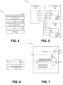
- Figure 4 shows a flow chart of embodiment method 400 for simultaneously writing to a plurality of SPI slaves using the MOSI line, according to an embodiment of the present invention.
- an SPI master connected to an SPI bus sequentially disables the MISO drivers of a set of SPI slaves that are connected to the SPI bus (in other words, turning broadcast mode on).
- the SPI master sequentially disables the MISO drivers of the SPI slaves by writing to a register of each of the SPI slaves using an SPI write command via the MOSI line of the SPI bus.
- the SPI broadcast mode is enabled sequentially issuing SPI write commands to each SPI slave of the set of SPI slaves to write assert an SPI broadcast mode bit.
- the SPI master sets all of the dedicated SS lines of the SPI slave of the set to an active state (to select all the SPI slaves of the set for SPI communication). After all of the SS lines coupled to the set of SPI slaves are set to the active state, the SPI master simultaneously writes (e.g., using a conventional SPI write command) to all the SPI slaves of the set of SPI slaves the same data using the shared MOSI line. Since all the SPI slaves of the set of SPI slaves are selected (have their respective SS pin asserted), all get programmed with the same data.
- any of the registers of the SPI slaves can be simultaneously written in SPI broadcast mode without risking an SPI bus error due to conflict in the MISO line.
- the MISO drivers of the set of SPI slaves are optionally re-enabled.
- the SPI master re-enables all of the MISO drivers via an SPI write command.
- the command to turn broadcast mode off is transmitted simultaneously to all the SPI slaves of the set of SPI slaves using the broadcast mode.
- the SPI broadcast mode is disabled by sequentially writing to each of the SPI slaves of the set to deassert the SPI broadcast mode bit.
- the SPI broadcast mode is disabled automatically at the end the SPI broadcast command.
- the broadcast mode is disabled (the MISO drivers are re-enabled) upon an expiration of a timer (e.g., after a predetermined time has elapsed after the last SPI command transmitted via the SPI bus).
- the broadcast mode may be disabled in other ways, such as by using another pin, or upon an occurrence of an event, such as the toggling of the slave select pin of the SPI slave (e.g., from the active state to the inactive state and back to the active state).
- Advantages of some embodiments include that the bandwidth of the SPI bus is increased as more SPI slaves can be programmed at the same time. Additional advantages include the capability to synchronize multiple SPI slaves using an SPI command (since all the SPI slaves receive the SPI command simultaneously). For example, in some embodiments, multiple devices (e.g., millimeter-wave radars) may be simultaneously enabled using the SPI broadcast mode to perform, e.g., beamforming functions, and other radar functions.
- multiple devices e.g., millimeter-wave radars
- FIG. 5 shows a schematic diagram of system 500, according to an embodiment of the present invention.
- System 500 includes SPI master 102, SPI slaves 504 and 508, and SPI bus 510 coupled to SPI master 102 and to SPI slaves 504 and 508.
- System 500 may be, for example, a millimeter-wave radar system, in which the SPI master 102 is implemented in an application processor (not shown) and SPI slaves 504 and 508 are implemented in two millimeter-wave radars (not shown), respectively.
- System 500 may implement method 400 for simultaneously writing to SPI slaves 504 and 508 using the MOSI line.
- SPI broadcast mode may be enabled in each of SPI slaves 504 and 508 (step 402) by SPI master 102 first asserting SS 504 line and deasserting SS 508 line, issuing an SPI write command to write register 520 of SPI slave 504 via the MOSI line to enable the broadcast mode of SPI slave 504, then asserting SS 508 line and deasserting SS 504 line, and then issuing an SPI write command to write register 520 of SPI slave 508 via the MOSI line to enable the broadcast mode of SPI slave 508.
- Each of the SPI write commands to respective register 520 may be similar to the SPI command shown in Figure 3 .
- SPI master 102 can select both SPI slaves 504 and 508 to be simultaneously programmed (step 404) by asserting both SS 504 and SS 508 lines, and then issuing SPI write commands to program both SPI slaves 504 and 508 simultaneously.
- Figure 6 shows waveforms of the SS 504 , SS 508 , SCLK, MOSI and MISO lines of Figure 5 during an SPI write command by SPI master 102 to SPI slaves 504 and 508 using SPI broadcast mode, according to an embodiment of the present invention.
- the MISO line is in high impedance (HI_Z) since the MISO drivers of each of SPI slaves 504 and 508 are disabled (since the broadcast mode is enabled in each of SPI slaves 504 and 508).
- the MISO line may be pulled low during SPI broadcast mode.
- the MISO line may be pulled high during SPI broadcast mode.
- the MISO line may be left floating during SPI broadcast mode.
- SPI broadcast mode can be disabled (step 406) by issuing an SPI write command to register 520 via the MOSI line. For example, in some embodiments, disabling the SPI broadcast mode takes effect on the next SPI transaction. In such embodiments, the SPI broadcast mode can be disabled by simultaneously writing to all SPI slaves using the SPI broadcast mode.
- Figure 5 illustrates a non-limiting implementation of method 400 with 2 SPI slaves
- some embodiments may implemented method 400 with more than 2 SPI slaves, such as 4, 5, 10, or more.
- the SPI master may enable the SPI broadcast mode on a sub-set of all SPI slaves that are coupled to the SPI bus. For example, in an SPI bus that is coupled to 11 SPI slaves, an SPI master may configure 3 selected SPI slaves in SPI broadcast mode and simultaneously write to the 3 selected SPI slaves while keeping the other SPI slaves unselected (by keeping their respective SS pins deasserted).
- FIG. 7 shows a schematic diagram of a portion of SPI slave 700, according to an embodiment of the present invention.
- SPI slave 700 includes terminal MOSI, MISO, SS, and SCLK, MISO driver 704, MOSI driver 706, multiplexer (MUX) 702, and register bank 710.
- Register bank 710 includes register 520.
- Register 520 (which may be implemented, e.g., with a physical flip-flop per register bit) includes broadcast mode enable bit 720.
- a pull-up resistor (not shown) is coupled to the output of MISO driver 704.
- a pull-down transistor (not shown) is coupled to the output of MISO driver 704.
- MUX 702 couples the SS pin to an enable input of MISO driver 704. Therefore, when SS pin is deasserted (e.g., with a logic 0 in this example), MISO driver 704 is disabled, and when SS pin is asserted (e.g., with a logic 1 in this example), MISO driver 704 is enabled.
- SPI broadcast mode bit 720 each of the SPI write commands to write to any register of register bank 710 may be similar to the SPI command shown in Figure 3 .
- SPI broadcast mode bit 720 When SPI broadcast mode bit 720 is enabled (e.g., with a logic 1 in this example), MUX 702 disables MISO drive 704 irrespective of the state of the SS pin. Therefore, when the SS pin is asserted, SPI slave 700 can receive SPI write commands via the MOSI pin and write any register of register bank 710 while having MISO driver 704 disabled.
- SPI write commands may be similar to the SPI command shown in Figure 6 .
- MISO driver 704 when SPI broadcast mode bit 720 is enabled, MISO driver 704 is disabled even during SPI read commands. In such embodiments, SPI read commands do not transmit data over the MISO line. Therefore, if an SPI master accidentally uses SPI broadcast mode to read from a plurality of SPI slaves, no SPI bus error is generated.
- SPI broadcast mode can be advantageously achieved without redesigning the SPI state machine.
- the SPI state machine (not shown) of the SPI slave is implemented in a conventional manner, thereby generating output data each time an SPI write command is received, irrespective of whether SPI broadcast mode bit is enabled.
- the output data generated is not transmitted to the MISO line because MISO driver 704 is disabled.
- Register bank 710 may be implemented in any way known in the art. It is understand that even though register bank 710 is illustrated in Figure 7 as inside SPI slave 700, in some embodiments, register bank 710 may be implemented outside SPI slave 700.
- the SPI masters and SPI slaves may be implemented in, e.g., integrated circuit, and may be part of devices such as millimeter-wave radars, micro-controllers, processors, or other devices.
- Figure 8 shows a schematic diagram of millimeter-wave radar system 800, according to an embodiment of the present invention.
- Millimeter-wave radar system 800 includes application processor 802, and millimeter-wave radars 804 and 808.
- application processor 802 configures a set of parameters of millimeter-wave radars 804 and 808 via SPI bus 510 using the SPI broadcast mode (e.g., using method 400). For example, in some embodiments, application processor 802 configures, distances between chirps, duration of chirps, and other parameters using the broadcast mode.
- some configuration parameters may be unique to millimeter-wave radar 804, and some configuration parameters may be unique to millimeter-wave radar 808. In such embodiments, such unique configuration parameters may be programmed sequentially using SPI with SPI broadcast mode disabled.
- millimeter-wave radars 804 and 808 may be synchronized by sending a common trigger using SPI broadcast mode.
- Application processor 802 may be implemented as a general purpose processor, controller or digital signal processor (DSP) that includes, for example, combinatorial circuits coupled to a memory.
- application processor 802 may be implemented with an ARM architecture, for example.
- Application processor 802 may be implemented as a custom application specific integrated circuit (ASIC). Other implementations are also possible.
- Millimeter-wave radars 804 and 808 may be implemented in any way known in the art and may operate, for example, as an FMCW radar.
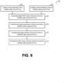
- Figure 9 shows a flow chart of embodiment method 900 for configuring and operating a plurality of millimeter-wave radars using an SPI bus, according to an embodiment of the present invention.
- Method 900 may be implemented, for example, by application processor 902 to configure and operate millimeter-wave radars 804 and 808.
- step 902 parameters that are custom to a first millimeter-wave radar (e.g., millimeter-wave radar 804) are configured using the SPI bus, without SPI broadcast mode. For example, a unique trigger delay assigned to millimeter-wave radar 804 may be programmed during step 902.
- step 904 parameters that are custom to a second millimeter-wave radar (e.g., millimeter-wave radar 808) are configured using the SPI bus (e.g., SPI bus 510), without SPI broadcast mode.
- SPI bus e.g., SPI bus 510
- a unique trigger delay assigned to millimeter-wave radar 808 may be programmed during step 902. If more than 2 millimeter-wave radars are coupled to the SPI bus (e.g., SPI bus 510), similar steps may be performed to configured them.
- step 906 the MISO drivers of each of the plurality of millimeter-wave radars connected to the SPI bus are sequentially disabled in a similar manner as described in step 402.
- steps 902 and 906 may be combined.
- steps 904 and 906 can be combined.
- step 908 all of the millimeter-wave radars coupled to the SPI bus are simultaneously programmed via the SPI bus using the SPI broadcast mode (e.g., in a similar manner as described in step 404) with parameters that are the same for all of the millimeter-wave radars. For example, in some embodiments, parameters such as the distance between chirps, duration of the chirps, frequency of the chirps, etc., are programmed simultaneously in this step. In some embodiments, multiple registers are programmed during this step, thereby advantageously saving programming time.
- step 910 operations of all of the millimeter-wave radars are triggered simultaneously by using the SPI broadcast mode (e.g., in a similar manner as described in step 404). Since each millimeter-wave radar has been programmed with a unique delay for starting operations during steps 902 and 904, transmissions of the chirps may be configured such that the transmission from each of the millimeter-wave radars do not overlap, thereby advantageously allowing, in some embodiments, for time-division multiplexing (TDM) of the plurality of millimeter-wave radars.
- TDM time-division multiplexing
- the SPI broadcast mode may be optionally disabled in a similar manner as described in step 406.
- Advantageous of some embodiments allow for synchronization of multiple devices, such as millimeter-wave radars, without using a dedicated pin of the devices.
Landscapes
- Engineering & Computer Science (AREA)
- Theoretical Computer Science (AREA)
- General Engineering & Computer Science (AREA)
- Physics & Mathematics (AREA)
- General Physics & Mathematics (AREA)
- Software Systems (AREA)
- Computer Hardware Design (AREA)
- Computer Security & Cryptography (AREA)
- Mathematical Physics (AREA)
- Information Transfer Systems (AREA)
Description
- The present disclosure relates generally to an electronic system and method, and, in particular embodiments, to a serial peripheral interface (SPI) broadcast mode.
- There are different communication interfaces that can be used to establish communication between devices. One of these communication interfaces is called SPI.
- Devices implementing SPI can communicate with other devices implementing SPI using a (shared) communication bus that uses a master-slave architecture.
Figure 1 shows exemplary SPImaster 102 and exemplary SPIslave 104 communicating via SPIbus 106. - During normal operation,
SPI master 102 asserts (sets to the active state) the slave select (SS) pin (e.g., with alogic 1 in this case) to select the SPI slave having its SS pin connected to the SS line (in this case SPI slave 104).Master device 102 then generates a SPI clock signal at serial clock (SCLK) pin at a frequency supported bySPI slave 104. - During each SPI clock cycle of data transmission,
SPI master 102 transmits data to the selected SPI slave (in this case SPI slave 104) using the master out slave in (MOSI) pin (connected to the MOSI line) and receives data from the selected SPI slave at the master in slave out (MISO) pin (connected to the MISO line) in synchrony with the SPI clock signal. Correspondingly,SPI slave 104 receives data fromSPI master 102 at the MOSI pin and transmits data toSPI master 102 using the MISO pin in synchrony with the SPI clock signal. -
Figure 2 showsexemplary SPI bus 110 being shared with more than one SPI slave. As show inFigure 2 , the MOSI, MISO, and SCLK lines are shared amongSPI slaves master 102 to select which SPI slave is active for SPI communication to avoid conflicts in the MISO line. - For example, if two SPI slaves (e.g., 104 and 108) are simultaneously transmitting different data (e.g.,
logic 1 and logic 0) in the MISO line, the MISO line will be simultaneously pulled high and low, thereby causing an SPI bus error. To avoid such scenario, when the SS pin of a slave device is deasserted (set to the inactive state -- e.g., with alogic 0 in the example shown inFigures 1 and2), such slave device ignores any data received in its MOSI pin and does not transmit any data with its MISO pin. Therefore, in the example ofFigure 2 , SPImaster 102 can assert SS104 and deassert SS108 to communicate withSPI slave 104, and can assert SS108 and deassert SS104 to communicate withSPI slave 108. - Publication
US 2009/022255 A1 discloses communication to multiple slaves via a SPI Bus. - There is a demand for providing an improved concept for providing a method and a system. Such a demand is satisfied by the subject matter of any of the claims.
- In accordance with an embodiment, a method for writing to a set of SPI slaves coupled to an SPI bus includes: disabling MISO drivers of the set of SPI slaves using the SPI bus; after disabling the MISO drivers, setting respective slave selection terminals of the set of SPI slaves to an active state; and after setting the respective slave selection terminals of the set of SPI slaves to the active state, simultaneously writing data to the set of SPI slaves using a MOSI line.
- In accordance with an embodiment, a system includes an SPI bus, an SPI master, a first SPI slave, and a second SPI slave. The SPI bus includes a MOSI line, and a MISO line. The SPI master incudes a MOSI terminal coupled to the MOSI line, a MISO terminal coupled to the MISO line, a first slave selection terminal, and a second slave selection terminal. The first SPI slave includes a MOSI terminal coupled to the MOSI line, a MISO terminal coupled to the MISO line, a first MISO driver having an output coupled to the MISO terminal of the first SPI slave, and a first slave selection terminal coupled to the first slave selection terminal of the SPI master. The second SPI slave includes a MOSI terminal coupled to the MOSI line, a MISO terminal coupled to the MISO line, a second MISO driver having an output coupled to the MISO terminal of the second SPI slave, and a second slave selection terminal coupled to the second slave selection terminal of the SPI master. The SPI master is configured to: disable the first and second MISO drivers using the SPI bus; after disabling the first and second MISO drivers, set the first and second slave selection terminals of the SPI master to an active state; and after setting the first and second slave selection terminals of the SPI master to an active state, simultaneously write data to the first and second SPI slaves using the MOSI line.
- In accordance with an embodiment, a system includes an SPI bus, an application processor, a first device, and a second device. The SPI bus includes a MOSI line, and a MISO line. The application processor includes an SPI master including a MOSI terminal coupled to the MOSI line, a MISO terminal coupled to the MISO line, a first slave selection terminal, and a second slave selection terminal. The first device has a first register bank and a first SPI slave that includes a MOSI terminal coupled to the MOSI line, a MISO terminal coupled to the MISO line, a first MISO driver having an output coupled to the MISO terminal of the first SPI slave, and a first slave selection terminal coupled to the first slave selection terminal of the SPI master. The second device has a second register bank and a second SPI slave that includes a MOSI terminal coupled to the MOSI line, a MISO terminal coupled to the MISO line, a second MISO driver having an output coupled to the MISO terminal of the second SPI slave, and a second slave selection terminal coupled to the second slave selection terminal of the SPI master. The application processor is configured to: disable the first and second MISO drivers using the SPI master, after disabling the first and second MISO drivers, set the first and second slave selection terminals of the SPI master to an active state, and after setting the first and second slave selection terminals of the SPI master to an active state, simultaneously write data to the first and register banks using via the SPI bus using the SPI master.
- For a more complete understanding of the present invention, and the advantages thereof, reference is now made to the following descriptions taken in conjunction with the accompanying drawings, in which:
-
Figures 1 and 2 show schematic diagrams of exemplary SPI buses between an SPI master and SPI slave devices; -
Figure 3 shows exemplary waveforms of the SS, SCLK, MOSI and MISO lines ofFigure 1 during an exemplary SPI write command by the SPI master ofFigure 1 to the SPI slave ofFigure 1 ; -
Figure 4 shows a flow chart of an embodiment method for simultaneously writing to a plurality of SPI slaves using the MOSI line, according to an embodiment of the present invention; -
Figure 5 shows a schematic diagram of a system, according to an embodiment of the present invention; -
Figure 6 shows waveforms of SS, SCLK, MOSI and MISO lines ofFigure 5 during an SPI write command by the SPI master ofFigure 5 to the SPI slaves ofFigure 5 using SPI broadcast mode, according to an embodiment of the present invention; -
Figure 7 shows a schematic diagram of a portion of an SPI slave, according to an embodiment of the present invention; -
Figure 8 shows a schematic diagram of a millimeter-wave radar system, according to an embodiment of the present invention; and -
Figure 9 shows a flow chart of an embodiment method for configuring and operating a plurality of millimeter-wave radars using an SPI bus, according to an embodiment of the present invention. - Corresponding numerals and symbols in different figures generally refer to corresponding parts unless otherwise indicated. The figures are drawn to clearly illustrate the relevant aspects of the preferred embodiments and are not necessarily drawn to scale.
- The making and using of the embodiments disclosed are discussed in detail below. It should be appreciated, however, that the present invention provides many applicable inventive concepts that can be embodied in a wide variety of specific contexts. The specific embodiments discussed are merely illustrative of specific ways to make and use the invention, and do not limit the scope of the invention.
- The description below illustrates the various specific details to provide an in-depth understanding of several example embodiments according to the description.
- Embodiments of the present invention will be described in a specific context, a broadcast mode for SPI for, e.g., millimeter-wave devices. Embodiments of the present invention may be used in other SPI applications.
- In an embodiment of the present invention, an SPI broadcast mode allows an SPI master to write the same data to a plurality of SPI slave devices simultaneously. In some embodiments, by writing to multiple SPI slaves in parallel, the SPI broadcast mode advantageously allows for faster configuration of multiple SPI slaves without the risk of causing an SPI bus error.
- In conventional SPI communications (such as shown in
Figures 1 and 2 ), every write access (from an SPI master to an SPI slave) is also a read access. In other words, each time SPImaster 102 writes to SPIslave 104 via the MOSI line, SPIslave 104 transmits data to SPImaster 102 via the MISO line. For example,Figure 3 shows exemplary waveforms of the SS, SCLK, MOSI and MISO lines ofFigure 1 during an exemplary SPI write command bySPI master 102 toSPI slave 104. - Therefore, if SPI master 102 (in
Figure 2 ) simultaneously selects SPIslave 104 and SPI slave 108 (e.g., using SS104 and SS108 pins) to write via the MOSI line the same data to both SPI slaves, different content may be written by SPIslaves - Conventionally, SPI bus errors are avoided by SPI
master 102 writingSPI slaves - In an embodiment of the present invention, an SPI master simultaneously writes to a plurality of SPI slaves by configuring the plurality of SPI slaves to operate in SPI broadcast mode using the MOSI line. In SPI broadcast mode, the MISO driver of each of the SPI slaves is disabled. In an embodiment, the SPI master first sequentially configures (e.g., by sequentially asserting the respective SS pin and writing an SPI broadcast bit using an SPI write command via the MOSI line) each of the SPI slaves connected to the SPI bus to operate in SPI broadcast mode. Then, the SPI master asserts all SS pins of the SPI slaves connected to the SPI bus and writes, with all SS pins asserted, to all the SPI slaves in parallel. Optionally, the SPI broadcast mode is then disabled.
-
Figure 4 shows a flow chart ofembodiment method 400 for simultaneously writing to a plurality of SPI slaves using the MOSI line, according to an embodiment of the present invention. - During
step 402, an SPI master connected to an SPI bus sequentially disables the MISO drivers of a set of SPI slaves that are connected to the SPI bus (in other words, turning broadcast mode on). In some embodiments, the SPI master sequentially disables the MISO drivers of the SPI slaves by writing to a register of each of the SPI slaves using an SPI write command via the MOSI line of the SPI bus. For example, in some embodiments, the SPI broadcast mode is enabled sequentially issuing SPI write commands to each SPI slave of the set of SPI slaves to write assert an SPI broadcast mode bit. - During step 404, and after each of the SPI slaves of the set has broadcast mode enabled, the SPI master sets all of the dedicated SS lines of the SPI slave of the set to an active state (to select all the SPI slaves of the set for SPI communication). After all of the SS lines coupled to the set of SPI slaves are set to the active state, the SPI master simultaneously writes (e.g., using a conventional SPI write command) to all the SPI slaves of the set of SPI slaves the same data using the shared MOSI line. Since all the SPI slaves of the set of SPI slaves are selected (have their respective SS pin asserted), all get programmed with the same data. Since broadcast mode is on for all of the SPI slaves of the set (activated during step 402), none of the SPI slaves of the set attempts to transmit data via the MISO line. In some embodiments, any of the registers of the SPI slaves can be simultaneously written in SPI broadcast mode without risking an SPI bus error due to conflict in the MISO line.
- During
step 406, after the SPI slaves of the set have been simultaneously programmed, the MISO drivers of the set of SPI slaves are optionally re-enabled. For example, in some embodiments, the SPI master re-enables all of the MISO drivers via an SPI write command. In some embodiments, the command to turn broadcast mode off is transmitted simultaneously to all the SPI slaves of the set of SPI slaves using the broadcast mode. In some embodiments, the SPI broadcast mode is disabled by sequentially writing to each of the SPI slaves of the set to deassert the SPI broadcast mode bit. In some embodiments, the SPI broadcast mode is disabled automatically at the end the SPI broadcast command. - In some embodiments, the broadcast mode is disabled (the MISO drivers are re-enabled) upon an expiration of a timer (e.g., after a predetermined time has elapsed after the last SPI command transmitted via the SPI bus). The broadcast mode may be disabled in other ways, such as by using another pin, or upon an occurrence of an event, such as the toggling of the slave select pin of the SPI slave (e.g., from the active state to the inactive state and back to the active state).
- Advantages of some embodiments include that the bandwidth of the SPI bus is increased as more SPI slaves can be programmed at the same time. Additional advantages include the capability to synchronize multiple SPI slaves using an SPI command (since all the SPI slaves receive the SPI command simultaneously). For example, in some embodiments, multiple devices (e.g., millimeter-wave radars) may be simultaneously enabled using the SPI broadcast mode to perform, e.g., beamforming functions, and other radar functions.
-
Figure 5 shows a schematic diagram ofsystem 500, according to an embodiment of the present invention.System 500 includesSPI master 102,SPI slaves SPI bus 510 coupled toSPI master 102 and toSPI slaves System 500 may be, for example, a millimeter-wave radar system, in which theSPI master 102 is implemented in an application processor (not shown) andSPI slaves -
System 500 may implementmethod 400 for simultaneously writing toSPI slaves SPI slaves 504 and 508 (step 402) bySPI master 102 first asserting SS504 line and deasserting SS508 line, issuing an SPI write command to writeregister 520 ofSPI slave 504 via the MOSI line to enable the broadcast mode ofSPI slave 504, then asserting SS508 line and deasserting SS504 line, and then issuing an SPI write command to writeregister 520 ofSPI slave 508 via the MOSI line to enable the broadcast mode ofSPI slave 508. Each of the SPI write commands torespective register 520 may be similar to the SPI command shown inFigure 3 . - Once broadcast mode is enabled for both
SPI slaves SPI master 102 can select bothSPI slaves SPI slaves Figure 6 shows waveforms of the SS504, SS508, SCLK, MOSI and MISO lines ofFigure 5 during an SPI write command bySPI master 102 toSPI slaves - As shown in
Figure 6 , during the SPI write command, the MISO line is in high impedance (HI_Z) since the MISO drivers of each ofSPI slaves SPI slaves 504 and 508). In some embodiments, the MISO line may be pulled low during SPI broadcast mode. In other embodiments, the MISO line may be pulled high during SPI broadcast mode. In yet other embodiments, the MISO line may be left floating during SPI broadcast mode. - SPI broadcast mode can be disabled (step 406) by issuing an SPI write command to register 520 via the MOSI line. For example, in some embodiments, disabling the SPI broadcast mode takes effect on the next SPI transaction. In such embodiments, the SPI broadcast mode can be disabled by simultaneously writing to all SPI slaves using the SPI broadcast mode.
- Although
Figure 5 illustrates a non-limiting implementation ofmethod 400 with 2 SPI slaves, it is understood that some embodiments may implementedmethod 400 with more than 2 SPI slaves, such as 4, 5, 10, or more. It is also understood that the SPI master may enable the SPI broadcast mode on a sub-set of all SPI slaves that are coupled to the SPI bus. For example, in an SPI bus that is coupled to 11 SPI slaves, an SPI master may configure 3 selected SPI slaves in SPI broadcast mode and simultaneously write to the 3 selected SPI slaves while keeping the other SPI slaves unselected (by keeping their respective SS pins deasserted). -
Figure 7 shows a schematic diagram of a portion ofSPI slave 700, according to an embodiment of the present invention.SPI slave 700 includes terminal MOSI, MISO, SS, and SCLK,MISO driver 704,MOSI driver 706, multiplexer (MUX) 702, and registerbank 710.Register bank 710 includesregister 520. Register 520 (which may be implemented, e.g., with a physical flip-flop per register bit) includes broadcast mode enablebit 720. In some embodiments, a pull-up resistor (not shown) is coupled to the output ofMISO driver 704. In some embodiments, a pull-down transistor (not shown) is coupled to the output ofMISO driver 704. - During normal operation, when SPI
broadcast mode bit 720 is disabled (e.g., with alogic 0 in this example),MUX 702 couples the SS pin to an enable input ofMISO driver 704. Therefore, when SS pin is deasserted (e.g., with alogic 0 in this example),MISO driver 704 is disabled, and when SS pin is asserted (e.g., with alogic 1 in this example),MISO driver 704 is enabled. When SPIbroadcast mode bit 720 is disabled, each of the SPI write commands to write to any register ofregister bank 710 may be similar to the SPI command shown inFigure 3 . - When SPI
broadcast mode bit 720 is enabled (e.g., with alogic 1 in this example),MUX 702 disables MISO drive 704 irrespective of the state of the SS pin. Therefore, when the SS pin is asserted,SPI slave 700 can receive SPI write commands via the MOSI pin and write any register ofregister bank 710 while havingMISO driver 704 disabled. When SPIbroadcast mode bit 720 is enabled, SPI write commands may be similar to the SPI command shown inFigure 6 . In some embodiments, when SPIbroadcast mode bit 720 is enabled,MISO driver 704 is disabled even during SPI read commands. In such embodiments, SPI read commands do not transmit data over the MISO line. Therefore, if an SPI master accidentally uses SPI broadcast mode to read from a plurality of SPI slaves, no SPI bus error is generated. - In some embodiments, SPI broadcast mode can be advantageously achieved without redesigning the SPI state machine. For example, in some embodiments, the SPI state machine (not shown) of the SPI slave is implemented in a conventional manner, thereby generating output data each time an SPI write command is received, irrespective of whether SPI broadcast mode bit is enabled. However, when the SPI broadcast mode is enabled, the output data generated is not transmitted to the MISO line because
MISO driver 704 is disabled. -
Register bank 710 may be implemented in any way known in the art. It is understand that even thoughregister bank 710 is illustrated inFigure 7 as insideSPI slave 700, in some embodiments,register bank 710 may be implemented outsideSPI slave 700. - The SPI masters and SPI slaves may be implemented in, e.g., integrated circuit, and may be part of devices such as millimeter-wave radars, micro-controllers, processors, or other devices. For example,
Figure 8 shows a schematic diagram of millimeter-wave radar system 800, according to an embodiment of the present invention. Millimeter-wave radar system 800 includesapplication processor 802, and millimeter-wave radars - During normal operation,
application processor 802 configures a set of parameters of millimeter-wave radars SPI bus 510 using the SPI broadcast mode (e.g., using method 400). For example, in some embodiments,application processor 802 configures, distances between chirps, duration of chirps, and other parameters using the broadcast mode. - In some embodiments, some configuration parameters may be unique to millimeter-
wave radar 804, and some configuration parameters may be unique to millimeter-wave radar 808. In such embodiments, such unique configuration parameters may be programmed sequentially using SPI with SPI broadcast mode disabled. - In some embodiments, millimeter-
wave radars -
Application processor 802 may be implemented as a general purpose processor, controller or digital signal processor (DSP) that includes, for example, combinatorial circuits coupled to a memory. In some embodiments,application processor 802 may be implemented with an ARM architecture, for example. In some embodiments,Application processor 802 may be implemented as a custom application specific integrated circuit (ASIC). Other implementations are also possible. - Millimeter-
wave radars -
Figure 9 shows a flow chart ofembodiment method 900 for configuring and operating a plurality of millimeter-wave radars using an SPI bus, according to an embodiment of the present invention.Method 900 may be implemented, for example, byapplication processor 902 to configure and operate millimeter-wave radars - During
step 902, parameters that are custom to a first millimeter-wave radar (e.g., millimeter-wave radar 804) are configured using the SPI bus, without SPI broadcast mode. For example, a unique trigger delay assigned to millimeter-wave radar 804 may be programmed duringstep 902. - During
step 904, parameters that are custom to a second millimeter-wave radar (e.g., millimeter-wave radar 808) are configured using the SPI bus (e.g., SPI bus 510), without SPI broadcast mode. For example, a unique trigger delay assigned to millimeter-wave radar 808 may be programmed duringstep 902. If more than 2 millimeter-wave radars are coupled to the SPI bus (e.g., SPI bus 510), similar steps may be performed to configured them. - During
step 906, the MISO drivers of each of the plurality of millimeter-wave radars connected to the SPI bus are sequentially disabled in a similar manner as described instep 402. In some embodiments,steps steps - During
step 908, all of the millimeter-wave radars coupled to the SPI bus are simultaneously programmed via the SPI bus using the SPI broadcast mode (e.g., in a similar manner as described in step 404) with parameters that are the same for all of the millimeter-wave radars. For example, in some embodiments, parameters such as the distance between chirps, duration of the chirps, frequency of the chirps, etc., are programmed simultaneously in this step. In some embodiments, multiple registers are programmed during this step, thereby advantageously saving programming time. - During
step 910, and after all of the millimeter-wave radars have been custom programmed (step 906) and simultaneously programmed (step 908), operations of all of the millimeter-wave radars are triggered simultaneously by using the SPI broadcast mode (e.g., in a similar manner as described in step 404). Since each millimeter-wave radar has been programmed with a unique delay for starting operations duringsteps - During
step 912, the SPI broadcast mode may be optionally disabled in a similar manner as described instep 406. - Advantageous of some embodiments allow for synchronization of multiple devices, such as millimeter-wave radars, without using a dedicated pin of the devices.
Claims (13)
- A method for writing to a set of serial peripheral interface, SPI, slaves (504, 508) coupled to an SPI bus (510), the method comprising:sequentially writing to each SPI slave of a set of SPI slaves using a MOSI line of the SPI bus to disable master in slave out, MISO, drivers of the set of SPI slaves;after disabling the MISO drivers, setting respective slave selection terminals of the set of SPI slaves to an active state; andafter setting the respective slave selection terminals of the set of SPI slaves to the active state, simultaneously writing data to the set of SPI slaves using a master out slave in, MOSI, line.
- The method of claim 1, further comprising, after simultaneously writing data to the set of SPI slaves, enabling the MISO drivers of the set of SPI slaves.
- The method of claim 1 or 2, wherein enabling the MISO drivers of the set of SPI slaves comprises enabling the MISO drivers of the set of SPI slaves by writing data to the set of SPI slaves using the MOSI line.
- The method of claim 2 or 3, wherein enabling the MISO drivers of the set of SPI slaves comprises enabling the MISO drivers of the set of SPI slaves by toggling the respective slave selection lines of the set of SPI slaves to an inactive state and then to the active state.
- The method of any of claims 2 to 4, wherein enabling the MISO drivers of the set of SPI slaves comprises enabling the MISO drivers of the set of SPI slaves when a respective timer of each of the set of SPI slaves expires.
- The method of claim any one of claims 1 to 5, wherein each respective SPI slave of the set of SPI slaves transmits data via the MISO line during the disabling of the respective MISO driver of the respective SPI slave.
- The method of any of the preceding claims, wherein disabling the MISO drivers of the set of SPI slaves comprises setting respective SPI broadcast mode bits of each respective SPI slave of the set of SPI slaves to an active state.
- The method of claim 7, wherein each respective SPI slave of the set of SPI slaves comprises a selection circuit that disables the respective MISO driver when the respective SPI broadcast mode bit is in the active state.
- The method of claim 8, wherein the selection circuit is a multiplexer that couples the respective slave selection terminal to an enable terminal of the respective MISO driver when the respective SPI broadcast mode bit is in an active state.
- A system comprising:a serial peripheral interface, SPI, bus (510) comprising a master out slave in, MOSI, line, and a master in slave out, MISO, line;an SPI master (102) comprising a MOSI terminal coupled to the MOSI line, a MISO terminal coupled to the MISO line, a first slave selection terminal, and a second slave selection terminal;a first SPI slave (504) comprising a MOSI terminal coupled to the MOSI line, a MISO terminal coupled to the MISO line, a first MISO driver having an output coupled to the MISO terminal of the first SPI slave, and a first slave selection terminal coupled to the first slave selection terminal of the SPI master; anda second SPI slave (508) comprising a MOSI terminal coupled to the MOSI line, a MISO terminal coupled to the MISO line, a second MISO driver having an output coupled to the MISO terminal of the second SPI slave, and a second slave selection terminal coupled to the second slave selection terminal of the SPI master, wherein the SPI master is configured to:disable the first and second MISO drivers by sequentially writing to the first SPI slave and the second SPI slave using the MOSI line of the SPI bus to;after disabling the first and second MISO drivers, set the first and second slave selection terminals of the SPI master to an active state; andafter setting the first and second slave selection terminals of the SPI master to an active state, simultaneously write data to the first and second SPI slaves using the MOSI line.
- The system of claim 10, wherein the SPI master is further configured to enable the first and second MISO driver s after simultaneously writing data to the first and second SPI slaves.
- The system of claim 11, wherein the SPI master is configured to enable the first and second MISO drivers by using the SPI bus.
- The system of any of claims 10 to 12, wherein the first MISO driver comprises a first enable terminal, wherein the second MISO driver comprises a second enable terminal, wherein the first SPI slave further comprises a first SPI broadcast bit and a first selection circuit configured to control the first enable terminal based on the first SPI broadcast bit, and wherein the second SPI slave further comprises a second SPI broadcast bit and a second selection circuit configured to control the second enable terminal based on the second SPI broadcast bit.
Applications Claiming Priority (1)
| Application Number | Priority Date | Filing Date | Title |
|---|---|---|---|
| US16/779,126 US11188495B2 (en) | 2020-01-31 | 2020-01-31 | SPI broadcast mode |
Publications (2)
| Publication Number | Publication Date |
|---|---|
| EP3859542A1 EP3859542A1 (en) | 2021-08-04 |
| EP3859542B1 true EP3859542B1 (en) | 2023-05-10 |
Family
ID=74418287
Family Applications (1)
| Application Number | Title | Priority Date | Filing Date |
|---|---|---|---|
| EP21154320.2A Active EP3859542B1 (en) | 2020-01-31 | 2021-01-29 | Spi broadcast mode |
Country Status (3)
| Country | Link |
|---|---|
| US (1) | US11188495B2 (en) |
| EP (1) | EP3859542B1 (en) |
| CN (1) | CN113282528A (en) |
Families Citing this family (8)
| Publication number | Priority date | Publication date | Assignee | Title |
|---|---|---|---|---|
| CN113407478B (en) * | 2021-08-23 | 2021-11-30 | 上海泰矽微电子有限公司 | Method for realizing active application transmission of SPI slave equipment |
| US11847087B2 (en) * | 2021-09-16 | 2023-12-19 | Qualcomm Incorporated | Systems and methods for chip operation using serial peripheral interface (SPI) with reduced pin options |
| CN114528235B (en) * | 2022-01-21 | 2024-05-31 | 厦门亿联网络技术股份有限公司 | SPI-based communication method, slave device and system |
| CN115033517B (en) * | 2022-05-30 | 2023-12-19 | 浙江大学 | Device for realizing multi-line SPI interface transmission based on multiple single-line SPI interfaces |
| US11841994B1 (en) * | 2022-06-02 | 2023-12-12 | Pixart Imaging Inc. | Optical navigation system and optical sensor control method |
| EP4609296A1 (en) * | 2022-10-27 | 2025-09-03 | Kandou Labs SA | Firmware broadcast in a multi-chip module |
| CN116578513A (en) * | 2023-03-31 | 2023-08-11 | 上海矽力杰微电子技术有限公司 | Communication system and communication method |
| US20260195287A1 (en) * | 2025-01-03 | 2026-07-09 | Renesas Electronics Corporation | Addressable serial peripheral interface |
Family Cites Families (12)
| Publication number | Priority date | Publication date | Assignee | Title |
|---|---|---|---|---|
| US6931470B2 (en) * | 2002-02-11 | 2005-08-16 | Motorola, Inc. | Dual access serial peripheral interface |
| JP4141373B2 (en) | 2003-11-05 | 2008-08-27 | 株式会社日立製作所 | COMMUNICATION SYSTEM, REAL TIME CONTROL DEVICE AND INFORMATION PROCESSING SYSTEM |
| US7761633B2 (en) * | 2007-01-29 | 2010-07-20 | Microsemi Corp. - Analog Mixed Signal Group Ltd. | Addressable serial peripheral interface |
| US10684974B1 (en) * | 2007-03-12 | 2020-06-16 | Cypress Semiconductor Corporation | Auto-switching communication interface |
| US8433838B2 (en) * | 2010-09-17 | 2013-04-30 | International Business Machines Corporation | Remote multiplexing devices on a serial peripheral interface bus |
| KR20120055034A (en) * | 2010-11-22 | 2012-05-31 | 삼성전자주식회사 | Apparatus for connecting peripheral device in portable terminal using serial peripheral interface and method for transmitting data |
| US8892933B2 (en) * | 2012-04-23 | 2014-11-18 | Analog Devices, Inc. | Synchronization of multiple signal converters by transmitting signal conversion data and receiving unique correction values for the respective counters through the same data interface pins |
| US10061016B2 (en) * | 2014-12-29 | 2018-08-28 | Texas Instruments Incorporated | Phase noise measurement in a cascaded radar system |
| US9990316B2 (en) * | 2015-09-21 | 2018-06-05 | Qualcomm Incorporated | Enhanced serial peripheral interface |
| US10235324B2 (en) * | 2015-09-30 | 2019-03-19 | Nxp Usa, Inc. | Interconnect sharing with integrated control for reduced pinout |
| US9734099B1 (en) * | 2017-04-27 | 2017-08-15 | Micro Lambda Wireless, Inc. | QSPI based methods of simultaneously controlling multiple SPI peripherals |
| US11188492B2 (en) * | 2018-12-27 | 2021-11-30 | Intel Corporation | Enhanced serial peripheral interface (eSPI) port expander |
-
2020
- 2020-01-31 US US16/779,126 patent/US11188495B2/en active Active
-
2021
- 2021-01-29 CN CN202110126015.2A patent/CN113282528A/en active Pending
- 2021-01-29 EP EP21154320.2A patent/EP3859542B1/en active Active
Also Published As
| Publication number | Publication date |
|---|---|
| CN113282528A (en) | 2021-08-20 |
| US20210240656A1 (en) | 2021-08-05 |
| US11188495B2 (en) | 2021-11-30 |
| EP3859542A1 (en) | 2021-08-04 |
Similar Documents
| Publication | Publication Date | Title |
|---|---|---|
| US11188495B2 (en) | SPI broadcast mode | |
| US9274997B2 (en) | Point-to-point serial peripheral interface for data communication between devices configured in a daisy-chain | |
| JP2018506232A (en) | Receive clock calibration for serial bus | |
| US20100064083A1 (en) | Communications device without passive pullup components | |
| TW201411482A (en) | Ring topology status indication | |
| US20220188254A1 (en) | Methods for identifying target slave address for serial communication interface | |
| US7529273B2 (en) | Method and system for synchronizing communications links in a hub-based memory system | |
| JPH0784863A (en) | Information processing apparatus and semiconductor memory device suitable for the same | |
| WO2007124304A2 (en) | Serial communications bus with active pullup | |
| US9202541B2 (en) | Semiconductor apparatus configured to reduce data processing performance | |
| US7852687B2 (en) | Low power shift register and semiconductor memory device including the same | |
| CN114996184A (en) | Compatible implementation of SPI or I 2 Interface module of C slave machine and data transmission method | |
| CN114911743B (en) | SPI slave device, SPI master device and related communication method | |
| US7461187B2 (en) | Bus system and data transfer method | |
| US11947478B2 (en) | Methods for identifying target slave address for serial communication interface | |
| US20050060458A1 (en) | Method and apparatus for sharing a device among multiple CPU systems | |
| US20130086334A1 (en) | Serially connected memory having subdivided data interface | |
| CN117370258B (en) | Multipath low-speed I2C expansion method and device for high-speed I2C bus | |
| US6052746A (en) | Integrated circuit having programmable pull device configured to enable/disable first function in favor of second function according to predetermined scheme before/after reset | |
| CN101160569A (en) | Device for improving the bandwidth of a circuit with multiple memory controllers | |
| US9367495B1 (en) | High speed integrated circuit interface | |
| CN114546931B (en) | FPGA-based multi-signal selection method, system, electronic device, and storage medium | |
| US7068727B1 (en) | Halting data strobes on a source synchronous link and utilization of same to debug data capture problems | |
| US20180181511A1 (en) | Dynamic termination circuit, semiconductor apparatus and system including the same | |
| US20030053573A1 (en) | Microcontroller having a transmission-bus-interface |
Legal Events
| Date | Code | Title | Description |
|---|---|---|---|
| PUAI | Public reference made under article 153(3) epc to a published international application that has entered the european phase |
Free format text: ORIGINAL CODE: 0009012 |
|
| STAA | Information on the status of an ep patent application or granted ep patent |
Free format text: STATUS: THE APPLICATION HAS BEEN PUBLISHED |
|
| AK | Designated contracting states |
Kind code of ref document: A1 Designated state(s): AL AT BE BG CH CY CZ DE DK EE ES FI FR GB GR HR HU IE IS IT LI LT LU LV MC MK MT NL NO PL PT RO RS SE SI SK SM TR |
|
| STAA | Information on the status of an ep patent application or granted ep patent |
Free format text: STATUS: REQUEST FOR EXAMINATION WAS MADE |
|
| 17P | Request for examination filed |
Effective date: 20220131 |
|
| RBV | Designated contracting states (corrected) |
Designated state(s): AL AT BE BG CH CY CZ DE DK EE ES FI FR GB GR HR HU IE IS IT LI LT LU LV MC MK MT NL NO PL PT RO RS SE SI SK SM TR |
|
| GRAP | Despatch of communication of intention to grant a patent |
Free format text: ORIGINAL CODE: EPIDOSNIGR1 |
|
| STAA | Information on the status of an ep patent application or granted ep patent |
Free format text: STATUS: GRANT OF PATENT IS INTENDED |
|
| INTG | Intention to grant announced |
Effective date: 20230201 |
|
| GRAS | Grant fee paid |
Free format text: ORIGINAL CODE: EPIDOSNIGR3 |
|
| GRAA | (expected) grant |
Free format text: ORIGINAL CODE: 0009210 |
|
| STAA | Information on the status of an ep patent application or granted ep patent |
Free format text: STATUS: THE PATENT HAS BEEN GRANTED |
|
| AK | Designated contracting states |
Kind code of ref document: B1 Designated state(s): AL AT BE BG CH CY CZ DE DK EE ES FI FR GB GR HR HU IE IS IT LI LT LU LV MC MK MT NL NO PL PT RO RS SE SI SK SM TR |
|
| REG | Reference to a national code |
Ref country code: GB Ref legal event code: FG4D |
|
| REG | Reference to a national code |
Ref country code: AT Ref legal event code: REF Ref document number: 1567403 Country of ref document: AT Kind code of ref document: T Effective date: 20230515 Ref country code: CH Ref legal event code: EP |
|
| REG | Reference to a national code |
Ref country code: DE Ref legal event code: R096 Ref document number: 602021002216 Country of ref document: DE |
|
| REG | Reference to a national code |
Ref country code: IE Ref legal event code: FG4D |
|
| REG | Reference to a national code |
Ref country code: LT Ref legal event code: MG9D |
|
| P01 | Opt-out of the competence of the unified patent court (upc) registered |
Effective date: 20230804 |
|
| REG | Reference to a national code |
Ref country code: NL Ref legal event code: MP Effective date: 20230510 |
|
| REG | Reference to a national code |
Ref country code: AT Ref legal event code: MK05 Ref document number: 1567403 Country of ref document: AT Kind code of ref document: T Effective date: 20230510 |
|
| PG25 | Lapsed in a contracting state [announced via postgrant information from national office to epo] |
Ref country code: SE Free format text: LAPSE BECAUSE OF FAILURE TO SUBMIT A TRANSLATION OF THE DESCRIPTION OR TO PAY THE FEE WITHIN THE PRESCRIBED TIME-LIMIT Effective date: 20230510 Ref country code: PT Free format text: LAPSE BECAUSE OF FAILURE TO SUBMIT A TRANSLATION OF THE DESCRIPTION OR TO PAY THE FEE WITHIN THE PRESCRIBED TIME-LIMIT Effective date: 20230911 Ref country code: NO Free format text: LAPSE BECAUSE OF FAILURE TO SUBMIT A TRANSLATION OF THE DESCRIPTION OR TO PAY THE FEE WITHIN THE PRESCRIBED TIME-LIMIT Effective date: 20230810 Ref country code: NL Free format text: LAPSE BECAUSE OF FAILURE TO SUBMIT A TRANSLATION OF THE DESCRIPTION OR TO PAY THE FEE WITHIN THE PRESCRIBED TIME-LIMIT Effective date: 20230510 Ref country code: ES Free format text: LAPSE BECAUSE OF FAILURE TO SUBMIT A TRANSLATION OF THE DESCRIPTION OR TO PAY THE FEE WITHIN THE PRESCRIBED TIME-LIMIT Effective date: 20230510 Ref country code: AT Free format text: LAPSE BECAUSE OF FAILURE TO SUBMIT A TRANSLATION OF THE DESCRIPTION OR TO PAY THE FEE WITHIN THE PRESCRIBED TIME-LIMIT Effective date: 20230510 |
|
| PG25 | Lapsed in a contracting state [announced via postgrant information from national office to epo] |
Ref country code: RS Free format text: LAPSE BECAUSE OF FAILURE TO SUBMIT A TRANSLATION OF THE DESCRIPTION OR TO PAY THE FEE WITHIN THE PRESCRIBED TIME-LIMIT Effective date: 20230510 Ref country code: PL Free format text: LAPSE BECAUSE OF FAILURE TO SUBMIT A TRANSLATION OF THE DESCRIPTION OR TO PAY THE FEE WITHIN THE PRESCRIBED TIME-LIMIT Effective date: 20230510 Ref country code: LV Free format text: LAPSE BECAUSE OF FAILURE TO SUBMIT A TRANSLATION OF THE DESCRIPTION OR TO PAY THE FEE WITHIN THE PRESCRIBED TIME-LIMIT Effective date: 20230510 Ref country code: LT Free format text: LAPSE BECAUSE OF FAILURE TO SUBMIT A TRANSLATION OF THE DESCRIPTION OR TO PAY THE FEE WITHIN THE PRESCRIBED TIME-LIMIT Effective date: 20230510 Ref country code: IS Free format text: LAPSE BECAUSE OF FAILURE TO SUBMIT A TRANSLATION OF THE DESCRIPTION OR TO PAY THE FEE WITHIN THE PRESCRIBED TIME-LIMIT Effective date: 20230910 Ref country code: HR Free format text: LAPSE BECAUSE OF FAILURE TO SUBMIT A TRANSLATION OF THE DESCRIPTION OR TO PAY THE FEE WITHIN THE PRESCRIBED TIME-LIMIT Effective date: 20230510 Ref country code: GR Free format text: LAPSE BECAUSE OF FAILURE TO SUBMIT A TRANSLATION OF THE DESCRIPTION OR TO PAY THE FEE WITHIN THE PRESCRIBED TIME-LIMIT Effective date: 20230811 |
|
| PG25 | Lapsed in a contracting state [announced via postgrant information from national office to epo] |
Ref country code: FI Free format text: LAPSE BECAUSE OF FAILURE TO SUBMIT A TRANSLATION OF THE DESCRIPTION OR TO PAY THE FEE WITHIN THE PRESCRIBED TIME-LIMIT Effective date: 20230510 |
|
| PG25 | Lapsed in a contracting state [announced via postgrant information from national office to epo] |
Ref country code: SK Free format text: LAPSE BECAUSE OF FAILURE TO SUBMIT A TRANSLATION OF THE DESCRIPTION OR TO PAY THE FEE WITHIN THE PRESCRIBED TIME-LIMIT Effective date: 20230510 |
|
| PG25 | Lapsed in a contracting state [announced via postgrant information from national office to epo] |
Ref country code: SM Free format text: LAPSE BECAUSE OF FAILURE TO SUBMIT A TRANSLATION OF THE DESCRIPTION OR TO PAY THE FEE WITHIN THE PRESCRIBED TIME-LIMIT Effective date: 20230510 Ref country code: SK Free format text: LAPSE BECAUSE OF FAILURE TO SUBMIT A TRANSLATION OF THE DESCRIPTION OR TO PAY THE FEE WITHIN THE PRESCRIBED TIME-LIMIT Effective date: 20230510 Ref country code: RO Free format text: LAPSE BECAUSE OF FAILURE TO SUBMIT A TRANSLATION OF THE DESCRIPTION OR TO PAY THE FEE WITHIN THE PRESCRIBED TIME-LIMIT Effective date: 20230510 Ref country code: EE Free format text: LAPSE BECAUSE OF FAILURE TO SUBMIT A TRANSLATION OF THE DESCRIPTION OR TO PAY THE FEE WITHIN THE PRESCRIBED TIME-LIMIT Effective date: 20230510 Ref country code: DK Free format text: LAPSE BECAUSE OF FAILURE TO SUBMIT A TRANSLATION OF THE DESCRIPTION OR TO PAY THE FEE WITHIN THE PRESCRIBED TIME-LIMIT Effective date: 20230510 Ref country code: CZ Free format text: LAPSE BECAUSE OF FAILURE TO SUBMIT A TRANSLATION OF THE DESCRIPTION OR TO PAY THE FEE WITHIN THE PRESCRIBED TIME-LIMIT Effective date: 20230510 |
|
| REG | Reference to a national code |
Ref country code: DE Ref legal event code: R097 Ref document number: 602021002216 Country of ref document: DE |
|
| PLBE | No opposition filed within time limit |
Free format text: ORIGINAL CODE: 0009261 |
|
| STAA | Information on the status of an ep patent application or granted ep patent |
Free format text: STATUS: NO OPPOSITION FILED WITHIN TIME LIMIT |
|
| 26N | No opposition filed |
Effective date: 20240213 |
|
| PG25 | Lapsed in a contracting state [announced via postgrant information from national office to epo] |
Ref country code: SI Free format text: LAPSE BECAUSE OF FAILURE TO SUBMIT A TRANSLATION OF THE DESCRIPTION OR TO PAY THE FEE WITHIN THE PRESCRIBED TIME-LIMIT Effective date: 20230510 |
|
| PG25 | Lapsed in a contracting state [announced via postgrant information from national office to epo] |
Ref country code: SI Free format text: LAPSE BECAUSE OF FAILURE TO SUBMIT A TRANSLATION OF THE DESCRIPTION OR TO PAY THE FEE WITHIN THE PRESCRIBED TIME-LIMIT Effective date: 20230510 Ref country code: IT Free format text: LAPSE BECAUSE OF FAILURE TO SUBMIT A TRANSLATION OF THE DESCRIPTION OR TO PAY THE FEE WITHIN THE PRESCRIBED TIME-LIMIT Effective date: 20230510 |
|
| PG25 | Lapsed in a contracting state [announced via postgrant information from national office to epo] |
Ref country code: MC Free format text: LAPSE BECAUSE OF FAILURE TO SUBMIT A TRANSLATION OF THE DESCRIPTION OR TO PAY THE FEE WITHIN THE PRESCRIBED TIME-LIMIT Effective date: 20230510 |
|
| PG25 | Lapsed in a contracting state [announced via postgrant information from national office to epo] |
Ref country code: MC Free format text: LAPSE BECAUSE OF FAILURE TO SUBMIT A TRANSLATION OF THE DESCRIPTION OR TO PAY THE FEE WITHIN THE PRESCRIBED TIME-LIMIT Effective date: 20230510 |
|
| REG | Reference to a national code |
Ref country code: CH Ref legal event code: PL |
|
| PG25 | Lapsed in a contracting state [announced via postgrant information from national office to epo] |
Ref country code: LU Free format text: LAPSE BECAUSE OF NON-PAYMENT OF DUE FEES Effective date: 20240129 |
|
| PG25 | Lapsed in a contracting state [announced via postgrant information from national office to epo] |
Ref country code: LU Free format text: LAPSE BECAUSE OF NON-PAYMENT OF DUE FEES Effective date: 20240129 |
|
| PG25 | Lapsed in a contracting state [announced via postgrant information from national office to epo] |
Ref country code: BE Free format text: LAPSE BECAUSE OF NON-PAYMENT OF DUE FEES Effective date: 20240131 |
|
| PG25 | Lapsed in a contracting state [announced via postgrant information from national office to epo] |
Ref country code: CH Free format text: LAPSE BECAUSE OF NON-PAYMENT OF DUE FEES Effective date: 20240131 |
|
| PG25 | Lapsed in a contracting state [announced via postgrant information from national office to epo] |
Ref country code: CH Free format text: LAPSE BECAUSE OF NON-PAYMENT OF DUE FEES Effective date: 20240131 Ref country code: BE Free format text: LAPSE BECAUSE OF NON-PAYMENT OF DUE FEES Effective date: 20240131 |
|
| REG | Reference to a national code |
Ref country code: BE Ref legal event code: MM Effective date: 20240131 |
|
| PG25 | Lapsed in a contracting state [announced via postgrant information from national office to epo] |
Ref country code: BG Free format text: LAPSE BECAUSE OF FAILURE TO SUBMIT A TRANSLATION OF THE DESCRIPTION OR TO PAY THE FEE WITHIN THE PRESCRIBED TIME-LIMIT Effective date: 20230510 |
|
| PG25 | Lapsed in a contracting state [announced via postgrant information from national office to epo] |
Ref country code: BG Free format text: LAPSE BECAUSE OF FAILURE TO SUBMIT A TRANSLATION OF THE DESCRIPTION OR TO PAY THE FEE WITHIN THE PRESCRIBED TIME-LIMIT Effective date: 20230510 |
|
| PG25 | Lapsed in a contracting state [announced via postgrant information from national office to epo] |
Ref country code: IE Free format text: LAPSE BECAUSE OF NON-PAYMENT OF DUE FEES Effective date: 20240129 |
|
| PG25 | Lapsed in a contracting state [announced via postgrant information from national office to epo] |
Ref country code: IE Free format text: LAPSE BECAUSE OF NON-PAYMENT OF DUE FEES Effective date: 20240129 |
|
| PG25 | Lapsed in a contracting state [announced via postgrant information from national office to epo] |
Ref country code: CY Free format text: LAPSE BECAUSE OF FAILURE TO SUBMIT A TRANSLATION OF THE DESCRIPTION OR TO PAY THE FEE WITHIN THE PRESCRIBED TIME-LIMIT; INVALID AB INITIO Effective date: 20210129 |
|
| PG25 | Lapsed in a contracting state [announced via postgrant information from national office to epo] |
Ref country code: HU Free format text: LAPSE BECAUSE OF FAILURE TO SUBMIT A TRANSLATION OF THE DESCRIPTION OR TO PAY THE FEE WITHIN THE PRESCRIBED TIME-LIMIT; INVALID AB INITIO Effective date: 20210129 |
|
| PG25 | Lapsed in a contracting state [announced via postgrant information from national office to epo] |
Ref country code: TR Free format text: LAPSE BECAUSE OF FAILURE TO SUBMIT A TRANSLATION OF THE DESCRIPTION OR TO PAY THE FEE WITHIN THE PRESCRIBED TIME-LIMIT Effective date: 20230510 |
|
| PGFP | Annual fee paid to national office [announced via postgrant information from national office to epo] |
Ref country code: GB Payment date: 20260123 Year of fee payment: 6 |
|
| PGFP | Annual fee paid to national office [announced via postgrant information from national office to epo] |
Ref country code: DE Payment date: 20260323 Year of fee payment: 6 |
|
| PGFP | Annual fee paid to national office [announced via postgrant information from national office to epo] |
Ref country code: FR Payment date: 20260123 Year of fee payment: 6 |