EP3859534A1 - Data deduplication - Google Patents
Data deduplication Download PDFInfo
- Publication number
- EP3859534A1 EP3859534A1 EP21164611.2A EP21164611A EP3859534A1 EP 3859534 A1 EP3859534 A1 EP 3859534A1 EP 21164611 A EP21164611 A EP 21164611A EP 3859534 A1 EP3859534 A1 EP 3859534A1
- Authority
- EP
- European Patent Office
- Prior art keywords
- data
- transformation
- hash
- memory device
- values
- Prior art date
- Legal status (The legal status is an assumption and is not a legal conclusion. Google has not performed a legal analysis and makes no representation as to the accuracy of the status listed.)
- Pending
Links
Images

Classifications
-
- G—PHYSICS
- G06—COMPUTING OR CALCULATING; COUNTING
- G06F—ELECTRIC DIGITAL DATA PROCESSING
- G06F3/00—Input arrangements for transferring data to be processed into a form capable of being handled by the computer; Output arrangements for transferring data from processing unit to output unit, e.g. interface arrangements
- G06F3/06—Digital input from, or digital output to, record carriers, e.g. RAID, emulated record carriers or networked record carriers
- G06F3/0601—Interfaces specially adapted for storage systems
- G06F3/0628—Interfaces specially adapted for storage systems making use of a particular technique
- G06F3/0638—Organizing or formatting or addressing of data
- G06F3/064—Management of blocks
- G06F3/0641—De-duplication techniques
-
- G—PHYSICS
- G06—COMPUTING OR CALCULATING; COUNTING
- G06F—ELECTRIC DIGITAL DATA PROCESSING
- G06F11/00—Error detection; Error correction; Monitoring
- G06F11/07—Responding to the occurrence of a fault, e.g. fault tolerance
- G06F11/08—Error detection or correction by redundancy in data representation, e.g. by using checking codes
-
- G—PHYSICS
- G06—COMPUTING OR CALCULATING; COUNTING
- G06F—ELECTRIC DIGITAL DATA PROCESSING
- G06F12/00—Accessing, addressing or allocating within memory systems or architectures
-
- G—PHYSICS
- G06—COMPUTING OR CALCULATING; COUNTING
- G06F—ELECTRIC DIGITAL DATA PROCESSING
- G06F12/00—Accessing, addressing or allocating within memory systems or architectures
- G06F12/02—Addressing or allocation; Relocation
- G06F12/0223—User address space allocation, e.g. contiguous or non contiguous base addressing
- G06F12/023—Free address space management
-
- G—PHYSICS
- G06—COMPUTING OR CALCULATING; COUNTING
- G06F—ELECTRIC DIGITAL DATA PROCESSING
- G06F3/00—Input arrangements for transferring data to be processed into a form capable of being handled by the computer; Output arrangements for transferring data from processing unit to output unit, e.g. interface arrangements
- G06F3/06—Digital input from, or digital output to, record carriers, e.g. RAID, emulated record carriers or networked record carriers
- G06F3/0601—Interfaces specially adapted for storage systems
- G06F3/0602—Interfaces specially adapted for storage systems specifically adapted to achieve a particular effect
- G06F3/0608—Saving storage space on storage systems
-
- G—PHYSICS
- G06—COMPUTING OR CALCULATING; COUNTING
- G06F—ELECTRIC DIGITAL DATA PROCESSING
- G06F3/00—Input arrangements for transferring data to be processed into a form capable of being handled by the computer; Output arrangements for transferring data from processing unit to output unit, e.g. interface arrangements
- G06F3/06—Digital input from, or digital output to, record carriers, e.g. RAID, emulated record carriers or networked record carriers
- G06F3/0601—Interfaces specially adapted for storage systems
- G06F3/0668—Interfaces specially adapted for storage systems adopting a particular infrastructure
- G06F3/0671—In-line storage system
- G06F3/0673—Single storage device
-
- G—PHYSICS
- G06—COMPUTING OR CALCULATING; COUNTING
- G06F—ELECTRIC DIGITAL DATA PROCESSING
- G06F3/00—Input arrangements for transferring data to be processed into a form capable of being handled by the computer; Output arrangements for transferring data from processing unit to output unit, e.g. interface arrangements
- G06F3/06—Digital input from, or digital output to, record carriers, e.g. RAID, emulated record carriers or networked record carriers
- G06F3/0601—Interfaces specially adapted for storage systems
- G06F3/0668—Interfaces specially adapted for storage systems adopting a particular infrastructure
- G06F3/0671—In-line storage system
- G06F3/0673—Single storage device
- G06F3/0679—Non-volatile semiconductor memory device, e.g. flash memory, one time programmable memory [OTP]
Definitions
- the present disclosure relates generally to semiconductor memory devices and methods, and more particularly, to devices and methods for data deduplication.
- RAM random-access memory
- ROM read only memory
- DRAM dynamic random access memory
- SDRAM synchronous dynamic random access memory
- PCRAM phase change random access memory
- flash memory among others.
- Non-volatile memory Memory devices are utilized as non-volatile memory for a wide range of electronic applications in need of high memory densities, high reliability, and low power consumption.
- Non-volatile memory may be used in a personal computer, a portable memory stick, a solid state drive (SSD), a personal digital assistant (PDA), a digital camera, a cellular telephone, a portable music player e.g., MP3 player, a movie player, and other electronic devices, among others.
- Data such as program code, and system data, such as a basic input/output system (BIOS), are typically stored in non-volatile memory devices.
- BIOS basic input/output system
- Memory systems can receive write commands from a host, with the write commands being associated with, e.g., including, data to be written to one or more memory devices of the memory system.
- the data associated with, e.g., in, a write command can include a number of portions, e.g., sectors, with each portion having a unique logical address associated therewith.
- Each logical address can be assigned a physical address associated with a physical location, and each portion of data in a write command can be written to a particular physical location associated with the physical address assigned to the logical address corresponding to each portion of the data.
- different logical addresses can correspond to the same physical data such that the data is physically duplicated in one or more memory devices of the memory system. Writing duplicate data can unnecessarily decrease the storage capacity of a memory system, among other drawbacks.
- the present disclosure includes devices and methods for data deduplication.
- One such method includes receiving a write command, transforming data associated with, e.g., from, the write command, determining if a transformation value of the data exists in a transformation table, and responsive to a determination that the transformation value does not exist in the transformation table, writing the data associated with the write command to a memory device.
- Data deduplication can include avoiding writing duplicate data to a memory system.
- a host would compare files to be written to a memory system with the files on the memory system to determine if a file is already present on the memory system and delete existing duplicate files present on the memory system. In such approaches, if a file was present on the memory system, the host would not send the command to write that file to the memory system, thus avoiding duplication of the file on the memory system.
- data deduplication can include transforming, e.g., hashing, each sector of data that is received by a memory system from a host.
- the hashing of each sector of data can include generating a transformation value, e.g., hash value, for each sector of data received in a write command.
- a transformation value e.g., hash value
- Embodiments are not limited to hashing each sector of data and data can be hashed in any increment, such as pages, for example.
- the hash values generated for each sector of data can be compared to hash values in a transformation table, e.g., hash table, for data that is currently written to memory devices in a memory system. If a hash value generated for a sector of data received in a write command does not exist, e.g., is not present, in the hash table, the sector of data is written to a location in the memory devices and the hash table is updated by writing an entry to the hash table that includes the hash value of the sector data.
- the hash table can also be updated by writing an entry to the hash table that includes a logical address of the sector of data and a physical address of the sector of data.
- the hash table is updated by writing an entry to the hash table to associate the logical address of the sector of data with the hash value of the sector data.
- a successful write indication can be sent to the host when the hash table is updated with the hash value and a logical address and physical address of the sector of data.
- a number of something can refer to one or more such things.
- a number of memory devices can refer to one or more memory devices.
- the designators "N" and “M” as used herein, particularly with respect to reference numerals in the drawings, indicates that a number of the particular feature so designated can be included with a number of embodiments of the present disclosure.
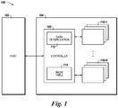
- FIG. 1 is a functional block diagram of a computing device 100 including at least one memory system 104, in accordance with one or more embodiments of the present disclosure.
- the memory system 104 can include a controller 108 and one or more memory devices 110-1, ..., 110-N.
- the controller 108 is external to the one or more memory devices 110-1, ..., 110-N.
- the memory devices 110-1, .. ., 110-N can provide a storage volume for the memory system, e.g., with a file system formatted to the memory devices.
- the controller 108 can include control circuitry, e.g., hardware, firmware, and/or software.
- the controller 108 can be an application specific integrated circuit (ASIC) coupled to a printed circuit board including a physical interface and memory devices 110-1, ..., 110-N.
- ASIC application specific integrated circuit
- the controller 108 can include a data deduplication component 112 and a hash table 114.
- the data deduplication component 112 can include hardware, firmware, and/or software and can perform data deduplication operations on data, e.g., to determine if data exists in the memory devices 110-1, ..., 110-N and if data should be written to the memory devices 110-1, ..., 110-N.
- the hash table 114 can be stored in memory cells on the controller 108 and/or in memory cells of the memory devices 110-1, ..., 110-N and can be used to associate a logical address with a hash value and also with a physical address for a portion of data, such as a sector.
- the hash table 114 can include a number of entries corresponding to logical addresses, hash values, and physical addresses for portions of data, e.g., sectors.
- the data deduplication component 112 can hash each sector of data that is received by a memory system from a host. While hashing each sector of data, a hash value for each sector of data received in a write command can be generated.
- data deduplication component 112 can compare the hash values generated for each sector of data to hash values in hash table 112 corresponding to data that is currently written to memory devices 110-1,..., 110-N. If a hash value generated for a sector of data received in a write command does not exist in hash table 114, the sector of data is written to a location in memory devices 110-1, ..., 110-N and hash table 114 is updated by writing an entry to hash table 114 with the hash value of the sector of data. Hash table 114 can also be updated by writing an entry to hash table 114 to associate a logical address of the sector of data and a physical address of the sector of data with the hash value of the sector of data.
- hash table 114 can be updated by writing an entry to the hash table 114 to associate the logical address of the sector of data with the hash value of the sector data that is already hash table 114.
- a successful write indication can be sent to the host 102 when hash table 114 is updated with the hash value and a logical address and physical address of the sector of data.
- a host 102 can be coupled to the memory system 104.
- Host 102 can be a laptop computer, personal computer, digital camera, digital recording and playback device, mobile telephone, PDA, memory card reader, interface hub, among other host systems, and can include a memory access device, e.g., a processor.
- a processor can intend one or more processors, such as a parallel processing system, a number of coprocessors, etc.
- a physical host interface can be in the form of a standardized interface.
- a physical host interface can be a serial advanced technology attachment (SATA), peripheral component interconnect express (PCIe), or a universal serial bus (USB), among other interfaces.
- SATA serial advanced technology attachment
- PCIe peripheral component interconnect express
- USB universal serial bus
- a physical host interface can provide an interface for passing control, address, data, and other signals between the memory system 104 and a host 102 having compatible receptors for the physical host interface.
- the host 102 can send write commands to the memory system 104 via physical host interface.
- the controller 108 can communicate with the memory devices 110-1, ..., 110-N to read, write, and erase data, among other operations.
- Controller 108 can have circuitry that may be one or more integrated circuits and/or discrete components.
- a memory controller could selectively couple an I/O connection (not shown in Figure 1 ) of a memory device 110-1, ..., 110-N to receive the appropriate signal at the appropriate I/O connection at the appropriate time.
- the communication protocol between a host 102 and the memory system 104 may be different than what is required for access of a memory device 110-1, ..., 110-N. Controller 108 could then translate the commands received from a host into the appropriate commands to achieve the desired access to a memory device 110-1, ..., 110-N.
- a memory device 110-1, ..., 110-N can include one or more arrays of memory cells, e.g., non-volatile memory cells.
- the arrays can be phase change memory (PCM) arrays, for example.
- PCM phase change memory
- Embodiments are not limited to a particular type of memory device.
- the memory device can include RAM, ROM, HDD, DRAM, SDRAM, PCRAM, RRAM, and flash memory, among others.
- the memory devices 110-1, ..., 110-N can include a number of memory cells that can be grouped.
- a group can include one or more memory cells, such as a page, block, plane, die, an entire array, or other groups of memory cells.
- some memory arrays can include a number of pages of memory cells that make up a block of memory cells.
- a number of blocks can be included in a plane of memory cells.
- a number of planes of memory cells can be included on a die.
- a 128 GB memory device can include 4314 bytes of data per page, 128 pages per block, 2048 blocks per plane, and 16 planes per device.
- the embodiment of Figure 1 can include additional circuitry that is not illustrated so as not to obscure embodiments of the present disclosure.
- the memory system 104 can include a controller, e.g., control circuitry, and address circuitry to latch address signals provided over I/O connections through I/O circuitry. Address signals can be received and decoded by a row decoder and a column decoder to access the memory devices 110-1, ..., 110-N. It will be appreciated by those skilled in the art that the number of address input connections can depend on the density and architecture of the memory devices 110-1, ..., 110-N.
- the controller 108 can be responsible for converting commands received from the host 102, e.g., from a PCIe bus, into command instructions for host-memory translation circuitry and for converting memory responses into host system commands for transmission to the requesting host.
- data can be written to the memory devices one page at a time.
- Each page in the memory device can have a number of physical sectors and each physical sector can be associated with an LBA.
- a physical page can have 8 physical sectors of data.
- embodiments are not limited to a particular number of physical sectors per physical page.
- FIG. 2 is a functional block diagram of a computing device 200 including at least one memory system 204, in accordance with one or more embodiments of the present disclosure.
- the memory system 204 can include a controller 208 and one or more memory devices 210-1, ..., 210-N.
- the controller 208 is external to the one or more memory devices 210-1, ..., 210-N, but in other embodiments the controller could be internal to one or more of the memory device or distributed between one or more of the memory devices and/or the controller 208.
- the memory devices 210-1, ..., 210-N can provide a storage volume for the memory system, e.g., with a file system formatted to the memory devices.
- the controller 208 can include control circuitry, e.g., hardware, firmware, and/or software.
- the controller 208 can be an application specific integrated circuit (ASIC) coupled to a printed circuit board including a physical interface and memory devices 210-1, ..., 210-N.
- ASIC application specific integrated circuit
- the memory devices 210-1, ..., 210-N can include a data deduplication component 212, such as part of an internal controller ,e.g., control circuitry.
- the data deduplication component 212 can include hardware, firmware, and/or software and can perform data deduplication operations on data, as discussed above in association with Figure 1 .
- the memory devices 210-1, ..., 210-N can include a hash table 214.
- the hash table can stored in memory cells of the memory devices 210-1, ..., 210-N and can be used to associate a logical address with a hash value and also with a physical address for a portion of data, such as a sector, as discussed above in association with Figure 1 .
- the controller 208 can communicate with the memory devices 210-1, ..., 210-N to read, write, and erase data, among other operations. Controller 208 can have circuitry that may be one or more integrated circuits and/or discrete components. A memory controller could selectively couple an I/O connection (not shown in Figure 1 ) of a memory device 210-1, ..., 210-N to receive the appropriate signal at the appropriate I/O connection at the appropriate time. Similarly, the communication protocol between a host 202 and the memory system 204 may be different than what is required for access of a memory device 210-1, ..., 210-N. Controller 208 could then translate the commands received from a host into the appropriate commands to achieve the desired access to a memory device 210-1, ..., 210-N.
- a memory device 210-1, ..., 210-N can include one or more arrays of memory cells, e.g., non-volatile memory cells.
- the arrays can be phase change memory (PCM) arrays, for example.
- PCM phase change memory
- Embodiments are not limited to a particular type of memory device.
- the memory device can include RAM, ROM, DRAM, SDRAM, PCRAM, RRAM, and flash memory, among others.
- the memory devices 210-1, ..., 210-N can include a number of memory cells that can be grouped.
- a group can include one or more memory cells, such as a page, block, plane, die, an entire array, or other groups of memory cells.
- some memory arrays can include a number of pages of memory cells that make up a block of memory cells.
- a number of blocks can be included in a plane of memory cells.
- a number of planes of memory cells can be included on a die.
- a 128 GB memory device can include 4314 bytes of data per page, 128 pages per block, 2048 blocks per plane, and 16 planes per device.
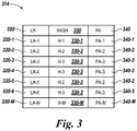
- Figure 3 illustrates a hash table 314 representing a number of logical addresses, hash values, and physical addresses in accordance with one or more embodiments of the present disclosure.
- the hash table 314 in Figure 3 includes a number of columns.
- the first column 320 indicates logical addresses (LAs) of particular portions of data, such as a sector, for example.
- the second column 330 indicates hash values of particular portions of data.
- the third column 340 indicates physical addresses (PAs) of particular portions of data.
- the physical addresses of particular portions of data include a pointer to the physical location of that portion of data in a memory device.
- column 320 includes a number of different logical addresses 320-1 ("LA-1"), 320-2 (“LA-2”), 320-3 (“LA-3"), 320-4 ("LA-4"), 320-5 (“LA-5"), 320-6 (“LA-6”), and 320-M (“LA-M”).
- Each logical address is associated with a respective hash value 330-1 ("H-1"), 330-2 ("H-2”), 330-3 (“H-3"), and 330-M (“H-M”).
- the logical addresses in column 320 of hash table 314 and their associated hash values in column 330 can be associated with physical addresses in column 340 that indicates a physical location of data in a memory system, e.g., system 104 in Figure 1 , associated with the logical addresses in column 320 and the hash values in column 330.
- Each logical address 320-1, 320-2, 320-3, 320-4, 320-5, 320-6, and 320-M and associated hash value 330-1, 330-2, 330-3, and 330-M can have an associated physical address 340-1 ("PA-1"), 340-2 ("PA-2"), 340-3 ("PA-3"), and 340-M ("PA-M").
- the logical addresses sharing a common hash value can be associated with the same physical location. This allows for data associated with two or more logical addresses to be written to the memory devices only once.
- logical address 320-1 is associated with hash value 330-1 and the data associated with logical address 320-1 is at a physical location in a memory device associated with physical address 340-1.
- Logical address 320-2 and logical address 320-5 are associated with hash value 330-2 and the data associated with logical address 320-2 and logical address 320-5 is at a physical location in a memory device associated with physical address 340-2.
- Logical address 320-3, logical address 320-4, and logical address 320-6 are associated with hash value 330-3 and the data associated with logical address 320-3, logical address 320-4, and logical address 320-6 is at a physical location in a memory device associated with physical address 340-3.
- Logical address 320-M is associated with hash value 330-M and the data associated with logical address 320-M is at a physical location in a memory device associated with physical address 340-M.
- the logical address 320-1 is associated with a hash value 330-1 and the data associated with logical address 320-1 is at a physical location in a memory device associated with physical address 340-1.
- any data that is associated with, e.g., part of, a write command received by a memory system that shares a common hash value, e.g., hash value 330-1 will not be written to a memory device, but can have its logical address associated with a common hash value 330-1 and a common physical address 340-1.
- logical addresses 320-2 and 320-5 correspond to identical data, therefore they share a common hash value, hash value 330-2.
- the data associated with logical addresses 320-2 and 320-5 is written once to a physical location associated with physical address 340-2, thus the data associated with the logical addresses 320-2 and 320-5 is only written to the memory devices once.
- any data that is associated with a write command received by a memory system that shares a common hash value, e.g., hash value 330-2 will be associated with a common physical location having a common physical address, e.g., 340-2.
- the hash table 314 can be used to identify the physical location of the data via the physical address 340-2 associated with logical addresses 320-2 and 320-5 and commands to read associated with logical addresses 320-2 and 320-5 can be read from the same physical location.
- the logical addresses 320-3, 320-4, and 320-6 correspond to identical data, therefore they share a common hash value, hash value 330-3.
- the data associated with logical addresses 320-3, 320-4, and 320-6 is written once to a physical location associated with physical address 340-3, thus the data associated with the logical addresses 320-3, 320-4, and 320-6 is only written to the memory devices once.
- any data that is associated with a write command received by a memory system that shares a common hash value, e.g., hash value 330-3 will be associated with a common physical location having a common physical address, e.g., 340-3.
- the hash table 314 can be used to identify the physical location of the data via the physical address 340-3 associated with logical addresses 320-3, 320-4, and 320-6 and commands to read associated with logical addresses 320-3, 320-4, and 320-6 are read from the same physical location.
- a hash table can include hash values and physical locations for data associated with the hash values. In some embodiments, data that is associated with a hash value that exists in a hash table will not be written to a memory device.
- a hash table can include a list of hash values and a list of physical locations associated with each hash value that can be used to determine if data associated with a hash value is located at a physical location in a memory device and if it is not necessary to write the data associated with the hash value in a memory device because it is already located at a physical location in a memory device.
- the present disclosure includes devices and methods for data deduplication.
- One such method includes receiving a write command, transforming data associated with the write command, determining if a transformation value of the data exists in a transformation table, and responsive to a determination that the transformation value does not exist in the transformation table, writing the data associated with the write command to a memory device.
Landscapes
- Engineering & Computer Science (AREA)
- Theoretical Computer Science (AREA)
- Physics & Mathematics (AREA)
- General Engineering & Computer Science (AREA)
- General Physics & Mathematics (AREA)
- Human Computer Interaction (AREA)
- Quality & Reliability (AREA)
- Information Retrieval, Db Structures And Fs Structures Therefor (AREA)
- Memory System (AREA)
Abstract
Description
- The present disclosure relates generally to semiconductor memory devices and methods, and more particularly, to devices and methods for data deduplication.
- Memory devices are typically provided as internal, semiconductor, integrated circuits and/or external removable devices in computers or other electronic devices. There are many different types of memory including random-access memory (RAM), read only memory (ROM), dynamic random access memory (DRAM), synchronous dynamic random access memory (SDRAM), phase change random access memory (PCRAM), and flash memory, among others.
- Memory devices are utilized as non-volatile memory for a wide range of electronic applications in need of high memory densities, high reliability, and low power consumption. Non-volatile memory may be used in a personal computer, a portable memory stick, a solid state drive (SSD), a personal digital assistant (PDA), a digital camera, a cellular telephone, a portable music player e.g., MP3 player, a movie player, and other electronic devices, among others. Data, such as program code, and system data, such as a basic input/output system (BIOS), are typically stored in non-volatile memory devices.
- Memory systems can receive write commands from a host, with the write commands being associated with, e.g., including, data to be written to one or more memory devices of the memory system. The data associated with, e.g., in, a write command can include a number of portions, e.g., sectors, with each portion having a unique logical address associated therewith. Each logical address can be assigned a physical address associated with a physical location, and each portion of data in a write command can be written to a particular physical location associated with the physical address assigned to the logical address corresponding to each portion of the data. In various instances, different logical addresses can correspond to the same physical data such that the data is physically duplicated in one or more memory devices of the memory system. Writing duplicate data can unnecessarily decrease the storage capacity of a memory system, among other drawbacks.
-
-
Figure 1 is a functional block diagram of a computing device including at least one memory system, in accordance with one or more embodiments of the present disclosure. -
Figure 2 is a functional block diagram of a computing device including at least one memory system, in accordance with one or more embodiments of the present disclosure. -
Figure 3 illustrates a hash table representing a number of logical addresses, hash values, and physical addresses in accordance with one or more embodiments of the present disclosure. - The present disclosure includes devices and methods for data deduplication. One such method includes receiving a write command, transforming data associated with, e.g., from, the write command, determining if a transformation value of the data exists in a transformation table, and responsive to a determination that the transformation value does not exist in the transformation table, writing the data associated with the write command to a memory device.
- Data deduplication can include avoiding writing duplicate data to a memory system. In previous approaches, a host would compare files to be written to a memory system with the files on the memory system to determine if a file is already present on the memory system and delete existing duplicate files present on the memory system. In such approaches, if a file was present on the memory system, the host would not send the command to write that file to the memory system, thus avoiding duplication of the file on the memory system. In one or more embodiments, data deduplication can include transforming, e.g., hashing, each sector of data that is received by a memory system from a host. The hashing of each sector of data can include generating a transformation value, e.g., hash value, for each sector of data received in a write command. Embodiments are not limited to hashing each sector of data and data can be hashed in any increment, such as pages, for example.
- In one or more embodiments, the hash values generated for each sector of data can be compared to hash values in a transformation table, e.g., hash table, for data that is currently written to memory devices in a memory system. If a hash value generated for a sector of data received in a write command does not exist, e.g., is not present, in the hash table, the sector of data is written to a location in the memory devices and the hash table is updated by writing an entry to the hash table that includes the hash value of the sector data. The hash table can also be updated by writing an entry to the hash table that includes a logical address of the sector of data and a physical address of the sector of data. If a hash value generated for a sector of data received in a write command does exist in the hash table, the hash table is updated by writing an entry to the hash table to associate the logical address of the sector of data with the hash value of the sector data. A successful write indication can be sent to the host when the hash table is updated with the hash value and a logical address and physical address of the sector of data.
- In the following detailed description of the present disclosure, reference is made to the accompanying drawings that form a part hereof, and in which is shown by way of illustration how a number of embodiments of the disclosure may be practiced. These embodiments are described in sufficient detail to enable those of ordinary skill in the art to practice the embodiments of this disclosure, and it is to be understood that other embodiments may be utilized and that process, electrical, and/or structural changes may be made without departing from the scope of the present disclosure.
- As used herein, "a number of' something can refer to one or more such things. For example, a number of memory devices can refer to one or more memory devices. Additionally, the designators "N" and "M" as used herein, particularly with respect to reference numerals in the drawings, indicates that a number of the particular feature so designated can be included with a number of embodiments of the present disclosure.
- The figures herein follow a numbering convention in which the first digit or digits correspond to the drawing figure number and the remaining digits identify an element or component in the drawing. Similar elements or components between different figures may be identified by the use of similar digits. For example, 100 may reference element "00" in
Figure 1 , and a similar element may be referenced as 200 inFigure 2 . As will be appreciated, elements shown in the various embodiments herein can be added, exchanged, and/or eliminated so as to provide a number of additional embodiments of the present disclosure. In addition, as will be appreciated, the proportion and the relative scale of the elements provided in the figures are intended to illustrate the embodiments of the present disclosure, and should not be taken in a limiting sense. -
Figure 1 is a functional block diagram of acomputing device 100 including at least onememory system 104, in accordance with one or more embodiments of the present disclosure. In the embodiment illustrated inFigure 1 , thememory system 104 can include acontroller 108 and one or more memory devices 110-1, ..., 110-N. In this example, thecontroller 108 is external to the one or more memory devices 110-1, ..., 110-N. The memory devices 110-1, .. ., 110-N can provide a storage volume for the memory system, e.g., with a file system formatted to the memory devices. Thecontroller 108 can include control circuitry, e.g., hardware, firmware, and/or software. In one or more embodiments, thecontroller 108 can be an application specific integrated circuit (ASIC) coupled to a printed circuit board including a physical interface and memory devices 110-1, ..., 110-N. - The
controller 108 can include adata deduplication component 112 and a hash table 114. Thedata deduplication component 112 can include hardware, firmware, and/or software and can perform data deduplication operations on data, e.g., to determine if data exists in the memory devices 110-1, ..., 110-N and if data should be written to the memory devices 110-1, ..., 110-N. The hash table 114 can be stored in memory cells on thecontroller 108 and/or in memory cells of the memory devices 110-1, ..., 110-N and can be used to associate a logical address with a hash value and also with a physical address for a portion of data, such as a sector. The hash table 114 can include a number of entries corresponding to logical addresses, hash values, and physical addresses for portions of data, e.g., sectors. Thedata deduplication component 112 can hash each sector of data that is received by a memory system from a host. While hashing each sector of data, a hash value for each sector of data received in a write command can be generated. - In one or more embodiments,
data deduplication component 112 can compare the hash values generated for each sector of data to hash values in hash table 112 corresponding to data that is currently written to memory devices 110-1,..., 110-N. If a hash value generated for a sector of data received in a write command does not exist in hash table 114, the sector of data is written to a location in memory devices 110-1, ..., 110-N and hash table 114 is updated by writing an entry to hash table 114 with the hash value of the sector of data. Hash table 114 can also be updated by writing an entry to hash table 114 to associate a logical address of the sector of data and a physical address of the sector of data with the hash value of the sector of data. If a hash value generated for a sector of data received in a write command does exist in hash table 114, hash table 114 can be updated by writing an entry to the hash table 114 to associate the logical address of the sector of data with the hash value of the sector data that is already hash table 114. A successful write indication can be sent to thehost 102 when hash table 114 is updated with the hash value and a logical address and physical address of the sector of data. - As illustrated in
Figure 1 , ahost 102 can be coupled to thememory system 104.Host 102 can be a laptop computer, personal computer, digital camera, digital recording and playback device, mobile telephone, PDA, memory card reader, interface hub, among other host systems, and can include a memory access device, e.g., a processor. One of ordinary skill in the art will appreciate that "a processor" can intend one or more processors, such as a parallel processing system, a number of coprocessors, etc. - In one or more embodiments, a physical host interface can be in the form of a standardized interface. For example, when the
memory system 104 is used for data storage in acomputing device 100, a physical host interface can be a serial advanced technology attachment (SATA), peripheral component interconnect express (PCIe), or a universal serial bus (USB), among other interfaces. In general, however, a physical host interface can provide an interface for passing control, address, data, and other signals between thememory system 104 and ahost 102 having compatible receptors for the physical host interface. Thehost 102 can send write commands to thememory system 104 via physical host interface. - The
controller 108 can communicate with the memory devices 110-1, ..., 110-N to read, write, and erase data, among other operations.Controller 108 can have circuitry that may be one or more integrated circuits and/or discrete components. A memory controller could selectively couple an I/O connection (not shown inFigure 1 ) of a memory device 110-1, ..., 110-N to receive the appropriate signal at the appropriate I/O connection at the appropriate time. Similarly, the communication protocol between ahost 102 and thememory system 104 may be different than what is required for access of a memory device 110-1, ..., 110-N. Controller 108 could then translate the commands received from a host into the appropriate commands to achieve the desired access to a memory device 110-1, ..., 110-N. - A memory device 110-1, ..., 110-N can include one or more arrays of memory cells, e.g., non-volatile memory cells. The arrays can be phase change memory (PCM) arrays, for example. Embodiments are not limited to a particular type of memory device. For instance, the memory device can include RAM, ROM, HDD, DRAM, SDRAM, PCRAM, RRAM, and flash memory, among others.
- The memory devices 110-1, ..., 110-N can include a number of memory cells that can be grouped. As used herein, a group can include one or more memory cells, such as a page, block, plane, die, an entire array, or other groups of memory cells. For example, some memory arrays can include a number of pages of memory cells that make up a block of memory cells. A number of blocks can be included in a plane of memory cells. A number of planes of memory cells can be included on a die. As an example, a 128 GB memory device can include 4314 bytes of data per page, 128 pages per block, 2048 blocks per plane, and 16 planes per device.
- The embodiment of
Figure 1 can include additional circuitry that is not illustrated so as not to obscure embodiments of the present disclosure. For example, thememory system 104 can include a controller, e.g., control circuitry, and address circuitry to latch address signals provided over I/O connections through I/O circuitry. Address signals can be received and decoded by a row decoder and a column decoder to access the memory devices 110-1, ..., 110-N. It will be appreciated by those skilled in the art that the number of address input connections can depend on the density and architecture of the memory devices 110-1, ..., 110-N. - In general, the
controller 108 can be responsible for converting commands received from thehost 102, e.g., from a PCIe bus, into command instructions for host-memory translation circuitry and for converting memory responses into host system commands for transmission to the requesting host. - In one or more embodiments, data can be written to the memory devices one page at a time. Each page in the memory device can have a number of physical sectors and each physical sector can be associated with an LBA. As an example, a physical page can have 8 physical sectors of data. However, embodiments are not limited to a particular number of physical sectors per physical page.
-
Figure 2 is a functional block diagram of acomputing device 200 including at least onememory system 204, in accordance with one or more embodiments of the present disclosure. In the embodiment illustrated inFigure 2 , thememory system 204 can include acontroller 208 and one or more memory devices 210-1, ..., 210-N. In this example, thecontroller 208 is external to the one or more memory devices 210-1, ..., 210-N, but in other embodiments the controller could be internal to one or more of the memory device or distributed between one or more of the memory devices and/or thecontroller 208. The memory devices 210-1, ..., 210-N can provide a storage volume for the memory system, e.g., with a file system formatted to the memory devices. Thecontroller 208 can include control circuitry, e.g., hardware, firmware, and/or software. In one or more embodiments, thecontroller 208 can be an application specific integrated circuit (ASIC) coupled to a printed circuit board including a physical interface and memory devices 210-1, ..., 210-N. - The memory devices 210-1, ..., 210-N can include a
data deduplication component 212, such as part of an internal controller ,e.g., control circuitry. Thedata deduplication component 212 can include hardware, firmware, and/or software and can perform data deduplication operations on data, as discussed above in association withFigure 1 . The memory devices 210-1, ..., 210-N can include a hash table 214. The hash table can stored in memory cells of the memory devices 210-1, ..., 210-N and can be used to associate a logical address with a hash value and also with a physical address for a portion of data, such as a sector, as discussed above in association withFigure 1 . - The
controller 208 can communicate with the memory devices 210-1, ..., 210-N to read, write, and erase data, among other operations.Controller 208 can have circuitry that may be one or more integrated circuits and/or discrete components. A memory controller could selectively couple an I/O connection (not shown inFigure 1 ) of a memory device 210-1, ..., 210-N to receive the appropriate signal at the appropriate I/O connection at the appropriate time. Similarly, the communication protocol between ahost 202 and thememory system 204 may be different than what is required for access of a memory device 210-1, ..., 210-N. Controller 208 could then translate the commands received from a host into the appropriate commands to achieve the desired access to a memory device 210-1, ..., 210-N. - A memory device 210-1, ..., 210-N can include one or more arrays of memory cells, e.g., non-volatile memory cells. The arrays can be phase change memory (PCM) arrays, for example. Embodiments are not limited to a particular type of memory device. For instance, the memory device can include RAM, ROM, DRAM, SDRAM, PCRAM, RRAM, and flash memory, among others.
- The memory devices 210-1, ..., 210-N can include a number of memory cells that can be grouped. As used herein, a group can include one or more memory cells, such as a page, block, plane, die, an entire array, or other groups of memory cells. For example, some memory arrays can include a number of pages of memory cells that make up a block of memory cells. A number of blocks can be included in a plane of memory cells. A number of planes of memory cells can be included on a die. As an example, a 128 GB memory device can include 4314 bytes of data per page, 128 pages per block, 2048 blocks per plane, and 16 planes per device.
-
Figure 3 illustrates a hash table 314 representing a number of logical addresses, hash values, and physical addresses in accordance with one or more embodiments of the present disclosure. The hash table 314 inFigure 3 includes a number of columns. Thefirst column 320 indicates logical addresses (LAs) of particular portions of data, such as a sector, for example. Thesecond column 330 indicates hash values of particular portions of data. Thethird column 340 indicates physical addresses (PAs) of particular portions of data. The physical addresses of particular portions of data include a pointer to the physical location of that portion of data in a memory device. - In the example shown in
Figure 3 ,column 320 includes a number of different logical addresses 320-1 ("LA-1"), 320-2 ("LA-2"), 320-3 ("LA-3"), 320-4 ("LA-4"), 320-5 ("LA-5"), 320-6 ("LA-6"), and 320-M ("LA-M"). Each logical address is associated with a respective hash value 330-1 ("H-1"), 330-2 ("H-2"), 330-3 ("H-3"), and 330-M ("H-M"). - In one or more embodiments, the logical addresses in
column 320 of hash table 314 and their associated hash values incolumn 330 can be associated with physical addresses incolumn 340 that indicates a physical location of data in a memory system, e.g.,system 104 inFigure 1 , associated with the logical addresses incolumn 320 and the hash values incolumn 330. Each logical address 320-1, 320-2, 320-3, 320-4, 320-5, 320-6, and 320-M and associated hash value 330-1, 330-2, 330-3, and 330-M can have an associated physical address 340-1 ("PA-1"), 340-2 ("PA-2"), 340-3 ("PA-3"), and 340-M ("PA-M"). The logical addresses sharing a common hash value can be associated with the same physical location. This allows for data associated with two or more logical addresses to be written to the memory devices only once. - In the example shown in
Figure 3 , logical address 320-1 is associated with hash value 330-1 and the data associated with logical address 320-1 is at a physical location in a memory device associated with physical address 340-1. Logical address 320-2 and logical address 320-5 are associated with hash value 330-2 and the data associated with logical address 320-2 and logical address 320-5 is at a physical location in a memory device associated with physical address 340-2. - Logical address 320-3, logical address 320-4, and logical address 320-6 are associated with hash value 330-3 and the data associated with logical address 320-3, logical address 320-4, and logical address 320-6 is at a physical location in a memory device associated with physical address 340-3. Logical address 320-M is associated with hash value 330-M and the data associated with logical address 320-M is at a physical location in a memory device associated with physical address 340-M.
- The logical address 320-1 is associated with a hash value 330-1 and the data associated with logical address 320-1 is at a physical location in a memory device associated with physical address 340-1. In some embodiments, any data that is associated with, e.g., part of, a write command received by a memory system that shares a common hash value, e.g., hash value 330-1, will not be written to a memory device, but can have its logical address associated with a common hash value 330-1 and a common physical address 340-1.
- In this example, logical addresses 320-2 and 320-5 correspond to identical data, therefore they share a common hash value, hash value 330-2. The data associated with logical addresses 320-2 and 320-5 is written once to a physical location associated with physical address 340-2, thus the data associated with the logical addresses 320-2 and 320-5 is only written to the memory devices once. In some embodiments, any data that is associated with a write command received by a memory system that shares a common hash value, e.g., hash value 330-2, will be associated with a common physical location having a common physical address, e.g., 340-2. When the data associated with logical addresses 320-2 and 320-5, are accessed, e.g., requested in read commands, the hash table 314 can be used to identify the physical location of the data via the physical address 340-2 associated with logical addresses 320-2 and 320-5 and commands to read associated with logical addresses 320-2 and 320-5 can be read from the same physical location.
- In this example, the logical addresses 320-3, 320-4, and 320-6 correspond to identical data, therefore they share a common hash value, hash value 330-3. The data associated with logical addresses 320-3, 320-4, and 320-6 is written once to a physical location associated with physical address 340-3, thus the data associated with the logical addresses 320-3, 320-4, and 320-6 is only written to the memory devices once. In some embodiments, any data that is associated with a write command received by a memory system that shares a common hash value, e.g., hash value 330-3, will be associated with a common physical location having a common physical address, e.g., 340-3. When the data associated with logical addresses 320-3, 320-4, and 320-6, are accessed, e.g., requested in read commands, the hash table 314 can be used to identify the physical location of the data via the physical address 340-3 associated with logical addresses 320-3, 320-4, and 320-6 and commands to read associated with logical addresses 320-3, 320-4, and 320-6 are read from the same physical location.
- In one or more embodiments, a hash table can include hash values and physical locations for data associated with the hash values. In some embodiments, data that is associated with a hash value that exists in a hash table will not be written to a memory device. A hash table can include a list of hash values and a list of physical locations associated with each hash value that can be used to determine if data associated with a hash value is located at a physical location in a memory device and if it is not necessary to write the data associated with the hash value in a memory device because it is already located at a physical location in a memory device.
- The present disclosure includes devices and methods for data deduplication. One such method includes receiving a write command, transforming data associated with the write command, determining if a transformation value of the data exists in a transformation table, and responsive to a determination that the transformation value does not exist in the transformation table, writing the data associated with the write command to a memory device.
- Although specific embodiments have been illustrated and described herein, those of ordinary skill in the art will appreciate that an arrangement calculated to achieve the same results can be substituted for the specific embodiments shown. This disclosure is intended to cover adaptations or variations of a number of embodiments of the present disclosure. It is to be understood that the above description has been made in an illustrative fashion, and not a restrictive one. Combination of the above embodiments, and other embodiments not specifically described herein will be apparent to those of ordinary skill in the art upon reviewing the above description. The scope of a number of embodiments of the present disclosure includes other applications in which the above structures and methods are used. Therefore, the scope of a number of embodiments of the present disclosure should be determined with reference to the appended claims, along with the full range of equivalents to which such claims are entitled.
- In the foregoing Detailed Description, some features are grouped together in a single embodiment for the purpose of streamlining the disclosure. This method of disclosure is not to be interpreted as reflecting an intention that the disclosed embodiments of the present disclosure have to use more features than are expressly recited in each claim. Rather, as the following claims reflect, inventive subject matter lies in less than all features of a single disclosed embodiment. Thus, the following claims are hereby incorporated into the Detailed Description, with each claim standing on its own as a separate embodiment.
- The following clauses set out additional embodiments of the invention.
-
Clause 1. A method for data deduplication,
comprising: receiving a write command;- transforming data associated with the write command;
- determining if a transformation value of the data exists in a transformation table; and
- responsive to a determination that the transformation value does not exist in the transformation table, writing the data associated with the write command to a memory device.
-
Clause 2. The method ofclause 1, wherein receiving the write command includes receiving the write command from a host. -
Clause 3. The method ofclause 1, wherein determining if a transformation value of the data exists in a transformation table includes determining if a transformation value of the data associated with the write command exists in a transformation table stored in the memory device. -
Clause 4. The method ofclause 1, wherein determining if a transformation value of the data exists in a transformation table includes determining if a transformation value of the data associated with the write command exists in a transformation table stored in a controller of the memory device. -
Clause 5. The method of any one of clauses 1-4, wherein the data includes a number of portions of data and the method further includes writing the transformation value of a portion of the data to the transformation table. -
Clause 6. The method of any one of clauses 1-4, wherein the data includes a number of portions of data and the method further includes associating the transformation value and a physical address of a portion of the data together via the transformation table. - Clause 7. The method of any one of clauses 1-4, wherein the data includes a number of portions of data and transforming data associated with the write command includes hashing each portion of the data associated with the write command.
- Clause 8. A method for data deduplication,
comprising: hashing data associated with a write
command;- determining if a hash value of the data associated with the write command exists in a hash table; and
- writing data associated with the write command to a memory device if the hash value of the data is not in the hash table.
- Clause 9. The method of clause 8, wherein the data includes anumber of portions of data and hashing data associated with the write command includes hashing each portion of data associated with the write command.
- Clause 10. The method of clause 9, including writing, to the hash table, the hash value of each portion of the data associated with the write command that is not in the hash table.
- Clause 11. The method of clause 10, wherein writing, to the hash table, the hash value of each portion of the data associated with the write command that is not in the hash table includes writing to phase change memory cells.
- Clause 12. The method of any one of clauses 8-11, further including sending a successful write indication to a host if the hash value of the data exists in the hash table and associating a logical address of the data with the hash value that exists in the hash table.
- Clause 13. The method of any one of clauses 8-11, wherein determining if ahash value of the data associated with the write command exists in a hash table includes determining if the hash value of the data associated with the write command exists in the hash table via data deduplication circuitry of the controller of the memory device.
- Clause 14. A method for data deduplication, comprising:
- hashing data associated with a write command, wherein the data includes a number of portions of data;
- determining if a hash value of each portion of data associated with the write command exists in a hash table;
- responsive to a determination that a hash value exists in the hash table, sending a successful write indication to a host if the hash value of the data exists in the hash table; and
- responsive to a determination that a hash value does not exist in the hash table, writing data associated with the write command to the memory device.
- Clause 15. The method of clause 14, the method further includes associating a logical address of each portion of the data with the hash value of each portion of the data that exists in the hash table.
- Clause 16. The method of clause 14, the method further includes associating a logical address of each portion of the data with the hash value of each portion of the data and with a physical address of each portion of the data via the hash table.
- Clause 17. The method of any oneof clauses 14-16, further including writing, to the hash table, the hash value of each portion not in the hash table.
- Clause 18. The method of any one of clauses 14-16, further including associating a number of logical addresses that share a common hash value with a common physical location in the memory device via the hash table.
- Clause 19. A device, comprising:
- an array of memory cells; and
- a controller coupled to the array and configured to: receive a write command; hash data associated with the write command;
- determine if a hash value of the data associated with the write command exists in a hash table; and
write the data associated with the write command corresponding to the hash value that does not exist in the hash table to the array of memory cells only if it is determined that the hash value does not exist in the hash table.
- Clause 20. The device of clause 19, wherein the controller is external to a memory device including the array.
- Clause 21. The device of clause 19, wherein the controller is internal to a memory device including the array.
- Clause 22. The device of clause 19, wherein the hash table is stored in the controller.
- Clause 23. The device of clause 19, wherein the hash table is stored in the array.
- Clause 24. The device of clause 19, wherein the data includes a number of portions of data and the controller is configured to send a successful write indication to a host responsive to a determination that the hash value exists in the hash table and associate a logical address of a portion of data with the hash value that exists in the hash table.
- Clause 25. The device of any one of clauses 19-24, wherein the array of memory cells includes phase change memory cells.
- Clause 26. The device of any one of clauses 19-24, wherein the array of memory cells includes flash memory cells.
- Clause 27. The device of any one of clauses 19-24, wherein the data includes a number of portions of data and the hash table associates a logical address of a portion of data with a physical address of the portion of data via a hash value.
- Clause 28. A device, comprising:
- an array of memory cells; and
- a controller coupled to the array and configured to:
hash data associated with a write command received from a host, wherein the data includes a number of portions of data;- determine if a hash value of each portion of data associated with the write command exists in a hash table;
- send a successful write indication to the host for a portion of data if a hash value for the portion of data exists in the hash table; and
- write the portion of data to the device if the hash value of the portion of data is not in the hash table.
- Clause 29. The device of clause 28, wherein the controller configured to determine if the hash value of each portion of data associated with the write command exists in the hash table comprises data deduplication circuitry.
- Clause 30. The device of clause 28, wherein the hash table is stored in flash memory cells.
- Clause 31. The device of any one of clauses 28-30, wherein the controller is configured to write the hash value of each portion of data to the hash table if it is determined the hash value does not exist in the hash table.
- Clause 32. A device, comprising:
- an array of memory cells; and
- a controller coupled to the array configured to:
- hash data associated with a number of portions of data associated with a write command;
- for each portion of the number of portions, determine whether a hash value associated with the portion exists in a hash table; and
- for only those portions of data whose hash value is determined to not exist in the hash table, write data corresponding to those portions of data in the array.
- Clause 33. The device of clause 32, wherein the array of memory cells is a phase change memory array.
Claims (15)
- A method for data deduplication, comprising:translating a write command into a number of memory device write commands that each include instructions that, when executed, cause a memory device to perform a write operation which writes a particular amount of data to the memory device;transforming data associated with the write command by creating a number of transformation values for the data, wherein each of the number of transformation values correspond to a portion of data that is less data than the particular amount of data;identifying a portion of the number of transformation values that do not exist in a transformation table;determining that data associated with the portion of the number of transformation values does not exist in the memory device responsive to identifying those of the number of transformation values do not exist in a transformation table; andexecuting at least a portion of the write command by writing the particular amount of data to the memory device.
- The method of claim 1, wherein writing the particular amount of data includes only writing data associated with the command having transformation values that do not exist in the transformation table.
- The method of claim 1, further including skipping writing data associated with the command with transformation values that exist in the transformation table.
- The method of claim 1, wherein identifying the portion of the number of transformation values that that do not exist in the transformation table includes locating transformation values in the transformation table stored in the memory device.
- The method of claim 1, wherein the method further includes writing the number of transformation values to the transformation table.
- The method of claim 1, wherein the method further includes associating each of the number of transformation values and a particular physical address via the transformation table.
- The method of claim 1, wherein transforming data associated with the write command includes hashing the data associated with the write command.
- The method of claim 1, wherein executing at least the portion of the write command includes performing memory device write commands to write the data associated with the portion of the number of transformation values does not exist in the memory device in increments of the particular amount data.
- An apparatus, comprising:an array of memory cells; anda controller coupled to the array and configured to:hash data associated with a write command received from a host;wherein the controller translates the write command into a number of memory device write commands that each include instructions that, when executed by the controller, cause the array of memory cells to perform a write operation which writes a particular amount of data to the array of memory cells;wherein the data includes a number of portions of data that are each an amount of data that is less than the particular amount of data written via the write operation;wherein a hash value for each of the number of portions of data is created, andexecute the write operation by writing the particular amount of data to the array of memory cells.
- The apparatus of claim 9, wherein the controller configured to execute the write operation by writing the particular amount of data to the array of memory cells comprises only writing portions of data having hash values that are not in a hash table.
- The apparatus of claim 9, wherein the controller is configured to skip writing portions of data having hash values in the hash table.
- The apparatus of claim 9, wherein the controller is configured to send a successful write indication to a host for portions of data having hash values in the hash table.
- The apparatus of claim 9, wherein the controller is configured to associate logical addresses of portions of data having hash values in the hash table with the hash values that exists in the hash table.
- The apparatus of claim 9, wherein the controller is configured to determine if hash values exist in the hash table via data deduplication circuitry.
- The apparatus of claim 9, wherein the number of portions of data are sectors of data and the particular amount of data written via the write operation is a page of data.
Applications Claiming Priority (3)
| Application Number | Priority Date | Filing Date | Title |
|---|---|---|---|
| US13/083,269 US9223511B2 (en) | 2011-04-08 | 2011-04-08 | Data deduplication |
| PCT/US2012/030713 WO2012138504A2 (en) | 2011-04-08 | 2012-03-27 | Data deduplication |
| EP12767450.5A EP2695065A4 (en) | 2011-04-08 | 2012-03-27 | DEDUPLICATION OF DATA |
Related Parent Applications (1)
| Application Number | Title | Priority Date | Filing Date |
|---|---|---|---|
| EP12767450.5A Division EP2695065A4 (en) | 2011-04-08 | 2012-03-27 | DEDUPLICATION OF DATA |
Publications (1)
| Publication Number | Publication Date |
|---|---|
| EP3859534A1 true EP3859534A1 (en) | 2021-08-04 |
Family
ID=46966999
Family Applications (2)
| Application Number | Title | Priority Date | Filing Date |
|---|---|---|---|
| EP12767450.5A Ceased EP2695065A4 (en) | 2011-04-08 | 2012-03-27 | DEDUPLICATION OF DATA |
| EP21164611.2A Pending EP3859534A1 (en) | 2011-04-08 | 2012-03-27 | Data deduplication |
Family Applications Before (1)
| Application Number | Title | Priority Date | Filing Date |
|---|---|---|---|
| EP12767450.5A Ceased EP2695065A4 (en) | 2011-04-08 | 2012-03-27 | DEDUPLICATION OF DATA |
Country Status (7)
| Country | Link |
|---|---|
| US (3) | US9223511B2 (en) |
| EP (2) | EP2695065A4 (en) |
| JP (2) | JP2014513345A (en) |
| KR (1) | KR101532862B1 (en) |
| CN (1) | CN103518193B (en) |
| TW (1) | TWI536384B (en) |
| WO (1) | WO2012138504A2 (en) |
Families Citing this family (45)
| Publication number | Priority date | Publication date | Assignee | Title |
|---|---|---|---|---|
| US9223511B2 (en) * | 2011-04-08 | 2015-12-29 | Micron Technology, Inc. | Data deduplication |
| US11636031B2 (en) * | 2011-08-11 | 2023-04-25 | Pure Storage, Inc. | Optimized inline deduplication |
| KR20130064518A (en) * | 2011-12-08 | 2013-06-18 | 삼성전자주식회사 | Storage device and operation method thereof |
| US9606910B2 (en) * | 2013-01-17 | 2017-03-28 | Hitachi, Ltd. | Method and apparatus for data reduction |
| US20140281155A1 (en) * | 2013-03-14 | 2014-09-18 | Lsi Corporation | Storage device assisted data de-duplication |
| US9619167B2 (en) * | 2013-11-27 | 2017-04-11 | Intel Corporation | System and method for computing message digests |
| KR102187127B1 (en) * | 2013-12-03 | 2020-12-04 | 삼성전자주식회사 | Deduplication method using data association and system thereof |
| KR102140792B1 (en) | 2013-12-24 | 2020-08-03 | 삼성전자주식회사 | Methods for operating data storage device capable of data de-duplication |
| US8935463B1 (en) * | 2014-01-03 | 2015-01-13 | Fastor Systems, Inc. | Compute engine in a smart SSD exploiting locality of data |
| US9141292B2 (en) | 2014-01-03 | 2015-09-22 | Smart High Reliability Solutions Llc | Enhanced interface to firmware operating in a solid state drive |
| US10176117B2 (en) * | 2014-10-01 | 2019-01-08 | Cacheio Llc | Efficient metadata in a storage system |
| US9626121B2 (en) * | 2014-12-19 | 2017-04-18 | International Business Machines Corporation | De-duplication as part of other routinely performed processes |
| US9934236B2 (en) | 2015-02-23 | 2018-04-03 | International Business Machines Corporation | Streamlining data deduplication |
| US9665287B2 (en) | 2015-09-18 | 2017-05-30 | Alibaba Group Holding Limited | Data deduplication using a solid state drive controller |
| JP6561765B2 (en) * | 2015-10-23 | 2019-08-21 | 富士通株式会社 | Storage control device and storage control program |
| US9690512B2 (en) | 2015-11-23 | 2017-06-27 | Samsung Electronics Co., Ltd. | Method of similarity testing by syndromes and apparatus therefore |
| US9841918B2 (en) * | 2015-12-02 | 2017-12-12 | Samsung Electronics Co., Ltd. | Flash memory device including deduplication, and related methods |
| US10055368B2 (en) * | 2016-02-26 | 2018-08-21 | Sandisk Technologies Llc | Mobile device and method for synchronizing use of the mobile device's communications port among a plurality of applications |
| US10437785B2 (en) | 2016-03-29 | 2019-10-08 | Samsung Electronics Co., Ltd. | Method and apparatus for maximized dedupable memory |
| US10496543B2 (en) * | 2016-03-31 | 2019-12-03 | Samsung Electronics Co., Ltd. | Virtual bucket multiple hash tables for efficient memory in-line deduplication application |
| US10162554B2 (en) * | 2016-08-03 | 2018-12-25 | Samsung Electronics Co., Ltd. | System and method for controlling a programmable deduplication ratio for a memory system |
| TWI610219B (en) * | 2016-08-09 | 2018-01-01 | 捷鼎國際股份有限公司 | Data storage system |
| US10261876B2 (en) * | 2016-11-08 | 2019-04-16 | Micron Technology, Inc. | Memory management |
| KR102509913B1 (en) * | 2017-01-25 | 2023-03-14 | 삼성전자주식회사 | Method and apparatus for maximized dedupable memory |
| KR102849632B1 (en) | 2017-01-25 | 2025-08-26 | 삼성전자주식회사 | Storage device performing hashing-based translation between logical address and physical address |
| US10268413B2 (en) * | 2017-01-27 | 2019-04-23 | Samsung Electronics Co., Ltd. | Overflow region memory management |
| US10282125B2 (en) * | 2017-04-17 | 2019-05-07 | International Business Machines Corporation | Distributed content deduplication using hash-trees with adaptive resource utilization in distributed file systems |
| KR102419136B1 (en) | 2017-06-15 | 2022-07-08 | 삼성전자주식회사 | Image processing apparatus and method using multiple-channel feature map |
| US10521617B2 (en) * | 2017-08-14 | 2019-12-31 | Western Digital Technologies, Inc. | Non-volatile memory device with secure read |
| US11068606B2 (en) * | 2017-09-20 | 2021-07-20 | Citrix Systems, Inc. | Secured encrypted shared cloud storage |
| JP2019057172A (en) | 2017-09-21 | 2019-04-11 | 東芝メモリ株式会社 | Memory system and control method |
| US10706005B2 (en) * | 2017-12-08 | 2020-07-07 | Vmware, Inc. | File system interface for remote direct memory access |
| US10366011B1 (en) * | 2018-05-03 | 2019-07-30 | EMC IP Holding Company LLC | Content-based deduplicated storage having multilevel data cache |
| US10705753B2 (en) | 2018-05-04 | 2020-07-07 | EMC IP Holding Company LLC | Fan-out asynchronous replication logical level caching |
| US10860239B2 (en) | 2018-05-04 | 2020-12-08 | EMC IP Holding Company LLC | Fan-out asynchronous replication caching |
| US10592166B2 (en) | 2018-08-01 | 2020-03-17 | EMC IP Holding Company LLC | Fast input/output in a content-addressable storage architecture with paged metadata |
| US10789062B1 (en) * | 2019-04-18 | 2020-09-29 | Dell Products, L.P. | System and method for dynamic data deduplication for firmware updates |
| US11436165B2 (en) * | 2019-05-01 | 2022-09-06 | Samsung Electronics Co., Ltd. | High bandwidth memory system |
| KR102810527B1 (en) | 2019-09-23 | 2025-05-22 | 삼성전자주식회사 | Storage device and operating method thereof |
| CN111737164B (en) * | 2019-12-31 | 2024-07-23 | 极海微电子股份有限公司 | Access request response method, consumable chip and storage medium |
| CN113568561B (en) * | 2020-04-29 | 2024-05-17 | 伊姆西Ip控股有限责任公司 | Method for information processing, electronic device, and computer storage medium |
| CN111968696B (en) * | 2020-08-27 | 2021-07-06 | 海光信息技术股份有限公司 | Read-only memory circuit and design method thereof, read-only memory and electronic equipment |
| TWI760880B (en) * | 2020-10-07 | 2022-04-11 | 瑞昱半導體股份有限公司 | Storage-device-associated transmission control circuit, data transmission system and method for operating a data transmission system |
| CN114372009B (en) * | 2020-10-15 | 2024-10-11 | 瑞昱半导体股份有限公司 | Transmission control circuit, data transmission system and method for operating data transmission system |
| KR102467372B1 (en) | 2022-01-06 | 2022-11-14 | 삼성전자주식회사 | Storage device and method of operating the same |
Citations (3)
| Publication number | Priority date | Publication date | Assignee | Title |
|---|---|---|---|---|
| US20080294696A1 (en) * | 2007-05-22 | 2008-11-27 | Yuval Frandzel | System and method for on-the-fly elimination of redundant data |
| WO2009117251A1 (en) * | 2008-03-19 | 2009-09-24 | Rambus Inc. | Optimizing storage of common patterns in flash memory |
| US20100250896A1 (en) * | 2009-03-30 | 2010-09-30 | Hi/Fn, Inc. | System and method for data deduplication |
Family Cites Families (19)
| Publication number | Priority date | Publication date | Assignee | Title |
|---|---|---|---|---|
| JPH08185271A (en) | 1994-12-27 | 1996-07-16 | Internatl Business Mach Corp <Ibm> | Data processing method for disk device and disk device |
| US7010645B2 (en) | 2002-12-27 | 2006-03-07 | International Business Machines Corporation | System and method for sequentially staging received data to a write cache in advance of storing the received data |
| US20050152192A1 (en) | 2003-12-22 | 2005-07-14 | Manfred Boldy | Reducing occupancy of digital storage devices |
| US7266657B2 (en) | 2004-10-27 | 2007-09-04 | Kwok-Yan Leung | Data protection device and method of securing data |
| US8165221B2 (en) | 2006-04-28 | 2012-04-24 | Netapp, Inc. | System and method for sampling based elimination of duplicate data |
| US7747584B1 (en) | 2006-08-22 | 2010-06-29 | Netapp, Inc. | System and method for enabling de-duplication in a storage system architecture |
| WO2008113212A1 (en) | 2007-03-21 | 2008-09-25 | Intel Corporation | Method of managing sectors of a non-volatile memory |
| CN100576207C (en) | 2007-05-29 | 2009-12-30 | 北大方正集团有限公司 | A Method for Deduplicating Objects Based on Metadata |
| EP2012235A2 (en) * | 2007-07-06 | 2009-01-07 | Prostor Systems, Inc. | Commonality factoring |
| JP5026213B2 (en) | 2007-09-28 | 2012-09-12 | 株式会社日立製作所 | Storage apparatus and data deduplication method |
| JP5275692B2 (en) * | 2007-10-24 | 2013-08-28 | 株式会社日立製作所 | Storage system group |
| US9164941B2 (en) | 2007-10-24 | 2015-10-20 | Hitachi, Ltd. | Storage system group |
| US7870105B2 (en) * | 2007-11-20 | 2011-01-11 | Hitachi, Ltd. | Methods and apparatus for deduplication in storage system |
| US7908436B1 (en) * | 2008-04-25 | 2011-03-15 | Netapp, Inc. | Deduplication of data on disk devices using low-latency random read memory |
| US8412677B2 (en) * | 2008-11-26 | 2013-04-02 | Commvault Systems, Inc. | Systems and methods for byte-level or quasi byte-level single instancing |
| US20110055471A1 (en) * | 2009-08-28 | 2011-03-03 | Jonathan Thatcher | Apparatus, system, and method for improved data deduplication |
| CN102741800B (en) | 2009-09-18 | 2015-11-25 | 株式会社日立制作所 | Delete the storage system copying data |
| US8352447B2 (en) * | 2011-03-01 | 2013-01-08 | Hitachi, Ltd. | Method and apparatus to align and deduplicate objects |
| US9223511B2 (en) * | 2011-04-08 | 2015-12-29 | Micron Technology, Inc. | Data deduplication |
-
2011
- 2011-04-08 US US13/083,269 patent/US9223511B2/en active Active
-
2012
- 2012-03-27 WO PCT/US2012/030713 patent/WO2012138504A2/en not_active Ceased
- 2012-03-27 JP JP2014503683A patent/JP2014513345A/en active Pending
- 2012-03-27 CN CN201280023074.6A patent/CN103518193B/en active Active
- 2012-03-27 EP EP12767450.5A patent/EP2695065A4/en not_active Ceased
- 2012-03-27 EP EP21164611.2A patent/EP3859534A1/en active Pending
- 2012-03-27 KR KR1020137028250A patent/KR101532862B1/en active Active
- 2012-04-06 TW TW101112336A patent/TWI536384B/en active
-
2015
- 2015-07-10 JP JP2015138522A patent/JP6106719B2/en active Active
- 2015-12-03 US US14/957,801 patent/US9778874B2/en active Active
-
2017
- 2017-08-29 US US15/689,626 patent/US10282128B2/en active Active
Patent Citations (3)
| Publication number | Priority date | Publication date | Assignee | Title |
|---|---|---|---|---|
| US20080294696A1 (en) * | 2007-05-22 | 2008-11-27 | Yuval Frandzel | System and method for on-the-fly elimination of redundant data |
| WO2009117251A1 (en) * | 2008-03-19 | 2009-09-24 | Rambus Inc. | Optimizing storage of common patterns in flash memory |
| US20100250896A1 (en) * | 2009-03-30 | 2010-09-30 | Hi/Fn, Inc. | System and method for data deduplication |
Also Published As
| Publication number | Publication date |
|---|---|
| WO2012138504A3 (en) | 2012-12-27 |
| CN103518193A (en) | 2014-01-15 |
| EP2695065A2 (en) | 2014-02-12 |
| KR20130142182A (en) | 2013-12-27 |
| JP6106719B2 (en) | 2017-04-05 |
| TW201250688A (en) | 2012-12-16 |
| US10282128B2 (en) | 2019-05-07 |
| WO2012138504A2 (en) | 2012-10-11 |
| CN103518193B (en) | 2016-10-12 |
| US20170364301A1 (en) | 2017-12-21 |
| US9778874B2 (en) | 2017-10-03 |
| US20160085474A1 (en) | 2016-03-24 |
| TWI536384B (en) | 2016-06-01 |
| US9223511B2 (en) | 2015-12-29 |
| JP2014513345A (en) | 2014-05-29 |
| KR101532862B1 (en) | 2015-06-30 |
| JP2015212971A (en) | 2015-11-26 |
| EP2695065A4 (en) | 2014-08-20 |
| US20120260021A1 (en) | 2012-10-11 |
Similar Documents
| Publication | Publication Date | Title |
|---|---|---|
| EP3859534A1 (en) | Data deduplication | |
| US10853238B2 (en) | Unaligned data coalescing | |
| TWI507869B (en) | System,apparatus,and method for virtualizing storage devices | |
| US10628326B2 (en) | Logical to physical mapping | |
| EP4357926B1 (en) | Systems, devices, memory controllers, and methods for controlling memory | |
| US9189397B2 (en) | Data storage device including buffer memory | |
| CN107632939A (en) | Mapping table for storage device | |
| US10657052B2 (en) | Information handling system with priority based cache flushing of flash dual in-line memory module pool | |
| US11966631B2 (en) | Command queue order adjustment in a data storage device | |
| US9940052B2 (en) | Memory device configuration commands | |
| KR20240006932A (en) | Memory controller and storage device including the same | |
| CN114936007A (en) | Method and device for storing data | |
| EP4278263B1 (en) | Persistence logging over nvm express for storage devices application | |
| US10846020B2 (en) | Drive assisted storage controller system and method | |
| KR20250131495A (en) | Nonvolatile memory device, method of operating the same, and memory system including the same |
Legal Events
| Date | Code | Title | Description |
|---|---|---|---|
| PUAI | Public reference made under article 153(3) epc to a published international application that has entered the european phase |
Free format text: ORIGINAL CODE: 0009012 |
|
| STAA | Information on the status of an ep patent application or granted ep patent |
Free format text: STATUS: REQUEST FOR EXAMINATION WAS MADE |
|
| 17P | Request for examination filed |
Effective date: 20210324 |
|
| AC | Divisional application: reference to earlier application |
Ref document number: 2695065 Country of ref document: EP Kind code of ref document: P |
|
| AK | Designated contracting states |
Kind code of ref document: A1 Designated state(s): AL AT BE BG CH CY CZ DE DK EE ES FI FR GB GR HR HU IE IS IT LI LT LU LV MC MK MT NL NO PL PT RO RS SE SI SK SM TR |
|
| STAA | Information on the status of an ep patent application or granted ep patent |
Free format text: STATUS: EXAMINATION IS IN PROGRESS |
|
| 17Q | First examination report despatched |
Effective date: 20230712 |