EP3855524A1 - Light emitting diode and display device including the same - Google Patents
Light emitting diode and display device including the same Download PDFInfo
- Publication number
- EP3855524A1 EP3855524A1 EP21152336.0A EP21152336A EP3855524A1 EP 3855524 A1 EP3855524 A1 EP 3855524A1 EP 21152336 A EP21152336 A EP 21152336A EP 3855524 A1 EP3855524 A1 EP 3855524A1
- Authority
- EP
- European Patent Office
- Prior art keywords
- group
- hole transport
- substituted
- unsubstituted
- transport layer
- Prior art date
- Legal status (The legal status is an assumption and is not a legal conclusion. Google has not performed a legal analysis and makes no representation as to the accuracy of the status listed.)
- Pending
Links
- 230000005525 hole transport Effects 0.000 claims abstract description 321
- -1 amine compound Chemical class 0.000 claims description 116
- 150000001875 compounds Chemical group 0.000 claims description 92
- 125000004432 carbon atom Chemical group C* 0.000 claims description 68
- 125000003118 aryl group Chemical group 0.000 claims description 29
- 125000001072 heteroaryl group Chemical group 0.000 claims description 22
- 125000000217 alkyl group Chemical group 0.000 claims description 20
- 125000003277 amino group Chemical group 0.000 claims description 15
- 125000005843 halogen group Chemical group 0.000 claims description 14
- 229910052805 deuterium Inorganic materials 0.000 claims description 13
- 125000004431 deuterium atom Chemical group 0.000 claims description 13
- 125000004435 hydrogen atom Chemical group [H]* 0.000 claims description 12
- 125000001820 oxy group Chemical group [*:1]O[*:2] 0.000 claims description 12
- 125000005073 adamantyl group Chemical group C12(CC3CC(CC(C1)C3)C2)* 0.000 claims description 11
- 125000000113 cyclohexyl group Chemical group [H]C1([H])C([H])([H])C([H])([H])C([H])(*)C([H])([H])C1([H])[H] 0.000 claims description 11
- 125000004093 cyano group Chemical group *C#N 0.000 claims description 9
- 125000004149 thio group Chemical group *S* 0.000 claims description 8
- 125000003808 silyl group Chemical group [H][Si]([H])([H])[*] 0.000 claims description 7
- 125000000732 arylene group Chemical group 0.000 claims description 6
- 125000003983 fluorenyl group Chemical group C1(=CC=CC=2C3=CC=CC=C3CC12)* 0.000 claims description 6
- 125000005549 heteroarylene group Chemical group 0.000 claims description 6
- 125000001997 phenyl group Chemical group [H]C1=C([H])C([H])=C(*)C([H])=C1[H] 0.000 claims description 6
- 125000000449 nitro group Chemical group [O-][N+](*)=O 0.000 claims description 5
- YJTKZCDBKVTVBY-UHFFFAOYSA-N 1,3-Diphenylbenzene Chemical group C1=CC=CC=C1C1=CC=CC(C=2C=CC=CC=2)=C1 YJTKZCDBKVTVBY-UHFFFAOYSA-N 0.000 claims description 4
- 125000006267 biphenyl group Chemical group 0.000 claims description 4
- 125000005724 cycloalkenylene group Chemical group 0.000 claims description 4
- 125000002993 cycloalkylene group Chemical group 0.000 claims description 4
- 125000000592 heterocycloalkyl group Chemical group 0.000 claims description 4
- 125000006588 heterocycloalkylene group Chemical group 0.000 claims description 4
- 125000002887 hydroxy group Chemical group [H]O* 0.000 claims description 4
- 125000001624 naphthyl group Chemical group 0.000 claims description 4
- 125000005509 dibenzothiophenyl group Chemical group 0.000 claims description 3
- 125000000609 carbazolyl group Chemical group C1(=CC=CC=2C3=CC=CC=C3NC12)* 0.000 claims 1
- 238000000605 extraction Methods 0.000 abstract description 15
- 239000010410 layer Substances 0.000 description 378
- 101100451713 Saccharomyces cerevisiae (strain ATCC 204508 / S288c) HTL1 gene Proteins 0.000 description 47
- 230000000052 comparative effect Effects 0.000 description 30
- CYPYTURSJDMMMP-WVCUSYJESA-N (1e,4e)-1,5-diphenylpenta-1,4-dien-3-one;palladium Chemical compound [Pd].[Pd].C=1C=CC=CC=1\C=C\C(=O)\C=C\C1=CC=CC=C1.C=1C=CC=CC=1\C=C\C(=O)\C=C\C1=CC=CC=C1.C=1C=CC=CC=1\C=C\C(=O)\C=C\C1=CC=CC=C1 CYPYTURSJDMMMP-WVCUSYJESA-N 0.000 description 24
- YXFVVABEGXRONW-UHFFFAOYSA-N Toluene Chemical compound CC1=CC=CC=C1 YXFVVABEGXRONW-UHFFFAOYSA-N 0.000 description 24
- 238000006243 chemical reaction Methods 0.000 description 24
- 239000000463 material Substances 0.000 description 21
- RTZKZFJDLAIYFH-UHFFFAOYSA-N Diethyl ether Chemical compound CCOCC RTZKZFJDLAIYFH-UHFFFAOYSA-N 0.000 description 20
- CSNNHWWHGAXBCP-UHFFFAOYSA-L Magnesium sulfate Chemical compound [Mg+2].[O-][S+2]([O-])([O-])[O-] CSNNHWWHGAXBCP-UHFFFAOYSA-L 0.000 description 20
- 230000015572 biosynthetic process Effects 0.000 description 20
- 238000003786 synthesis reaction Methods 0.000 description 20
- 239000012044 organic layer Substances 0.000 description 16
- MFRIHAYPQRLWNB-UHFFFAOYSA-N sodium tert-butoxide Chemical compound [Na+].CC(C)(C)[O-] MFRIHAYPQRLWNB-UHFFFAOYSA-N 0.000 description 16
- 239000000243 solution Substances 0.000 description 15
- 238000010189 synthetic method Methods 0.000 description 13
- 238000005160 1H NMR spectroscopy Methods 0.000 description 12
- 239000002904 solvent Substances 0.000 description 11
- 125000001424 substituent group Chemical group 0.000 description 11
- XLYOFNOQVPJJNP-UHFFFAOYSA-N water Substances O XLYOFNOQVPJJNP-UHFFFAOYSA-N 0.000 description 11
- 238000001816 cooling Methods 0.000 description 10
- 238000002347 injection Methods 0.000 description 10
- 239000007924 injection Substances 0.000 description 10
- 229910052943 magnesium sulfate Inorganic materials 0.000 description 10
- 229910052751 metal Inorganic materials 0.000 description 10
- 239000002184 metal Substances 0.000 description 10
- 238000010898 silica gel chromatography Methods 0.000 description 10
- 239000000758 substrate Substances 0.000 description 10
- YMWUJEATGCHHMB-UHFFFAOYSA-N Dichloromethane Chemical compound ClCCl YMWUJEATGCHHMB-UHFFFAOYSA-N 0.000 description 9
- 150000001412 amines Chemical class 0.000 description 9
- 238000000034 method Methods 0.000 description 9
- VIJSPAIQWVPKQZ-BLECARSGSA-N (2s)-2-[[(2s)-2-[[(2s)-2-[[(2s)-2-[[(2s)-2-[[(2s)-2-acetamido-5-(diaminomethylideneamino)pentanoyl]amino]-4-methylpentanoyl]amino]-4,4-dimethylpentanoyl]amino]-4-methylpentanoyl]amino]propanoyl]amino]-5-(diaminomethylideneamino)pentanoic acid Chemical compound NC(=N)NCCC[C@@H](C(O)=O)NC(=O)[C@H](C)NC(=O)[C@H](CC(C)C)NC(=O)[C@H](CC(C)(C)C)NC(=O)[C@H](CC(C)C)NC(=O)[C@H](CCCNC(N)=N)NC(C)=O VIJSPAIQWVPKQZ-BLECARSGSA-N 0.000 description 7
- GDUANFXPOZTYKS-UHFFFAOYSA-N 6-bromo-8-[(2,6-difluoro-4-methoxybenzoyl)amino]-4-oxochromene-2-carboxylic acid Chemical compound FC1=CC(OC)=CC(F)=C1C(=O)NC1=CC(Br)=CC2=C1OC(C(O)=O)=CC2=O GDUANFXPOZTYKS-UHFFFAOYSA-N 0.000 description 7
- GUTJITRKAMCHSD-UHFFFAOYSA-N 9,9-dimethylfluoren-2-amine Chemical compound C1=C(N)C=C2C(C)(C)C3=CC=CC=C3C2=C1 GUTJITRKAMCHSD-UHFFFAOYSA-N 0.000 description 7
- 239000002356 single layer Substances 0.000 description 7
- PKMUHQIDVVOXHQ-HXUWFJFHSA-N C[C@H](C1=CC(C2=CC=C(CNC3CCCC3)S2)=CC=C1)NC(C1=C(C)C=CC(NC2CNC2)=C1)=O Chemical compound C[C@H](C1=CC(C2=CC=C(CNC3CCCC3)S2)=CC=C1)NC(C1=C(C)C=CC(NC2CNC2)=C1)=O PKMUHQIDVVOXHQ-HXUWFJFHSA-N 0.000 description 6
- OKTJSMMVPCPJKN-UHFFFAOYSA-N Carbon Chemical compound [C] OKTJSMMVPCPJKN-UHFFFAOYSA-N 0.000 description 6
- 229910052799 carbon Inorganic materials 0.000 description 6
- 229940127573 compound 38 Drugs 0.000 description 6
- 229940126179 compound 72 Drugs 0.000 description 6
- 238000011156 evaluation Methods 0.000 description 6
- 238000004895 liquid chromatography mass spectrometry Methods 0.000 description 6
- PQXKHYXIUOZZFA-UHFFFAOYSA-M lithium fluoride Inorganic materials [Li+].[F-] PQXKHYXIUOZZFA-UHFFFAOYSA-M 0.000 description 6
- 239000000203 mixture Substances 0.000 description 6
- PIDFDZJZLOTZTM-KHVQSSSXSA-N ombitasvir Chemical compound COC(=O)N[C@@H](C(C)C)C(=O)N1CCC[C@H]1C(=O)NC1=CC=C([C@H]2N([C@@H](CC2)C=2C=CC(NC(=O)[C@H]3N(CCC3)C(=O)[C@@H](NC(=O)OC)C(C)C)=CC=2)C=2C=CC(=CC=2)C(C)(C)C)C=C1 PIDFDZJZLOTZTM-KHVQSSSXSA-N 0.000 description 6
- WWTBZEKOSBFBEM-SPWPXUSOSA-N (2s)-2-[[2-benzyl-3-[hydroxy-[(1r)-2-phenyl-1-(phenylmethoxycarbonylamino)ethyl]phosphoryl]propanoyl]amino]-3-(1h-indol-3-yl)propanoic acid Chemical compound N([C@@H](CC=1C2=CC=CC=C2NC=1)C(=O)O)C(=O)C(CP(O)(=O)[C@H](CC=1C=CC=CC=1)NC(=O)OCC=1C=CC=CC=1)CC1=CC=CC=C1 WWTBZEKOSBFBEM-SPWPXUSOSA-N 0.000 description 5
- FMKGJQHNYMWDFJ-CVEARBPZSA-N 2-[[4-(2,2-difluoropropoxy)pyrimidin-5-yl]methylamino]-4-[[(1R,4S)-4-hydroxy-3,3-dimethylcyclohexyl]amino]pyrimidine-5-carbonitrile Chemical compound FC(COC1=NC=NC=C1CNC1=NC=C(C(=N1)N[C@H]1CC([C@H](CC1)O)(C)C)C#N)(C)F FMKGJQHNYMWDFJ-CVEARBPZSA-N 0.000 description 5
- XLOMVQKBTHCTTD-UHFFFAOYSA-N Zinc monoxide Chemical compound [Zn]=O XLOMVQKBTHCTTD-UHFFFAOYSA-N 0.000 description 5
- 229940126208 compound 22 Drugs 0.000 description 5
- 229940127113 compound 57 Drugs 0.000 description 5
- 125000000623 heterocyclic group Chemical group 0.000 description 5
- 230000001976 improved effect Effects 0.000 description 5
- QFLWZFQWSBQYPS-AWRAUJHKSA-N (3S)-3-[[(2S)-2-[[(2S)-2-[5-[(3aS,6aR)-2-oxo-1,3,3a,4,6,6a-hexahydrothieno[3,4-d]imidazol-4-yl]pentanoylamino]-3-methylbutanoyl]amino]-3-(4-hydroxyphenyl)propanoyl]amino]-4-[1-bis(4-chlorophenoxy)phosphorylbutylamino]-4-oxobutanoic acid Chemical compound CCCC(NC(=O)[C@H](CC(O)=O)NC(=O)[C@H](Cc1ccc(O)cc1)NC(=O)[C@@H](NC(=O)CCCCC1SC[C@@H]2NC(=O)N[C@H]12)C(C)C)P(=O)(Oc1ccc(Cl)cc1)Oc1ccc(Cl)cc1 QFLWZFQWSBQYPS-AWRAUJHKSA-N 0.000 description 4
- 101100410782 Arabidopsis thaliana PXG1 gene Proteins 0.000 description 4
- 101100410783 Arabidopsis thaliana PXG2 gene Proteins 0.000 description 4
- 0 CC(C1)C(C=CCC2*)=C2C=C1c(cc1)ccc1N(c1ccc(C2CCCCC2)cc1)c1ccc(C2CCCCC2)cc1 Chemical compound CC(C1)C(C=CCC2*)=C2C=C1c(cc1)ccc1N(c1ccc(C2CCCCC2)cc1)c1ccc(C2CCCCC2)cc1 0.000 description 4
- 125000003545 alkoxy group Chemical group 0.000 description 4
- 125000003282 alkyl amino group Chemical group 0.000 description 4
- 229910052782 aluminium Inorganic materials 0.000 description 4
- 150000002430 hydrocarbons Chemical group 0.000 description 4
- 229910052749 magnesium Inorganic materials 0.000 description 4
- 229910052709 silver Inorganic materials 0.000 description 4
- VYPSYNLAJGMNEJ-UHFFFAOYSA-N Silicium dioxide Chemical compound O=[Si]=O VYPSYNLAJGMNEJ-UHFFFAOYSA-N 0.000 description 3
- ZMANZCXQSJIPKH-UHFFFAOYSA-N Triethylamine Chemical compound CCN(CC)CC ZMANZCXQSJIPKH-UHFFFAOYSA-N 0.000 description 3
- 125000004429 atom Chemical group 0.000 description 3
- 125000005842 heteroatom Chemical group 0.000 description 3
- RAXXELZNTBOGNW-UHFFFAOYSA-N imidazole Natural products C1=CNC=N1 RAXXELZNTBOGNW-UHFFFAOYSA-N 0.000 description 3
- 238000012986 modification Methods 0.000 description 3
- 230000004048 modification Effects 0.000 description 3
- JYBNOVKZOPMUFI-UHFFFAOYSA-N n-(3-hydroxy-2-methyl-3,4-diphenylbutyl)-n-methylpropanamide Chemical compound C=1C=CC=CC=1C(O)(C(C)CN(C)C(=O)CC)CC1=CC=CC=C1 JYBNOVKZOPMUFI-UHFFFAOYSA-N 0.000 description 3
- 125000000962 organic group Chemical group 0.000 description 3
- 239000000049 pigment Substances 0.000 description 3
- 125000003367 polycyclic group Chemical group 0.000 description 3
- XSCHRSMBECNVNS-UHFFFAOYSA-N quinoxaline Chemical compound N1=CC=NC2=CC=CC=C21 XSCHRSMBECNVNS-UHFFFAOYSA-N 0.000 description 3
- 150000003839 salts Chemical class 0.000 description 3
- 229910052710 silicon Inorganic materials 0.000 description 3
- 229910052814 silicon oxide Inorganic materials 0.000 description 3
- FCEHBMOGCRZNNI-UHFFFAOYSA-N 1-benzothiophene Chemical compound C1=CC=C2SC=CC2=C1 FCEHBMOGCRZNNI-UHFFFAOYSA-N 0.000 description 2
- VQHPRVYDKRESCL-UHFFFAOYSA-N 1-bromoadamantane Chemical compound C1C(C2)CC3CC2CC1(Br)C3 VQHPRVYDKRESCL-UHFFFAOYSA-N 0.000 description 2
- MBHPOBSZPYEADG-UHFFFAOYSA-N 2-bromo-9,9-dimethylfluorene Chemical compound C1=C(Br)C=C2C(C)(C)C3=CC=CC=C3C2=C1 MBHPOBSZPYEADG-UHFFFAOYSA-N 0.000 description 2
- AWXGSYPUMWKTBR-UHFFFAOYSA-N 4-carbazol-9-yl-n,n-bis(4-carbazol-9-ylphenyl)aniline Chemical compound C12=CC=CC=C2C2=CC=CC=C2N1C1=CC=C(N(C=2C=CC(=CC=2)N2C3=CC=CC=C3C3=CC=CC=C32)C=2C=CC(=CC=2)N2C3=CC=CC=C3C3=CC=CC=C32)C=C1 AWXGSYPUMWKTBR-UHFFFAOYSA-N 0.000 description 2
- JLNMBIKJQAKQBH-UHFFFAOYSA-N 4-cyclohexylaniline Chemical compound C1=CC(N)=CC=C1C1CCCCC1 JLNMBIKJQAKQBH-UHFFFAOYSA-N 0.000 description 2
- RUHPJRFOBUHYIQ-UHFFFAOYSA-N 9-phenylcarbazol-2-amine Chemical compound C=1C(N)=CC=C(C2=CC=CC=C22)C=1N2C1=CC=CC=C1 RUHPJRFOBUHYIQ-UHFFFAOYSA-N 0.000 description 2
- UJOBWOGCFQCDNV-UHFFFAOYSA-N 9H-carbazole Chemical compound C1=CC=C2C3=CC=CC=C3NC2=C1 UJOBWOGCFQCDNV-UHFFFAOYSA-N 0.000 description 2
- YLQBMQCUIZJEEH-UHFFFAOYSA-N Furan Chemical compound C=1C=COC=1 YLQBMQCUIZJEEH-UHFFFAOYSA-N 0.000 description 2
- SIKJAQJRHWYJAI-UHFFFAOYSA-N Indole Chemical compound C1=CC=C2NC=CC2=C1 SIKJAQJRHWYJAI-UHFFFAOYSA-N 0.000 description 2
- 229910052779 Neodymium Inorganic materials 0.000 description 2
- CTQNGGLPUBDAKN-UHFFFAOYSA-N O-Xylene Chemical compound CC1=CC=CC=C1C CTQNGGLPUBDAKN-UHFFFAOYSA-N 0.000 description 2
- JUJWROOIHBZHMG-UHFFFAOYSA-N Pyridine Chemical compound C1=CC=NC=C1 JUJWROOIHBZHMG-UHFFFAOYSA-N 0.000 description 2
- KAESVJOAVNADME-UHFFFAOYSA-N Pyrrole Chemical compound C=1C=CNC=1 KAESVJOAVNADME-UHFFFAOYSA-N 0.000 description 2
- SMWDFEZZVXVKRB-UHFFFAOYSA-N Quinoline Chemical compound N1=CC=CC2=CC=CC=C21 SMWDFEZZVXVKRB-UHFFFAOYSA-N 0.000 description 2
- 229910052581 Si3N4 Inorganic materials 0.000 description 2
- UIIMBOGNXHQVGW-UHFFFAOYSA-M Sodium bicarbonate Chemical compound [Na+].OC([O-])=O UIIMBOGNXHQVGW-UHFFFAOYSA-M 0.000 description 2
- FAPWRFPIFSIZLT-UHFFFAOYSA-M Sodium chloride Chemical compound [Na+].[Cl-] FAPWRFPIFSIZLT-UHFFFAOYSA-M 0.000 description 2
- YTPLMLYBLZKORZ-UHFFFAOYSA-N Thiophene Chemical compound C=1C=CSC=1 YTPLMLYBLZKORZ-UHFFFAOYSA-N 0.000 description 2
- HEDRZPFGACZZDS-MICDWDOJSA-N Trichloro(2H)methane Chemical compound [2H]C(Cl)(Cl)Cl HEDRZPFGACZZDS-MICDWDOJSA-N 0.000 description 2
- 125000005103 alkyl silyl group Chemical group 0.000 description 2
- 125000004414 alkyl thio group Chemical group 0.000 description 2
- 125000002490 anilino group Chemical group [H]N(*)C1=C([H])C([H])=C([H])C([H])=C1[H] 0.000 description 2
- MWPLVEDNUUSJAV-UHFFFAOYSA-N anthracene Chemical compound C1=CC=CC2=CC3=CC=CC=C3C=C21 MWPLVEDNUUSJAV-UHFFFAOYSA-N 0.000 description 2
- 150000001454 anthracenes Chemical class 0.000 description 2
- 150000004945 aromatic hydrocarbons Chemical group 0.000 description 2
- 125000005264 aryl amine group Chemical group 0.000 description 2
- 125000001769 aryl amino group Chemical group 0.000 description 2
- 125000005104 aryl silyl group Chemical group 0.000 description 2
- 125000005110 aryl thio group Chemical group 0.000 description 2
- 125000004104 aryloxy group Chemical group 0.000 description 2
- IOJUPLGTWVMSFF-UHFFFAOYSA-N benzothiazole Chemical compound C1=CC=C2SC=NC2=C1 IOJUPLGTWVMSFF-UHFFFAOYSA-N 0.000 description 2
- 230000000903 blocking effect Effects 0.000 description 2
- 229910052791 calcium Inorganic materials 0.000 description 2
- 150000001716 carbazoles Chemical group 0.000 description 2
- 229910052804 chromium Inorganic materials 0.000 description 2
- 229910052802 copper Inorganic materials 0.000 description 2
- 125000004122 cyclic group Chemical group 0.000 description 2
- TXCDCPKCNAJMEE-UHFFFAOYSA-N dibenzofuran Chemical compound C1=CC=C2C3=CC=CC=C3OC2=C1 TXCDCPKCNAJMEE-UHFFFAOYSA-N 0.000 description 2
- IYYZUPMFVPLQIF-UHFFFAOYSA-N dibenzothiophene Chemical compound C1=CC=C2C3=CC=CC=C3SC2=C1 IYYZUPMFVPLQIF-UHFFFAOYSA-N 0.000 description 2
- 125000002147 dimethylamino group Chemical group [H]C([H])([H])N(*)C([H])([H])[H] 0.000 description 2
- ZUOUZKKEUPVFJK-UHFFFAOYSA-N diphenyl Chemical compound C1=CC=CC=C1C1=CC=CC=C1 ZUOUZKKEUPVFJK-UHFFFAOYSA-N 0.000 description 2
- 230000000694 effects Effects 0.000 description 2
- 125000001495 ethyl group Chemical group [H]C([H])([H])C([H])([H])* 0.000 description 2
- 239000010408 film Substances 0.000 description 2
- 239000011521 glass Substances 0.000 description 2
- 229910052737 gold Inorganic materials 0.000 description 2
- 238000007641 inkjet printing Methods 0.000 description 2
- 229910010272 inorganic material Inorganic materials 0.000 description 2
- 239000011147 inorganic material Substances 0.000 description 2
- 229910052741 iridium Inorganic materials 0.000 description 2
- AWJUIBRHMBBTKR-UHFFFAOYSA-N isoquinoline Chemical compound C1=NC=CC2=CC=CC=C21 AWJUIBRHMBBTKR-UHFFFAOYSA-N 0.000 description 2
- 239000002346 layers by function Substances 0.000 description 2
- 229910052744 lithium Inorganic materials 0.000 description 2
- IMKMFBIYHXBKRX-UHFFFAOYSA-M lithium;quinoline-2-carboxylate Chemical compound [Li+].C1=CC=CC2=NC(C(=O)[O-])=CC=C21 IMKMFBIYHXBKRX-UHFFFAOYSA-M 0.000 description 2
- 238000004519 manufacturing process Methods 0.000 description 2
- 229910044991 metal oxide Inorganic materials 0.000 description 2
- 150000004706 metal oxides Chemical class 0.000 description 2
- 125000002496 methyl group Chemical group [H]C([H])([H])* 0.000 description 2
- 125000000250 methylamino group Chemical group [H]N(*)C([H])([H])[H] 0.000 description 2
- 229910052750 molybdenum Inorganic materials 0.000 description 2
- 125000002950 monocyclic group Chemical group 0.000 description 2
- 229910052759 nickel Inorganic materials 0.000 description 2
- 229910052760 oxygen Inorganic materials 0.000 description 2
- 229910052763 palladium Inorganic materials 0.000 description 2
- 229910052697 platinum Inorganic materials 0.000 description 2
- 239000002952 polymeric resin Substances 0.000 description 2
- 150000003220 pyrenes Chemical class 0.000 description 2
- 239000002096 quantum dot Substances 0.000 description 2
- 229920005989 resin Polymers 0.000 description 2
- 239000011347 resin Substances 0.000 description 2
- FGDZQCVHDSGLHJ-UHFFFAOYSA-M rubidium chloride Chemical compound [Cl-].[Rb+] FGDZQCVHDSGLHJ-UHFFFAOYSA-M 0.000 description 2
- 239000010703 silicon Substances 0.000 description 2
- HQVNEWCFYHHQES-UHFFFAOYSA-N silicon nitride Chemical compound N12[Si]34N5[Si]62N3[Si]51N64 HQVNEWCFYHHQES-UHFFFAOYSA-N 0.000 description 2
- 125000003003 spiro group Chemical group 0.000 description 2
- 229910052717 sulfur Inorganic materials 0.000 description 2
- 229920003002 synthetic resin Polymers 0.000 description 2
- 229910052719 titanium Inorganic materials 0.000 description 2
- 239000010936 titanium Substances 0.000 description 2
- TVIVIEFSHFOWTE-UHFFFAOYSA-K tri(quinolin-8-yloxy)alumane Chemical compound [Al+3].C1=CN=C2C([O-])=CC=CC2=C1.C1=CN=C2C([O-])=CC=CC2=C1.C1=CN=C2C([O-])=CC=CC2=C1 TVIVIEFSHFOWTE-UHFFFAOYSA-K 0.000 description 2
- 238000001771 vacuum deposition Methods 0.000 description 2
- 239000011787 zinc oxide Substances 0.000 description 2
- DPGQSDLGKGLNHC-UHFFFAOYSA-N 1,1-diethylcyclopentane Chemical compound CCC1(CC)CCCC1 DPGQSDLGKGLNHC-UHFFFAOYSA-N 0.000 description 1
- JYEUMXHLPRZUAT-UHFFFAOYSA-N 1,2,3-triazine Chemical compound C1=CN=NN=C1 JYEUMXHLPRZUAT-UHFFFAOYSA-N 0.000 description 1
- BCMCBBGGLRIHSE-UHFFFAOYSA-N 1,3-benzoxazole Chemical compound C1=CC=C2OC=NC2=C1 BCMCBBGGLRIHSE-UHFFFAOYSA-N 0.000 description 1
- LVIJLEREXMVRAN-UHFFFAOYSA-N 1-bromo-4-cyclohexylbenzene Chemical compound C1=CC(Br)=CC=C1C1CCCCC1 LVIJLEREXMVRAN-UHFFFAOYSA-N 0.000 description 1
- WUYYVOWEBMOELQ-UHFFFAOYSA-N 1-bromodibenzofuran Chemical compound O1C2=CC=CC=C2C2=C1C=CC=C2Br WUYYVOWEBMOELQ-UHFFFAOYSA-N 0.000 description 1
- WJFKNYWRSNBZNX-UHFFFAOYSA-N 10H-phenothiazine Chemical compound C1=CC=C2NC3=CC=CC=C3SC2=C1 WJFKNYWRSNBZNX-UHFFFAOYSA-N 0.000 description 1
- TZMSYXZUNZXBOL-UHFFFAOYSA-N 10H-phenoxazine Chemical compound C1=CC=C2NC3=CC=CC=C3OC2=C1 TZMSYXZUNZXBOL-UHFFFAOYSA-N 0.000 description 1
- MYKQKWIPLZEVOW-UHFFFAOYSA-N 11h-benzo[a]carbazole Chemical compound C1=CC2=CC=CC=C2C2=C1C1=CC=CC=C1N2 MYKQKWIPLZEVOW-UHFFFAOYSA-N 0.000 description 1
- HYZJCKYKOHLVJF-UHFFFAOYSA-N 1H-benzimidazole Chemical compound C1=CC=C2NC=NC2=C1 HYZJCKYKOHLVJF-UHFFFAOYSA-N 0.000 description 1
- BFTIPCRZWILUIY-UHFFFAOYSA-N 2,5,8,11-tetratert-butylperylene Chemical group CC(C)(C)C1=CC(C2=CC(C(C)(C)C)=CC=3C2=C2C=C(C=3)C(C)(C)C)=C3C2=CC(C(C)(C)C)=CC3=C1 BFTIPCRZWILUIY-UHFFFAOYSA-N 0.000 description 1
- WQFJASBHTLPWMT-UHFFFAOYSA-N 2-(6-propan-2-ylnaphthalen-2-yl)propan-2-ol Chemical compound C1=C(C(C)(C)O)C=CC2=CC(C(C)C)=CC=C21 WQFJASBHTLPWMT-UHFFFAOYSA-N 0.000 description 1
- 125000006176 2-ethylbutyl group Chemical group [H]C([H])([H])C([H])([H])C([H])(C([H])([H])*)C([H])([H])C([H])([H])[H] 0.000 description 1
- 125000005917 3-methylpentyl group Chemical group 0.000 description 1
- 125000004920 4-methyl-2-pentyl group Chemical group CC(CC(C)*)C 0.000 description 1
- DIVZFUBWFAOMCW-UHFFFAOYSA-N 4-n-(3-methylphenyl)-1-n,1-n-bis[4-(n-(3-methylphenyl)anilino)phenyl]-4-n-phenylbenzene-1,4-diamine Chemical compound CC1=CC=CC(N(C=2C=CC=CC=2)C=2C=CC(=CC=2)N(C=2C=CC(=CC=2)N(C=2C=CC=CC=2)C=2C=C(C)C=CC=2)C=2C=CC(=CC=2)N(C=2C=CC=CC=2)C=2C=C(C)C=CC=2)=C1 DIVZFUBWFAOMCW-UHFFFAOYSA-N 0.000 description 1
- ZCYVEMRRCGMTRW-UHFFFAOYSA-N 7553-56-2 Chemical group [I] ZCYVEMRRCGMTRW-UHFFFAOYSA-N 0.000 description 1
- VIZUPBYFLORCRA-UHFFFAOYSA-N 9,10-dinaphthalen-2-ylanthracene Chemical compound C12=CC=CC=C2C(C2=CC3=CC=CC=C3C=C2)=C(C=CC=C2)C2=C1C1=CC=C(C=CC=C2)C2=C1 VIZUPBYFLORCRA-UHFFFAOYSA-N 0.000 description 1
- QXDWMAODKPOTKK-UHFFFAOYSA-N 9-methylanthracen-1-amine Chemical group C1=CC(N)=C2C(C)=C(C=CC=C3)C3=CC2=C1 QXDWMAODKPOTKK-UHFFFAOYSA-N 0.000 description 1
- ROFVEXUMMXZLPA-UHFFFAOYSA-N Bipyridyl Chemical compound N1=CC=CC=C1C1=CC=CC=N1 ROFVEXUMMXZLPA-UHFFFAOYSA-N 0.000 description 1
- ZOXJGFHDIHLPTG-UHFFFAOYSA-N Boron Chemical group [B] ZOXJGFHDIHLPTG-UHFFFAOYSA-N 0.000 description 1
- WKBOTKDWSSQWDR-UHFFFAOYSA-N Bromine atom Chemical group [Br] WKBOTKDWSSQWDR-UHFFFAOYSA-N 0.000 description 1
- SURBUXHBJYDPNY-UHFFFAOYSA-N CC1(C)c(cc(cc2)N(c(cc3)cc(c4ccccc44)c3[n]4-c3ccccc3)c3cc4ccccc4cc3)c2-c2ccccc12 Chemical compound CC1(C)c(cc(cc2)N(c(cc3)cc(c4ccccc44)c3[n]4-c3ccccc3)c3cc4ccccc4cc3)c2-c2ccccc12 SURBUXHBJYDPNY-UHFFFAOYSA-N 0.000 description 1
- MYMOFIZGZYHOMD-UHFFFAOYSA-N Dioxygen Chemical compound O=O MYMOFIZGZYHOMD-UHFFFAOYSA-N 0.000 description 1
- 101000837344 Homo sapiens T-cell leukemia translocation-altered gene protein Proteins 0.000 description 1
- FUJCRWPEOMXPAD-UHFFFAOYSA-N Li2O Inorganic materials [Li+].[Li+].[O-2] FUJCRWPEOMXPAD-UHFFFAOYSA-N 0.000 description 1
- HZFDKBPTVOENNB-GAFUQQFSSA-N N-[(2S)-1-[2-[(2R)-2-chloro-2-fluoroacetyl]-2-[[(3S)-2-oxopyrrolidin-3-yl]methyl]hydrazinyl]-3-(1-methylcyclopropyl)-1-oxopropan-2-yl]-5-(difluoromethyl)-1,2-oxazole-3-carboxamide Chemical compound CC1(C[C@@H](C(NN(C[C@H](CCN2)C2=O)C([C@H](F)Cl)=O)=O)NC(C2=NOC(C(F)F)=C2)=O)CC1 HZFDKBPTVOENNB-GAFUQQFSSA-N 0.000 description 1
- 238000005481 NMR spectroscopy Methods 0.000 description 1
- ZCQWOFVYLHDMMC-UHFFFAOYSA-N Oxazole Chemical compound C1=COC=N1 ZCQWOFVYLHDMMC-UHFFFAOYSA-N 0.000 description 1
- ISWSIDIOOBJBQZ-UHFFFAOYSA-N Phenol Chemical compound OC1=CC=CC=C1 ISWSIDIOOBJBQZ-UHFFFAOYSA-N 0.000 description 1
- 239000004642 Polyimide Substances 0.000 description 1
- CZPWVGJYEJSRLH-UHFFFAOYSA-N Pyrimidine Chemical compound C1=CN=CN=C1 CZPWVGJYEJSRLH-UHFFFAOYSA-N 0.000 description 1
- 229910004205 SiNX Inorganic materials 0.000 description 1
- XUIMIQQOPSSXEZ-UHFFFAOYSA-N Silicon Chemical compound [Si] XUIMIQQOPSSXEZ-UHFFFAOYSA-N 0.000 description 1
- 102100028692 T-cell leukemia translocation-altered gene protein Human genes 0.000 description 1
- FZWLAAWBMGSTSO-UHFFFAOYSA-N Thiazole Chemical compound C1=CSC=N1 FZWLAAWBMGSTSO-UHFFFAOYSA-N 0.000 description 1
- GWEVSGVZZGPLCZ-UHFFFAOYSA-N Titan oxide Chemical compound O=[Ti]=O GWEVSGVZZGPLCZ-UHFFFAOYSA-N 0.000 description 1
- DGEZNRSVGBDHLK-UHFFFAOYSA-N [1,10]phenanthroline Chemical compound C1=CN=C2C3=NC=CC=C3C=CC2=C1 DGEZNRSVGBDHLK-UHFFFAOYSA-N 0.000 description 1
- 239000011358 absorbing material Substances 0.000 description 1
- 150000001242 acetic acid derivatives Chemical class 0.000 description 1
- 150000004729 acetoacetic acid derivatives Chemical class 0.000 description 1
- 125000005595 acetylacetonate group Chemical group 0.000 description 1
- NIXOWILDQLNWCW-UHFFFAOYSA-N acrylic acid group Chemical group C(C=C)(=O)O NIXOWILDQLNWCW-UHFFFAOYSA-N 0.000 description 1
- 239000000853 adhesive Substances 0.000 description 1
- 230000001070 adhesive effect Effects 0.000 description 1
- 150000001338 aliphatic hydrocarbons Chemical group 0.000 description 1
- 125000003342 alkenyl group Chemical group 0.000 description 1
- 125000002877 alkyl aryl group Chemical group 0.000 description 1
- 125000005332 alkyl sulfoxy group Chemical group 0.000 description 1
- 125000000304 alkynyl group Chemical group 0.000 description 1
- 125000002178 anthracenyl group Chemical group C1(=CC=CC2=CC3=CC=CC=C3C=C12)* 0.000 description 1
- JPNZKPRONVOMLL-UHFFFAOYSA-N azane;octadecanoic acid Chemical class [NH4+].CCCCCCCCCCCCCCCCCC([O-])=O JPNZKPRONVOMLL-UHFFFAOYSA-N 0.000 description 1
- QVQLCTNNEUAWMS-UHFFFAOYSA-N barium oxide Inorganic materials [Ba]=O QVQLCTNNEUAWMS-UHFFFAOYSA-N 0.000 description 1
- RFRXIWQYSOIBDI-UHFFFAOYSA-N benzarone Chemical compound CCC=1OC2=CC=CC=C2C=1C(=O)C1=CC=C(O)C=C1 RFRXIWQYSOIBDI-UHFFFAOYSA-N 0.000 description 1
- HFACYLZERDEVSX-UHFFFAOYSA-N benzidine Chemical compound C1=CC(N)=CC=C1C1=CC=C(N)C=C1 HFACYLZERDEVSX-UHFFFAOYSA-N 0.000 description 1
- 150000001558 benzoic acid derivatives Chemical class 0.000 description 1
- 230000008033 biological extinction Effects 0.000 description 1
- 235000010290 biphenyl Nutrition 0.000 description 1
- 239000004305 biphenyl Substances 0.000 description 1
- 125000000319 biphenyl-4-yl group Chemical group [H]C1=C([H])C([H])=C([H])C([H])=C1C1=C([H])C([H])=C([*])C([H])=C1[H] 0.000 description 1
- 229910052796 boron Inorganic materials 0.000 description 1
- XJHCXCQVJFPJIK-UHFFFAOYSA-M caesium fluoride Inorganic materials [F-].[Cs+] XJHCXCQVJFPJIK-UHFFFAOYSA-M 0.000 description 1
- 239000006229 carbon black Substances 0.000 description 1
- 125000002915 carbonyl group Chemical group [*:2]C([*:1])=O 0.000 description 1
- 230000001413 cellular effect Effects 0.000 description 1
- 229910052801 chlorine Inorganic materials 0.000 description 1
- 125000001309 chloro group Chemical group Cl* 0.000 description 1
- 150000001846 chrysenes Chemical class 0.000 description 1
- 125000002676 chrysenyl group Chemical group C1(=CC=CC=2C3=CC=C4C=CC=CC4=C3C=CC12)* 0.000 description 1
- 239000002131 composite material Substances 0.000 description 1
- 239000000470 constituent Substances 0.000 description 1
- XCJYREBRNVKWGJ-UHFFFAOYSA-N copper(II) phthalocyanine Chemical compound [Cu+2].C12=CC=CC=C2C(N=C2[N-]C(C3=CC=CC=C32)=N2)=NC1=NC([C]1C=CC=CC1=1)=NC=1N=C1[C]3C=CC=CC3=C2[N-]1 XCJYREBRNVKWGJ-UHFFFAOYSA-N 0.000 description 1
- 125000000640 cyclooctyl group Chemical group [H]C1([H])C([H])([H])C([H])([H])C([H])([H])C([H])(*)C([H])([H])C([H])([H])C1([H])[H] 0.000 description 1
- 125000001511 cyclopentyl group Chemical group [H]C1([H])C([H])([H])C([H])([H])C([H])(*)C1([H])[H] 0.000 description 1
- 230000007423 decrease Effects 0.000 description 1
- 230000001066 destructive effect Effects 0.000 description 1
- JIGOHKABACJGLE-UHFFFAOYSA-N dibenzothiophen-4-amine Chemical compound S1C2=CC=CC=C2C2=C1C(N)=CC=C2 JIGOHKABACJGLE-UHFFFAOYSA-N 0.000 description 1
- XUCJHNOBJLKZNU-UHFFFAOYSA-M dilithium;hydroxide Chemical compound [Li+].[Li+].[OH-] XUCJHNOBJLKZNU-UHFFFAOYSA-M 0.000 description 1
- DMBHHRLKUKUOEG-UHFFFAOYSA-N diphenylamine Chemical group C=1C=CC=CC=1NC1=CC=CC=C1 DMBHHRLKUKUOEG-UHFFFAOYSA-N 0.000 description 1
- 239000000428 dust Substances 0.000 description 1
- 239000007772 electrode material Substances 0.000 description 1
- 125000004705 ethylthio group Chemical group C(C)S* 0.000 description 1
- 238000011049 filling Methods 0.000 description 1
- 238000001914 filtration Methods 0.000 description 1
- 150000002219 fluoranthenes Chemical class 0.000 description 1
- 229910052731 fluorine Inorganic materials 0.000 description 1
- 125000001153 fluoro group Chemical group F* 0.000 description 1
- 125000000524 functional group Chemical group 0.000 description 1
- 125000005241 heteroarylamino group Chemical group 0.000 description 1
- AMGQUBHHOARCQH-UHFFFAOYSA-N indium;oxotin Chemical compound [In].[Sn]=O AMGQUBHHOARCQH-UHFFFAOYSA-N 0.000 description 1
- PZOUSPYUWWUPPK-UHFFFAOYSA-N indole Natural products CC1=CC=CC2=C1C=CN2 PZOUSPYUWWUPPK-UHFFFAOYSA-N 0.000 description 1
- RKJUIXBNRJVNHR-UHFFFAOYSA-N indolenine Natural products C1=CC=C2CC=NC2=C1 RKJUIXBNRJVNHR-UHFFFAOYSA-N 0.000 description 1
- 229910052740 iodine Inorganic materials 0.000 description 1
- 125000000959 isobutyl group Chemical group [H]C([H])([H])C([H])(C([H])([H])[H])C([H])([H])* 0.000 description 1
- 125000001449 isopropyl group Chemical group [H]C([H])([H])C([H])(*)C([H])([H])[H] 0.000 description 1
- CTAPFRYPJLPFDF-UHFFFAOYSA-N isoxazole Chemical compound C=1C=NOC=1 CTAPFRYPJLPFDF-UHFFFAOYSA-N 0.000 description 1
- 238000007648 laser printing Methods 0.000 description 1
- 229910001092 metal group alloy Inorganic materials 0.000 description 1
- 229910001507 metal halide Inorganic materials 0.000 description 1
- 150000005309 metal halides Chemical class 0.000 description 1
- 125000002816 methylsulfanyl group Chemical group [H]C([H])([H])S[*] 0.000 description 1
- 125000002911 monocyclic heterocycle group Chemical group 0.000 description 1
- XXHOHJTVFUJJMT-UHFFFAOYSA-N n-(3-bromophenyl)acetamide Chemical compound CC(=O)NC1=CC=CC(Br)=C1 XXHOHJTVFUJJMT-UHFFFAOYSA-N 0.000 description 1
- IBHBKWKFFTZAHE-UHFFFAOYSA-N n-[4-[4-(n-naphthalen-1-ylanilino)phenyl]phenyl]-n-phenylnaphthalen-1-amine Chemical compound C1=CC=CC=C1N(C=1C2=CC=CC=C2C=CC=1)C1=CC=C(C=2C=CC(=CC=2)N(C=2C=CC=CC=2)C=2C3=CC=CC=C3C=CC=2)C=C1 IBHBKWKFFTZAHE-UHFFFAOYSA-N 0.000 description 1
- 125000004108 n-butyl group Chemical group [H]C([H])([H])C([H])([H])C([H])([H])C([H])([H])* 0.000 description 1
- 125000003136 n-heptyl group Chemical group [H]C([H])([H])C([H])([H])C([H])([H])C([H])([H])C([H])([H])C([H])([H])C([H])([H])* 0.000 description 1
- 125000001280 n-hexyl group Chemical group C(CCCCC)* 0.000 description 1
- 125000000740 n-pentyl group Chemical group [H]C([H])([H])C([H])([H])C([H])([H])C([H])([H])C([H])([H])* 0.000 description 1
- 125000004123 n-propyl group Chemical group [H]C([H])([H])C([H])([H])C([H])([H])* 0.000 description 1
- 125000005184 naphthylamino group Chemical group C1(=CC=CC2=CC=CC=C12)N* 0.000 description 1
- 125000005029 naphthylthio group Chemical group C1(=CC=CC2=CC=CC=C12)S* 0.000 description 1
- 125000001971 neopentyl group Chemical group [H]C([*])([H])C(C([H])([H])[H])(C([H])([H])[H])C([H])([H])[H] 0.000 description 1
- 229910052757 nitrogen Inorganic materials 0.000 description 1
- 150000002894 organic compounds Chemical class 0.000 description 1
- WCPAKWJPBJAGKN-UHFFFAOYSA-N oxadiazole Chemical compound C1=CON=N1 WCPAKWJPBJAGKN-UHFFFAOYSA-N 0.000 description 1
- MPQXHAGKBWFSNV-UHFFFAOYSA-N oxidophosphanium Chemical group [PH3]=O MPQXHAGKBWFSNV-UHFFFAOYSA-N 0.000 description 1
- TWNQGVIAIRXVLR-UHFFFAOYSA-N oxo(oxoalumanyloxy)alumane Chemical compound O=[Al]O[Al]=O TWNQGVIAIRXVLR-UHFFFAOYSA-N 0.000 description 1
- 239000001301 oxygen Substances 0.000 description 1
- 125000004430 oxygen atom Chemical group O* 0.000 description 1
- 239000002245 particle Substances 0.000 description 1
- 125000005561 phenanthryl group Chemical group 0.000 description 1
- 229950000688 phenothiazine Drugs 0.000 description 1
- 125000003356 phenylsulfanyl group Chemical group [*]SC1=C([H])C([H])=C([H])C([H])=C1[H] 0.000 description 1
- 229910052698 phosphorus Inorganic materials 0.000 description 1
- LFSXCDWNBUNEEM-UHFFFAOYSA-N phthalazine Chemical compound C1=NN=CC2=CC=CC=C21 LFSXCDWNBUNEEM-UHFFFAOYSA-N 0.000 description 1
- 239000004033 plastic Substances 0.000 description 1
- 229920000058 polyacrylate Polymers 0.000 description 1
- 229920001721 polyimide Polymers 0.000 description 1
- FQOBINBWTPHVEO-UHFFFAOYSA-N pyrazino[2,3-b]pyrazine Chemical compound N1=CC=NC2=NC=CN=C21 FQOBINBWTPHVEO-UHFFFAOYSA-N 0.000 description 1
- 125000003373 pyrazinyl group Chemical group 0.000 description 1
- 125000001725 pyrenyl group Chemical group 0.000 description 1
- PBMFSQRYOILNGV-UHFFFAOYSA-N pyridazine Chemical compound C1=CC=NN=C1 PBMFSQRYOILNGV-UHFFFAOYSA-N 0.000 description 1
- UMJSCPRVCHMLSP-UHFFFAOYSA-N pyridine Natural products COC1=CC=CN=C1 UMJSCPRVCHMLSP-UHFFFAOYSA-N 0.000 description 1
- YEYHFKBVNARCNE-UHFFFAOYSA-N pyrido[2,3-b]pyrazine Chemical compound N1=CC=NC2=CC=CN=C21 YEYHFKBVNARCNE-UHFFFAOYSA-N 0.000 description 1
- BWESROVQGZSBRX-UHFFFAOYSA-N pyrido[3,2-d]pyrimidine Chemical compound C1=NC=NC2=CC=CN=C21 BWESROVQGZSBRX-UHFFFAOYSA-N 0.000 description 1
- JWVCLYRUEFBMGU-UHFFFAOYSA-N quinazoline Chemical compound N1=CN=CC2=CC=CC=C21 JWVCLYRUEFBMGU-UHFFFAOYSA-N 0.000 description 1
- 239000000376 reactant Substances 0.000 description 1
- WFUBYPSJBBQSOU-UHFFFAOYSA-M rubidium iodide Inorganic materials [Rb+].[I-] WFUBYPSJBBQSOU-UHFFFAOYSA-M 0.000 description 1
- 125000002914 sec-butyl group Chemical group [H]C([H])([H])C([H])([H])C([H])(*)C([H])([H])[H] 0.000 description 1
- 229910000030 sodium bicarbonate Inorganic materials 0.000 description 1
- 239000011780 sodium chloride Substances 0.000 description 1
- 238000004528 spin coating Methods 0.000 description 1
- 238000003756 stirring Methods 0.000 description 1
- WSANLGASBHUYGD-UHFFFAOYSA-N sulfidophosphanium Chemical group S=[PH3] WSANLGASBHUYGD-UHFFFAOYSA-N 0.000 description 1
- 125000000475 sulfinyl group Chemical group [*:2]S([*:1])=O 0.000 description 1
- 125000000472 sulfonyl group Chemical group *S(*)(=O)=O 0.000 description 1
- 125000004434 sulfur atom Chemical group 0.000 description 1
- 125000000999 tert-butyl group Chemical group [H]C([H])([H])C(*)(C([H])([H])[H])C([H])([H])[H] 0.000 description 1
- 125000001973 tert-pentyl group Chemical group [H]C([H])([H])C([H])([H])C(*)(C([H])([H])[H])C([H])([H])[H] 0.000 description 1
- 238000001931 thermography Methods 0.000 description 1
- VLLMWSRANPNYQX-UHFFFAOYSA-N thiadiazole Chemical compound C1=CSN=N1.C1=CSN=N1 VLLMWSRANPNYQX-UHFFFAOYSA-N 0.000 description 1
- VJYJJHQEVLEOFL-UHFFFAOYSA-N thieno[3,2-b]thiophene Chemical compound S1C=CC2=C1C=CS2 VJYJJHQEVLEOFL-UHFFFAOYSA-N 0.000 description 1
- 239000010409 thin film Substances 0.000 description 1
- 229930192474 thiophene Natural products 0.000 description 1
- OGIDPMRJRNCKJF-UHFFFAOYSA-N titanium oxide Inorganic materials [Ti]=O OGIDPMRJRNCKJF-UHFFFAOYSA-N 0.000 description 1
- 150000003852 triazoles Chemical class 0.000 description 1
- WJKHJLXJJJATHN-UHFFFAOYSA-N triflic anhydride Chemical compound FC(F)(F)S(=O)(=O)OS(=O)(=O)C(F)(F)F WJKHJLXJJJATHN-UHFFFAOYSA-N 0.000 description 1
- 125000000026 trimethylsilyl group Chemical group [H]C([H])([H])[Si]([*])(C([H])([H])[H])C([H])([H])[H] 0.000 description 1
- 125000005580 triphenylene group Chemical group 0.000 description 1
- 125000003960 triphenylenyl group Chemical group C1(=CC=CC=2C3=CC=CC=C3C3=CC=CC=C3C12)* 0.000 description 1
- 238000005406 washing Methods 0.000 description 1
- YVTHLONGBIQYBO-UHFFFAOYSA-N zinc indium(3+) oxygen(2-) Chemical compound [O--].[Zn++].[In+3] YVTHLONGBIQYBO-UHFFFAOYSA-N 0.000 description 1
- TYHJXGDMRRJCRY-UHFFFAOYSA-N zinc indium(3+) oxygen(2-) tin(4+) Chemical compound [O-2].[Zn+2].[Sn+4].[In+3] TYHJXGDMRRJCRY-UHFFFAOYSA-N 0.000 description 1
Images


Classifications
-
- H—ELECTRICITY
- H10—SEMICONDUCTOR DEVICES; ELECTRIC SOLID-STATE DEVICES NOT OTHERWISE PROVIDED FOR
- H10K—ORGANIC ELECTRIC SOLID-STATE DEVICES
- H10K50/00—Organic light-emitting devices
- H10K50/10—OLEDs or polymer light-emitting diodes [PLED]
- H10K50/14—Carrier transporting layers
- H10K50/15—Hole transporting layers
- H10K50/156—Hole transporting layers comprising a multilayered structure
-
- C—CHEMISTRY; METALLURGY
- C07—ORGANIC CHEMISTRY
- C07C—ACYCLIC OR CARBOCYCLIC COMPOUNDS
- C07C211/00—Compounds containing amino groups bound to a carbon skeleton
- C07C211/43—Compounds containing amino groups bound to a carbon skeleton having amino groups bound to carbon atoms of six-membered aromatic rings of the carbon skeleton
- C07C211/54—Compounds containing amino groups bound to a carbon skeleton having amino groups bound to carbon atoms of six-membered aromatic rings of the carbon skeleton having amino groups bound to two or three six-membered aromatic rings
-
- C—CHEMISTRY; METALLURGY
- C07—ORGANIC CHEMISTRY
- C07C—ACYCLIC OR CARBOCYCLIC COMPOUNDS
- C07C211/00—Compounds containing amino groups bound to a carbon skeleton
- C07C211/43—Compounds containing amino groups bound to a carbon skeleton having amino groups bound to carbon atoms of six-membered aromatic rings of the carbon skeleton
- C07C211/57—Compounds containing amino groups bound to a carbon skeleton having amino groups bound to carbon atoms of six-membered aromatic rings of the carbon skeleton having amino groups bound to carbon atoms of six-membered aromatic rings being part of condensed ring systems of the carbon skeleton
- C07C211/61—Compounds containing amino groups bound to a carbon skeleton having amino groups bound to carbon atoms of six-membered aromatic rings of the carbon skeleton having amino groups bound to carbon atoms of six-membered aromatic rings being part of condensed ring systems of the carbon skeleton with at least one of the condensed ring systems formed by three or more rings
-
- C—CHEMISTRY; METALLURGY
- C07—ORGANIC CHEMISTRY
- C07D—HETEROCYCLIC COMPOUNDS
- C07D209/00—Heterocyclic compounds containing five-membered rings, condensed with other rings, with one nitrogen atom as the only ring hetero atom
- C07D209/56—Ring systems containing three or more rings
- C07D209/80—[b, c]- or [b, d]-condensed
- C07D209/82—Carbazoles; Hydrogenated carbazoles
- C07D209/88—Carbazoles; Hydrogenated carbazoles with hetero atoms or with carbon atoms having three bonds to hetero atoms with at the most one bond to halogen, e.g. ester or nitrile radicals, directly attached to carbon atoms of the ring system
-
- C—CHEMISTRY; METALLURGY
- C07—ORGANIC CHEMISTRY
- C07D—HETEROCYCLIC COMPOUNDS
- C07D307/00—Heterocyclic compounds containing five-membered rings having one oxygen atom as the only ring hetero atom
- C07D307/77—Heterocyclic compounds containing five-membered rings having one oxygen atom as the only ring hetero atom ortho- or peri-condensed with carbocyclic rings or ring systems
- C07D307/91—Dibenzofurans; Hydrogenated dibenzofurans
-
- C—CHEMISTRY; METALLURGY
- C07—ORGANIC CHEMISTRY
- C07D—HETEROCYCLIC COMPOUNDS
- C07D333/00—Heterocyclic compounds containing five-membered rings having one sulfur atom as the only ring hetero atom
- C07D333/50—Heterocyclic compounds containing five-membered rings having one sulfur atom as the only ring hetero atom condensed with carbocyclic rings or ring systems
- C07D333/76—Dibenzothiophenes
-
- H—ELECTRICITY
- H10—SEMICONDUCTOR DEVICES; ELECTRIC SOLID-STATE DEVICES NOT OTHERWISE PROVIDED FOR
- H10K—ORGANIC ELECTRIC SOLID-STATE DEVICES
- H10K50/00—Organic light-emitting devices
- H10K50/80—Constructional details
- H10K50/805—Electrodes
- H10K50/81—Anodes
- H10K50/818—Reflective anodes, e.g. ITO combined with thick metallic layers
-
- H—ELECTRICITY
- H10—SEMICONDUCTOR DEVICES; ELECTRIC SOLID-STATE DEVICES NOT OTHERWISE PROVIDED FOR
- H10K—ORGANIC ELECTRIC SOLID-STATE DEVICES
- H10K50/00—Organic light-emitting devices
- H10K50/80—Constructional details
- H10K50/805—Electrodes
- H10K50/82—Cathodes
- H10K50/828—Transparent cathodes, e.g. comprising thin metal layers
-
- H—ELECTRICITY
- H10—SEMICONDUCTOR DEVICES; ELECTRIC SOLID-STATE DEVICES NOT OTHERWISE PROVIDED FOR
- H10K—ORGANIC ELECTRIC SOLID-STATE DEVICES
- H10K50/00—Organic light-emitting devices
- H10K50/80—Constructional details
- H10K50/85—Arrangements for extracting light from the devices
- H10K50/858—Arrangements for extracting light from the devices comprising refractive means, e.g. lenses
-
- H—ELECTRICITY
- H10—SEMICONDUCTOR DEVICES; ELECTRIC SOLID-STATE DEVICES NOT OTHERWISE PROVIDED FOR
- H10K—ORGANIC ELECTRIC SOLID-STATE DEVICES
- H10K59/00—Integrated devices, or assemblies of multiple devices, comprising at least one organic light-emitting element covered by group H10K50/00
- H10K59/80—Constructional details
- H10K59/875—Arrangements for extracting light from the devices
- H10K59/879—Arrangements for extracting light from the devices comprising refractive means, e.g. lenses
-
- H—ELECTRICITY
- H10—SEMICONDUCTOR DEVICES; ELECTRIC SOLID-STATE DEVICES NOT OTHERWISE PROVIDED FOR
- H10K—ORGANIC ELECTRIC SOLID-STATE DEVICES
- H10K85/00—Organic materials used in the body or electrodes of devices covered by this subclass
- H10K85/60—Organic compounds having low molecular weight
- H10K85/615—Polycyclic condensed aromatic hydrocarbons, e.g. anthracene
- H10K85/624—Polycyclic condensed aromatic hydrocarbons, e.g. anthracene containing six or more rings
-
- H—ELECTRICITY
- H10—SEMICONDUCTOR DEVICES; ELECTRIC SOLID-STATE DEVICES NOT OTHERWISE PROVIDED FOR
- H10K—ORGANIC ELECTRIC SOLID-STATE DEVICES
- H10K85/00—Organic materials used in the body or electrodes of devices covered by this subclass
- H10K85/60—Organic compounds having low molecular weight
- H10K85/631—Amine compounds having at least two aryl rest on at least one amine-nitrogen atom, e.g. triphenylamine
- H10K85/633—Amine compounds having at least two aryl rest on at least one amine-nitrogen atom, e.g. triphenylamine comprising polycyclic condensed aromatic hydrocarbons as substituents on the nitrogen atom
-
- H—ELECTRICITY
- H10—SEMICONDUCTOR DEVICES; ELECTRIC SOLID-STATE DEVICES NOT OTHERWISE PROVIDED FOR
- H10K—ORGANIC ELECTRIC SOLID-STATE DEVICES
- H10K85/00—Organic materials used in the body or electrodes of devices covered by this subclass
- H10K85/60—Organic compounds having low molecular weight
- H10K85/649—Aromatic compounds comprising a hetero atom
- H10K85/657—Polycyclic condensed heteroaromatic hydrocarbons
- H10K85/6574—Polycyclic condensed heteroaromatic hydrocarbons comprising only oxygen in the heteroaromatic polycondensed ring system, e.g. cumarine dyes
-
- H—ELECTRICITY
- H10—SEMICONDUCTOR DEVICES; ELECTRIC SOLID-STATE DEVICES NOT OTHERWISE PROVIDED FOR
- H10K—ORGANIC ELECTRIC SOLID-STATE DEVICES
- H10K85/00—Organic materials used in the body or electrodes of devices covered by this subclass
- H10K85/60—Organic compounds having low molecular weight
- H10K85/649—Aromatic compounds comprising a hetero atom
- H10K85/657—Polycyclic condensed heteroaromatic hydrocarbons
- H10K85/6576—Polycyclic condensed heteroaromatic hydrocarbons comprising only sulfur in the heteroaromatic polycondensed ring system, e.g. benzothiophene
-
- C—CHEMISTRY; METALLURGY
- C07—ORGANIC CHEMISTRY
- C07C—ACYCLIC OR CARBOCYCLIC COMPOUNDS
- C07C2601/00—Systems containing only non-condensed rings
- C07C2601/12—Systems containing only non-condensed rings with a six-membered ring
- C07C2601/14—The ring being saturated
-
- C—CHEMISTRY; METALLURGY
- C07—ORGANIC CHEMISTRY
- C07C—ACYCLIC OR CARBOCYCLIC COMPOUNDS
- C07C2603/00—Systems containing at least three condensed rings
- C07C2603/02—Ortho- or ortho- and peri-condensed systems
- C07C2603/04—Ortho- or ortho- and peri-condensed systems containing three rings
- C07C2603/06—Ortho- or ortho- and peri-condensed systems containing three rings containing at least one ring with less than six ring members
- C07C2603/10—Ortho- or ortho- and peri-condensed systems containing three rings containing at least one ring with less than six ring members containing five-membered rings
- C07C2603/12—Ortho- or ortho- and peri-condensed systems containing three rings containing at least one ring with less than six ring members containing five-membered rings only one five-membered ring
- C07C2603/18—Fluorenes; Hydrogenated fluorenes
-
- C—CHEMISTRY; METALLURGY
- C07—ORGANIC CHEMISTRY
- C07C—ACYCLIC OR CARBOCYCLIC COMPOUNDS
- C07C2603/00—Systems containing at least three condensed rings
- C07C2603/56—Ring systems containing bridged rings
- C07C2603/58—Ring systems containing bridged rings containing three rings
- C07C2603/70—Ring systems containing bridged rings containing three rings containing only six-membered rings
- C07C2603/74—Adamantanes
-
- H—ELECTRICITY
- H10—SEMICONDUCTOR DEVICES; ELECTRIC SOLID-STATE DEVICES NOT OTHERWISE PROVIDED FOR
- H10K—ORGANIC ELECTRIC SOLID-STATE DEVICES
- H10K2102/00—Constructional details relating to the organic devices covered by this subclass
- H10K2102/301—Details of OLEDs
- H10K2102/302—Details of OLEDs of OLED structures
- H10K2102/3023—Direction of light emission
- H10K2102/3026—Top emission
-
- H—ELECTRICITY
- H10—SEMICONDUCTOR DEVICES; ELECTRIC SOLID-STATE DEVICES NOT OTHERWISE PROVIDED FOR
- H10K—ORGANIC ELECTRIC SOLID-STATE DEVICES
- H10K2102/00—Constructional details relating to the organic devices covered by this subclass
- H10K2102/301—Details of OLEDs
- H10K2102/351—Thickness
-
- H—ELECTRICITY
- H10—SEMICONDUCTOR DEVICES; ELECTRIC SOLID-STATE DEVICES NOT OTHERWISE PROVIDED FOR
- H10K—ORGANIC ELECTRIC SOLID-STATE DEVICES
- H10K59/00—Integrated devices, or assemblies of multiple devices, comprising at least one organic light-emitting element covered by group H10K50/00
- H10K59/80—Constructional details
- H10K59/805—Electrodes
- H10K59/8051—Anodes
- H10K59/80518—Reflective anodes, e.g. ITO combined with thick metallic layers
-
- H—ELECTRICITY
- H10—SEMICONDUCTOR DEVICES; ELECTRIC SOLID-STATE DEVICES NOT OTHERWISE PROVIDED FOR
- H10K—ORGANIC ELECTRIC SOLID-STATE DEVICES
- H10K59/00—Integrated devices, or assemblies of multiple devices, comprising at least one organic light-emitting element covered by group H10K50/00
- H10K59/80—Constructional details
- H10K59/805—Electrodes
- H10K59/8052—Cathodes
- H10K59/80524—Transparent cathodes, e.g. comprising thin metal layers
-
- H—ELECTRICITY
- H10—SEMICONDUCTOR DEVICES; ELECTRIC SOLID-STATE DEVICES NOT OTHERWISE PROVIDED FOR
- H10K—ORGANIC ELECTRIC SOLID-STATE DEVICES
- H10K85/00—Organic materials used in the body or electrodes of devices covered by this subclass
- H10K85/60—Organic compounds having low molecular weight
- H10K85/615—Polycyclic condensed aromatic hydrocarbons, e.g. anthracene
-
- H—ELECTRICITY
- H10—SEMICONDUCTOR DEVICES; ELECTRIC SOLID-STATE DEVICES NOT OTHERWISE PROVIDED FOR
- H10K—ORGANIC ELECTRIC SOLID-STATE DEVICES
- H10K85/00—Organic materials used in the body or electrodes of devices covered by this subclass
- H10K85/60—Organic compounds having low molecular weight
- H10K85/615—Polycyclic condensed aromatic hydrocarbons, e.g. anthracene
- H10K85/626—Polycyclic condensed aromatic hydrocarbons, e.g. anthracene containing more than one polycyclic condensed aromatic rings, e.g. bis-anthracene
-
- H—ELECTRICITY
- H10—SEMICONDUCTOR DEVICES; ELECTRIC SOLID-STATE DEVICES NOT OTHERWISE PROVIDED FOR
- H10K—ORGANIC ELECTRIC SOLID-STATE DEVICES
- H10K85/00—Organic materials used in the body or electrodes of devices covered by this subclass
- H10K85/60—Organic compounds having low molecular weight
- H10K85/631—Amine compounds having at least two aryl rest on at least one amine-nitrogen atom, e.g. triphenylamine
-
- H—ELECTRICITY
- H10—SEMICONDUCTOR DEVICES; ELECTRIC SOLID-STATE DEVICES NOT OTHERWISE PROVIDED FOR
- H10K—ORGANIC ELECTRIC SOLID-STATE DEVICES
- H10K85/00—Organic materials used in the body or electrodes of devices covered by this subclass
- H10K85/60—Organic compounds having low molecular weight
- H10K85/631—Amine compounds having at least two aryl rest on at least one amine-nitrogen atom, e.g. triphenylamine
- H10K85/636—Amine compounds having at least two aryl rest on at least one amine-nitrogen atom, e.g. triphenylamine comprising heteroaromatic hydrocarbons as substituents on the nitrogen atom
-
- H—ELECTRICITY
- H10—SEMICONDUCTOR DEVICES; ELECTRIC SOLID-STATE DEVICES NOT OTHERWISE PROVIDED FOR
- H10K—ORGANIC ELECTRIC SOLID-STATE DEVICES
- H10K85/00—Organic materials used in the body or electrodes of devices covered by this subclass
- H10K85/60—Organic compounds having low molecular weight
- H10K85/649—Aromatic compounds comprising a hetero atom
- H10K85/657—Polycyclic condensed heteroaromatic hydrocarbons
- H10K85/6572—Polycyclic condensed heteroaromatic hydrocarbons comprising only nitrogen in the heteroaromatic polycondensed ring system, e.g. phenanthroline or carbazole
Definitions
- the present disclosure herein relates to a light emitting diode and a display device including the same, more particularly, to a light emitting diode including multiple hole transport layers having different refractive indexes and a display device including the same.
- a so-called self-luminescent display device in which a light emitting material including an organic compound or quantum dots in an emission layer disposed between oppositely disposed electrodes emits light to achieve display, is used.
- the present disclosure provides a light emitting diode showing excellent light extraction efficiency.
- the present disclosure also provides a display device including a light emitting diode having high emission efficiency.
- An embodiment of the inventive concept provides a light emitting diode including: a first electrode; a hole transport region disposed on the first electrode; an emission layer disposed on the hole transport region; an electron transport region disposed on the emission layer; and a second electrode disposed on the electron transport region, wherein the hole transport region includes: a first hole transport layer disposed adjacent to the first electrode and having a first refractive index; a second hole transport layer disposed adjacent to the emission layer and having a second refractive index; and a third hole transport layer disposed between the first hole transport layer and the second hole transport layer and having a third refractive index which is higher than each of the first refractive index and the second refractive index.
- the difference between the third refractive index and the first refractive index, and the difference between the third refractive index and the second refractive index may be greater than about 0.1.
- the first refractive index and the second refractive index at about 460nm may be about 1.30 to about 1.80, respectively, and the third refractive index at about 460 nm may be about 1.85 to about 2.40.
- the first refractive index and the second refractive index may be the same.
- the second hole transport layer may be disposed just below the emission layer.
- the refractive index of the emission layer may be greater than the second refractive index of the second hole transport layer, and the difference between the refractive index of the emission layer and the second refractive index at about 460 nm may be greater than about 0.1.
- the refractive index of the emission layer at about 460 nm may be about 1.80 to about 2.40.
- the first hole transport layer may be disposed just above the first electrode.
- the refractive index of the first electrode may be greater than the first refractive index of the first hole transport layer, and the difference between the refractive index of the first electrode and the first refractive index at about 460 nm may be greater than about 0.1.
- the refractive index of the first electrode at about 460 nm may be about 1.80 to about 2.40.
- the thickness ratio of the first hole transport layer, the third hole transport layer and the second hole transport layer may be about 0.1:0.8:0.1 to about 0.45:0.1:0.45.
- the first electrode may be a reflective electrode
- the second electrode may be a transmissive electrode or a transflective electrode
- the emission layer may emit light having a central wavelength of about 430 nm to about 470 nm.
- the thicknesses of the first hole transport layer, the second hole transport layer and the third hole transport layer may be about 100 ⁇ to about 1,000 ⁇ , respectively.
- the first hole transport layer and the second hole transport layer may each independently include an amine compound represented by Formula 1 below.
- Ar a to Ar c are each independently a substituted or unsubstituted aryl group of 6 to 30 ring-forming carbon atoms, or a substituted or unsubstituted heteroaryl group of 3 to 30 ring-forming carbon atoms, at least two among R a to R c are each independently an adamantyl group or a cyclohexyl group, and the remainder is a hydrogen atom, a deuterium atom, a halogen atom, a cyano group, a substituted or unsubstituted oxy group, a substituted or unsubstituted thio group, a substituted or unsubstituted amine group, or a substituted or unsubstituted alkyl group of 1 to 20 carbon atoms.
- Ar a to Ar c may be each independently a substituted or unsubstituted phenyl group, a substituted or unsubstituted naphthyl group, a substituted or unsubstituted biphenyl group, a substituted or unsubstituted terphenyl group, a substituted or unsubstituted fluorenyl group, a substituted or unsubstituted carbazole group, a substituted or unsubstituted dibenzofuranyl group, or a substituted or unsubstituted dibenzothiophenyl group.
- the third hole transport layer may include a compound represented by Formula 2 below.
- Ar 1 and Ar 2 are each independently a hydrogen atom, a deuterium atom, a halogen atom, a substituted or unsubstituted alkyl group of 1 to 30 carbon atoms, a substituted or unsubstituted aryl group of 6 to 30 ring-forming carbon atoms, or a substituted or unsubstituted heteroaryl group of 2 to 30 ring-forming carbon atoms, or combined with an adjacent group to form a ring, and Ar 3 is a substituted or unsubstituted aryl group of 6 to 30 ring-forming carbon atoms, or a substituted or unsubstituted heteroaryl group of 2 to 30 ring-forming carbon atoms.
- L 1 and L 2 are each independently 0 or 1
- L 1 and L 2 are each independently a substituted or unsubstituted cycloalkylene group of 3 to 10 ring-forming carbon atoms, a substituted or unsubstituted heterocycloalkylene group of 2 to 10 ring-forming carbon atoms, a substituted or unsubstituted cycloalkenylene group of 3 to 10 ring-forming carbon atoms, a substituted or unsubstituted arylene group of 6 to 30 ring-forming carbon atoms, or a substituted or unsubstituted heteroarylene group of 2 to 60 ring-forming carbon atoms.
- R 1 to R 5 are each independently a hydrogen atom, a deuterium atom, a halogen atom, a hydroxyl group, a cyano group, a nitro group, an amino group, a substituted or unsubstituted silyl group, a substituted or unsubstituted oxy group, a substituted or unsubstituted alkyl group of 1 to 60 carbon atoms, a substituted or unsubstituted heterocycloalkyl group of 3 to 60 ring-forming carbon atoms, a substituted or unsubstituted aryl group of 6 to 60 ring-forming carbon atoms, or a substituted or unsubstituted heteroaryl group of 2 to 60 ring-forming carbon atoms.
- the hole transport region may further include: a fourth hole transport layer disposed between the first hole transport layer and the third hole transport layer and having a refractive index value greater than the first refractive index and less than the third refractive index; and a fifth hole transport layer disposed between the second hole transport layer and the third hole transport layer and having a refractive index value greater than the second refractive index and less than the third refractive index.
- each of the first hole transport layer and the second hole transport layer may include an amine compound represented by Formula 1 above
- the third hole transport layer may include a compound represented by Formula 2 above
- each of the fourth hole transport layer and the fifth hole transport layer may include the amine compound represented by Formula 1 above and the compound represented by Formula 2 above.
- a thickness of each of the first to fifth hole transport layers may be about 100 ⁇ to about 1,000 ⁇ .
- a display device including a plurality of light emitting diodes, wherein each light emitting diode includes: a first electrode; a hole transport region disposed on the first electrode; an emission layer disposed on the hole transport region; an electron transport region disposed on the emission layer; and a second electrode disposed on the electron transport region, wherein the hole transport region of at least one light emitting diode among the plurality of light emitting diodes includes: a first hole transport layer disposed adjacent to the first electrode and having a first refractive index; a second hole transport layer disposed adjacent to the emission layer and having a second refractive index; and a third hole transport layer disposed between the first hole transport layer and the second hole transport layer and having a third refractive index which is higher than each of the first refractive index and the second refractive index.
- each of a difference between the third refractive index and the first refractive index, and a difference between the third refractive index and the second refractive index may be greater than about 0.1.
- the first electrode may be a reflective electrode
- the second electrode may be a transmissive electrode or a transflective electrode
- inventive concept may have various modifications and may be embodied in different forms, and example embodiments will be explained in detail with reference to the accompany drawings.
- inventive concept may, however, be embodied in different forms and should not be construed as limited to the embodiments set forth herein. Rather, all modifications, equivalents, and substituents which are included in the spirit and technical scope of the inventive concept should be included in the inventive concept.
- FIG. 1 is a perspective view showing an embodiment of an electronic device ED.
- FIG. 2 is a plan view of a display device DD according to an embodiment.
- FIG. 3 is a cross-sectional view of a display device DD according to an embodiment.
- FIG. 3 is a cross-sectional view showing a portion corresponding to line I-I' in FIG. 2 .
- the electronic device ED may be a small and medium-sized electronic device such as smart phones, tablets, personal computers, laptop computers, personal digital terminals, car navigation units, game consoles, and cameras.
- the electronic device ED may be a large-sized electronic device such as televisions, monitors and external billboards. Meanwhile, these are only suggested embodiments, and other electronic devices may be employed as long as they are not deviated from the inventive concept.
- the electronic device ED may include a display device DD and a housing HAU.
- the display device DD may display images IM through a display surface IS.
- the display surface IS is shown parallel to a plane defined by a first directional axis DR1 and a second directional axis DR2 crossing the first directional axis.
- this is an illustration, and in other embodiments, the display surface IS of the display device DD may have a bent shape.
- a direction displaying the images IM is indicated by a third directional axis DR3.
- the front (or top) and rear (or bottom) of each member may be divided by the third directional axis DR3.
- the directions indicated by the first to third directional axes DR1, DR2 and DR3 have relative concept and may be changed into other directions.
- the housing HAU may receive the display device DD.
- the housing HAU may be disposed so as to cover the display device DD and expose the top surface which is the display surface IS of the display device DD.
- the housing HAU may cover the side and bottom surface of the display device DD while exposing the entire top surface.
- an embodiment of the inventive concept is not limited thereto, and the housing HAU may cover a portion of the top as well as the side and bottom surface of the display device DD.
- the display device DD may include a base substrate BS, a circuit layer DP-CL provided on the base substrate BS and a display device layer DP-OEL.
- the display device layer DP-OEL may include a pixel defining layer PDL, light emitting diodes OEL-1, OEL-2 and OEL-3 disposed in the pixel defining layer PDL, and an encapsulating layer TFE disposed on the light emitting diodes OEL-1, OEL-2 and OEL-3.
- the base substrate BS may be a member providing a base surface where the display device layer DP-OEL is disposed.
- the base substrate BS may be a glass substrate, a metal substrate, a plastic substrate, etc.
- an embodiment of the inventive concept is not limited thereto, and the base substrate BS may be an inorganic layer, an organic layer or a composite material layer.
- the circuit layer DP-CL is disposed on the base substrate BS, and the circuit layer DP-CL may include multiple transistors (not shown). Each of the transistors (not shown) may include a control electrode, an input electrode, and an output electrode.
- the circuit layer DP-CL may include switching transistors and driving transistors for driving the light emitting diodes OEL-1, OEL-2 and OEL-3 of the display device layer DP-OEL.
- Each of the light emitting diodes OEL-1, OEL-2 and OEL-3 may include a first electrode EL1, a hole transport region HTR, emission layers EML-B, EML-G and EML-R, an electron transport region ETR and a second electrode EL2.
- Each of the light emitting diodes OEL-1, OEL-2 and OEL-3 included in the display device DD of an embodiment may have the structures of a light emitting diode OEL of an embodiment ( FIG. 4 ), which will be explained later.
- the hole transport region HTR included in each of the light emitting diodes OEL-1, OEL-2 and OEL-3 included in the display device DD of an embodiment may include a plurality of hole transport layers having refractive index values different from each other.
- FIG. 3 shown is an embodiment where the emission layers EML-B, EML-G and EML-R of light emitting diodes OEL-1, OEL-2 and OEL-3, which are in opening portions OH defined in a pixel defining layer PDL, are disposed, and a hole transport region HTR, an electron transport region ETR and a second electrode EL2 are provided as common layers in all light emitting diodes OEL-1, OEL-2 and OEL-3.
- the hole transport region HTR or the electron transport region ETR may be divided by the pixel defining layer PDL and may be patterned and provided in the opening portions OH defined in the pixel defining layer PDL.
- the hole transport region HTR, the emission layers EML-B, EML-G and EML-R, and the electron transport region ETR of the light emitting diodes OEL-1, OEL-2 and OEL-3 may be provided by using various methods such as a vacuum deposition method, a spin coating method, a cast method, a Langmir-Blodgett (LB) method, an ink jet printing method, a laser printing method, and a laser induced thermal imaging (LITI) method.
- a vacuum deposition method such as a spin coating method, a cast method, a Langmir-Blodgett (LB) method, an ink jet printing method, a laser printing method, and a laser induced thermal imaging (LITI) method.
- LB Langmir-Blodgett
- LITI laser induced thermal imaging
- the encapsulating layer TFE may cover the light emitting diodes OEL-1, OEL-2 and OEL-3.
- the encapsulating layer TFE may encapsulate the display device layer DP-OEL.
- the encapsulating layer TFE may be disposed on the second electrode EL2 and may be disposed while filling up the opening part OH.
- the encapsulating layer TFE may be a thin film encapsulating layer.
- the encapsulating layer TFE may be one layer or a stacked layer of multiple layers.
- the encapsulating layer TFE includes at least one insulating layer.
- the encapsulating layer TFE according to an embodiment may include at least one inorganic layer (hereinafter, encapsulating inorganic layer).
- the encapsulating layer TFE according to an embodiment of the inventive concept may include at least one organic layer (hereinafter, encapsulating organic layer) and at least one encapsulating inorganic layer.
- the encapsulating inorganic layer protects the display device layer DP-OEL from moisture/oxygen, and the encapsulating organic layer protects the display device layer DP-OEL from foreign materials such as dust particles.
- the encapsulating inorganic layer may include a silicon nitride layer, a silicon oxy nitride layer, a silicon oxide layer, a titanium oxide layer, or an aluminum oxide layer, without specific limitation.
- the encapsulating organic layer may include an acrylic organic layer, without specific limitation.
- a capping layer may be further disposed on the second electrode EL2. That is, the capping layer (not shown) may be disposed between the second electrode EL2 and the encapsulating layer TFE.
- the display device DD may include a non-light emitting region NPXA and light emitting regions PXA-B, PXA-G and PXA-R.
- the light emitting regions PXA-B, PXA-G and PXA-R may be areas emitting light produced from the light emitting diodes OEL-1, OEL-2 and OEL-3, respectively.
- the light emitting regions PXA-B, PXA-G and PXA-R may be separated from each other on a plane.
- the light emitting regions PXA-B, PXA-G and PXA-R may be areas separated by the pixel defining layer PDL.
- the non-light emitting regions NPXA may be areas between neighboring light emitting regions PXA-B, PXA-G and PXA-R and may be areas corresponding to the pixel defining layer PDL.
- each of the light emitting regions PXA-B, PXA-G and PXA-R may correspond to each pixel.
- the pixel defining layer PDL may divide the light emitting diodes OEL-1, OEL-2 and OEL-3.
- the emission layers EML-B, EML-G and EML-R of the light emitting diodes OEL-1, OEL-2 and OEL-3 may be disposed and divided in the opening parts OH defined in the pixel defining layer PDL.
- the emission layers EML-B, EML-G and EML-R divided by the pixel defining layer PDL may be formed by an ink jet printing method, etc.
- the pixel defining layer PDL may be formed using a polymer resin.
- the pixel defining layer PDL may be formed by including a polyacrylate-based resin or a polyimide-based resin.
- the pixel defining layer PDL may be formed by further including an inorganic material in addition to the polymer resin.
- the pixel defining layer PDL may be formed by including a light-absorbing material, or by including a black pigment or a black dye.
- the pixel defining layer PDL formed by including the black pigment or the black dye may accomplish a black pixel defining layer.
- carbon black may be used as the black pigment or the black dye, but an embodiment of the inventive concept is not limited thereto.
- the pixel defining layer PDL may be formed using an inorganic material.
- the pixel defining layer PDL may be formed by including silicon nitride (SiN x ), silicon oxide (SiO x ), silicon oxynitride (SiO x N y ), etc.
- the pixel defining layer PDL may define the light emitting regions PXA-B, PXA-G and PXA-R.
- the light emitting regions PXA-B, PXA-G and PXA-R and the non- light emitting region NPXA may be divided by the pixel defining layer PDL.
- the light emitting regions PXA-B, PXA-G and PXA-R may be divided into multiple groups according to the color of light produced from the light emitting diodes OEL-1, OEL-2 and OEL-3.
- the display device DD of an embodiment shown in FIG. 2 and FIG. 3 , three light emitting regions PXA-B, PXA-G and PXA-R emitting blue light, green light and red light are illustrated as an embodiment.
- the display device DD of an embodiment may include a red light emitting region PXA-R, a green light emitting region PXA-G and a blue light emitting region PXA-B, which are separated from each other.
- the display device DD includes multiple light emitting diodes OEL-1, OEL-2 and OEL-3, and the multiple light emitting diodes OEL-1, OEL-2 and OEL-3 may emit light having different wavelength regions.
- the display device DD may include a first light emitting diode OEL-1 emitting blue light, a second light emitting diode OEL-2 emitting green light, and a third light emitting diode OEL-3 emitting red light.
- an embodiment of the inventive concept is not limited thereto, and the first to third light emitting diodes OEL-1, OEL-2 and OEL-3 may emit light in the same wavelength region, or at least one thereof may emit light in a different wavelength region.
- the blue light emitting region PXA-B, the green light emitting region PXA-G, and the red light emitting region PXA-R may correspond to the first light emitting diode OEL-1, the second light emitting diode OEL-2, and the third light emitting diode OEL-3, respectively.
- all the first to third light emitting diodes OEL-1, OEL-2 and OEL-3 may emit light in a blue wavelength region.
- the display device DD may further include a color controlling layer on the display device layer DP-OEL.
- the color controlling layer may be a part transmitting light or converting the wavelength of light provided from the first to third light emitting diodes OEL-1, OEL-2 and OEL-3.
- the blue light emitting region PXA-B and the red light emitting region PXA-R may be alternately arranged along the first directional axis DR1 to from a first group PXG1.
- the green light emitting regions PXA-G may be arranged along the first directional axis DR1 to form a second group PXG2.
- the first group PXG1 may be separately disposed from the second group PXG2 in the second directional axis DR2.
- Each of the first group PXG1 and the second group PXG2 may be provided in numbers.
- the first groups PXG1 and the second groups PXG2 may be alternately arranged along the second directional axis DR2.
- One green light emitting region PXA-G may be separately disposed from one blue light emitting region PXA-B or one red light emitting region PXA-R in a fourth directional axis DR4.
- the fourth directional axis DR4 may be a direction between the direction of the first directional axis DR1 and the direction of the second directional axis DR3.
- the arrangement structure of the light emitting regions PXA-B, PXA-G and PXA-R shown in FIG. 2 may be referred to as a pentile structure.
- the arrangement structure of the light emitting regions PXA-B, PXA-G and PXA-R in the display device DD according to an embodiment is not limited to the arrangement structure shown in FIG. 2 .
- the light emitting regions PXA-B, PXA-G and PXA-R in an embodiment may have a stripe structure in which the blue light emitting region PXA-B, the green light emitting region PXA-G and the red light emitting region PXA-R are arranged by turns along the first directional axis DR1.
- FIG. 4 is cross-sectional view showing a light emitting diode of an embodiment.
- FIG. 5 is a cross-sectional view showing a portion of the light emitting diode according to an embodiment.
- FIG. 5 is a cross-sectional view showing a portion corresponding to AA region in FIG. 4 .
- each of multiple light emitting diodes OEL-1, OEL-2 and OEL-3 included in the display device DD shown in FIG. 3 , etc. may have the structure of the light emitting diode OEL shown in FIG. 4 and FIG. 5 .
- the light emitting diode OEL of an embodiment includes a first electrode EL1, a hole transport region HTR disposed on the first electrode EL1, an emission layer EML disposed on the hole transport region HTR, an electron transport region ETR disposed on the emission layer EML, and a second electrode EL2 disposed on the electron transport region ETR.
- the hole transport region may include a first hole transport layer HTL1 disposed adjacent to the first electrode EL1, a second hole transport layer HTL 2 disposed adjacent to the emission layer EML, and a third hole transport layer HTL3 disposed between the first hole transport layer HTL1 and the second hole transport layer HTL2.
- the first hole transport layer HTL1 and the second hole transport layer HTL2 may be layers having smaller refractive indexes than the third hole transport layer HTL3.
- the first refractive index of the first hole transport layer HTL1 may be smaller than the third refractive index of the third hole transport layer HTL3
- the second refractive index of the second hole transport layer HTL2 may be smaller than the third refractive index of the third hole transport layer HTL3.
- the first electrode EL1 has conductivity.
- the first electrode EL1 may be formed using a metal alloy or a conductive compound.
- the first electrode EL1 may be an anode.
- the first electrode EL1 may be a pixel electrode.
- the first electrode EL1 may be a reflective electrode. If the first electrode EL1 is the reflective electrode, the first electrode EL1 may include Ag, Mg, Cu, Al, Pt, Pd, Au, Ni, Nd, Ir, Cr, Li, Ca, LiF/Ca, LiF/Al, Mo, Ti, compounds thereof, or mixtures thereof (for example, a mixture of Ag and Mg).
- the first electrode EL1 may have a stacked structure of multiple layers. If the firs electrode EL1 has the stacked structure of multiple layers, at least one layer may be a reflective layer formed using the reflective electrode material. In addition, if the first electrode EL1 has the stacked structure of multiple layers, at least one layer may include a transparent conductive layer formed by using indium tin oxide (ITO), indium zinc oxide (IZO), zinc oxide (ZnO), indium tin zinc oxide (ITZO), etc. For example, the first electrode EL1 may have a three-layer structure of ITO/Ag/ITO. However, an embodiment of the inventive concept is not limited thereto. The thickness of the first electrode EL1 may be from about 1,000 ⁇ to about 10,000 ⁇ , for example, from about 1,000 ⁇ to about 3,000 ⁇ .
- the hole transport region HTR is provided on the first electrode EL1.
- the hole transport region HTR may include the first to third hole transport layers HTL1, HTL2 and HTL3.
- the first hole transport layer HTL1 may be disposed below the third hole transport layer HTL3, and the second hole transport layer HTL2 may be disposed above the third hole transport layer HTL3.
- the hole transport region HTR may include multiple hole transport layers HTL1, HTL2 and HTL3 disposed in the order of hole transport layer of a low refractive index/hole transport layer of a high refractive index/hole transport layer of a low refractive index in a thickness direction.
- a difference between the first refractive index of the first hole transport layer HTL1 and the third refractive index of the third hole transport layer HTL3 may be greater than about 0.1.
- the difference between the first refractive index and the third refractive index may be about 0.2 or more.
- a difference between the second refractive index of the second hole transport layer HTL2 and the third refractive index of the third hole transport layer HTL3 may be greater than about 0.1.
- the difference between the second refractive index and the third refractive index may be about 0.2 or more.
- the first refractive index of the first hole transport layer HTL1 and the second refractive index of the second hole transport layer HTL2 may be about 1.30 to about 1.80, respectively.
- the third refractive index of the third hole transport layer HTL3 may be about 1.85 to about 2.40.
- the first refractive index and the second refractive index of the second hole transport layer HTL2 may be about 1.40 to about 1.60, respectively, and the third refractive index of the third hole transport layer HTL3 may be about 1.90 to about 2.00.
- the thickness of the hole transport region HTR may be from about 300 ⁇ to about 15,000 ⁇ , for example, the thickness of the hole transport region HTR may be from about 300 ⁇ to about 5,000 ⁇ .
- Each of the thicknesses D1, D2 and D3 of the first to third hole transport layers HTL1, HTL2 and HTL2 included in the hole transport region HTR may be from about 100 ⁇ to about 1,000 ⁇ .
- the thickness ratio (D1:D3:D2) of the first to third hole transport layers HTL1, HTL3 and HTL2 included in the hole transport region HTR may be about 0.1:0.8:0.1 to about 0.45:0.1:0.45.
- the thickness D1 of the first hole transport layer and the thickness D2 of the second hole transport layer may be substantially the same, and the thickness D3 of the third hole transport layer may be different from the thickness D1 of the first hole transport layer and the thickness D2 of the second hole transport layer.
- an embodiment of the inventive concept is not limited thereto, and the thickness D1 of the first hole transport layer and the thickness D2 of the second hole transport layer may be different from each other.
- the thickness ratio (D1:D3:D2) of the first to third hole transport layers HTL1, HTL3 and HTL2 may be controlled to an optimum range according to the wavelength region of light emitted from the emission layer EML, display quality required for the display device DD ( FIG. 2 ), and the type of the hole transport materials used in each of the hole transport layers HTL1, HTL2 and HTL3 of the hole transport region HTR.
- the thickness ratio (D1:D3:D2) of the first to third hole transport layers HTL1, HTL3 and HTL2 may be about 1:1:1.
- the light emitting diode OEL of an embodiment may include multiple hole transport layers HTL1, HTL2 and HTL3 disposed in the order of hole transport layer of a low refractive index/hole transport layer of a high refractive index/hole transport layer of a low refractive index, to show improved emission efficiency properties.
- the light emitting diode OEL of an embodiment includes the hole transport layers HTL1, HTL2 and HTL3 of the hole transport region HTR, having refractive index differences, and may minimize the extinction of light emitted from inner functional layers through destructive interference and induce constructive interference by the hole transport layers HTL1, HTL2 and HTL3 having refractive index differences, thereby showing high light extraction efficiency.
- the first hole transport layer HTL1 may be disposed just above the first electrode EL1.
- the second hole transport layer HTL2 may be disposed just below the emission layer EML.
- disposed just may mean that no additional layer, film, region, plate, or the like is present between a layer, a film, a region, a plate, or the like and another.
- disposed just means two layers are disposed without using an additional member such as an adhesive member between the two layers.
- the refractive index of the first electrode EL1 may be from about 1.80 to about 2.40.
- the refractive index of the first electrode EL1 may be from about 1.90 to about 2.00. That is, the refractive index of the first electrode EL1 may be greater than the first refractive index of the first hole transport layer HTL1, and a refractive index difference between the adjacent first hole transport layer HTL1 and first electrode EL1 at about 460 nm may be greater than about 0.1.
- the refractive index of the emission layer EML may be from about 1.80 to about 2.40.
- the refractive index of the emission layer EML may be from about 1.90 to about 2.00. That is, the refractive index of the emission layer EML may be greater than the second refractive index of the second hole transport layer, and a refractive index difference between the adjacent second hole transport layer HTL2 and emission layer EML at about 460 nm may be greater than about 0.1.
- the light emitting diode OEL of an embodiment includes the hole transport region HTR in which hole transport layers HTL1 and HTL2 having refractive index differences from adjacent first electrode EL1 and emission layer EML, and may show high light extraction efficiency properties and improved emission efficiency properties.
- the first hole transport layer HTL1 and the second hole transport layer HTL2 may each independently include an amine compound represented by Formula 1 below.
- the amine compound represented by Formula 1 may have a refractive index value of about 1.30 to about 1.80 at a wavelength of about 460 nm.
- the first hole transport layer HTL1 and the second hole transport layer HTL2 may be each independently formed using any one among the amine compounds represented by Formula 1 below or mixtures thereof.
- Ara to Ar c may be each independently a substituted or unsubstituted aryl group of 6 to 30 ring-forming carbon atoms, or a substituted or unsubstituted heteroaryl group of 3 to 30 ring-forming carbon atoms.
- R a to R c are each independently an adamantyl group or a cyclohexyl group, and the remainder is a hydrogen atom, a deuterium atom, a halogen atom, a cyano group, a substituted or unsubstituted oxy group, a substituted or unsubstituted thio group, a substituted or unsubstituted amine group, or a substituted or unsubstituted alkyl group of 1 to 20 carbon atoms.
- Ar a to Ar c may be each independently a substituted or unsubstituted phenyl group, a substituted or unsubstituted naphthyl group, a substituted or unsubstituted biphenyl group, a substituted or unsubstituted terphenyl group, a substituted or unsubstituted fluorenyl group, a substituted or unsubstituted carbazole group, a substituted or unsubstituted dibenzofuranyl group, or a substituted or unsubstituted dibenzothiophenyl group.
- an embodiment of the inventive concept is not limited thereto.
- Two selected among R a to R c , or R a to R c may be each independently an unsubstituted adamantyl group, or an unsubstituted cyclohexyl group.
- two selected among R a to R c may be adamantyl groups, or two among R a to R c may be cyclohexyl groups.
- one among the two selected among R a to R c may be an adamantyl group, and the remainder may be a cyclohexyl group.
- all of R a to R c may be adamantyl groups or cyclohexyl groups.
- two selected among R a to R c may be adamantyl groups, and the remainder may be a cyclohexyl group, or differently, two selected among R a to R c may be cyclohexyl groups, and the remainder may be an adamantyl group.
- the first hole transport layer and the second hole transport layer may each independently include at least one among the amine compounds represented in Compound Group 1 below.
- substituted or unsubstituted corresponds to substituted or unsubstituted with one or more substituents selected from the group consisting of a deuterium atom, a halogen atom, a cyano group, a nitro group, an amino group, a silyl group, an oxy group, a thio group, a sulfinyl group, a sulfonyl group, a carbonyl group, a boron group, a phosphine oxide group, a phosphine sulfide group, an alkyl group, an alkenyl group, an alkynyl group, an alkoxy group, a hydrocarbon ring group, an aryl group, and a heterocyclic group.
- substituents selected from the group consisting of a deuterium atom, a halogen atom, a cyano group, a nitro group, an amino group, a silyl group, an oxy group,
- each of the exemplified substituents may be substituted or unsubstituted.
- a biphenyl group may be interpreted as an aryl group or a phenyl group substituted with a phenyl group.
- the term "forming a ring via the combination with an adjacent group” may mean forming a substituted or unsubstituted hydrocarbon ring, or a substituted or unsubstituted heterocycle via the combination with an adjacent group.
- the hydrocarbon ring includes an aliphatic hydrocarbon ring and an aromatic hydrocarbon ring.
- the heterocycle includes an aliphatic heterocycle and an aromatic heterocycle.
- the hydrocarbon ring and the heterocycle may be monocyclic rings or polycyclic rings.
- the ring formed via the combination with an adjacent group may be combined with another ring to form a spiro structure.
- adjacent group may mean a substituent substituted for an atom which is directly combined with an atom substituted with a corresponding substituent, another substituent substituted for an atom which is substituted with a corresponding substituent, or a substituent sterically positioned at the nearest position to a corresponding substituent.
- two methyl groups may be interpreted as “adjacent groups” to each other
- two ethyl groups may be interpreted as "adjacent groups" to each other.
- the halogen atom may be a fluorine atom, a chlorine atom, a bromine atom or an iodine atom.
- the alkyl may be a linear, branched or cyclic type.
- the carbon number of the alkyl is 1 to 50, 1 to 30, 1 to 20, 1 to 10, or 1 to 6.
- Examples of the alkyl may include methyl, ethyl, n-propyl, isopropyl, n-butyl, s-butyl, t-butyl, i-butyl, 2-ethylbutyl, 3,3-dimethylbutyl, n-pentyl, i-pentyl, neopentyl, t-pentyl, cyclopentyl, 1-methylpentyl, 3-methylpentyl, 2-ethylpentyl, 4-methyl-2-pentyl, n-hexyl, 1-methylhexyl, 2-ethylhexyl, 2-butylhexyl, cyclohexyl, 4-methylcyclohexyl, 4-t-buty
- the aryl group means an optional functional group or substituent derived from an aromatic hydrocarbon ring.
- the aryl group may be a monocyclic aryl group or a polycyclic aryl group.
- the carbon number for forming rings in the aryl group may be 6 to 30, 6 to 20, or 6 to 15.
- Examples of the aryl group may include phenyl, naphthyl, fluorenyl, anthracenyl, phenanthryl, biphenyl, terphenyl, quaterphenyl, quinquephenyl, sexiphenyl, triphenylenyl, pyrenyl, benzofluoranthenyl, chrysenyl, etc., without limitation.
- the fluorenyl group may be substituted, and two substituents may be combined with each other to form a spiro structure.
- Examples of a substituted fluorenyl group are as follows. However, an embodiment of the inventive concept is not limited thereto.
- the heteroaryl group may include one or more among B, O, N, P, Si and S as heteroatoms. If the heteroaryl group includes two or more heteroatoms, two or more heteroatoms may be the same or different.
- the heteroaryl group may be a monocyclic heterocyclic group or polycyclic heterocyclic group.
- the carbon number for forming rings of the heteroaryl group may be 2 to 30, 2 to 20, or 2 to 10.
- heteroaryl group may include thiophene, furan, pyrrole, imidazole, triazole, pyridine, bipyridine, pyrimidine, triazine, acridyl, pyridazine, pyrazinyl, quinoline, quinazoline, quinoxaline, phenoxazine, phthalazine, pyrido pyrimidine, pyrido pyrazine, pyrazino pyrazine, isoquinoline, indole, carbazole, N-arylcarbazole, N-heteroarylcarbazole, N-alkylcarbazole, benzoxazole, benzoimidazole, benzothiazole, benzocarbazole, benzothiophene, dibenzothiophene, thienothiophene, benzofuran, phenanthroline, thiazole, isooxazole, oxazole,
- the explanation on the aryl group may be applied to the arylene group except that the arylene group is a divalent group.
- the explanation on the heteroaryl group may be applied to the heteroarylene group except that the heteroarylene group is a divalent group.
- the silyl group includes an alkyl silyl group and an aryl silyl group.
- the silyl group may include a trimethylsilyl group, a triethylsilyl group, a t-butyldimethylsilyl group, a vinyldimethylsilyl group, a propyldimethylsilyl group, a triphenylsilyl group, a diphenylsilyl group, a phenylsilyl group, etc.
- an embodiment of the inventive concept is not limited thereto.
- the carbon number of the amino group is not specifically limited, but may be 1 to 30.
- the amino group may include an alkyl amino group, an aryl amino group, or a heteroaryl amino group.
- Examples of the amino group include a methylamino group, a dimethylamino group, a phenylamino group, a diphenylamino group, a 9-methyl-anthracenylamino group, etc., without limitation.
- the thio group may include an alkyl thio group and an aryl thio group.
- the thio group may mean the above-defined alkyl group or aryl group combined with a sulfur atom.
- Examples of the thio group include a methylthio group, an ethylthio group, a propylthio group, a pentylthio group, a hexylthio group, an octylthio group, a dodecylthio group, a cyclopentylthio group, a cyclohexylthio group, a phenylthio group, a naphthylthio group, etc., without limitation.
- the oxy group may mean the above-defined alkyl group or aryl group which is combined with an oxygen atom.
- the oxy group may include an alkoxy group and an aryl oxy group.
- the alkoxy group may be a linear, branched or cyclic chain.
- the carbon number of the alkoxy group is not specifically limited but may be, for example, 1 to 20 or 1 to 10.
- Examples of the oxy group may include methoxy, ethoxy, n-propoxy, isopropoxy, butoxy, pentyloxy, hexyloxy, octyl oxy, nonyloxy, decyloxy, benzyloxy, etc.
- an embodiment of the inventive concept is not limited thereto.
- the carbon number of the amine group is not specifically limited, but may be 1 to 30.
- the amine group may include an alkyl amine group and an aryl amine group. Examples of the amine group include a methylamine group, a dimethylamine group, a phenylamine group, a diphenylamine group, a naphthylamine group, a 9-methyl-anthracenylamine group, etc., without limitation.
- an alkyl group in the alkylthio group, alkylsulfoxy group, alkylaryl group, alkylamino group, alkylboron group, alkyl silyl group, and alkyl amine group may be the same as the examples of the above-described alkyl group.
- an aryl group in the aryloxy group, arylthio group, arylsulfoxy group, arylamino group, arylboron group, aryl silyl group, and aryl amine group may be the same as the examples of the above-described aryl group.
- the third hole transport layer HTL3 may include a compound represented by Formula 2 below.
- the compound represented by Formula 2 may have a refractive index value of about 1.85 to about 2.40 at about 460 nm.
- An and Ar2 may be each independently a hydrogen atom, a deuterium atom, a halogen atom, a substituted or unsubstituted alkyl group of 1 to 30 carbon atoms, a substituted or unsubstituted aryl group of 6 to 30 ring-forming carbon atoms, or a substituted or unsubstituted heteroaryl group of 2 to 30 ring-forming carbon atoms, or combined with an adjacent group to form a ring.
- Ar 3 may be a substituted or unsubstituted aryl group of 6 to 30 ring-forming carbon atoms, or a substituted or unsubstituted heteroaryl group of 2 to 30 ring-forming carbon atoms.
- L 1 and L 2 may be each independently 0 or 1
- L 1 and L 2 may be each independently a substituted or unsubstituted cycloalkylene group of 3 to 10 ring-forming carbon atoms, a substituted or unsubstituted heterocycloalkylene group of 2 to 10 ring-forming carbon atoms, a substituted or unsubstituted cycloalkenylene group of 3 to 10 ring-forming carbon atoms, a substituted or unsubstituted arylene group of 6 to 30 ring-forming carbon atoms, or a substituted or unsubstituted heteroarylene group of 2 to 60 ring-forming carbon atoms.
- R 1 to R 5 may be each independently a hydrogen atom, a deuterium atom, a halogen atom, a hydroxyl group, a cyano group, a nitro group, an amino group, a substituted or unsubstituted silyl group, a substituted or unsubstituted oxy group, a substituted or unsubstituted alkyl group of 1 to 60 carbon atoms, a substituted or unsubstituted heterocycloalkyl group of 3 to 60 ring-forming carbon atoms, a substituted or unsubstituted aryl group of 6 to 60 ring-forming carbon atoms, or a substituted or unsubstituted heteroaryl group of 2 to 60 ring-forming carbon atoms.
- the compound for the third hole transport layer HTL3, represented by Formula 2 may be represented by any one among the compounds in Compound Group 2 below.
- the third hole transport layer HTL3 may include at least one among the compounds in the Compound Group 2 below.
- the hole transport region HTR of the light emitting diode OEL of an embodiment may include three hole transport layers HTL1, HTL2 and HTL3.
- the light emitting diode OEL of an embodiment may include hole transport layers obtained by stacking first hole transport layer HTL1/third hole transport layer HTL3/second hole transport layer HTL2 in order between the first electrode EL1 and the emission layer EML, and may show excellent emission efficiency properties.
- the refractive indexes of the first hole transport layer HTL1 and the second hole transport layer HTL2 may be smaller than the refractive index of the third hole transport layer HTL3, and a refractive index difference may be greater than about 0.1.
- the emission layer EML is provided on the hole transport region HTR.
- the emission layer EML may have a thickness of, for example, about 100 ⁇ to about 1,000 ⁇ , or about 100 ⁇ to about 300 ⁇ .
- the emission layer EML may be a single layer formed using a single material, a single layer formed using multiple different materials, or have a multilayer structure having multiple layers formed using multiple different materials.
- the emission layer EML may emit any one among red light, green light, blue light, white light, yellow light, and cyan light.
- the emission layer EML may include a fluorescence emitting material or a phosphorescence emitting material.
- the emission layer EML may include a quantum dot.
- the emission layer EML may include anthracene derivatives, pyrene derivatives, fluoranthene derivatives, chrysene derivatives, dihydrobenzanthracene derivatives, or triphenylene derivatives.
- the emission layer EML may include anthracene derivatives or pyrene derivatives.
- an embodiment of the inventive concept is not limited thereto, and the emission layer EML may include known light emitting materials.
- the electron transport region ETR is provided on the emission layer EML.
- the electron transport region ETR may include at least one of a hole blocking layer, an electron transport layer or an electron injection layer, but an embodiment of the inventive concept is not limited thereto.
- the electron transport region ETR may have a single layer formed using a single material, a single layer formed using multiple different materials, or a multilayer structure having multiple layers formed using multiple different materials.
- the electron transport region ETR may have a single layer structure of an electron injection layer or an electron transport layer, or a single layer structure formed using an electron injection material and an electron transport material.
- the electron transport region ETR may have a single layer structure formed using multiple different materials, or a structure stacked from the emission layer EML of electron transport layer/electron injection layer, or hole blocking layer/electron transport layer/electron injection layer, without limitation.
- the thickness of the electron transport region ETR may be, for example, from about 1,000 ⁇ to about 1,500 ⁇ .
- the electron transport region ETR may include a metal halide such as LiF, NaCl, CsF, RbCl, RbI, and Cul, a metal in lanthanoides such as Yb, a metal oxide such as Li 2 O and BaO, or lithium quinolate (LiQ).
- a metal halide such as LiF, NaCl, CsF, RbCl, RbI, and Cul
- a metal in lanthanoides such as Yb
- a metal oxide such as Li 2 O and BaO
- LiQ lithium quinolate
- the electron injection layer may also be formed using a mixture material of an electron transport material and an insulating organo metal salt.
- the organo metal salt may be a material having an energy band gap of about 4 eV or more.
- the organo metal salt may include, for example, metal acetates, metal benzoates, metal acetoacetates, metal acetylacetonates, or metal stearates.
- the electron transport region ETR may include an anthracene-based compound.
- an embodiment of the inventive concept is not limited thereto.
- the electron transport region ETR may include a known electron transport material.
- the second electrode EL2 is provided on the electron transport region ETR.
- the second electrode EL2 may be a common electrode or a cathode.
- the second electrode EL2 may be a transmissive electrode or a transflective electrode. If the second electrode EL2 is the transmissive electrode, the second electrode EL2 may be formed using a transparent metal oxide, for example, ITO, IZO, ZnO, ITZO, etc.
- the second electrode EL2 may include Ag, Mg, Cu, Al, Pt, Pd, Au, Ni, Nd, Ir, Cr, Li, Ca, LiF/Ca, LiF/Al, Mo, Ti, compounds including thereof, or mixtures thereof (for example, a mixture of Ag and Mg). Otherwise, the second electrode EL2 may have a multilayered structure including a reflective layer or a transflective layer formed using the above-described materials and a transparent conductive layer formed using ITO, IZO, ZnO, ITZO, etc.
- a capping layer (not shown) may be further disposed.
- the capping layer may include, for example, ⁇ -NPD, NPB, TPD, m-MTDATA, Alq3, CuPc, N4,N4,N4',N4'-tetra(biphenyl-4-yl) biphenyl-4,4'-diamine (TPD15), 4,4',4"-tris(carbazol-9-yl) triphenylamine (TCTA), etc.
- the display device of an embodiment includes multiple light emitting diodes, and at least one light emitting diode among the multiple light emitting diodes may have the above-described configuration of the light emitting diode according to an embodiment.
- FIG. 6 is the cross-sectional view of a portion of a light emitting diode according to an embodiment.
- the light emitting diode according to an embodiment, shown in FIG. 6 is different only in the configuration of a hole transport region.
- a hole transport region HTR-a may include first to fifth hole transport layers HTL1 to HTL5. That is, when compared with an embodiment shown in FIG. 5 , the hole transport region HTR-a in the light emitting diode according to an embodiment may further include a fourth hole transport layer HTL4 and a fifth hole transport layer HTL5.
- the fourth hole transport layer HTL4 may be disposed between the first hole transport layer HTL1 and the third hole transport layer HTL3, and the fifth hole transport layer HTL5 may be disposed between the second hole transport layer HTL2 and the third hole transport layer HTL3.
- the fourth hole transport layer HTL4 may include both the amine compound represented by Formula 1 and included in the first hole transport layer HTL1, and the compound represented by Formula 2 and included in the third hole transport layer HTL3.
- the amount of the amine compound represented by Formula 1 at a portion adjacent to the first hole transport layer HTL1 may be greater than the amount of the amine compound represented by Formula 1 at a portion adjacent to the third hole transport layer HTL3.
- the amount of the compound represented by Formula 2 at a portion adjacent to the third hole transport layer HTL3 may be greater than the amount of the compound represented by Formula 2 at a portion adjacent to the first hole transport layer HTL1.
- the fourth hole transport layer HTL4 is a layer including both the compound forming the first hole transport layer HTL1 and the compound forming the third hole transport layer HTL3, and in the fourth hole transport layer HTL4, the amount of the amine compound represented by Formula 1 among the amount of the total fourth hole transport layer HTL4 may be gradually reduced in a direction from the first hole transport layer HTL1 toward the third hole transport layer HTL3. In addition, in the fourth hole transport layer HTL4, the amount of the compound represented by Formula 2 among the amount of the total fourth hole transport layer HTL4 may be gradually reduced in a direction from the third hole transport layer HTL3 toward the first hole transport layer HTL1.
- the fourth hole transport layer HTL4 may have a value between the first refractive index of the first hole transport layer HTL1 and the third refractive index of the third hole transport layer HTL3 at about 460 nm.
- the refractive index of the fourth hole transport layer HTL4 may be gradually increased in a direction from the first hole transport layer HTL1 to the third hole transport layer HTL3.
- the fifth hole transport layer HTL5 may include both the amine compound represented by Formula 1 and included in the second hole transport layer HTL2, and the compound represented by Formula 2 and included in the third hole transport layer HTL3.
- the amount of the amine compound represented by Formula 1 at a portion adjacent to the second hole transport layer HTL2 may be greater than the amount of the amine compound represented by Formula 1 at a portion adjacent to the third hole transport layer HTL3.
- the amount of the compound represented by Formula 2 at a portion adjacent to the third hole transport layer HTL3 may be greater than the amount of the compound represented by Formula 2 at a portion adjacent to the second hole transport layer HTL2.
- the fifth hole transport layer HTL5 is a layer including both the compound forming the second hole transport layer HTL2 and the compound forming the third hole transport layer HTL3, and in the fifth hole transport layer HTL5, the amount of the amine compound represented by Formula 1 among the amount of the total fifth hole transport layer HTL5 may be gradually reduced in a direction from the second hole transport layer HTL2 toward the third hole transport layer HTL3. In addition, in the fifth hole transport layer HTL5, the amount of the compound represented by Formula 2 among the amount of the total fifth hole transport layer HTL5 may be gradually reduced in a direction from the third hole transport layer HTL3 toward the second hole transport layer HTL2.
- the fifth hole transport layer HTL5 may have a value between the second refractive index of the second hole transport layer HTL2 and the third refractive index of the third hole transport layer HTL3 at about 460 nm.
- the refractive index of the fifth hole transport layer HTL5 may be gradually increased in a direction from the second hole transport layer HTL2 to the third hole transport layer HTL3.
- the thickness of each of the first to fifth hole transport layers HTL1 to HTL 5 may be from about 100 ⁇ to about 1,000 ⁇ .
- the thicknesses of the first to fifth hole transport layers HTL1 to HTL5 may be the same, or at least one thereof may be different from the thicknesses of the remainder.
- the thicknesses of the first to fifth hole transport layers HTL1 to HTL5 may be the combination of various types according to the properties of the light emitting diode required.
- the display device DD of an embodiment may include the first to third light emitting diodes OEL-1, OEL-2 and OEL-3 divided by the pixel defining layer PDL, and the first to third light emitting diodes OEL-1, OEL-2 and OEL-3 may have different configurations of the emission layers EML-B, EML-G and EML-R and may emit light in different wavelength regions.
- One light emitting diode among the first to third light emitting diodes OEL-1, OEL-2 and OEL-3 may have the configurations of the light emitting diodes of FIG. 4 to FIG. 6 .
- two light emitting diodes or three light emitting diodes selected among the first to third light emitting diodes OEL-1, OEL-2 and OEL-3 may have the configurations of the light emitting diodes of FIG. 4 to FIG. 6 .
- the hole transport region HTR may be provided as a common layer for all the first to third light emitting diodes OEL-1, OEL-2 and OEL-3. That is, the hole transport region HTR provided as the common layer may have a structure including the first to third hole transport layers HTL1, HTL2 and HTL3.
- the hole transport region HTR may be disposed in the opening part OH defined in the pixel defining layer PDL and may be separately provided corresponding to emission layers EML-B, EML-G and EML-R.
- the hole transport region HTR included in each of the light emitting diodes OEL-1, OEL-2 and OEL-3 may also have a structure including the first to third hole transport layers HTL1, HTL2 and HTL3.
- the thickness ratio of the first to third hole transport layers HTL1, HTL2 and HTL3 included in the light emitting diodes OEL-1, OEL-2 and OEL-3 may be controlled differently according to the wavelength region of light emitted from each of the light emitting diodes OEL-1, OEL-2 and OEL-3.
- the first light emitting diode OEL-1 emitting blue light may have a light emitting diode structure including the first to third hole transport layers HTL1, HTL2 and HTL3.
- an embodiment of the inventive concept is not limited thereto.
- the hole transport region HTR may have the structure of the hole transport region HTR-a shown in FIG. 6 .
- the hole transport region HTR-a including the first to fifth hole transport layers HTL1 to HTL5 may be provided as a common layer for the whole first to third light emitting diodes OEL-1, OEL-2 and OEL-3.
- the display device of an embodiment may include the hole transport region HTR-a disposed in the opening part OH defined by the pixel defining layer PDL and separately provided corresponding to the emission layers EML-B, EML-G and EML-R.
- the hole transport region HTR-a included in each of the light emitting diodes OEL-1, OEL-2 and OEL-3 may have a structure including the first to fifth hole transport layers HTL1 to HTL5.
- FIG. 7 is a graph comparing and showing emission efficiency of the Comparative Examples and the Example.
- the Example corresponds to evaluation results on a light emitting diode having the above-described hole transport region structure of the light emitting diode of an embodiment
- Comparative Example 1 to Comparative Example 4 correspond to evaluation results on light emitting diodes having different configurations of the hole transport regions from the Example. Except for the different configurations of the hole transport regions, the configurations of other functional layers were the same in the Comparative Examples and the Example.
- the Comparative Examples and the Example correspond to light emitting diodes emitting blue light having a central wavelength around 464 nm.
- Comparative Example 1 and Comparative Example 2 correspond to cases where the hole transport region is formed of one hole transport layer. Comparative Example 1 corresponds to a case of including only one hole transport layer having a refractive index of about 1.9, and Comparative Example 2 corresponds to a case of including only one hole transport layer having a refractive index of about 1.4.
- Comparative Example 3 and Comparative Example 4 correspond to cases where the hole transport region is formed of two hole transport layers.
- Comparative Example 3 corresponds to a case where the refractive index of a hole transport layer adjacent to a first electrode is about 1.4, and the refractive index of a hole transport layer adjacent to an emission layer is about 1.9.
- Comparative Example 4 corresponds to a case where the refractive index of a hole transport layer adjacent to a first electrode is about 1.9, and the refractive index of a hole transport layer adjacent to an emission layer is about 1.4. That is, Comparative Example 3 and Comparative Example 4 correspond to cases having different stacking order of the hole transport layer of a low refractive index and the hole transport layer of a high refractive index.
- the Example corresponds to a case of including the aforementioned hole transport region structure of the light emitting diode and includes three hole transport layers, wherein the refractive indexes of a first hole transport layer adjacent to a first electrode and a second hole transport layer adjacent to an emission layer are about 1.4, and the refractive index of a third hole transport layer disposed between the first hole transport layer and the second hole transport layer is about 1.9.
- the horizontal axis represents color coordinate values and corresponds to "y" values of the color coordinate of light emitted from a light emitting diode.
- the value shown in the horizontal axis corresponds to the y value in a CIE color coordinate.
- the graph of FIG. 7 represents emission efficiency according to the color coordinates of light emitted. Referring to the results of FIG. 7 , it could be found that the light emitting diode of the Example shows higher emission efficiency when compared with the Comparative Examples in a range of a color coordinate value of about 0.04 to about 0.1. The Example showed improving effects of emission efficiency by about 34% when compared with Comparative Example 1.
- the synthetic method of an amine compound according to an embodiment will be explained in particular illustrating the synthetic methods of Compound 7, Compound 11, Compound 22, Compound 38, Compound 51, Compound 57, Compound 72, Compound 83, Compound 89, and Compound 95 in Compound Group 1.
- the synthetic methods of the amine compounds explained hereinafter are embodiments, and the synthetic method of the amine compound according to an embodiment is not limited thereto.
- Amine Compound 7 according to an embodiment may be synthesized, for example, by the steps of Reaction 1 below.
- Amine Compound 11 according to an embodiment was synthesized by the same synthetic method of Compound 7 except for using 2-bromo-9,9-dimethyl-9H-fluorene instead of 5'-bromo-1,1':3',1"-terphenyl in the synthetic method of Compound 7.
- the compound thus produced was identified through MS/FAB and 1H NMR. (C 43 H 47 N: M+cal.: 577.37, found: 577.27)
- Amine Compound 22 according to an embodiment may be synthesized, for example, by the steps of Reaction 2 below.
- Amine Compound 22 according to an embodiment was synthesized by the same synthetic method of Compound 7 except for using 1-bromodibenzo[b,d]furan instead of 5'-bromo-1,1':3',1"-terphenyl in the synthetic method of Compound 7.
- the compound thus produced was identified through MS/FAB and 1H NMR. (C 40 H 41 NO: M+cal.: 551.32, found: 551.22)
- Amine Compound 38 according to an embodiment may be synthesized, for example, by the steps of Reaction 3 below.
- Amine Compound 51 according to an embodiment may be synthesized, for example, by the steps of Reaction 4 below.
- Amine Compound 57 may be synthesized, for example, by the steps of Reaction 5 below.
- Amine Compound 57 was synthesized by the same synthetic method of Compound 51 except for using 9-phenyl-9H-carbazol-2-amine instead of 2-amino-9,9-dimethyl-9H-fluorene in the synthetic method of Compound 51.
- the compound thus produced was identified through MS/FAB and 1H NMR. (C 50 H 50 N 2 : M+cal.: 678.40, found: 678.40)
- Amine Compound 72 according to an embodiment may be synthesized, for example, by the steps of Reaction 6 below.
- Amine Compound 83 may be synthesized, for example, by the steps of Reaction 7 below.
- Amine Compound 89 may be synthesized, for example, by the steps of Reaction 8 below.
- Amine Compound 89 was synthesized by the same synthetic method of Compound 83 except for using 9-phenyl-9H-carbazol-2-amine instead of 2-amino-9,9-dimethyl-9H-fluorene.
- the compound thus produced was identified through MS/FAB and 1H NMR. (C42H42N2: M+cal.: 574.33, found: 574.23)
- Amine Compound 95 according to an embodiment may be synthesized, for example, by the steps of Reaction 9 below.
- Amine Compound 95 was synthesized by the same synthetic method of Compound 83 except for using dibenzo[b,d]thiophen-4-amine instead of 2-amino-9,9-dimethyl-9H-fluorene.
- the compound thus produced was identified through MS/FAB and 1H NMR. (C 36 H 37 NS: M+cal.: 515.26, found: 515.16)
- a first electrode having a stacked structure of ITO/Ag/ITO was formed on a glass substrate. Then, a first hole transport layer was formed using the amine compound of an embodiment, represented by Formula 1, a second hole transport layer was formed using the compound represented by Formula 2, and a third hole transport layer was formed using the amine compound of an embodiment, represented by Formula 1 to form a hole transport region.
- the first hole transport layer was formed into a thickness of about 300 ⁇
- the second hole transport layer was formed into a thickness of about 300 ⁇
- the third hole transport layer was formed into a thickness of about 800 ⁇ .
- an emission layer was formed using 9,10-di(naphthalene-2-yl)anthracene (ADN) doped with 3% of 2,5,8,11-tetra-t-butylperylene (TBP) into a thickness of about 250 ⁇ .
- ADN 9,10-di(naphthalene-2-yl)anthracene
- TBP 2,5,8,11-tetra-t-butylperylene
- AgMg was provided to a thickness of about 1,000 ⁇ to form a second electrode.
- a capping layer including a compound of P4 below was formed to a thickness of about 600 ⁇ .
- the first electrode, the hole injection layer, the hole transport region, the emission layer, the electron transport layer, the electron injection layer and the second electrode were formed using a vacuum deposition apparatus.
- Example 1 to Example 5 included a hole transport region having a stacked structure of first hole transport layer/third hole transport layer/second hole transport layer, and the Comparative Example corresponded to a case of including only the third hole transport layer in the hole transport region.
- the Comparative Example corresponded to a case of including only the third hole transport layer in the hole transport region.
- other elements except for the hole transport region were the same.
- the refractive index of the third hole transport layer used in the Comparative Example and the Examples was about 1.95.
- the refractive index values shown in Table 2 below correspond to the refractive index values of the first and second hole transport layers in the Examples. In Example 1 to Example 5, the refractive indexes of the first and second hole transport layers were the same.
- [Table 2] Division Refractive index Emission efficiency ratio (%) Driving voltage difference (V) Life ratio (%) Comparative Example - 100 Ref. 100
- Example 1 1.70 116 -0.1 267
- Example 2 1.75 117 +0.3 58
- Example 3 1.76 119 +0.3 28
- Example 4 1.77 117 +0.2 159
- Example 5 1.73 119 0 100
- the Examples including a plurality of hole transport layers having different refractive indexes showed improved device properties of emission efficiency or device life when compared with the Comparative Example.
- the Examples including multiple hole transport layers showed improved effects by about 16-19% when compared with the Comparative Example including one hole transport layer of a high refractive index.
- the light emitting diode of an embodiment includes a hole transport region having a stacked structure of hole transport layer of a low refractive index/hole transport layer of a high refractive index/hole transport layer of a low refractive index, and may show high light extraction effects, and accordingly, excellent emission efficiency properties.
- the display device of an embodiment includes a light emitting diode having a hole transport region in which hole transport layers having different refractive indexes are stacked, and may show high luminance properties.
- the light emitting diode of an embodiment includes multiple hole transport layers having different refractive indexes and may show improved light extraction properties.
- the display device of an embodiment includes a light emitting diode including multiple hole transport layers having different refractive indexes and may show excellent emission efficiency.
Landscapes
- Chemical & Material Sciences (AREA)
- Organic Chemistry (AREA)
- Physics & Mathematics (AREA)
- Spectroscopy & Molecular Physics (AREA)
- Engineering & Computer Science (AREA)
- Materials Engineering (AREA)
- Optics & Photonics (AREA)
- Electroluminescent Light Sources (AREA)
Abstract
Description
- This patent application claims priority of Korean Patent Application Nos.
10-2020-0007949, filed on January 21, 2020 10-2020-0176483, filed on December 16, 2020 - The present disclosure herein relates to a light emitting diode and a display device including the same, more particularly, to a light emitting diode including multiple hole transport layers having different refractive indexes and a display device including the same.
- Various display devices used in multimedia apparatuses such as televisions, cellular phones, tablet computers, navigations, and game consoles are being developed. In such a display devices, a so-called self-luminescent display device in which a light emitting material including an organic compound or quantum dots in an emission layer disposed between oppositely disposed electrodes emits light to achieve display, is used.
- In the application of a light emitting diode to a display device, the increase of emission efficiency and life of the light emitting diode is required, and development on materials and structures for a light emitting diode stably achieving the requirement is being continuously required.
- The present disclosure provides a light emitting diode showing excellent light extraction efficiency.
- The present disclosure also provides a display device including a light emitting diode having high emission efficiency.
- An embodiment of the inventive concept provides a light emitting diode including: a first electrode; a hole transport region disposed on the first electrode; an emission layer disposed on the hole transport region; an electron transport region disposed on the emission layer; and a second electrode disposed on the electron transport region, wherein the hole transport region includes: a first hole transport layer disposed adjacent to the first electrode and having a first refractive index; a second hole transport layer disposed adjacent to the emission layer and having a second refractive index; and a third hole transport layer disposed between the first hole transport layer and the second hole transport layer and having a third refractive index which is higher than each of the first refractive index and the second refractive index.
- In an embodiment, the difference between the third refractive index and the first refractive index, and the difference between the third refractive index and the second refractive index may be greater than about 0.1.
- In an embodiment, the first refractive index and the second refractive index at about 460nm may be about 1.30 to about 1.80, respectively, and the third refractive index at about 460 nm may be about 1.85 to about 2.40.
- In an embodiment, the first refractive index and the second refractive index may be the same.
- In an embodiment, the second hole transport layer may be disposed just below the emission layer.
- In an embodiment, the refractive index of the emission layer may be greater than the second refractive index of the second hole transport layer, and the difference between the refractive index of the emission layer and the second refractive index at about 460 nm may be greater than about 0.1.
- In an embodiment, the refractive index of the emission layer at about 460 nm may be about 1.80 to about 2.40.
- In an embodiment, the first hole transport layer may be disposed just above the first electrode.
- In an embodiment, the refractive index of the first electrode may be greater than the first refractive index of the first hole transport layer, and the difference between the refractive index of the first electrode and the first refractive index at about 460 nm may be greater than about 0.1.
- In an embodiment, the refractive index of the first electrode at about 460 nm may be about 1.80 to about 2.40.
- In an embodiment, the thickness ratio of the first hole transport layer, the third hole transport layer and the second hole transport layer may be about 0.1:0.8:0.1 to about 0.45:0.1:0.45.
- In an embodiment, the first electrode may be a reflective electrode, and the second electrode may be a transmissive electrode or a transflective electrode.
- In an embodiment, the emission layer may emit light having a central wavelength of about 430 nm to about 470 nm.
- In an embodiment, the thicknesses of the first hole transport layer, the second hole transport layer and the third hole transport layer may be about 100 Å to about 1,000 Å, respectively.
- In an embodiment, the first hole transport layer and the second hole transport layer may each independently include an amine compound represented by Formula 1 below.

- In
Formula 1, Ara to Arc are each independently a substituted or unsubstituted aryl group of 6 to 30 ring-forming carbon atoms, or a substituted or unsubstituted heteroaryl group of 3 to 30 ring-forming carbon atoms, at least two among Ra to Rc are each independently an adamantyl group or a cyclohexyl group, and the remainder is a hydrogen atom, a deuterium atom, a halogen atom, a cyano group, a substituted or unsubstituted oxy group, a substituted or unsubstituted thio group, a substituted or unsubstituted amine group, or a substituted or unsubstituted alkyl group of 1 to 20 carbon atoms. - In an embodiment, Ara to Arc may be each independently a substituted or unsubstituted phenyl group, a substituted or unsubstituted naphthyl group, a substituted or unsubstituted biphenyl group, a substituted or unsubstituted terphenyl group, a substituted or unsubstituted fluorenyl group, a substituted or unsubstituted carbazole group, a substituted or unsubstituted dibenzofuranyl group, or a substituted or unsubstituted dibenzothiophenyl group.
- In an embodiment, the third hole transport layer may include a compound represented by Formula 2 below.

- In Formula 2, Ar1 and Ar2 are each independently a hydrogen atom, a deuterium atom, a halogen atom, a substituted or unsubstituted alkyl group of 1 to 30 carbon atoms, a substituted or unsubstituted aryl group of 6 to 30 ring-forming carbon atoms, or a substituted or unsubstituted heteroaryl group of 2 to 30 ring-forming carbon atoms, or combined with an adjacent group to form a ring, and Ar3 is a substituted or unsubstituted aryl group of 6 to 30 ring-forming carbon atoms, or a substituted or unsubstituted heteroaryl group of 2 to 30 ring-forming carbon atoms. "a" and "b" are each independently 0 or 1, and L1 and L2 are each independently a substituted or unsubstituted cycloalkylene group of 3 to 10 ring-forming carbon atoms, a substituted or unsubstituted heterocycloalkylene group of 2 to 10 ring-forming carbon atoms, a substituted or unsubstituted cycloalkenylene group of 3 to 10 ring-forming carbon atoms, a substituted or unsubstituted arylene group of 6 to 30 ring-forming carbon atoms, or a substituted or unsubstituted heteroarylene group of 2 to 60 ring-forming carbon atoms. "p" and "s" are each independently an integer of 0 to 4, "q" and "r" are each independently an integer of 0 to 3, and R1 to R5 are each independently a hydrogen atom, a deuterium atom, a halogen atom, a hydroxyl group, a cyano group, a nitro group, an amino group, a substituted or unsubstituted silyl group, a substituted or unsubstituted oxy group, a substituted or unsubstituted alkyl group of 1 to 60 carbon atoms, a substituted or unsubstituted heterocycloalkyl group of 3 to 60 ring-forming carbon atoms, a substituted or unsubstituted aryl group of 6 to 60 ring-forming carbon atoms, or a substituted or unsubstituted heteroaryl group of 2 to 60 ring-forming carbon atoms.
- In an embodiment, the hole transport region may further include: a fourth hole transport layer disposed between the first hole transport layer and the third hole transport layer and having a refractive index value greater than the first refractive index and less than the third refractive index; and a fifth hole transport layer disposed between the second hole transport layer and the third hole transport layer and having a refractive index value greater than the second refractive index and less than the third refractive index.
- In an embodiment, each of the first hole transport layer and the second hole transport layer may include an amine compound represented by Formula 1 above, the third hole transport layer may include a compound represented by
Formula 2 above, and each of the fourth hole transport layer and the fifth hole transport layer may include the amine compound represented byFormula 1 above and the compound represented byFormula 2 above. - In an embodiment, a thickness of each of the first to fifth hole transport layers may be about 100 Å to about 1,000 Å.
- According to an embodiment of the inventive concept, there is provided a display device including a plurality of light emitting diodes, wherein each light emitting diode includes: a first electrode; a hole transport region disposed on the first electrode; an emission layer disposed on the hole transport region; an electron transport region disposed on the emission layer; and a second electrode disposed on the electron transport region, wherein the hole transport region of at least one light emitting diode among the plurality of light emitting diodes includes: a first hole transport layer disposed adjacent to the first electrode and having a first refractive index; a second hole transport layer disposed adjacent to the emission layer and having a second refractive index; and a third hole transport layer disposed between the first hole transport layer and the second hole transport layer and having a third refractive index which is higher than each of the first refractive index and the second refractive index.
- In an embodiment, each of a difference between the third refractive index and the first refractive index, and a difference between the third refractive index and the second refractive index may be greater than about 0.1.
- In an embodiment, the first electrode may be a reflective electrode, and the second electrode may be a transmissive electrode or a transflective electrode.
- According to an aspect, there is provided a light emitting diode as set out in
claim 1. Additional features are set out inclaims 2 to 15. - The accompanying drawings are included to provide a further understanding of the inventive concept and are incorporated in and constitute a part of this specification. The drawings illustrate embodiments of the inventive concept and, together with the description, serve to explain principles of the inventive concept. In the drawings:
-
FIG. 1 is a perspective view showing an electronic device according to an embodiment; -
FIG. 2 is a plan view of a display device according to an embodiment; -
FIG. 3 is a cross-sectional view of a display device of an embodiment, corresponding to line I-I' inFIG. 1 ; -
FIG. 4 is a cross-sectional view showing a light emitting diode of an embodiment; -
FIG. 5 is a cross-sectional view showing a portion of a light emitting diode according to an embodiment; -
FIG. 6 is a cross-sectional view showing a portion of a light emitting diode according to an embodiment; and -
FIG. 7 is a graph comparing and showing efficiency properties of light emitting diodes of the Comparative Examples and the Example. - The inventive concept may have various modifications and may be embodied in different forms, and example embodiments will be explained in detail with reference to the accompany drawings. The inventive concept may, however, be embodied in different forms and should not be construed as limited to the embodiments set forth herein. Rather, all modifications, equivalents, and substituents which are included in the spirit and technical scope of the inventive concept should be included in the inventive concept.
- In the description, it will be understood that when an element (or region, layer, part, etc.) is referred to as being "on", "connected to" or "coupled to" another element, it can be just above, connected or coupled to the other element or a third intervening elements may be present.
- Like reference numerals refer to like elements throughout. In addition, in the drawings, the thickness, the ratio, and the dimensions of constituent elements are exaggerated for effective explanation of technical contents.
- The term "and/or" includes one or more combinations which may be defined by relevant elements.
- It will be understood that, although the terms first, second, etc. may be used herein to describe various elements, these elements should not be limited by these terms. These terms are only used to distinguish one element from another element. Thus, a first element could be termed a second element without departing from the teachings of the present invention. Similarly, a second element could be termed a first element. As used herein, the singular forms are intended to include the plural forms as well, unless the context clearly indicates otherwise.
- In addition, the terms "below", "beneath", "on" and "above" are used for explaining the relation of elements shown in the drawings. The terms are relative concept and are explained based on the direction shown in the drawing.
- Unless otherwise defined, all terms (including technical and scientific terms) used herein have the same meaning as commonly understood by one of ordinary skill in the art to which this invention belongs. It will be further understood that terms, such as those defined in commonly used dictionaries, should be interpreted as having a meaning that is consistent with their meaning in the context of the relevant art and will not be interpreted in an idealized or overly formal sense unless expressly so defined herein.
- It will be further understood that the terms "comprises" and/or "comprising," when used in this specification, specify the presence of stated features, numerals, steps, operations, elements, parts, or the combination thereof, but do not preclude the presence or addition of one or more other features, numerals, steps, operations, elements, parts, or the combination thereof.
- Hereinafter, a light emitting diode and a display device including the same according to an embodiment of the inventive concept will be explained with reference to attached drawings.
-
FIG. 1 is a perspective view showing an embodiment of an electronic device ED.FIG. 2 is a plan view of a display device DD according to an embodiment.FIG. 3 is a cross-sectional view of a display device DD according to an embodiment.FIG. 3 is a cross-sectional view showing a portion corresponding to line I-I' inFIG. 2 . - In an embodiment, the electronic device ED may be a small and medium-sized electronic device such as smart phones, tablets, personal computers, laptop computers, personal digital terminals, car navigation units, game consoles, and cameras. In addition, the electronic device ED may be a large-sized electronic device such as televisions, monitors and external billboards. Meanwhile, these are only suggested embodiments, and other electronic devices may be employed as long as they are not deviated from the inventive concept.
- The electronic device ED may include a display device DD and a housing HAU. The display device DD may display images IM through a display surface IS. In
FIG. 1 , the display surface IS is shown parallel to a plane defined by a first directional axis DR1 and a second directional axis DR2 crossing the first directional axis. However, this is an illustration, and in other embodiments, the display surface IS of the display device DD may have a bent shape. - Among the directions of the normal line of the display surface IS, i.e., the thickness directions of the display device DD, a direction displaying the images IM is indicated by a third directional axis DR3. The front (or top) and rear (or bottom) of each member may be divided by the third directional axis DR3. Meanwhile, the directions indicated by the first to third directional axes DR1, DR2 and DR3 have relative concept and may be changed into other directions.
- The housing HAU may receive the display device DD. The housing HAU may be disposed so as to cover the display device DD and expose the top surface which is the display surface IS of the display device DD. The housing HAU may cover the side and bottom surface of the display device DD while exposing the entire top surface. However, an embodiment of the inventive concept is not limited thereto, and the housing HAU may cover a portion of the top as well as the side and bottom surface of the display device DD.
- The display device DD may include a base substrate BS, a circuit layer DP-CL provided on the base substrate BS and a display device layer DP-OEL. The display device layer DP-OEL may include a pixel defining layer PDL, light emitting diodes OEL-1, OEL-2 and OEL-3 disposed in the pixel defining layer PDL, and an encapsulating layer TFE disposed on the light emitting diodes OEL-1, OEL-2 and OEL-3.
- The base substrate BS may be a member providing a base surface where the display device layer DP-OEL is disposed. The base substrate BS may be a glass substrate, a metal substrate, a plastic substrate, etc. However, an embodiment of the inventive concept is not limited thereto, and the base substrate BS may be an inorganic layer, an organic layer or a composite material layer.
- In an embodiment, the circuit layer DP-CL is disposed on the base substrate BS, and the circuit layer DP-CL may include multiple transistors (not shown). Each of the transistors (not shown) may include a control electrode, an input electrode, and an output electrode. For example, the circuit layer DP-CL may include switching transistors and driving transistors for driving the light emitting diodes OEL-1, OEL-2 and OEL-3 of the display device layer DP-OEL.
- Each of the light emitting diodes OEL-1, OEL-2 and OEL-3 may include a first electrode EL1, a hole transport region HTR, emission layers EML-B, EML-G and EML-R, an electron transport region ETR and a second electrode EL2. Each of the light emitting diodes OEL-1, OEL-2 and OEL-3 included in the display device DD of an embodiment may have the structures of a light emitting diode OEL of an embodiment (
FIG. 4 ), which will be explained later. The hole transport region HTR included in each of the light emitting diodes OEL-1, OEL-2 and OEL-3 included in the display device DD of an embodiment may include a plurality of hole transport layers having refractive index values different from each other. - In
FIG. 3 , shown is an embodiment where the emission layers EML-B, EML-G and EML-R of light emitting diodes OEL-1, OEL-2 and OEL-3, which are in opening portions OH defined in a pixel defining layer PDL, are disposed, and a hole transport region HTR, an electron transport region ETR and a second electrode EL2 are provided as common layers in all light emitting diodes OEL-1, OEL-2 and OEL-3. However, an embodiment of the inventive concept is not limited thereto. Different fromFIG. 3 , in an embodiment, the hole transport region HTR or the electron transport region ETR may be divided by the pixel defining layer PDL and may be patterned and provided in the opening portions OH defined in the pixel defining layer PDL. - In an embodiment, the hole transport region HTR, the emission layers EML-B, EML-G and EML-R, and the electron transport region ETR of the light emitting diodes OEL-1, OEL-2 and OEL-3 may be provided by using various methods such as a vacuum deposition method, a spin coating method, a cast method, a Langmir-Blodgett (LB) method, an ink jet printing method, a laser printing method, and a laser induced thermal imaging (LITI) method.
- The encapsulating layer TFE may cover the light emitting diodes OEL-1, OEL-2 and OEL-3. The encapsulating layer TFE may encapsulate the display device layer DP-OEL. The encapsulating layer TFE may be disposed on the second electrode EL2 and may be disposed while filling up the opening part OH.
- The encapsulating layer TFE may be a thin film encapsulating layer. The encapsulating layer TFE may be one layer or a stacked layer of multiple layers. The encapsulating layer TFE includes at least one insulating layer. The encapsulating layer TFE according to an embodiment may include at least one inorganic layer (hereinafter, encapsulating inorganic layer). The encapsulating layer TFE according to an embodiment of the inventive concept may include at least one organic layer (hereinafter, encapsulating organic layer) and at least one encapsulating inorganic layer.
- The encapsulating inorganic layer protects the display device layer DP-OEL from moisture/oxygen, and the encapsulating organic layer protects the display device layer DP-OEL from foreign materials such as dust particles. The encapsulating inorganic layer may include a silicon nitride layer, a silicon oxy nitride layer, a silicon oxide layer, a titanium oxide layer, or an aluminum oxide layer, without specific limitation. The encapsulating organic layer may include an acrylic organic layer, without specific limitation.
- Meanwhile, though not shown in the drawings, a capping layer (not shown) may be further disposed on the second electrode EL2. That is, the capping layer (not shown) may be disposed between the second electrode EL2 and the encapsulating layer TFE.
- Referring to
FIG. 2 andFIG. 3 , the display device DD may include a non-light emitting region NPXA and light emitting regions PXA-B, PXA-G and PXA-R. The light emitting regions PXA-B, PXA-G and PXA-R may be areas emitting light produced from the light emitting diodes OEL-1, OEL-2 and OEL-3, respectively. The light emitting regions PXA-B, PXA-G and PXA-R may be separated from each other on a plane. - The light emitting regions PXA-B, PXA-G and PXA-R may be areas separated by the pixel defining layer PDL. The non-light emitting regions NPXA may be areas between neighboring light emitting regions PXA-B, PXA-G and PXA-R and may be areas corresponding to the pixel defining layer PDL. Meanwhile, in the disclosure, each of the light emitting regions PXA-B, PXA-G and PXA-R may correspond to each pixel. The pixel defining layer PDL may divide the light emitting diodes OEL-1, OEL-2 and OEL-3. The emission layers EML-B, EML-G and EML-R of the light emitting diodes OEL-1, OEL-2 and OEL-3 may be disposed and divided in the opening parts OH defined in the pixel defining layer PDL. The emission layers EML-B, EML-G and EML-R divided by the pixel defining layer PDL may be formed by an ink jet printing method, etc.
- The pixel defining layer PDL may be formed using a polymer resin. For example, the pixel defining layer PDL may be formed by including a polyacrylate-based resin or a polyimide-based resin. In addition, the pixel defining layer PDL may be formed by further including an inorganic material in addition to the polymer resin. Meanwhile, the pixel defining layer PDL may be formed by including a light-absorbing material, or by including a black pigment or a black dye. The pixel defining layer PDL formed by including the black pigment or the black dye may accomplish a black pixel defining layer. During forming the pixel defining layer PDL, carbon black may be used as the black pigment or the black dye, but an embodiment of the inventive concept is not limited thereto.
- In addition, the pixel defining layer PDL may be formed using an inorganic material. For example, the pixel defining layer PDL may be formed by including silicon nitride (SiNx), silicon oxide (SiOx), silicon oxynitride (SiOxNy), etc. The pixel defining layer PDL may define the light emitting regions PXA-B, PXA-G and PXA-R. The light emitting regions PXA-B, PXA-G and PXA-R and the non- light emitting region NPXA may be divided by the pixel defining layer PDL.
- The light emitting regions PXA-B, PXA-G and PXA-R may be divided into multiple groups according to the color of light produced from the light emitting diodes OEL-1, OEL-2 and OEL-3. In the display device DD of an embodiment, shown in
FIG. 2 andFIG. 3 , three light emitting regions PXA-B, PXA-G and PXA-R emitting blue light, green light and red light are illustrated as an embodiment. For example, the display device DD of an embodiment may include a red light emitting region PXA-R, a green light emitting region PXA-G and a blue light emitting region PXA-B, which are separated from each other. - The display device DD according to an embodiment includes multiple light emitting diodes OEL-1, OEL-2 and OEL-3, and the multiple light emitting diodes OEL-1, OEL-2 and OEL-3 may emit light having different wavelength regions. For example, in an embodiment, the display device DD may include a first light emitting diode OEL-1 emitting blue light, a second light emitting diode OEL-2 emitting green light, and a third light emitting diode OEL-3 emitting red light. However, an embodiment of the inventive concept is not limited thereto, and the first to third light emitting diodes OEL-1, OEL-2 and OEL-3 may emit light in the same wavelength region, or at least one thereof may emit light in a different wavelength region. For example, the blue light emitting region PXA-B, the green light emitting region PXA-G, and the red light emitting region PXA-R may correspond to the first light emitting diode OEL-1, the second light emitting diode OEL-2, and the third light emitting diode OEL-3, respectively.
- In addition, in an embodiment, all the first to third light emitting diodes OEL-1, OEL-2 and OEL-3 may emit light in a blue wavelength region. In this case, the display device DD may further include a color controlling layer on the display device layer DP-OEL. The color controlling layer may be a part transmitting light or converting the wavelength of light provided from the first to third light emitting diodes OEL-1, OEL-2 and OEL-3.
- Referring to
FIG. 2 , the blue light emitting region PXA-B and the red light emitting region PXA-R may be alternately arranged along the first directional axis DR1 to from a first group PXG1. The green light emitting regions PXA-G may be arranged along the first directional axis DR1 to form a second group PXG2. The first group PXG1 may be separately disposed from the second group PXG2 in the second directional axis DR2. Each of the first group PXG1 and the second group PXG2 may be provided in numbers. The first groups PXG1 and the second groups PXG2 may be alternately arranged along the second directional axis DR2. - One green light emitting region PXA-G may be separately disposed from one blue light emitting region PXA-B or one red light emitting region PXA-R in a fourth directional axis DR4. The fourth directional axis DR4 may be a direction between the direction of the first directional axis DR1 and the direction of the second directional axis DR3.
- The arrangement structure of the light emitting regions PXA-B, PXA-G and PXA-R shown in
FIG. 2 may be referred to as a pentile structure. However, the arrangement structure of the light emitting regions PXA-B, PXA-G and PXA-R in the display device DD according to an embodiment is not limited to the arrangement structure shown inFIG. 2 . For example, the light emitting regions PXA-B, PXA-G and PXA-R in an embodiment may have a stripe structure in which the blue light emitting region PXA-B, the green light emitting region PXA-G and the red light emitting region PXA-R are arranged by turns along the first directional axis DR1. -
FIG. 4 is cross-sectional view showing a light emitting diode of an embodiment.FIG. 5 is a cross-sectional view showing a portion of the light emitting diode according to an embodiment.FIG. 5 is a cross-sectional view showing a portion corresponding to AA region inFIG. 4 . As described above, each of multiple light emitting diodes OEL-1, OEL-2 and OEL-3 included in the display device DD shown inFIG. 3 , etc., may have the structure of the light emitting diode OEL shown inFIG. 4 and FIG. 5 . - The light emitting diode OEL of an embodiment includes a first electrode EL1, a hole transport region HTR disposed on the first electrode EL1, an emission layer EML disposed on the hole transport region HTR, an electron transport region ETR disposed on the emission layer EML, and a second electrode EL2 disposed on the electron transport region ETR. In the light emitting diode OEL of an embodiment, the hole transport region may include a first hole transport layer HTL1 disposed adjacent to the first electrode EL1, a second hole
transport layer HTL 2 disposed adjacent to the emission layer EML, and a third hole transport layer HTL3 disposed between the first hole transport layer HTL1 and the second hole transport layer HTL2. - In an embodiment, the first hole transport layer HTL1 and the second hole transport layer HTL2 may be layers having smaller refractive indexes than the third hole transport layer HTL3. The first refractive index of the first hole transport layer HTL1 may be smaller than the third refractive index of the third hole transport layer HTL3, and the second refractive index of the second hole transport layer HTL2 may be smaller than the third refractive index of the third hole transport layer HTL3.
- In the light emitting diode OEL of an embodiment, the first electrode EL1 has conductivity. The first electrode EL1 may be formed using a metal alloy or a conductive compound. The first electrode EL1 may be an anode. In addition, the first electrode EL1 may be a pixel electrode. The first electrode EL1 may be a reflective electrode. If the first electrode EL1 is the reflective electrode, the first electrode EL1 may include Ag, Mg, Cu, Al, Pt, Pd, Au, Ni, Nd, Ir, Cr, Li, Ca, LiF/Ca, LiF/Al, Mo, Ti, compounds thereof, or mixtures thereof (for example, a mixture of Ag and Mg). In addition, in an embodiment, the first electrode EL1 may have a stacked structure of multiple layers. If the firs electrode EL1 has the stacked structure of multiple layers, at least one layer may be a reflective layer formed using the reflective electrode material. In addition, if the first electrode EL1 has the stacked structure of multiple layers, at least one layer may include a transparent conductive layer formed by using indium tin oxide (ITO), indium zinc oxide (IZO), zinc oxide (ZnO), indium tin zinc oxide (ITZO), etc. For example, the first electrode EL1 may have a three-layer structure of ITO/Ag/ITO. However, an embodiment of the inventive concept is not limited thereto. The thickness of the first electrode EL1 may be from about 1,000 Å to about 10,000 Å, for example, from about 1,000 Å to about 3,000 Å.
- The hole transport region HTR is provided on the first electrode EL1. The hole transport region HTR may include the first to third hole transport layers HTL1, HTL2 and HTL3. Based on the third hole transport layer HTL3 which has a relatively higher refractive index than other hole transport layers HTL1 and HTL2, the first hole transport layer HTL1 may be disposed below the third hole transport layer HTL3, and the second hole transport layer HTL2 may be disposed above the third hole transport layer HTL3. In the light emitting diode OEL of an embodiment, the hole transport region HTR may include multiple hole transport layers HTL1, HTL2 and HTL3 disposed in the order of hole transport layer of a low refractive index/hole transport layer of a high refractive index/hole transport layer of a low refractive index in a thickness direction.
- At a wavelength of about 460 nm, a difference between the first refractive index of the first hole transport layer HTL1 and the third refractive index of the third hole transport layer HTL3 may be greater than about 0.1. For example, at about 460 nm, the difference between the first refractive index and the third refractive index may be about 0.2 or more. In addition, at a wavelength of about 460 nm, a difference between the second refractive index of the second hole transport layer HTL2 and the third refractive index of the third hole transport layer HTL3 may be greater than about 0.1. For example, at about 460 nm, the difference between the second refractive index and the third refractive index may be about 0.2 or more.
- At a wavelength of about 460 nm, the first refractive index of the first hole transport layer HTL1 and the second refractive index of the second hole transport layer HTL2 may be about 1.30 to about 1.80, respectively. In addition, at a wavelength of about 460 nm, the third refractive index of the third hole transport layer HTL3 may be about 1.85 to about 2.40. For example, the first refractive index and the second refractive index of the second hole transport layer HTL2 may be about 1.40 to about 1.60, respectively, and the third refractive index of the third hole transport layer HTL3 may be about 1.90 to about 2.00.
- The thickness of the hole transport region HTR may be from about 300 Å to about 15,000 Å, for example, the thickness of the hole transport region HTR may be from about 300 Å to about 5,000 Å. Each of the thicknesses D1, D2 and D3 of the first to third hole transport layers HTL1, HTL2 and HTL2 included in the hole transport region HTR may be from about 100 Å to about 1,000 Å.
- The thickness ratio (D1:D3:D2) of the first to third hole transport layers HTL1, HTL3 and HTL2 included in the hole transport region HTR may be about 0.1:0.8:0.1 to about 0.45:0.1:0.45. For example, in an embodiment, the thickness D1 of the first hole transport layer and the thickness D2 of the second hole transport layer may be substantially the same, and the thickness D3 of the third hole transport layer may be different from the thickness D1 of the first hole transport layer and the thickness D2 of the second hole transport layer. However, an embodiment of the inventive concept is not limited thereto, and the thickness D1 of the first hole transport layer and the thickness D2 of the second hole transport layer may be different from each other. The thickness ratio (D1:D3:D2) of the first to third hole transport layers HTL1, HTL3 and HTL2 may be controlled to an optimum range according to the wavelength region of light emitted from the emission layer EML, display quality required for the display device DD (
FIG. 2 ), and the type of the hole transport materials used in each of the hole transport layers HTL1, HTL2 and HTL3 of the hole transport region HTR. - For example, in case where blue light having a central wavelength in a wavelength region of about 430 nm to about 470 nm is emitted from the emission layer EML in the light emitting diode OEL of an embodiment, the thickness ratio (D1:D3:D2) of the first to third hole transport layers HTL1, HTL3 and HTL2 may be about 1:1:1.
- The light emitting diode OEL of an embodiment may include multiple hole transport layers HTL1, HTL2 and HTL3 disposed in the order of hole transport layer of a low refractive index/hole transport layer of a high refractive index/hole transport layer of a low refractive index, to show improved emission efficiency properties. The light emitting diode OEL of an embodiment includes the hole transport layers HTL1, HTL2 and HTL3 of the hole transport region HTR, having refractive index differences, and may minimize the extinction of light emitted from inner functional layers through destructive interference and induce constructive interference by the hole transport layers HTL1, HTL2 and HTL3 having refractive index differences, thereby showing high light extraction efficiency.
- In an embodiment, the first hole transport layer HTL1 may be disposed just above the first electrode EL1. In addition, the second hole transport layer HTL2 may be disposed just below the emission layer EML.
- Meanwhile, in the description, "disposed just" may mean that no additional layer, film, region, plate, or the like is present between a layer, a film, a region, a plate, or the like and another. For example, "disposed just" means two layers are disposed without using an additional member such as an adhesive member between the two layers.
- In the light emitting diode OEL of an embodiment, at a wavelength of about 460 nm, the refractive index of the first electrode EL1 may be from about 1.80 to about 2.40. For example, the refractive index of the first electrode EL1 may be from about 1.90 to about 2.00. That is, the refractive index of the first electrode EL1 may be greater than the first refractive index of the first hole transport layer HTL1, and a refractive index difference between the adjacent first hole transport layer HTL1 and first electrode EL1 at about 460 nm may be greater than about 0.1.
- In addition, in the light emitting diode OEL of an embodiment, at a wavelength of about 460 nm, the refractive index of the emission layer EML may be from about 1.80 to about 2.40. For example, the refractive index of the emission layer EML may be from about 1.90 to about 2.00. That is, the refractive index of the emission layer EML may be greater than the second refractive index of the second hole transport layer, and a refractive index difference between the adjacent second hole transport layer HTL2 and emission layer EML at about 460 nm may be greater than about 0.1.
- That is, the light emitting diode OEL of an embodiment includes the hole transport region HTR in which hole transport layers HTL1 and HTL2 having refractive index differences from adjacent first electrode EL1 and emission layer EML, and may show high light extraction efficiency properties and improved emission efficiency properties.
- The first hole transport layer HTL1 and the second hole transport layer HTL2 may each independently include an amine compound represented by
Formula 1 below. The amine compound represented byFormula 1 may have a refractive index value of about 1.30 to about 1.80 at a wavelength of about 460 nm. The first hole transport layer HTL1 and the second hole transport layer HTL2 may be each independently formed using any one among the amine compounds represented byFormula 1 below or mixtures thereof.
- In
Formula 1, Ara to Arc may be each independently a substituted or unsubstituted aryl group of 6 to 30 ring-forming carbon atoms, or a substituted or unsubstituted heteroaryl group of 3 to 30 ring-forming carbon atoms. In addition, at least two among Ra to Rc are each independently an adamantyl group or a cyclohexyl group, and the remainder is a hydrogen atom, a deuterium atom, a halogen atom, a cyano group, a substituted or unsubstituted oxy group, a substituted or unsubstituted thio group, a substituted or unsubstituted amine group, or a substituted or unsubstituted alkyl group of 1 to 20 carbon atoms. - In the amine compound represented by
Formula 1, Ara to Arc may be each independently a substituted or unsubstituted phenyl group, a substituted or unsubstituted naphthyl group, a substituted or unsubstituted biphenyl group, a substituted or unsubstituted terphenyl group, a substituted or unsubstituted fluorenyl group, a substituted or unsubstituted carbazole group, a substituted or unsubstituted dibenzofuranyl group, or a substituted or unsubstituted dibenzothiophenyl group. However, an embodiment of the inventive concept is not limited thereto. - Two selected among Ra to Rc, or Ra to Rc may be each independently an unsubstituted adamantyl group, or an unsubstituted cyclohexyl group. For example, two selected among Ra to Rc may be adamantyl groups, or two among Ra to Rc may be cyclohexyl groups. Differently, one among the two selected among Ra to Rc may be an adamantyl group, and the remainder may be a cyclohexyl group.
- In an embodiment, all of Ra to Rc may be adamantyl groups or cyclohexyl groups. In addition, two selected among Ra to Rc may be adamantyl groups, and the remainder may be a cyclohexyl group, or differently, two selected among Ra to Rc may be cyclohexyl groups, and the remainder may be an adamantyl group.
- In an embodiment, the first hole transport layer and the second hole transport layer may each independently include at least one among the amine compounds represented in
Compound Group 1 below.


- Meanwhile, in the description, the term "substituted or unsubstituted" corresponds to substituted or unsubstituted with one or more substituents selected from the group consisting of a deuterium atom, a halogen atom, a cyano group, a nitro group, an amino group, a silyl group, an oxy group, a thio group, a sulfinyl group, a sulfonyl group, a carbonyl group, a boron group, a phosphine oxide group, a phosphine sulfide group, an alkyl group, an alkenyl group, an alkynyl group, an alkoxy group, a hydrocarbon ring group, an aryl group, and a heterocyclic group. In addition, each of the exemplified substituents may be substituted or unsubstituted. For example, a biphenyl group may be interpreted as an aryl group or a phenyl group substituted with a phenyl group.
- In the description, the term "forming a ring via the combination with an adjacent group" may mean forming a substituted or unsubstituted hydrocarbon ring, or a substituted or unsubstituted heterocycle via the combination with an adjacent group. The hydrocarbon ring includes an aliphatic hydrocarbon ring and an aromatic hydrocarbon ring. The heterocycle includes an aliphatic heterocycle and an aromatic heterocycle. The hydrocarbon ring and the heterocycle may be monocyclic rings or polycyclic rings. In addition, the ring formed via the combination with an adjacent group may be combined with another ring to form a spiro structure.
- In the description, the term "adjacent group" may mean a substituent substituted for an atom which is directly combined with an atom substituted with a corresponding substituent, another substituent substituted for an atom which is substituted with a corresponding substituent, or a substituent sterically positioned at the nearest position to a corresponding substituent. For example, in 1,2-dimethylbenzene, two methyl groups may be interpreted as "adjacent groups" to each other, and in 1,1-diethylcyclopentane, two ethyl groups may be interpreted as "adjacent groups" to each other.
- In the description, the halogen atom may be a fluorine atom, a chlorine atom, a bromine atom or an iodine atom.
- In the description, the alkyl may be a linear, branched or cyclic type. The carbon number of the alkyl is 1 to 50, 1 to 30, 1 to 20, 1 to 10, or 1 to 6. Examples of the alkyl may include methyl, ethyl, n-propyl, isopropyl, n-butyl, s-butyl, t-butyl, i-butyl, 2-ethylbutyl, 3,3-dimethylbutyl, n-pentyl, i-pentyl, neopentyl, t-pentyl, cyclopentyl, 1-methylpentyl, 3-methylpentyl, 2-ethylpentyl, 4-methyl-2-pentyl, n-hexyl, 1-methylhexyl, 2-ethylhexyl, 2-butylhexyl, cyclohexyl, 4-methylcyclohexyl, 4-t-butylcyclohexyl, n-heptyl, 1-methylheptyl, 2,2-dimethylheptyl, 2-ethylheptyl, 2-butylheptyl, n-octyl, t-octyl, 2-ethyloctyl, 2-butyloctyl, 2-hexyloctyl, 3,7-dimethyloctyl, cyclooctyl, n-nonyl, n-decyl, adamantyl, 2-ethyldecyl, 2-butyldecyl, 2-hexyldecyl, 2-octyldecyl, n-undecyl, n-dodecyl, 2-ethyldodecyl, 2-butyldodecyl, 2-hexyldodecyl, 2-octyldodecyl, n-tridecyl, n-tetradecyl, n-pentadecyl, n-hexadecyl, 2-ethylhexadecyl, 2-butylhexadecyl, 2-hexylhexadecyl, 2-octylhexadecyl, n-heptadecyl, n-octadecyl, n-nonadecyl, n-eicosyl, 2-ethyleicosyl, 2-butyleicosyl, 2-hexyleicosyl, 2-octyleicosyl, n-heneicosyl, n-docosyl, n-tricosyl, n-tetracosyl, n-pentacosyl, n-hexacosyl, n-heptacosyl, n-octacosyl, n-nonacosyl, n-triacontyl, etc., without limitation.
- In the description, the aryl group means an optional functional group or substituent derived from an aromatic hydrocarbon ring. The aryl group may be a monocyclic aryl group or a polycyclic aryl group. The carbon number for forming rings in the aryl group may be 6 to 30, 6 to 20, or 6 to 15. Examples of the aryl group may include phenyl, naphthyl, fluorenyl, anthracenyl, phenanthryl, biphenyl, terphenyl, quaterphenyl, quinquephenyl, sexiphenyl, triphenylenyl, pyrenyl, benzofluoranthenyl, chrysenyl, etc., without limitation.
- In the description, the fluorenyl group may be substituted, and two substituents may be combined with each other to form a spiro structure. Examples of a substituted fluorenyl group are as follows. However, an embodiment of the inventive concept is not limited thereto.

- In the description, the heteroaryl group may include one or more among B, O, N, P, Si and S as heteroatoms. If the heteroaryl group includes two or more heteroatoms, two or more heteroatoms may be the same or different. The heteroaryl group may be a monocyclic heterocyclic group or polycyclic heterocyclic group. The carbon number for forming rings of the heteroaryl group may be 2 to 30, 2 to 20, or 2 to 10. Examples of the heteroaryl group may include thiophene, furan, pyrrole, imidazole, triazole, pyridine, bipyridine, pyrimidine, triazine, acridyl, pyridazine, pyrazinyl, quinoline, quinazoline, quinoxaline, phenoxazine, phthalazine, pyrido pyrimidine, pyrido pyrazine, pyrazino pyrazine, isoquinoline, indole, carbazole, N-arylcarbazole, N-heteroarylcarbazole, N-alkylcarbazole, benzoxazole, benzoimidazole, benzothiazole, benzocarbazole, benzothiophene, dibenzothiophene, thienothiophene, benzofuran, phenanthroline, thiazole, isooxazole, oxazole, oxadiazole, thiadiazole, phenothiazine, dibenzosilole, dibenzofuran, etc., without limitation.
- In the description, the explanation on the aryl group may be applied to the arylene group except that the arylene group is a divalent group. The explanation on the heteroaryl group may be applied to the heteroarylene group except that the heteroarylene group is a divalent group.
- In the description, the silyl group includes an alkyl silyl group and an aryl silyl group. Examples of the silyl group may include a trimethylsilyl group, a triethylsilyl group, a t-butyldimethylsilyl group, a vinyldimethylsilyl group, a propyldimethylsilyl group, a triphenylsilyl group, a diphenylsilyl group, a phenylsilyl group, etc. However, an embodiment of the inventive concept is not limited thereto.
- In the description, the carbon number of the amino group is not specifically limited, but may be 1 to 30. The amino group may include an alkyl amino group, an aryl amino group, or a heteroaryl amino group. Examples of the amino group include a methylamino group, a dimethylamino group, a phenylamino group, a diphenylamino group, a 9-methyl-anthracenylamino group, etc., without limitation.
- In the description, the thio group may include an alkyl thio group and an aryl thio group. The thio group may mean the above-defined alkyl group or aryl group combined with a sulfur atom. Examples of the thio group include a methylthio group, an ethylthio group, a propylthio group, a pentylthio group, a hexylthio group, an octylthio group, a dodecylthio group, a cyclopentylthio group, a cyclohexylthio group, a phenylthio group, a naphthylthio group, etc., without limitation.
- In the description, the oxy group may mean the above-defined alkyl group or aryl group which is combined with an oxygen atom. The oxy group may include an alkoxy group and an aryl oxy group. The alkoxy group may be a linear, branched or cyclic chain. The carbon number of the alkoxy group is not specifically limited but may be, for example, 1 to 20 or 1 to 10. Examples of the oxy group may include methoxy, ethoxy, n-propoxy, isopropoxy, butoxy, pentyloxy, hexyloxy, octyl oxy, nonyloxy, decyloxy, benzyloxy, etc. However, an embodiment of the inventive concept is not limited thereto.
- In the description, the carbon number of the amine group is not specifically limited, but may be 1 to 30. The amine group may include an alkyl amine group and an aryl amine group. Examples of the amine group include a methylamine group, a dimethylamine group, a phenylamine group, a diphenylamine group, a naphthylamine group, a 9-methyl-anthracenylamine group, etc., without limitation.
- In the description, an alkyl group in the alkylthio group, alkylsulfoxy group, alkylaryl group, alkylamino group, alkylboron group, alkyl silyl group, and alkyl amine group may be the same as the examples of the above-described alkyl group.
- In the description, an aryl group in the aryloxy group, arylthio group, arylsulfoxy group, arylamino group, arylboron group, aryl silyl group, and aryl amine group may be the same as the examples of the above-described aryl group.
- The third hole transport layer HTL3 may include a compound represented by
Formula 2 below. The compound represented byFormula 2 may have a refractive index value of about 1.85 to about 2.40 at about 460 nm.
- In
Formula 2, An and Ar2 may be each independently a hydrogen atom, a deuterium atom, a halogen atom, a substituted or unsubstituted alkyl group of 1 to 30 carbon atoms, a substituted or unsubstituted aryl group of 6 to 30 ring-forming carbon atoms, or a substituted or unsubstituted heteroaryl group of 2 to 30 ring-forming carbon atoms, or combined with an adjacent group to form a ring. In addition, Ar3 may be a substituted or unsubstituted aryl group of 6 to 30 ring-forming carbon atoms, or a substituted or unsubstituted heteroaryl group of 2 to 30 ring-forming carbon atoms. InFormula 2, "a" and "b" may be each independently 0 or 1, and L1 and L2 may be each independently a substituted or unsubstituted cycloalkylene group of 3 to 10 ring-forming carbon atoms, a substituted or unsubstituted heterocycloalkylene group of 2 to 10 ring-forming carbon atoms, a substituted or unsubstituted cycloalkenylene group of 3 to 10 ring-forming carbon atoms, a substituted or unsubstituted arylene group of 6 to 30 ring-forming carbon atoms, or a substituted or unsubstituted heteroarylene group of 2 to 60 ring-forming carbon atoms. "p" and "s" may be each independently an integer of 0 to 4, "q" and "r" may be each independently an integer of 0 to 3, and R1 to R5 may be each independently a hydrogen atom, a deuterium atom, a halogen atom, a hydroxyl group, a cyano group, a nitro group, an amino group, a substituted or unsubstituted silyl group, a substituted or unsubstituted oxy group, a substituted or unsubstituted alkyl group of 1 to 60 carbon atoms, a substituted or unsubstituted heterocycloalkyl group of 3 to 60 ring-forming carbon atoms, a substituted or unsubstituted aryl group of 6 to 60 ring-forming carbon atoms, or a substituted or unsubstituted heteroaryl group of 2 to 60 ring-forming carbon atoms. - The compound for the third hole transport layer HTL3, represented by
Formula 2 may be represented by any one among the compounds inCompound Group 2 below. In the light emitting diode OEL of an embodiment, the third hole transport layer HTL3 may include at least one among the compounds in theCompound Group 2 below.


- The hole transport region HTR of the light emitting diode OEL of an embodiment may include three hole transport layers HTL1, HTL2 and HTL3. The light emitting diode OEL of an embodiment may include hole transport layers obtained by stacking first hole transport layer HTL1/third hole transport layer HTL3/second hole transport layer HTL2 in order between the first electrode EL1 and the emission layer EML, and may show excellent emission efficiency properties. In an embodiment, the refractive indexes of the first hole transport layer HTL1 and the second hole transport layer HTL2 may be smaller than the refractive index of the third hole transport layer HTL3, and a refractive index difference may be greater than about 0.1.
- The emission layer EML is provided on the hole transport region HTR. The emission layer EML may have a thickness of, for example, about 100 Å to about 1,000 Å, or about 100 Å to about 300 Å. The emission layer EML may be a single layer formed using a single material, a single layer formed using multiple different materials, or have a multilayer structure having multiple layers formed using multiple different materials.
- The emission layer EML may emit any one among red light, green light, blue light, white light, yellow light, and cyan light. The emission layer EML may include a fluorescence emitting material or a phosphorescence emitting material. In addition, in an embodiment, the emission layer EML may include a quantum dot.
- In the light emitting diode OEL of an embodiment, the emission layer EML may include anthracene derivatives, pyrene derivatives, fluoranthene derivatives, chrysene derivatives, dihydrobenzanthracene derivatives, or triphenylene derivatives. Particularly, the emission layer EML may include anthracene derivatives or pyrene derivatives. However, an embodiment of the inventive concept is not limited thereto, and the emission layer EML may include known light emitting materials.
- In the light emitting diode OEL of an embodiment, the electron transport region ETR is provided on the emission layer EML. The electron transport region ETR may include at least one of a hole blocking layer, an electron transport layer or an electron injection layer, but an embodiment of the inventive concept is not limited thereto.
- The electron transport region ETR may have a single layer formed using a single material, a single layer formed using multiple different materials, or a multilayer structure having multiple layers formed using multiple different materials.
- For example, the electron transport region ETR may have a single layer structure of an electron injection layer or an electron transport layer, or a single layer structure formed using an electron injection material and an electron transport material. Also, the electron transport region ETR may have a single layer structure formed using multiple different materials, or a structure stacked from the emission layer EML of electron transport layer/electron injection layer, or hole blocking layer/electron transport layer/electron injection layer, without limitation. The thickness of the electron transport region ETR may be, for example, from about 1,000 Å to about 1,500 Å.
- If the electron transport region ETR includes the electron injection layer, the electron transport region ETR may include a metal halide such as LiF, NaCl, CsF, RbCl, RbI, and Cul, a metal in lanthanoides such as Yb, a metal oxide such as Li2O and BaO, or lithium quinolate (LiQ). However, an embodiment of the inventive concept is not limited thereto. The electron injection layer may also be formed using a mixture material of an electron transport material and an insulating organo metal salt. The organo metal salt may be a material having an energy band gap of about 4 eV or more. Particularly, the organo metal salt may include, for example, metal acetates, metal benzoates, metal acetoacetates, metal acetylacetonates, or metal stearates. If the electron transport region ETR includes the electron transport layer, the electron transport region ETR may include an anthracene-based compound. However, an embodiment of the inventive concept is not limited thereto. The electron transport region ETR may include a known electron transport material.
- The second electrode EL2 is provided on the electron transport region ETR. The second electrode EL2 may be a common electrode or a cathode. The second electrode EL2 may be a transmissive electrode or a transflective electrode. If the second electrode EL2 is the transmissive electrode, the second electrode EL2 may be formed using a transparent metal oxide, for example, ITO, IZO, ZnO, ITZO, etc. If the second electrode EL2 is the transflective electrode, the second electrode EL2 may include Ag, Mg, Cu, Al, Pt, Pd, Au, Ni, Nd, Ir, Cr, Li, Ca, LiF/Ca, LiF/Al, Mo, Ti, compounds including thereof, or mixtures thereof (for example, a mixture of Ag and Mg). Otherwise, the second electrode EL2 may have a multilayered structure including a reflective layer or a transflective layer formed using the above-described materials and a transparent conductive layer formed using ITO, IZO, ZnO, ITZO, etc.
- Meanwhile, on the second electrode EL2 of the light emitting diode OEL of an embodiment, a capping layer (not shown) may be further disposed. The capping layer (not shown) may include, for example, α-NPD, NPB, TPD, m-MTDATA, Alq3, CuPc, N4,N4,N4',N4'-tetra(biphenyl-4-yl) biphenyl-4,4'-diamine (TPD15), 4,4',4"-tris(carbazol-9-yl) triphenylamine (TCTA), etc.
- The display device of an embodiment includes multiple light emitting diodes, and at least one light emitting diode among the multiple light emitting diodes may have the above-described configuration of the light emitting diode according to an embodiment.
-
FIG. 6 is the cross-sectional view of a portion of a light emitting diode according to an embodiment. When compared with a portion of the light emitting diode shown inFIG. 5 , the light emitting diode according to an embodiment, shown inFIG. 6 is different only in the configuration of a hole transport region. - Referring to
FIG. 6 , in an embodiment, a hole transport region HTR-a may include first to fifth hole transport layers HTL1 to HTL5. That is, when compared with an embodiment shown inFIG. 5 , the hole transport region HTR-a in the light emitting diode according to an embodiment may further include a fourth hole transport layer HTL4 and a fifth hole transport layer HTL5. - The fourth hole transport layer HTL4 may be disposed between the first hole transport layer HTL1 and the third hole transport layer HTL3, and the fifth hole transport layer HTL5 may be disposed between the second hole transport layer HTL2 and the third hole transport layer HTL3.
- The fourth hole transport layer HTL4 may include both the amine compound represented by
Formula 1 and included in the first hole transport layer HTL1, and the compound represented byFormula 2 and included in the third hole transport layer HTL3. In the fourth hole transport layer HTL4, the amount of the amine compound represented byFormula 1 at a portion adjacent to the first hole transport layer HTL1 may be greater than the amount of the amine compound represented byFormula 1 at a portion adjacent to the third hole transport layer HTL3. In addition, in the fourth hole transport layer HTL4, the amount of the compound represented byFormula 2 at a portion adjacent to the third hole transport layer HTL3 may be greater than the amount of the compound represented byFormula 2 at a portion adjacent to the first hole transport layer HTL1. That is, the fourth hole transport layer HTL4 is a layer including both the compound forming the first hole transport layer HTL1 and the compound forming the third hole transport layer HTL3, and in the fourth hole transport layer HTL4, the amount of the amine compound represented byFormula 1 among the amount of the total fourth hole transport layer HTL4 may be gradually reduced in a direction from the first hole transport layer HTL1 toward the third hole transport layer HTL3. In addition, in the fourth hole transport layer HTL4, the amount of the compound represented byFormula 2 among the amount of the total fourth hole transport layer HTL4 may be gradually reduced in a direction from the third hole transport layer HTL3 toward the first hole transport layer HTL1. - Meanwhile, the fourth hole transport layer HTL4 may have a value between the first refractive index of the first hole transport layer HTL1 and the third refractive index of the third hole transport layer HTL3 at about 460 nm. The refractive index of the fourth hole transport layer HTL4 may be gradually increased in a direction from the first hole transport layer HTL1 to the third hole transport layer HTL3.
- In addition, in an embodiment, the fifth hole transport layer HTL5 may include both the amine compound represented by
Formula 1 and included in the second hole transport layer HTL2, and the compound represented byFormula 2 and included in the third hole transport layer HTL3. In the fifth hole transport layer HTL5, the amount of the amine compound represented byFormula 1 at a portion adjacent to the second hole transport layer HTL2 may be greater than the amount of the amine compound represented byFormula 1 at a portion adjacent to the third hole transport layer HTL3. In addition, in the fifth hole transport layer HTL5, the amount of the compound represented byFormula 2 at a portion adjacent to the third hole transport layer HTL3 may be greater than the amount of the compound represented byFormula 2 at a portion adjacent to the second hole transport layer HTL2. That is, the fifth hole transport layer HTL5 is a layer including both the compound forming the second hole transport layer HTL2 and the compound forming the third hole transport layer HTL3, and in the fifth hole transport layer HTL5, the amount of the amine compound represented byFormula 1 among the amount of the total fifth hole transport layer HTL5 may be gradually reduced in a direction from the second hole transport layer HTL2 toward the third hole transport layer HTL3. In addition, in the fifth hole transport layer HTL5, the amount of the compound represented byFormula 2 among the amount of the total fifth hole transport layer HTL5 may be gradually reduced in a direction from the third hole transport layer HTL3 toward the second hole transport layer HTL2. - Meanwhile, the fifth hole transport layer HTL5 may have a value between the second refractive index of the second hole transport layer HTL2 and the third refractive index of the third hole transport layer HTL3 at about 460 nm. The refractive index of the fifth hole transport layer HTL5 may be gradually increased in a direction from the second hole transport layer HTL2 to the third hole transport layer HTL3.
- In an embodiment including the first to fifth hole transport layers HTL1 to HTL5, the thickness of each of the first to fifth hole transport layers HTL1 to HTL 5 may be from about 100 Å to about 1,000 Å. The thicknesses of the first to fifth hole transport layers HTL1 to HTL5 may be the same, or at least one thereof may be different from the thicknesses of the remainder. The thicknesses of the first to fifth hole transport layers HTL1 to HTL5 may be the combination of various types according to the properties of the light emitting diode required.
- Referring to
FIG. 3 again, the display device DD of an embodiment may include the first to third light emitting diodes OEL-1, OEL-2 and OEL-3 divided by the pixel defining layer PDL, and the first to third light emitting diodes OEL-1, OEL-2 and OEL-3 may have different configurations of the emission layers EML-B, EML-G and EML-R and may emit light in different wavelength regions. One light emitting diode among the first to third light emitting diodes OEL-1, OEL-2 and OEL-3 may have the configurations of the light emitting diodes ofFIG. 4 to FIG. 6 . Differently, two light emitting diodes or three light emitting diodes selected among the first to third light emitting diodes OEL-1, OEL-2 and OEL-3 may have the configurations of the light emitting diodes ofFIG. 4 to FIG. 6 . - In the display device DD of an embodiment, in case where all three light emitting diodes OEL-1, OEL-2 and OEL-3 have the configuration of the light emitting diode of
FIG. 4 and FIG. 5 , the hole transport region HTR may be provided as a common layer for all the first to third light emitting diodes OEL-1, OEL-2 and OEL-3. That is, the hole transport region HTR provided as the common layer may have a structure including the first to third hole transport layers HTL1, HTL2 and HTL3. - Meanwhile, in the display device of an embodiment, different from
FIG. 3 , the hole transport region HTR may be disposed in the opening part OH defined in the pixel defining layer PDL and may be separately provided corresponding to emission layers EML-B, EML-G and EML-R. In this case, the hole transport region HTR included in each of the light emitting diodes OEL-1, OEL-2 and OEL-3 may also have a structure including the first to third hole transport layers HTL1, HTL2 and HTL3. If the hole transport region HTR is provided not as a common layer but separately corresponding to the light emitting diodes OEL-1, OEL-2 and OEL-3, the thickness ratio of the first to third hole transport layers HTL1, HTL2 and HTL3 included in the light emitting diodes OEL-1, OEL-2 and OEL-3 may be controlled differently according to the wavelength region of light emitted from each of the light emitting diodes OEL-1, OEL-2 and OEL-3. - Different from the drawings, in the display device DD of an embodiment, the first light emitting diode OEL-1 emitting blue light may have a light emitting diode structure including the first to third hole transport layers HTL1, HTL2 and HTL3. However, an embodiment of the inventive concept is not limited thereto.
- In the display device DD of an embodiment shown in
FIG. 3 , the hole transport region HTR may have the structure of the hole transport region HTR-a shown inFIG. 6 . The hole transport region HTR-a including the first to fifth hole transport layers HTL1 to HTL5 may be provided as a common layer for the whole first to third light emitting diodes OEL-1, OEL-2 and OEL-3. Also, differently, the display device of an embodiment may include the hole transport region HTR-a disposed in the opening part OH defined by the pixel defining layer PDL and separately provided corresponding to the emission layers EML-B, EML-G and EML-R. In this case, the hole transport region HTR-a included in each of the light emitting diodes OEL-1, OEL-2 and OEL-3 may have a structure including the first to fifth hole transport layers HTL1 to HTL5. -
FIG. 7 is a graph comparing and showing emission efficiency of the Comparative Examples and the Example. The Example corresponds to evaluation results on a light emitting diode having the above-described hole transport region structure of the light emitting diode of an embodiment, and Comparative Example 1 to Comparative Example 4 correspond to evaluation results on light emitting diodes having different configurations of the hole transport regions from the Example. Except for the different configurations of the hole transport regions, the configurations of other functional layers were the same in the Comparative Examples and the Example. The Comparative Examples and the Example correspond to light emitting diodes emitting blue light having a central wavelength around 464 nm. - Comparative Example 1 and Comparative Example 2 correspond to cases where the hole transport region is formed of one hole transport layer. Comparative Example 1 corresponds to a case of including only one hole transport layer having a refractive index of about 1.9, and Comparative Example 2 corresponds to a case of including only one hole transport layer having a refractive index of about 1.4.
- Comparative Example 3 and Comparative Example 4 correspond to cases where the hole transport region is formed of two hole transport layers. Comparative Example 3 corresponds to a case where the refractive index of a hole transport layer adjacent to a first electrode is about 1.4, and the refractive index of a hole transport layer adjacent to an emission layer is about 1.9. Comparative Example 4 corresponds to a case where the refractive index of a hole transport layer adjacent to a first electrode is about 1.9, and the refractive index of a hole transport layer adjacent to an emission layer is about 1.4. That is, Comparative Example 3 and Comparative Example 4 correspond to cases having different stacking order of the hole transport layer of a low refractive index and the hole transport layer of a high refractive index.
- The Example corresponds to a case of including the aforementioned hole transport region structure of the light emitting diode and includes three hole transport layers, wherein the refractive indexes of a first hole transport layer adjacent to a first electrode and a second hole transport layer adjacent to an emission layer are about 1.4, and the refractive index of a third hole transport layer disposed between the first hole transport layer and the second hole transport layer is about 1.9.
- In
FIG. 7 , the horizontal axis represents color coordinate values and corresponds to "y" values of the color coordinate of light emitted from a light emitting diode. InFIG. 7 , the value shown in the horizontal axis corresponds to the y value in a CIE color coordinate. The graph ofFIG. 7 represents emission efficiency according to the color coordinates of light emitted. Referring to the results ofFIG. 7 , it could be found that the light emitting diode of the Example shows higher emission efficiency when compared with the Comparative Examples in a range of a color coordinate value of about 0.04 to about 0.1. The Example showed improving effects of emission efficiency by about 34% when compared with Comparative Example 1. - Hereinafter, referring to embodiments and comparative embodiments, the light emitting diode according to an embodiment of the inventive concept will be particularly explained. In addition, the following embodiments are only illustrations to assist the understanding of the inventive concept, and the scope of the inventive concept is not limited thereto.
- First, the synthetic method of an amine compound according to an embodiment will be explained in particular illustrating the synthetic methods of Compound 7, Compound 11, Compound 22, Compound 38, Compound 51, Compound 57, Compound 72, Compound 83, Compound 89, and Compound 95 in
Compound Group 1. In addition, the synthetic methods of the amine compounds explained hereinafter are embodiments, and the synthetic method of the amine compound according to an embodiment is not limited thereto. - Amine Compound 7 according to an embodiment may be synthesized, for example, by the steps of
Reaction 1 below.

- 2.15 g (10 mmol) of 1-bromoadamantane and 7.5 g (80 mmol) of phenol were added to a flask and stirred at about 120°C for about 12 hours. After cooling the reaction solution to room temperature, the reaction solution was added to 200 ml of hot water, precipitated and filtered. After filtering, washing with 200 ml of hot water was performed three times to obtain 1.82 g (yield 80%) of Intermediate Compound 7-1. The compound thus produced was identified through LC-MS. (C16H20O: M+228.1)
- To a flask in which 2.28 g (10 mmol) of Intermediate Compound 7-1 and 4.18 ml (30 mmol) of triethylamine were dissolved in 30 ml of dichloromethane (DCM), a reactant of 3.36 ml (20 mmol) of trifluoromethansulfonic anhydride dissolved in 20 ml of DCM was slowly added at about 0°C, and stirred at room temperature for about 5 hours. After that, 40 ml of water was added to the reaction solution, and extraction was performed with 50 ml of ethyl ether three times. The organic layer thus obtained was dried with MgSO4, solvents were evaporated, and the residue thus obtained was separated by silica gel chromatography to obtain 2.88 g (yield 80%) of Intermediate Compound 7-2. The compound thus produced was identified through LC-MS. (C17H19F3O3S: M+360.1)
- 3.60 g (10 mmol) of Intermediate Compound 7-2, 2.63 g (15 mmol) of 4-cyclohexylaniline, 0.46 g (0.5 mmol) of tris(dibenzylideneacetone)dipalladium(0) (Pd2dba3), and 2.88 g (30 mmol) of sodium tert-butoxide were dissolved in 60 ml of toluene, and then stirred at about 80°C for about 3 hours. After cooling the reaction solution to room temperature, 40 ml of water was added, and extraction with 50 ml of ethyl ether was carried out three times. The organic layer thus collected was dried with MgSO4, and solvents were evaporated. The residue thus obtained was separated by silica gel chromatography to obtain 2.70 g (yield 70%) of Intermediate Compound 7-3. The compound thus produced was identified through LC-MS. (C28H35N: M+385.2)
- 3.85 g (10 mmol) of Intermediate Compound 7-3, 3.09 g (10 mmol) of 5'-bromo-1,1':3',1"-terphenyl, 0.46 g (0.5 mmol) of tris(dibenzylideneacetone)dipalladium(0) (Pd2dba3), and 2.88 g (30 mmol) of sodium tert-butoxide were dissolved in 60 ml of toluene and then, stirred at about 80°C for about 3 hours. After cooling the reaction solution to room temperature, 40 ml of water was added, and extraction with 50 ml of ethyl ether was performed three times. The organic layer thus obtained was dried with MgSO4, and solvents were evaporated. The residue thus obtained was separated by silica gel chromatography to obtain 4.30 g (yield 70%) of Compound 7. The compound thus produced was identified through MS/FAB and 1H NMR. (C46H47N: M+cal.:613.37, found:613.27)
- Amine Compound 11 according to an embodiment was synthesized by the same synthetic method of Compound 7 except for using 2-bromo-9,9-dimethyl-9H-fluorene instead of 5'-bromo-1,1':3',1"-terphenyl in the synthetic method of Compound 7. The compound thus produced was identified through MS/FAB and 1H NMR. (C43H47N: M+cal.: 577.37, found: 577.27)
- Amine Compound 22 according to an embodiment may be synthesized, for example, by the steps of
Reaction 2 below.
- Amine Compound 22 according to an embodiment was synthesized by the same synthetic method of Compound 7 except for using 1-bromodibenzo[b,d]furan instead of 5'-bromo-1,1':3',1"-terphenyl in the synthetic method of Compound 7. The compound thus produced was identified through MS/FAB and 1H NMR. (C40H41NO: M+cal.: 551.32, found: 551.22)
- Amine Compound 38 according to an embodiment may be synthesized, for example, by the steps of
Reaction 3 below.
- 2.15 g (10 mmol) of 1-bromoadamantane and 10.70 g (50 mmol) of N-(3-bromophenyl)acetamide were added to a flask and stirred at about 170°C for about 18 hours. After cooling the reaction solution to room temperature, HCl (10 ml, 6 N) was added thereto and stirred at about 100°C. After about 4 hours, the reaction solution was cooled to room temperature and neutralized with NaHCO3. The reaction solution was extracted with 50 ml of ethyl ether three times. The organic layer thus obtained was dried with MgSO4, and solvents were evaporated. The residue thus obtained was dissolved in THF (20 ml), and isoamylnitride (1.34 ml, 10 mmol) was slowly added thereto. Then, stirring was carried out at about 60°C for about 3 hours, the reaction solution was cooled to room temperature, solvents were evaporated, and the residue thus obtained was separated by silica gel chromatography to obtain 0.87 g (yield 30%) of Intermediate Compound 38-1. The compound thus produced was identified through LC-MS. (C16H19Br: M+290.0)
- 2.90 g (10 mmol) of Intermediate Compound 38-1, 2.63 g (15 mmol) of 4-cyclohexylaniline, 0.46 g (0.5 mmol) of tris(dibenzylideneacetone)dipalladium(0) (Pd2dba3), and 2.88 g (30 mmol) of sodium tert-butoxide were dissolved in 60 ml of toluene and then, stirred at about 80°C for about 3 hours. After cooling the reaction solution to room temperature, 40 ml of water was added, and extraction with 50 ml of ethyl ether was performed three times. The organic layer thus obtained was dried with MgSO4, and solvents were evaporated. The residue thus obtained was separated by silica gel chromatography to obtain 2.70 g (yield 70%) of Intermediate Compound 38-2. The compound thus produced was identified through LC-MS. (C28H35N: M+385.2)
- 3.85 g (10 mmol) of Intermediate Compound 38-2, 2.37 g (10 mmol) of 2-bromo-9,9-dimethyl-9H-fluorene, 0.46 g (0.5 mmol) of tris(dibenzylideneacetone)dipalladium(0) (Pd2dba3), and 2.88 g (30 mmol) of sodium tert-butoxide were dissolved in 60 ml of toluene and then, stirred at about 80°C for about 3 hours. After cooling the reaction solution to room temperature, 40 ml of water was added, and extraction with 50 ml of ethyl ether was performed three times. The organic layer thus obtained was dried with MgSO4, and solvents were evaporated. The residue thus obtained was separated by silica gel chromatography to obtain 4.05 g (yield 70%) of Compound 38. The compound thus produced was identified through MS/FAB and 1H NMR. (C43H47N: M+cal.:577.37, found:577.27)
- Amine Compound 51 according to an embodiment may be synthesized, for example, by the steps of
Reaction 4 below.
- 7.20 g (20 mmol) of Intermediate Compound 7-2, 2.09 g (10 mmol) of 2-amino-9,9-dimethyl-9H-fluorene, 0.46 g (0.5 mmol) of tris(dibenzylideneacetone)dipalladium(0) (Pd2dba3), and 2.88 g (30 mmol) of sodium tert-butoxide were dissolved in 60 ml of toluene, and then stirred at about 80°C for about 3 hours. After cooling the reaction solution to room temperature, 40 ml of water was added, and extraction with 50 ml of ethyl ether was performed three times. The organic layer thus obtained was dried with MgSO4, and solvents were evaporated. The residue thus obtained was separated by silica gel chromatography to obtain 4.36 g (yield 70%) of Compound 51. The compound thus produced was identified through MS/FAB and 1H NMR. (C47H51N: M+cal.:629.40, found:629.30)
- Amine Compound 57 according to an embodiment may be synthesized, for example, by the steps of Reaction 5 below.


- Amine Compound 57 was synthesized by the same synthetic method of Compound 51 except for using 9-phenyl-9H-carbazol-2-amine instead of 2-amino-9,9-dimethyl-9H-fluorene in the synthetic method of Compound 51. The compound thus produced was identified through MS/FAB and 1H NMR. (C50H50N2: M+cal.: 678.40, found: 678.40)
- Amine Compound 72 according to an embodiment may be synthesized, for example, by the steps of Reaction 6 below.

- 3.60 g (10 mmol) of Intermediate Compound 7-2, 3.14 g (15 mmol) of 2-amino-9,9-dimethyl-9H-fluorene, 0.46 g (0.5 mmol) of tris(dibenzylideneacetone)dipalladium(0) (Pd2dba3), and 2.88 g (30 mmol) of sodium tert-butoxide were dissolved in 60 ml of toluene and then, stirred at about 80°C for about 3 hours. After cooling the reaction solution to room temperature, 40 ml of water was added, and extraction with 50 ml of ethyl ether was performed three times. The organic layer thus obtained was dried with MgSO4, and solvents were evaporated. The residue thus obtained was separated by silica gel chromatography to obtain 2.94 g (yield 70%) of Intermediate Compound 72-1. The compound thus produced was identified through LC-MS. (C31H33N: M+419.2)
- 4.20 g (10 mmol) of Intermediate Compound 72-1, 2.91 g (10 mmol) of Intermediate Compound 38-1, 0.46 g (0.5 mmol) of tris(dibenzylideneacetone)dipalladium(0) (Pd2dba3), and 2.88 g (30 mmol) of sodium tert-butoxide were dissolved in 60 ml of toluene and then, stirred at about 80°C for about 3 hours. After cooling the reaction solution to room temperature, 40 ml of water was added, and extraction with 50 ml of ethyl ether was performed three times. The organic layer thus obtained was dried with MgSO4, and solvents were evaporated. The residue thus obtained was separated by silica gel chromatography to obtain 4.41 g (yield 70%) of Compound 72. The compound thus produced was identified through MS/FAB and 1H NMR. (C47H51N: M+cal.:629.40, found:629.30)
- Amine Compound 83 according to an embodiment may be synthesized, for example, by the steps of Reaction 7 below.

- 4.78 g (20 mmol) of 1-bromo-4-cyclohexylbenzene, 2.09 g (10 mmol) of 2-amino-9,9-dimethyl-9H-fluorene, 0.46 g (0.5 mmol) of tris(dibenzylideneacetone)dipalladium(0) (Pd2dba3), and 2.88 g (30 mmol) of sodium tert-butoxide were dissolved in 60 ml of toluene and then, stirred at about 80°C for about 3 hours. After cooling the reaction solution to room temperature, 40 ml of water was added, and extraction with 50 ml of ethyl ether was performed three times. The organic layer thus obtained was dried with MgSO4, and solvents were evaporated. The residue thus obtained was separated by silica gel chromatography to obtain 3.68 g (yield 70%) of Compound 83. The compound thus produced was identified through MS/FAB and 1H NMR. (C39H43N: M+cal.:525.34, found:525.24)
- Amine Compound 89 according to an embodiment may be synthesized, for example, by the steps of Reaction 8 below.

- Amine Compound 89 was synthesized by the same synthetic method of Compound 83 except for using 9-phenyl-9H-carbazol-2-amine instead of 2-amino-9,9-dimethyl-9H-fluorene. The compound thus produced was identified through MS/FAB and 1H NMR. (C42H42N2: M+cal.: 574.33, found: 574.23)
- Amine Compound 95 according to an embodiment may be synthesized, for example, by the steps of Reaction 9 below.

- Amine Compound 95 was synthesized by the same synthetic method of Compound 83 except for using dibenzo[b,d]thiophen-4-amine instead of 2-amino-9,9-dimethyl-9H-fluorene. The compound thus produced was identified through MS/FAB and 1H NMR. (C36H37NS: M+cal.: 515.26, found: 515.16)
- In Table 1 below, 1H NMR results on the compounds synthesized by the above-described synthetic methods of the compounds are shown.
[Table 1] Compound 1H NMR (CDCl3, 400 MHz) Compound 7 7.75(d, 4H), 7.60(s, 1H), 7.49-7.37(m, 8H), 7.18(d, 2H), 7.10-7.06(m, 6H), 2.72(m, 1H), 2.05(d, 3H), 1.87-1.43(m, 22H) Compound 11 7.90(d, 1H), 7.86(d, 1H), 7.55(d, 1H), 7.38-7.28 (m, 3H), 7.18-7.06(m, 9H), 2.72(m, 1H), 2.05(d, 3H), 1.87-1.43(m, 28H) Compound 22 7.98(d, 1H), 7.54(d, 1H), 7.9-7.18(m, 6H), 7.10-7.06(m, 6H), 6.91(d 1H), 2.72(m, 1H), 2.05(d, 3H), 1.87-1.43(m, 22H) Compound 38 7.90(d, 1H), 7.86(d, 1H), 7.55(d, 1H), 7.40-7.06(m, 12H), 2.72(m, 1H), 2.05(d, 3H), 1.87-1.43(m, 28H) Compound 51 7.90(d, 1H), 7.86(d, 1H), 7.55(d, 1H), 7.38-7.28 (m, 3H), 7.16 (d, 1H), 7.10(s, 8H), 2.05(d, 6H), 1.87-1.69(m, 30H) Compound 57 8.55(d, 1H), 8.24(d, 1H), 7.94(d, 1H), 7.62-7.50(m, 5H), 7.35-7.25(m, 3H), 7.16-7.10(m, 9H), 2.05(d, 6H), 1.87-1.72(m, 24H) Compound 72 7.90(d, 1H), 7.86(d, 1H), 7.55(d, 1H), 7.38-28(m, 3H), 7.40-7.09 (m, 9H), 2.05(d, 6H), 1.87-1.69(m, 30H) Compound 83 7.90(d, 1H), 7.86(d, 1H), 7.55(d, 1H), 7.38-7.28 (m, 3H), 7.18-7.16(m, 5H), 7.06(d, 4H), 2.72(m, 2H), 1.86-1.43(m, 26H) Compound 89 8.55(d, 1H), 8.24(d, 1H), 7.94(d, 1H), 7.62-7.50(m, 5H), 7.35-7.25(m, 3H), 7.18-7.16(m, 5H), 7.06(d, 4H), 2.72(m, 2H), 1.86-1.43(m, 20H) Compound 95 8.45(d, 1H), 8.11(d, 1H), 7.93(d, 1H), 7.56-7.41(m, 4H), 7.18(d, 4H), 7.06(d, 4H), 2.72(m, 2H), 1.86-1.43(m, 20H) - On a glass substrate, a first electrode having a stacked structure of ITO/Ag/ITO was formed. Then, a first hole transport layer was formed using the amine compound of an embodiment, represented by
Formula 1, a second hole transport layer was formed using the compound represented byFormula 2, and a third hole transport layer was formed using the amine compound of an embodiment, represented byFormula 1 to form a hole transport region. The first hole transport layer was formed into a thickness of about 300 Å, the second hole transport layer was formed into a thickness of about 300 Å, and the third hole transport layer was formed into a thickness of about 800 Å. - Then, an emission layer was formed using 9,10-di(naphthalene-2-yl)anthracene (ADN) doped with 3% of 2,5,8,11-tetra-t-butylperylene (TBP) into a thickness of about 250 Å. Then, Alq3 was deposited to a thickness of about 250 Å to form an electron transport layer, and LiF was deposited to a thickness of about 10 Å to form an electron injection layer.
- After that, AgMg was provided to a thickness of about 1,000 Å to form a second electrode. On the second electrode, a capping layer including a compound of P4 below was formed to a thickness of about 600 Å.

- In the Example, the first electrode, the hole injection layer, the hole transport region, the emission layer, the electron transport layer, the electron injection layer and the second electrode were formed using a vacuum deposition apparatus.
- In Table 2, with respect to the Examples including first to third hole transport layers, evaluation results of light emitting diodes according to the change of the refractive index values of the first to third hole transport layers are compared with those of the Comparative Example and shown. In Table 2, the emission efficiency, driving voltage, and device life of the light emitting diodes manufactured are compared with the Comparative Example and shown. In the evaluation results on properties of the Examples shown in Table 2, the emission efficiency represents relative values in case where the emission efficiency of the Comparative Example is set to 100%. In addition, the driving voltage represents relative values with respect to the driving voltage value of the Comparative Example (Ref.). Meanwhile, the device life represents relative time until the luminance decreases to a level of about 97% of the initial luminance based on the Comparative Example.
- Example 1 to Example 5 included a hole transport region having a stacked structure of first hole transport layer/third hole transport layer/second hole transport layer, and the Comparative Example corresponded to a case of including only the third hole transport layer in the hole transport region. In the configurations of the Comparative Example and the Examples, other elements except for the hole transport region were the same.
- The refractive index of the third hole transport layer used in the Comparative Example and the Examples was about 1.95. The refractive index values shown in Table 2 below correspond to the refractive index values of the first and second hole transport layers in the Examples. In Example 1 to Example 5, the refractive indexes of the first and second hole transport layers were the same.
[Table 2] Division Refractive index Emission efficiency ratio (%) Driving voltage difference (V) Life ratio (%) Comparative Example - 100 Ref. 100 Example 1 1.70 116 -0.1 267 Example 2 1.75 117 +0.3 58 Example 3 1.76 119 +0.3 28 Example 4 1.77 117 +0.2 159 Example 5 1.73 119 0 100 - Referring to the results of Table 2, it could be confirmed that the Examples including a plurality of hole transport layers having different refractive indexes showed improved device properties of emission efficiency or device life when compared with the Comparative Example. With respect to the emission efficiency properties of the light emitting diodes, the Examples including multiple hole transport layers showed improved effects by about 16-19% when compared with the Comparative Example including one hole transport layer of a high refractive index.
- The light emitting diode of an embodiment includes a hole transport region having a stacked structure of hole transport layer of a low refractive index/hole transport layer of a high refractive index/hole transport layer of a low refractive index, and may show high light extraction effects, and accordingly, excellent emission efficiency properties. In addition, the display device of an embodiment includes a light emitting diode having a hole transport region in which hole transport layers having different refractive indexes are stacked, and may show high luminance properties.
- The light emitting diode of an embodiment includes multiple hole transport layers having different refractive indexes and may show improved light extraction properties.
- The display device of an embodiment includes a light emitting diode including multiple hole transport layers having different refractive indexes and may show excellent emission efficiency.
- Although the embodiments of the present invention have been described, it is understood that the present invention should not be limited to these embodiments but various changes and modifications can be made by one ordinary skilled in the art within the spirit and scope of the present invention as hereinafter claimed.
Claims (15)
- A light emitting diode, comprising:a first electrode;a hole transport region disposed on the first electrode;an emission layer disposed on the hole transport region;an electron transport region disposed on the emission layer; anda second electrode disposed on the electron transport region,wherein the hole transport region comprises:a first hole transport layer disposed adjacent to the first electrode and having a first refractive index;a second hole transport layer disposed adjacent to the emission layer and having a second refractive index; anda third hole transport layer disposed between the first hole transport layer and the second hole transport layer and having a third refractive index which is higher than each of the first refractive index and the second refractive index.
- The light emitting diode of claim 1, wherein the third refractive index and the first refractive index have a difference greater than 0.1, and the third refractive index and the second refractive index have a difference greater than 0.1.
- The light emitting diode of claim 2, wherein the first refractive index and the second refractive index at 460nm are 1.30 to 1.80, respectively, and
the third refractive index at 460 nm is 1.85 to 2.40. - The light emitting diode of claim 2 or claim 3, wherein the first refractive index and the second refractive index are the same.
- The light emitting diode of any one or more of the preceding claims, wherein the second hole transport layer is disposed just below the emission layer, preferably wherein the emission layer has a refractive index that is greater than the second refractive index of the second hole transport layer, and the refractive index of the emission layer and the second refractive index at 460 nm have a difference greater than 0.1, preferably wherein the refractive index of the emission layer at 460 nm is 1.80 to 2.40.
- The light emitting diode of any one or more of the preceding claims, wherein the first hole transport layer is disposed just above the first electrode, preferably wherein the first electrode has a refractive index greater than the first refractive index of the first hole transport layer, and the refractive index of the first electrode and the first refractive index at 460 nm have a difference greater than 0.1, preferably wherein the refractive index of the first electrode at 460 nm is 1.80 to 2.40.
- The light emitting diode of any one or more of the preceding claims, wherein a thickness ratio of the first hole transport layer, the third hole transport layer and the second hole transport layer is 0.1:0.8:0.1 to 0.45:0.1:0.45.
- The light emitting diode of any one or more of the preceding claims, wherein the first electrode is a reflective electrode, and the second electrode is a transmissive electrode or a transflective electrode.
- The light emitting diode of any one or more of the preceding claims, wherein the emission layer emits light having a central wavelength of 430 nm to 470 nm, preferably wherein thicknesses of the first hole transport layer, the second hole transport layer and the third hole transport layer are 100 Å to 1,000 Å, respectively.
- The light emitting diode of any one or more of the preceding claims, wherein the first hole transport layer and the second hole transport layer each independently comprises an amine compound represented by the following Formula 1:

 Ara to Arc are each independently a substituted or unsubstituted aryl group of 6 to 30 ring-forming carbon atoms, or a substituted or unsubstituted heteroaryl group of 3 to 30 ring-forming carbon atoms,at least two among Ra to Rc are each independently an adamantyl group or a cyclohexyl group, andthe remainder is a hydrogen atom, a deuterium atom, a halogen atom, a cyano group, a substituted or unsubstituted oxy group, a substituted or unsubstituted thio group, a substituted or unsubstituted amine group, or a substituted or unsubstituted alkyl group of 1 to 20 carbon atoms, preferably wherein Ara to Arc are each independently a substituted or unsubstituted phenyl group, a substituted or unsubstituted naphthyl group, a substituted or unsubstituted biphenyl group, a substituted or unsubstituted terphenyl group, a substituted or unsubstituted fluorenyl group, a substituted or unsubstituted carbazole group, a substituted or unsubstituted dibenzofuranyl group, or a substituted or unsubstituted dibenzothiophenyl group.
 - The light emitting diode of any one or more of the preceding claims, wherein the first hole transport layer and the second hole transport layer each independently comprises at least one among amine compounds in the following Compound Group 1:


- The light emitting diode of any one or more of the preceding claims, wherein the third hole transport layer comprises a compound represented by the following Formula 2:

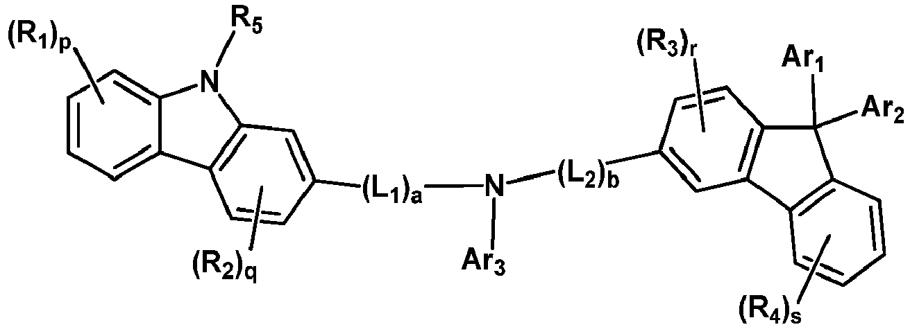 Ar1 and Ar2 are each independently a hydrogen atom, a deuterium atom, a halogen atom, a substituted or unsubstituted alkyl group of 1 to 30 carbon atoms, a substituted or unsubstituted aryl group of 6 to 30 ring-forming carbon atoms, or a substituted or unsubstituted heteroaryl group of 2 to 30 ring-forming carbon atoms, or combined with an adjacent group to form a ring,Ar3 is a substituted or unsubstituted aryl group of 6 to 30 ring-forming carbon atoms, or a substituted or unsubstituted heteroaryl group of 2 to 30 ring-forming carbon atoms,"a" and "b" are each independently 0 or 1,L1 and L2 are each independently a substituted or unsubstituted cycloalkylene group of 3 to 10 ring-forming carbon atoms, a substituted or unsubstituted heterocycloalkylene group of 2 to 10 ring-forming carbon atoms, a substituted or unsubstituted cycloalkenylene group of 3 to 10 ring-forming carbon atoms, a substituted or unsubstituted arylene group of 6 to 30 ring-forming carbon atoms, or a substituted or unsubstituted heteroarylene group of 2 to 60 ring-forming carbon atoms,"p" and "s" are each independently an integer of 0 to 4,"q" and "r" are each independently an integer of 0 to 3, andR1 to R5 are each independently a hydrogen atom, a deuterium atom, a halogen atom, a hydroxyl group, a cyano group, a nitro group, an amino group, a substituted or unsubstituted silyl group, a substituted or unsubstituted oxy group, a substituted or unsubstituted alkyl group of 1 to 60 carbon atoms, a substituted or unsubstituted heterocycloalkyl group of 3 to 60 ring-forming carbon atoms, a substituted or unsubstituted aryl group of 6 to 60 ring-forming carbon atoms, or a substituted or unsubstituted heteroaryl group of 2 to 60 ring-forming carbon atoms.
 - The light emitting diode of any one or more of the preceding claims, wherein the third hole transport layer comprises at least one among compounds in the following Compound Group 2:


- The light emitting diode of any one or more of the preceding claims, wherein the hole transport region further comprises:a fourth hole transport layer disposed between the first hole transport layer and the third hole transport layer and having a refractive index value greater than the first refractive index and less than the third refractive index; anda fifth hole transport layer disposed between the second hole transport layer and the third hole transport layer and having a refractive index value greater than the second refractive index and less than the third refractive index, preferably whereineach of the first hole transport layer and the second hole transport layer comprises an amine compound represented by the following Formula 1,the third hole transport layer comprises a compound represented by the following Formula 2, andeach of the fourth hole transport layer and the fifth hole transport layer comprises the amine compound represented by the following Formula 1 and the compound represented by the following Formula 2:
 Ara to Arc are each independently a substituted or unsubstituted aryl group of 6 to 30 ring-forming carbon atoms, or a substituted or unsubstituted heteroaryl group of 3 to 30 ring-forming carbon atoms,at least two among Ra to Rc are each independently an adamantyl group or a cyclohexyl group, andthe remainder is a hydrogen atom, a deuterium atom, a halogen atom, a cyano group, a substituted or unsubstituted oxy group, a substituted or unsubstituted thio group, a substituted or unsubstituted amine group, or a substituted or unsubstituted alkyl group of 1 to 20 carbon atoms,
 Ar1 and Ar2 are each independently a hydrogen atom, a deuterium atom, a halogen atom, a substituted or unsubstituted alkyl group of 1 to 30 carbon atoms, a substituted or unsubstituted aryl group of 6 to 30 ring-forming carbon atoms, or a substituted or unsubstituted heteroaryl group of 2 to 30 ring-forming carbon atoms, or combined with an adjacent group to form a ring,Ar3 is a substituted or unsubstituted aryl group of 6 to 30 ring-forming carbon atoms, or a substituted or unsubstituted heteroaryl group of 2 to 30 ring-forming carbon atoms,"a" and "b" are each independently 0 or 1,L1 and L2 are each independently a substituted or unsubstituted cycloalkylene group of 3 to 10 ring-forming carbon atoms, a substituted or unsubstituted heterocycloalkylene group of 2 to 10 ring-forming carbon atoms, a substituted or unsubstituted cycloalkenylene group of 3 to 10 ring-forming carbon atoms, a substituted or unsubstituted arylene group of 6 to 30 ring-forming carbon atoms, or a substituted or unsubstituted heteroarylene group of 2 to 60 ring-forming carbon atoms,"p" and "s" are each independently an integer of 0 to 4,"q" and "r" are each independently an integer of 0 to 3, andR1 to R5 are each independently a hydrogen atom, a deuterium atom, a halogen atom, a hydroxyl group, a cyano group, a nitro group, an amino group, a substituted or unsubstituted silyl group, a substituted or unsubstituted oxy group, a substituted or unsubstituted alkyl group of 1 to 60 carbon atoms, a substituted or unsubstituted heterocycloalkyl group of 3 to 60 ring-forming carbon atoms, a substituted or unsubstituted aryl group of 6 to 60 ring-forming carbon atoms, or a substituted or unsubstituted heteroaryl group of 2 to 60 ring-forming carbon atoms; or wherein a thickness of each of the first to fifth hole transport layers is 100 Å to 1,000 Å.
 - A display device, comprising a plurality of light emitting diodes,
wherein each light emitting diode is any one of claims 1 to 14.
Applications Claiming Priority (2)
| Application Number | Priority Date | Filing Date | Title |
|---|---|---|---|
| KR20200007949 | 2020-01-21 | ||
| KR1020200176483A KR102498041B1 (en) | 2020-01-21 | 2020-12-16 | Amine compound, light emitting diode and display device including the same |
Publications (1)
| Publication Number | Publication Date |
|---|---|
| EP3855524A1 true EP3855524A1 (en) | 2021-07-28 |
Family
ID=74191606
Family Applications (1)
| Application Number | Title | Priority Date | Filing Date |
|---|---|---|---|
| EP21152336.0A Pending EP3855524A1 (en) | 2020-01-21 | 2021-01-19 | Light emitting diode and display device including the same |
Country Status (3)
| Country | Link |
|---|---|
| US (1) | US11744147B2 (en) |
| EP (1) | EP3855524A1 (en) |
| CN (1) | CN113224246B (en) |
Cited By (1)
| Publication number | Priority date | Publication date | Assignee | Title |
|---|---|---|---|---|
| EP4174055A1 (en) * | 2021-10-29 | 2023-05-03 | Samsung Display Co., Ltd. | Light emitting device and amine compound for light emitting device |
Families Citing this family (10)
| Publication number | Priority date | Publication date | Assignee | Title |
|---|---|---|---|---|
| JPWO2021260494A1 (en) * | 2020-06-26 | 2021-12-30 | ||
| KR102817317B1 (en) | 2020-07-22 | 2025-06-10 | 삼성디스플레이 주식회사 | Organic light emitting diode |
| US11575087B1 (en) | 2020-12-25 | 2023-02-07 | Idemitsu Kosan Co., Ltd. | Organic electroluminescence device, light emitting device, organic electroluminescence display device and electronic device |
| US12369490B2 (en) | 2021-01-13 | 2025-07-22 | Idemitsu Kosan Co., Ltd. | Organic electroluminescent element, organic electroluminescent display device, and electronic device |
| US12389739B2 (en) | 2021-02-25 | 2025-08-12 | Semiconductor Energy Laboratory Co., Ltd. | Light-emitting device, display device, light-emitting apparatus, electronic device, and lighting device |
| CN116097929A (en) * | 2021-08-30 | 2023-05-09 | 京东方科技集团股份有限公司 | Display substrate and display device |
| JP2025014072A (en) | 2021-10-01 | 2025-01-29 | 出光興産株式会社 | Organic electroluminescence element, organic electroluminescence display device and electronic device |
| JP2025016806A (en) | 2021-10-15 | 2025-02-05 | 出光興産株式会社 | Organic electroluminescence element and electronic device |
| CN118266282A (en) * | 2022-10-28 | 2024-06-28 | 京东方科技集团股份有限公司 | Light-emitting device and preparation method thereof, and display substrate |
| CN117586131A (en) * | 2023-11-30 | 2024-02-23 | 浙江华显光电科技有限公司 | Low refractive index organic compound, OLED (organic light emitting diode) with same and organic light emitting device |
Citations (12)
| Publication number | Priority date | Publication date | Assignee | Title |
|---|---|---|---|---|
| EP2347896A1 (en) | 2008-10-17 | 2011-07-27 | Hitachi Chemical Company, Ltd. | Film having low refractive index and method for producing the same, anti-reflection film and method for producing the same, coating liquid set for film having low refractive index, substrate having microparticle-laminated thin film, and method for producing the same, and optical member |
| WO2012034627A1 (en) | 2010-09-15 | 2012-03-22 | Merck Patent Gmbh | Materials for organic electroluminescent devices |
| WO2014166572A1 (en) | 2013-04-08 | 2014-10-16 | Merck Patent Gmbh | Organic light-emitting device having delayed fluorescence |
| US20160043317A1 (en) | 2014-08-05 | 2016-02-11 | Samsung Display Co., Ltd. | Organic electroluminescent device |
| US20160079542A1 (en) * | 2014-09-09 | 2016-03-17 | Samsung Display Co., Ltd. | Organic electroluminescence device |
| US20160133850A1 (en) | 2014-11-07 | 2016-05-12 | Samsung Display Co., Ltd. | Organic electroluminescent device |
| US20160197277A1 (en) | 2014-07-11 | 2016-07-07 | Idemitsu Kosan Co., Ltd. | Compound, material for organic electroluminescence devices, organic electroluminescence device, and electronic equipment |
| KR20180047421A (en) * | 2016-10-31 | 2018-05-10 | 엘지디스플레이 주식회사 | Organic Light Emitting Diode Display Device |
| KR20180082710A (en) | 2017-01-10 | 2018-07-19 | 삼성디스플레이 주식회사 | Organic electroluminescence device |
| TWI660535B (en) | 2017-03-22 | 2019-05-21 | 財團法人工業技術研究院 | Organic light-emitting device |
| US20190393426A1 (en) | 2017-01-30 | 2019-12-26 | Idemitsu Kosan Co., Ltd. | Organic electroluminescent element and electronic device |
| WO2020050372A1 (en) | 2018-09-07 | 2020-03-12 | 出光興産株式会社 | Organic electroluminescent element and electronic device |
Family Cites Families (25)
| Publication number | Priority date | Publication date | Assignee | Title |
|---|---|---|---|---|
| US4720432A (en) | 1987-02-11 | 1988-01-19 | Eastman Kodak Company | Electroluminescent device with organic luminescent medium |
| US5061569A (en) | 1990-07-26 | 1991-10-29 | Eastman Kodak Company | Electroluminescent device with organic electroluminescent medium |
| JP3556258B2 (en) | 1992-12-18 | 2004-08-18 | 株式会社リコー | Organic thin film EL device having a plurality of carrier injection layers |
| JP2873548B2 (en) | 1995-04-21 | 1999-03-24 | バンドー化学株式会社 | New triphenylamine compounds |
| US6242115B1 (en) | 1997-09-08 | 2001-06-05 | The University Of Southern California | OLEDs containing thermally stable asymmetric charge carrier materials |
| JP3856546B2 (en) | 1997-11-11 | 2006-12-13 | 三井化学株式会社 | Organic electroluminescence device |
| JP4542646B2 (en) | 1998-09-09 | 2010-09-15 | 出光興産株式会社 | Organic electroluminescence device and phenylenediamine derivative |
| JP4573923B2 (en) | 1999-04-27 | 2010-11-04 | 三井化学株式会社 | Amine compounds |
| KR100787425B1 (en) | 2004-11-29 | 2007-12-26 | 삼성에스디아이 주식회사 | Phenylcarbazole compound and organic electroluminescent device using same |
| KR100611756B1 (en) | 2004-06-18 | 2006-08-10 | 삼성에스디아이 주식회사 | Organic electroluminescent device and manufacturing method thereof |
| KR101084197B1 (en) | 2010-02-24 | 2011-11-17 | 삼성모바일디스플레이주식회사 | OLED display and manufacturing method thereof |
| KR101097339B1 (en) | 2010-03-08 | 2011-12-23 | 삼성모바일디스플레이주식회사 | Organic light emitting diode and method for preparing the same |
| EP2638579B1 (en) | 2010-11-09 | 2018-01-24 | Koninklijke Philips N.V. | Organic electroluminescent device |
| US8471463B2 (en) | 2011-08-12 | 2013-06-25 | Canon Kabushiki Kaisha | Organic EL element, and light-emitting apparatus, image-forming apparatus, display apparatus and imaging apparatus using the organic EL element |
| JP6034600B2 (en) | 2012-06-12 | 2016-11-30 | ユー・ディー・シー アイルランド リミテッド | Organic electroluminescence device |
| KR102047279B1 (en) | 2013-01-24 | 2019-11-22 | 삼성디스플레이 주식회사 | Organic light emitting display device and method of manufacturing the same |
| JP2016039187A (en) | 2014-08-05 | 2016-03-22 | 三星ディスプレイ株式會社Samsung Display Co.,Ltd. | Organic electroluminescent element |
| JP2016092297A (en) | 2014-11-07 | 2016-05-23 | 三星ディスプレイ株式會社Samsung Display Co.,Ltd. | Organic electroluminescent element |
| KR101708176B1 (en) | 2015-12-31 | 2017-02-20 | 머티어리얼사이언스 주식회사 | Organic compound and organic electroluminescent device comprising the same |
| US10483479B2 (en) | 2016-03-01 | 2019-11-19 | Pioneer Corporation | Method of manufacturing organic light emitting device and organic light emitting device |
| TW201920343A (en) | 2017-06-21 | 2019-06-01 | 德商麥克專利有限公司 | Materials for electronic devices |
| KR102660941B1 (en) | 2017-11-28 | 2024-04-26 | 삼성디스플레이 주식회사 | Organic electroluminescence device and monoamine compound for organic electroluminescence device |
| JP7465062B2 (en) * | 2018-01-26 | 2024-04-10 | 三星ディスプレイ株式會社 | Organic electroluminescent device and monoamine compound for organic electroluminescent device |
| CN108717941B (en) * | 2018-05-28 | 2020-11-06 | 上海天马有机发光显示技术有限公司 | Organic light-emitting display panel and organic light-emitting display device |
| KR102817317B1 (en) | 2020-07-22 | 2025-06-10 | 삼성디스플레이 주식회사 | Organic light emitting diode |
-
2021
- 2021-01-19 EP EP21152336.0A patent/EP3855524A1/en active Pending
- 2021-01-20 US US17/153,310 patent/US11744147B2/en active Active
- 2021-01-21 CN CN202110081767.1A patent/CN113224246B/en active Active
Patent Citations (12)
| Publication number | Priority date | Publication date | Assignee | Title |
|---|---|---|---|---|
| EP2347896A1 (en) | 2008-10-17 | 2011-07-27 | Hitachi Chemical Company, Ltd. | Film having low refractive index and method for producing the same, anti-reflection film and method for producing the same, coating liquid set for film having low refractive index, substrate having microparticle-laminated thin film, and method for producing the same, and optical member |
| WO2012034627A1 (en) | 2010-09-15 | 2012-03-22 | Merck Patent Gmbh | Materials for organic electroluminescent devices |
| WO2014166572A1 (en) | 2013-04-08 | 2014-10-16 | Merck Patent Gmbh | Organic light-emitting device having delayed fluorescence |
| US20160197277A1 (en) | 2014-07-11 | 2016-07-07 | Idemitsu Kosan Co., Ltd. | Compound, material for organic electroluminescence devices, organic electroluminescence device, and electronic equipment |
| US20160043317A1 (en) | 2014-08-05 | 2016-02-11 | Samsung Display Co., Ltd. | Organic electroluminescent device |
| US20160079542A1 (en) * | 2014-09-09 | 2016-03-17 | Samsung Display Co., Ltd. | Organic electroluminescence device |
| US20160133850A1 (en) | 2014-11-07 | 2016-05-12 | Samsung Display Co., Ltd. | Organic electroluminescent device |
| KR20180047421A (en) * | 2016-10-31 | 2018-05-10 | 엘지디스플레이 주식회사 | Organic Light Emitting Diode Display Device |
| KR20180082710A (en) | 2017-01-10 | 2018-07-19 | 삼성디스플레이 주식회사 | Organic electroluminescence device |
| US20190393426A1 (en) | 2017-01-30 | 2019-12-26 | Idemitsu Kosan Co., Ltd. | Organic electroluminescent element and electronic device |
| TWI660535B (en) | 2017-03-22 | 2019-05-21 | 財團法人工業技術研究院 | Organic light-emitting device |
| WO2020050372A1 (en) | 2018-09-07 | 2020-03-12 | 出光興産株式会社 | Organic electroluminescent element and electronic device |
Non-Patent Citations (3)
| Title |
|---|
| KUMAR G A ET AL: "PHYSICAL AND OPTICAL PROPERTIES OF PHTHALOCYANINE DOPED INORGANIC GLASSES", JOURNAL OF MATERIAL SCIENCE, KLUWER ACADEMIC PUBLISHERS, DORDRECHT, vol. 35, no. 10, 1 May 2000 (2000-05-01), pages 2539 - 2542, XP001006514, ISSN: 0022-2461, DOI: 10.1023/A:1004794424439 * |
| SCHWAB ET AL.: "Efficiency enhancement of top-emitting organic light-emitting diodes using conversion dyes", JOURNAL OF APPLIED PHYSICS, vol. 110, no. 8, 15 October 2011 (2011-10-15), pages 83118-1 - 083118-6, XP012150791, ISSN: 0021-8979, DOI: 10.1063/1.3656452 |
| SCHWAB TOBIAS; THOMSCHKE MICHAEL; HOFMANN SIMONE; FURNO MAURO; LEO KARL; LüSSEM BJöRN: "Efficiency enhancement of top-emitting organic light-emitting diodes using conversion dyes", JOURNAL OF APPLIED PHYSICS, AMERICAN INSTITUTE OF PHYSICS, 2 HUNTINGTON QUADRANGLE, MELVILLE, NY 11747, vol. 110, no. 8, 15 October 2011 (2011-10-15), 2 Huntington Quadrangle, Melville, NY 11747, pages 83118-1 - 083118-6, XP012150791, ISSN: 0021-8979, DOI: 10.1063/1.3656452 |
Cited By (1)
| Publication number | Priority date | Publication date | Assignee | Title |
|---|---|---|---|---|
| EP4174055A1 (en) * | 2021-10-29 | 2023-05-03 | Samsung Display Co., Ltd. | Light emitting device and amine compound for light emitting device |
Also Published As
| Publication number | Publication date |
|---|---|
| US11744147B2 (en) | 2023-08-29 |
| CN113224246A (en) | 2021-08-06 |
| US20210234098A1 (en) | 2021-07-29 |
| CN113224246B (en) | 2026-03-31 |
Similar Documents
| Publication | Publication Date | Title |
|---|---|---|
| US12356795B2 (en) | Light emitting diode and display device including the same | |
| EP3855524A1 (en) | Light emitting diode and display device including the same | |
| KR102656066B1 (en) | Novel amine compounds for organic light-emitting diode and organic light-emitting diode including the same | |
| JP2021014455A (en) | Compound for organic electric element, organic electric element based on the same, and electronic device thereof | |
| KR20230064741A (en) | Organic compound and electroluminescent device comprising the same | |
| KR102316570B1 (en) | An electroluminescent compound and an electroluminescent device comprising the same | |
| KR20210090389A (en) | An electroluminescent compound and an electroluminescent device comprising the same | |
| KR102356004B1 (en) | An electroluminescent compound and an electroluminescent device comprising the same | |
| KR102120917B1 (en) | An electroluminescent compound and an electroluminescent device comprising the same | |
| KR20210048018A (en) | An electroluminescent compound and an electroluminescent device comprising the same | |
| KR102254304B1 (en) | Organic light emitting device | |
| KR20230110447A (en) | Organic compound and electroluminescent device comprising the same | |
| KR20230125405A (en) | Organic compound and electroluminescent device comprising the same | |
| KR20220005264A (en) | An electroluminescent compound and an electroluminescent device comprising the same | |
| KR102899760B1 (en) | Organic compounds and electroluminescent device comprising the same | |
| KR102825694B1 (en) | An electroluminescent compound and an electroluminescent device comprising the same | |
| KR102928137B1 (en) | An electroluminescent compound and an electroluminescent device comprising the same | |
| KR20260045971A (en) | Organic compounds and electroluminescent device comprising the same | |
| KR20250004453A (en) | Organic compounds and electroluminescent device comprising the same | |
| KR20240095545A (en) | Organic compound and electroluminescent device comprising the same | |
| KR20260037986A (en) | Organic compound and electroluminescent device comprising the same | |
| KR20230120146A (en) | An electroluminescent compound and an electroluminescent device comprising the same | |
| KR20220152653A (en) | An electroluminescent compound and an electroluminescent device comprising the same | |
| KR20250034210A (en) | Organic compounds and electroluminescent device comprising the same | |
| KR20250033410A (en) | Organic compounds and electroluminescent device comprising the same |
Legal Events
| Date | Code | Title | Description |
|---|---|---|---|
| PUAI | Public reference made under article 153(3) epc to a published international application that has entered the european phase |
Free format text: ORIGINAL CODE: 0009012 |
|
| STAA | Information on the status of an ep patent application or granted ep patent |
Free format text: STATUS: THE APPLICATION HAS BEEN PUBLISHED |
|
| AK | Designated contracting states |
Kind code of ref document: A1 Designated state(s): AL AT BE BG CH CY CZ DE DK EE ES FI FR GB GR HR HU IE IS IT LI LT LU LV MC MK MT NL NO PL PT RO RS SE SI SK SM TR |
|
| TPAC | Observations filed by third parties |
Free format text: ORIGINAL CODE: EPIDOSNTIPA |
|
| STAA | Information on the status of an ep patent application or granted ep patent |
Free format text: STATUS: REQUEST FOR EXAMINATION WAS MADE |
|
| 17P | Request for examination filed |
Effective date: 20220127 |
|
| RBV | Designated contracting states (corrected) |
Designated state(s): AL AT BE BG CH CY CZ DE DK EE ES FI FR GB GR HR HU IE IS IT LI LT LU LV MC MK MT NL NO PL PT RO RS SE SI SK SM TR |
|
| TPAC | Observations filed by third parties |
Free format text: ORIGINAL CODE: EPIDOSNTIPA |
|
| P01 | Opt-out of the competence of the unified patent court (upc) registered |
Effective date: 20230516 |