EP3855523A1 - Photoelectric converter, photoelectric conversion module, electronic device, and power source module - Google Patents
Photoelectric converter, photoelectric conversion module, electronic device, and power source module Download PDFInfo
- Publication number
- EP3855523A1 EP3855523A1 EP21152355.0A EP21152355A EP3855523A1 EP 3855523 A1 EP3855523 A1 EP 3855523A1 EP 21152355 A EP21152355 A EP 21152355A EP 3855523 A1 EP3855523 A1 EP 3855523A1
- Authority
- EP
- European Patent Office
- Prior art keywords
- photoelectric converter
- photoelectric conversion
- photoelectric
- transport layer
- layer
- Prior art date
- Legal status (The legal status is an assumption and is not a legal conclusion. Google has not performed a legal analysis and makes no representation as to the accuracy of the status listed.)
- Withdrawn
Links
- 238000006243 chemical reaction Methods 0.000 title claims abstract description 187
- 230000005525 hole transport Effects 0.000 claims abstract description 41
- 239000000758 substrate Substances 0.000 claims abstract description 38
- 239000011368 organic material Substances 0.000 claims abstract description 33
- 239000002245 particle Substances 0.000 claims description 57
- XLOMVQKBTHCTTD-UHFFFAOYSA-N Zinc monoxide Chemical compound [Zn]=O XLOMVQKBTHCTTD-UHFFFAOYSA-N 0.000 claims description 35
- 230000005611 electricity Effects 0.000 claims description 35
- 229910044991 metal oxide Inorganic materials 0.000 claims description 32
- 150000004706 metal oxides Chemical class 0.000 claims description 32
- 239000000126 substance Substances 0.000 claims description 28
- 239000011787 zinc oxide Substances 0.000 claims description 17
- -1 amine compound Chemical class 0.000 claims description 13
- 125000004432 carbon atom Chemical group C* 0.000 claims description 13
- 150000001875 compounds Chemical class 0.000 claims description 12
- 238000004770 highest occupied molecular orbital Methods 0.000 claims description 12
- 125000000217 alkyl group Chemical group 0.000 claims description 10
- 239000012789 electroconductive film Substances 0.000 claims description 9
- XOLBLPGZBRYERU-UHFFFAOYSA-N tin dioxide Chemical compound O=[Sn]=O XOLBLPGZBRYERU-UHFFFAOYSA-N 0.000 claims description 9
- XMWRBQBLMFGWIX-UHFFFAOYSA-N C60 fullerene Chemical class C12=C3C(C4=C56)=C7C8=C5C5=C9C%10=C6C6=C4C1=C1C4=C6C6=C%10C%10=C9C9=C%11C5=C8C5=C8C7=C3C3=C7C2=C1C1=C2C4=C6C4=C%10C6=C9C9=C%11C5=C5C8=C3C3=C7C1=C1C2=C4C6=C2C9=C5C3=C12 XMWRBQBLMFGWIX-UHFFFAOYSA-N 0.000 claims description 8
- 229910001887 tin oxide Inorganic materials 0.000 claims description 7
- 229910000476 molybdenum oxide Inorganic materials 0.000 claims description 6
- PQQKPALAQIIWST-UHFFFAOYSA-N oxomolybdenum Chemical compound [Mo]=O PQQKPALAQIIWST-UHFFFAOYSA-N 0.000 claims description 6
- XHCLAFWTIXFWPH-UHFFFAOYSA-N [O-2].[O-2].[O-2].[O-2].[O-2].[V+5].[V+5] Chemical compound [O-2].[O-2].[O-2].[O-2].[O-2].[V+5].[V+5] XHCLAFWTIXFWPH-UHFFFAOYSA-N 0.000 claims description 5
- QGLKJKCYBOYXKC-UHFFFAOYSA-N nonaoxidotritungsten Chemical compound O=[W]1(=O)O[W](=O)(=O)O[W](=O)(=O)O1 QGLKJKCYBOYXKC-UHFFFAOYSA-N 0.000 claims description 5
- 229910001930 tungsten oxide Inorganic materials 0.000 claims description 5
- 229910001935 vanadium oxide Inorganic materials 0.000 claims description 5
- GWEVSGVZZGPLCZ-UHFFFAOYSA-N Titan oxide Chemical compound O=[Ti]=O GWEVSGVZZGPLCZ-UHFFFAOYSA-N 0.000 claims description 4
- 125000003118 aryl group Chemical group 0.000 claims description 4
- OGIDPMRJRNCKJF-UHFFFAOYSA-N titanium oxide Inorganic materials [Ti]=O OGIDPMRJRNCKJF-UHFFFAOYSA-N 0.000 claims description 4
- 229910007157 Si(OH)3 Inorganic materials 0.000 claims description 3
- 125000003178 carboxy group Chemical group [H]OC(*)=O 0.000 claims description 3
- 125000000547 substituted alkyl group Chemical group 0.000 claims description 3
- 239000010410 layer Substances 0.000 description 250
- 239000007788 liquid Substances 0.000 description 42
- 238000002360 preparation method Methods 0.000 description 25
- 239000000463 material Substances 0.000 description 22
- 238000005286 illumination Methods 0.000 description 21
- 239000010409 thin film Substances 0.000 description 21
- 238000010586 diagram Methods 0.000 description 20
- 238000000034 method Methods 0.000 description 19
- 238000010248 power generation Methods 0.000 description 18
- 238000007789 sealing Methods 0.000 description 17
- 230000015572 biosynthetic process Effects 0.000 description 16
- 239000004065 semiconductor Substances 0.000 description 14
- 241000699666 Mus <mouse, genus> Species 0.000 description 13
- 239000010408 film Substances 0.000 description 13
- 239000007789 gas Substances 0.000 description 13
- HEDRZPFGACZZDS-UHFFFAOYSA-N Chloroform Chemical compound ClC(Cl)Cl HEDRZPFGACZZDS-UHFFFAOYSA-N 0.000 description 12
- 230000000052 comparative effect Effects 0.000 description 12
- 239000002105 nanoparticle Substances 0.000 description 12
- 230000004888 barrier function Effects 0.000 description 11
- 239000011342 resin composition Substances 0.000 description 11
- 239000006185 dispersion Substances 0.000 description 10
- 239000012535 impurity Substances 0.000 description 10
- 239000002904 solvent Substances 0.000 description 10
- MVPPADPHJFYWMZ-UHFFFAOYSA-N chlorobenzene Chemical compound ClC1=CC=CC=C1 MVPPADPHJFYWMZ-UHFFFAOYSA-N 0.000 description 8
- LFQSCWFLJHTTHZ-UHFFFAOYSA-N Ethanol Chemical compound CCO LFQSCWFLJHTTHZ-UHFFFAOYSA-N 0.000 description 7
- MCEWYIDBDVPMES-UHFFFAOYSA-N [60]pcbm Chemical compound C123C(C4=C5C6=C7C8=C9C%10=C%11C%12=C%13C%14=C%15C%16=C%17C%18=C(C=%19C=%20C%18=C%18C%16=C%13C%13=C%11C9=C9C7=C(C=%20C9=C%13%18)C(C7=%19)=C96)C6=C%11C%17=C%15C%13=C%15C%14=C%12C%12=C%10C%10=C85)=C9C7=C6C2=C%11C%13=C2C%15=C%12C%10=C4C23C1(CCCC(=O)OC)C1=CC=CC=C1 MCEWYIDBDVPMES-UHFFFAOYSA-N 0.000 description 7
- 230000007423 decrease Effects 0.000 description 7
- 229910052751 metal Inorganic materials 0.000 description 7
- 239000002184 metal Substances 0.000 description 7
- 238000001035 drying Methods 0.000 description 6
- 239000011521 glass Substances 0.000 description 6
- 229920002799 BoPET Polymers 0.000 description 5
- 239000000370 acceptor Substances 0.000 description 5
- 238000011156 evaluation Methods 0.000 description 5
- 238000005259 measurement Methods 0.000 description 5
- 239000000203 mixture Substances 0.000 description 5
- 229920000139 polyethylene terephthalate Polymers 0.000 description 5
- 239000005020 polyethylene terephthalate Substances 0.000 description 5
- 239000012790 adhesive layer Substances 0.000 description 4
- 229910052782 aluminium Inorganic materials 0.000 description 4
- XAGFODPZIPBFFR-UHFFFAOYSA-N aluminium Chemical compound [Al] XAGFODPZIPBFFR-UHFFFAOYSA-N 0.000 description 4
- PNEYBMLMFCGWSK-UHFFFAOYSA-N aluminium oxide Inorganic materials [O-2].[O-2].[O-2].[Al+3].[Al+3] PNEYBMLMFCGWSK-UHFFFAOYSA-N 0.000 description 4
- 238000000137 annealing Methods 0.000 description 4
- 230000005540 biological transmission Effects 0.000 description 4
- PCHJSUWPFVWCPO-UHFFFAOYSA-N gold Chemical compound [Au] PCHJSUWPFVWCPO-UHFFFAOYSA-N 0.000 description 4
- 229910052737 gold Inorganic materials 0.000 description 4
- 239000010931 gold Substances 0.000 description 4
- 229920003023 plastic Polymers 0.000 description 4
- 229920000642 polymer Polymers 0.000 description 4
- 230000008569 process Effects 0.000 description 4
- CSCPPACGZOOCGX-UHFFFAOYSA-N Acetone Chemical compound CC(C)=O CSCPPACGZOOCGX-UHFFFAOYSA-N 0.000 description 3
- YMWUJEATGCHHMB-UHFFFAOYSA-N Dichloromethane Chemical compound ClCCl YMWUJEATGCHHMB-UHFFFAOYSA-N 0.000 description 3
- XEKOWRVHYACXOJ-UHFFFAOYSA-N Ethyl acetate Chemical compound CCOC(C)=O XEKOWRVHYACXOJ-UHFFFAOYSA-N 0.000 description 3
- LYCAIKOWRPUZTN-UHFFFAOYSA-N Ethylene glycol Chemical compound OCCO LYCAIKOWRPUZTN-UHFFFAOYSA-N 0.000 description 3
- OKKJLVBELUTLKV-UHFFFAOYSA-N Methanol Chemical compound OC OKKJLVBELUTLKV-UHFFFAOYSA-N 0.000 description 3
- ZMXDDKWLCZADIW-UHFFFAOYSA-N N,N-Dimethylformamide Chemical compound CN(C)C=O ZMXDDKWLCZADIW-UHFFFAOYSA-N 0.000 description 3
- YXFVVABEGXRONW-UHFFFAOYSA-N Toluene Chemical compound CC1=CC=CC=C1 YXFVVABEGXRONW-UHFFFAOYSA-N 0.000 description 3
- 238000005229 chemical vapour deposition Methods 0.000 description 3
- 229940125782 compound 2 Drugs 0.000 description 3
- 230000001276 controlling effect Effects 0.000 description 3
- 238000007639 printing Methods 0.000 description 3
- 238000004528 spin coating Methods 0.000 description 3
- 238000004544 sputter deposition Methods 0.000 description 3
- 238000004627 transmission electron microscopy Methods 0.000 description 3
- XLYOFNOQVPJJNP-UHFFFAOYSA-N water Substances O XLYOFNOQVPJJNP-UHFFFAOYSA-N 0.000 description 3
- RFFLAFLAYFXFSW-UHFFFAOYSA-N 1,2-dichlorobenzene Chemical compound ClC1=CC=CC=C1Cl RFFLAFLAYFXFSW-UHFFFAOYSA-N 0.000 description 2
- JTPNRXUCIXHOKM-UHFFFAOYSA-N 1-chloronaphthalene Chemical compound C1=CC=C2C(Cl)=CC=CC2=C1 JTPNRXUCIXHOKM-UHFFFAOYSA-N 0.000 description 2
- YEJRWHAVMIAJKC-UHFFFAOYSA-N 4-Butyrolactone Chemical compound O=C1CCCO1 YEJRWHAVMIAJKC-UHFFFAOYSA-N 0.000 description 2
- UJOBWOGCFQCDNV-UHFFFAOYSA-N 9H-carbazole Chemical compound C1=CC=C2C3=CC=CC=C3NC2=C1 UJOBWOGCFQCDNV-UHFFFAOYSA-N 0.000 description 2
- IJGRMHOSHXDMSA-UHFFFAOYSA-N Atomic nitrogen Chemical compound N#N IJGRMHOSHXDMSA-UHFFFAOYSA-N 0.000 description 2
- OKTJSMMVPCPJKN-UHFFFAOYSA-N Carbon Chemical compound [C] OKTJSMMVPCPJKN-UHFFFAOYSA-N 0.000 description 2
- IAZDPXIOMUYVGZ-UHFFFAOYSA-N Dimethylsulphoxide Chemical compound CS(C)=O IAZDPXIOMUYVGZ-UHFFFAOYSA-N 0.000 description 2
- LRHPLDYGYMQRHN-UHFFFAOYSA-N N-Butanol Chemical compound CCCCO LRHPLDYGYMQRHN-UHFFFAOYSA-N 0.000 description 2
- 229920001609 Poly(3,4-ethylenedioxythiophene) Polymers 0.000 description 2
- 239000004698 Polyethylene Substances 0.000 description 2
- 239000004642 Polyimide Substances 0.000 description 2
- 239000004820 Pressure-sensitive adhesive Substances 0.000 description 2
- WYURNTSHIVDZCO-UHFFFAOYSA-N Tetrahydrofuran Chemical compound C1CCOC1 WYURNTSHIVDZCO-UHFFFAOYSA-N 0.000 description 2
- 239000000654 additive Substances 0.000 description 2
- 239000000853 adhesive Substances 0.000 description 2
- 230000001070 adhesive effect Effects 0.000 description 2
- 229920006223 adhesive resin Polymers 0.000 description 2
- 238000005054 agglomeration Methods 0.000 description 2
- 230000002776 aggregation Effects 0.000 description 2
- QVGXLLKOCUKJST-UHFFFAOYSA-N atomic oxygen Chemical compound [O] QVGXLLKOCUKJST-UHFFFAOYSA-N 0.000 description 2
- 229910052799 carbon Inorganic materials 0.000 description 2
- 239000000969 carrier Substances 0.000 description 2
- 239000011248 coating agent Substances 0.000 description 2
- 238000000576 coating method Methods 0.000 description 2
- 229940125904 compound 1 Drugs 0.000 description 2
- BERDEBHAJNAUOM-UHFFFAOYSA-N copper(i) oxide Chemical compound [Cu]O[Cu] BERDEBHAJNAUOM-UHFFFAOYSA-N 0.000 description 2
- 239000002178 crystalline material Substances 0.000 description 2
- 238000006731 degradation reaction Methods 0.000 description 2
- 230000002542 deteriorative effect Effects 0.000 description 2
- 238000009826 distribution Methods 0.000 description 2
- NIHNNTQXNPWCJQ-UHFFFAOYSA-N fluorene Chemical compound C1=CC=C2CC3=CC=CC=C3C2=C1 NIHNNTQXNPWCJQ-UHFFFAOYSA-N 0.000 description 2
- 238000003306 harvesting Methods 0.000 description 2
- 238000010438 heat treatment Methods 0.000 description 2
- 229910003437 indium oxide Inorganic materials 0.000 description 2
- PJXISJQVUVHSOJ-UHFFFAOYSA-N indium(iii) oxide Chemical compound [O-2].[O-2].[O-2].[In+3].[In+3] PJXISJQVUVHSOJ-UHFFFAOYSA-N 0.000 description 2
- 238000009434 installation Methods 0.000 description 2
- 230000031700 light absorption Effects 0.000 description 2
- 238000004519 manufacturing process Methods 0.000 description 2
- 230000007246 mechanism Effects 0.000 description 2
- 229940057867 methyl lactate Drugs 0.000 description 2
- 238000012986 modification Methods 0.000 description 2
- 230000004048 modification Effects 0.000 description 2
- 239000006199 nebulizer Substances 0.000 description 2
- 239000001301 oxygen Substances 0.000 description 2
- 229910052760 oxygen Inorganic materials 0.000 description 2
- 238000005240 physical vapour deposition Methods 0.000 description 2
- 238000009832 plasma treatment Methods 0.000 description 2
- 239000004033 plastic Substances 0.000 description 2
- 229920000301 poly(3-hexylthiophene-2,5-diyl) polymer Polymers 0.000 description 2
- 229920000728 polyester Polymers 0.000 description 2
- 229920000573 polyethylene Polymers 0.000 description 2
- 229920001721 polyimide Polymers 0.000 description 2
- 238000012545 processing Methods 0.000 description 2
- XSCHRSMBECNVNS-UHFFFAOYSA-N quinoxaline Chemical compound N1=CC=NC2=CC=CC=C21 XSCHRSMBECNVNS-UHFFFAOYSA-N 0.000 description 2
- 230000001105 regulatory effect Effects 0.000 description 2
- 230000003746 surface roughness Effects 0.000 description 2
- 238000012546 transfer Methods 0.000 description 2
- 238000001771 vacuum deposition Methods 0.000 description 2
- SCYULBFZEHDVBN-UHFFFAOYSA-N 1,1-Dichloroethane Chemical compound CC(Cl)Cl SCYULBFZEHDVBN-UHFFFAOYSA-N 0.000 description 1
- DKLWRIQKXIBVIS-UHFFFAOYSA-N 1,1-diiodooctane Chemical compound CCCCCCCC(I)I DKLWRIQKXIBVIS-UHFFFAOYSA-N 0.000 description 1
- FNQJDLTXOVEEFB-UHFFFAOYSA-N 1,2,3-benzothiadiazole Chemical compound C1=CC=C2SN=NC2=C1 FNQJDLTXOVEEFB-UHFFFAOYSA-N 0.000 description 1
- RELMFMZEBKVZJC-UHFFFAOYSA-N 1,2,3-trichlorobenzene Chemical compound ClC1=CC=CC(Cl)=C1Cl RELMFMZEBKVZJC-UHFFFAOYSA-N 0.000 description 1
- OCJBOOLMMGQPQU-UHFFFAOYSA-N 1,4-dichlorobenzene Chemical compound ClC1=CC=C(Cl)C=C1 OCJBOOLMMGQPQU-UHFFFAOYSA-N 0.000 description 1
- KZDTZHQLABJVLE-UHFFFAOYSA-N 1,8-diiodooctane Chemical compound ICCCCCCCCI KZDTZHQLABJVLE-UHFFFAOYSA-N 0.000 description 1
- ISPYQTSUDJAMAB-UHFFFAOYSA-N 2-chlorophenol Chemical compound OC1=CC=CC=C1Cl ISPYQTSUDJAMAB-UHFFFAOYSA-N 0.000 description 1
- AWQFNUMHFNEWGS-UHFFFAOYSA-N 2-methylprop-1-ene;styrene Chemical group CC(C)=C.C=CC1=CC=CC=C1 AWQFNUMHFNEWGS-UHFFFAOYSA-N 0.000 description 1
- 239000005964 Acibenzolar-S-methyl Substances 0.000 description 1
- LSNNMFCWUKXFEE-UHFFFAOYSA-M Bisulfite Chemical compound OS([O-])=O LSNNMFCWUKXFEE-UHFFFAOYSA-M 0.000 description 1
- AZSFNTBGCTUQFX-UHFFFAOYSA-N C12=C3C(C4=C5C=6C7=C8C9=C(C%10=6)C6=C%11C=%12C%13=C%14C%11=C9C9=C8C8=C%11C%15=C%16C=%17C(C=%18C%19=C4C7=C8C%15=%18)=C4C7=C8C%15=C%18C%20=C(C=%178)C%16=C8C%11=C9C%14=C8C%20=C%13C%18=C8C9=%12)=C%19C4=C2C7=C2C%15=C8C=4C2=C1C12C3=C5C%10=C3C6=C9C=4C32C1(CCCC(=O)OC)C1=CC=CC=C1 Chemical compound C12=C3C(C4=C5C=6C7=C8C9=C(C%10=6)C6=C%11C=%12C%13=C%14C%11=C9C9=C8C8=C%11C%15=C%16C=%17C(C=%18C%19=C4C7=C8C%15=%18)=C4C7=C8C%15=C%18C%20=C(C=%178)C%16=C8C%11=C9C%14=C8C%20=C%13C%18=C8C9=%12)=C%19C4=C2C7=C2C%15=C8C=4C2=C1C12C3=C5C%10=C3C6=C9C=4C32C1(CCCC(=O)OC)C1=CC=CC=C1 AZSFNTBGCTUQFX-UHFFFAOYSA-N 0.000 description 1
- 239000004215 Carbon black (E152) Substances 0.000 description 1
- 101710200114 Cysteine proteinase inhibitor 10 Proteins 0.000 description 1
- 239000004593 Epoxy Substances 0.000 description 1
- FYYHWMGAXLPEAU-UHFFFAOYSA-N Magnesium Chemical compound [Mg] FYYHWMGAXLPEAU-UHFFFAOYSA-N 0.000 description 1
- 241000699670 Mus sp. Species 0.000 description 1
- SECXISVLQFMRJM-UHFFFAOYSA-N N-Methylpyrrolidone Chemical compound CN1CCCC1=O SECXISVLQFMRJM-UHFFFAOYSA-N 0.000 description 1
- CTQNGGLPUBDAKN-UHFFFAOYSA-N O-Xylene Chemical compound CC1=CC=CC=C1C CTQNGGLPUBDAKN-UHFFFAOYSA-N 0.000 description 1
- 239000004696 Poly ether ether ketone Substances 0.000 description 1
- GXFMEFUBEMESOM-UHFFFAOYSA-N S1CC=C2C1=C1C(=[SiH]2)SC=C1.S1C=CC2=C1C=CC=C2.S2C=CC1=C2C=CC=C1 Chemical compound S1CC=C2C1=C1C(=[SiH]2)SC=C1.S1C=CC2=C1C=CC=C2.S2C=CC1=C2C=CC=C1 GXFMEFUBEMESOM-UHFFFAOYSA-N 0.000 description 1
- 229910020286 SiOxNy Inorganic materials 0.000 description 1
- VYPSYNLAJGMNEJ-UHFFFAOYSA-N Silicium dioxide Chemical compound O=[Si]=O VYPSYNLAJGMNEJ-UHFFFAOYSA-N 0.000 description 1
- XUIMIQQOPSSXEZ-UHFFFAOYSA-N Silicon Chemical compound [Si] XUIMIQQOPSSXEZ-UHFFFAOYSA-N 0.000 description 1
- BQCADISMDOOEFD-UHFFFAOYSA-N Silver Chemical compound [Ag] BQCADISMDOOEFD-UHFFFAOYSA-N 0.000 description 1
- YTPLMLYBLZKORZ-UHFFFAOYSA-N Thiophene Chemical compound C=1C=CSC=1 YTPLMLYBLZKORZ-UHFFFAOYSA-N 0.000 description 1
- 238000010521 absorption reaction Methods 0.000 description 1
- 230000001133 acceleration Effects 0.000 description 1
- 239000002253 acid Substances 0.000 description 1
- NIXOWILDQLNWCW-UHFFFAOYSA-N acrylic acid group Chemical group C(C=C)(=O)O NIXOWILDQLNWCW-UHFFFAOYSA-N 0.000 description 1
- 229910045601 alloy Inorganic materials 0.000 description 1
- 239000000956 alloy Substances 0.000 description 1
- 239000004411 aluminium Substances 0.000 description 1
- 239000012300 argon atmosphere Substances 0.000 description 1
- 150000004982 aromatic amines Chemical class 0.000 description 1
- 239000012298 atmosphere Substances 0.000 description 1
- 238000005452 bending Methods 0.000 description 1
- 238000004364 calculation method Methods 0.000 description 1
- 239000003990 capacitor Substances 0.000 description 1
- 230000015556 catabolic process Effects 0.000 description 1
- 239000003054 catalyst Substances 0.000 description 1
- 229940126214 compound 3 Drugs 0.000 description 1
- 229920000547 conjugated polymer Polymers 0.000 description 1
- 239000000470 constituent Substances 0.000 description 1
- 229910052593 corundum Inorganic materials 0.000 description 1
- 230000008878 coupling Effects 0.000 description 1
- 238000010168 coupling process Methods 0.000 description 1
- 238000005859 coupling reaction Methods 0.000 description 1
- 239000013078 crystal Substances 0.000 description 1
- 229910021419 crystalline silicon Inorganic materials 0.000 description 1
- 238000005034 decoration Methods 0.000 description 1
- 230000007812 deficiency Effects 0.000 description 1
- 230000001419 dependent effect Effects 0.000 description 1
- 238000000151 deposition Methods 0.000 description 1
- 230000008021 deposition Effects 0.000 description 1
- 230000006866 deterioration Effects 0.000 description 1
- 229940117389 dichlorobenzene Drugs 0.000 description 1
- 238000007607 die coating method Methods 0.000 description 1
- 238000009792 diffusion process Methods 0.000 description 1
- VLNBQUAHERCLKT-UHFFFAOYSA-N dimethylamino benzoate Chemical compound CN(C)OC(=O)C1=CC=CC=C1 VLNBQUAHERCLKT-UHFFFAOYSA-N 0.000 description 1
- 238000007598 dipping method Methods 0.000 description 1
- 230000005684 electric field Effects 0.000 description 1
- 238000005516 engineering process Methods 0.000 description 1
- 239000005038 ethylene vinyl acetate Substances 0.000 description 1
- 229920002313 fluoropolymer Polymers 0.000 description 1
- 229910003472 fullerene Inorganic materials 0.000 description 1
- 238000013007 heat curing Methods 0.000 description 1
- 125000005842 heteroatom Chemical group 0.000 description 1
- 229930195733 hydrocarbon Natural products 0.000 description 1
- 150000002430 hydrocarbons Chemical class 0.000 description 1
- 150000003949 imides Chemical class 0.000 description 1
- 239000011261 inert gas Substances 0.000 description 1
- 150000002484 inorganic compounds Chemical class 0.000 description 1
- 229910010272 inorganic material Inorganic materials 0.000 description 1
- 238000011835 investigation Methods 0.000 description 1
- 229910052749 magnesium Inorganic materials 0.000 description 1
- 239000011777 magnesium Substances 0.000 description 1
- SJCKRGFTWFGHGZ-UHFFFAOYSA-N magnesium silver Chemical compound [Mg].[Ag] SJCKRGFTWFGHGZ-UHFFFAOYSA-N 0.000 description 1
- 230000036244 malformation Effects 0.000 description 1
- 150000002739 metals Chemical class 0.000 description 1
- 238000002156 mixing Methods 0.000 description 1
- 238000001451 molecular beam epitaxy Methods 0.000 description 1
- 238000004776 molecular orbital Methods 0.000 description 1
- 229910000480 nickel oxide Inorganic materials 0.000 description 1
- 229910052757 nitrogen Inorganic materials 0.000 description 1
- WKVAXZCSIOTXBT-UHFFFAOYSA-N octane-1,1-dithiol Chemical compound CCCCCCCC(S)S WKVAXZCSIOTXBT-UHFFFAOYSA-N 0.000 description 1
- 150000002894 organic compounds Chemical class 0.000 description 1
- 239000003960 organic solvent Substances 0.000 description 1
- GNRSAWUEBMWBQH-UHFFFAOYSA-N oxonickel Chemical compound [Ni]=O GNRSAWUEBMWBQH-UHFFFAOYSA-N 0.000 description 1
- 230000002093 peripheral effect Effects 0.000 description 1
- 239000012466 permeate Substances 0.000 description 1
- 125000002080 perylenyl group Chemical group C1(=CC=C2C=CC=C3C4=CC=CC5=CC=CC(C1=C23)=C45)* 0.000 description 1
- CSHWQDPOILHKBI-UHFFFAOYSA-N peryrene Natural products C1=CC(C2=CC=CC=3C2=C2C=CC=3)=C3C2=CC=CC3=C1 CSHWQDPOILHKBI-UHFFFAOYSA-N 0.000 description 1
- 108091008695 photoreceptors Proteins 0.000 description 1
- IEQIEDJGQAUEQZ-UHFFFAOYSA-N phthalocyanine Chemical compound N1C(N=C2C3=CC=CC=C3C(N=C3C4=CC=CC=C4C(=N4)N3)=N2)=C(C=CC=C2)C2=C1N=C1C2=CC=CC=C2C4=N1 IEQIEDJGQAUEQZ-UHFFFAOYSA-N 0.000 description 1
- 229920001200 poly(ethylene-vinyl acetate) Polymers 0.000 description 1
- 229920000052 poly(p-xylylene) Polymers 0.000 description 1
- 229920002492 poly(sulfone) Polymers 0.000 description 1
- 229920000515 polycarbonate Polymers 0.000 description 1
- 239000004417 polycarbonate Substances 0.000 description 1
- 229920001225 polyester resin Polymers 0.000 description 1
- 229920002530 polyetherether ketone Polymers 0.000 description 1
- 229920001296 polysiloxane Polymers 0.000 description 1
- 150000004032 porphyrins Chemical class 0.000 description 1
- 239000000047 product Substances 0.000 description 1
- 238000005546 reactive sputtering Methods 0.000 description 1
- 238000001350 scanning transmission electron microscopy Methods 0.000 description 1
- 238000007650 screen-printing Methods 0.000 description 1
- 229910052710 silicon Inorganic materials 0.000 description 1
- 239000010703 silicon Substances 0.000 description 1
- 229910052814 silicon oxide Inorganic materials 0.000 description 1
- 229910052709 silver Inorganic materials 0.000 description 1
- 239000004332 silver Substances 0.000 description 1
- 238000003980 solgel method Methods 0.000 description 1
- 238000004611 spectroscopical analysis Methods 0.000 description 1
- 238000005507 spraying Methods 0.000 description 1
- YLQBMQCUIZJEEH-UHFFFAOYSA-N tetrahydrofuran Natural products C=1C=COC=1 YLQBMQCUIZJEEH-UHFFFAOYSA-N 0.000 description 1
- 238000002230 thermal chemical vapour deposition Methods 0.000 description 1
- 229920001169 thermoplastic Polymers 0.000 description 1
- 229920002803 thermoplastic polyurethane Polymers 0.000 description 1
- 229920005992 thermoplastic resin Polymers 0.000 description 1
- 229920001187 thermosetting polymer Polymers 0.000 description 1
- 239000004416 thermosoftening plastic Substances 0.000 description 1
- VJYJJHQEVLEOFL-UHFFFAOYSA-N thieno[3,2-b]thiophene Chemical compound S1C=CC2=C1C=CS2 VJYJJHQEVLEOFL-UHFFFAOYSA-N 0.000 description 1
- YJVLWFXZVBOFRZ-UHFFFAOYSA-N titanium zinc Chemical compound [Ti].[Zn] YJVLWFXZVBOFRZ-UHFFFAOYSA-N 0.000 description 1
- 230000026683 transduction Effects 0.000 description 1
- 238000010361 transduction Methods 0.000 description 1
- 230000000007 visual effect Effects 0.000 description 1
- 210000000707 wrist Anatomy 0.000 description 1
- 239000008096 xylene Substances 0.000 description 1
- 229910001845 yogo sapphire Inorganic materials 0.000 description 1
Images




Classifications
-
- H—ELECTRICITY
- H10—SEMICONDUCTOR DEVICES; ELECTRIC SOLID-STATE DEVICES NOT OTHERWISE PROVIDED FOR
- H10K—ORGANIC ELECTRIC SOLID-STATE DEVICES
- H10K30/00—Organic devices sensitive to infrared radiation, light, electromagnetic radiation of shorter wavelength or corpuscular radiation
- H10K30/10—Organic devices sensitive to infrared radiation, light, electromagnetic radiation of shorter wavelength or corpuscular radiation comprising heterojunctions between organic semiconductors and inorganic semiconductors
- H10K30/15—Sensitised wide-bandgap semiconductor devices, e.g. dye-sensitised TiO2
- H10K30/152—Sensitised wide-bandgap semiconductor devices, e.g. dye-sensitised TiO2 the wide bandgap semiconductor comprising zinc oxide, e.g. ZnO
-
- H—ELECTRICITY
- H10—SEMICONDUCTOR DEVICES; ELECTRIC SOLID-STATE DEVICES NOT OTHERWISE PROVIDED FOR
- H10K—ORGANIC ELECTRIC SOLID-STATE DEVICES
- H10K30/00—Organic devices sensitive to infrared radiation, light, electromagnetic radiation of shorter wavelength or corpuscular radiation
- H10K30/10—Organic devices sensitive to infrared radiation, light, electromagnetic radiation of shorter wavelength or corpuscular radiation comprising heterojunctions between organic semiconductors and inorganic semiconductors
- H10K30/15—Sensitised wide-bandgap semiconductor devices, e.g. dye-sensitised TiO2
- H10K30/151—Sensitised wide-bandgap semiconductor devices, e.g. dye-sensitised TiO2 the wide bandgap semiconductor comprising titanium oxide, e.g. TiO2
-
- H—ELECTRICITY
- H10—SEMICONDUCTOR DEVICES; ELECTRIC SOLID-STATE DEVICES NOT OTHERWISE PROVIDED FOR
- H10K—ORGANIC ELECTRIC SOLID-STATE DEVICES
- H10K30/00—Organic devices sensitive to infrared radiation, light, electromagnetic radiation of shorter wavelength or corpuscular radiation
- H10K30/30—Organic devices sensitive to infrared radiation, light, electromagnetic radiation of shorter wavelength or corpuscular radiation comprising bulk heterojunctions, e.g. interpenetrating networks of donor and acceptor material domains
-
- H—ELECTRICITY
- H10—SEMICONDUCTOR DEVICES; ELECTRIC SOLID-STATE DEVICES NOT OTHERWISE PROVIDED FOR
- H10K—ORGANIC ELECTRIC SOLID-STATE DEVICES
- H10K30/00—Organic devices sensitive to infrared radiation, light, electromagnetic radiation of shorter wavelength or corpuscular radiation
- H10K30/80—Constructional details
- H10K30/88—Passivation; Containers; Encapsulations
-
- H—ELECTRICITY
- H10—SEMICONDUCTOR DEVICES; ELECTRIC SOLID-STATE DEVICES NOT OTHERWISE PROVIDED FOR
- H10K—ORGANIC ELECTRIC SOLID-STATE DEVICES
- H10K39/00—Integrated devices, or assemblies of multiple devices, comprising at least one organic radiation-sensitive element covered by group H10K30/00
- H10K39/10—Organic photovoltaic [PV] modules; Arrays of single organic PV cells
-
- Y—GENERAL TAGGING OF NEW TECHNOLOGICAL DEVELOPMENTS; GENERAL TAGGING OF CROSS-SECTIONAL TECHNOLOGIES SPANNING OVER SEVERAL SECTIONS OF THE IPC; TECHNICAL SUBJECTS COVERED BY FORMER USPC CROSS-REFERENCE ART COLLECTIONS [XRACs] AND DIGESTS
- Y02—TECHNOLOGIES OR APPLICATIONS FOR MITIGATION OR ADAPTATION AGAINST CLIMATE CHANGE
- Y02E—REDUCTION OF GREENHOUSE GAS [GHG] EMISSIONS, RELATED TO ENERGY GENERATION, TRANSMISSION OR DISTRIBUTION
- Y02E10/00—Energy generation through renewable energy sources
- Y02E10/50—Photovoltaic [PV] energy
- Y02E10/549—Organic PV cells
Definitions
- the present disclosure relates to a photoelectric converter, a photoelectric conversion module, an electronic device, and a power source module.
- IOT Internet of Things
- sensors need to be connected to all kinds of things to acquire data and power supplies to operate sensors; it is, however, not practical to wire many sensors and use many rechargeable batteries.
- Energy harvesting elements for power source are expected to reduce the burden on the environment, which is a great concern of society.
- photoelectric converters are appealing because they can generate electricity anywhere upon application of light.
- Flexible photoelectric converters in particular, are required to be highly efficient. They are expected to be traceable to curved surfaces and applicable to wearable devices. Feasibility on these applications was discussed and reported in Applied Physics letters 108,253301 (published in 2016 ) and Japanese Journal of Applied Physics 54,071602 (published in 2015 ).
- Organic thin film solar cells are expected to be highly efficient and flexible energy harvesting elements.
- One example of such elements is a photoelectric converter having a transparent substrate film as a substrate, which has been proposed in JP-2014-220333-A1 .
- a housing for mobile electronic device has been proposed in JP-2016-208568-A1 which includes a solar cell module to efficiently generate electricity with a mobile electronic device even when the output voltage of the solar cell module lowers.
- Its attributes are that the decrease of the voltage at the open-circuit voltage is 0.2 V or less when the irradiance lowers from 100 to 1 mW/cm 2 in the relationship between the illuminance and the open-circuit voltage, and the open-circuit voltage is 0.55 V or more at an irradiance of 1.0 W/cm 2 , when the module is measured with a solar simulator under conditions of an airmass (AM) of 1.5 and a temperature of the solar cell module of 25 degrees C with a light entering direction perpendicular to the cell.
- AM airmass
- a photoelectric converter which achieves excellent photoelectric conversion even in low illumination environment in comparison with a high illumination environment.
- image forming, recording, printing, modeling, etc. in the present disclosure represent the same meaning, unless otherwise specified.
- first layer may be in direct contact with a portion or all of the second layer, or there may be one or more intervening layers between the first and second layer, with the second layer being closer to the substrate than the first layer.
- L represents a density ( ⁇ A/cm 2 ) of current leakage at an illuminance of 200 lux and J ph represents a density ( ⁇ A/cm 2 ) of photocurrent at an illuminance of 200 lux.
- photoelectric converter means an element that converts light energy into electric energy or the other way round and includes a solar cell and a photodiode.
- An organic thin film solar cells as an example of the photoelectric converter can be readily made flexible in comparison with an inorganic solar cell, which uses an inorganic crystalline material such as crystal silicon; it is, however, necessary to make the photoelectric conversion layer in an organic thin film solar cell thinner to achieve sufficient attributes because the photoelectric conversion layer is composed of an organic material having a smaller diffusion length of a carrier than an inorganic crystalline material.
- the average thickness of a photoelectric conversion layer made of organic materials is in general around several hundred nanometers. This average thickness is extremely thinner than that of a crystalline silicon solar cell, which is an order of micro meter; it is necessary to secure a uniform thickness of such a thin photoelectric conversion layer when it is formed by a solution process in particular.
- the solution process is used in general to form layers including the photoelectric conversion layer because the process is cost effective.
- the electron transport layer and the hole transport layer contact each other and moreover, the first electrode and the second electrode directly contact each other; the current is leaked from portions having a low resistance.
- Such current leakage damages the attributes of the photoelectric conversion of the organic thin film solar cell. What impact this leakage has on the attributes of photoelectric conversion is known to be dependent on the amount of light entering into an organic thin film solar cell; the attributes of photoelectric conversion deteriorate as the amount of light decreases.
- the attributes of a photoelectric converter including an organic thin film solar cell can be evaluated by the following three parameters: Jsc, the density (A/cm 2 ) of short circuit current in which the photoelectric converter is short-circuited; Voc (V) of open-circuit voltage of a photoelectric converter at an open state; and FF, the curve factor of voltage-current curve.
- Jsc the density (A/cm 2 ) of short circuit current in which the photoelectric converter is short-circuited
- Voc (V) of open-circuit voltage of a photoelectric converter at an open state
- FF the curve factor of voltage-current curve.
- the energy conversion efficiency ⁇ against the incident light energy Pin (W/cm 2 ) is represented by the following equation (2).
- ⁇ J SC ⁇ V OC X FF / P in
- JP-2016-208568-A1 regulates the condition for the open-circuit voltage value of a photoelectric converter capable of efficiently generating electricity without a significant drop of the output power in a low illumination; it is, however, just a limitation on the voltage supplied to a photoelectric converter to operate a mobile device. There is no suggestion or discussion about the mechanism of the attributes of a photoelectric converter deteriorating in an environment of a low illumination or what factor should be controlled to reduce the deterioration.
- an organic thin film solar cell as an example of the photoelectric converter is required to be thin in principle.
- Such a thin film causes a drawback such as current leakage.
- This current leakage causes a problem of a drop of the output power in particular in an low illumination environment such as indoor light.
- the present inventors have formulated a solution to the problem, which is controlling the relative ratio (ratio of current leakage) of the density of current leakage to the density of photocurrent.
- illuminance is used to indicate the amount of light in general
- illuminance is regulated in the present disclosure.
- reference illuminance the reference of minimum illuminance in each environment is regulated in JIS Z 9110:2010 format. Normal visual operation in an ordinary manufacturing factory requires at least 500 lux and other types of operations at a warehouse require at least 200 lux.
- 1 SUN as the reference sunlight is about 100,000 lux and known to be by several hundreds to several thousands larger than the illuminance in an indoor environment.
- the present inventors have acquired the knowledge that the photoelectric conversion of a photoelectric converter deteriorate in an environment of low illumination such as indoor environment when the relative ratio of the density of the current leakage to the density of photocurrent surpasses a certain level.
- the present inventors have found that the density of the current leakage is necessary to decrease to obtain a photoelectric converter having a high photoelectric conversion in an environment of low illumination. The present disclosure was thus made.
- L represents a density ( ⁇ A/cm 2 ) of current leakage at an illuminance of 200 lux and J ph represents a density ( ⁇ A/cm 2 ) of photocurrent density at an illuminance of 200 lux.
- the device evaluation and the current leakage ratio P L are obtained in the following manner.
- the current-voltage attribute is measured changing the illuminance of light to which a device is exposed with a source meter capable of measuring the density of short circuit current and the open-circuit voltage of a target photoelectric converter in an arbitrary illumination. It is preferable to use the same light source regardless of illuminance, yet it is possible to use another illumination when using the same light source is difficult as long as the difference in the color temperatures between the two illuminations is within an absolute value of 200 K.
- L represents a density ( ⁇ A/cm 2 ) of current leakage at an illuminance of 200 lux and J ph represents a density ( ⁇ A/cm 2 ) of photocurrent at an illuminance of 200 lux.
- the density L ( ⁇ A/cm 2 ) of current leakage at an illuminace of 200 lux can be obtained by assigning the values of the density Jsc ( ⁇ A/cm 2 ) of short circuit current and the open-circuit voltage Voc (V) per cell obtained at the measurements at an illuminance of 200 lux into the following equation (3).
- L J ph ⁇ J 0 exp q V oc nkT ⁇ 1
- J ph represents the density ( ⁇ A/cm 2 ) of photocurrent.
- Jo represents the density ( ⁇ A/cm 2 ) of dark current
- n represents ideality factor
- T represents the temperature (K) of a device.
- Voc V OC_mod / N mod
- Jo and n in the equation (3) are values calculated from V OC - 1n(J ph ) plotting obtained by measurements at three or more points arbitrarily-selected from 2,000 to 20,000 lux realized at the illumination mentioned above.
- FIG. 2 is a graph illustrating an example of plotting Voc - 1n(J ph ).
- the plots can be approximate to a straight line when the density of current leakage mentioned above is sufficiently small.
- n the decline of the regression line obtained by the least squares method
- the intercept against the 1n(J ph ) axis is defined as 1n(J O ) regarding the points corresponding to the measurements at the three or more points
- n can be obtained from the following equation (5) and J O can be obtained from the axis intercept.
- the coefficient of determination of the regression line is preferably 0.99 or greater.
- n qm kT
- n normally ranges from 1 to 2.
- n surpasses 2 or J O calculated by the method described above surpasses 0.01 ( ⁇ A/cm 2 )
- the ratio P L of current leakage cannot be correctly calculated by the method mentioned above because the current leakage is extremely large.
- the current leakage ratio in this case is at least above 0.95.
- the density of current leakage is regarded as 0 ( ⁇ A/cm 2 ).
- the way or condition of preparing the photoelectric converter satisfying the requisite of the ratio P L of current leakage of 0.95 or less is not particularly limited and can be suitably selected to suit to a particular application. It includes, for example, the following (1) to (4).
- the substrate is transparent and flexible film or glass which is not flexible but flat.
- the film include, but are not limited to, polyester such as polyethylene terephthalate, polycarbonate, polyimide, polymethyhlmethacrylate, polysulfone, and polyetheretherketone.
- the substrate includes a thin film glass having an average thickness of 200 ⁇ m or less.
- polyester, polyimide, and thin-film glass are preferable because they are readily and cost-effectively manufactured.
- a plastic substrate it is preferable to provide it with a gas barrier layer.
- a gas barrier is a layer for preventing transmission of vapor oxygen.
- a gas barrier having such a function is not particularly limited and can be suitably selected to suit to a particular application.
- a specific example is a plastic substrate covered with aluminum.
- the first electrode is mainly composed of a transparent electroconductive film.
- the first electrode may have a structure of a transparent electroconductive film, a thin metal film layer, and a transparent electroconductive film laminated in this order.
- the same or different materials can be used for the transparent electroconductive films sandwiching the thin metal film.
- the material for use in the transparent electroconductive film include, but are not limited to, tin-doped indium oxide (ITO), zinc-doped indium oxide (IZO), zinc oxide (ZnO), aluminium-doped zinc oxide (AZO), gallium-doped zinc oxide (GZO), and tin oxide (S n O 2 ).
- ITO tin-doped indium oxide
- IZO zinc-doped indium oxide
- ZnO zinc oxide
- AZO aluminium-doped zinc oxide
- GZO gallium-doped zinc oxide
- S n O 2 tin oxide
- the average thickness of the transparent electroconductive film is preferably 30 nm or greater and more preferably from 40 to 150 nm.
- the transparent electrode preferably has a sheet resistance of 50 ⁇ / ⁇ or less, more preferably 30 ⁇ / ⁇ or less, and furthermore preferably 20 ⁇ / ⁇ or less.
- the transparent electrode preferably has a high level of transparency. Its transparency is preferably 60 percent or higher and more preferably 70 percent or higher.
- the upper limit is not particularly limited and can be suitably selected to suit to a particular application; 90 percent or less is preferable.
- the electron transport layer is formed on or overlying the first electrode.
- the electron transport layer preferably contains metal oxide particles.
- the layer can be formed by applying a liquid dispersion of the metal oxide particles followed by drying.
- the metal oxide particles preferably have an n-type semiconductor property. Particles of zinc oxide, titanium oxide, and tin oxide are preferable.
- the metal oxide particle may be doped with other metals.
- metal oxide for use in the electron transport layer include, but are not limited to, zinc oxide, aluminium-doped zinc oxide, gallium-doped zinc oxide, titanium oxide, and tin oxide.
- the average particle diameter (D) of the nano-particulate metal oxide particles is preferably from 1 to 50 nm and more preferably from 5 to 20 nm.
- the average thickness of the electron transport layer is preferably from 10 to 60 nm and more preferably from 15 to 40 nm.
- the average particle diameter (D) of the metal oxide particles can be measured in the following manner.
- a solution of the metal oxide particle is moved to a glass nebulizer with a micro pipette.
- the solution is sprayed from the nebulizer to a grid with collodion film for transmission electron microscopy (TEM).
- TEM transmission electron microscopy
- the grid is deposited with carbon using physical vapor deposition (PVD) method to acquire images of metal oxide particles with an electron microscope.
- PVD physical vapor deposition
- the cross sectional surface of the photoelectric converter is observed with a scanning TEM. Particles are recognized with image processing followed by measuring the particle diameter of the metal oxide particles. The particle size distribution can be measured by laser diffraction/scattering. The method of cross-sectional surface exposure, observation with TEM, and measuring of particle size distribution are already well-known.
- the particle diameter of each of at least randomly selected hundred metal oxide particles is measured and averaged to obtain the average particle diameter of the metal oxide particles.
- the electron transport layer preferably has a structure of a first electron transport layer containing the metal oxide particles and a second electron transport layer between the first electron transport layer and the photoelectric conversion layer.
- the second electron transport layer preferably contains an amine compound represented by the following Chemical Formula (4).
- R 4 and R 5 each, independently substituted or non-substituted alkyl groups having 1 to 4 carbon atoms.
- X represents a divalent aromatic group having 6 to 14 carbon atoms or an alkyl group having 1 to 4 carbon atoms, R 4 and R 5 can share a linkage to form a ring.
- the photoelectric conversion layer is formed on or overlying the electron transport layer.
- the photoelectric conversion layer contains two or more types of organic materials and may contain furthermore optionally other components.
- One of the organic materials of the two or more types of organic materials contained in the photoelectric conversion layer is an electron donor and the others are electron acceptors.
- the electron donor is also referred to as a p-type organic semiconductor material and the electron acceptor is referred to as an n-type organic material.
- the photoelectric conversion layer preferably has a bulk hetero structure containing a mixture of these materials.
- the type of the electron donor used is not particularly limited and can be suitably selected to suit to a particular application.
- the electron donor is preferably a ⁇ -electron conjugated compound having a highest occupied molecular orbital (HOMO) level of from 5.1 to 5.5 eV.
- HOMO highest occupied molecular orbital
- conjugated polymers obtained by coupling aromatic series derivatives such as thiophen, fluorene, carbazole, thienothiophene, benzodithiophene dithienosilole, quinoxaline, and benzothiadiazole, and porphyrin and phthalocyanine, which are conjugated compounds having clearly identified low molecular weights. They also include organic materials such as donor-acceptor linking materials having an electron donating portion and an electron accepting portion in the molecule.
- the materials for electron donor made of low molecular weight conjugated compounds having a number average molecular weight of 10,000 or less are more preferable.
- the number average molecular weight is more preferably 5,000 or less.
- the one of the organic materials of the two or more types of organic materials contained in the photoelectric conversion layer include, but are not limited to, compounds represented by the following Chemical Formula (1).
- the electron donor having a highest occupied molecular orbital (HOMO) level of from 5.1 to 5.5 eV and a number average molecular weight of 10,000 or less include, but are not limited to, the compounds represented by the following Chemical Formula (1).
- R 1 represents an alkyl group having 2 to 8 carbon atoms.
- n represents an integer of from 1 to 2.
- X represents one of the following Chemical Formula (2) and the following Chemical Formula (3).
- R 2 and R 3 each, independently represent linear or branched alkyl groups.
- the linear or branched alkyl group preferably has 2 to 30 carbon atoms.
- the type of electron acceptor organic material as the other organic material mentioned above is not particularly limited and can be suitably selected to suit to a particular application. It is preferably a ⁇ electron conjugated compound having a lowest occupied molecular orbital (LOMO) level of from 3.5 to 4.5 eV.
- LOMO lowest occupied molecular orbital
- Example of the other organic material are electron acceptors (N-type semiconductor) below. Specific examples include, but are not limited to, fullerene or its derivatives, naphthalene tetracarboxylic acid imide derivatives, and perylene teracarboxylic acid imide derivatives. Of these, fullerene derivatives are more preferable.
- fullerene derivatives include, but are not limited to, C60, phenyl-C61-methyl lactate (fullerene derivatives referred to as PCBM, [60]PCBM, or PC61BM in documents), C70, phenyl-C-71-methyl lactate (fullerene derivatives referred to as PCBM, [70]PCBM, or PC71BM in documents), and fullerene derivatives mentioned in the web site of DAIKIN INDUSTRIES, LTD.
- the average thickness of the photoelectric conversion layer is preferably from 50 to 400 nm and more preferably from 60 to 250 nm.
- An average thickness of 50 nm or greater effectively prevents a problem of insufficient production of carriers owing to deficiency of light absorption by the photoelectric conversion layer.
- An average thickness of 400 nm or less effectively prevents the degradation of transport efficiency of carriers produced by light absorption
- the present inventors have found that the relationship between the thicknesses of the electron transport layer and the photoelectric conversion layer have an great impact on reducing the ratio of current leakage.
- the average particle diameter of the metal oxide particles in the electron transport layer is defined as D and the average thickness of the photoelectric conversion layer is defined as T, the following relationship is satisfied: 7.0 ⁇ T/D.
- T/D When T/D is less than 7.0, the probability of the contact between the metal oxide particles and the hole transport layer increases, thereby increasing the density of current leakage; it is, however, possible to reduce the density of current leakage by increasing the average thickness of the photoelectric conversion layer by 7 times or more as large as the average particle diameter of the metal oxide particles.
- a ratio T/D of 10 or more significantly decreases the probability of the contact between the metal oxide particles and the hole transport layer and furthermore decreases the density of current leakage.
- the average thickness T of the photoelectric conversion layer can be measured in the following manner.
- a photoelectric conversion layer is applied onto a substrate and thereafter arbitrarily selected nine sites of the film are wiped with a solvent.
- the steps at the nine wiped sites are measured with DEKTAK manufactured by Bruker Corporation.
- the average of the measurements is defined as the average thickness T of the photoelectric conversion layer.
- the cross sectional surface is observed with scanning electron microscope (SEM) or TEM to obtain the average thickness of the photoelectric conversion layer.
- the organic material it is possible to sequentially apply the organic material to form a planar junction interface; it is, however, preferable to form a bulk heterojunction formed by three-dimensionally mixing the organic materials to increase the junction interface area.
- a material highly soluble in a solvent is dissolved in a solvent to prepare a liquid mixture of each organic material in a form of molecule. After the liquid mixture is applied, the resulting material is dried followed by removing the solvent to form a bulk heterojunction. Optionally, this junction may be heated to optimize the agglomeration state of each semiconductor.
- a liquid dispersion is prepared in which the organic material is dissolved in a solvent and then the liquid dispersion is applied to form a mixture layer.
- this mixture layer may be heated to optimize the agglomeration state of each semiconductor.
- Thin film of the organic material can be formed by methods such as spin coating, blade coating, slid die coating, screen printing, bar coater application, mold application, print transfer method, dip drawing-up method, inkjet method, spraying method, and vacuum deposition method. Of these, a suitable method can be selected to control the thickness and arrangement to suit to attributes of thin film of organic material to be prepared.
- the content here means the mass of the P-type semiconductor material having a structure represented by the Chemical Formula (1) illustrated above and the N-type semiconductor material to the volume of a solution containing the P-type semiconductor material having a structure represented by the Chemical Formula (1) illustrated above, the N-type semiconductor material, and the solvent. Such a content makes it easy to prepare a uniform photoelectric conversion layer.
- Prepared photoelectric conversion layers may be subjected to annealing with a reduced pressure or in an inert gas atmosphere (nitrogen, argon atmosphere) to remove the solvent.
- the temperature during annealing is preferably from 40 to 300 degrees C and more preferably from 50 to 150 degrees C.
- the contact area at which laminated layers permeate each other at the interface increases by annealing, which may increase a short-cut current.
- the annealing may be conducted after forming an electrode.
- the solvent to be mixed with the P-type semiconductor material having a structure represented by the Chemical Formula (1) illustrated above and the N-type semiconductor material is not particularly limited and can be suitably selected to suit to a particular application.
- Specific examples include, but are not limited to, methanol, ethanol, butanol, toluene, xylene, o-chlorophenol, acetone, ethyl acetate, ethylene glycol, tetrahydrofuran, dichloromethane, chloroform, dichloroethane, chlorobenzene, dichlorobenzene, trichlorobenzene, chloronaphthalene, dimethylformamide, dimethylsulfoxide, N-methylpyrrolidone, and ⁇ -butyrolactone. These can be used alone or in combination. Of these, chlorobenzene, chloroform, and ortho-dichlorobenzene are preferable.
- the solution may optionally contain other components.
- the other optional components are not particularly limited and can be selected to suit to a particular application.
- Additives such as diiodooctane, octane dithiol, and chloronaphthalene are usable.
- compounds for use in the hole transport layer include, but are not limited to, electroconductive polymers such as polyethylene dioxy thiophene (PEDOT) : polyethylene sulfonic acid (PSS), hole transport organic compounds such as aromatic amine derivatives, and hole transport inorganic compounds such as molybdenum oxide, tungsten oxide, vanadium oxide, nickel oxide, and copper (I) oxide. These can be used alone or in combination. Of these, molybdenum oxide, tungsten oxide, and vanadium oxide are particularly preferable.
- electroconductive polymers such as polyethylene dioxy thiophene (PEDOT) : polyethylene sulfonic acid (PSS), hole transport organic compounds such as aromatic amine derivatives, and hole transport inorganic compounds such as molybdenum oxide, tungsten oxide, vanadium oxide, nickel oxide, and copper (I) oxide.
- PEDOT polyethylene dioxy thiophene
- PSS polyethylene sulfonic acid
- hole transport organic compounds such as aromatic amine derivatives
- the hole transport layer containing the compound mentioned above can be formed by spin coating, solgel method, or sputtering.
- the thickness of the hole transport layer is not particularly limited and can be suitably selected to suit to a particular application. It is preferable to form a thin film covering the entire surface as much as possible and more preferable to have a thickness of from 1 to 50 nm.
- the second electrode is disposed on or overlying the hole transport layer. It is possible to provide a layer such as a second hole transport layer or a layer for collecting charges more effectively.
- the second electrode is preferably a metal electrode layer and is preferably made of a metal having a relatively small work function.
- the second electrode is made of metal such as gold, silver, aluminum, magnesium, and an alloy of silver-magnesium. Moreover, metal such as gold and aluminum can be laminated to adjust a band structure and color.
- the thickness of the second anotherelectrode is not particularly limited and can be selected to suit to a particular application. It is preferably from 20 to 300 nm and more preferably from 50 to 200 nm to achieve good photoelectric conversion.
- the second electrode can be formed by wet filming, dry filming such as deposition and sputtering, and printing.
- the insulating layer prevents the second electrode from directly contacting a sealing member.
- the insulating layer effectively prevents the electrode from peeling owing to an adhesive sealing member during bending.
- the material of the insulating layer is not particularly limited and can be suitably selected to suit to a particular application.
- Specific examples include, but are not limited to, metal oxides such as SiO x , SiO x N y , Al 2 O 3 and polymers such as polyethylene, fluorinated polymers, and poly-p-xylylene. These can be used alone or in combination. Of these, oxides are preferable.
- the method of forming an insulating layer is not particularly limited and can be suitably selected to suit to a particular application.
- Specific examples include, but are not limited to, vacuum deposition, sputtering, reactive sputtering, molecular beam epitaxy (MBE), plasma chemical vapor deposition (CVD), thermal CVD, gas source CVD, coating, printing, and transfer method.
- MBE molecular beam epitaxy
- CVD plasma chemical vapor deposition
- thermal CVD thermal CVD
- gas source CVD coating, printing, and transfer method.
- the sealing member is used to block gas and moisture from entering into the laminate structure of the photoelectric converter.
- the structure member of the sealing member is not particularly limited and can be suitably selected to suit to a particular application.
- the sealing member is generally formed of film including an adhesive layer, gas barrier layer, and substrate, thereby preventing transmission of moisture or oxygen.
- the ability required for a sealing member is in general represented by moisture transmission ratio. Depending on the type of the photoelectric converter or organic thin film solar cell, it is preferably from 1 ⁇ 10 -2 g/m 2 /day or less. The less, the better.
- a preferable example of the member is a substrate having a gas barrier.
- sealing member is disposed opposite to the light receiving surface, transmission of light does not matter.
- the adhesive layer of the sealing member there is no specific limit to the adhesive layer of the sealing member as long as it can secure the attributes mentioned above.
- Known adhesives used to prevent organic electric field luminous element or an organic transistor can be used. Examples include, but are not limited to, pressure sensitive adhesive resins, thermosetting resin compositions, thermoplastic resin compositions, and photocurable resin compositions.
- pressure sensitive adhesive resins are preferable because they obviates the need for heating an organic thin film solar cell during the sealing process.
- Suitable heat curing, thermoplastic, and photocurable attributes are obtained by changing the main chain, branched chain, chemical decoration at terminals, and molecular weight of a polymer of respective polymers and additives.
- Specific examples include, but are not limited to, an insulating porous layer, anti-degradation layer, and protection layer.
- the photoelectric converter of the present disclosure is formed by stacking (tandem) two or more photoelectric conversion layers via one or more intermediate electrode in series or in parallel.
- Incident light is wavelength-decomposed by a dichroic mirror or prism and then enters into organic thin film solar cells connected in series or parallel having two or more power generation regions to improve photoelectric conversion efficiency.
- FIG. 1 is a diagram illustrating an organic thin film solar cell as an example of the photoelectric converter of the present disclosure.
- reference numerals 1, 2, 3, 4, 5, 6, 7, 8, and 9 respectively represent an organic thin film solar cell, a substrate, a first electrode, an electron transport layer, a photoelectric conversion layer, a hole transport layer, a second electrode, an insulating layer, and a sealing member.
- the first electrode 3, the electron transport layer 4, the photoelectric conversion layer 5, the hole transport layer 6, the second electrode 7, and the insulating layer 8 are sequentially stacked in this order on the substrate 2.
- the sealing member 9 covers the laminate formed on the substrate 2 from the insulating 8 while adhering to the insulating layer 8 and the substrate 2.
- the photoelectric conversion module of the present disclosure is characterized in that the photoelectric conversion module is connected in series or parallel.
- the photoelectric conversion module of the present disclosure can be applied to a power source device by combining it with a device such as a circuit board for controlling the generated current.
- the deice utilizing a power source device include, but is not limited to, an electronic calculator and a wrist watch.
- the power source device having the photoelectric converter of the present disclosure can be applied to products such as a cell phone, an electronic organizer, and an electronic paper.
- a power source device formed of the photoelectric conversion module of the present disclosure can be used as an auxiliary power source or secondary cell to make the continuous operation hours of chargeable or battery-powered electric appliances longer enough to use the appliances even at night. It can be used as a stand alone power source which obviates the need for battery changes and wiring, which can be applied to Internet of Things (IoT) devices and artificial satellites.
- IoT Internet of Things
- the first embodiment of the electronic device of the present disclosure includes one or both of the photoelectric converter of the present disclosure and the photoelectric conversion module of the present disclosure, a device that operates on the electricity generated by one or both of the photoelectric converter of the present disclosure and the photoelectric conversion module of the present disclosure, and other optional devices.
- the second embodiment of the electronic device of the present disclosure includes one or both of the photoelectric converter of the present disclosure and the photoelectric conversion module of the present disclosure, a rechargeable battery for storing electricity generated by photoelectric conversion by the one or both of the photoelectric converter and the photoelectric converter module, a device that operates on the electricity generated by photoelectric conversion by the one or both of the photoelectric converter and the photoelectric converter module or stored in the rechargeable battery, and other optional devices.
- the power source module of the present disclosure includes one or both of the photoelectric converter of the present disclosure and the photoelectric conversion module of the present disclosure, a power source integrated circuit (IC), and other optional devices.
- IC power source integrated circuit
- An embodiment of electronic device having the photoelectric converter of the present disclosure, the photoelectric conversion module of the present disclosure, and a device that operates on the electricity generated by the photoelectric converter and the photoelectric conversion module is described.
- FIG. 3 is a block diagram illustrating a mouse for computer as an example of the electronic device of the present disclosure.
- a photoelectric converter, a photoelectric conversion module, a power control IC, and further a rechargeable device are combined to supply electricity to the power source of the control circuit of the mouse.
- the rechargeable device When the mouse is idle, the rechargeable device is charged. The mouse operates on this charged power. This obviates the need for wiring and battery replacement for the mouse. The mouse can be less-weighed because the mouse does without batteries.
- FIG. 4 is a schematic diagram illustrating an example of the mouse illustrated in FIG. 3 .
- the photoelectric converter, the power control IC, and the rechargeable device are installed in the inside of the mouse.
- the upper part of the photoelectric converter is covered with a transparent body to let light into the inside of the photoelectric converter. It is possible to mold the entire body of the mouse with transparent plastic.
- the photoelectric converter can be arranged in other ways; it can be disposed at the position where the photoelectric converter can receive light even when the mouse is covered with a hand, which may be preferable.
- FIG. 5 is a block diagram illustrating a keyboard for computer as an example of the electronic device of the present disclosure.
- a photoelectric converter, a power control IC, and a rechargeable device are combined to supply electricity to the power source of the control circuit of the keyboard.
- the rechargeable device When the keyboard is idle, the rechargeable device is charged.
- the keyboard operates on this charged power. This obviates the need for wiring and battery replacement for the keyboard.
- the keyboard can be less-weighed because the keyboard does without batteries.
- FIG. 6 is a schematic diagram illustrating an example of the keyboard illustrated in FIG. 5 .
- the photoelectric converter, the power control IC, and the rechargeable device are installed in the inside of the keyboard.
- the upper part of the photoelectric converter is covered with a transparent body to let light into the inside of the photoelectric converter. It is possible to mold the entire body of the keyboard with transparent plastic.
- the photoelectric converter can be arranged at other positions.
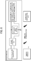
- FIG. 8 is a block diagram illustrating a sensor as an example of the electronic device of the present disclosure.
- a photoelectric converter, a power control IC, and a rechargeable device are combined to supply electricity to the power source of the control circuit of the sensor.
- This configuration can constitute a sensor module without connecting to a power source disposed outside or replacing batteries.
- the sensor can be applied to sense temperature and humidity, illuminance, human being, CO 2 , acceleration, ultravioret (UV), noise, geomagnetism, air pressure, and the like.
- a sensor module A senses a target at regular intervals and is configured to communicate the read data to a device such as a computer and a smartphone by wireless connection.
- the number of sensors is expected to be drastically increasing on the onset of society with the Internet. Replacing batteries one by one for such a great number of sensors takes time and effort and is not realistic. It is difficult to replace batteries of sensors disposed at places such as ceilings and walls. Supplying power with photoelectric converters is significantly advantageous.
- the photoelectric converter of the present disclosure can output high power at low illumination and the output does not significantly depend on the light entering angle; the freedom of positioning sensors is high.
- FIG. 9 is a block diagram illustrating a turntable as an example of the electronic device of the present disclosure.
- a photoelectric converter, a power control IC, and a rechargeable device are combined to supply electricity to the power source of the control circuit of the turntable.
- This configuration can constitute a turntable without connecting to a power source disposed outside or replacing batteries.
- turntables are placed in a show case displaying merchandise.
- Wiring of power sources looks bad and is not aesthetic.
- Merchandise should be removed when replacing batteries, which takes a lot of time and effort.
- the photoelectric converter of the present disclosure is effective to solve such problems.
- the photoelectric converter of the present disclosure and the photoelectric conversion module of the present disclosure are functional as stand alone power supplies; devices are operable with the electricity generated by photoelectric conversion thereof. It is not necessary to connect electronic devices with power sources or replace batteries for them because the photoelectric converter of the present disclosure and the photoelectric conversion module of the present disclosure can generate electricity upon irradiation of light. Electronic devices are operable and wearable even when a power source is unavailable. Electronic devices are operable without battery replacement when battery is not readily replaced. Dry cells make electronic devices heavy or bulky, which makes it difficult to install the electric devices on wall or ceiling or degrades their portability. On the other hand, the photoelectric converter of the present disclosure and the photoelectric conversion module of the present disclosure have a wide latitude of installation and are wearable and portable because they are thin and light-weighed.
- the photoelectric converter of the present disclosure and the photoelectric conversion module of the present disclosure can be used as stand alone power sources and can be combined with electronic devices.
- the photoelectric converter and the photoelectric conversion module can be combined with displays for devices such as desk calculators, wristwatches, mobile phones, electronic organizers, and electronic paper, peripherals to computers such as mice or keyboards, sensors such as temperature and humidity sensors and human sensitive sensors, transmitters such as beacons or global position system (GPS), auxiliary lights, and remote controllers.
- the photoelectric converter of the present disclosure and the photoelectric conversion module of the present disclosure can generate electricity at low illuminance.
- Low illuminance means 20 to 1,000 lux, which is common in interior environments with lighting. This illuminance is very weak in comparison with sunlight (approximately, 100,000 lux). These devices are widely applicable because they can generate electricity indoors or even in dim lit places (e.g., shadowed portions). Moreover, the photoelectric converter and the photoelectric conversion module are free of liquid leakage unlike dry cells and safe unlike button cells because they are not swallowed by mistake. These can be used as auxiliary power sources to make the continuous operation hours of rechargeable or dry-cell driven electric appliances longer.
- the photoelectric conversion of the photoelectric converter of the present disclosure and the photoelectric conversion module of the present disclosure are combined with a device that is operable on the electricity generated by photoelectric conversion of the photoelectric converter and the photoelectric conversion module, the device becomes highly usable, safe, and convenient, has a wide latitude of installation, and is effective to reduce the burden on the environment.
- FIG. 1 is a diagram illustrating a basic configuration of a device including one or both of the photoelectric converter of the present disclosure and the photoelectric conversion module of the present disclosure with an electronic device operable on the electricity generated by photoelectric conversion thereof.
- the photoelectric converter generates electricity at irradiation of light to take out electricity.
- the circuit of the device can operate on the electricity, yet the output of the electricity varies depending on the illuminance around the photoelectric converter so that the electronic device illustrated in FIG. 10 may not stably operate.
- a power control IC for the photoelectric converter can be effectively incorporated between the photoelectric converter and the circuit of the device to stably supply the voltage to the circuit.
- the photoelectric converter cannot generate target electricity. This is a drawback of the photoelectric converter.
- a rechargeable device such as a capacitor is disposed between the power control IC and the circuit of the device as illustrated in FIG. 12 . Owing to this configuration, the rechargeable device is charged with extra electricity from the photoelectric converter. The electricity stored in the rechargeable device is supplied to the circuit of the device when the photoelectric converter is not or insufficiently irradiated with light so that the electric device can be stably operated.
- an electronic device having a combination of one or both of the photoelectric converter of the present disclosure and the photoelectric conversion module of the present disclosure with the circuit of the electronic device is combined with a power control IC or a rechargeable device, the electronic device can operate in environment where a power source is unavailable and stably operates because it obviates the need for battery replacement.
- One or both of the photoelectric converter of the present disclosure and the photoelectric conversion module of the present disclosure can be used as a power source module. As illustrated in FIG. 13 , when one or both of the photoelectric converter of the present disclosure and the photoelectric conversion module of the present disclosure is connected with a power control IC for the photoelectric converter to constitute a direct current power source module, the power control IC can supply the electricity generated by photoelectric conversion of the photoelectric converter at a certain level of voltage.
- the rechargeable device when a rechargeable device is connected to the power control IC as illustrated in FIG. 14 , the rechargeable device is charged with the electricity generated by the photoelectric converter.
- They constitute a power source module capable of supplying power when the photoelectric converter is not or insufficiently irradiated with light.
- the power source module of the present disclosure illustrated in FIGS. 13 and 14 can be used without replacing batteries like a typical primary cell.
- PET polyethylene terephthalate
- ITO indium-doped tin oxide
- the surface roughness Ra of the ITO was measured with coherence scanning interferometer (VS1550, manufactured by Hitachi, Ltd.). Th resulting Ra was approximately 6 nm.
- a liquid of zinc oxide nano particles (average particle diameter of 12 nm (D), manufactured by Sigma-Aldrich Corporation) was spin-coated on an ITO filmed gas barrier PET film (15 ⁇ / ⁇ ) at 3,000 rotation per minute (rpm) followed by drying at 120 degrees C for 10 minutes to form an electron transport layer having an average thickness of 30 nm.
- the number of foreign objects having a diameter of 100 nm or greater present in a region of 100 ⁇ m ⁇ 100 ⁇ m of the surface of the electron transport layer was found to be approximately 10 or less with coherence scanning interferometer (VS1550, manufactured by Hitachi, Ltd.). No further treatment was made.
- a liquid application A of photoelectric conversion layer was prepared by dissolving 10 mg of poly(3-hexylthiophene) (P3HT) (number average molecular weight (Mn) of 54,000, manufactured by Sigma-Aldrich Corporation) and 10 mg of PC61BM (manufactured by Sigma-Aldrich Corporation) in 1 mL of chlorobenzene.
- P3HT poly(3-hexylthiophene)
- Mn number average molecular weight
- PC61BM manufactured by Sigma-Aldrich Corporation
- the liquid application A of photoelectric conversion layer was spin-coated on the electron transport layer at 1,000 rpm to form a photoelectric conversion layer having an average thickness of 200 nm (T).
- the difference between the average thickness and the minimum thickness of the photoelectric conversion layer in the effective power generation region was found to be approximately 60 nm.
- a hole transport layer of molybdenum oxide (manufactured by KOJUNDO CHEMICAL LABORATORY CO., LTD.) having a thickness of 20 nm and a second electrode made of gold having a thickness of 70 nm were sequentially vacuum-deposited on the photoelectric conversion layer.
- the photoreceptor of Example 1 was thus manufactured.
- a photoelectric converter was prepared in the same manner as in Example 1 except that the liquid application A of the photoelectric conversion layer was replaced with the following liquid application B of the photoelectric conversion layer.
- the difference between the average thickness and the minimum thickness of the photoelectric conversion layer in the effective power generation region was found to be approximately 60 nm.
- a photoelectric converter was prepared in the same manner as in Example 1 except that the liquid application A of the photoelectric conversion layer was replaced with a liquid application C of the photoelectric conversion layer followed by forming an electron transport layer and a photoelectric conversion layer in the following manner.
- a liquid of zinc oxide nano particle (average particle diameter of 12 nm (D), manufactured by Sigma-Aldrich Corporation) was spin-coated on an ITO filmed gas barrier PET film (15 ⁇ / ⁇ ) at 1,000 rpm followed by drying at 120 degrees C for 10 minutes to form an electron transport layer having an average thickness of 40 nm.
- the number of foreign objects having a diameter of 100 nm or greater present in a region of 100 ⁇ m ⁇ 100 ⁇ m of the surface of the electron transport layer was found to be approximately 10 or less with coherence scanning interferometer (VS1550, manufactured by Hitachi, Ltd.). No further treatment was made.
- the liquid application C of photoelectric conversion layer was prepared by dissolving 14 mg of the following compound 1 illustrated below (number average molecular weight (Mn) of 1,554) and 9 mg of the following compound 2 illustrated below in 1 mL of chloroform.
- the liquid application C of photoelectric conversion layer was spin-coated on the electron transport layer at 600 rpm to form a photoelectric conversion layer having an average thickness of 150 nm (T).
- the difference between the average thickness and the minimum thickness of the photoelectric conversion layer in the effective power generation region was found to be approximately 40 nm.
- a photoelectric converter was prepared in the same manner as in Example 3 except that an electron transport layer, a photoelectric transduction layer, a hole transport layer, a second electrode, and an insulating layer were formed in the following manner followed by sealing.
- a liquid of zinc oxide nano particles (average particle diameter of 12 nm (D), manufactured by Sigma-Aldrich Corporation) was spin-coated on an ITO filmed gas barrier PET film (15 ⁇ / ⁇ ) at 1,000 rpm followed by drying at 120 degrees C for 10 minutes to form an electron transport layer having an average thickness of 40 nm.
- An ethanol solution of dimethylamino benzoate was prepared at a content of 1 mg/mL on the electron transport layer to form a film on the zinc oxide nano particles at 1,500 rpm.
- the number of foreign objects having a diameter of 100 nm or greater present in a region of 100 ⁇ m ⁇ 100 ⁇ m of the surface of the electron transport layer was found to be approximately 10 or less with coherence scanning interferometer (VS1550, manufactured by Hitachi, Ltd.). No further treatment was made.
- the liquid application C of photoelectric conversion layer was spin-coated on the electron transport layer at 600 rpm to form a photoelectric conversion layer having an average thickness of 150 nm (T).
- the difference between the average thickness and the minimum thickness of the photoelectric conversion layer in the effective power generation region was found to be approximately 30 nm.
- a hole transport layer of molybdenum oxide (manufactured by KOJUNDO CHEMICAL LABORATORY CO., LTD.) having a thickness of 20 nm and a second electrode made of gold having a thickness of 70 nm were sequentially vacuum deposited on the photoelectric conversion layer.
- a liquid dispersion of aluminium oxide nano particles (manufactured by Sigma-Aldrich Corporation) was spin-coated on the prepared photoelectric converter at 1,500 rpm so that a 300 nm insulating layer was formed.
- a sealing member on which an adhesive layer was formed on PET covered with aluminium was applied to the insulating layer of the photoelectric converter to cover the photoelectric converter using a roll laminator.
- the PET substrate in the photoelectric converter and the sealing member were attached to each other followed by sealing.
- a photoelectric converter was prepared in the same manner as in Example 4 except that the liquid application C of the photoelectric conversion layer was replaced with the following liquid application D of the photoelectric conversion layer.
- the difference between the average thickness and the minimum thickness of the photoelectric conversion layer in the effective power generation region was found to be approximately 60 nm in Example 5.
- a photoelectric converter was prepared in the same manner as in Example 4 except that the liquid application C of the photoelectric conversion layer was replaced with the following liquid application E of the photoelectric conversion layer.
- the difference between the average thickness and the minimum thickness of the photoelectric conversion layer in the effective power generation region was found to be approximately 40 nm in Example 6.
- the liquid application E of photoelectric conversion layer was prepared by dissolving 15 mg of the compound 3 illustrated below (number average molecular weight (Mn) of 1,463) and 10 mg of the compound 2 illustrated above in 1 mL of chloroform.
- a photoelectric converter was prepared in the same manner as in Example 4 except that the average thickness of the photoelectric conversion layer was changed to 100 nm (T).
- the difference between the average thickness and the minimum thickness of the photoelectric conversion layer in the effective power generation region was found to be approximately 40 nm in Example 7.
- a photoelectric converter was prepared in the same manner as in Example 4 except that the liquid dispersion of zinc oxide nano particles for use in forming the electron transport layer was changed to a liquid dispersion of zinc oxide nano particles (average particle diameter of 30 nm (D), manufactured by TAYCA CORPORATION) to form a photoelectric conversion layer having an average thickness of 230 nm (T).
- D average particle diameter of 30 nm
- T photoelectric conversion layer having an average thickness of 230 nm
- the number of foreign objects having a diameter of 100 nm or greater present in a region of 100 ⁇ m ⁇ 100 ⁇ m of the surface of the electron transport layer was found to be approximately 10 or less in Example 8. No further treatment was made.
- the difference between the average thickness and the minimum thickness of the photoelectric conversion layer in the effective power generation region was found to be approximately 30 nm.
- a photoelectric converter was prepared in the same manner as in Example 4 except that the average thickness (T) of the photoelectric conversion layer was changed to 310 nm.
- the difference between the average thickness and the minimum thickness of the photoelectric conversion layer in the effective power generation region was found to be approximately 60 nm in Example 9.
- a photoelectric converter was prepared in the same manner as in Example 4 except that the liquid application C of the photoelectric conversion layer was replaced with the following liquid application F of the photoelectric conversion layer.
- the difference between the average thickness and the minimum thickness of the photoelectric conversion layer in the effective power generation region was found to be approximately 40 nm in Example 10.
- the liquid application F of photoelectric conversion layer was prepared by dissolving 12.5 mg of the compound 4 illustrated below (number average molecular weight (Mn) of 2,029) and 12.5 mg of the compound 2 illustrated above in 1 mL of chloroform.
- a photoelectric converter was prepared in the same manner as in Example 4 except that the substrate with first electrode was replaced with the following substrate with first electrode.
- a glass substrate (10 ⁇ / ⁇ ) on which ITO was formed was procured from Nippon Electric Glass Co., Ltd.
- the ITO was found to have a surface toughness Ra of approximately 5 nm.
- a photoelectric converter was prepared in the same manner as in Example 4 except that the electron transport layer was changed to the following and the average thickness of the photoelectric conversion layer was changed to 90 nm (T).
- the difference between the average thickness and the minimum thickness of the photoelectric conversion layer in the effective power generation region was found to be approximately 20 nm in Example 12.
- Aluminum-doped zinc oxide nano particle (average particle diameter of 12 nm (D), manufactured by Sigma-Aldrich Corporation) was spin-coated on an ITO filmed gas barrier PET film (15 ⁇ / ⁇ ) at 1,000 rpm followed by drying at 120 degrees C for 10 minutes to form an electron transport layer having an average thickness of 40 nm.
- the number of foreign objects having a diameter of 100 nm or greater present in a region of 100 ⁇ m ⁇ 100 ⁇ m of the surface of the electron transport layer was found to be approximately 10 or less. No further treatment was made.
- a photoelectric converter was prepared in the same manner as in Example 4 except that the electron transport layer was changed to the following and the average thickness of the photoelectric conversion layer was changed to 70 nm (T).
- the difference between the average thickness and the minimum thickness of the photoelectric conversion layer in the effective power generation region was found to be approximately 20 nm in Example 13.
- Tin oxide nano particles (average particle diameter of 7 nm (D), manufactured by Sigma-Aldrich Corporation) were spin-coated on an ITO filmed gas barrier PET film (15 ⁇ / ⁇ ) at 1,000 rpm followed by drying at 80 degrees C for 10 minutes to form an electron transport layer having an average thickness of 20 nm.
- the number of foreign objects having a diameter of 100 nm or greater present in a region of 100 ⁇ m ⁇ 100 ⁇ m of the surface of the electron transport layer was found to be approximately 10 or less. No further treatment was made.
- a photoelectric converter was prepared in the same manner as in Example 11 except that the electron transport layer was changed to the following.
- An ethanol liquid dispersion of zinc titanium nano particle paste (average particle diameter of 20 nm, manufactured by JGC Catalysts and Chemicals Ltd.) was spin-coated on an ITO filmed glass substrate (10 ⁇ / ⁇ , manufactured by Nippon Electric Glass Co., Ltd.) at 1,000 rpm followed by heating at 450 degrees C for 30 minutes to form an electron transport layer having an average thickness of 100 nm.
- the number of foreign objects having a diameter of 100 nm or greater present in a region of 100 ⁇ m ⁇ 100 ⁇ m of the surface of the electron transport layer was found to be approximately 10 or less. No further treatment was made.
- the difference between the average thickness and the minimum thickness of the photoelectric conversion layer in the effective power generation region was found to be approximately 30 nm in Example 14.
- a photoelectric converter was prepared in the same manner as in Example 4 except that the hole transport layer was changed to the following.
- Tungsten oxide manufactured by KOJUNDO CHEMICAL LABORATORY CO., LTD. was deposited onto the photoelectric conversion layer to form a hole transport layer having an average thickness of 20 nm.
- a photoelectric converter was prepared in the same manner as in Example 4 except that the hole transport layer was changed to the following.
- Vanadium oxide (manufactured by KOJUNDO CHEMICAL LABORATORY CO., LTD.) was deposited onto the photoelectric conversion layer to form a hole transport layer having an average thickness of 20 nm.
- a photoelectric converter was prepared in the same manner as in Example 4 except that the average thickness of the photoelectric conversion layer was changed to 470 nm (T).
- the difference between the average thickness and the minimum thickness of the photoelectric conversion layer in the effective power generation region was found to be approximately 50 nm in Example 17.
- a photoelectric converter was prepared in the same manner as in Example 4 except that the average thickness of the photoelectric conversion layer was changed to 550 nm (T).
- the difference between the average thickness and the minimum thickness of the photoelectric conversion layer in the effective power generation region was found to be approximately 50 nm in Example 18.
- a photoelectric converter was prepared in the same manner as in Example 4 except that the liquid dispersion of zinc oxide nano particles for use in forming the electron transport layer was changed to a liquid dispersion of zinc oxide nano particles (average particle diameter of 30 nm (D), manufactured by TAYCA CORPORATION).
- the number of foreign objects having a diameter of 100 nm or greater present in a region of 100 ⁇ m ⁇ 100 ⁇ m of the surface of the electron transport layer was found to be approximately 10 or less in Comparative Example 1. No further treatment was made.
- a photoelectric converter was prepared in the same manner as in Example 4 except that the average thickness of the photoelectric conversion layer was changed to 70 nm (T).
- the difference between the average thickness and the minimum thickness of the photoelectric conversion layer in the effective power generation region was found to be approximately 20 nm in Comparative Example 2.
- a photoelectric converter (Organic solar cell Module #3) was procured from InifinityPV ApS as the photoelectric converter of Comparative Example 3.
- the details of the material and the layer structure of the photoelectric converter of Comparative Example 3 are unavailable.
- the photoelectric converter of Comparative Example 3 had an extremely high density of current leakage. The density could not be precisely measured; it is, however, inferred that the ratio of current leakage was 0.99 or greater at an illuminance of 200 lux.
- the highest occupied molecular orbital (HOMO) of the photoelectric conversion layer of the obtained photoelectric converter was measured using a photoemission yield spectroscopy in air (AC-2, manufactured by RIKEN KEIKI Co., Ltd.).
- the current-voltage of each of the obtained photoelectric converters were measured at an illuminance of white light emitting diode (LED) illumination of 100, 200, 2,000, 5,000, 10,000, and 18,000 lux.
- LED white light emitting diode
- the white LED was a light-bulb form LED lamp (LDA11N G/100 W, manufactured by TOSHIBA Lighting & Technology Corporation).
- the current-voltage was measured using an evaluation device (source meter, KEYSIGHT B2902A).
- the illuminance of the white LED illumination was measured with an illuminometer (510 LUX METER, manufactured by Yokogawa Electric Corporation).
- the ratio P L of current leakage was obtained by the device evaluation and the current leakage ratio P L mentioned above using the density of short circuit current obtained at each illuminance and the values of open-circuit voltage.
- ⁇ 100 and ⁇ 20000 respectively represent energy conversion efficiency at an illuminance of 100 lux and 20,000 lux of the light source.
- the ratio of the average particle diameter of the metal oxide particles and the average thickness of the photoelectric conversion layer were obtained for each photoelectric converter.
- the average particle diameter (D) of the metal oxide particle was measured as described above.
- the average thickness of the photoelectric conversion layer was measured according to the method described above.
- Example 1 HOMO level of photoelectric conversion layer Ratio P ⁇ of energy conversion efficiency Ratio P L of current leakage Average particle diameter (D) of metal oxide particle Average thickness (T) (nm) of photoelectric conversion layer Ratio (T/D)
- Example 1 4.9 eV 0.81 0.66 12 200 16.7
- Example 2 5.1 eV 0.82 0.65 12 200 16.7
- Example 3 5.2 eV 0.80 0.68 12 150 12.5
- Example 4 5.2 eV 0.86 0.62 12 150 12.5
- Example 5 5.2 eV 0.76 0.71 12 150 12.5
- Example 6 5.3 eV 0.80 0.67 12 150 12.5
- Example 7 5.2 eV 0.75 0.81 12 100 8.3
- Example 8 5.2 eV 0.74 0.83 30 230 7.6
- Example 9 5.2 eV 0.91 0.59 12 310 25.8
- Example 10 5.3 eV 0.80 0.68 12 150 12.5
- Example 11 5.2 eV 0.86 0.64 12 150 12.5
- every photoelectric converter of Examples 1 to 18 had a ratio P L of current leakage of 0.95 eV or less.
- the ratio of the energy conversion efficiency at a low illumination environment against the energy conversion efficiency in a high illumination environment was 70 percent or more; the photoelectric conversion efficiency at a low illumination environment does not significantly deteriorate in comparison with the photoelectric conversion efficiency in a high illumination environment.
- the ratio P L of current leakage of the photoelectric converters of Comparative Examples 1 to 3 surpasses 0.95; the energy conversion efficiency in a low illumination environment is down more than 50 percent in comparison with the photoelectric conversion efficiency in a high illumination environment.
Landscapes
- Physics & Mathematics (AREA)
- Electromagnetism (AREA)
- Chemical & Material Sciences (AREA)
- Inorganic Chemistry (AREA)
- Photovoltaic Devices (AREA)
- Electroluminescent Light Sources (AREA)
- Charge And Discharge Circuits For Batteries Or The Like (AREA)
Abstract
Description
- The present disclosure relates to a photoelectric converter, a photoelectric conversion module, an electronic device, and a power source module.
- Internet of Things (IOT) is expected to be a way of comprehensively controlling the society system by connecting all things to the Internet. Before such an IOT society is realized, many sensors need to be connected to all kinds of things to acquire data and power supplies to operate sensors; it is, however, not practical to wire many sensors and use many rechargeable batteries. Energy harvesting elements for power source are expected to reduce the burden on the environment, which is a great concern of society.
- Of such elements, photoelectric converters are appealing because they can generate electricity anywhere upon application of light. Flexible photoelectric converters, in particular, are required to be highly efficient. They are expected to be traceable to curved surfaces and applicable to wearable devices. Feasibility on these applications was discussed and reported in Applied Physics letters 108,253301 (published in 2016) and Japanese Journal of Applied Physics 54,071602 (published in 2015).
- Organic thin film solar cells are expected to be highly efficient and flexible energy harvesting elements. One example of such elements is a photoelectric converter having a transparent substrate film as a substrate, which has been proposed in
JP-2014-220333-A1 - A housing for mobile electronic device has been proposed in
JP-2016-208568-A1 - According to the present disclosure, a photoelectric converter is provided which achieves excellent photoelectric conversion even in low illumination environment in comparison with a high illumination environment.
- According to embodiments of the present disclosure, a photoelectric converter (1) is provided which includes a substrate (2), a first electrode (3) on the substrate (2), an electron transport layer (4) overlying the first electrode (3), a photoelectric conversion layer (5) overlying the electron transport layer (4), the photoelectric conversion layer (5) containing at least two types of organic materials, a hole transport layer (6) overlying the photoelectric conversion layer (5), and a second electrode (7) overlying the hole transport layer (6), wherein the photoelectric converter (1) has a ratio PL of current leakage of 0.95 or less at an illuminance of 200 lux, where the ratio PL is calculated from the following equation (1): PL = L/Jph Equation (1), where L represents a density (µA/cm2) of current leakage at an illuminance of 200 lux and Jph represents a density (µA/cm2) of photocurrent density at an illuminance of 200 lux.
- Various other objects, features and attendant advantages of the present invention will be more fully appreciated as the same becomes better understood from the detailed description when considered in connection with the accompanying drawings in which like reference characters designate like corresponding parts throughout and wherein:
-
FIG. 1 is a diagram illustrating an organic thin film solar cell as an example of the photoelectric converter according to an embodiment of the present disclosure; -
FIG. 2 is a graph plotting the open-circuit voltage Voc (V) per cell to In (Jph); -
FIG. 3 is a block diagram illustrating a mouse for computer as an example of the electronic device according to an embodiment of the present disclosure; -
FIG. 4 is a schematic diagram illustrating an example of the mouse illustrated inFIG. 3 ; -
FIG. 5 is a block chart illustrating a keyboard for computer as an example of the electronic device according to an embodiment of the present disclosure; -
FIG. 6 is a schematic diagram illustrating an example of the keyboard illustrated inFIG. 5 , -
FIG. 7 is a schematic diagram illustrating another example of the keyboard illustrated inFIG. 5 ; -
FIG. 8 is a block diagram illustrating a sensor as an example of the electronic device according to an embodiment of the present disclosure; -
FIG. 9 is a block diagram illustrating a turntable as an example of the electronic device according to an embodiment of the present disclosure; -
FIG. 10 is a block diagram illustrating an example of the electronic device according to an embodiment of the present disclosure; -
FIG. 11 is a block diagram illustrating an example in which a power control IC is incorporated into the electronic device illustrated inFIG. 10 ; -
FIG. 12 is a block diagram illustrating an example in which a rechargeable device is further incorporated into the electronic device illustrated inFIG. 11 ; -
FIG. 13 is a block diagram illustrating an example of the power source module according to an embodiment of the present disclosure; and -
FIG. 14 is a block diagram illustrating an example in which a rechargeable device is incorporated into the power source module illustrated inFIG. 13 . - The accompanying drawings are intended to depict example embodiments of the present invention and should not be interpreted to limit the scope thereof. The accompanying drawings are not to be considered as drawn to scale unless explicitly noted. Also, identical or similar reference numerals designate identical or similar components throughout the several views.
- In describing embodiments illustrated in the drawings, specific terminology is employed for the sake of clarity. However, the disclosure of this specification is not intended to be limited to the specific terminology so selected and it is to be understood that each specific element includes all technical equivalents that have a similar function, operate in a similar manner, and achieve a similar result.
- As used herein, the singular forms "a", "an", and "the" are intended to include the plural forms as well, unless the context clearly indicates otherwise.
- Moreover, image forming, recording, printing, modeling, etc., in the present disclosure represent the same meaning, unless otherwise specified.
- Embodiments of the present invention are described in detail below with reference to accompanying drawing(s). In describing embodiments illustrated in the drawing(s), specific terminology is employed for the sake of clarity. However, the disclosure of this patent specification is not intended to be limited to the specific terminology so selected, and it is to be understood that each specific element includes all technical equivalents that have a similar function, operate in a similar manner, and achieve a similar result.
- For the sake of simplicity, the same reference number will be given to identical constituent elements such as parts and materials having the same functions and redundant descriptions thereof omitted unless otherwise stated.
- Within the context of the present disclosure, if a first layer is stated to be "overlaid" on, or "overlying" a second layer, the first layer may be in direct contact with a portion or all of the second layer, or there may be one or more intervening layers between the first and second layer, with the second layer being closer to the substrate than the first layer.
- The photoelectric converter includes a substrate, a first electrode on the substrate, an electron transport layer overlying the first electrode, a photoelectric conversion layer overlying the first electrode, the photoelectric conversion layer containing at least two types of organic materials, a hole transport layer overlying the photoelectric conversion layer, and a second electrode overlying the hole transport layer, wherein the photoelectric converter has a ratio PL of current leakage of 0.95 or less at an illuminance of 200 lux, where the ratio PL is calculated from the following equation (1):

- In the equation (1), L represents a density (µA/cm2) of current leakage at an illuminance of 200 lux and Jph represents a density (µA/cm2) of photocurrent at an illuminance of 200 lux.
- In the specification of the present disclosure, "photoelectric converter" means an element that converts light energy into electric energy or the other way round and includes a solar cell and a photodiode.
- An organic thin film solar cells as an example of the photoelectric converter can be readily made flexible in comparison with an inorganic solar cell, which uses an inorganic crystalline material such as crystal silicon; it is, however, necessary to make the photoelectric conversion layer in an organic thin film solar cell thinner to achieve sufficient attributes because the photoelectric conversion layer is composed of an organic material having a smaller diffusion length of a carrier than an inorganic crystalline material. The average thickness of a photoelectric conversion layer made of organic materials is in general around several hundred nanometers. This average thickness is extremely thinner than that of a crystalline silicon solar cell, which is an order of micro meter; it is necessary to secure a uniform thickness of such a thin photoelectric conversion layer when it is formed by a solution process in particular. The solution process is used in general to form layers including the photoelectric conversion layer because the process is cost effective. However, if a non-uniform photoelectric conversion layer is formed owing to the malformation of film or the presence of impurities, the electron transport layer and the hole transport layer contact each other and moreover, the first electrode and the second electrode directly contact each other; the current is leaked from portions having a low resistance. Such current leakage damages the attributes of the photoelectric conversion of the organic thin film solar cell. What impact this leakage has on the attributes of photoelectric conversion is known to be dependent on the amount of light entering into an organic thin film solar cell; the attributes of photoelectric conversion deteriorate as the amount of light decreases.
- In fact, even an organic thin film solar cell having a certain level of photoelectric conversion attributes in an environment of a relatively large amount of light such as reference sunlight reduces the output power more than the decreases in the input energy in an environment of a small amount of light such as indoor environment. The attributes of a photoelectric converter including an organic thin film solar cell can be evaluated by the following three parameters: Jsc, the density (A/cm2) of short circuit current in which the photoelectric converter is short-circuited; Voc (V) of open-circuit voltage of a photoelectric converter at an open state; and FF, the curve factor of voltage-current curve. The energy conversion efficiency η against the incident light energy Pin (W/cm2) is represented by the following equation (2).

-
JP-2016-208568-A1 - As described above, an organic thin film solar cell as an example of the photoelectric converter is required to be thin in principle. Such a thin film causes a drawback such as current leakage. This current leakage causes a problem of a drop of the output power in particular in an low illumination environment such as indoor light. The present inventors have formulated a solution to the problem, which is controlling the relative ratio (ratio of current leakage) of the density of current leakage to the density of photocurrent.
- An environment of illumination light including visible light is assumed for the photoelectric converter of the present disclosure. Since illuminance (lux) is used to indicate the amount of light in general, illuminance is regulated in the present disclosure. As the reference illuminance, the reference of minimum illuminance in each environment is regulated in JIS Z 9110:2010 format. Normal visual operation in an ordinary manufacturing factory requires at least 500 lux and other types of operations at a warehouse require at least 200 lux. On the other hand, 1 SUN as the reference sunlight is about 100,000 lux and known to be by several hundreds to several thousands larger than the illuminance in an indoor environment.
- Having investigated photoelectric converters having a high energy conversion efficiency in an environment of a small light amount such as in indoor light environment without significantly deteriorating from that in an environment of a relatively large light amount, the present inventors have focused on the current leakage mentioned above.
- As a result of the investigation on the current leakage, the present inventors have acquired the knowledge that the photoelectric conversion of a photoelectric converter deteriorate in an environment of low illumination such as indoor environment when the relative ratio of the density of the current leakage to the density of photocurrent surpasses a certain level. The present inventors have found that the density of the current leakage is necessary to decrease to obtain a photoelectric converter having a high photoelectric conversion in an environment of low illumination. The present disclosure was thus made.
- The photoelectric converter of the present disclosure includes at least a substrate, a first electrode on the substrate, an electron transport layer, a photoelectric conversion layer, a photoelectric conversion layer containing at least two types of organic materials, a hole transport layer, a second electrode, wherein the photoelectric converter has a ratio PL of current leakage of 0.95 or less at an illuminance of 200 lux, where the ratio PL is calculated from the following equation (1):

- In the equation (1), L represents a density (µA/cm2) of current leakage at an illuminance of 200 lux and Jph represents a density (µA/cm2) of photocurrent density at an illuminance of 200 lux.
- The device evaluation and the current leakage ratio PL are obtained in the following manner.
- The current-voltage attribute is measured changing the illuminance of light to which a device is exposed with a source meter capable of measuring the density of short circuit current and the open-circuit voltage of a target photoelectric converter in an arbitrary illumination. It is preferable to use the same light source regardless of illuminance, yet it is possible to use another illumination when using the same light source is difficult as long as the difference in the color temperatures between the two illuminations is within an absolute value of 200 K.
- The ratio PL of current leakage at an illuminance of 200 lux can be calculated from the following equation (1):

- In the equation (1), L represents a density (µA/cm2) of current leakage at an illuminance of 200 lux and Jph represents a density (µA/cm2) of photocurrent at an illuminance of 200 lux.
- The density L (µA/cm2) of current leakage at an illuminace of 200 lux can be obtained by assigning the values of the density Jsc (µA/cm2) of short circuit current and the open-circuit voltage Voc (V) per cell obtained at the measurements at an illuminance of 200 lux into the following equation (3).

- In the equation (3), Jph represents the density (µA/cm2) of photocurrent. Hereinafter, it is treated as equal to Jsc for convenience. Jo represents the density (µA/cm2) of dark current, q represents elementary charge (= 1.602 × 10⁻¹⁹ C), n represents ideality factor, k represents Boltzmann's constant (= 1.38 × 10⁻²³ cm2•kg•s-2•K-1), and T represents the temperature (K) of a device.
- In the case of a photoelectric conversion module in which multiple cells are connected in series, the value obtained by dividing the open-circuit voltage Voc_mod of the entire module by the number of series Nmod is defined as Voc as shown in the following equation (4).

- Jo and n in the equation (3) are values calculated from VOC - 1n(Jph) plotting obtained by measurements at three or more points arbitrarily-selected from 2,000 to 20,000 lux realized at the illumination mentioned above.
FIG. 2 is a graph illustrating an example of plotting Voc - 1n(Jph). - The plots can be approximate to a straight line when the density of current leakage mentioned above is sufficiently small. When the decline of the regression line obtained by the least squares method is defined as m and the intercept against the 1n(Jph) axis is defined as 1n(JO) regarding the points corresponding to the measurements at the three or more points, n can be obtained from the following equation (5) and JO can be obtained from the axis intercept. The coefficient of determination of the regression line is preferably 0.99 or greater.

- n normally ranges from 1 to 2. When n surpasses 2 or JO calculated by the method described above surpasses 0.01 (µA/cm2), the ratio PL of current leakage cannot be correctly calculated by the method mentioned above because the current leakage is extremely large. The current leakage ratio in this case is at least above 0.95. Conversely, when the density of current leakage is extremely small, the density of current leakage may be negative owing to the measuring error. In such a case, the density of current leakage is regarded as 0 (µA/cm2).
- The way or condition of preparing the photoelectric converter satisfying the requisite of the ratio PL of current leakage of 0.95 or less is not particularly limited and can be suitably selected to suit to a particular application. It includes, for example, the following (1) to (4).
- (1) A photoelectric converter includes a substrate, a first electrode on the substrate, an electron transport layer on the first electrode, a photoelectric conversion layer on the first electrode, the photoelectric conversion layer containing at least two types of organic materials, a hole transport layer on the photoelectric conversion layer, a second electrode on the hole transport layer, and an insulating layer on the second electrode, wherein the first electrode contains a transparent electroconductive film, wherein the following relationship is satisfied: 7.0 ≦ T/D, where T represents the average thickness of the photoelectric conversion layer and D represents the average particle diameter of the metal oxide particles.
- (2) The surface of the first electrode is preferably smooth. The surface roughness Ra is preferably less than 10 nm. The surface is preferably free of impurities. If the surface of the first electrode is not sufficiently smooth or impurities are present on the surface of the first electrode, the surface of film formed on the first electrode becomes rough. Such a rough surface may increase the density of the current leakage.
Impurities can be removed by: dipping a substrate on which the first electrode is formed in a liquid such as a rinsing liquid, an organic solvent, and pure water followed by rinsing with ultrasonic wave; or subjecting the surface of the first electrode to air pressure plasma treatment or UV-O3 treatment. - (3) It is preferable that the average thickness of the electron transport layer be approximately 20 nm or greater and impurities be little or never present on the surface. The agglomerated matter of the material of the electron transport layer is regarded as one of the impurities. It is preferable that the number of impurities having a diameter of 100 nm or greater on the surface of an electron transport layer be 10 or less in a region of 100 µm × 100 µm of the surface; impurities present on the surface of an electron transport layer may cause the surface of the photoelectric conversion layer rough and increase the density of current leakage.
Such impurities can be removed by air pressure plasma treatment to the surface of an electron transport layer or selectively burn off the impurities with laser beams in accordance with their absorption wavelengths. - (4) It is preferable that the average thickness of the photoelectric conversion layer be approximately 100 nm or greater and the variance of the thickness be minimal. It is preferable that the minimum thickness of the photoelectric conversion layer in the effective power generation region be at least 75 percent of the average thickness. If the thickness of the photoelectric conversion layer varies portion by portion, the density of the current leakage may increase owing to the mechanism described above. To reduce the variance of the thickness, the following can be optimized: the concentration of liquid application; the solvent for the liquid application; and the application method.
- It is possible to achieve a ratio PL of current leakage of 0.95 or less by all of (2) to (4) mentioned above; an average thickness of the hole transport layer of 50 nm or greater can further reduce the density of current leakage.
- The substrate is transparent and flexible film or glass which is not flexible but flat.
- Specific examples of the film include, but are not limited to, polyester such as polyethylene terephthalate, polycarbonate, polyimide, polymethyhlmethacrylate, polysulfone, and polyetheretherketone. The substrate includes a thin film glass having an average thickness of 200 µm or less. Of these films, polyester, polyimide, and thin-film glass are preferable because they are readily and cost-effectively manufactured.
- If a plastic substrate is used, it is preferable to provide it with a gas barrier layer.
- A gas barrier is a layer for preventing transmission of vapor oxygen. A gas barrier having such a function is not particularly limited and can be suitably selected to suit to a particular application. A specific example is a plastic substrate covered with aluminum.
- The first electrode is mainly composed of a transparent electroconductive film. The first electrode may have a structure of a transparent electroconductive film, a thin metal film layer, and a transparent electroconductive film laminated in this order.
- The same or different materials can be used for the transparent electroconductive films sandwiching the thin metal film.
- Specific examples of the material for use in the transparent electroconductive film include, but are not limited to, tin-doped indium oxide (ITO), zinc-doped indium oxide (IZO), zinc oxide (ZnO), aluminium-doped zinc oxide (AZO), gallium-doped zinc oxide (GZO), and tin oxide (SnO2). Of these, ITO, IZO, and AZO are preferable.
- The average thickness of the transparent electroconductive film is preferably 30 nm or greater and more preferably from 40 to 150 nm.
- The transparent electrode preferably has a sheet resistance of 50 Ω/□ or less, more preferably 30 Ω/□ or less, and furthermore preferably 20 Ω/□ or less.
- The transparent electrode preferably has a high level of transparency. Its transparency is preferably 60 percent or higher and more preferably 70 percent or higher. The upper limit is not particularly limited and can be suitably selected to suit to a particular application; 90 percent or less is preferable.
- The electron transport layer is formed on or overlying the first electrode.
- The electron transport layer preferably contains metal oxide particles. The layer can be formed by applying a liquid dispersion of the metal oxide particles followed by drying. The metal oxide particles preferably have an n-type semiconductor property. Particles of zinc oxide, titanium oxide, and tin oxide are preferable. The metal oxide particle may be doped with other metals.
- Specific examples of the metal oxide for use in the electron transport layer include, but are not limited to, zinc oxide, aluminium-doped zinc oxide, gallium-doped zinc oxide, titanium oxide, and tin oxide.
- The average particle diameter (D) of the nano-particulate metal oxide particles is preferably from 1 to 50 nm and more preferably from 5 to 20 nm.
- The average thickness of the electron transport layer is preferably from 10 to 60 nm and more preferably from 15 to 40 nm.
- The average particle diameter (D) of the metal oxide particles can be measured in the following manner.
- A solution of the metal oxide particle is moved to a glass nebulizer with a micro pipette. The solution is sprayed from the nebulizer to a grid with collodion film for transmission electron microscopy (TEM). The grid is deposited with carbon using physical vapor deposition (PVD) method to acquire images of metal oxide particles with an electron microscope. The obtained image is subjected to image processing to measure the particle diameter of the metal oxide particles.
- The cross sectional surface of the photoelectric converter is observed with a scanning TEM. Particles are recognized with image processing followed by measuring the particle diameter of the metal oxide particles. The particle size distribution can be measured by laser diffraction/scattering. The method of cross-sectional surface exposure, observation with TEM, and measuring of particle size distribution are already well-known.
- In the present disclosure, the particle diameter of each of at least randomly selected hundred metal oxide particles is measured and averaged to obtain the average particle diameter of the metal oxide particles.
- The electron transport layer preferably has a structure of a first electron transport layer containing the metal oxide particles and a second electron transport layer between the first electron transport layer and the photoelectric conversion layer.
- The second electron transport layer preferably contains an amine compound represented by the following Chemical Formula (4).

- In the Chemical Formula (4), R4 and R5 each, independently substituted or non-substituted alkyl groups having 1 to 4 carbon atoms.
- X represents a divalent aromatic group having 6 to 14 carbon atoms or an alkyl group having 1 to 4 carbon atoms,
R4 and R5 can share a linkage to form a ring. A represents one of -COOH, -P(=O)(OH2), and -Si(OH)3. - The photoelectric conversion layer is formed on or overlying the electron transport layer.
- The photoelectric conversion layer contains two or more types of organic materials and may contain furthermore optionally other components.
- One of the organic materials of the two or more types of organic materials contained in the photoelectric conversion layer is an electron donor and the others are electron acceptors. The electron donor is also referred to as a p-type organic semiconductor material and the electron acceptor is referred to as an n-type organic material.
- The photoelectric conversion layer preferably has a bulk hetero structure containing a mixture of these materials.
- The type of the electron donor used is not particularly limited and can be suitably selected to suit to a particular application. The electron donor is preferably a π-electron conjugated compound having a highest occupied molecular orbital (HOMO) level of from 5.1 to 5.5 eV.
- Specific examples include, but are not limited to, conjugated polymers obtained by coupling aromatic series derivatives such as thiophen, fluorene, carbazole, thienothiophene, benzodithiophene dithienosilole, quinoxaline, and benzothiadiazole, and porphyrin and phthalocyanine, which are conjugated compounds having clearly identified low molecular weights. They also include organic materials such as donor-acceptor linking materials having an electron donating portion and an electron accepting portion in the molecule.
- Of these electron donors, the materials for electron donor (P-type semiconductor) made of low molecular weight conjugated compounds having a number average molecular weight of 10,000 or less are more preferable. The number average molecular weight is more preferably 5,000 or less.
- Specific examples of the one of the organic materials of the two or more types of organic materials contained in the photoelectric conversion layer include, but are not limited to, compounds represented by the following Chemical Formula (1).
- Specific examples of the electron donor having a highest occupied molecular orbital (HOMO) level of from 5.1 to 5.5 eV and a number average molecular weight of 10,000 or less include, but are not limited to, the compounds represented by the following Chemical Formula (1).

- In the Chemical Formula (1), R1 represents an alkyl group having 2 to 8 carbon atoms. n represents an integer of from 1 to 2. X represents one of the following Chemical Formula (2) and the following Chemical Formula (3).


- In the Chemical Formulae (2) and (3), R2 and R3 each, independently represent linear or branched alkyl groups. The linear or branched alkyl group preferably has 2 to 30 carbon atoms.
- Specific examples of the compound represented by the Chemical Formula (1) are illustrated below but are not limited thereto.


- The type of electron acceptor organic material as the other organic material mentioned above is not particularly limited and can be suitably selected to suit to a particular application. It is preferably a π electron conjugated compound having a lowest occupied molecular orbital (LOMO) level of from 3.5 to 4.5 eV.
- Example of the other organic material are electron acceptors (N-type semiconductor) below. Specific examples include, but are not limited to, fullerene or its derivatives, naphthalene tetracarboxylic acid imide derivatives, and perylene teracarboxylic acid imide derivatives. Of these, fullerene derivatives are more preferable.
- Specific examples of the fullerene derivatives include, but are not limited to, C60, phenyl-C61-methyl lactate (fullerene derivatives referred to as PCBM, [60]PCBM, or PC61BM in documents), C70, phenyl-C-71-methyl lactate (fullerene derivatives referred to as PCBM, [70]PCBM, or PC71BM in documents), and fullerene derivatives mentioned in the web site of DAIKIN INDUSTRIES, LTD.
- The average thickness of the photoelectric conversion layer is preferably from 50 to 400 nm and more preferably from 60 to 250 nm. An average thickness of 50 nm or greater effectively prevents a problem of insufficient production of carriers owing to deficiency of light absorption by the photoelectric conversion layer. An average thickness of 400 nm or less effectively prevents the degradation of transport efficiency of carriers produced by light absorption
- The present inventors have found that the relationship between the thicknesses of the electron transport layer and the photoelectric conversion layer have an great impact on reducing the ratio of current leakage.
- When the average particle diameter of the metal oxide particles in the electron transport layer is defined as D and the average thickness of the photoelectric conversion layer is defined as T, the following relationship is satisfied: 7.0 ≦ T/D.
- When T/D is less than 7.0, the probability of the contact between the metal oxide particles and the hole transport layer increases, thereby increasing the density of current leakage; it is, however, possible to reduce the density of current leakage by increasing the average thickness of the photoelectric conversion layer by 7 times or more as large as the average particle diameter of the metal oxide particles. A ratio T/D of 10 or more significantly decreases the probability of the contact between the metal oxide particles and the hole transport layer and furthermore decreases the density of current leakage.
- The average thickness T of the photoelectric conversion layer can be measured in the following manner.
- A photoelectric conversion layer is applied onto a substrate and thereafter arbitrarily selected nine sites of the film are wiped with a solvent. The steps at the nine wiped sites are measured with DEKTAK manufactured by Bruker Corporation. The average of the measurements is defined as the average thickness T of the photoelectric conversion layer.
- The cross sectional surface is observed with scanning electron microscope (SEM) or TEM to obtain the average thickness of the photoelectric conversion layer.
- In the present disclosure, it is possible to sequentially apply the organic material to form a planar junction interface; it is, however, preferable to form a bulk heterojunction formed by three-dimensionally mixing the organic materials to increase the junction interface area.
- A material highly soluble in a solvent is dissolved in a solvent to prepare a liquid mixture of each organic material in a form of molecule. After the liquid mixture is applied, the resulting material is dried followed by removing the solvent to form a bulk heterojunction. Optionally, this junction may be heated to optimize the agglomeration state of each semiconductor.
- When a material poorly soluble in a solvent is used, a liquid dispersion is prepared in which the organic material is dissolved in a solvent and then the liquid dispersion is applied to form a mixture layer. Optionally, this mixture layer may be heated to optimize the agglomeration state of each semiconductor.
- Thin film of the organic material can be formed by methods such as spin coating, blade coating, slid die coating, screen printing, bar coater application, mold application, print transfer method, dip drawing-up method, inkjet method, spraying method, and vacuum deposition method. Of these, a suitable method can be selected to control the thickness and arrangement to suit to attributes of thin film of organic material to be prepared.
- In the case of a spin coating, it is preferable to use a solution containing a P-type semiconductor material having a structure represented by the Chemical Formula (1) illustrated above and an N-type material semiconductor material in a range of a content of from 5 to 40 mg/mL.
- The content here means the mass of the P-type semiconductor material having a structure represented by the Chemical Formula (1) illustrated above and the N-type semiconductor material to the volume of a solution containing the P-type semiconductor material having a structure represented by the Chemical Formula (1) illustrated above, the N-type semiconductor material, and the solvent. Such a content makes it easy to prepare a uniform photoelectric conversion layer.
- Prepared photoelectric conversion layers may be subjected to annealing with a reduced pressure or in an inert gas atmosphere (nitrogen, argon atmosphere) to remove the solvent. The temperature during annealing is preferably from 40 to 300 degrees C and more preferably from 50 to 150 degrees C. The contact area at which laminated layers permeate each other at the interface increases by annealing, which may increase a short-cut current. The annealing may be conducted after forming an electrode.
- The solvent to be mixed with the P-type semiconductor material having a structure represented by the Chemical Formula (1) illustrated above and the N-type semiconductor material is not particularly limited and can be suitably selected to suit to a particular application.
- Specific examples include, but are not limited to, methanol, ethanol, butanol, toluene, xylene, o-chlorophenol, acetone, ethyl acetate, ethylene glycol, tetrahydrofuran, dichloromethane, chloroform, dichloroethane, chlorobenzene, dichlorobenzene, trichlorobenzene, chloronaphthalene, dimethylformamide, dimethylsulfoxide, N-methylpyrrolidone, and γ-butyrolactone. These can be used alone or in combination. Of these, chlorobenzene, chloroform, and ortho-dichlorobenzene are preferable.
- The solution may optionally contain other components.
- The other optional components are not particularly limited and can be selected to suit to a particular application. Additives such as diiodooctane, octane dithiol, and chloronaphthalene are usable.
- It is possible to provide a hole transport layer to enhance collection efficiency of holes.
- Specific examples of compounds for use in the hole transport layer include, but are not limited to, electroconductive polymers such as polyethylene dioxy thiophene (PEDOT) : polyethylene sulfonic acid (PSS), hole transport organic compounds such as aromatic amine derivatives, and hole transport inorganic compounds such as molybdenum oxide, tungsten oxide, vanadium oxide, nickel oxide, and copper (I) oxide. These can be used alone or in combination. Of these, molybdenum oxide, tungsten oxide, and vanadium oxide are particularly preferable.
- The hole transport layer containing the compound mentioned above can be formed by spin coating, solgel method, or sputtering.
- The thickness of the hole transport layer is not particularly limited and can be suitably selected to suit to a particular application. It is preferable to form a thin film covering the entire surface as much as possible and more preferable to have a thickness of from 1 to 50 nm.
- The second electrode is disposed on or overlying the hole transport layer. It is possible to provide a layer such as a second hole transport layer or a layer for collecting charges more effectively.
- The second electrode is preferably a metal electrode layer and is preferably made of a metal having a relatively small work function.
- The second electrode is made of metal such as gold, silver, aluminum, magnesium, and an alloy of silver-magnesium. Moreover, metal such as gold and aluminum can be laminated to adjust a band structure and color.
- The thickness of the second anotherelectrode is not particularly limited and can be selected to suit to a particular application. It is preferably from 20 to 300 nm and more preferably from 50 to 200 nm to achieve good photoelectric conversion.
- The second electrode can be formed by wet filming, dry filming such as deposition and sputtering, and printing.
- The insulating layer prevents the second electrode from directly contacting a sealing member. The insulating layer effectively prevents the electrode from peeling owing to an adhesive sealing member during bending.
- The material of the insulating layer is not particularly limited and can be suitably selected to suit to a particular application. Specific examples include, but are not limited to, metal oxides such as SiOx, SiOxNy, Al2O3 and polymers such as polyethylene, fluorinated polymers, and poly-p-xylylene. These can be used alone or in combination. Of these, oxides are preferable.
- The method of forming an insulating layer is not particularly limited and can be suitably selected to suit to a particular application.
- Specific examples include, but are not limited to, vacuum deposition, sputtering, reactive sputtering, molecular beam epitaxy (MBE), plasma chemical vapor deposition (CVD), thermal CVD, gas source CVD, coating, printing, and transfer method.
- The sealing member is used to block gas and moisture from entering into the laminate structure of the photoelectric converter.
- The structure member of the sealing member is not particularly limited and can be suitably selected to suit to a particular application. The sealing member is generally formed of film including an adhesive layer, gas barrier layer, and substrate, thereby preventing transmission of moisture or oxygen.
- The ability required for a sealing member is in general represented by moisture transmission ratio. Depending on the type of the photoelectric converter or organic thin film solar cell, it is preferably from 1 × 10⁻² g/m2/day or less. The less, the better.
- A preferable example of the member is a substrate having a gas barrier.
- If the sealing member is disposed opposite to the light receiving surface, transmission of light does not matter.
- There is no specific limit to the adhesive layer of the sealing member as long as it can secure the attributes mentioned above. Known adhesives used to prevent organic electric field luminous element or an organic transistor can be used. Examples include, but are not limited to, pressure sensitive adhesive resins, thermosetting resin compositions, thermoplastic resin compositions, and photocurable resin compositions.
- For the adhesive layer, pressure sensitive adhesive resins are preferable because they obviates the need for heating an organic thin film solar cell during the sealing process.
- Specific examples include, but are not limited to, ethylene-vinyl acetate copolymer resin compositions, styrene-isobutylene resin compositions, hydrocarbon-based resin compositions, epoxy-based resin compositions, polyester-based resin compositions, acrylic-based resin compositions, urethane resin-based resin compositions, and silicone-based resin compositions. Suitable heat curing, thermoplastic, and photocurable attributes are obtained by changing the main chain, branched chain, chemical decoration at terminals, and molecular weight of a polymer of respective polymers and additives.
- There is no specific limitation to the other layers and can be suitably selected to suit to a particular application.
- Specific examples include, but are not limited to, an insulating porous layer, anti-degradation layer, and protection layer.
- The photoelectric converter of the present disclosure is formed by stacking (tandem) two or more photoelectric conversion layers via one or more intermediate electrode in series or in parallel.
- Incident light is wavelength-decomposed by a dichroic mirror or prism and then enters into organic thin film solar cells connected in series or parallel having two or more power generation regions to improve photoelectric conversion efficiency.
-
FIG. 1 is a diagram illustrating an organic thin film solar cell as an example of the photoelectric converter of the present disclosure. InFIG. 1 ,reference numerals - In the organic thin film
solar cell 1 illustrated inFIG. 1 , thefirst electrode 3, theelectron transport layer 4, thephotoelectric conversion layer 5, thehole transport layer 6, thesecond electrode 7, and the insulatinglayer 8 are sequentially stacked in this order on thesubstrate 2. The sealingmember 9 covers the laminate formed on thesubstrate 2 from the insulating 8 while adhering to the insulatinglayer 8 and thesubstrate 2. - The photoelectric conversion module of the present disclosure is characterized in that the photoelectric conversion module is connected in series or parallel.
- The photoelectric conversion module of the present disclosure can be applied to a power source device by combining it with a device such as a circuit board for controlling the generated current.
- The deice utilizing a power source device include, but is not limited to, an electronic calculator and a wrist watch. The power source device having the photoelectric converter of the present disclosure can be applied to products such as a cell phone, an electronic organizer, and an electronic paper. A power source device formed of the photoelectric conversion module of the present disclosure can be used as an auxiliary power source or secondary cell to make the continuous operation hours of chargeable or battery-powered electric appliances longer enough to use the appliances even at night. It can be used as a stand alone power source which obviates the need for battery changes and wiring, which can be applied to Internet of Things (IoT) devices and artificial satellites.
- The first embodiment of the electronic device of the present disclosure includes one or both of the photoelectric converter of the present disclosure and the photoelectric conversion module of the present disclosure, a device that operates on the electricity generated by one or both of the photoelectric converter of the present disclosure and the photoelectric conversion module of the present disclosure, and other optional devices.
- The second embodiment of the electronic device of the present disclosure includes one or both of the photoelectric converter of the present disclosure and the photoelectric conversion module of the present disclosure, a rechargeable battery for storing electricity generated by photoelectric conversion by the one or both of the photoelectric converter and the photoelectric converter module, a device that operates on the electricity generated by photoelectric conversion by the one or both of the photoelectric converter and the photoelectric converter module or stored in the rechargeable battery, and other optional devices.
- The power source module of the present disclosure includes one or both of the photoelectric converter of the present disclosure and the photoelectric conversion module of the present disclosure, a power source integrated circuit (IC), and other optional devices.
- An embodiment of electronic device having the photoelectric converter of the present disclosure, the photoelectric conversion module of the present disclosure, and a device that operates on the electricity generated by the photoelectric converter and the photoelectric conversion module is described.
-
FIG. 3 is a block diagram illustrating a mouse for computer as an example of the electronic device of the present disclosure. - As illustrated in
FIG. 3 , a photoelectric converter, a photoelectric conversion module, a power control IC, and further a rechargeable device are combined to supply electricity to the power source of the control circuit of the mouse. When the mouse is idle, the rechargeable device is charged. The mouse operates on this charged power. This obviates the need for wiring and battery replacement for the mouse. The mouse can be less-weighed because the mouse does without batteries. -
FIG. 4 is a schematic diagram illustrating an example of the mouse illustrated inFIG. 3 . - As illustrated in
FIG. 4 , the photoelectric converter, the power control IC, and the rechargeable device are installed in the inside of the mouse. The upper part of the photoelectric converter is covered with a transparent body to let light into the inside of the photoelectric converter. It is possible to mold the entire body of the mouse with transparent plastic. The photoelectric converter can be arranged in other ways; it can be disposed at the position where the photoelectric converter can receive light even when the mouse is covered with a hand, which may be preferable. - Another embodiment of electronic devices having the photoelectric converter of the present disclosure, the photoelectric conversion module of the present disclosure, and a device that operates on the electricity generated by the photoelectric converter and the photoelectric conversion module is described.
-
FIG. 5 is a block diagram illustrating a keyboard for computer as an example of the electronic device of the present disclosure. - As illustrated in
FIG. 5 , a photoelectric converter, a power control IC, and a rechargeable device are combined to supply electricity to the power source of the control circuit of the keyboard. When the keyboard is idle, the rechargeable device is charged. The keyboard operates on this charged power. This obviates the need for wiring and battery replacement for the keyboard. The keyboard can be less-weighed because the keyboard does without batteries. -
FIG. 6 is a schematic diagram illustrating an example of the keyboard illustrated inFIG. 5 . - As illustrated in
FIG. 6 , the photoelectric converter, the power control IC, and the rechargeable device are installed in the inside of the keyboard. The upper part of the photoelectric converter is covered with a transparent body to let light into the inside of the photoelectric converter. It is possible to mold the entire body of the keyboard with transparent plastic. The photoelectric converter can be arranged at other positions. - In the case of a small keyboard with a small space for a photoelectric converter, it is possible and effective to embed a small photoelectric converter in a part of keys as illustrated in
FIG. 7 . - Another embodiment of electronic devices having the photoelectric converter of the present disclosure, the photoelectric conversion module of the present disclosure, and a device that operates on the electricity generated by the photoelectric converter and the photoelectric conversion module is described.
-
FIG. 8 is a block diagram illustrating a sensor as an example of the electronic device of the present disclosure. - As illustrated in
FIG. 8 , a photoelectric converter, a power control IC, and a rechargeable device are combined to supply electricity to the power source of the control circuit of the sensor. This configuration can constitute a sensor module without connecting to a power source disposed outside or replacing batteries. The sensor can be applied to sense temperature and humidity, illuminance, human being, CO2, acceleration, ultravioret (UV), noise, geomagnetism, air pressure, and the like. As illustrated inFIG. 8 , a sensor module A senses a target at regular intervals and is configured to communicate the read data to a device such as a computer and a smartphone by wireless connection. - The number of sensors is expected to be drastically increasing on the onset of society with the Internet. Replacing batteries one by one for such a great number of sensors takes time and effort and is not realistic. It is difficult to replace batteries of sensors disposed at places such as ceilings and walls. Supplying power with photoelectric converters is significantly advantageous. The photoelectric converter of the present disclosure can output high power at low illumination and the output does not significantly depend on the light entering angle; the freedom of positioning sensors is high.
- Another embodiment of electronic devices having the photoelectric converter and the photoelectric conversion module, and a device that operates on the electricity generated by the photoelectric converter and the photoelectric conversion module is described.
-
FIG. 9 is a block diagram illustrating a turntable as an example of the electronic device of the present disclosure. - As illustrated in
FIG. 9 , a photoelectric converter, a power control IC, and a rechargeable device are combined to supply electricity to the power source of the control circuit of the turntable. This configuration can constitute a turntable without connecting to a power source disposed outside or replacing batteries. - For example, turntables are placed in a show case displaying merchandise. Wiring of power sources looks bad and is not aesthetic. Merchandise should be removed when replacing batteries, which takes a lot of time and effort. The photoelectric converter of the present disclosure is effective to solve such problems.
- The photoelectric converter of the present disclosure and the photoelectric conversion module of the present disclosure are functional as stand alone power supplies; devices are operable with the electricity generated by photoelectric conversion thereof. It is not necessary to connect electronic devices with power sources or replace batteries for them because the photoelectric converter of the present disclosure and the photoelectric conversion module of the present disclosure can generate electricity upon irradiation of light. Electronic devices are operable and wearable even when a power source is unavailable. Electronic devices are operable without battery replacement when battery is not readily replaced. Dry cells make electronic devices heavy or bulky, which makes it difficult to install the electric devices on wall or ceiling or degrades their portability. On the other hand, the photoelectric converter of the present disclosure and the photoelectric conversion module of the present disclosure have a wide latitude of installation and are wearable and portable because they are thin and light-weighed.
- The photoelectric converter of the present disclosure and the photoelectric conversion module of the present disclosure can be used as stand alone power sources and can be combined with electronic devices. The photoelectric converter and the photoelectric conversion module can be combined with displays for devices such as desk calculators, wristwatches, mobile phones, electronic organizers, and electronic paper, peripherals to computers such as mice or keyboards, sensors such as temperature and humidity sensors and human sensitive sensors, transmitters such as beacons or global position system (GPS), auxiliary lights, and remote controllers.
- The photoelectric converter of the present disclosure and the photoelectric conversion module of the present disclosure can generate electricity at low illuminance.
- Low illuminance means 20 to 1,000 lux, which is common in interior environments with lighting. This illuminance is very weak in comparison with sunlight (approximately, 100,000 lux). These devices are widely applicable because they can generate electricity indoors or even in dim lit places (e.g., shadowed portions). Moreover, the photoelectric converter and the photoelectric conversion module are free of liquid leakage unlike dry cells and safe unlike button cells because they are not swallowed by mistake. These can be used as auxiliary power sources to make the continuous operation hours of rechargeable or dry-cell driven electric appliances longer. When the photoelectric conversion of the photoelectric converter of the present disclosure and the photoelectric conversion module of the present disclosure are combined with a device that is operable on the electricity generated by photoelectric conversion of the photoelectric converter and the photoelectric conversion module, the device becomes highly usable, safe, and convenient, has a wide latitude of installation, and is effective to reduce the burden on the environment.
-
FIG. 1 is a diagram illustrating a basic configuration of a device including one or both of the photoelectric converter of the present disclosure and the photoelectric conversion module of the present disclosure with an electronic device operable on the electricity generated by photoelectric conversion thereof. The photoelectric converter generates electricity at irradiation of light to take out electricity. The circuit of the device can operate on the electricity, yet the output of the electricity varies depending on the illuminance around the photoelectric converter so that the electronic device illustrated inFIG. 10 may not stably operate. In this case, as illustrated inFIG. 11 , a power control IC for the photoelectric converter can be effectively incorporated between the photoelectric converter and the circuit of the device to stably supply the voltage to the circuit. - Without a sufficient illuminance, the photoelectric converter cannot generate target electricity. This is a drawback of the photoelectric converter. If illuminance is insufficient, a rechargeable device such as a capacitor is disposed between the power control IC and the circuit of the device as illustrated in
FIG. 12 . Owing to this configuration, the rechargeable device is charged with extra electricity from the photoelectric converter. The electricity stored in the rechargeable device is supplied to the circuit of the device when the photoelectric converter is not or insufficiently irradiated with light so that the electric device can be stably operated. - If an electronic device having a combination of one or both of the photoelectric converter of the present disclosure and the photoelectric conversion module of the present disclosure with the circuit of the electronic device is combined with a power control IC or a rechargeable device, the electronic device can operate in environment where a power source is unavailable and stably operates because it obviates the need for battery replacement.
- One or both of the photoelectric converter of the present disclosure and the photoelectric conversion module of the present disclosure can be used as a power source module. As illustrated in
FIG. 13 , when one or both of the photoelectric converter of the present disclosure and the photoelectric conversion module of the present disclosure is connected with a power control IC for the photoelectric converter to constitute a direct current power source module, the power control IC can supply the electricity generated by photoelectric conversion of the photoelectric converter at a certain level of voltage. - Moreover, when a rechargeable device is connected to the power control IC as illustrated in
FIG. 14 , the rechargeable device is charged with the electricity generated by the photoelectric converter. They constitute a power source module capable of supplying power when the photoelectric converter is not or insufficiently irradiated with light. - The power source module of the present disclosure illustrated in
FIGS. 13 and 14 can be used without replacing batteries like a typical primary cell. - Having generally described preferred embodiments of this disclosure, further understanding can be obtained by reference to certain specific examples which are provided herein for the purpose of illustration only and are not intended to be limiting. In the descriptions in the following examples, the numbers represent weight ratios in parts, unless otherwise specified.
- Next, embodiments of the present disclosure are described in detail with reference to Examples but are not limited thereto.
- A polyethylene terephthalate (PET) substrate with a gas barrier film of indium-doped tin oxide (ITO) was procured from GEOMATEC Co., Ltd.
- The surface roughness Ra of the ITO was measured with coherence scanning interferometer (VS1550, manufactured by Hitachi, Ltd.). Th resulting Ra was approximately 6 nm.
- A liquid of zinc oxide nano particles (average particle diameter of 12 nm (D), manufactured by Sigma-Aldrich Corporation) was spin-coated on an ITO filmed gas barrier PET film (15 Ω/□) at 3,000 rotation per minute (rpm) followed by drying at 120 degrees C for 10 minutes to form an electron transport layer having an average thickness of 30 nm.
- The number of foreign objects having a diameter of 100 nm or greater present in a region of 100 µm × 100 µm of the surface of the electron transport layer was found to be approximately 10 or less with coherence scanning interferometer (VS1550, manufactured by Hitachi, Ltd.). No further treatment was made.
- A liquid application A of photoelectric conversion layer was prepared by dissolving 10 mg of poly(3-hexylthiophene) (P3HT) (number average molecular weight (Mn) of 54,000, manufactured by Sigma-Aldrich Corporation) and 10 mg of PC61BM (manufactured by Sigma-Aldrich Corporation) in 1 mL of chlorobenzene.
- The liquid application A of photoelectric conversion layer was spin-coated on the electron transport layer at 1,000 rpm to form a photoelectric conversion layer having an average thickness of 200 nm (T).
- Using a coherence scanning interferometer (VS1550, manufactured by Hitachi, Ltd.), the difference between the average thickness and the minimum thickness of the photoelectric conversion layer in the effective power generation region was found to be approximately 60 nm.
- A hole transport layer of molybdenum oxide (manufactured by KOJUNDO CHEMICAL LABORATORY CO., LTD.) having a thickness of 20 nm and a second electrode made of gold having a thickness of 70 nm were sequentially vacuum-deposited on the photoelectric conversion layer.
- The photoreceptor of Example 1 was thus manufactured.
- A photoelectric converter was prepared in the same manner as in Example 1 except that the liquid application A of the photoelectric conversion layer was replaced with the following liquid application B of the photoelectric conversion layer.
- Using a coherence scanning interferometer (VS1550, manufactured by Hitachi, Ltd.), the difference between the average thickness and the minimum thickness of the photoelectric conversion layer in the effective power generation region was found to be approximately 60 nm.
- A total of 10 mg of PTB-7 (number average molecular weight (Mn) of 78,000, manufactured by Ossila Limited) and 15 mg of PC61BM (manufactured by Sigma-Aldrich Corporation) were dissolved in 1 mL of chlorobenzene containing 1,8-diiodo octane at 3.5 percent by volume to prepare a liquid application B of photoelectric conversion layer.
- A photoelectric converter was prepared in the same manner as in Example 1 except that the liquid application A of the photoelectric conversion layer was replaced with a liquid application C of the photoelectric conversion layer followed by forming an electron transport layer and a photoelectric conversion layer in the following manner.
- A liquid of zinc oxide nano particle (average particle diameter of 12 nm (D), manufactured by Sigma-Aldrich Corporation) was spin-coated on an ITO filmed gas barrier PET film (15 Ω/□) at 1,000 rpm followed by drying at 120 degrees C for 10 minutes to form an electron transport layer having an average thickness of 40 nm.
- The number of foreign objects having a diameter of 100 nm or greater present in a region of 100 µm × 100 µm of the surface of the electron transport layer was found to be approximately 10 or less with coherence scanning interferometer (VS1550, manufactured by Hitachi, Ltd.). No further treatment was made.
- The liquid application C of photoelectric conversion layer was prepared by dissolving 14 mg of the following
compound 1 illustrated below (number average molecular weight (Mn) of 1,554) and 9 mg of the followingcompound 2 illustrated below in 1 mL of chloroform.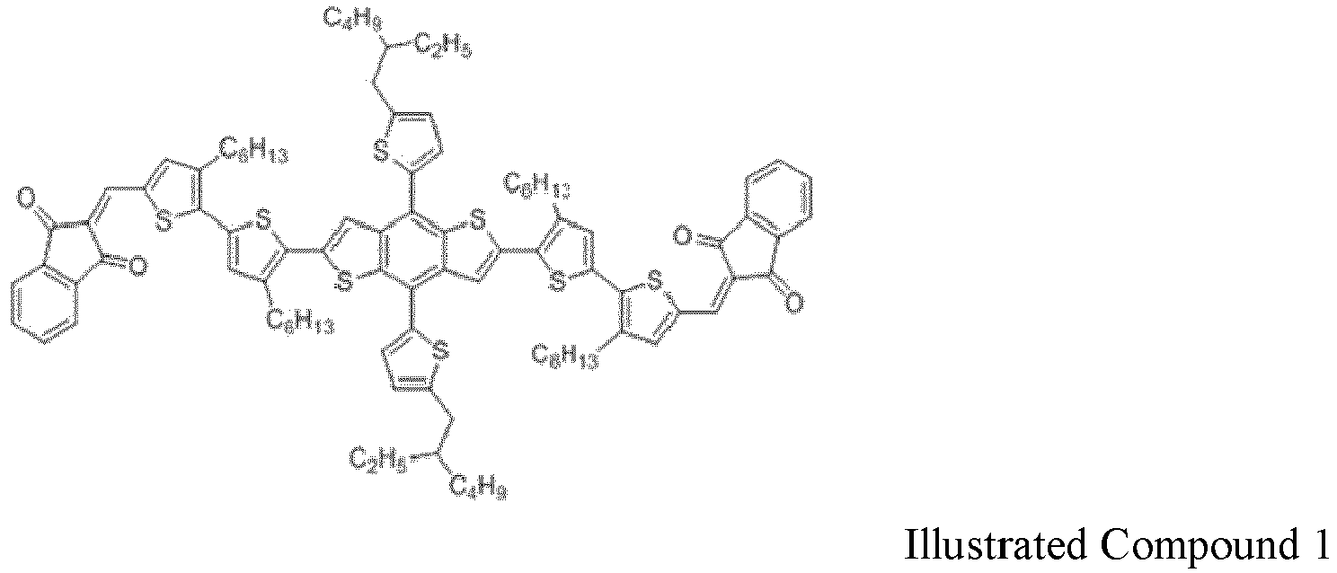

- The liquid application C of photoelectric conversion layer was spin-coated on the electron transport layer at 600 rpm to form a photoelectric conversion layer having an average thickness of 150 nm (T).
- Using a coherence scanning interferometer (VS1550, manufactured by Hitachi, Ltd.), the difference between the average thickness and the minimum thickness of the photoelectric conversion layer in the effective power generation region was found to be approximately 40 nm.
- A photoelectric converter was prepared in the same manner as in Example 3 except that an electron transport layer, a photoelectric transduction layer, a hole transport layer, a second electrode, and an insulating layer were formed in the following manner followed by sealing.
- A liquid of zinc oxide nano particles (average particle diameter of 12 nm (D), manufactured by Sigma-Aldrich Corporation) was spin-coated on an ITO filmed gas barrier PET film (15 Ω/□) at 1,000 rpm followed by drying at 120 degrees C for 10 minutes to form an electron transport layer having an average thickness of 40 nm.
- An ethanol solution of dimethylamino benzoate was prepared at a content of 1 mg/mL on the electron transport layer to form a film on the zinc oxide nano particles at 1,500 rpm. The number of foreign objects having a diameter of 100 nm or greater present in a region of 100 µm × 100 µm of the surface of the electron transport layer was found to be approximately 10 or less with coherence scanning interferometer (VS1550, manufactured by Hitachi, Ltd.). No further treatment was made.
- The liquid application C of photoelectric conversion layer was spin-coated on the electron transport layer at 600 rpm to form a photoelectric conversion layer having an average thickness of 150 nm (T).
- Using a coherence scanning interferometer (VS1550, manufactured by Hitachi, Ltd.), the difference between the average thickness and the minimum thickness of the photoelectric conversion layer in the effective power generation region was found to be approximately 30 nm.
- A hole transport layer of molybdenum oxide (manufactured by KOJUNDO CHEMICAL LABORATORY CO., LTD.) having a thickness of 20 nm and a second electrode made of gold having a thickness of 70 nm were sequentially vacuum deposited on the photoelectric conversion layer.
- A liquid dispersion of aluminium oxide nano particles (manufactured by Sigma-Aldrich Corporation) was spin-coated on the prepared photoelectric converter at 1,500 rpm so that a 300 nm insulating layer was formed.
- A sealing member on which an adhesive layer was formed on PET covered with aluminium was applied to the insulating layer of the photoelectric converter to cover the photoelectric converter using a roll laminator. The PET substrate in the photoelectric converter and the sealing member were attached to each other followed by sealing.
- A photoelectric converter was prepared in the same manner as in Example 4 except that the liquid application C of the photoelectric conversion layer was replaced with the following liquid application D of the photoelectric conversion layer.
- The difference between the average thickness and the minimum thickness of the photoelectric conversion layer in the effective power generation region was found to be approximately 60 nm in Example 5.
- A total of 15 mg of the
compound 1 illustrated above and 10 mg of PC61BM (E100H, manufactured by Frontier Carbon Corporation) were dissolved in 1 mL of chloroform to prepare the liquid dispersion D of photoelectric conversion layer. - A photoelectric converter was prepared in the same manner as in Example 4 except that the liquid application C of the photoelectric conversion layer was replaced with the following liquid application E of the photoelectric conversion layer.
- The difference between the average thickness and the minimum thickness of the photoelectric conversion layer in the effective power generation region was found to be approximately 40 nm in Example 6.
- The liquid application E of photoelectric conversion layer was prepared by dissolving 15 mg of the
compound 3 illustrated below (number average molecular weight (Mn) of 1,463) and 10 mg of thecompound 2 illustrated above in 1 mL of chloroform.
- A photoelectric converter was prepared in the same manner as in Example 4 except that the average thickness of the photoelectric conversion layer was changed to 100 nm (T).
- The difference between the average thickness and the minimum thickness of the photoelectric conversion layer in the effective power generation region was found to be approximately 40 nm in Example 7.
- A photoelectric converter was prepared in the same manner as in Example 4 except that the liquid dispersion of zinc oxide nano particles for use in forming the electron transport layer was changed to a liquid dispersion of zinc oxide nano particles (average particle diameter of 30 nm (D), manufactured by TAYCA CORPORATION) to form a photoelectric conversion layer having an average thickness of 230 nm (T).
- The number of foreign objects having a diameter of 100 nm or greater present in a region of 100 µm × 100 µm of the surface of the electron transport layer was found to be approximately 10 or less in Example 8. No further treatment was made. The difference between the average thickness and the minimum thickness of the photoelectric conversion layer in the effective power generation region was found to be approximately 30 nm.
- A photoelectric converter was prepared in the same manner as in Example 4 except that the average thickness (T) of the photoelectric conversion layer was changed to 310 nm.
- The difference between the average thickness and the minimum thickness of the photoelectric conversion layer in the effective power generation region was found to be approximately 60 nm in Example 9.
- A photoelectric converter was prepared in the same manner as in Example 4 except that the liquid application C of the photoelectric conversion layer was replaced with the following liquid application F of the photoelectric conversion layer.
- The difference between the average thickness and the minimum thickness of the photoelectric conversion layer in the effective power generation region was found to be approximately 40 nm in Example 10.
- The liquid application F of photoelectric conversion layer was prepared by dissolving 12.5 mg of the
compound 4 illustrated below (number average molecular weight (Mn) of 2,029) and 12.5 mg of thecompound 2 illustrated above in 1 mL of chloroform.
- A photoelectric converter was prepared in the same manner as in Example 4 except that the substrate with first electrode was replaced with the following substrate with first electrode.
- A glass substrate (10 Ω/□) on which ITO was formed was procured from Nippon Electric Glass Co., Ltd.
- Using a coherence scanning interferometer (VS1550, manufactured by Hitachi, Ltd.), the ITO was found to have a surface toughness Ra of approximately 5 nm.
- A photoelectric converter was prepared in the same manner as in Example 4 except that the electron transport layer was changed to the following and the average thickness of the photoelectric conversion layer was changed to 90 nm (T).
- The difference between the average thickness and the minimum thickness of the photoelectric conversion layer in the effective power generation region was found to be approximately 20 nm in Example 12.
- Aluminum-doped zinc oxide nano particle (average particle diameter of 12 nm (D), manufactured by Sigma-Aldrich Corporation) was spin-coated on an ITO filmed gas barrier PET film (15 Ω/□) at 1,000 rpm followed by drying at 120 degrees C for 10 minutes to form an electron transport layer having an average thickness of 40 nm.
- The number of foreign objects having a diameter of 100 nm or greater present in a region of 100 µm × 100 µm of the surface of the electron transport layer was found to be approximately 10 or less. No further treatment was made.
- A photoelectric converter was prepared in the same manner as in Example 4 except that the electron transport layer was changed to the following and the average thickness of the photoelectric conversion layer was changed to 70 nm (T).
- The difference between the average thickness and the minimum thickness of the photoelectric conversion layer in the effective power generation region was found to be approximately 20 nm in Example 13.
- Tin oxide nano particles (average particle diameter of 7 nm (D), manufactured by Sigma-Aldrich Corporation) were spin-coated on an ITO filmed gas barrier PET film (15 Ω/□) at 1,000 rpm followed by drying at 80 degrees C for 10 minutes to form an electron transport layer having an average thickness of 20 nm.
- The number of foreign objects having a diameter of 100 nm or greater present in a region of 100 µm × 100 µm of the surface of the electron transport layer was found to be approximately 10 or less. No further treatment was made.
- A photoelectric converter was prepared in the same manner as in Example 11 except that the electron transport layer was changed to the following.
- An ethanol liquid dispersion of zinc titanium nano particle paste (average particle diameter of 20 nm, manufactured by JGC Catalysts and Chemicals Ltd.) was spin-coated on an ITO filmed glass substrate (10 Ω/□, manufactured by Nippon Electric Glass Co., Ltd.) at 1,000 rpm followed by heating at 450 degrees C for 30 minutes to form an electron transport layer having an average thickness of 100 nm.
- The number of foreign objects having a diameter of 100 nm or greater present in a region of 100 µm × 100 µm of the surface of the electron transport layer was found to be approximately 10 or less. No further treatment was made.
- The difference between the average thickness and the minimum thickness of the photoelectric conversion layer in the effective power generation region was found to be approximately 30 nm in Example 14.
- A photoelectric converter was prepared in the same manner as in Example 4 except that the hole transport layer was changed to the following.
- Tungsten oxide (manufactured by KOJUNDO CHEMICAL LABORATORY CO., LTD.) was deposited onto the photoelectric conversion layer to form a hole transport layer having an average thickness of 20 nm.
- A photoelectric converter was prepared in the same manner as in Example 4 except that the hole transport layer was changed to the following.
- Vanadium oxide (manufactured by KOJUNDO CHEMICAL LABORATORY CO., LTD.) was deposited onto the photoelectric conversion layer to form a hole transport layer having an average thickness of 20 nm.
- A photoelectric converter was prepared in the same manner as in Example 4 except that the average thickness of the photoelectric conversion layer was changed to 470 nm (T).
- The difference between the average thickness and the minimum thickness of the photoelectric conversion layer in the effective power generation region was found to be approximately 50 nm in Example 17.
- A photoelectric converter was prepared in the same manner as in Example 4 except that the average thickness of the photoelectric conversion layer was changed to 550 nm (T).
- The difference between the average thickness and the minimum thickness of the photoelectric conversion layer in the effective power generation region was found to be approximately 50 nm in Example 18.
- A photoelectric converter was prepared in the same manner as in Example 4 except that the liquid dispersion of zinc oxide nano particles for use in forming the electron transport layer was changed to a liquid dispersion of zinc oxide nano particles (average particle diameter of 30 nm (D), manufactured by TAYCA CORPORATION).
- The number of foreign objects having a diameter of 100 nm or greater present in a region of 100 µm × 100 µm of the surface of the electron transport layer was found to be approximately 10 or less in Comparative Example 1. No further treatment was made.
- A photoelectric converter was prepared in the same manner as in Example 4 except that the average thickness of the photoelectric conversion layer was changed to 70 nm (T).
- The difference between the average thickness and the minimum thickness of the photoelectric conversion layer in the effective power generation region was found to be approximately 20 nm in Comparative Example 2.
- A photoelectric converter (Organic solar cell Module #3) was procured from InifinityPV ApS as the photoelectric converter of Comparative Example 3.
- The details of the material and the layer structure of the photoelectric converter of Comparative Example 3 are unavailable. The photoelectric converter of Comparative Example 3 had an extremely high density of current leakage. The density could not be precisely measured; it is, however, inferred that the ratio of current leakage was 0.99 or greater at an illuminance of 200 lux.
- Properties of the prepare photoelectric converters were evaluated in the following manner. The results are shown in Table 1.
- The highest occupied molecular orbital (HOMO) of the photoelectric conversion layer of the obtained photoelectric converter was measured using a photoemission yield spectroscopy in air (AC-2, manufactured by RIKEN KEIKI Co., Ltd.).
- The current-voltage of each of the obtained photoelectric converters were measured at an illuminance of white light emitting diode (LED) illumination of 100, 200, 2,000, 5,000, 10,000, and 18,000 lux.
- The white LED was a light-bulb form LED lamp (LDA11N G/100 W, manufactured by TOSHIBA Lighting & Technology Corporation). The current-voltage was measured using an evaluation device (source meter, KEYSIGHT B2902A).
- The illuminance of the white LED illumination was measured with an illuminometer (510 LUX METER, manufactured by Yokogawa Electric Corporation). The ratio PL of current leakage was obtained by the device evaluation and the current leakage ratio PL mentioned above using the density of short circuit current obtained at each illuminance and the values of open-circuit voltage.
- The ratio Pη of energy conversion efficiency was calculated between at 100 lux, low illuminance lower than 200 lux and a high illuminance of 20,000 lux according to the following equation (6):

- In the equation (6), η100 and η20000 respectively represent energy conversion efficiency at an illuminance of 100 lux and 20,000 lux of the light source.
- The ratio of the average particle diameter of the metal oxide particles and the average thickness of the photoelectric conversion layer were obtained for each photoelectric converter. The average particle diameter (D) of the metal oxide particle was measured as described above. The average thickness of the photoelectric conversion layer was measured according to the method described above.
Table 1 HOMO level of photoelectric conversion layer Ratio Pη of energy conversion efficiency Ratio PL of current leakage Average particle diameter (D) of metal oxide particle Average thickness (T) (nm) of photoelectric conversion layer Ratio (T/D) Example 1 4.9 eV 0.81 0.66 12 200 16.7 Example 2 5.1 eV 0.82 0.65 12 200 16.7 Example 3 5.2 eV 0.80 0.68 12 150 12.5 Example 4 5.2 eV 0.86 0.62 12 150 12.5 Example 5 5.2 eV 0.76 0.71 12 150 12.5 Example 6 5.3 eV 0.80 0.67 12 150 12.5 Example 7 5.2 eV 0.75 0.81 12 100 8.3 Example 8 5.2 eV 0.74 0.83 30 230 7.6 Example 9 5.2 eV 0.91 0.59 12 310 25.8 Example 10 5.3 eV 0.80 0.68 12 150 12.5 Example 11 5.2 eV 0.86 0.64 12 150 12.5 Example 12 5.2 eV 0.72 0.93 12 90 7.5 Example 13 5.2 eV 0.70 0.90 7 70 10.0 Example 14 5.2 eV 0.86 0.63 20 150 7.5 Example 15 5.2 eV 0.88 0.65 12 150 12.5 Example 16 5.2 eV 0.85 0.64 12 150 12.5 Example 17 5.2 eV 0.90 0.60 12 470 39.2 Example 18 5.2 eV 0.73 0.85 12 550 45.8 Comparative Example 1 5.2 eV 0.48 0.97 30 150 5.0 Comparative Example 2 5.2 eV 0.47 0.98 12 70 5.8 Comparative Example 3 - 0.12 > 0.99 - - - - As seen in the results shown in Table 1, every photoelectric converter of Examples 1 to 18 had a ratio PL of current leakage of 0.95 eV or less. The ratio of the energy conversion efficiency at a low illumination environment against the energy conversion efficiency in a high illumination environment was 70 percent or more; the photoelectric conversion efficiency at a low illumination environment does not significantly deteriorate in comparison with the photoelectric conversion efficiency in a high illumination environment.
- Conversely, the ratio PL of current leakage of the photoelectric converters of Comparative Examples 1 to 3 surpasses 0.95; the energy conversion efficiency in a low illumination environment is down more than 50 percent in comparison with the photoelectric conversion efficiency in a high illumination environment.
- Aspects of the present disclosure are, for example, as follows.
- 1. A photoelectric converter (1) includes a substrate (2), a first electrode (3) on the substrate (2), an electron transport layer (4) overlying the first electrode (3), a photoelectric conversion layer (5) overlying the first electrode (3), the photoelectric conversion layer (5) containing at least two types of organic materials, a hole transport layer (6) overlying the photoelectric conversion layer (5), and a second electrode (7) overlying the hole transport layer (6), wherein the photoelectric converter (1) has a ratio PL of current leakage of 0.95 or less at an illuminance of 200 lux, where the ratio PL is calculated from the following equation (1):

In the equation (1), L represents a density (µA/cm2) of current leakage at an illuminance of 200 lux and Jph represents a density (µA/cm2) of photocurrent at an illuminance of 200 lux. - 2. The photoelectric converter (1) according to 1 mentioned above, wherein the electron transport layer (4) contains metal oxide particles, wherein the following relationship is satisfied, 7.0 ≤ T/D, where T represents an average thickness of the photoelectric conversion layer (5) and D represents an average particle diameter of the metal oxide particles.
- 3. The photoelectric converter (1) according to 1 or 2 mentioned above, further comprising an insulating layer (8), wherein the first electrode (3) comprises a transparent electroconductive film.
- 4. The photoelectric converter (1) according to 2 or 3 mentioned above, wherein the metal oxide particles contain particles of zinc oxide, titanium oxide, or tin oxide.
- 5. The photoelectric converter (1) according to any one of 1 to 4 mentioned above, wherein the hole transport layer (6) comprises metal oxides selected from the group consisting of molybdenum oxide, tungsten oxide, and vanadium oxide.
- 6. The photoelectric converter (1) according to any one of 1 to 5 mentioned above, wherein one of the at least two types of organic materials comprises an electron donor having a highest occupied molecular orbital (HOMO) level of from 5.1 to 5.5 eV and a number average molecular weight (Mn) of 10,000 or less.
- 7. The photoelectric converter (1) according to any one of 1 to 6 mentioned above, wherein the one of the at least two types of organic materials is represented by a compound represented by the following Chemical Formula (1)


- 8. The photoelectric converter (1) according to 6 or 7 mentioned above, wherein the at least two types of organic materials excluding the one of the at least two types of organic materials comprise fullerene derivatives.
- 9. The photoelectric converter (1) according to any one of 1 to 8 mentioned above, wherein the electron transport layer (4) comprises a first electron transport layer containing metal oxide particles and a second electron transport layer between the first electron transport layer and the photoelectric conversion layer (5), wherein the second electron transport layer contains an amine compound represented by the following Chemical Formula (4)

- 10. A photoelectric converter module includes the photoelectric converters (1) of any one of 1 to 9 mentioned above which are connected in series or parallel.
- 11. An electronic device includes one or both of the photoelectric converter (1) of any one of
claims 1 to 9, the photoelectric converter module of 10 mentioned above, and a device configured to operate on electricity generated by photoelectric conversion by the one or both of the photoelectric converter and the photoelectric converter module. - 12. An electronic device includes one or both of the photoelectric converter (1) of any one of
claims 1 to 9, the photoelectric converter module of 10 mentioned above, and a rechargeable battery configured to store electricity generated by photoelectric conversion by the one or both of the photoelectric converter (1) and the photoelectric converter module, and a device configured to operate on the electricity generated by photoelectric conversion by the one or both of the photoelectric converter (1) and the photoelectric converter module or stored in the rechargeable battery. - 13. A power source module includes one or both of the photoelectric converter (1) of any one of 1 to 9 mentioned above and the photoelectric converter module of 10 mentioned above; and a power control IC.
- Numerous additional modifications and variations are possible in light of the above teachings. It is therefore to be understood that, within the scope of the above teachings, the present disclosure may be practiced otherwise than as specifically described herein. With some embodiments having thus been described, it will be obvious that the same may be varied in many ways. Such variations are not to be regarded as a departure from the scope of the present disclosure and appended claims, and all such modifications are intended to be included within the scope of the present disclosure and appended claims.
Claims (13)
- A photoelectric converter (1) comprising:a substrate (2);a first electrode (3) on the substrate (2);an electron transport layer (4) overlying the first electrode (3);a photoelectric conversion layer (5) overlying the electron transport layer (4), the photoelectric conversion layer (5) containing at least two types of organic materials;a hole transport layer (6) overlying the photoelectric conversion layer (5); anda second electrode (7) overlying the hole transport layer (6),wherein the photoelectric converter (1) has a ratio PL of current leakage of 0.95 or less at an illuminance of 200 lux, where the ratio PL is calculated from the following equation (1):

where L represents a density (µA/cm2) of current leakage at an illuminance of 200 lux and Jph represents a density (µA/cm2) of photocurrent density at an illuminance of 200 lux. - The photoelectric converter (1) according to claim 1,
wherein the electron transport layer (4) comprises metal oxide particles, wherein the following relationship is satisfied, 7.≤ T/D, where T represents an average thickness of the photoelectric conversion layer (5) and D represents an average particle diameter of the metal oxide particles. - The photoelectric converter (1) according to claim 1 or 2, further comprising an insulating layer (8), wherein the first electrode (3) comprises a transparent electroconductive film.
- The photoelectric converter (1) according to claim 2 or 3, wherein the metal oxide particles comprise particles of zinc oxide, titanium oxide, or tin oxide.
- The photoelectric converter (1) according to any one of claims 1 to 4, wherein the hole transport layer (6) comprises molybdenum oxide, tungsten oxide, or vanadium oxide.
- The photoelectric converter (1) according to any one of claims 1 to 5, wherein one of the at least two types of organic materials comprises an electron donor having a highest occupied molecular orbital (HOMO) level of from 5.1 to 5.5 eV and a number average molecular weight (Mn) of 10,000 or less.
- The photoelectric converter (1) according to any one of claims 1 to 6, wherein one of the at least two types of organic materials comprises a compound represented by the following Chemical Formula (1):


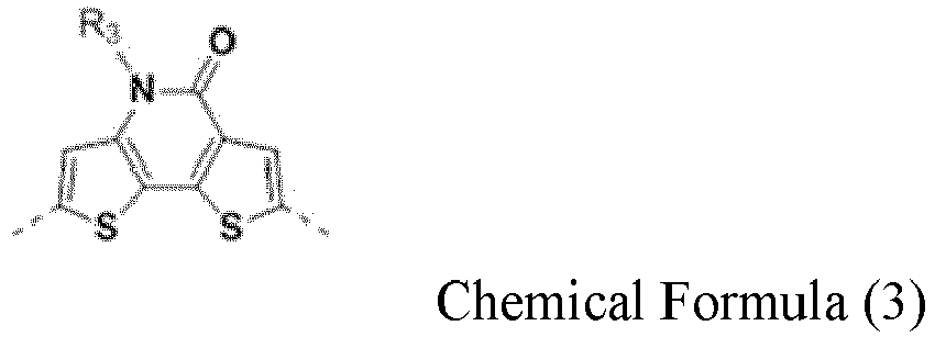
- The photoelectric converter (1) according to claim 6 or 7, wherein the at least two types of organic materials excluding the one of the at least two types of organic materials comprise fullerene derivatives.
- The photoelectric converter (1) according to any one of claims 1 to 8,
wherein the electron transport layer (4) comprises a first electron transport layer containing metal oxide particles and a second electron transport layer between the first electron transport layer and the photoelectric conversion layer (5),
wherein the second electron transport layer comprises an amine compound represented by the following Chemical Formula (4)
- A photoelectric converter module comprising:
the photoelectric converters (1) of any one of claims 1 to 9 which are connected in series or parallel. - An electronic device comprising:one or both of the photoelectric converter (1) of any one of claims 1 to 9 and the photoelectric converter module of claim 10; anda device configured to operate on electricity generated by photoelectric conversion by the one or both of the photoelectric converter (1) and the photoelectric converter module.
- An electronic device comprising:one or both of the photoelectric converter (1) of any one of claims 1 to 9 and the photoelectric converter module of claim 10; anda rechargeable battery configured to store electricity generated by photoelectric conversion by the one or both of the photoelectric converter (1) and the photoelectric converter module; anda device configured to operate on the electricity generated by photoelectric conversion by the one or both of the photoelectric converter (1) and the photoelectric converter module or stored in the rechargeable battery.
- A power source module comprising:one or both of the photoelectric converter (1) of any one of claims 1 to 9 and the photoelectric converter module of claim 10; anda power control IC.
Applications Claiming Priority (1)
| Application Number | Priority Date | Filing Date | Title |
|---|---|---|---|
| JP2020008114A JP2021118190A (en) | 2020-01-22 | 2020-01-22 | Photoelectric conversion element, photoelectric conversion element module, electronic device, and power supply module |
Publications (1)
| Publication Number | Publication Date |
|---|---|
| EP3855523A1 true EP3855523A1 (en) | 2021-07-28 |
Family
ID=74191615
Family Applications (1)
| Application Number | Title | Priority Date | Filing Date |
|---|---|---|---|
| EP21152355.0A Withdrawn EP3855523A1 (en) | 2020-01-22 | 2021-01-19 | Photoelectric converter, photoelectric conversion module, electronic device, and power source module |
Country Status (2)
| Country | Link |
|---|---|
| EP (1) | EP3855523A1 (en) |
| JP (1) | JP2021118190A (en) |
Cited By (3)
| Publication number | Priority date | Publication date | Assignee | Title |
|---|---|---|---|---|
| WO2023058490A1 (en) * | 2021-10-07 | 2023-04-13 | Ricoh Company, Ltd. | Photoelectric conversion device, electronic device, and power supply module |
| US20230171975A1 (en) * | 2021-11-26 | 2023-06-01 | Yuuji Tanaka | Photoelectric conversion element, photoelectric conversion module, electronic device, and partition |
| US20240097612A1 (en) * | 2022-09-21 | 2024-03-21 | The Regents Of The University Of Michigan | Organic optoelectronic device and method |
Families Citing this family (1)
| Publication number | Priority date | Publication date | Assignee | Title |
|---|---|---|---|---|
| JP2022085070A (en) | 2020-11-27 | 2022-06-08 | 株式会社リコー | Photoelectric conversion module, electronic equipment, and power supply module |
Citations (4)
| Publication number | Priority date | Publication date | Assignee | Title |
|---|---|---|---|---|
| JP2014220333A (en) | 2013-05-07 | 2014-11-20 | Jx日鉱日石エネルギー株式会社 | Method of manufacturing photoelectric conversion element and photoelectric conversion element |
| JP2016208568A (en) | 2015-04-15 | 2016-12-08 | シャープ株式会社 | Mobile electronic apparatus case |
| US20180342701A1 (en) * | 2017-05-26 | 2018-11-29 | Osram Oled Gmbh | Organic Optoelectronic Component |
| WO2019176488A1 (en) * | 2018-03-15 | 2019-09-19 | Ricoh Company, Ltd. | Organic material and photoelectric conversion element |
-
2020
- 2020-01-22 JP JP2020008114A patent/JP2021118190A/en active Pending
-
2021
- 2021-01-19 EP EP21152355.0A patent/EP3855523A1/en not_active Withdrawn
Patent Citations (4)
| Publication number | Priority date | Publication date | Assignee | Title |
|---|---|---|---|---|
| JP2014220333A (en) | 2013-05-07 | 2014-11-20 | Jx日鉱日石エネルギー株式会社 | Method of manufacturing photoelectric conversion element and photoelectric conversion element |
| JP2016208568A (en) | 2015-04-15 | 2016-12-08 | シャープ株式会社 | Mobile electronic apparatus case |
| US20180342701A1 (en) * | 2017-05-26 | 2018-11-29 | Osram Oled Gmbh | Organic Optoelectronic Component |
| WO2019176488A1 (en) * | 2018-03-15 | 2019-09-19 | Ricoh Company, Ltd. | Organic material and photoelectric conversion element |
Non-Patent Citations (3)
| Title |
|---|
| APPLIED PHYSICS LETTERS, vol. 108, no. 253301, 2016 |
| JAPANESE JOURNAL OF APPLIED PHYSICS, vol. 54, no. 071602, 2015 |
| PARK SUNG-HYUN ET AL: "Large area roll-to-roll sputtering of transparent ITO/Ag/ITO cathodes for flexible inverted organic solar cell modules", ORGANIC ELECTRONICS, ELSEVIER, AMSTERDAM, NL, vol. 30, 28 December 2015 (2015-12-28), pages 112 - 121, XP029403578, ISSN: 1566-1199, DOI: 10.1016/J.ORGEL.2015.12.009 * |
Cited By (3)
| Publication number | Priority date | Publication date | Assignee | Title |
|---|---|---|---|---|
| WO2023058490A1 (en) * | 2021-10-07 | 2023-04-13 | Ricoh Company, Ltd. | Photoelectric conversion device, electronic device, and power supply module |
| US20230171975A1 (en) * | 2021-11-26 | 2023-06-01 | Yuuji Tanaka | Photoelectric conversion element, photoelectric conversion module, electronic device, and partition |
| US20240097612A1 (en) * | 2022-09-21 | 2024-03-21 | The Regents Of The University Of Michigan | Organic optoelectronic device and method |
Also Published As
| Publication number | Publication date |
|---|---|
| JP2021118190A (en) | 2021-08-10 |
Similar Documents
| Publication | Publication Date | Title |
|---|---|---|
| WO2020026752A1 (en) | Photoelectric conversion element, photoelectric conversion element module, organic thin-film solar cell, electronic apparatus, and power supply module | |
| Han et al. | 12.42% Monolithic 25.42 cm2 flexible organic solar cells enabled by an amorphous ITO‐modified metal grid electrode | |
| JP2021118190A (en) | Photoelectric conversion element, photoelectric conversion element module, electronic device, and power supply module | |
| EP4064376B1 (en) | Photoelectric conversion element | |
| Ding et al. | Characterizing and improving the thermal stability of organic photovoltaics based on halogen-rich non-fullerene acceptors | |
| US12041797B2 (en) | Photoelectric conversion element, device, and power supply module | |
| Gao et al. | Redefining PbS Quantum Dot Photovoltaics: p‐i‐n Devices with Superior Efficiency and Reproducibility | |
| EP4006979B1 (en) | Photoelectric conversion module, electronic device, and power supply module | |
| US20230232642A1 (en) | Photoelectric conversion element, photoelectric conversion element module, electronic device, power supply module, and method for producing photoelectric conversion element | |
| EP4006978A1 (en) | Photoelectric conversion module, electronic device, and power supply module | |
| EP4413601B1 (en) | Photoelectric conversion device, electronic device, and power supply module | |
| EP4315447B1 (en) | Photoelectric conversion element, photoelectric conversion module, electronic device, and power supply module | |
| TWI709257B (en) | Flexible perovskite solar cell and manufacturing method thereof | |
| Qasim et al. | Fabrication and characterization of bulk heterojunction organic solar cell: a review | |
| Hatton | Organic Photovoltaics | |
| EP4131445B1 (en) | Photoelectric conversion device, electronic device, and power supply module | |
| Saravanapavanantham | Large-area lightweight organic photovoltaics |
Legal Events
| Date | Code | Title | Description |
|---|---|---|---|
| PUAI | Public reference made under article 153(3) epc to a published international application that has entered the european phase |
Free format text: ORIGINAL CODE: 0009012 |
|
| STAA | Information on the status of an ep patent application or granted ep patent |
Free format text: STATUS: REQUEST FOR EXAMINATION WAS MADE |
|
| 17P | Request for examination filed |
Effective date: 20210119 |
|
| AK | Designated contracting states |
Kind code of ref document: A1 Designated state(s): AL AT BE BG CH CY CZ DE DK EE ES FI FR GB GR HR HU IE IS IT LI LT LU LV MC MK MT NL NO PL PT RO RS SE SI SK SM TR |
|
| STAA | Information on the status of an ep patent application or granted ep patent |
Free format text: STATUS: EXAMINATION IS IN PROGRESS |
|
| 17Q | First examination report despatched |
Effective date: 20230626 |
|
| STAA | Information on the status of an ep patent application or granted ep patent |
Free format text: STATUS: THE APPLICATION HAS BEEN WITHDRAWN |
|
| 18W | Application withdrawn |
Effective date: 20230925 |