EP3855509A1 - Partially translucent photovoltaic window and method of manufacturing the same - Google Patents
Partially translucent photovoltaic window and method of manufacturing the same Download PDFInfo
- Publication number
- EP3855509A1 EP3855509A1 EP20153934.3A EP20153934A EP3855509A1 EP 3855509 A1 EP3855509 A1 EP 3855509A1 EP 20153934 A EP20153934 A EP 20153934A EP 3855509 A1 EP3855509 A1 EP 3855509A1
- Authority
- EP
- European Patent Office
- Prior art keywords
- photovoltaic
- window
- layer
- window pane
- perovskite
- Prior art date
- Legal status (The legal status is an assumption and is not a legal conclusion. Google has not performed a legal analysis and makes no representation as to the accuracy of the status listed.)
- Withdrawn
Links
Images



Classifications
-
- H—ELECTRICITY
- H10—SEMICONDUCTOR DEVICES; ELECTRIC SOLID-STATE DEVICES NOT OTHERWISE PROVIDED FOR
- H10K—ORGANIC ELECTRIC SOLID-STATE DEVICES
- H10K85/00—Organic materials used in the body or electrodes of devices covered by this subclass
- H10K85/50—Organic perovskites; Hybrid organic-inorganic perovskites [HOIP], e.g. CH3NH3PbI3
-
- B—PERFORMING OPERATIONS; TRANSPORTING
- B32—LAYERED PRODUCTS
- B32B—LAYERED PRODUCTS, i.e. PRODUCTS BUILT-UP OF STRATA OF FLAT OR NON-FLAT, e.g. CELLULAR OR HONEYCOMB, FORM
- B32B17/00—Layered products essentially comprising sheet glass, or glass, slag, or like fibres
-
- H—ELECTRICITY
- H02—GENERATION; CONVERSION OR DISTRIBUTION OF ELECTRIC POWER
- H02S—GENERATION OF ELECTRIC POWER BY CONVERSION OF INFRARED RADIATION, VISIBLE LIGHT OR ULTRAVIOLET LIGHT, e.g. USING PHOTOVOLTAIC [PV] MODULES
- H02S20/00—Supporting structures for PV modules
- H02S20/20—Supporting structures directly fixed to an immovable object
- H02S20/22—Supporting structures directly fixed to an immovable object specially adapted for buildings
- H02S20/26—Building materials integrated with PV modules, e.g. façade elements
-
- H—ELECTRICITY
- H10—SEMICONDUCTOR DEVICES; ELECTRIC SOLID-STATE DEVICES NOT OTHERWISE PROVIDED FOR
- H10F—INORGANIC SEMICONDUCTOR DEVICES SENSITIVE TO INFRARED RADIATION, LIGHT, ELECTROMAGNETIC RADIATION OF SHORTER WAVELENGTH OR CORPUSCULAR RADIATION
- H10F19/00—Integrated devices, or assemblies of multiple devices, comprising at least one photovoltaic cell covered by group H10F10/00, e.g. photovoltaic modules
- H10F19/80—Encapsulations or containers for integrated devices, or assemblies of multiple devices, having photovoltaic cells
-
- H—ELECTRICITY
- H10—SEMICONDUCTOR DEVICES; ELECTRIC SOLID-STATE DEVICES NOT OTHERWISE PROVIDED FOR
- H10K—ORGANIC ELECTRIC SOLID-STATE DEVICES
- H10K30/00—Organic devices sensitive to infrared radiation, light, electromagnetic radiation of shorter wavelength or corpuscular radiation
- H10K30/40—Organic devices sensitive to infrared radiation, light, electromagnetic radiation of shorter wavelength or corpuscular radiation comprising a p-i-n structure, e.g. having a perovskite absorber between p-type and n-type charge transport layers
-
- H—ELECTRICITY
- H10—SEMICONDUCTOR DEVICES; ELECTRIC SOLID-STATE DEVICES NOT OTHERWISE PROVIDED FOR
- H10K—ORGANIC ELECTRIC SOLID-STATE DEVICES
- H10K50/00—Organic light-emitting devices
- H10K50/80—Constructional details
- H10K50/84—Passivation; Containers; Encapsulations
- H10K50/846—Passivation; Containers; Encapsulations comprising getter material or desiccants
Definitions
- the invention relates to a partially translucent photovoltaic window.
- the present invention further relates to a method of manufacturing a partially translucent photovoltaic window.
- Perovskites are promising materials for application in photovoltaic devices as they facilitate low temperature manufacturing conditions have a relatively high conversion efficiency.
- a relatively new application is the incorporation of photovoltaic devices in a window. Therewith it can serve to absorb solar radiation for attenuation while at the same time converting the solar radiation into useful electrical energy. It is however a potential risk that in case the window is damaged, water can penetrate therein, dissolve solid state lead compounds to form Pb 2+ which is therewith distributed, which is an environmental and health risk.
- a partially translucent photovoltaic window that is improved in accordance with the first mentioned object is defined in claim 1.
- the improved partially translucent photovoltaic window comprises a photovoltaic module enclosed between a first window pane and a second window pane.
- the photovoltaic module comprises a stack with at least a first electrode layer, a second electrode layer and a perovskite photovoltaic layer between said electrode layers.
- the photovoltaic window further comprises a first intermediate layer containing a lead getter material.
- the partially translucent photovoltaic window comprises a second intermediate layer containing a lead getter material.
- the lead getter material comprises one or more of sulphur or phosphor. Therewith lead is immobilized by conversion into insoluble leadsulfide or leadphosphate before it can penetrate through the intermediate layer.
- the window is partially translucent, in that a portion (e.g. at least 30%) of incident radiation is transmitted and another portion of the incident radiation is absorbed in the perovskite photovoltaic layer for conversion into electrical energy.
- the portion absorbed for conversion may for example have a substantially uniform distribution over the visible spectrum. Therewith, perception of colors in a scene through the window is substantially the same as it would be in the absence of the window.
- the portion absorbed for conversion may have a non-uniform distribution over the visible spectrum.
- the photovoltaic window radiation having a wavelength in the range of 500-600 nm may be almost completely absorbed for conversion into electric energy, whereas radiation outside this range may be substantially transmitted.
- radiation in the subranges of 350-500 nm and 600-700 nm, which is important for photosynthesis is substantially transmitted.
- the portion absorbed for conversion may have a non-uniform spectral distribution in that in particular solar radiation having a relative wavelength, e.g. more than 700 nm is strongly absorbed for conversion.
- a photovoltaic window of this type may serve for example in buildings to mitigate heating by solar radiation.
- incident light is optimally used for illumination of a room and for conversion into electrical energy
- all elements of the photovoltaic window other than the perovskite photovoltaic layer are substantially translucent, e.g. in that at most 10% of incoming radiation is absorbed anywhere in these layers on its way through the window.
- the photovoltaic window is also transparent, to enable vision through the window.
- the window is merely partially translucent, but not transparent. In that case it may have the appearance of frosted glass. For application in greenhouses as specified above, this will often be sufficient. Also in buildings such translucent, non-transparent windows may serve where access of solar light is required but transparency is not required in view of privacy.
- At least one of the respective intermediate layers is of an elastic polymer, which has the lead getter material dispersed therein.
- the elastic polymer reduces the risk of damage, and/or minimizes the impact of damage to the window by maintain integrity. Therewith a synergic effect is achieved in that the intermediate layer serves a dual purpose. When maintaining integrity in a damaged window penetration of water is mitigated. Also outward diffusion of water is mitigated therewith increasing a time of contact between the dissolved lead compounds and the lead getter material.
- a method of manufacturing the improved partially translucent photovoltaic window is specified in claim 10.
- the improved method of manufacturing provides the partially translucent photovoltaic window as a layered product.
- the layered product subsequently comprises:
- embodiments of the invention should not be construed as limited to the particular shapes of regions illustrated herein but are to include deviations in shapes that result, for example, from manufacturing.
- the regions illustrated in the figures are schematic in nature and their shapes are not intended to illustrate the actual shape of a region of a device and are not intended to limit the scope of the invention.
- FIG. 1 schematically shows a partially translucent photovoltaic window 1 that comprises a photovoltaic module 4 enclosed between a first window pane 2 and a second window pane 6.
- the photovoltaic module 4 comprises a stack with at least a first electrode layer 41 (here a cathode), a second electrode layer 45 (anode) and a perovskite photovoltaic layer 43 between said electrode layers.
- a first electrode layer 41 here a cathode
- second electrode layer 45 anode
- a perovskite photovoltaic layer 43 between said electrode layers.
- an electron transport layer 42 is provided between the first electrode layer 41 and the photovoltaic layer 43.
- a hole transport layer 44 is provided between the second electrode layer 45 and the photovoltaic layer 43.
- the photovoltaic window 1 further comprises a first intermediate layer 3 between the first window pane 2 and the photovoltaic module 4.
- the photovoltaic window 1 still further comprises a second intermediate layer 5 between the second window pane 6 and the photovoltaic module 4.
- the first and the second intermediate layer 3,5 comprise a lead getter material.
- the first and the second electrode layer 41, 45 of the photovoltaic module 4 are connected via electric conductors 11, 12 to a power converter 10 that is connected via a further set of conductors 13, 14, 15 to a mains network.
- daylight R1 is partly absorbed and converted into electrical energy and delivered by the power converter 10 via the further set of conductors 13, 14, 15 to the mains network.
- the generated electrical energy may be used in a local DC network, for example to charge battery.
- a portion R2 of the daylight R1 protrudes through the partially translucent photovoltaic window 1 so as to serve as an attenuated illumination of an interior.
- all parts of the partially translucent photovoltaic window 1, except the perovskite photovoltaic layer 43 are typically highly translucent.
- the window panes 2, 6 may be provided of a glass which is conventional in window applications and electrode layers 41, 45, the electron transport layer 42, the hole transport layer 44, as well as the intermediate layers 3, 5 are highly translucent, e.g. preferably have a translucency in the visible wavelength range of at least 50%. That is to say that at least half of the total solar power within a wavelength range of about 380 to about 740 nm impingent on the photovoltaic window reaches the photovoltaic layer 43. More preferably the translucency is at least 75% and still more preferably it is at least 90%.
- the partially translucent photovoltaic window 1 may be transparent, but in some applications that is not necessary or may not be desired.
- additional layers may be present, as sublayers of the above-mentioned layers, or as additional layers.
- a further electro-optical layer stack may for example serve to allow a user to electrically control a transparency of the partially translucent photovoltaic window 1. This allows the user to change an appearance of the window 1 between transparent and opal, or in an intermediate state.
- an electro-optical layer stack may serve for conversion of electrical energy into light. Therewith the window 1 can serve as an active source of light in the absence of daylight. Also combinations of various electro-optical layer stacks may be provided.
- the window panes 2, 6 may be of any glass which is known for use in conventional windows.
- the panes may for example have a thickness of a few mm.
- one or both window panes 2, 6 may made of a resin such as polyethylene terephthalate (PET), polyethylene naphthalate (PEN), polyimide (PI), polyetherimide (PEI), polyethersulfone (PES), polysulfone (PSF), polyphenylene sulfide (PPS), polyether ether ketone (PEEK), polyarylate (PAR), and polyamide-imide (PAI).
- PET polyethylene terephthalate
- PEN polyethylene naphthalate
- PI polyimide
- PEI polyetherimide
- PES polyethersulfone
- PSF polyphenylene sulfide
- PES polyether ether ketone
- PAR polyarylate
- PAI polyamide-imide
- resin materials include polycycloolefin resin, acrylic resin, polystyrene, ABS, polyethylene, polypropylene, polyamide resin, polyvinyl chloride resin, polycarbonate resin, polyphenyleneether resin and cellulose resin, etc.
- a resin is used for the window panes 2, 6, it may be contemplated to provide these with a (moisture, oxygen) barrier coating, for example comprising one or more inorganic layers.
- Such resin materials may also be contemplated as a matrix for the intermediate layers 3, 5.
- a lead getter material may be dispersed therein as finely distributed particles, e.g. Sulphur or phosphor particles.
- the perovskite materials therein typically have a crystal structure of ABX 3 , wherein A is an organic cation as methylammonium (CH 3 NH 3 ) + , B is an inorganic cation, usually lead (II) (Pb 2+ ), and X is a halogen atom such as iodine (I-), chlorine (Cl-), fluorine (F-) or bromine (Br-).
- Perovskite materials are particularly advantageous in that they can be processed relatively easily and in that their bandgap can be set to a desired value by a proper choice of the halide content.
- methylammonium lead trihalide (CH 3 NH 3 PbX 3 ), with an optical bandgap between 1.5 and 2.3 eV depending on halide content.
- Other more complex structures contain mixed A cations, such as Cesium (Cs+), methylammonium ((CH 3 NH 3 )+, MA), formamidinum ((H 2 NCHNH 2 )+, FA), or rubidium (Rb+) and mixed X anions.
- the examples of complex mixed perovskites are Cesium formamidinum lead trihalide Cs x FA 1-x PbI y Br 3-y and Cesium Methylamonium formamidinum lead trihalide Cs x MA z FA 1-x-z PbI y Br 3-y (where x ⁇ 1, z ⁇ 1, x+z ⁇ 1).
- Cs x MA z FA 1-x-z PbI y Br 3-y where x ⁇ 1, z ⁇ 1, x+z ⁇ 1
- Other metals such as tin may replace the role of Pb in the B position of perovskite materials.
- An example thereof is CH 3 NH 3 SnI 3 .
- a perovskite photovoltaic layer 43 may have a thickness in the range of 100 nm to 20 micron for example.
- a translucent electrically conductive material for use in the first and the second electrode layers 41, 45 may be of an organic or an inorganic nature.
- organic translucent (transparent) electrically conductive materials are polyaniline, polythiophene, polypyrrole or doped polymers.
- inorganic translucent (transparent) electrically conductive materials are ITO (Indium Tin Oxide), IZO (Indium Zinc Oxide), ATO (Antimony Tin Oxide), or Tin Oxide can be used.
- ITO Indium Tin Oxide
- IZO Indium Zinc Oxide
- ATO Antimony Tin Oxide
- Tin Oxide can be used.
- Other metal oxides can work, including but not limited to Nickel-Tungsten-Oxide, Indium doped Zinc Oxide, Magnesium-Indium-Oxide.
- a TCO or a metal oxide layer or a conducting polymer layer, such as PEDOT-PSS may be used.
- a 7 nm layer of Silver may be sandwiched in between two 10 nm ITO layers.
- the transparent electrically conductive electrode layer may have a total thickness in the range of a few tens of nm to a few hundreds of nm, for example in a range between 100 and 200 nm, for example about 120 nm.
- a hole transport layer here the charge carrier transport layer 44, such as a nickel-oxide layer or a MoSe layer, may be provided between the anode (here layer 45) and the photovoltaic layer 43.
- the charge carrier transport layer 44 such as a nickel-oxide layer or a MoSe layer
- the charge carrier transport layer 45 may be provided between the anode (here layer 45) and the photovoltaic layer 43.
- hole transport materials for a hole transport layer have been summarized for example, in Kirk-Othmer Encyclopedia of Chemical Technology, Fourth Edition, Vol. 18, p. 837-860, 1996, by Y. Wang . Both hole transporting molecules and polymers can be used.
- a hole transport layer may have a thickness in the range of 10 to 200 nm.
- an electron transport layer here the layer 42 may be provided between the cathode (here 41) and the photovoltaic layer 43.
- Suitable materials for this purpose are for example TiO 2 , SnO 2 , ZrO 2 and ZnO:
- the electron transport layer may have a thickness in the range of a few nm to a few tens of nm.
- FIG. 2A shows an exceptional case wherein the window is damaged, for example due to a hailstone H incident on window pane 6.
- water W could penetrate trough the damaged portion of the window pane 6 into the photovoltaic module 4.
- Solid state lead compound in the form of perovskite crystals or potentially by products like PbI 2 could then dissolve in the penetrated water to form Pb 2+ ions.
- phosphor may be provided as the lead getter material.
- Dissolved lead ions or lead containing ions in contact therewith react to insoluble leadphosphate and are therewith immobilized.
- Sulphur may be provided as the lead getter material. The latter immobilizes lead components as insoluble leadsulfides. Also combinations of lead getter materials may be used.
- the dissolved Pb 2+ ions react with a monohydrogen-phosphate to form an insoluble phosphate compound as follows. 5Pb 2+ + 3HPO 4 2- + X- ⁇ Pb 5 (PO 4 ) 3 X (s) + 3H +
- the negative ion X- is for example one of OH - ,F - ,Cl - , so that the insoluble reaction product is leadhydroxyphosphate (Pb 5 (PO 4 ) 3 OH), leadchlorophosphate (Pb 5 (PO 4 ) 3 Cl) or leadfluorophosphate (Pb 5 (PO 4 ) 3 Cl).
- the negative ion X - is for example one of OH - ,F - ,Cl - , so that the insoluble reaction product is leadhydroxyphosphate (Pb 5 (PO 4 ) 3 OH), leadchlorophosphate (Pb 5 (PO 4 ) 3 Cl) or leadfluorophosphate (Pb 5 (PO 4 ) 3 Cl).
- the dissolved Pb 2+ ions react with a sulphide ions S 2- to form insoluble leadsulphide as follows. Pb 2+ + S 2- ⁇ PbS.
- the intermediate layers 3, 5 are of an elastic polymer.
- the lead getter material is dispersed therein as particles, e.g. nanometer sized particles.
- the embodiment wherein at least one of the intermediate layers 3, 5 is provided as an elastic polymer helps to prevent a damage of the window 1 or in case a damage does occur, helps to maintain integrity of the window 1, so that removal of a damaged window is more easy.
- the elastic polymer is an adhesive.
- One example thereof is Polyvinyl butyral (or PVB) .
- FIG. 3A-3C schematically show a method of manufacturing a partially translucent photovoltaic window 1 as a layered product.
- the method comprises a step S2 wherein a first window pane 2 is provided.
- the first window pane 2 here serves as a substrate on which subsequently a stack of layers is provided.
- a first intermediate layer 3 comprising a lead getter material is provided on the first window pane 2.
- layers of a photovoltaic module 4 are provided.
- step S4 comprises sub-steps S41-S45 as follows.
- a first electrode layer 41 for example a cathode, is provided on the first intermediate layer 3.
- a first charge carrier transport layer 42 for example an electron transport layer is provided on the first electrode layer 41.
- a perovskite photovoltaic layer 43 is provided on the first charge carrier transport layer 42.
- a second charge carrier transport layer 44 for example a hole transport layer is provided on the perovskite photovoltaic layer 43.
- a second electrode layer 45 for example an anode, is provided on the second charge carrier transport layer 44.
- step S5 a second intermediate layer 5 comprising a lead getter material is provided on the photovoltaic module 4.
- Various technologies are available for providing a layer in the steps referred to above.
- Various methods may be used for depositing and applying layers.
- Example of these methods may include spin-coating, printing methods, slot-die coating and vapor deposition methods like physical vapor deposition (e.g. E-beam PVD, Sputter PVD), (spatial) Atomic Layer Deposition ((s)ALD) and the like.
- FIG. 4A, 4B Another exemplary method of manufacturing is depicted in FIG. 4A, 4B .
- FIG. 4A shows a preparatory step S4 having sub-steps S41-S45 as shown in FIG. 3C , wherein a photovoltaic module 4 is provided that comprises a stack with at least a first electrode layer 41, a second electrode layer 45 and a perovskite photovoltaic layer 43 between said electrode layers.
- a photovoltaic module 4 is provided that comprises a stack with at least a first electrode layer 41, a second electrode layer 45 and a perovskite photovoltaic layer 43 between said electrode layers.
- the first window pane 2 having the first intermediate layer 3 is provided and in preparatory sub-step S12, the first window pane 6 having the second intermediate layer 5 is provided.
- subsequent step S13 the intermediary products obtain in preparatory steps S4, S11 and S12 are laminated into the partially translucent photovoltaic window 1 shown in FIG. 4B .
- FIG. 5 schematically shows a greenhouse 20 provided with a roof 21 formed by partially translucent photovoltaic windows 1 as shown in FIG. 1 , or being covered therewith.
- the greenhouse 20 shown in FIG. 3 encloses an inner space 22 for growing plants 23.
- the photovoltaic windows 1 comprised in the roof 21, or from which the roof is constructed has a photovoltaic module 4, wherein the perovskite photovoltaic layer 43 has a relative high absorption for radiation with a wavelength in the range of 500-600 nm, and has a relatively low absorption radiation for visible radiation outside this range.
- FIG. 6 schematically shows a house 30 having a roof 31, front door 32, windows 33, 34 and further having an embodiment of partially translucent photovoltaic window 1 as shown in FIG. 1 .
- the photovoltaic window 1 may be transparent, but may alternatively be opal, or may be controllably switched in either one of a transparent state or an opal state.
- the perovskite photovoltaic layer 43 (See FIG. 1A ) may have an absorption with a substantially uniform distribution over the visible spectrum, so that solar radiation R1 impingent on the window 1 is attenuated as R2, but gives the same color impression.
- the perovskite photovoltaic layer 43 may have a relatively high absorption for radiation having a wavelength greater than 700 nm, to mitigate an undue heating of the interior of the house.
- the terms “comprises,” “comprising,” “includes,” “including,” “has,” “having” or any other variation thereof, are intended to cover a non-exclusive inclusion.
- a process, method, article, or apparatus that comprises a list of elements is not necessarily limited to only those elements but may include other elements not expressly listed or inherent to such process, method, article, or apparatus.
- “or” refers to an inclusive or and not to an exclusive or. For example, a condition A or B is satisfied by any one of the following: A is true (or present) and B is false (or not present), A is false (or not present) and B is true (or present), and both A and B are true (or present).
Landscapes
- Engineering & Computer Science (AREA)
- Architecture (AREA)
- Civil Engineering (AREA)
- Structural Engineering (AREA)
- Chemical & Material Sciences (AREA)
- Materials Engineering (AREA)
- Physics & Mathematics (AREA)
- Optics & Photonics (AREA)
- Photovoltaic Devices (AREA)
Abstract
A partially translucent photovoltaic window (1) is provided herein that comprises a photovoltaic module (4) enclosed between a first window pane (2) and a second window pane (6). The photovoltaic module comprises a stack with at least a first electrode layer (41), a second electrode layer (45) and a perovskite photovoltaic layer (43) sandwiched between the electrode layers. The photovoltaic window (1) further comprises between the first window pane (2) and the photovoltaic module (4) as well as between the second window pane (6) and the photovoltaic module (4) a respective intermediate layer (3,5) comprising a lead getter material.
Description
- The invention relates to a partially translucent photovoltaic window.
- The present invention further relates to a method of manufacturing a partially translucent photovoltaic window.
- Perovskites are promising materials for application in photovoltaic devices as they facilitate low temperature manufacturing conditions have a relatively high conversion efficiency. A relatively new application is the incorporation of photovoltaic devices in a window. Therewith it can serve to absorb solar radiation for attenuation while at the same time converting the solar radiation into useful electrical energy. It is however a potential risk that in case the window is damaged, water can penetrate therein, dissolve solid state lead compounds to form Pb2+ which is therewith distributed, which is an environmental and health risk.
- Accordingly, it is an object of the present disclosure to provide a partially translucent photovoltaic window that is improved to mitigate the abovementioned potential risk.
- It is a further object of the present disclosure to provide a method of manufacturing the improved partially translucent photovoltaic window.
- A partially translucent photovoltaic window that is improved in accordance with the first mentioned object is defined in
claim 1. - The improved partially translucent photovoltaic window comprises a photovoltaic module enclosed between a first window pane and a second window pane. The photovoltaic module comprises a stack with at least a first electrode layer, a second electrode layer and a perovskite photovoltaic layer between said electrode layers. Between the first window pane and the photovoltaic module the photovoltaic window further comprises a first intermediate layer containing a lead getter material. Between the second window pane and the photovoltaic module the partially translucent photovoltaic window comprises a second intermediate layer containing a lead getter material.
- In case that the partially translucent photovoltaic window is damaged and water penetrates therein, lead compounds dissolved therein are scavenged by the lead getter material in the intermediate layers and converted in a non-soluble substance therein. Therewith mitigating their environmental distribution in the period between the occurrence of the damage and the replacement of the window.
- In an embodiment the lead getter material comprises one or more of sulphur or phosphor. Therewith lead is immobilized by conversion into insoluble leadsulfide or leadphosphate before it can penetrate through the intermediate layer.
- The window is partially translucent, in that a portion (e.g. at least 30%) of incident radiation is transmitted and another portion of the incident radiation is absorbed in the perovskite photovoltaic layer for conversion into electrical energy.
- In an embodiment the portion absorbed for conversion may for example have a substantially uniform distribution over the visible spectrum. Therewith, perception of colors in a scene through the window is substantially the same as it would be in the absence of the window.
- Alternatively, the portion absorbed for conversion may have a non-uniform distribution over the visible spectrum. For example for application in a greenhouse the photovoltaic window radiation having a wavelength in the range of 500-600 nm may be almost completely absorbed for conversion into electric energy, whereas radiation outside this range may be substantially transmitted. In particular it is favorable for this application that radiation in the subranges of 350-500 nm and 600-700 nm, which is important for photosynthesis is substantially transmitted.
- In another embodiment the portion absorbed for conversion may have a non-uniform spectral distribution in that in particular solar radiation having a relative wavelength, e.g. more than 700 nm is strongly absorbed for conversion. A photovoltaic window of this type may serve for example in buildings to mitigate heating by solar radiation.
- To achieve that incident light is optimally used for illumination of a room and for conversion into electrical energy, it is preferably the case that all elements of the photovoltaic window other than the perovskite photovoltaic layer are substantially translucent, e.g. in that at most 10% of incoming radiation is absorbed anywhere in these layers on its way through the window.
- Typically it is also desired that the photovoltaic window is also transparent, to enable vision through the window. However, in other cases it is sufficient that the window is merely partially translucent, but not transparent. In that case it may have the appearance of frosted glass. For application in greenhouses as specified above, this will often be sufficient. Also in buildings such translucent, non-transparent windows may serve where access of solar light is required but transparency is not required in view of privacy.
- In an embodiment at least one of the respective intermediate layers is of an elastic polymer, which has the lead getter material dispersed therein. The elastic polymer reduces the risk of damage, and/or minimizes the impact of damage to the window by maintain integrity. Therewith a synergic effect is achieved in that the intermediate layer serves a dual purpose. When maintaining integrity in a damaged window penetration of water is mitigated. Also outward diffusion of water is mitigated therewith increasing a time of contact between the dissolved lead compounds and the lead getter material.
- A method of manufacturing the improved partially translucent photovoltaic window.is specified in
claim 10. - The improved method of manufacturing provides the partially translucent photovoltaic window as a layered product. The layered product subsequently comprises:
- a first window pane;
- a first intermediate layer comprising a lead getter material;
- a photovoltaic module comprising a stack with at least a first electrode layer, a second electrode layer and a perovskite photovoltaic layer between said electrode layers,
- a second intermediate layer comprising a lead getter material;
- a first window pane.
- These and other aspects are described in more detail with reference to the drawing. Therein:
-
FIG. 1 schematically shows an embodiment of the improved partially translucent photovoltaic window as provided herein, -
FIG. 1A schematically shows an aspect thereof in more detail, -
FIG. 2A-2C schematically shows a functioning of the partially translucent photovoltaic window in case of damage, -
FIG. 3A-3C schematically show a first method of manufacturing the partially translucent photovoltaic window, -
FIG. 4A-4B schematically show a first method of manufacturing the partially translucent photovoltaic window, -
FIG. 5, 5A schematically show an exemplary application of the improved partially translucent photovoltaic window, -
FIG. 6 schematically shows another exemplary application of the improved partially translucent photovoltaic window. - Like reference symbols in the various drawings indicate like elements unless otherwise indicated.
- In the following detailed description numerous specific details are set forth in order to provide a thorough understanding of the present invention. However, it will be understood by one skilled in the art that the present invention may be practiced without these specific details. In other instances, well known methods, procedures, and components have not been described in detail so as not to obscure aspects of the present invention.
- The invention is described more fully hereinafter with reference to the accompanying drawings, in which embodiments of the invention are shown. This invention may, however, be embodied in many different forms and should not be construed as limited to the embodiments set forth herein. Rather, these embodiments are provided so that this disclosure will be thorough and complete, and will fully convey the scope of the invention to those skilled in the art. In the drawings, the size and relative sizes of layers and regions may be exaggerated for clarity. Embodiments of the invention are described herein with reference to cross-section illustrations that are schematic illustrations of idealized embodiments (and intermediate structures) of the invention. As such, variations from the shapes of the illustrations as a result, for example, of manufacturing techniques and/or tolerances, are to be expected. Thus, embodiments of the invention should not be construed as limited to the particular shapes of regions illustrated herein but are to include deviations in shapes that result, for example, from manufacturing. Thus, the regions illustrated in the figures are schematic in nature and their shapes are not intended to illustrate the actual shape of a region of a device and are not intended to limit the scope of the invention.
-
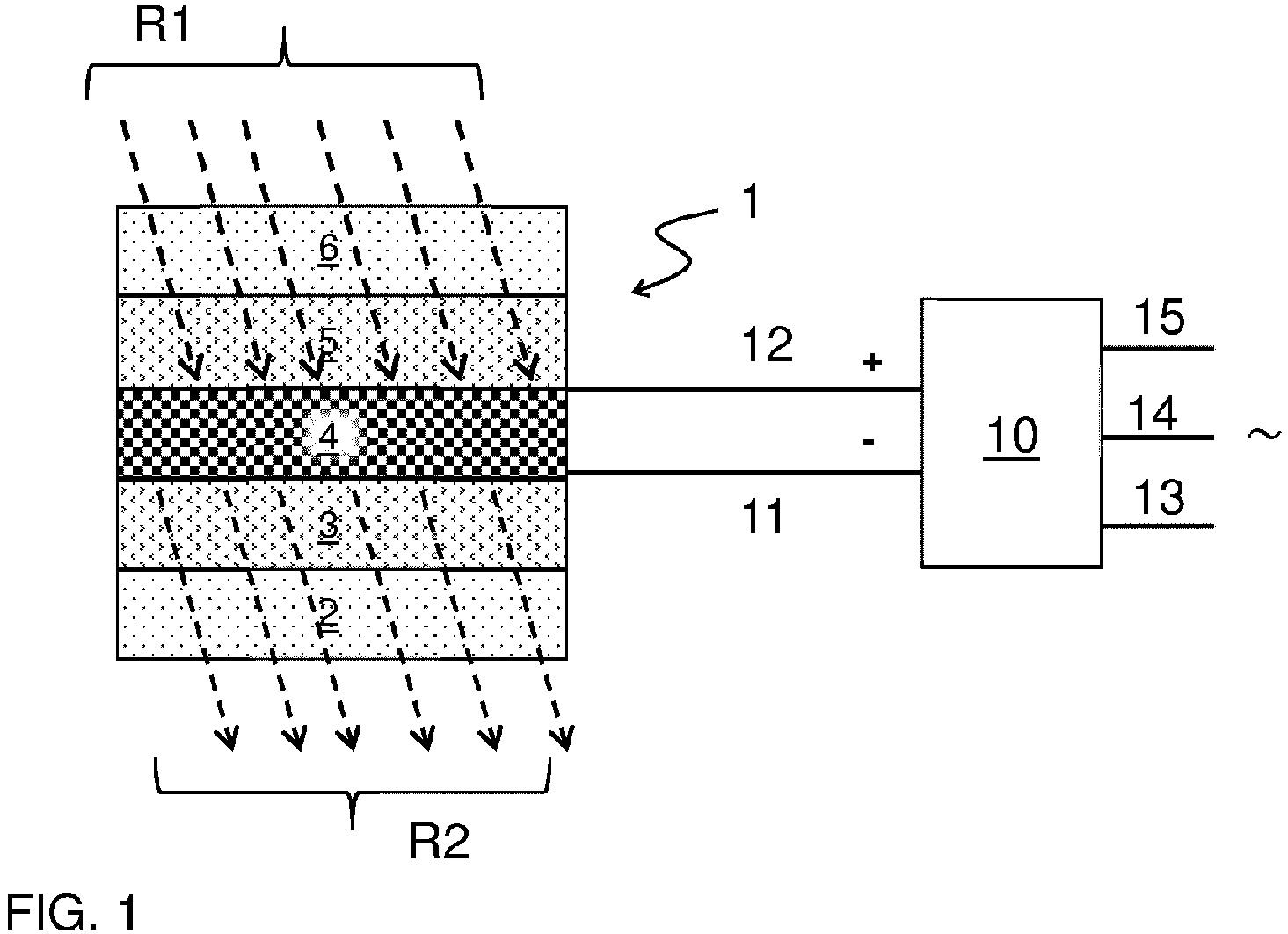
FIG. 1 schematically shows a partially translucentphotovoltaic window 1 that comprises aphotovoltaic module 4 enclosed between afirst window pane 2 and asecond window pane 6. As shown further inFIG. 1A , thephotovoltaic module 4 comprises a stack with at least a first electrode layer 41 (here a cathode), a second electrode layer 45 (anode) and a perovskitephotovoltaic layer 43 between said electrode layers. In the example shown, additionally anelectron transport layer 42 is provided between thefirst electrode layer 41 and thephotovoltaic layer 43. Also ahole transport layer 44 is provided between thesecond electrode layer 45 and thephotovoltaic layer 43. Thephotovoltaic window 1 further comprises a firstintermediate layer 3 between thefirst window pane 2 and thephotovoltaic module 4. Thephotovoltaic window 1 still further comprises a secondintermediate layer 5 between thesecond window pane 6 and thephotovoltaic module 4. The first and the secondintermediate layer - In the embodiment shown the first and the
second electrode layer photovoltaic module 4 are connected viaelectric conductors power converter 10 that is connected via a further set ofconductors power converter 10 via the further set ofconductors photovoltaic window 1 so as to serve as an attenuated illumination of an interior. To that end all parts of the partially translucentphotovoltaic window 1, except the perovskitephotovoltaic layer 43, are typically highly translucent. E.g. thewindow panes electron transport layer 42, thehole transport layer 44, as well as theintermediate layers photovoltaic layer 43. More preferably the translucency is at least 75% and still more preferably it is at least 90%. - The partially translucent
photovoltaic window 1 may be transparent, but in some applications that is not necessary or may not be desired. - It is noted that additional layers may be present, as sublayers of the above-mentioned layers, or as additional layers. For example, it may be contemplated to include a further electro-optical layer stack. Such a further electro-optical layer stack may for example serve to allow a user to electrically control a transparency of the partially translucent
photovoltaic window 1. This allows the user to change an appearance of thewindow 1 between transparent and opal, or in an intermediate state. In an other example an electro-optical layer stack may serve for conversion of electrical energy into light. Therewith thewindow 1 can serve as an active source of light in the absence of daylight. Also combinations of various electro-optical layer stacks may be provided. - By way of example the
window panes window panes window panes - Such resin materials may also be contemplated as a matrix for the
intermediate layers - Regarding the photo-
voltaic module 4, the perovskite materials therein typically have a crystal structure of ABX3, wherein A is an organic cation as methylammonium (CH3NH3)+, B is an inorganic cation, usually lead (II) (Pb2+), and X is a halogen atom such as iodine (I-), chlorine (Cl-), fluorine (F-) or bromine (Br-). Perovskite materials are particularly advantageous in that they can be processed relatively easily and in that their bandgap can be set to a desired value by a proper choice of the halide content. One of examples is methylammonium lead trihalide (CH3NH3PbX3), with an optical bandgap between 1.5 and 2.3 eV depending on halide content. Other more complex structures contain mixed A cations, such as Cesium (Cs+), methylammonium ((CH3NH3)+, MA), formamidinum ((H2NCHNH2)+, FA), or rubidium (Rb+) and mixed X anions. The examples of complex mixed perovskites are Cesium formamidinum lead trihalide CsxFA1-xPbIyBr3-y and Cesium Methylamonium formamidinum lead trihalide CsxMAzFA1-x-zPbIyBr3-y (where x<1, z<1, x+z<1). With the A-cations and X-anions ratio the bandgap and the physical properties of perovskite materials can be tuned. Other metals such as tin may replace the role of Pb in the B position of perovskite materials. An example thereof is CH3NH3SnI3. Also combinations of Sn with Pb perovskites having a wider bandgap in the range of 1.2 to 2.2 eV are possible. A perovskitephotovoltaic layer 43 may have a thickness in the range of 100 nm to 20 micron for example. - A translucent electrically conductive material for use in the first and the second electrode layers 41, 45 may be of an organic or an inorganic nature. Examples of organic translucent (transparent) electrically conductive materials are polyaniline, polythiophene, polypyrrole or doped polymers. Examples of inorganic translucent (transparent) electrically conductive materials are ITO (Indium Tin Oxide), IZO (Indium Zinc Oxide), ATO (Antimony Tin Oxide), or Tin Oxide can be used. Other metal oxides can work, including but not limited to Nickel-Tungsten-Oxide, Indium doped Zinc Oxide, Magnesium-Indium-Oxide. Also (combinations of) a thin metal layer, an oxide layer, or other e.g. a TCO or a metal oxide layer or a conducting polymer layer, such as PEDOT-PSS may be used.. For example a 7 nm layer of Silver may be sandwiched in between two 10 nm ITO layers. The transparent electrically conductive electrode layer may have a total thickness in the range of a few tens of nm to a few hundreds of nm, for example in a range between 100 and 200 nm, for example about 120 nm.
- As noted above, one or more charge carrier transport layers may be provided. For example a hole transport layer, here the charge
carrier transport layer 44, such as a nickel-oxide layer or a MoSe layer, may be provided between the anode (here layer 45) and thephotovoltaic layer 43. Further examples of hole transport materials for a hole transport layer have been summarized for example, in Kirk-Othmer Encyclopedia of Chemical Technology, Fourth Edition, Vol. 18, p. 837-860, 1996, by Y. Wang. Both hole transporting molecules and polymers can be used. In an embodiment a hole transport layer may have a thickness in the range of 10 to 200 nm. Additionally, an electron transport layer here thelayer 42 may be provided between the cathode (here 41) and thephotovoltaic layer 43. Suitable materials for this purpose are for example TiO2, SnO2, ZrO2 and ZnO: The electron transport layer may have a thickness in the range of a few nm to a few tens of nm. -
FIG. 2A shows an exceptional case wherein the window is damaged, for example due to a hailstone H incident onwindow pane 6. As shown inFIG. 2B , water W could penetrate trough the damaged portion of thewindow pane 6 into thephotovoltaic module 4. Solid state lead compound (in the form of perovskite crystals or potentially by products like PbI2 could then dissolve in the penetrated water to form Pb2+ ions. - As shown in
FIG. 2C , in the partially translucentphotovoltaic window 1 as provided herein, water having dissolved therein Pb2+ ions that migrates outward thephotovoltaic module 4 enters an intermediate layer, here the secondintermediate layer 5, wherein the dissolved lead ions react with the getter material and form an insoluble product, e.g. PbO. Therewith distribution of lead originating from the perovskitephotovoltaic layer 43 into the environment is mitigated also in case thewindow 1 is damaged. - By way of example, phosphor may be provided as the lead getter material. Dissolved lead ions or lead containing ions in contact therewith react to insoluble leadphosphate and are therewith immobilized. As another example Sulphur may be provided as the lead getter material. The latter immobilizes lead components as insoluble leadsulfides. Also combinations of lead getter materials may be used.
- In a first example, the dissolved Pb2+ ions react with a monohydrogen-phosphate to form an insoluble phosphate compound as follows.
5Pb2+ + 3HPO4 2- + X- → Pb5(PO4)3X (s) + 3H+
Therein the negative ion X- is for example one of OH-,F-,Cl-, so that the insoluble reaction product is leadhydroxyphosphate (Pb5(PO4)3OH), leadchlorophosphate (Pb5(PO4)3Cl) or leadfluorophosphate (Pb5(PO4)3Cl). - Instead of using the monohydrogen-phosphate ion in the getter material, alternatively the dihydrogen-phosphate ion may be used in the following reaction:
5Pb2+ + 3H2PO4 - + X- (X=OH,F,Cl) → Pb5(PO4)3X (s) + 6H+.
Likewise, the negative ion X- is for example one of OH-,F-,Cl-, so that the insoluble reaction product is leadhydroxyphosphate (Pb5(PO4)3OH), leadchlorophosphate (Pb5(PO4)3Cl) or leadfluorophosphate (Pb5(PO4)3Cl). - In a second example, the dissolved Pb2+ ions react with a sulphide ions S2- to form insoluble leadsulphide as follows.
Pb2+ + S2- → PbS.
- In the embodiment of the
photovoltaic window 1 shown inFIG. 1 theintermediate layers intermediate layers window 1 or in case a damage does occur, helps to maintain integrity of thewindow 1, so that removal of a damaged window is more easy. - In an example, the elastic polymer is an adhesive. One example thereof is Polyvinyl butyral (or PVB) .
-
FIG. 3A-3C schematically show a method of manufacturing a partially translucentphotovoltaic window 1 as a layered product. The method comprises a step S2 wherein afirst window pane 2 is provided. Thefirst window pane 2 here serves as a substrate on which subsequently a stack of layers is provided. In step S3 a firstintermediate layer 3 comprising a lead getter material is provided on thefirst window pane 2. Subsequently in step S4, layers of aphotovoltaic module 4 are provided. As shown in more detail inFIG. 3C , in this example step S4 comprises sub-steps S41-S45 as follows. - In the first sub-step S41 of step S4 a
first electrode layer 41, for example a cathode, is provided on the firstintermediate layer 3. - In the second sub-step S42 of step S4 a first charge
carrier transport layer 42, for example an electron transport layer is provided on thefirst electrode layer 41. - In the third sub-step S43 of step S4 a perovskite
photovoltaic layer 43, is provided on the first chargecarrier transport layer 42. - In the fourth sub-step S44 of step S4 a second charge
carrier transport layer 44, for example a hole transport layer is provided on the perovskitephotovoltaic layer 43. - In the fifth sub-step S45 of step S4 a
second electrode layer 45, for example an anode, is provided on the second chargecarrier transport layer 44. - Subsequently in step S5 a second
intermediate layer 5 comprising a lead getter material is provided on thephotovoltaic module 4. - Then, in a next step S6, the intermediate product so obtained is laminated with a
second window pane 6. - It is noted that various technologies are available for providing a layer in the steps referred to above. Various methods may be used for depositing and applying layers. Example of these methods may include spin-coating, printing methods, slot-die coating and vapor deposition methods like physical vapor deposition (e.g. E-beam PVD, Sputter PVD), (spatial) Atomic Layer Deposition ((s)ALD) and the like.
- Another exemplary method of manufacturing is depicted in
FIG. 4A, 4B . -
FIG. 4A shows a preparatory step S4 having sub-steps S41-S45 as shown inFIG. 3C , wherein aphotovoltaic module 4 is provided that comprises a stack with at least afirst electrode layer 41, asecond electrode layer 45 and a perovskitephotovoltaic layer 43 between said electrode layers. In preparatory sub-step S11, thefirst window pane 2 having the firstintermediate layer 3 is provided and in preparatory sub-step S12, thefirst window pane 6 having the secondintermediate layer 5 is provided. In subsequent step S13 the intermediary products obtain in preparatory steps S4, S11 and S12 are laminated into the partially translucentphotovoltaic window 1 shown inFIG. 4B . -
FIG. 5 schematically shows agreenhouse 20 provided with aroof 21 formed by partially translucentphotovoltaic windows 1 as shown inFIG. 1 , or being covered therewith. Thegreenhouse 20 shown inFIG. 3 encloses aninner space 22 for growingplants 23. In this embodiment, thephotovoltaic windows 1 comprised in theroof 21, or from which the roof is constructed has aphotovoltaic module 4, wherein the perovskitephotovoltaic layer 43 has a relative high absorption for radiation with a wavelength in the range of 500-600 nm, and has a relatively low absorption radiation for visible radiation outside this range. In particular it has a relatively low absorption for visible radiation in the subranges of 350-500 nm and 600-700 nm, Therewith the spectrum of the transmitted radiation R2 optimally matches the requirements for photosynthesis, as is illustrated by the sensitivity curves of chlorophyl-a and chlorophyl-b shown inFIG. 5A . -
FIG. 6 schematically shows ahouse 30 having aroof 31,front door 32,windows 33, 34 and further having an embodiment of partially translucentphotovoltaic window 1 as shown inFIG. 1 . Thephotovoltaic window 1 may be transparent, but may alternatively be opal, or may be controllably switched in either one of a transparent state or an opal state. The perovskite photovoltaic layer 43 (SeeFIG. 1A ) may have an absorption with a substantially uniform distribution over the visible spectrum, so that solar radiation R1 impingent on thewindow 1 is attenuated as R2, but gives the same color impression. Optionally the perovskitephotovoltaic layer 43 may have a relatively high absorption for radiation having a wavelength greater than 700 nm, to mitigate an undue heating of the interior of the house. - As used herein, the terms "comprises," "comprising," "includes," "including," "has," "having" or any other variation thereof, are intended to cover a non-exclusive inclusion. For example, a process, method, article, or apparatus that comprises a list of elements is not necessarily limited to only those elements but may include other elements not expressly listed or inherent to such process, method, article, or apparatus. Further, unless expressly stated to the contrary, "or" refers to an inclusive or and not to an exclusive or. For example, a condition A or B is satisfied by any one of the following: A is true (or present) and B is false (or not present), A is false (or not present) and B is true (or present), and both A and B are true (or present).
- Also, use of the "a" or "an" are employed to describe elements and components of the invention. This is done merely for convenience and to give a general sense of the invention. This description should be read to include one or at least one and the singular also includes the plural unless it is obvious that it is meant otherwise.
Claims (14)
- A partially translucent photovoltaic window (1), comprising a photovoltaic module (4) enclosed between a first window pane (2) and a second window pane (6), the photovoltaic module comprising a stack with at least a first electrode layer (41), a second electrode layer (45) and a perovskite photovoltaic layer (43) between said electrode layers, the photovoltaic window further comprising between said first window pane (2) and said photovoltaic module (4) and between said second window pane (6) and said photovoltaic module (4) a respective intermediate layer (3,5) comprising a lead getter material.
- The photovoltaic window according to claim 1, wherein at least one of said respective intermediate layers is of an elastic polymer, having said lead getter material dispersed therein.
- The photovoltaic window according to claim 2, wherein the elastic polymer is an adhesive.
- The photovoltaic window according to one of the previous claims, wherein the lead getter material comprises phosphor and or sulphur.
- The photovoltaic window according to one of the previous claims which is transparent.
- The photovoltaic window according to one of the previous claims, wherein the perovskite photovoltaic layer (43) has an absorption with a substantially uniform distribution over the visible spectrum.
- The photovoltaic window according to claim 6, wherein the perovskite photovoltaic layer (43) has a relatively high absorption for radiation having a wavelength greater than 700 nm.
- The photovoltaic window according to one of the previous claims, wherein the perovskite photovoltaic layer (43) has an absorption which is non-uniform over the visible spectrum.
- The photovoltaic window according to claim 8, wherein the perovskite photovoltaic layer (43) has a relative high absorption for radiation with a wavelength in the range of 500-600 nm, and has a relatively low absorption radiation for visible radiation outside this range, preferably has a relatively low absorption for visible radiation in the subranges of 350-500 nm and 600-700 nm,
- A method of manufacturing a partially translucent photovoltaic window (1) as a layered product, subsequently comprising:- a first window pane (2);- a first intermediate layer (3) comprising a lead getter material;- a photovoltaic module (4) comprising a stack with at least a first electrode layer (41), a second electrode layer (45) and a perovskite photovoltaic layer (43) between said electrode layers,- a second intermediate layer (5) comprising a lead getter material;- a second window pane (6).
- The method according to claim 10 comprising:- providing the first window pane (2) as a carrier;- depositing on the first window pane (2) at least the following sequence of layers;- said first intermediate layer (3);- said first electrode layer (41);- said perovskite photovoltaic layer (43);- said second electrode layer (45);- said second intermediate layer (5);- laminating the second window pane (6) on top of said sequence of layers deposited on the first window pane (2).
- The method according to claim 10 comprising:- providing a photovoltaic module (4) comprising a stack with at least a first electrode layer (41), a second electrode layer (45) and a perovskite photovoltaic layer (43) between said electrode layers;- providing the partially translucent photovoltaic window (1) by laminating the first window pane (2), the first intermediate layer (3), the photovoltaic module (4), the second intermediate layer (5) and the second window pane (6) into the layered product.
- A photovoltaic greenhouse (20) enclosing an inner space (22) for growing plants (23), and comprising a roof (21) formed of, or carrying, a partially translucent photovoltaic window (1) according to claim 9.
- A building, such as a house (30) comprising one or more partially translucent photovoltaic windows (1) according to claim 5, 6 or 7.
Priority Applications (5)
| Application Number | Priority Date | Filing Date | Title |
|---|---|---|---|
| EP20153934.3A EP3855509A1 (en) | 2020-01-27 | 2020-01-27 | Partially translucent photovoltaic window and method of manufacturing the same |
| US17/794,360 US12419189B2 (en) | 2020-01-27 | 2021-01-26 | Partially translucent photovoltaic window and method of manufacturing the same |
| EP21702323.3A EP4097767B1 (en) | 2020-01-27 | 2021-01-26 | Partially translucent photovoltaic window and method of manufacturing the same |
| CN202180011008.6A CN115004383A (en) | 2020-01-27 | 2021-01-26 | Partially translucent photovoltaic window and method of making same |
| PCT/NL2021/050045 WO2021154070A1 (en) | 2020-01-27 | 2021-01-26 | Partially translucent photovoltaic window and method of manufacturing the same |
Applications Claiming Priority (1)
| Application Number | Priority Date | Filing Date | Title |
|---|---|---|---|
| EP20153934.3A EP3855509A1 (en) | 2020-01-27 | 2020-01-27 | Partially translucent photovoltaic window and method of manufacturing the same |
Publications (1)
| Publication Number | Publication Date |
|---|---|
| EP3855509A1 true EP3855509A1 (en) | 2021-07-28 |
Family
ID=69326460
Family Applications (2)
| Application Number | Title | Priority Date | Filing Date |
|---|---|---|---|
| EP20153934.3A Withdrawn EP3855509A1 (en) | 2020-01-27 | 2020-01-27 | Partially translucent photovoltaic window and method of manufacturing the same |
| EP21702323.3A Active EP4097767B1 (en) | 2020-01-27 | 2021-01-26 | Partially translucent photovoltaic window and method of manufacturing the same |
Family Applications After (1)
| Application Number | Title | Priority Date | Filing Date |
|---|---|---|---|
| EP21702323.3A Active EP4097767B1 (en) | 2020-01-27 | 2021-01-26 | Partially translucent photovoltaic window and method of manufacturing the same |
Country Status (4)
| Country | Link |
|---|---|
| US (1) | US12419189B2 (en) |
| EP (2) | EP3855509A1 (en) |
| CN (1) | CN115004383A (en) |
| WO (1) | WO2021154070A1 (en) |
Cited By (2)
| Publication number | Priority date | Publication date | Assignee | Title |
|---|---|---|---|---|
| US20240047143A1 (en) * | 2020-12-21 | 2024-02-08 | Yissum Research Development Company Of The Hebrew University Of Jerusalem Ltd. | Solar energy and agroproduction structures and facilities |
| TWI902058B (en) * | 2023-11-15 | 2025-10-21 | 台灣鈣鈦礦科技股份有限公司 | Perovskite solar cell |
Families Citing this family (2)
| Publication number | Priority date | Publication date | Assignee | Title |
|---|---|---|---|---|
| WO2022113038A1 (en) * | 2020-11-30 | 2022-06-02 | King Abdullah University Of Science And Technology | Concurrent cationic and anionic metal halide perovskite defect passivation method and device |
| DE102024139948A1 (en) | 2024-06-10 | 2025-12-11 | Heliatek Gmbh | Optoelectronic component with a flame-retardant multilayer coating |
Citations (3)
| Publication number | Priority date | Publication date | Assignee | Title |
|---|---|---|---|---|
| US20130061542A1 (en) * | 2010-03-31 | 2013-03-14 | Pilkington Group Limited | Photovoltaic window assembly with solar control properties |
| US20140165460A1 (en) * | 2011-06-08 | 2014-06-19 | Nederlandse Organisatie Voor Toegepast-Natuurwe- Tenschappelijk Onderzoek Tno | Thin Film Solar Cell Module and Greenhouse Provided with the Same |
| WO2019145927A1 (en) * | 2018-01-29 | 2019-08-01 | Sunew Filmes Fotovoltaicos | Solar panel arrangement |
Family Cites Families (4)
| Publication number | Priority date | Publication date | Assignee | Title |
|---|---|---|---|---|
| JP2020504456A (en) * | 2017-01-10 | 2020-02-06 | ユビキタス エナジー, インコーポレイテッドUbiquitous Energy, Inc. | Window integrated transparent photovoltaic module |
| KR101811243B1 (en) * | 2017-01-13 | 2018-01-25 | 포항공과대학교 산학협력단 | NOVEL CODUCTIVE POLYMER FOR PREVENTING Pb ION LEAKAGE FROM PEROVSKITE SOLAR CELL AND SOLAR CELL COMPRISING THE SAME |
| WO2018157139A1 (en) * | 2017-02-27 | 2018-08-30 | Alliance For Sustainable Energy, Llc | Energy-harvesting chromogenic devices |
| US11174277B2 (en) * | 2019-05-29 | 2021-11-16 | Alliance For Sustainable Energy, Llc | Sequestering compositions and materials |
-
2020
- 2020-01-27 EP EP20153934.3A patent/EP3855509A1/en not_active Withdrawn
-
2021
- 2021-01-26 WO PCT/NL2021/050045 patent/WO2021154070A1/en not_active Ceased
- 2021-01-26 US US17/794,360 patent/US12419189B2/en active Active
- 2021-01-26 CN CN202180011008.6A patent/CN115004383A/en active Pending
- 2021-01-26 EP EP21702323.3A patent/EP4097767B1/en active Active
Patent Citations (3)
| Publication number | Priority date | Publication date | Assignee | Title |
|---|---|---|---|---|
| US20130061542A1 (en) * | 2010-03-31 | 2013-03-14 | Pilkington Group Limited | Photovoltaic window assembly with solar control properties |
| US20140165460A1 (en) * | 2011-06-08 | 2014-06-19 | Nederlandse Organisatie Voor Toegepast-Natuurwe- Tenschappelijk Onderzoek Tno | Thin Film Solar Cell Module and Greenhouse Provided with the Same |
| WO2019145927A1 (en) * | 2018-01-29 | 2019-08-01 | Sunew Filmes Fotovoltaicos | Solar panel arrangement |
Non-Patent Citations (5)
| Title |
|---|
| DS DLAMINI ET AL: "Comparative study of EVA-Cloisite<sup> </sup> 20A and heat-treated EVA-Cloisite<sup> </sup> 20A on heavy-metal adsorption properties", WATER SA, vol. 38, no. 4, 11 September 2012 (2012-09-11), XP055706912, DOI: 10.4314/wsa.v38i4.6 * |
| GILES E. EPERON ET AL: "Formamidinium lead trihalide: a broadly tunable perovskite for efficient planar heterojunction solar cells", ENERGY & ENVIRONMENTAL SCIENCE, vol. 7, no. 3, 1 January 2014 (2014-01-01), Cambridge, pages 982 - 988, XP055234624, ISSN: 1754-5692, DOI: 10.1039/c3ee43822h * |
| JIANG YAN ET AL: "Reduction of lead leakage from damaged lead halide perovskite solar modules using self-healing polymer-based encapsulation", NATURE ENERGY, NATURE PUBLISHING GROUP UK, LONDON, vol. 4, no. 7, 17 June 2019 (2019-06-17), pages 585 - 593, XP036833106, DOI: 10.1038/S41560-019-0406-2 * |
| SUN J ET AL: "Semi-transparent solar cells", JOURNAL OF PHYSICS D: APPLIED PHYSICS, INSTITUTE OF PHYSICS PUBLISHING LTD, GB, vol. 50, no. 9, 3 February 2017 (2017-02-03), pages 93001, XP020314253, ISSN: 0022-3727, [retrieved on 20170203], DOI: 10.1088/1361-6463/AA53D7 * |
| Y. WANG: "Kirk-Othmer Encyclopedia of Chemical Technology", vol. 18, 1996, pages: 837 - 860 |
Cited By (2)
| Publication number | Priority date | Publication date | Assignee | Title |
|---|---|---|---|---|
| US20240047143A1 (en) * | 2020-12-21 | 2024-02-08 | Yissum Research Development Company Of The Hebrew University Of Jerusalem Ltd. | Solar energy and agroproduction structures and facilities |
| TWI902058B (en) * | 2023-11-15 | 2025-10-21 | 台灣鈣鈦礦科技股份有限公司 | Perovskite solar cell |
Also Published As
| Publication number | Publication date |
|---|---|
| CN115004383A (en) | 2022-09-02 |
| EP4097767B1 (en) | 2026-04-29 |
| EP4097767A1 (en) | 2022-12-07 |
| US12419189B2 (en) | 2025-09-16 |
| WO2021154070A1 (en) | 2021-08-05 |
| US20230050607A1 (en) | 2023-02-16 |
Similar Documents
| Publication | Publication Date | Title |
|---|---|---|
| US12419189B2 (en) | Partially translucent photovoltaic window and method of manufacturing the same | |
| Chu et al. | Encapsulation: The path to commercialization of stable perovskite solar cells | |
| JP7048785B2 (en) | A transparent electrode, a manufacturing method thereof, and an electronic device using the transparent electrode. | |
| Ono et al. | Progress toward stable lead halide perovskite solar cells | |
| Mohammadi et al. | Encapsulation strategies for highly stable perovskite solar cells under severe stress testing: Damp heat, freezing, and outdoor illumination conditions | |
| US20170317305A1 (en) | Systems and methods for transparent organic photovoltaic devices | |
| CN103460434B (en) | Multi-layer part for the encapsulation of sensing element | |
| JP7092570B2 (en) | Solar cell module | |
| Castro-Hermosa et al. | Stability issues pertaining large area perovskite and dye-sensitized solar cells and modules | |
| EP3955328B1 (en) | Solar cell module | |
| Teixeira et al. | Selection of the ultimate perovskite solar cell materials and fabrication processes towards its industrialization: A review | |
| Pareja-Rivera et al. | Lead-free halide perovskites, beyond solar cells and LEDs | |
| EP2284903A1 (en) | Photovoltaic cell substrate and method of manufacturing the same | |
| EP4078684B1 (en) | Semi-translucent photovoltaic device and method of manufacturing the same | |
| JP4848666B2 (en) | Oxide semiconductor electrode transfer material, dye-sensitized solar cell substrate, dye-sensitized solar cell, and methods for producing the same | |
| KR20190143743A (en) | Solar cell and method of manufacturing the same | |
| US12396268B2 (en) | Photovoltaic device and method of manufacturing the same | |
| US20250204140A1 (en) | Adhesive bonding for bifacial and tandem solar cells | |
| US20200293135A1 (en) | Input device | |
| KR20190118379A (en) | Multilayer transparent electrodes and organic solar cells having the same | |
| KR20150048304A (en) | Solar cell including a transparent electrode having multilayer structure | |
| US20110203658A1 (en) | Photovoltaic cell substrate and photovoltaic cell including the same | |
| KR20170131995A (en) | Organic-inorgganic complex solar cell |
Legal Events
| Date | Code | Title | Description |
|---|---|---|---|
| PUAI | Public reference made under article 153(3) epc to a published international application that has entered the european phase |
Free format text: ORIGINAL CODE: 0009012 |
|
| STAA | Information on the status of an ep patent application or granted ep patent |
Free format text: STATUS: THE APPLICATION HAS BEEN PUBLISHED |
|
| AK | Designated contracting states |
Kind code of ref document: A1 Designated state(s): AL AT BE BG CH CY CZ DE DK EE ES FI FR GB GR HR HU IE IS IT LI LT LU LV MC MK MT NL NO PL PT RO RS SE SI SK SM TR |
|
| STAA | Information on the status of an ep patent application or granted ep patent |
Free format text: STATUS: THE APPLICATION IS DEEMED TO BE WITHDRAWN |
|
| 18D | Application deemed to be withdrawn |
Effective date: 20220129 |