EP3855497A1 - Solid-state imaging element and electronic device - Google Patents
Solid-state imaging element and electronic device Download PDFInfo
- Publication number
- EP3855497A1 EP3855497A1 EP19863094.9A EP19863094A EP3855497A1 EP 3855497 A1 EP3855497 A1 EP 3855497A1 EP 19863094 A EP19863094 A EP 19863094A EP 3855497 A1 EP3855497 A1 EP 3855497A1
- Authority
- EP
- European Patent Office
- Prior art keywords
- wiring
- solid
- state imaging
- imaging element
- element according
- Prior art date
- Legal status (The legal status is an assumption and is not a legal conclusion. Google has not performed a legal analysis and makes no representation as to the accuracy of the status listed.)
- Granted
Links
Images









Classifications
-
- H—ELECTRICITY
- H04—ELECTRIC COMMUNICATION TECHNIQUE
- H04N—PICTORIAL COMMUNICATION, e.g. TELEVISION
- H04N25/00—Circuitry of solid-state image sensors [SSIS]; Control thereof
- H04N25/70—SSIS architectures; Circuits associated therewith
- H04N25/76—Addressed sensors, e.g. MOS or CMOS sensors
- H04N25/77—Pixel circuitry, e.g. memories, A/D converters, pixel amplifiers, shared circuits or shared components
-
- H—ELECTRICITY
- H04—ELECTRIC COMMUNICATION TECHNIQUE
- H04N—PICTORIAL COMMUNICATION, e.g. TELEVISION
- H04N25/00—Circuitry of solid-state image sensors [SSIS]; Control thereof
- H04N25/50—Control of the SSIS exposure
- H04N25/53—Control of the integration time
- H04N25/532—Control of the integration time by controlling global shutters in CMOS SSIS
-
- H—ELECTRICITY
- H04—ELECTRIC COMMUNICATION TECHNIQUE
- H04N—PICTORIAL COMMUNICATION, e.g. TELEVISION
- H04N25/00—Circuitry of solid-state image sensors [SSIS]; Control thereof
- H04N25/60—Noise processing, e.g. detecting, correcting, reducing or removing noise
- H04N25/616—Noise processing, e.g. detecting, correcting, reducing or removing noise involving a correlated sampling function, e.g. correlated double sampling [CDS] or triple sampling
-
- H—ELECTRICITY
- H04—ELECTRIC COMMUNICATION TECHNIQUE
- H04N—PICTORIAL COMMUNICATION, e.g. TELEVISION
- H04N25/00—Circuitry of solid-state image sensors [SSIS]; Control thereof
- H04N25/60—Noise processing, e.g. detecting, correcting, reducing or removing noise
- H04N25/62—Detection or reduction of noise due to excess charges produced by the exposure, e.g. smear, blooming, ghost image, crosstalk or leakage between pixels
-
- H—ELECTRICITY
- H04—ELECTRIC COMMUNICATION TECHNIQUE
- H04N—PICTORIAL COMMUNICATION, e.g. TELEVISION
- H04N25/00—Circuitry of solid-state image sensors [SSIS]; Control thereof
- H04N25/60—Noise processing, e.g. detecting, correcting, reducing or removing noise
- H04N25/65—Noise processing, e.g. detecting, correcting, reducing or removing noise applied to reset noise, e.g. KTC noise related to CMOS structures by techniques other than CDS
-
- H—ELECTRICITY
- H04—ELECTRIC COMMUNICATION TECHNIQUE
- H04N—PICTORIAL COMMUNICATION, e.g. TELEVISION
- H04N25/00—Circuitry of solid-state image sensors [SSIS]; Control thereof
- H04N25/70—SSIS architectures; Circuits associated therewith
- H04N25/76—Addressed sensors, e.g. MOS or CMOS sensors
- H04N25/766—Addressed sensors, e.g. MOS or CMOS sensors comprising control or output lines used for a plurality of functions, e.g. for pixel output, driving, reset or power
-
- H—ELECTRICITY
- H04—ELECTRIC COMMUNICATION TECHNIQUE
- H04N—PICTORIAL COMMUNICATION, e.g. TELEVISION
- H04N25/00—Circuitry of solid-state image sensors [SSIS]; Control thereof
- H04N25/70—SSIS architectures; Circuits associated therewith
- H04N25/76—Addressed sensors, e.g. MOS or CMOS sensors
- H04N25/77—Pixel circuitry, e.g. memories, A/D converters, pixel amplifiers, shared circuits or shared components
- H04N25/771—Pixel circuitry, e.g. memories, A/D converters, pixel amplifiers, shared circuits or shared components comprising storage means other than floating diffusion
-
- H—ELECTRICITY
- H10—SEMICONDUCTOR DEVICES; ELECTRIC SOLID-STATE DEVICES NOT OTHERWISE PROVIDED FOR
- H10F—INORGANIC SEMICONDUCTOR DEVICES SENSITIVE TO INFRARED RADIATION, LIGHT, ELECTROMAGNETIC RADIATION OF SHORTER WAVELENGTH OR CORPUSCULAR RADIATION
- H10F39/00—Integrated devices, or assemblies of multiple devices, comprising at least one element covered by group H10F30/00, e.g. radiation detectors comprising photodiode arrays
- H10F39/10—Integrated devices
- H10F39/12—Image sensors
- H10F39/15—Charge-coupled device [CCD] image sensors
- H10F39/153—Two-dimensional or three-dimensional array CCD image sensors
-
- H—ELECTRICITY
- H10—SEMICONDUCTOR DEVICES; ELECTRIC SOLID-STATE DEVICES NOT OTHERWISE PROVIDED FOR
- H10F—INORGANIC SEMICONDUCTOR DEVICES SENSITIVE TO INFRARED RADIATION, LIGHT, ELECTROMAGNETIC RADIATION OF SHORTER WAVELENGTH OR CORPUSCULAR RADIATION
- H10F39/00—Integrated devices, or assemblies of multiple devices, comprising at least one element covered by group H10F30/00, e.g. radiation detectors comprising photodiode arrays
- H10F39/10—Integrated devices
- H10F39/12—Image sensors
- H10F39/18—Complementary metal-oxide-semiconductor [CMOS] image sensors; Photodiode array image sensors
-
- H—ELECTRICITY
- H10—SEMICONDUCTOR DEVICES; ELECTRIC SOLID-STATE DEVICES NOT OTHERWISE PROVIDED FOR
- H10F—INORGANIC SEMICONDUCTOR DEVICES SENSITIVE TO INFRARED RADIATION, LIGHT, ELECTROMAGNETIC RADIATION OF SHORTER WAVELENGTH OR CORPUSCULAR RADIATION
- H10F39/00—Integrated devices, or assemblies of multiple devices, comprising at least one element covered by group H10F30/00, e.g. radiation detectors comprising photodiode arrays
- H10F39/80—Constructional details of image sensors
- H10F39/803—Pixels having integrated switching, control, storage or amplification elements
-
- H—ELECTRICITY
- H10—SEMICONDUCTOR DEVICES; ELECTRIC SOLID-STATE DEVICES NOT OTHERWISE PROVIDED FOR
- H10F—INORGANIC SEMICONDUCTOR DEVICES SENSITIVE TO INFRARED RADIATION, LIGHT, ELECTROMAGNETIC RADIATION OF SHORTER WAVELENGTH OR CORPUSCULAR RADIATION
- H10F39/00—Integrated devices, or assemblies of multiple devices, comprising at least one element covered by group H10F30/00, e.g. radiation detectors comprising photodiode arrays
- H10F39/80—Constructional details of image sensors
- H10F39/803—Pixels having integrated switching, control, storage or amplification elements
- H10F39/8037—Pixels having integrated switching, control, storage or amplification elements the integrated elements comprising a transistor
-
- H—ELECTRICITY
- H10—SEMICONDUCTOR DEVICES; ELECTRIC SOLID-STATE DEVICES NOT OTHERWISE PROVIDED FOR
- H10F—INORGANIC SEMICONDUCTOR DEVICES SENSITIVE TO INFRARED RADIATION, LIGHT, ELECTROMAGNETIC RADIATION OF SHORTER WAVELENGTH OR CORPUSCULAR RADIATION
- H10F39/00—Integrated devices, or assemblies of multiple devices, comprising at least one element covered by group H10F30/00, e.g. radiation detectors comprising photodiode arrays
- H10F39/80—Constructional details of image sensors
- H10F39/805—Coatings
-
- H—ELECTRICITY
- H10—SEMICONDUCTOR DEVICES; ELECTRIC SOLID-STATE DEVICES NOT OTHERWISE PROVIDED FOR
- H10F—INORGANIC SEMICONDUCTOR DEVICES SENSITIVE TO INFRARED RADIATION, LIGHT, ELECTROMAGNETIC RADIATION OF SHORTER WAVELENGTH OR CORPUSCULAR RADIATION
- H10F39/00—Integrated devices, or assemblies of multiple devices, comprising at least one element covered by group H10F30/00, e.g. radiation detectors comprising photodiode arrays
- H10F39/80—Constructional details of image sensors
- H10F39/811—Interconnections
-
- H—ELECTRICITY
- H10—SEMICONDUCTOR DEVICES; ELECTRIC SOLID-STATE DEVICES NOT OTHERWISE PROVIDED FOR
- H10F—INORGANIC SEMICONDUCTOR DEVICES SENSITIVE TO INFRARED RADIATION, LIGHT, ELECTROMAGNETIC RADIATION OF SHORTER WAVELENGTH OR CORPUSCULAR RADIATION
- H10F39/00—Integrated devices, or assemblies of multiple devices, comprising at least one element covered by group H10F30/00, e.g. radiation detectors comprising photodiode arrays
- H10F39/80—Constructional details of image sensors
- H10F39/812—Arrangements for transferring the charges in the image sensor perpendicular to the imaging plane, e.g. buried regions used to transfer generated charges to circuitry under the photosensitive region
-
- H—ELECTRICITY
- H10—SEMICONDUCTOR DEVICES; ELECTRIC SOLID-STATE DEVICES NOT OTHERWISE PROVIDED FOR
- H10F—INORGANIC SEMICONDUCTOR DEVICES SENSITIVE TO INFRARED RADIATION, LIGHT, ELECTROMAGNETIC RADIATION OF SHORTER WAVELENGTH OR CORPUSCULAR RADIATION
- H10F39/00—Integrated devices, or assemblies of multiple devices, comprising at least one element covered by group H10F30/00, e.g. radiation detectors comprising photodiode arrays
- H10F39/80—Constructional details of image sensors
- H10F39/802—Geometry or disposition of elements in pixels, e.g. address-lines or gate electrodes
Definitions
- the present disclosure relates to a solid-state imaging element and an electronic device, and more particularly to a solid-state imaging element and an electronic device capable of increasing the capacitance of a charge holding unit.
- an image sensor that performs global shutter type imaging in which all pixels simultaneously transfer charges from a photodiode (PD) to a floating diffusion (FD).
- PD photodiode
- FD floating diffusion
- kTC noise is generated at reset when driving an image sensor.
- Patent Document 1 discloses an image sensor that performs a global shutter type imaging including a charge holding unit different from the FD and feeding a signal potential including the kTC noise back to the FD to reduce the kTC noise.
- Patent Document 1 Japanese Patent Application Laid-Open No. 2018-64199
- Patent Document 1 since the kTC noise is reduced by the capacitance distribution of the coupling capacitance between the charge holding unit and the FD, it is necessary to increase the capacitance of the charge holding unit, but Patent Document 1 does not disclose any specific configuration for increasing the capacitance of the charge holding unit.
- the present disclosure has been made in view of such a situation, and is intended to increase the capacitance of the charge holding unit.
- the solid-state imaging element of the present disclosure is a solid-state imaging element including: a pixel including a photodiode, an FD that accumulates charges generated in the photodiode, and a charge holding unit that is connected in parallel with the FD, in which the charge holding unit includes a wiring capacitance formed by parallel running of a first wiring connected to a first potential and a second wiring connected to a second potential different from the first potential.
- the electronic device of the present disclosure is an electronic device including: a solid-state imaging element including a pixel including a photodiode, an FD that accumulates charges generated in the photodiode, and a charge holding unit that is connected in parallel with the FD, in which the charge holding unit includes a wiring capacitance formed by parallel running of a first wiring connected to a first potential and a second wiring connected to a second potential different from the first potential.
- a pixel includes a photodiode, an FD that accumulates charges generated in the photodiode, and a charge holding unit that is connected in parallel with the FD, in which the charge holding unit includes a wiring capacitance formed by parallel running of a first wiring connected to a first potential and a second wiring connected to a second potential different from the first potential.
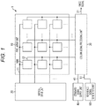
- Fig. 1 is a diagram showing a configuration example of a solid-state imaging element 1 to which the technology according to the present disclosure is applied.
- the solid-state imaging element 1 includes a pixel array unit 10, a vertical drive unit 20, a column signal processing unit 30, a standard signal supply unit 40, and a reference signal generation unit 50.
- the pixel array unit 10 generates an image signal according to incident light.
- the pixel array unit 10 includes pixels 100 having a photoelectric conversion unit in a two-dimensional matrix.
- a control line 11 for transmitting a control signal to the pixel 100 and a vertical signal line 12 for transmitting an image signal generated by the pixel 100 are wired in an X-Y matrix.
- the control line 11 is wired for each row of a plurality of pixels 100.
- the control line 11 is commonly wired to the pixels 100 arranged in one row. That is, control signals different with respect to each row are input to the pixels 100, and a common control signal is input to the pixels 100 arranged in one row.
- the vertical signal line 12 is wired for each column of the plurality of pixels 100.
- the vertical signal line 12 is commonly wired to the pixels 100 arranged in one column. That is, an image signal of the pixels 100 arranged in one column is transmitted via the common vertical signal line 12.
- the vertical drive unit 20 generates a control signal and outputs it to the pixel array unit 10 via the control line 11.
- the column signal processing unit 30 processes the image signal output from the pixel array unit 10.
- the image signal processed by the column signal processing unit 30 corresponds to an output signal of the solid-state imaging element 1, and is output to the outside of the solid-state imaging element 1.
- the standard signal supply unit 40 generates a standard signal.
- the standard signal is a signal that serves as a standard of the image signal generated by the pixel 100, and is, for example, a signal having a voltage corresponding to a black level image signal.
- the generated standard signal is supplied to the column signal processing unit 30 via a standard signal line 41.
- the reference signal generation unit 50 generates a reference signal.
- the reference signal is a signal serving as a standard for analog-to-digital conversion of the image signal generated by the pixel 100.
- As the reference signal for example, a signal whose voltage drops like a lamp can be adopted.
- the generated reference signal is output to the column signal processing unit 30 via a reference signal line 51.
- Fig. 2 is a diagram showing a configuration example of the pixel 100 to which the technology described above according to the present disclosure is applied.
- the pixel 100 includes a photodiode (PD) 101, a transfer transistor 102, a floating diffusion (FD) 103, a reset transistor 104, an amplification transistor 105, and a selection transistor 106.
- a MOS transistor can be used for each pixel transistor: the transfer transistor 102, the reset transistor 104, the amplification transistor 105, and the selection transistor 106.
- control line 11 and the vertical signal line 12 described above are wired to the pixel 100.
- the control line 11 includes a control line transfer gate (TRG), a control line reset (RST), and a control line select (SEL). These control lines are connected to the gate of the MOS transistor and transmit the control signal described in Fig. 1 . When a voltage equal to or higher than a threshold voltage between the gate and the source of the MOS transistor is input to these control lines, the corresponding MOS transistor becomes conductive.
- the control line TRG transmits a signal for controlling on/off of the transfer transistor 102.
- the control line RST transmits a signal for controlling the reset of the FD 103.
- the control line SEL transmits a signal for selecting the pixel 100.
- a power line Vdd is wired to the pixel 100.
- the power line Vdd supplies power with positive polarity.
- the anode of the PD 101 is grounded and the cathode is connected to the source of the transfer transistor 102.
- the gate of the transfer transistor 102 is connected to the control line TRG, and the drain is connected to one end of the FD 103, the gate of the amplification transistor 105, and the source of the reset transistor 104. Another end of the FD 103 is grounded.
- the drain of the reset transistor 104 is connected to the power line Vdd and the gate is connected to the control line RST.
- the drain of the amplification transistor 105 is connected to the power line Vdd and the source is connected to the drain of the selection transistor 106.
- the gate of the selection transistor 106 is connected to the control line SEL and the source is connected to the vertical signal line 12.
- the PD 101 generates a charge according to the emitted incident light by photoelectric conversion.
- the transfer transistor 102 transfers the charge generated by the PD 101 to the FD 103.
- the transfer transistor 102 transfers the charge by causing the PD 101 and the FD 103 to be conductive.
- the FD 103 accumulates the charge generated in the PD 101.
- the FD 103 is formed in a diffusion layer of a semiconductor substrate such as a Si substrate and the like.
- the reset transistor 104 resets the charge accumulated in the FD 103.
- the reset transistor 104 applies a power voltage to the FD 103 by conducting the power line Vdd and the FD 103, and resets the FD 103.
- the amplification transistor 105 detects a signal corresponding to the charge held in the FD 103 as a pixel signal.
- the selection transistor 106 outputs the image signal detected by the amplification transistor 105.
- the selection transistor 106 outputs an image signal by causing the amplification transistor 105 and the vertical signal line 12 to be conductive.
- the solid-state imaging element 1 can perform global shutter type imaging.
- the pixel 100 further includes charge holding units 107, 108.
- the charge holding units 107, 108 are electrically connected in parallel with the FD 103 and accumulate charges generated in the PD 101 apart from the FD 103.
- One end of the charge holding unit 107 is connected to the drain of the transfer transistor 102, the gate of the amplification transistor 105, and the source of the reset transistor 104, and another end is connected to a node A having a predetermined potential. Furthermore, one end of the charge holding unit 108 is connected to the node A, and another end is grounded.
- the charge holding units 107, 108 can be formed by the wiring capacitance.
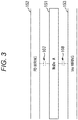
- Fig. 3 is a plan view showing an example of a wiring layout for forming the charge holding units 107, 108.
- Fig. 3 shows the layout of a part of each of a wiring 151 connected to the node A, a FD wiring 152 connecting the drain of the transfer transistor 102 and the gate of the amplification transistor 105, and a fixed potential line 153 connected to the fixed potential Vss different from the node A.
- the fixed potential Vss is assumed to be a ground potential (GND).
- the wiring 151, the FD wiring 152, and the fixed potential line 153 are laid out side by side so as to extend in the same direction (right-and-left direction in the drawing).
- the fact that wirings X, Y are laid out side by side means that the wirings X, Y run in parallel.
- the wiring 151 and the FD wiring 152 run in parallel to form the charge holding unit 107, and the wiring 151 and the fixed potential line 153 run in parallel to form the charge holding unit 108.
- the wiring 151, the FD wiring 152, and the fixed potential line 153 have only a straight portion extending in one direction (hereinafter referred to as an extending portion), but may have a portion bending or branching in a predetermined direction (hereinafter referred to as a bent portion).
- the bent portion can be formed in any of an L-shape, a T-shape, a U-shape, and a cross shape.
- the two wirings may run in parallel, for example, such that the bent portion of each of the two wirings is bent in the same direction or the bent portion of another wiring is bent so as to surround at least a part of one wiring.
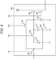
- Fig. 4 is a diagram showing a configuration example of a pixel 100 according to the first embodiment of the present disclosure.
- the pixel 100 of Fig. 4 differs from the pixel 100 of Fig. 2 in that it includes a feedback transistor 201.
- a MOS transistor can be used as the feedback transistor 201.
- a control line feedback is further wired as a control line 11 to the pixel 100 of Fig. 4 .
- the control line FB transmits a signal for controlling the supply of a reset voltage.
- the reset voltage is a voltage input to the pixel 100 when the pixel 100 is reset.
- the source of the feedback transistor 201 is connected to the drain of the reset transistor 104 and the node 202 at a predetermined potential.
- the drain of the feedback transistor 201 is connected to the column signal processing unit 30, and the gate is connected to the control line FB.
- a node 202 corresponds to the node A of the pixel 100 of Fig. 2 . Furthermore, in the pixel 100 of Fig. 4 , charge holding units 211, 212 corresponding to the charge holding units 107, 108 of the pixel 100 of Fig. 2 are formed.
- the feedback transistor 201 causes the charge holding unit 212 to hold the reset voltage output from the column signal processing unit 30.
- the charge holding unit 212 holds the reset voltage output from the feedback transistor 201.
- the reset transistor 104 applies a reset voltage to the FD 103 by conducting the charge holding unit 212 and the FD 103, and resets the FD 103.
- the charge holding unit 211 transmits the reset voltage held by the charge holding unit 212 to the FD 103.
- the kTC noise remains in the FD 103 at the time of reset.
- the kTC noise is noise caused by the operation of the reset transistor 104, and is generated when the reset transistor 104 shifts from the conductive state to the nonconductive state. Then, a part of it remains in the FD 103. It is known that the kTC noise can be reduced by reducing the electrostatic capacitance of the FD 103.
- the charge holding units 211, 212 are connected in parallel with the FD 103, and the capacitance of the FD 103 is distributed to the charge holding units 211, 212. Therefore, the kTC noise can be reduced.
- the capacitance of the charge holding units 211, 212 is increased by the wiring layout.
- Figs. 5 to 8 are plan views showing an example of the wiring layout of the wiring layers of the first layer to the fourth layer corresponding to the pixel 100 of Fig. 4 .
- Fig. 5 shows the wiring layout of a wiring layer M1 of the first layer directly above the Si substrate on which the PD 101 and each pixel transistor are formed.
- the PD 101 is arranged substantially in the center of the Si substrate shown in Fig. 5 , and the transfer transistor 102 is formed in the upper left part thereof.
- the amplification transistor 105 and the selection transistor 106 are formed side by side above the transfer transistor 102 in the drawing.
- the reset transistor 104 and the feedback transistor 201 are formed side by side on the upper right side of the PD 101 in the drawing.
- the reset transistor 104 and the feedback transistor 201 are pixel transistors constituting a pixel 100 corresponding to a PD 101, which is not shown, which is adjacent to the right side of the PD 101 shown in Fig. 5 . Therefore, a reset transistor 104 and a feedback transistor 201 constituting the pixel 100 corresponding to the PD 101 shown in Fig. 5 are formed on the left side of the PD 101, which is not shown.
- the wiring pattern of the wiring layer M1 is shown as a diagonal grid pattern.
- a FD wiring 251-1 connecting the transfer transistor 102 and the amplification transistor 105 is formed in the wiring layer M1.
- a large area pattern 252 for improving the sensitivity of the PD 101 by reflection of incident light is formed in the wiring layer M1.
- a control line 253-1 for supplying a control signal to the gate of the transfer transistor 102 is formed.
- the control line 253-1 is formed so that the extending portion and the bent portion, which are a part of the control line 253-1, run in parallel with the FD wiring 251-1.
- a wiring 202-1 for transmitting the potential of the node 202 to the wiring layer above the second layer is formed.
- Fig. 6 shows the wiring layout of the wiring layer M2 of the second layer.
- the wiring pattern of the wiring layer M2 is shown as a dot pattern.
- a wiring 202-2 that is electrically connected to the wiring 202-1 through a via is formed from the position corresponding to the wiring 202-1 of the wiring layer M1.
- the wiring 202-2 is generally formed in an L shape.
- a fixed potential line 271-2a connected to a fixed potential Vss (GND) is formed above the wiring 202-2 in the drawing.
- the fixed potential line 271-2a is formed by combining an extending portion and a plurality of L-shaped, T-shaped, and U-shaped bent portions along the upper side of the wiring 202-2 in the drawing.
- the fixed potential line 271-2a is formed so that the extending portion and the bent portion, which are a part of the fixed potential line 271-2a, run in parallel with the wiring 202-2. Therefore, the wiring capacitance is formed between the wiring 202-2 connected to the node 202 and the fixed potential line 271-2a connected to GND.
- an FD wiring 251-2 electrically connected to the FD wiring 251-1 of the wiring layer M1 through a via is formed below the wiring 202-2 in the drawing.
- the FD wiring 251-2 is formed by combining an extending portion and a plurality of L-shaped, T-shaped, and U-shaped bent portions.
- the FD wiring 251-2 is formed so that the extending portion, which is a part of the FD wiring 251-2, runs in parallel with the wiring 202-2. Therefore, the wiring capacitance (coupling capacitance with the FD 103) is formed between the wiring 202-2 connected to the node 202 and the FD wiring 251-2 connected to the FD 103. Note that, in the example of Fig. 6 , the wiring 202-2 and the FD wiring 251-2 are wirings corresponding to a pixel 100, which is not shown, adjacent to the right side of the pixel 100 shown in Fig. 6 .
- a fixed potential line 271-2b connected to the fixed potential Vss is formed below the FD wiring 251-2 in the drawing.
- the fixed potential line 271-2b is formed by combining an extending portion and a plurality of L-shaped and U-shaped bent portions along the left side, the upper side, and the right side of the FD wiring 251-2 in the drawing.
- control line 253-2 that is electrically connected to the control line 253-1 of the wiring layer M1 through a via is formed.
- the control line 253-2 is generally formed in an L shape.
- the FD wiring 251-2 is formed so that the extending portion and the bent portion, which are a part of the FD wiring 251-2, run in parallel with the fixed potential line 271-2b and the control line 253-2. Therefore, a wiring capacitance is also formed between the FD wiring 251-2 connected to the FD 103 and the fixed potential line 271-2b and the control line 253-2.
- the wiring 202-2 and the FD wiring 251-2 which are the signal lines connected to the FD 103 and the charge holding units 211, 212 that accumulate charges, which become pixel signals, are preferably surrounded by the fixed potential lines 271-2a, 271-2b and the control line 253-2 so as to be shielded from signal lines of adjacent pixels.
- Fig. 7 shows the wiring layout of the wiring layer M3 of the third layer.
- the wiring pattern of the wiring layer M3 is shown as an upward-sloping diagonal pattern. As shown in Fig. 7 , the wiring pattern of the wiring layer M3 is mainly formed so as to extend in the right-and-left direction in the drawing.
- a wiring 202-3a that is electrically connected to the wiring 202-2 of the wiring layer M2 through a via is formed at the position corresponding to the substantially left half of the PD 101.
- the wiring 202-3a is formed by combining an extending portion and a plurality of T-shaped and cross-shaped bent portions.
- a wiring 202-3b that is electrically connected to the wiring 202-2 of the wiring layer M2 through a via is formed at the position corresponding to the substantially right half of the PD 101.
- the wiring 202-3b is formed by combining an extending portion and a plurality of L-shaped, T-shaped, and U-shaped bent portions.
- a fixed potential line 271-3 connected to the fixed potential Vss is formed.
- the fixed potential line 271-3 is formed by combining an extending portion and a plurality of L-shaped, T-shaped, and cross-shaped bent portions so as to surround each of the four sides of the wiring 202-3a, 202-3b.
- the wirings 202-3a, 202-3b and the fixed potential line 271-3 are formed in a comb shape in which a part thereof faces each other.
- control line 253-3 that is electrically connected to the control line 253-2 of the wiring layer M2 through a via is formed.
- the control line 253-3 is formed in a straight line extending in the right-and-left direction in the drawing.
- the fixed potential line 271-3 is formed so that the extending portion and the bent portion, which are a part of the fixed potential line 271-3, run in parallel with the wirings 202-3a, 202-3b. Therefore, the wiring capacitance is formed between the wirings 202-3a, 202-3b connected to the node 202 and the fixed potential line 271-3 connected to GND.
- the wirings 202-3a, 202-3b which are the signal lines connected to the charge holding units 211, 212 that accumulate charges, which become pixel signals, are preferably surrounded by the fixed potential line 271-3 and the control line 253-3 so as to be shielded from signal lines of adjacent pixels.
- Fig. 8 shows the wiring layout of the wiring layer M4 of the fourth layer.
- the wiring pattern of the wiring layer M4 is shown as a grid pattern.
- fixed potential lines 271-4 connected to the fixed potential Vss are formed as a plurality of shielded wirings.
- a plurality of shielded fixed potential lines 271-4 is formed side by side in the right-and-left direction so as to extend in a straight line in the up-and-down direction in the drawing. Therefore, crosstalk between the signal lines connected to the FD 103 and the charge holding units 211, 212 that accumulate charges, which become pixel signals, is suppressed.
- the pixel 100 includes the configuration in which a wiring capacitance is formed by wirings running in parallel in the same wiring layer, and also includes the configuration in which a wiring capacitance is formed between different wiring layers.
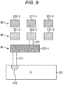
- Fig. 9 is a diagram showing an example of a cross section of a wiring layer of the pixel 100.
- Fig. 9 shows cross sections of a Si substrate 301 and wirings in the wiring layers M1 to M3.
- an N-type diffusion layer 310 serving as the node 202 is formed within a large P-type diffusion layer formed.
- the diffusion layer 310 formed on the Si substrate 301 and the wiring 202-1 of the wiring layer M1 are connected by a contact 311. Furthermore, the wiring 202-1 of the wiring layer M1 and the wiring 202-2 of the wiring layer M2 are connected by a via 312.
- the wiring 202-2 having a predetermined potential, the fixed potential line 271-2, and the FD wiring 251-2 run in parallel. Furthermore, within the wiring layer M3, the wiring 202-3 having a predetermined potential and the fixed potential line 271-3 run in parallel.
- the wiring 202-2 having a predetermined potential and the fixed potential line 271-3 run in parallel, and the fixed potential line 271-2 and the wiring 202-3 having a predetermined potential run in parallel.
- the wiring capacitance is formed by running the wirings in parallel not only within the same wiring layer but also between different wiring layers.
- the high capacitance of the charge holding unit connected in parallel with the FD can be realized by the wiring capacitance formed by the wiring connected to the node having a predetermined voltage, the fixed potential line, and the FD wiring running in parallel, and eventually the kTC noise can be reduced.
- the wiring patterns of the wiring layers M1 to M4 described above are formed in the same wiring layout for all the pixels 100. Therefore, the sensitivity non-uniformity between the pixels 100 can be reduced.
- a read circuit In a solid-state imaging element that performs global shutter type imaging, a read circuit cannot be shared between pixels. Therefore, it has been necessary to reduce the voltage amplitude of the pixel signal so that the pixel signal can be received in the subsequent circuit. For that purpose, it has been necessary to intentionally lower the conversion efficiency by increasing the capacitance of the FD.
- the large area pattern 252 for improving the sensitivity of PD by the reflection of incident light is formed directly above the PD.
- wirings running in parallel are formed directly above the PD.
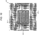
- Fig. 10 is a plan view showing another example of the wiring layout of the wiring layer M1 of the first layer corresponding to the pixel 100.
- the wiring 202-1 having a predetermined potential, the FD wiring 251-1, and the fixed potential line 271-1 are formed directly above the PD 101.
- the wiring 202-1 having a comb shape and a part of the FD wiring 251-1 having an L-shape are formed to run in parallel, and the fixed potential line 271-1 having a comb shape is formed to surround the wiring 202-1 and the FD wiring 251-1.
- the wiring 202-1 and the fixed potential line 271-1 are formed so that the comb-shaped portions face each other.
- the wiring 202-1, the FD wiring 251-1, and the fixed potential line 271-1 directly above the PD 101 are formed so that the L/S (line width of the pattern and the distance between the patterns) becomes narrower than the wavelength to be captured.
- the wiring pattern of the wiring layer M1 is formed in the same wiring layout for all the pixels 100. Therefore, the sensitivity non-uniformity between the pixels 100 can be reduced.
- Fig. 11 is a diagram showing another example of the cross section of the wiring layer of the pixel 100.
- a high-k film 331 having a high dielectric constant is provided as an insulating film between the wirings forming the wiring capacitance in the wiring layers M2, M3.
- Fig. 12 is a diagram showing still another example of the cross section of the wiring layer of the pixel 100.
- a diffusion layer 310' is formed on the Si substrate 301 instead of the diffusion layer 310.
- the diffusion layer 310' is formed to have a larger area than the diffusion layer 351 forming the pixel transistor.
- the diffusion layer 310' may be formed by implanting ions having a concentration higher than that of the diffusion layer 351 forming the pixel transistor.
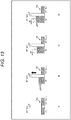
- Fig. 13 is a diagram explaining removal of kTC noise in the pixel 100 that performs the global shutter operation.
- the kTC noise at the time of reset can be reduced by the above operation, the potential of the FD becomes shallower than that of a normal pixel, and a transfer failure occurs.
- the FD wiring 251-1 and the control line 253-1 that supplies the control signal to the gate of the transfer transistor 102 are formed to run in parallel.
- the FD wiring 251-2 and the control line 253-2 connected to the control line 253-1 are formed to run in parallel.
- the transfer transistor 102 when the transfer transistor 102 is turned on, the potential of the FD can be boosted by the coupling, and the transfer failure due to the potential of the FD being shallower can be improved.
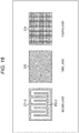
- Fig. 14 is a plan view showing an example of the wiring layout of adjacent wiring layers.
- a wiring 202-N having a predetermined potential and a fixed potential line 271-N are shown as wirings formed in the wiring layer of the Nth layer.
- the wiring 202-N is formed in a comb shape extending in the right-and-left direction in the drawing, and the fixed potential line 271-N is formed to have a comb-shaped portion facing the wiring 202-N and surround the wiring 202-N.
- a wiring 202-M having a predetermined potential and a fixed potential line 271-M are shown as wirings formed in the wiring layer of the N+1th or N-1th layer adjacent to the wiring layer of the Nth layer.
- the wiring 202-M is formed in a comb shape extending in the up-and-down direction in the drawing, and the fixed potential line 271-M is formed to have a comb-shaped portion facing the wiring 202-M and surround the wiring 202-M.
- the extension directions of the wiring 202-N and the fixed potential line 271-N of the wiring layer of the Nth layer and the wiring 202-M and the fixed potential line 271-M of the wiring layer of the N+1th or N-1th layer are perpendicular.
- the capacitance fluctuation in wiring capacitance formed by the wirings between the wiring layers becomes large when the wiring layout varies due to process variations.
- Fig. 15 is a diagram showing still another example of the cross section of the wiring layer of the pixel 100. Furthermore, Fig. 16 is a plan view showing an example of the wiring layout of the wiring layer of Fig. 15 .
- the wiring 202-2, the fixed potential line 271-2, and the like running in parallel are formed, and a solid wiring 373 is formed in the wiring layer M3, which is a layer above the wiring layer M2. Moreover, a solid wiring 374 connected to the fixed potential Vss is formed in the wiring layer M4, which is a layer above the wiring layer M3.
- Fig. 17 is a diagram showing another configuration example of the pixel 100.
- the pixel 100 of Fig. 17 is different from the pixel 100 of Fig. 2 in that it includes a conversion efficiency switching switch 401 and a capacitance 402 instead of the charge holding units 107, 108.
- a MOS transistor can be used for the conversion efficiency switching switch 401.
- One end of the conversion efficiency switching switch 401 is connected to the drain of the transfer transistor 102, the gate of the amplification transistor 105, and the source of the reset transistor 104, and another end is connected to a node 411 having a predetermined potential.
- the conversion efficiency switching switch 401 functions as a switch for switching the conversion efficiency. Furthermore, the capacitance 402 is formed by the wiring capacitance.
- the additional capacitance of the FD 103 is enabled or disabled by turning the conversion efficiency switching switch 401 on or off.
- the additional capacitance including the capacitance of the conversion efficiency switching switch 401 itself, the diffusion capacitance, and the wiring capacitance (capacitance 402) becomes enabled.
- the additional capacitance becomes disabled.
- the wiring layout according to the technology of the present disclosure can also be applied to the pixel 100 shown in Fig. 17 . Therefore, it becomes possible to increase the capacitance of the capacitance 402.
- the aforementioned solid-state imaging element 1 can be applied to various types of electronic device including an imaging system, e.g., a digital still camera or a digital video camera, a mobile phone with an imaging function, and other device with an imaging function.
- an imaging system e.g., a digital still camera or a digital video camera
- a mobile phone with an imaging function e.g., a smart phone, a smart phone, and other device with an imaging function.
- Fig. 18 is a block diagram showing a configuration example of an imaging apparatus, which is an electronic device to which the present disclosure has been applied.
- an imaging apparatus 501 includes an optical system 502, a solid-state imaging element 503, and a digital signal processor (DSP) 504, and the DSP 504, a display apparatus 505, an operation system 506, a memory 508, a recording apparatus 509, and a power system 510 are connected via a bus 507, enabling capturing of still images and moving images.
- DSP digital signal processor
- the optical system 502 includes one or a plurality of lenses and guides imaging light (incident light) from an object to the solid-state imaging element 503 to form an image on the light receiving surface (sensor unit) of the solid-state imaging element 503.
- a solid-state imaging element 1 having pixels 21 of any of the above-described configuration examples is applied. Electrons are accumulated in the solid-state imaging element 503 for a certain period of time according to the image formed on the light receiving surface through the optical system 502. Then, a signal corresponding to the electrons accumulated in the solid-state imaging element 503 is supplied to the DSP 504.
- the DSP 504 performs various signal processing on the signal from the solid-state imaging element 503 to acquire an image and causes the memory 508 to temporarily store the data of the image.
- the data of the image stored in the memory 508 is recorded in the recording apparatus 509 or supplied to and displayed on the display apparatus 505.
- the operation system 506 receives various operations by the user and supplies an operation signal to each block of the imaging apparatus 501, and the power system 510 supplies the electric power required for driving each block of the imaging apparatus 501.
- the imaging apparatus 501 configured in this way, by applying the solid-state imaging element 1 as described above as the solid-state imaging element 503, the capacitance of the charge holding unit can be increased and the kTC noise can be reduced, and it is possible to improve the image quality.
- the present disclosure may adopt the configuration described below.
Landscapes
- Engineering & Computer Science (AREA)
- Multimedia (AREA)
- Signal Processing (AREA)
- Solid State Image Pick-Up Elements (AREA)
- Transforming Light Signals Into Electric Signals (AREA)
- Internal Circuitry In Semiconductor Integrated Circuit Devices (AREA)
- Semiconductor Integrated Circuits (AREA)
- Control Of Motors That Do Not Use Commutators (AREA)
Abstract
Description
- The present disclosure relates to a solid-state imaging element and an electronic device, and more particularly to a solid-state imaging element and an electronic device capable of increasing the capacitance of a charge holding unit.
- Conventionally, there is an image sensor that performs global shutter type imaging in which all pixels simultaneously transfer charges from a photodiode (PD) to a floating diffusion (FD).
- Normally, it is known that kTC noise is generated at reset when driving an image sensor.
- On the other hand, for example,
Patent Document 1 discloses an image sensor that performs a global shutter type imaging including a charge holding unit different from the FD and feeding a signal potential including the kTC noise back to the FD to reduce the kTC noise. - Patent Document 1:
Japanese Patent Application Laid-Open No. 2018-64199 - In the configuration of
Patent Document 1, since the kTC noise is reduced by the capacitance distribution of the coupling capacitance between the charge holding unit and the FD, it is necessary to increase the capacitance of the charge holding unit, butPatent Document 1 does not disclose any specific configuration for increasing the capacitance of the charge holding unit. - The present disclosure has been made in view of such a situation, and is intended to increase the capacitance of the charge holding unit.
- The solid-state imaging element of the present disclosure is a solid-state imaging element including: a pixel including a photodiode, an FD that accumulates charges generated in the photodiode, and a charge holding unit that is connected in parallel with the FD, in which the charge holding unit includes a wiring capacitance formed by parallel running of a first wiring connected to a first potential and a second wiring connected to a second potential different from the first potential.
- The electronic device of the present disclosure is an electronic device including: a solid-state imaging element including a pixel including a photodiode, an FD that accumulates charges generated in the photodiode, and
a charge holding unit that is connected in parallel with the FD, in which the charge holding unit includes a wiring capacitance formed by parallel running of a first wiring connected to a first potential and a second wiring connected to a second potential different from the first potential. - According to the present disclosure, a pixel includes a photodiode, an FD that accumulates charges generated in the photodiode, and a charge holding unit that is connected in parallel with the FD, in which the charge holding unit includes a wiring capacitance formed by parallel running of a first wiring connected to a first potential and a second wiring connected to a second potential different from the first potential.
-
-
Fig. 1 is a diagram showing a configuration example of a solid-state imaging element to which the technology according to the present disclosure is applied. -
Fig. 2 is a diagram showing a configuration example of a pixel to which the technology according to the present disclosure is applied. -
Fig. 3 is a plan view showing an example of a wiring layout for forming a charge holding unit. -
Fig. 4 is a diagram showing a configuration example of a pixel according to a first embodiment of the present disclosure. -
Fig. 5 is a plan view showing an example of a wiring layout of a wiring layer of the first layer. -
Fig. 6 is a plan view showing an example of a wiring layout of a wiring layer of the second layer. -
Fig. 7 is a plan view showing an example of a wiring layout of a wiring layer of the third layer. -
Fig. 8 is a plan view showing an example of a wiring layout of a wiring layer of the fourth layer. -
Fig. 9 is a diagram showing an example of a cross section of a wiring layer. -
Fig. 10 is a diagram explaining a pixel of a second embodiment of the present disclosure. -
Fig. 11 is a diagram explaining a pixel of a third embodiment of the present disclosure. -
Fig. 12 is a diagram explaining a pixel of a fourth embodiment of the present disclosure. -
Fig. 13 is a diagram explaining a pixel of a fifth embodiment of the present disclosure. -
Fig. 14 is a diagram explaining a pixel of a sixth embodiment of the present disclosure. -
Fig. 15 is a diagram explaining a pixel of a seventh embodiment of the present disclosure. -
Fig. 16 is a diagram explaining a pixel of a seventh embodiment of the present disclosure. -
Fig. 17 is a diagram explaining a pixel of an eighth embodiment of the present disclosure. -
Fig. 18 is a diagram showing a configuration example of an electronic device to which the technology according to the present disclosure is applied. - Modes for carrying out the present disclosure (hereinafter, the embodiments) are described below. Note that description will be presented in the following order.
- 1. Outline of the technology according to the present disclosure
- 2. First embodiment (pixel configuration and wiring layout)
- 3. Second embodiment (example of wirings running in parallel directly above PD)
- 4. Third embodiment (example using High-K film)
- 5. Fourth embodiment (example of increasing the area of the diffusion layer)
- 6. Fifth embodiment (example of boosting the potential of FD)
- 7. Sixth embodiment (example of making wirings perpendicular between wiring layers)
- 8. Seventh embodiment (example of forming solid wiring)
- 9. Eighth embodiment (application to pixels for which conversion efficiency switching is performed)
- 10. Configuration example of electronic device
-
Fig. 1 is a diagram showing a configuration example of a solid-state imaging element 1 to which the technology according to the present disclosure is applied. - The solid-
state imaging element 1 includes apixel array unit 10, avertical drive unit 20, a columnsignal processing unit 30, a standardsignal supply unit 40, and a referencesignal generation unit 50. - The
pixel array unit 10 generates an image signal according to incident light. Thepixel array unit 10 includespixels 100 having a photoelectric conversion unit in a two-dimensional matrix. - In the
pixel array unit 10, acontrol line 11 for transmitting a control signal to thepixel 100 and avertical signal line 12 for transmitting an image signal generated by thepixel 100 are wired in an X-Y matrix. - The
control line 11 is wired for each row of a plurality ofpixels 100. Thecontrol line 11 is commonly wired to thepixels 100 arranged in one row. That is, control signals different with respect to each row are input to thepixels 100, and a common control signal is input to thepixels 100 arranged in one row. - On the other hand, the
vertical signal line 12 is wired for each column of the plurality ofpixels 100. Thevertical signal line 12 is commonly wired to thepixels 100 arranged in one column. That is, an image signal of thepixels 100 arranged in one column is transmitted via the commonvertical signal line 12. - The
vertical drive unit 20 generates a control signal and outputs it to thepixel array unit 10 via thecontrol line 11. - The column
signal processing unit 30 processes the image signal output from thepixel array unit 10. The image signal processed by the columnsignal processing unit 30 corresponds to an output signal of the solid-state imaging element 1, and is output to the outside of the solid-state imaging element 1. - The standard
signal supply unit 40 generates a standard signal. The standard signal is a signal that serves as a standard of the image signal generated by thepixel 100, and is, for example, a signal having a voltage corresponding to a black level image signal. The generated standard signal is supplied to the columnsignal processing unit 30 via astandard signal line 41. - The reference
signal generation unit 50 generates a reference signal. The reference signal is a signal serving as a standard for analog-to-digital conversion of the image signal generated by thepixel 100. As the reference signal, for example, a signal whose voltage drops like a lamp can be adopted. The generated reference signal is output to the columnsignal processing unit 30 via areference signal line 51. -
Fig. 2 is a diagram showing a configuration example of thepixel 100 to which the technology described above according to the present disclosure is applied. - The
pixel 100 includes a photodiode (PD) 101, atransfer transistor 102, a floating diffusion (FD) 103, areset transistor 104, anamplification transistor 105, and aselection transistor 106. - A MOS transistor can be used for each pixel transistor: the
transfer transistor 102, thereset transistor 104, theamplification transistor 105, and theselection transistor 106. - The
control line 11 and thevertical signal line 12 described above are wired to thepixel 100. Among the above, thecontrol line 11 includes a control line transfer gate (TRG), a control line reset (RST), and a control line select (SEL). These control lines are connected to the gate of the MOS transistor and transmit the control signal described inFig. 1 . When a voltage equal to or higher than a threshold voltage between the gate and the source of the MOS transistor is input to these control lines, the corresponding MOS transistor becomes conductive. - The control line TRG transmits a signal for controlling on/off of the
transfer transistor 102. The control line RST transmits a signal for controlling the reset of theFD 103. The control line SEL transmits a signal for selecting thepixel 100. - Moreover, a power line Vdd is wired to the
pixel 100. The power line Vdd supplies power with positive polarity. - The anode of the
PD 101 is grounded and the cathode is connected to the source of thetransfer transistor 102. The gate of thetransfer transistor 102 is connected to the control line TRG, and the drain is connected to one end of theFD 103, the gate of theamplification transistor 105, and the source of thereset transistor 104. Another end of theFD 103 is grounded. - The drain of the
reset transistor 104 is connected to the power line Vdd and the gate is connected to the control line RST. The drain of theamplification transistor 105 is connected to the power line Vdd and the source is connected to the drain of theselection transistor 106. The gate of theselection transistor 106 is connected to the control line SEL and the source is connected to thevertical signal line 12. - The
PD 101 generates a charge according to the emitted incident light by photoelectric conversion. - The
transfer transistor 102 transfers the charge generated by thePD 101 to theFD 103. Thetransfer transistor 102 transfers the charge by causing thePD 101 and theFD 103 to be conductive. - The
FD 103 accumulates the charge generated in thePD 101. TheFD 103 is formed in a diffusion layer of a semiconductor substrate such as a Si substrate and the like. - The
reset transistor 104 resets the charge accumulated in theFD 103. Thereset transistor 104 applies a power voltage to theFD 103 by conducting the power line Vdd and theFD 103, and resets theFD 103. - The
amplification transistor 105 detects a signal corresponding to the charge held in theFD 103 as a pixel signal. - The
selection transistor 106 outputs the image signal detected by theamplification transistor 105. Theselection transistor 106 outputs an image signal by causing theamplification transistor 105 and thevertical signal line 12 to be conductive. - With the above configuration, the
FD 103 is reset and the charge is transferred from thePD 101 to theFD 103 at the same time for all pixels. That is, the solid-state imaging element 1 can perform global shutter type imaging. - The
pixel 100 further includescharge holding units - The
charge holding units FD 103 and accumulate charges generated in thePD 101 apart from theFD 103. - One end of the
charge holding unit 107 is connected to the drain of thetransfer transistor 102, the gate of theamplification transistor 105, and the source of thereset transistor 104, and another end is connected to a node A having a predetermined potential. Furthermore, one end of thecharge holding unit 108 is connected to the node A, and another end is grounded. - Here, the
charge holding units -
Fig. 3 is a plan view showing an example of a wiring layout for forming thecharge holding units -
Fig. 3 shows the layout of a part of each of awiring 151 connected to the node A, aFD wiring 152 connecting the drain of thetransfer transistor 102 and the gate of theamplification transistor 105, and a fixedpotential line 153 connected to the fixed potential Vss different from the node A. Here, the fixed potential Vss is assumed to be a ground potential (GND). - As shown in
Fig. 3 , thewiring 151, theFD wiring 152, and the fixedpotential line 153 are laid out side by side so as to extend in the same direction (right-and-left direction in the drawing). In the following, the fact that wirings X, Y are laid out side by side means that the wirings X, Y run in parallel. - In the example of
Fig. 3 , thewiring 151 and the FD wiring 152 run in parallel to form thecharge holding unit 107, and thewiring 151 and the fixedpotential line 153 run in parallel to form thecharge holding unit 108. - With such a wiring layout, it is possible to increase the capacitance of the
charge holding units - Note that, in the example of
Fig. 3 , thewiring 151, theFD wiring 152, and the fixedpotential line 153 have only a straight portion extending in one direction (hereinafter referred to as an extending portion), but may have a portion bending or branching in a predetermined direction (hereinafter referred to as a bent portion). The bent portion can be formed in any of an L-shape, a T-shape, a U-shape, and a cross shape. - In this case, the two wirings may run in parallel, for example, such that the bent portion of each of the two wirings is bent in the same direction or the bent portion of another wiring is bent so as to surround at least a part of one wiring.
-
Fig. 4 is a diagram showing a configuration example of apixel 100 according to the first embodiment of the present disclosure. - The
pixel 100 ofFig. 4 differs from thepixel 100 ofFig. 2 in that it includes afeedback transistor 201. - A MOS transistor can be used as the
feedback transistor 201. - A control line feedback (FB) is further wired as a
control line 11 to thepixel 100 ofFig. 4 . The control line FB transmits a signal for controlling the supply of a reset voltage. The reset voltage is a voltage input to thepixel 100 when thepixel 100 is reset. - The source of the
feedback transistor 201 is connected to the drain of thereset transistor 104 and thenode 202 at a predetermined potential. The drain of thefeedback transistor 201 is connected to the columnsignal processing unit 30, and the gate is connected to the control line FB. - A
node 202 corresponds to the node A of thepixel 100 ofFig. 2 . Furthermore, in thepixel 100 ofFig. 4 ,charge holding units charge holding units pixel 100 ofFig. 2 are formed. - The
feedback transistor 201 causes thecharge holding unit 212 to hold the reset voltage output from the columnsignal processing unit 30. - The
charge holding unit 212 holds the reset voltage output from thefeedback transistor 201. - In the example of
Fig. 4 , thereset transistor 104 applies a reset voltage to theFD 103 by conducting thecharge holding unit 212 and theFD 103, and resets theFD 103. - The
charge holding unit 211 transmits the reset voltage held by thecharge holding unit 212 to theFD 103. - Normally, the kTC noise remains in the
FD 103 at the time of reset. The kTC noise is noise caused by the operation of thereset transistor 104, and is generated when thereset transistor 104 shifts from the conductive state to the nonconductive state. Then, a part of it remains in theFD 103. It is known that the kTC noise can be reduced by reducing the electrostatic capacitance of theFD 103. - In the
pixel 100 ofFig. 4 , thecharge holding units FD 103, and the capacitance of theFD 103 is distributed to thecharge holding units - Therefore, in the
pixel 100 ofFig. 4 , it is necessary to increase the capacitance of thecharge holding units pixel 100 of the present embodiment, the capacitance of thecharge holding units -
Figs. 5 to 8 are plan views showing an example of the wiring layout of the wiring layers of the first layer to the fourth layer corresponding to thepixel 100 ofFig. 4 . -
Fig. 5 shows the wiring layout of a wiring layer M1 of the first layer directly above the Si substrate on which thePD 101 and each pixel transistor are formed. - The
PD 101 is arranged substantially in the center of the Si substrate shown inFig. 5 , and thetransfer transistor 102 is formed in the upper left part thereof. Theamplification transistor 105 and theselection transistor 106 are formed side by side above thetransfer transistor 102 in the drawing. Thereset transistor 104 and thefeedback transistor 201 are formed side by side on the upper right side of thePD 101 in the drawing. - Note that the
reset transistor 104 and thefeedback transistor 201 are pixel transistors constituting apixel 100 corresponding to aPD 101, which is not shown, which is adjacent to the right side of thePD 101 shown inFig. 5 . Therefore, areset transistor 104 and afeedback transistor 201 constituting thepixel 100 corresponding to thePD 101 shown inFig. 5 are formed on the left side of thePD 101, which is not shown. - In
Fig. 5 , the wiring pattern of the wiring layer M1 is shown as a diagonal grid pattern. - A FD wiring 251-1 connecting the
transfer transistor 102 and theamplification transistor 105 is formed in the wiring layer M1. In the wiring layer M1, directly above thePD 101, alarge area pattern 252 for improving the sensitivity of thePD 101 by reflection of incident light is formed. - Furthermore, in the wiring layer M1, on the left side of the FD wiring 251-1 in the drawing, a control line 253-1 for supplying a control signal to the gate of the
transfer transistor 102 is formed. - The control line 253-1 is formed so that the extending portion and the bent portion, which are a part of the control line 253-1, run in parallel with the FD wiring 251-1.
- Moreover, in the wiring layer M1, at a position sandwiched between the
reset transistor 104 and thefeedback transistor 201, a wiring 202-1 for transmitting the potential of thenode 202 to the wiring layer above the second layer is formed. -
Fig. 6 shows the wiring layout of the wiring layer M2 of the second layer. - In
Fig. 6 , the wiring pattern of the wiring layer M2 is shown as a dot pattern. - In the wiring layer M2, a wiring 202-2 that is electrically connected to the wiring 202-1 through a via is formed from the position corresponding to the wiring 202-1 of the wiring layer M1. The wiring 202-2 is generally formed in an L shape.
- In the wiring layer M2, a fixed potential line 271-2a connected to a fixed potential Vss (GND) is formed above the wiring 202-2 in the drawing. The fixed potential line 271-2a is formed by combining an extending portion and a plurality of L-shaped, T-shaped, and U-shaped bent portions along the upper side of the wiring 202-2 in the drawing.
- The fixed potential line 271-2a is formed so that the extending portion and the bent portion, which are a part of the fixed potential line 271-2a, run in parallel with the wiring 202-2. Therefore, the wiring capacitance is formed between the wiring 202-2 connected to the
node 202 and the fixed potential line 271-2a connected to GND. - In the wiring layer M2, an FD wiring 251-2 electrically connected to the FD wiring 251-1 of the wiring layer M1 through a via is formed below the wiring 202-2 in the drawing. The FD wiring 251-2 is formed by combining an extending portion and a plurality of L-shaped, T-shaped, and U-shaped bent portions.
- The FD wiring 251-2 is formed so that the extending portion, which is a part of the FD wiring 251-2, runs in parallel with the wiring 202-2. Therefore, the wiring capacitance (coupling capacitance with the FD 103) is formed between the wiring 202-2 connected to the
node 202 and the FD wiring 251-2 connected to theFD 103. Note that, in the example ofFig. 6 , the wiring 202-2 and the FD wiring 251-2 are wirings corresponding to apixel 100, which is not shown, adjacent to the right side of thepixel 100 shown inFig. 6 . - In this way, by the wiring capacitance formed by the wiring 202-2, the fixed potential line 271-2a, and the FD wiring 251-2 running in parallel in the wiring layer M2, a high capacitance of the
charge holding units - Furthermore, in the wiring layer M2, a fixed potential line 271-2b connected to the fixed potential Vss is formed below the FD wiring 251-2 in the drawing. The fixed potential line 271-2b is formed by combining an extending portion and a plurality of L-shaped and U-shaped bent portions along the left side, the upper side, and the right side of the FD wiring 251-2 in the drawing.
- Moreover, in the upper right part of the wiring layer M2 in the drawing, a control line 253-2 that is electrically connected to the control line 253-1 of the wiring layer M1 through a via is formed. The control line 253-2 is generally formed in an L shape.
- The FD wiring 251-2 is formed so that the extending portion and the bent portion, which are a part of the FD wiring 251-2, run in parallel with the fixed potential line 271-2b and the control line 253-2. Therefore, a wiring capacitance is also formed between the FD wiring 251-2 connected to the
FD 103 and the fixed potential line 271-2b and the control line 253-2. - Here, as shown in
Fig. 6 , the wiring 202-2 and the FD wiring 251-2, which are the signal lines connected to theFD 103 and thecharge holding units -
Fig. 7 shows the wiring layout of the wiring layer M3 of the third layer. - In
Fig. 7 , the wiring pattern of the wiring layer M3 is shown as an upward-sloping diagonal pattern. As shown inFig. 7 , the wiring pattern of the wiring layer M3 is mainly formed so as to extend in the right-and-left direction in the drawing. - In the wiring layer M3, a wiring 202-3a that is electrically connected to the wiring 202-2 of the wiring layer M2 through a via is formed at the position corresponding to the substantially left half of the
PD 101. The wiring 202-3a is formed by combining an extending portion and a plurality of T-shaped and cross-shaped bent portions. - Similarly, in the wiring layer M3, a wiring 202-3b that is electrically connected to the wiring 202-2 of the wiring layer M2 through a via is formed at the position corresponding to the substantially right half of the
PD 101. The wiring 202-3b is formed by combining an extending portion and a plurality of L-shaped, T-shaped, and U-shaped bent portions. - Furthermore, in the wiring layer M3, a fixed potential line 271-3 connected to the fixed potential Vss is formed. The fixed potential line 271-3 is formed by combining an extending portion and a plurality of L-shaped, T-shaped, and cross-shaped bent portions so as to surround each of the four sides of the wiring 202-3a, 202-3b.
- In particular, the wirings 202-3a, 202-3b and the fixed potential line 271-3 are formed in a comb shape in which a part thereof faces each other.
- Moreover, in the wiring layer M3, above the wirings 202-3a, 202-3b and the fixed potential line 271-3 in the drawing, a control line 253-3 that is electrically connected to the control line 253-2 of the wiring layer M2 through a via is formed. The control line 253-3 is formed in a straight line extending in the right-and-left direction in the drawing.
- As described above, also in the wiring layer M3, the fixed potential line 271-3 is formed so that the extending portion and the bent portion, which are a part of the fixed potential line 271-3, run in parallel with the wirings 202-3a, 202-3b. Therefore, the wiring capacitance is formed between the wirings 202-3a, 202-3b connected to the
node 202 and the fixed potential line 271-3 connected to GND. - Also here, as shown in
Fig. 7 , the wirings 202-3a, 202-3b, which are the signal lines connected to thecharge holding units -
Fig. 8 shows the wiring layout of the wiring layer M4 of the fourth layer. - In
Fig. 8 , the wiring pattern of the wiring layer M4 is shown as a grid pattern. - In the wiring layer M4, fixed potential lines 271-4 connected to the fixed potential Vss are formed as a plurality of shielded wirings. A plurality of shielded fixed potential lines 271-4 is formed side by side in the right-and-left direction so as to extend in a straight line in the up-and-down direction in the drawing. Therefore, crosstalk between the signal lines connected to the
FD 103 and thecharge holding units - Note that the
pixel 100 includes the configuration in which a wiring capacitance is formed by wirings running in parallel in the same wiring layer, and also includes the configuration in which a wiring capacitance is formed between different wiring layers. -
Fig. 9 is a diagram showing an example of a cross section of a wiring layer of thepixel 100. -
Fig. 9 shows cross sections of aSi substrate 301 and wirings in the wiring layers M1 to M3. - On the
Si substrate 301, an N-type diffusion layer 310 serving as thenode 202 is formed within a large P-type diffusion layer formed. Thediffusion layer 310 formed on theSi substrate 301 and the wiring 202-1 of the wiring layer M1 are connected by acontact 311. Furthermore, the wiring 202-1 of the wiring layer M1 and the wiring 202-2 of the wiring layer M2 are connected by a via 312. - In the example of
Fig. 9 , within the wiring layer M2, the wiring 202-2 having a predetermined potential, the fixed potential line 271-2, and the FD wiring 251-2 run in parallel. Furthermore, within the wiring layer M3, the wiring 202-3 having a predetermined potential and the fixed potential line 271-3 run in parallel. - Moreover, in the example of
Fig. 9 , between the wiring layer M2 and the wiring layer M3, the wiring 202-2 having a predetermined potential and the fixed potential line 271-3 run in parallel, and the fixed potential line 271-2 and the wiring 202-3 having a predetermined potential run in parallel. - As described above, in the
pixel 100 of the present embodiment, the wiring capacitance is formed by running the wirings in parallel not only within the same wiring layer but also between different wiring layers. - According to the above configuration, the high capacitance of the charge holding unit connected in parallel with the FD can be realized by the wiring capacitance formed by the wiring connected to the node having a predetermined voltage, the fixed potential line, and the FD wiring running in parallel, and eventually the kTC noise can be reduced.
- Note that it is desirable that the wiring patterns of the wiring layers M1 to M4 described above are formed in the same wiring layout for all the
pixels 100. Therefore, the sensitivity non-uniformity between thepixels 100 can be reduced. - In a solid-state imaging element that performs global shutter type imaging, a read circuit cannot be shared between pixels. Therefore, it has been necessary to reduce the voltage amplitude of the pixel signal so that the pixel signal can be received in the subsequent circuit. For that purpose, it has been necessary to intentionally lower the conversion efficiency by increasing the capacitance of the FD.
- However, when the pixel size becomes small, the FD wiring routing area becomes narrow, so that it becomes difficult to increase the FD capacitance, and it becomes difficult to realize the intended conversion efficiency.
- On the other hand, in order to increase the quantum efficiency of the PD formed on the Si substrate in a case where the wavelength to be captured is a long wavelength, in the above-described embodiment, as described with reference to
Fig. 5 , thelarge area pattern 252 for improving the sensitivity of PD by the reflection of incident light is formed directly above the PD. - In the present embodiment, instead of the large area pattern, wirings running in parallel are formed directly above the PD.
-
Fig. 10 is a plan view showing another example of the wiring layout of the wiring layer M1 of the first layer corresponding to thepixel 100. - In the example of
Fig. 10 , in the wiring layer M1, the wiring 202-1 having a predetermined potential, the FD wiring 251-1, and the fixed potential line 271-1 are formed directly above thePD 101. - Directly above the
PD 101, the wiring 202-1 having a comb shape and a part of the FD wiring 251-1 having an L-shape are formed to run in parallel, and the fixed potential line 271-1 having a comb shape is formed to surround the wiring 202-1 and the FD wiring 251-1. In particular, the wiring 202-1 and the fixed potential line 271-1 are formed so that the comb-shaped portions face each other. - The wiring 202-1, the FD wiring 251-1, and the fixed potential line 271-1 directly above the
PD 101 are formed so that the L/S (line width of the pattern and the distance between the patterns) becomes narrower than the wavelength to be captured. - With such a configuration, even in a case where the pixel size is small, it is possible to improve the sensitivity of the PD by reflection of incident light and increase the capacitance of the FD and the charge holding unit.
- Note that, also in the example of
Fig. 10 , it is desirable that the wiring pattern of the wiring layer M1 is formed in the same wiring layout for all thepixels 100. Therefore, the sensitivity non-uniformity between thepixels 100 can be reduced. -
Fig. 11 is a diagram showing another example of the cross section of the wiring layer of thepixel 100. - In the example of
Fig. 11 , a high-k film 331 having a high dielectric constant is provided as an insulating film between the wirings forming the wiring capacitance in the wiring layers M2, M3. - Therefore, it is possible to increase the wiring capacitance formed by the wirings running in parallel.
- Note that, by not using a high-k film as an insulating film for a wiring layer (for example, wiring layer M4) in which wirings running in parallel are not formed (where it is not necessary to form a wiring capacitance), an unintended increase in wiring capacitance can be suppressed.
-
Fig. 12 is a diagram showing still another example of the cross section of the wiring layer of thepixel 100. - In the example of
Fig. 12 , a diffusion layer 310' is formed on theSi substrate 301 instead of thediffusion layer 310. The diffusion layer 310' is formed to have a larger area than thediffusion layer 351 forming the pixel transistor. - Moreover, the diffusion layer 310' may be formed by implanting ions having a concentration higher than that of the
diffusion layer 351 forming the pixel transistor. - Therefore, it is possible to increase the capacitance of the charge holding unit with a configuration other than running the wirings in parallel.
-
Fig. 13 is a diagram explaining removal of kTC noise in thepixel 100 that performs the global shutter operation. - First, as shown in A of
Fig. 13 , when the reset transistor (RST) is turned on, the potential of the FD is reset. - Next, as shown in B of
Fig. 13 , when the reset transistor (RST) is turned off, kTC noise (ΔVkTC) remains in the FD. - Thereafter, as shown in C of
Fig. 13 , when the feedback transistor (FB) is turned on, the potential of the FD and the standard signal are balanced, and the kTC noise remaining in the FD is removed. - Moreover, as shown in D of
Fig. 13 , when the feedback transistor (FB) is turned off, kTC noise (ΔV) remains in the FD again. However, the kTC noise is reduced by the capacitance distribution of the coupling capacitance between capacitance CFB of the charge holding unit and the capacitance of the FD. - Although the kTC noise at the time of reset can be reduced by the above operation, the potential of the FD becomes shallower than that of a normal pixel, and a transfer failure occurs.
- Therefore, in the wiring layer M1 of
Fig. 5 , the FD wiring 251-1 and the control line 253-1 that supplies the control signal to the gate of thetransfer transistor 102 are formed to run in parallel. - Furthermore, in the wiring layer M2 of
Fig. 6 , the FD wiring 251-2 and the control line 253-2 connected to the control line 253-1 are formed to run in parallel. - Therefore, when the
transfer transistor 102 is turned on, the potential of the FD can be boosted by the coupling, and the transfer failure due to the potential of the FD being shallower can be improved. -
Fig. 14 is a plan view showing an example of the wiring layout of adjacent wiring layers. - On the left side in
Fig. 14 , a wiring 202-N having a predetermined potential and a fixed potential line 271-N are shown as wirings formed in the wiring layer of the Nth layer. - The wiring 202-N is formed in a comb shape extending in the right-and-left direction in the drawing, and the fixed potential line 271-N is formed to have a comb-shaped portion facing the wiring 202-N and surround the wiring 202-N.
- On the right side in
Fig. 14 , a wiring 202-M having a predetermined potential and a fixed potential line 271-M are shown as wirings formed in the wiring layer of the N+1th or N-1th layer adjacent to the wiring layer of the Nth layer. - The wiring 202-M is formed in a comb shape extending in the up-and-down direction in the drawing, and the fixed potential line 271-M is formed to have a comb-shaped portion facing the wiring 202-M and surround the wiring 202-M.
- That is, the extension directions of the wiring 202-N and the fixed potential line 271-N of the wiring layer of the Nth layer and the wiring 202-M and the fixed potential line 271-M of the wiring layer of the N+1th or N-1th layer are perpendicular.
- For example, in a case where the extension directions of the wirings running in parallel are set to be the same direction between adjacent wiring layers, the capacitance fluctuation in wiring capacitance formed by the wirings between the wiring layers becomes large when the wiring layout varies due to process variations.
- On the other hand, as shown in
Fig. 14 , by making the extension directions of the wirings running in parallel perpendicular between the adjacent wiring layers, it is possible to reduce the capacitance fluctuation when the wiring layout varies due to process variations. -
Fig. 15 is a diagram showing still another example of the cross section of the wiring layer of thepixel 100. Furthermore,Fig. 16 is a plan view showing an example of the wiring layout of the wiring layer ofFig. 15 . - In the examples of
Figs. 15 and16 , the wiring 202-2, the fixed potential line 271-2, and the like running in parallel are formed, and asolid wiring 373 is formed in the wiring layer M3, which is a layer above the wiring layer M2. Moreover, asolid wiring 374 connected to the fixed potential Vss is formed in the wiring layer M4, which is a layer above the wiring layer M3. - Therefore, in addition to increasing the capacitance of the charge holding unit, it is possible to improve the sensitivity of the PD by reflection of incident light with the solid wiring.
-
Fig. 17 is a diagram showing another configuration example of thepixel 100. - The
pixel 100 ofFig. 17 is different from thepixel 100 ofFig. 2 in that it includes a conversionefficiency switching switch 401 and acapacitance 402 instead of thecharge holding units - A MOS transistor can be used for the conversion
efficiency switching switch 401. - One end of the conversion
efficiency switching switch 401 is connected to the drain of thetransfer transistor 102, the gate of theamplification transistor 105, and the source of thereset transistor 104, and another end is connected to anode 411 having a predetermined potential. - The conversion
efficiency switching switch 401 functions as a switch for switching the conversion efficiency. Furthermore, thecapacitance 402 is formed by the wiring capacitance. - The additional capacitance of the
FD 103 is enabled or disabled by turning the conversionefficiency switching switch 401 on or off. In a case where the conversionefficiency switching switch 401 is turned on, the additional capacitance including the capacitance of the conversionefficiency switching switch 401 itself, the diffusion capacitance, and the wiring capacitance (capacitance 402) becomes enabled. On the contrary, in a case where the conversionefficiency switching switch 401 is turned off, the additional capacitance becomes disabled. - The wiring layout according to the technology of the present disclosure can also be applied to the
pixel 100 shown inFig. 17 . Therefore, it becomes possible to increase the capacitance of thecapacitance 402. - For example, the aforementioned solid-
state imaging element 1 can be applied to various types of electronic device including an imaging system, e.g., a digital still camera or a digital video camera, a mobile phone with an imaging function, and other device with an imaging function. -
Fig. 18 is a block diagram showing a configuration example of an imaging apparatus, which is an electronic device to which the present disclosure has been applied. - As shown in
Fig. 18 , animaging apparatus 501 includes anoptical system 502, a solid-state imaging element 503, and a digital signal processor (DSP) 504, and theDSP 504, adisplay apparatus 505, anoperation system 506, amemory 508, arecording apparatus 509, and apower system 510 are connected via abus 507, enabling capturing of still images and moving images. - The
optical system 502 includes one or a plurality of lenses and guides imaging light (incident light) from an object to the solid-state imaging element 503 to form an image on the light receiving surface (sensor unit) of the solid-state imaging element 503. - As the solid-
state imaging element 503, a solid-state imaging element 1 having pixels 21 of any of the above-described configuration examples is applied. Electrons are accumulated in the solid-state imaging element 503 for a certain period of time according to the image formed on the light receiving surface through theoptical system 502. Then, a signal corresponding to the electrons accumulated in the solid-state imaging element 503 is supplied to theDSP 504. - The
DSP 504 performs various signal processing on the signal from the solid-state imaging element 503 to acquire an image and causes thememory 508 to temporarily store the data of the image. The data of the image stored in thememory 508 is recorded in therecording apparatus 509 or supplied to and displayed on thedisplay apparatus 505. Furthermore, theoperation system 506 receives various operations by the user and supplies an operation signal to each block of theimaging apparatus 501, and thepower system 510 supplies the electric power required for driving each block of theimaging apparatus 501. - In the
imaging apparatus 501 configured in this way, by applying the solid-state imaging element 1 as described above as the solid-state imaging element 503, the capacitance of the charge holding unit can be increased and the kTC noise can be reduced, and it is possible to improve the image quality. - Note that an embodiment of the present disclosure is not limited to the aforementioned embodiment, but various changes may be made within a scope without departing from the gist of the present disclosure.
- Moreover, the present disclosure may adopt the configuration described below.
- (1) A solid-state imaging element including:
- a pixel including
- a photodiode,
- an FD that accumulates charges generated in the photodiode, and
- a charge holding unit that is connected in parallel with the FD, in which
- the charge holding unit includes a wiring capacitance formed by parallel running of a first wiring connected to a first potential and a second wiring connected to a second potential different from the first potential.
- (2) The solid-state imaging element according to (1), in which
the first wiring and the second wiring have an extending portion extending in one direction and a bent portion bending in a predetermined direction. - (3) The solid-state imaging element according to (2), in which
the bent portion of the first wiring and the second wiring is formed in any of an L-shape, a T-shape, a U-shape, and a cross shape. - (4) The solid-state imaging element according to (3), in which
the first wiring and the second wiring are formed in one or more wiring layers, and
a part of the first wiring and the second wiring is formed directly above the photodiode. - (5) The solid-state imaging element according to (4), in which
a part of the first wiring and the second wiring is formed in the wiring layer of a first layer directly above a substrate. - (6) The solid-state imaging element according to (5), in which
a part of the first wiring and the second wiring is formed so that a line width and a distance are narrower than a wavelength to be captured. - (7) The solid-state imaging element according to (6), in which
each of a part of the first wiring and the second wiring is formed in a comb shape facing each other in a same wiring layer. - (8) The solid-state imaging element according to any of (4) to (7), in which
the second wiring is formed as at least one of an FD wiring connected to the FD, a fixed potential line, and a control line of a pixel transistor. - (9) The solid-state imaging element according to (8), in which
a potential of the fixed potential line includes GND. - (10) The solid-state imaging element according to (8) or (9), in which
the pixel transistor includes a transfer transistor. - (11) The solid-state imaging element according to any of (8) to (10), in which
the first wiring runs in parallel with the FD wiring to form a coupling capacitance with the FD. - (12) The solid-state imaging element according to (11), in which
the first wiring and the FD wiring are formed in a region surrounded by the fixed potential line or the control line. - (13) The solid-state imaging element according to (12), in which
the first wiring and the second wiring are formed in a same wiring layout in all the pixels. - (14) The solid-state imaging element according to (13), in which
the first wiring and the second wiring form the wiring capacitance in a same wiring layer. - (15) The solid-state imaging element according to (13), in which
the first wiring and the second wiring form the wiring capacitance between different wiring layers. - (16) The solid-state imaging element according to (13), in which
the first wiring and the second wiring form the wiring capacitance in a same wiring layer and between different wiring layers. - (17) The solid-state imaging element according to (13), in which
extension directions of the first wiring and the second wiring are perpendicular between adjacent wiring layers. - (18) The solid-state imaging element according to any of (13) to (17), in which
a high-k film is used as an insulating film between the first wiring and the second wiring. - (19) The solid-state imaging element according to any of (13) to (18), in which
a diffusion layer in a substrate connected to the first wiring has a larger area than another diffusion layer forming the pixel transistor. - (20) An electronic device including:
- a solid-state imaging element including
- a pixel including
- a photodiode,
- an FD that accumulates charges generated in the photodiode, and
- a charge holding unit that is connected in parallel with the FD, in which
- the charge holding unit includes a wiring capacitance formed by parallel running of a first wiring connected to a first potential and a second wiring connected to a second potential different from the first potential.
-
- 1
- Solid-state imaging element
- 100
- Pixel
- 101
- PD
- 102
- Transfer transistor
- 103
- FD
- 104
- Reset transistor
- 105
- Amplification transistor
- 106
- Selection transistor
- 107, 108
- Charge holding unit
- 201
- Feedback transistor
- 202
- Node
- 211, 212
- Charge holding unit
- 202-1, 202-2, 202-3
- Wiring
- 251-1, 251-2, 253-3
- FD wiring
- 253-1, 253-2
- Control line
- 271-1, 271-2, 273-3
- Fixed potential line
- 501
- Electronic device
- 503
- Solid-state imaging element
Claims (20)
- A solid-state imaging element comprising:a pixel includinga photodiode,an FD that accumulates charges generated in the photodiode, anda charge holding unit that is connected in parallel with the FD, whereinthe charge holding unit includes a wiring capacitance formed by parallel running of a first wiring connected to a first potential and a second wiring connected to a second potential different from the first potential.
- The solid-state imaging element according to claim 1, wherein
the first wiring and the second wiring have an extending portion extending in one direction and a bent portion bending in a predetermined direction. - The solid-state imaging element according to claim 2, wherein
the bent portion of the first wiring and the second wiring is formed in any of an L-shape, a T-shape, a U-shape, and a cross shape. - The solid-state imaging element according to claim 3, wherein
the first wiring and the second wiring are formed in one or more wiring layers, and
a part of the first wiring and the second wiring is formed directly above the photodiode. - The solid-state imaging element according to claim 4, wherein
a part of the first wiring and the second wiring is formed in the wiring layer of a first layer directly above a substrate. - The solid-state imaging element according to claim 5, wherein
a part of the first wiring and the second wiring is formed so that a line width and a distance are narrower than a wavelength to be captured. - The solid-state imaging element according to claim 6, wherein
each of a part of the first wiring and the second wiring is formed in a comb shape facing each other in a same wiring layer. - The solid-state imaging element according to claim 4, wherein
the second wiring is formed as at least one of an FD wiring connected to the FD, a fixed potential line, and a control line of a pixel transistor. - The solid-state imaging element according to claim 8, wherein
a potential of the fixed potential line includes GND. - The solid-state imaging element according to claim 8, wherein
the pixel transistor includes a transfer transistor. - The solid-state imaging element according to claim 8, wherein
the first wiring runs in parallel with the FD wiring to form a coupling capacitance with the FD. - The solid-state imaging element according to claim 11, wherein
the first wiring and the FD wiring are formed in a region surrounded by the fixed potential line or the control line. - The solid-state imaging element according to claim 12, wherein
the first wiring and the second wiring are formed in a same wiring layout in all the pixels. - The solid-state imaging element according to claim 13, wherein
the first wiring and the second wiring form the wiring capacitance in a same wiring layer. - The solid-state imaging element according to claim 13, wherein
the first wiring and the second wiring form the wiring capacitance between different wiring layers. - The solid-state imaging element according to claim 13, wherein
the first wiring and the second wiring form the wiring capacitance in a same wiring layer and between different wiring layers. - The solid-state imaging element according to claim 13, wherein
extension directions of the first wiring and the second wiring are perpendicular between adjacent wiring layers. - The solid-state imaging element according to claim 13, wherein
a high-k film is used as an insulating film between the first wiring and the second wiring. - The solid-state imaging element according to claim 13, wherein
a diffusion layer in a substrate connected to the first wiring has a larger area than another diffusion layer forming the pixel transistor. - An electronic device comprising:a solid-state imaging element includinga pixel includinga photodiode,an FD that accumulates charges generated in the photodiode, anda charge holding unit that is connected in parallel with the FD, whereinthe charge holding unit includes a wiring capacitance formed by parallel running of a first wiring connected to a first potential and a second wiring connected to a second potential different from the first potential.
Applications Claiming Priority (2)
| Application Number | Priority Date | Filing Date | Title |
|---|---|---|---|
| JP2018174517 | 2018-09-19 | ||
| PCT/JP2019/034901 WO2020059510A1 (en) | 2018-09-19 | 2019-09-05 | Solid-state imaging element and electronic device |
Publications (3)
| Publication Number | Publication Date |
|---|---|
| EP3855497A1 true EP3855497A1 (en) | 2021-07-28 |
| EP3855497A4 EP3855497A4 (en) | 2021-11-24 |
| EP3855497B1 EP3855497B1 (en) | 2025-03-19 |
Family
ID=69887386
Family Applications (1)
| Application Number | Title | Priority Date | Filing Date |
|---|---|---|---|
| EP19863094.9A Active EP3855497B1 (en) | 2018-09-19 | 2019-09-05 | Solid-state imaging element and electronic device |
Country Status (6)
| Country | Link |
|---|---|
| US (2) | US12087799B2 (en) |
| EP (1) | EP3855497B1 (en) |
| JP (2) | JP7368371B2 (en) |
| CN (3) | CN112703599B (en) |
| TW (2) | TWI822858B (en) |
| WO (1) | WO2020059510A1 (en) |
Families Citing this family (10)
| Publication number | Priority date | Publication date | Assignee | Title |
|---|---|---|---|---|
| JP7368371B2 (en) * | 2018-09-19 | 2023-10-24 | ソニーセミコンダクタソリューションズ株式会社 | Solid-state image sensor and electronic equipment |
| JP2022070502A (en) * | 2020-10-27 | 2022-05-13 | ソニーセミコンダクタソリューションズ株式会社 | Imaging device and electronic apparatus |
| JP2022104203A (en) | 2020-12-28 | 2022-07-08 | ソニーセミコンダクタソリューションズ株式会社 | Image sensor and image sensor |
| US12288782B2 (en) * | 2022-02-24 | 2025-04-29 | Globalfoundries U.S. Inc. | Cell layouts |
| US20250234110A1 (en) * | 2022-03-31 | 2025-07-17 | Sony Semiconductor Solutions Corporation | Imaging element, imaging apparatus, and semiconductor element |
| JPWO2025033456A1 (en) | 2023-08-07 | 2025-02-13 | ||
| WO2025142235A1 (en) * | 2023-12-25 | 2025-07-03 | ソニーセミコンダクタソリューションズ株式会社 | Light detection device |
| WO2025169617A1 (en) * | 2024-02-08 | 2025-08-14 | ソニーセミコンダクタソリューションズ株式会社 | Capacitive element, and display device |
| JP2025155161A (en) | 2024-04-01 | 2025-10-14 | オムニヴィジョン テクノロジーズ インコーポレイテッド | Image sensor and method for manufacturing the same |
| WO2026023245A1 (en) * | 2024-07-22 | 2026-01-29 | ソニーセミコンダクタソリューションズ株式会社 | Solid-state imaging device |
Family Cites Families (15)
| Publication number | Priority date | Publication date | Assignee | Title |
|---|---|---|---|---|
| KR20040093905A (en) * | 2003-04-30 | 2004-11-09 | 매그나칩 반도체 유한회사 | Unit pixel for high sensitive cmos image sensor |
| JP4067054B2 (en) | 2004-02-13 | 2008-03-26 | キヤノン株式会社 | Solid-state imaging device and imaging system |
| KR100922931B1 (en) * | 2006-12-27 | 2009-10-22 | 동부일렉트로닉스 주식회사 | CMOS image sensor and its manufacturing method |
| JP5422455B2 (en) | 2010-03-23 | 2014-02-19 | パナソニック株式会社 | Solid-state imaging device |
| JP2011204797A (en) * | 2010-03-24 | 2011-10-13 | Sony Corp | Solid-state imaging apparatus, method of manufacturing the same, and electronic equipment |
| JP5126291B2 (en) | 2010-06-07 | 2013-01-23 | 株式会社ニコン | Solid-state image sensor |
| JP6024103B2 (en) | 2011-06-30 | 2016-11-09 | ソニー株式会社 | Image sensor, image sensor drive method, image sensor manufacturing method, and electronic device |
| JP2014112580A (en) * | 2012-12-05 | 2014-06-19 | Sony Corp | Solid-state image sensor and driving method |
| JP2014060519A (en) * | 2012-09-14 | 2014-04-03 | Sony Corp | Solid-state image sensor, control method thereof and electronic apparatus |
| JP2015056878A (en) | 2013-09-13 | 2015-03-23 | 株式会社東芝 | Solid-state imaging device |
| US9398237B2 (en) | 2014-04-30 | 2016-07-19 | Sony Corporation | Image sensor with floating diffusion interconnect capacitor |
| TWI701819B (en) | 2015-06-09 | 2020-08-11 | 日商索尼半導體解決方案公司 | Imaging element, driving method and electronic equipment |
| US9942503B2 (en) | 2016-02-23 | 2018-04-10 | Semiconductor Components Industries, Llc | Image sensors having high-efficiency charge storage capabilities |
| JP6886267B2 (en) | 2016-10-13 | 2021-06-16 | ソニーセミコンダクタソリューションズ株式会社 | Image sensor and image sensor |
| JP7368371B2 (en) * | 2018-09-19 | 2023-10-24 | ソニーセミコンダクタソリューションズ株式会社 | Solid-state image sensor and electronic equipment |
-
2019
- 2019-09-05 JP JP2020548300A patent/JP7368371B2/en active Active
- 2019-09-05 CN CN201980059756.4A patent/CN112703599B/en active Active
- 2019-09-05 CN CN202311416510.2A patent/CN117459847A/en active Pending
- 2019-09-05 US US17/273,585 patent/US12087799B2/en active Active
- 2019-09-05 WO PCT/JP2019/034901 patent/WO2020059510A1/en not_active Ceased
- 2019-09-05 EP EP19863094.9A patent/EP3855497B1/en active Active
- 2019-09-05 CN CN202311413680.5A patent/CN117459846A/en active Pending
- 2019-09-12 TW TW108132914A patent/TWI822858B/en active
- 2019-09-12 TW TW112141505A patent/TWI913601B/en active
-
2023
- 2023-10-12 JP JP2023176500A patent/JP7834074B2/en active Active
-
2024
- 2024-07-12 US US18/770,882 patent/US20240363669A1/en active Pending
Also Published As
| Publication number | Publication date |
|---|---|
| US12087799B2 (en) | 2024-09-10 |
| TW202017361A (en) | 2020-05-01 |
| TWI822858B (en) | 2023-11-21 |
| CN112703599B (en) | 2024-10-18 |
| TW202433736A (en) | 2024-08-16 |
| JP7834074B2 (en) | 2026-03-23 |
| EP3855497B1 (en) | 2025-03-19 |
| CN112703599A (en) | 2021-04-23 |
| EP3855497A4 (en) | 2021-11-24 |
| CN117459846A (en) | 2024-01-26 |
| US20210343777A1 (en) | 2021-11-04 |
| JP7368371B2 (en) | 2023-10-24 |
| CN117459847A (en) | 2024-01-26 |
| JP2023178357A (en) | 2023-12-14 |
| WO2020059510A1 (en) | 2020-03-26 |
| US20240363669A1 (en) | 2024-10-31 |
| JPWO2020059510A1 (en) | 2021-09-02 |
| TWI913601B (en) | 2026-02-01 |
Similar Documents
| Publication | Publication Date | Title |
|---|---|---|
| EP3855497B1 (en) | Solid-state imaging element and electronic device | |
| US9253425B2 (en) | Photo-electric conversion device for current fluctuation suppression | |
| US11153515B2 (en) | Solid state image sensor comprising stacked substrates, semiconductor device, and electronic device | |
| JP4553612B2 (en) | Image pickup device and image pickup apparatus including the same | |
| US10229942B2 (en) | Solid state imaging device and electronic apparatus | |
| US9596426B2 (en) | Imaging device, imaging system, and method for driving imaging device | |
| CN103858235B (en) | Solid State Image Sensors and Electronics | |
| JP5813047B2 (en) | Imaging device and imaging system. | |
| CN116802811A (en) | Image pickup element and image pickup device | |
| CN113675225B (en) | Image sensing device | |
| KR20160137953A (en) | Solid-state imaging element and imaging device | |
| US9202831B2 (en) | Imaging apparatus and imaging system | |
| CN113224087A (en) | Image sensing device | |
| CN116112816A (en) | Pixel array and device including same | |
| JP6526159B2 (en) | Solid-state imaging device and camera | |
| CN116980769A (en) | Solid-state imaging device, driving method of solid-state imaging device, and electronic apparatus | |
| US9659988B2 (en) | Image pickup apparatus | |
| JP4553969B2 (en) | Imaging device | |
| JP2017103429A (en) | Imaging apparatus and imaging system | |
| JP2010034576A (en) | Imaging device | |
| JP2010135840A (en) | Imaging device |
Legal Events
| Date | Code | Title | Description |
|---|---|---|---|
| STAA | Information on the status of an ep patent application or granted ep patent |
Free format text: STATUS: THE INTERNATIONAL PUBLICATION HAS BEEN MADE |
|
| PUAI | Public reference made under article 153(3) epc to a published international application that has entered the european phase |
Free format text: ORIGINAL CODE: 0009012 |
|
| STAA | Information on the status of an ep patent application or granted ep patent |
Free format text: STATUS: REQUEST FOR EXAMINATION WAS MADE |
|
| 17P | Request for examination filed |
Effective date: 20210310 |
|
| AK | Designated contracting states |
Kind code of ref document: A1 Designated state(s): AL AT BE BG CH CY CZ DE DK EE ES FI FR GB GR HR HU IE IS IT LI LT LU LV MC MK MT NL NO PL PT RO RS SE SI SK SM TR |
|
| A4 | Supplementary search report drawn up and despatched |
Effective date: 20211022 |
|
| RIC1 | Information provided on ipc code assigned before grant |
Ipc: H04N 5/3745 20110101ALI20211018BHEP Ipc: H01L 31/10 20060101ALI20211018BHEP Ipc: H01L 23/522 20060101ALI20211018BHEP Ipc: H01L 21/768 20060101ALI20211018BHEP Ipc: H01L 21/3205 20060101ALI20211018BHEP Ipc: H01L 27/146 20060101AFI20211018BHEP |
|
| DAV | Request for validation of the european patent (deleted) | ||
| DAX | Request for extension of the european patent (deleted) | ||
| GRAP | Despatch of communication of intention to grant a patent |
Free format text: ORIGINAL CODE: EPIDOSNIGR1 |
|
| STAA | Information on the status of an ep patent application or granted ep patent |
Free format text: STATUS: GRANT OF PATENT IS INTENDED |
|
| RIC1 | Information provided on ipc code assigned before grant |
Ipc: H04N 25/616 20230101ALI20241002BHEP Ipc: H04N 25/532 20230101ALI20241002BHEP Ipc: H04N 25/771 20230101ALI20241002BHEP Ipc: H01L 27/146 20060101AFI20241002BHEP |
|
| INTG | Intention to grant announced |
Effective date: 20241024 |
|
| GRAS | Grant fee paid |
Free format text: ORIGINAL CODE: EPIDOSNIGR3 |
|
| GRAA | (expected) grant |
Free format text: ORIGINAL CODE: 0009210 |
|
| STAA | Information on the status of an ep patent application or granted ep patent |
Free format text: STATUS: THE PATENT HAS BEEN GRANTED |
|
| AK | Designated contracting states |
Kind code of ref document: B1 Designated state(s): AL AT BE BG CH CY CZ DE DK EE ES FI FR GB GR HR HU IE IS IT LI LT LU LV MC MK MT NL NO PL PT RO RS SE SI SK SM TR |
|
| P01 | Opt-out of the competence of the unified patent court (upc) registered |
Free format text: CASE NUMBER: APP_6759/2025 Effective date: 20250210 |
|
| REG | Reference to a national code |
Ref country code: GB Ref legal event code: FG4D |
|
| REG | Reference to a national code |
Ref country code: IE Ref legal event code: FG4D |
|
| REG | Reference to a national code |
Ref country code: DE Ref legal event code: R096 Ref document number: 602019067587 Country of ref document: DE |
|
| REG | Reference to a national code |
Ref country code: NL Ref legal event code: FP |
|
| PG25 | Lapsed in a contracting state [announced via postgrant information from national office to epo] |
Ref country code: RS Free format text: LAPSE BECAUSE OF FAILURE TO SUBMIT A TRANSLATION OF THE DESCRIPTION OR TO PAY THE FEE WITHIN THE PRESCRIBED TIME-LIMIT Effective date: 20250619 |
|
| PG25 | Lapsed in a contracting state [announced via postgrant information from national office to epo] |
Ref country code: FI Free format text: LAPSE BECAUSE OF FAILURE TO SUBMIT A TRANSLATION OF THE DESCRIPTION OR TO PAY THE FEE WITHIN THE PRESCRIBED TIME-LIMIT Effective date: 20250319 |
|
| REG | Reference to a national code |
Ref country code: LT Ref legal event code: MG9D |
|
| PG25 | Lapsed in a contracting state [announced via postgrant information from national office to epo] |
Ref country code: NO Free format text: LAPSE BECAUSE OF FAILURE TO SUBMIT A TRANSLATION OF THE DESCRIPTION OR TO PAY THE FEE WITHIN THE PRESCRIBED TIME-LIMIT Effective date: 20250619 |
|
| PG25 | Lapsed in a contracting state [announced via postgrant information from national office to epo] |
Ref country code: HR Free format text: LAPSE BECAUSE OF FAILURE TO SUBMIT A TRANSLATION OF THE DESCRIPTION OR TO PAY THE FEE WITHIN THE PRESCRIBED TIME-LIMIT Effective date: 20250319 |
|
| PG25 | Lapsed in a contracting state [announced via postgrant information from national office to epo] |
Ref country code: LV Free format text: LAPSE BECAUSE OF FAILURE TO SUBMIT A TRANSLATION OF THE DESCRIPTION OR TO PAY THE FEE WITHIN THE PRESCRIBED TIME-LIMIT Effective date: 20250319 |
|
| PG25 | Lapsed in a contracting state [announced via postgrant information from national office to epo] |
Ref country code: BG Free format text: LAPSE BECAUSE OF FAILURE TO SUBMIT A TRANSLATION OF THE DESCRIPTION OR TO PAY THE FEE WITHIN THE PRESCRIBED TIME-LIMIT Effective date: 20250319 Ref country code: GR Free format text: LAPSE BECAUSE OF FAILURE TO SUBMIT A TRANSLATION OF THE DESCRIPTION OR TO PAY THE FEE WITHIN THE PRESCRIBED TIME-LIMIT Effective date: 20250620 |
|
| REG | Reference to a national code |
Ref country code: AT Ref legal event code: MK05 Ref document number: 1777723 Country of ref document: AT Kind code of ref document: T Effective date: 20250319 |
|
| PG25 | Lapsed in a contracting state [announced via postgrant information from national office to epo] |
Ref country code: SE Free format text: LAPSE BECAUSE OF FAILURE TO SUBMIT A TRANSLATION OF THE DESCRIPTION OR TO PAY THE FEE WITHIN THE PRESCRIBED TIME-LIMIT Effective date: 20250319 |
|
| PGFP | Annual fee paid to national office [announced via postgrant information from national office to epo] |
Ref country code: NL Payment date: 20250820 Year of fee payment: 7 |
|
| PG25 | Lapsed in a contracting state [announced via postgrant information from national office to epo] |
Ref country code: SM Free format text: LAPSE BECAUSE OF FAILURE TO SUBMIT A TRANSLATION OF THE DESCRIPTION OR TO PAY THE FEE WITHIN THE PRESCRIBED TIME-LIMIT Effective date: 20250319 |
|
| PG25 | Lapsed in a contracting state [announced via postgrant information from national office to epo] |
Ref country code: ES Free format text: LAPSE BECAUSE OF FAILURE TO SUBMIT A TRANSLATION OF THE DESCRIPTION OR TO PAY THE FEE WITHIN THE PRESCRIBED TIME-LIMIT Effective date: 20250319 Ref country code: PT Free format text: LAPSE BECAUSE OF FAILURE TO SUBMIT A TRANSLATION OF THE DESCRIPTION OR TO PAY THE FEE WITHIN THE PRESCRIBED TIME-LIMIT Effective date: 20250721 |
|
| PGFP | Annual fee paid to national office [announced via postgrant information from national office to epo] |
Ref country code: DE Payment date: 20250820 Year of fee payment: 7 |
|
| PG25 | Lapsed in a contracting state [announced via postgrant information from national office to epo] |
Ref country code: IT Free format text: LAPSE BECAUSE OF FAILURE TO SUBMIT A TRANSLATION OF THE DESCRIPTION OR TO PAY THE FEE WITHIN THE PRESCRIBED TIME-LIMIT Effective date: 20250319 Ref country code: PL Free format text: LAPSE BECAUSE OF FAILURE TO SUBMIT A TRANSLATION OF THE DESCRIPTION OR TO PAY THE FEE WITHIN THE PRESCRIBED TIME-LIMIT Effective date: 20250319 |
|
| PG25 | Lapsed in a contracting state [announced via postgrant information from national office to epo] |
Ref country code: AT Free format text: LAPSE BECAUSE OF FAILURE TO SUBMIT A TRANSLATION OF THE DESCRIPTION OR TO PAY THE FEE WITHIN THE PRESCRIBED TIME-LIMIT Effective date: 20250319 |
|
| PG25 | Lapsed in a contracting state [announced via postgrant information from national office to epo] |
Ref country code: CZ Free format text: LAPSE BECAUSE OF FAILURE TO SUBMIT A TRANSLATION OF THE DESCRIPTION OR TO PAY THE FEE WITHIN THE PRESCRIBED TIME-LIMIT Effective date: 20250319 Ref country code: EE Free format text: LAPSE BECAUSE OF FAILURE TO SUBMIT A TRANSLATION OF THE DESCRIPTION OR TO PAY THE FEE WITHIN THE PRESCRIBED TIME-LIMIT Effective date: 20250319 |
|
| PG25 | Lapsed in a contracting state [announced via postgrant information from national office to epo] |
Ref country code: RO Free format text: LAPSE BECAUSE OF FAILURE TO SUBMIT A TRANSLATION OF THE DESCRIPTION OR TO PAY THE FEE WITHIN THE PRESCRIBED TIME-LIMIT Effective date: 20250319 |
|
| PG25 | Lapsed in a contracting state [announced via postgrant information from national office to epo] |
Ref country code: SK Free format text: LAPSE BECAUSE OF FAILURE TO SUBMIT A TRANSLATION OF THE DESCRIPTION OR TO PAY THE FEE WITHIN THE PRESCRIBED TIME-LIMIT Effective date: 20250319 |
|
| PG25 | Lapsed in a contracting state [announced via postgrant information from national office to epo] |
Ref country code: IS Free format text: LAPSE BECAUSE OF FAILURE TO SUBMIT A TRANSLATION OF THE DESCRIPTION OR TO PAY THE FEE WITHIN THE PRESCRIBED TIME-LIMIT Effective date: 20250719 |
|
| REG | Reference to a national code |
Ref country code: DE Ref legal event code: R097 Ref document number: 602019067587 Country of ref document: DE |
|
| PG25 | Lapsed in a contracting state [announced via postgrant information from national office to epo] |
Ref country code: DK Free format text: LAPSE BECAUSE OF FAILURE TO SUBMIT A TRANSLATION OF THE DESCRIPTION OR TO PAY THE FEE WITHIN THE PRESCRIBED TIME-LIMIT Effective date: 20250319 |
|
| PLBE | No opposition filed within time limit |
Free format text: ORIGINAL CODE: 0009261 |
|
| STAA | Information on the status of an ep patent application or granted ep patent |
Free format text: STATUS: NO OPPOSITION FILED WITHIN TIME LIMIT |
|
| REG | Reference to a national code |
Ref country code: CH Ref legal event code: L10 Free format text: ST27 STATUS EVENT CODE: U-0-0-L10-L00 (AS PROVIDED BY THE NATIONAL OFFICE) Effective date: 20260128 |
|
| 26N | No opposition filed |
Effective date: 20251222 |
|
| REG | Reference to a national code |
Ref country code: CH Ref legal event code: H13 Free format text: ST27 STATUS EVENT CODE: U-0-0-H10-H13 (AS PROVIDED BY THE NATIONAL OFFICE) Effective date: 20260504 |