EP3855483A1 - Through-interposer connections using blind vias - Google Patents
Through-interposer connections using blind vias Download PDFInfo
- Publication number
- EP3855483A1 EP3855483A1 EP20305044.8A EP20305044A EP3855483A1 EP 3855483 A1 EP3855483 A1 EP 3855483A1 EP 20305044 A EP20305044 A EP 20305044A EP 3855483 A1 EP3855483 A1 EP 3855483A1
- Authority
- EP
- European Patent Office
- Prior art keywords
- substrate
- interposer
- resistivity portion
- blind via
- resistivity
- Prior art date
- Legal status (The legal status is an assumption and is not a legal conclusion. Google has not performed a legal analysis and makes no representation as to the accuracy of the status listed.)
- Granted
Links
Images

Classifications
-
- H—ELECTRICITY
- H10—SEMICONDUCTOR DEVICES; ELECTRIC SOLID-STATE DEVICES NOT OTHERWISE PROVIDED FOR
- H10W—GENERIC PACKAGES, INTERCONNECTIONS, CONNECTORS OR OTHER CONSTRUCTIONAL DETAILS OF DEVICES COVERED BY CLASS H10
- H10W70/00—Package substrates; Interposers; Redistribution layers [RDL]
- H10W70/60—Insulating or insulated package substrates; Interposers; Redistribution layers
- H10W70/67—Insulating or insulated package substrates; Interposers; Redistribution layers characterised by their insulating layers or insulating parts
- H10W70/69—Insulating materials thereof
- H10W70/698—Semiconductor materials that are electrically insulating, e.g. undoped silicon
-
- H—ELECTRICITY
- H01—ELECTRIC ELEMENTS
- H01S—DEVICES USING THE PROCESS OF LIGHT AMPLIFICATION BY STIMULATED EMISSION OF RADIATION [LASER] TO AMPLIFY OR GENERATE LIGHT; DEVICES USING STIMULATED EMISSION OF ELECTROMAGNETIC RADIATION IN WAVE RANGES OTHER THAN OPTICAL
- H01S5/00—Semiconductor lasers
- H01S5/02—Structural details or components not essential to laser action
- H01S5/022—Mountings; Housings
- H01S5/023—Mount members, e.g. sub-mount members
- H01S5/02315—Support members, e.g. bases or carriers
-
- H—ELECTRICITY
- H10—SEMICONDUCTOR DEVICES; ELECTRIC SOLID-STATE DEVICES NOT OTHERWISE PROVIDED FOR
- H10W—GENERIC PACKAGES, INTERCONNECTIONS, CONNECTORS OR OTHER CONSTRUCTIONAL DETAILS OF DEVICES COVERED BY CLASS H10
- H10W70/00—Package substrates; Interposers; Redistribution layers [RDL]
- H10W70/60—Insulating or insulated package substrates; Interposers; Redistribution layers
- H10W70/62—Insulating or insulated package substrates; Interposers; Redistribution layers characterised by their interconnections
- H10W70/63—Vias, e.g. via plugs
- H10W70/635—Through-vias
Definitions
- the present invention relates to the field of interposers as well as to methods of fabricating interposers and a technique for achieving electrical interconnection through an interposer.
- optical interposers are in wide-spread use, for example as part of optical interconnects used in data centres.
- An optical interposer generally includes a substrate that is mounted on a mounting substrate, and elements such as a transmission line are provided on a surface of the interposer substrate that is remote from the mounting substrate.
- the interposer substrate generally is configured as an electrical insulator or is a substrate (e.g. high-resistivity (HR) silicon) having sufficiently high resistivity to prevent undesired current leakage.
- HR high-resistivity
- a transmitter optical sub-assembly (TOSA) in a transceiver module may include four optical interposers disposed side by side.
- TOSA transmitter optical sub-assembly
- Fig.2 illustrates how insertion loss varies with frequency in the TOSA illustrated in Fig.1 . It can be seen from Fig.2 that there are insertion loss peaks at the frequency positions indicated by the arrows A.
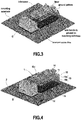
- Fig.3 is a schematic representation of an individual interposer having wire bonds connecting a grounding pattern on the interposer to ground on the mounting substrate.
- cross-talk may be generated between the bonding wires themselves.
- the impedance of these wire bonds is non-negligible.
- its impedance and particularly the inductive behaviour of the wire bonds can be decreased by reducing their length. From an integration point of view, this is more efficient than increasing the section of the ground return path.
- TSVs through-silicon vias
- the thickness of the interposer is relatively large (>500 ⁇ m)) in order to achieve necessary optical alignment of the laser, and this would necessitate use of a long TSV.
- the allowable aspect ratio of a TSV there are limitations on the allowable aspect ratio of a TSV and so, if the TSV is long, then the footprint occupied on the circuit board (i.e. the cross-sectional surface area of the TSV) would be large and this is incompatible with achieving a high degree of integration.
- TSVs are generally filled with metals that have a coefficient of thermal expansion which is quite different from the coefficient of thermal expansion of the interposer substrate, leading to undesired stresses in the interposer substrate.
- specific manufacturing steps are required in order to define, form and fill TSVs, additional to the manufacturing steps required to create the interposer and the circuit elements thereon.
- use of TSVs for grounding can lead to increased complexity in the manufacturing process.
- the present invention has been made in the light of the above-described issues.
- the present invention provides an interposer comprising:
- This electrically-conductive structure may be composed of a simple electrically-conductive layer provided at the sidewall of the blind via-hole but the invention is not limited to this case.
- a multi-layer may be provided at the sidewall, this multi-layer comprising a highly-resistive material on its outer periphery overlaid with one, or several, layers having different conductivities (closer to the axis of the via-hole).
- the conductive layer may comprise a stacked combination of conductive and insulating layers following the implementation of a MIM structure of the adjacent capacitor.
- a common set of process steps can be used to form the capacitor MIM structure and the electrically-conductive structure in the blind via-hole, thus avoiding increase in the complexity and cost of the manufacturing process.
- the high-resistivity portion of the composite substrate used in the above-described interposer prevents current leakage between elements (e.g. a transmission line) formed on the first surface of the interposer and the mounting substrate upon which the interposer is mounted in use.
- the low-resistivity portion of the composite substrate used in the above-described interposer cooperates with conductive material in the blind via-hole(s) to establish a top-to-bottom connection structure through the interposer substrate.
- the present invention finds application not only for the purposes of establishing a grounding path through an interposer but also for other purposes.
- the techniques of the present invention may usefully be applied in cases where it is desired to build high Q inductances on the same interposer, in cases where it is desired to manage electrically-independent GND domains on a common interposer, etc.
- an interposer can establish a direct conductive path, for example between the interposer grounding pattern (die ground) and the ground of a mounting substrate upon which the interposer is mounted in use, through the die itself. This shortens the length of the electrical connection. Accordingly, in the case of using the through-interposer connection for grounding, the length of the ground connection between the interposer and the mounting substrate is reduced, and the uniformity of the ground potential is increased.
- the above-described interposer structure enables grounding to be achieved without using bonding wires for this purpose. Accordingly, no extra footprint on the mounting substrate is required.
- the above-described interposer structure enables grounding to be achieved without using TSVs for this purpose, reducing the complexity of the manufacturing process (see below). Similar advantages arise in the case where the through-interposer connection is used for connecting a pattern on the interposer which is not a grounding pattern to a conductor on the mounting substrate.
- the electrically-conductive material in the blind via-hole(s) may comprise a conductive layer provided on the side walls of the blind via-hole(s).
- the low-resistivity portion of the substrate, and the conductive layer provided on the side wall of the blind via-hole(s), may both be made of semiconductor material and may be doped by dopants of the same polarity as one another.
- the high-resistivity portion of the interposer substrate may also be made of semiconductor and may have doping of the same or different polarity from that of the doped via-hole sidewalls.
- a filling may be provided in the blind via-holes to prevent ingress of undesired impurities and the like.
- a doped polysilicon filling material may be provided in the blind via-hole(s) and this acts as an additional contributor for top-to-bottom connection through the interposer.
- the interposer contains 3D capacitors (e.g. trench capacitors) as well as the blind via-holes, and during formation of the dielectric and electrode layers of the 3D capacitors the same dielectric and conductive materials may be deposited into the blind via-holes such that insulating layers are deposited within the via between the doped walls and the polysilicon itself, thus creating an auxiliary capacitor.
- this auxiliary capacitor becomes negligible and current can flow from the polysilicon to the low-resistivity portion of the substrate, in addition to the main parallel path formed by the conductive side walls of the blind via-hole. This improves the high-frequency performance of the device, and reduces electrical losses.
- interposer has a transmission line provided on the first surface of the substrate and the high-resistivity portion of the substrate impedes current leakage, or losses, from the transmission line to the high-resistivity portion of the substrate (and, therefore, impedes current leakage to the mounting substrate).
- the present invention further provides a method of fabricating an interposer, comprising:
- the above-recited method provides comparable advantages to those mentioned above in relation to the interposer. Formation of the blind via-holes in the above-described method is simpler than formation of TSVs, notably because the blind via-holes do not need to traverse the full thickness of the interposer substrate. Moreover, only a limited number of process steps are required in order to form the new structure.
- the electrically-conductive sidewall layer may be connected to a grounding pattern on the first surface of the substrate, thus providing a grounding path through the interposer.
- the above-described method may include a step of wholly or partially filling the blind via-holes with material, to prevent ingress of impurities, humidity, etc.
- the material wholly or partially filling the blind via-holes may be an electrically-conductive material, e.g. doped polysilicon.
- interposer it may be necessary to form other holes in the first surface of the interposer substrate, besides the blind via-holes.
- a common set of process steps may be used to form the blind via-holes and the holes required by the other components on the interposer, so that the presence of the blind via-holes causes a negligible increase in the complexity of the process of manufacturing the interposer.
- the interposer includes 3D capacitors formed in holes (e.g. trenches), or formed over pillars, at the first surface of the interposer substrate.
- common process steps may be used to form the holes/pillars of the 3D capacitors and to form the blind via-holes of the invention.
- process steps which form layers of the 3D capacitor structure may be exploited to also deposit material on the side walls of, or within, the blind via-holes of the invention.
- the presence of the blind via-holes causes a negligible increase in the complexity of the process of manufacturing such interposers.
- the interposer is an optical interposer and a through-interposer connection is implemented using blind via-holes and a composite substrate.
- the invention is not limited to application in optical interposers nor to application for through-interposer connections that realize grounding.
- the invention may be applied more generally in interposers of substantially any type in order to implement a through-interposer electrical connection.
- an example interposer 1 includes a substrate 10 which is a composite substrate consisting of first and second portions 10a, 10b.
- the first portion, 10a, of the substrate is a high-resistivity portion extending from a first surface 10c of the interposer (positioned at the top of the interposer in the orientation illustrated in Fig.4 ) into the bulk of the substrate.
- the second portion, 10b, of the interposer substrate is a low-resistivity portion extending from the high-resistivity portion 10a to a second surface 10d of the interposer (positioned at the bottom of the interposer in the orientation illustrated in Fig.4 ) opposite to the first surface 10c.
- Typical interposer dimensions are length of 1.5mm, width of 1 mm and thickness/height of 0.5mm.
- Fig.4 represents the interposer 1 in a state where it is mounted on a mounting substrate 2 (e.g. a printed circuit board, or other support) and connected to another component Q by bonding wires.
- a mounting substrate 2 e.g. a printed circuit board, or other support
- the nature of the component Q is not germane to the invention and so this component shall not be discussed further in this document.
- the first surface 10c of the interposer substrate faces away from the mounting substrate 2 and the second surface of the interposer substrate, 10d, is positioned on the mounting substrate 2.
- the interposer may be fixed to the mounting substrate in any convenient manner, for example via backside metallization 20 as illustrated in Fig.4 , by solder paste, etc.
- a grounding pattern 11 is provided on the first surface 10c of the interposer substrate.
- the grounding pattern 11 covers a large fraction of the first surface 10c of the interposer substrate.
- a transmission line 12 is also provided on the first surface 10c of the interposer substrate with a gap between the periphery of the transmission line 12 and neighbouring portions of the grounding pattern 11.
- This example relates to an optical interposer 1 in which a laser 14 is also mounted on the interposer and is connected to the component Q by the transmission line 12.
- the high-resistivity portion 10a of the interposer substrate prevents, or at least reduces, current leakage from the transmission line 12 to the mounting substrate 2.
- the thickness of the high-resistivity portion 10a of the substrate is set dependent on the total thickness and permittivity of the interposer, as well as on the dimensions (width and gap) of the transmission line permittivity.
- the thickness of the high-resistivity portion 10a is preferably set sufficiently large so as to achieve desired performance in terms of blocking leakage-current / reduction of electrical losses from the transmission line.
- the high-resistivity portion 10a of the interposer substrate has a thickness taking a value that can range from approximately 10 ⁇ m to approximately 400 ⁇ m, more preferably greater than 150 ⁇ m, so as to reduce current leakage from the transmission line 12 to the mounting substrate 2 to a minimal, or tolerable, amount.
- a typical thickness value for the high-resistivity portion 10a is 200 ⁇ m.
- the invention is not particularly concerned with the transmission line and laser used in example embodiments such as that illustrated in Fig.4 and, accordingly, no further details of those components will be given here.
- a plurality of blind via-holes 15 extend from the first surface 10c of the interposer substrate, through the high-resistivity portion 10a of the substrate and into the low-resistivity portion 10b of the substrate where they finish still some distance away from the second surface 10d of the interposer substrate.
- Electrically conductive material (see Fig.5 ) is provided on the sidewalls of the blind via-holes and/or as a filling that completely or partially fills the via-holes.
- a top-to-bottom connection is established between the grounding pattern 11 on the first surface of the interposer substrate and a grounding pattern (not shown) provided on the mounting substrate 2 via the electrically-conductive material in the blind via-holes 15 and via the low-resistivity portion 10b of the interposer substrate.
- This connection is established in a space-saving manner within the existing footprint of the interposer substrate 10 on the mounting substrate 2.
- the number and dimensions of the blind via-holes may be set with a view to achieving a target value for the impedance of the coplanar ground plane 11 relative to the characteristic impedance (Zcl) of the transmission line provided on the interposer.
- the number and dimensions of the via-holes may be set with a view to making the impedance of the ground plane 11 low relative to Zcl.
- the target impedance value for the coplanar ground plane 11 may be set at less than 10% of Zcl.
- the impedance of its coplanar ground plane may be set at ⁇ 5 ohms by controlling the properties of the blind via-holes.
- the impedance of one via will depend on its chosen dimensions.
- the minimum number of vias will depend on the necessary number to reach the target impedance for the grounding pattern 11.
- the thickness of the low-resistivity portion 10b of the substrate may be set to achieve a target thickness of the overall interposer, for a given thickness of the high-resistivity portion 10a, with a view to keeping the length of the through-interposer connection short. So, for instance, in the example illustrated in Fig.4 , there is a certain overall height of the interposer (c. 500 ⁇ m) that typically is required in view of proper optical alignment of the laser with a neighbouring component.
- the thickness of the low-resistivity portion 10b of the interposer substrate is in the range from approximately 1 ⁇ m to 1mm so as to keep the length of the ground connection short.
- the interposer substrate may be made of various different materials. It is convenient to make the substrate 10 of a semiconductor material, e.g. silicon, in view of the highly-developed state of manufacturing processes that have been designed to process silicon wafers. Indeed, composite silicon substrates having low-resistivity and high-resistivity layers are known for use in other applications and may be procured for use in making interposers according to embodiments of the invention. However, the invention is not limited to the use of silicon substrates; other substrate materials (notably semiconducting materials) may be used, e.g. GaAs, InP, GaN, InAs, etc.
- substrate materials notably semiconducting materials
- the high-resistivity portion 10a of the interposer substrate may have a resistivity value ⁇ 100 ⁇ .cm, and more preferably of ⁇ 1 k ⁇ .cm.
- the low-resistivity portion 10b of the interposer substrate may have a resistivity value that is no more than 1 ⁇ .cm, and more preferably that is less than 10 m ⁇ .cm.
- high-resistivity and low-resistivity portions 10a, 10b of the substrate have different dopant concentrations, and sometimes dopants of different polarities from one another.
- the high-resistivity portion 10a of the substrate is p -- doped silicon, for example doped with boron, whereas the low-resistivity portion 10b of the substrate is n ++ doped, for example doped with As, P or Sb.
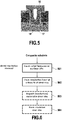
- Fig.5 is a diagram representing, in an enlarged view, an example of a blind via 15 that may be used in the interposer of Fig.4 .
- a layer 16 is formed at the sidewalls of the blind via-hole, and the interior of the blind via-hole is partially filled by a filling layer 17.
- a cap layer 18 is provided to ensure electrical insulation of the sidewall layer 16 (and of the filling layer 17 if it is conductive) from upper layers that may be formed on the interposer.
- the cap layer 18 is not essential.
- the blind via-hole 15 is completely filled with material so as to prevent moisture, residues or other foreign material from entering the blind via-hole 15.
- the layer 16 formed at the sidewalls of the via is an electrically-conductive layer which serves to conduct current between the grounding pattern 11 on the first surface 10c of the interposer substrate and the low-resistivity portion 10b of that substrate.
- the layer 16 may consist of doped semiconductor material. In the latter case, the layer 16 on the via sidewalls has the same dopant polarity as the low-resistivity portion 10b of the interposer substrate.
- the polarity of the dopant in the layer 16 may be the same as, or opposite to, the polarity of dopants in the high-resistivity portion 10 of the interposer substrate.
- the layer 16 is a few microns thick (up to about 3 ⁇ m thick), and has a resistivity up to about 10 ⁇ /sq. In certain preferred embodiments the resistivity of the layer 16 is around 5 ⁇ /sq.
- a common doping process may be used to dope the sidewalls of the blind via-hole to form the layer 16 and to dope an electrode layer of the 3D capacitor(s), thus avoiding the need for a specific additional step to achieve the desired doping to form the layer 16.
- the material 17 partially filling the via 15 is a layer of electrically-conductive material which can help to promote conduction of current between the grounding pattern 11 on the first surface 10c of the interposer substrate and the low-resistivity portion 10b of the substrate.
- the material 17 may be formed of various materials, for example doped semiconductor material.
- Doped polysilicon may be used to constitute the material 17. Such doped polysilicon can contribute to electrical conduction through the via 15 at high frequencies.
- the cap layer 18 (if present) may be formed of an insulating material, for example SiO 2 .
- a common doping process may be used to deposit and dope the filling material layer 17 as to deposit and dope a polysilicon electrode layer of the 3D capacitor(s), avoiding the need for specific additional steps to achieve the deposition and desired doping of the layer 17.
- Fig.6 is a flow diagram setting out a sequence of processes in an example method of fabricating an interposer according to certain embodiments of the invention.
- a composite substrate comprising a high-resistivity portion 10a and a low-resistivity portion 10b is available. If desired, the composite substrate can be made from scratch using known techniques.
- relief features are formed in the first surface 10c of the interposer substrate by any suitable process (S61).
- Various methods may be used to implement the process S61 including, but not limited to, standard deep reactive ion etching (DRIE).
- DRIE deep reactive ion etching
- This process S61 forms the blind via-holes through the high-resistivity portion 10a of the substrate.
- This process S61 may also form other desired relief features, for example relief features in/over which 3D capacitors or other components will be formed in the surface 10c of the interposer substrate.
- a process (S62) is performed to form a conductive layer at the sidewalls of the blind vias.
- Various methods may be used to implement the process S62 including, but not limited to, standard doping methods to dope the side-walls of the blind via(s) 15 (e.g. dopant diffusion at high temperature and low pressure).
- This process S62 forms a doped sidewall layer and this may constitute layer 16 shown in Fig.5 .
- This process S62 may also serve to dope sidewalls or layers in/over other relief features, such as holes, trenches or pillars in/over which 3D capacitors or other components will be formed in the surface 10c of the interposer substrate.
- a conductive material may be provided (S63) in the vias 15 by any convenient process.
- a doped polysilicon material may be deposited in the vias 15, and this may constitute filling material 17 illustrated in Fig.5 .
- an electrically-insulating layer 17 may be formed over the blind via-hole 15, for example by a low-pressure deposition process.
- this cap layer 17 helps to prevent moisture or other foreign material from entering any space remaining in the blind vias 15.
- the method for providing top-to-bottom connection through the interposer substrate consists of simple process steps that in many cases can be shared, that is, common process steps may contribute not only to formation of the top-to-bottom connection but also contribute to the fabrication of other components (e.g. 3D capacitors) desired at the first surface 10c of the substrate.
Landscapes
- Physics & Mathematics (AREA)
- Condensed Matter Physics & Semiconductors (AREA)
- General Physics & Mathematics (AREA)
- Electromagnetism (AREA)
- Optics & Photonics (AREA)
- Internal Circuitry In Semiconductor Integrated Circuit Devices (AREA)
- Engineering & Computer Science (AREA)
- Microelectronics & Electronic Packaging (AREA)
Abstract
Description
- The present invention relates to the field of interposers as well as to methods of fabricating interposers and a technique for achieving electrical interconnection through an interposer.
- Various types of interposers are used in the field of electronics. For example, optical interposers (photonic interposers) are in wide-spread use, for example as part of optical interconnects used in data centres. An optical interposer generally includes a substrate that is mounted on a mounting substrate, and elements such as a transmission line are provided on a surface of the interposer substrate that is remote from the mounting substrate. To assure desired properties for the transmission line, the interposer substrate generally is configured as an electrical insulator or is a substrate (e.g. high-resistivity (HR) silicon) having sufficiently high resistivity to prevent undesired current leakage.
- Often optical interposers are used in sets arranged side by side on a mounting substrate. For instance, a transmitter optical sub-assembly (TOSA) in a transceiver module may include four optical interposers disposed side by side. An example of such a TOSA is illustrated in
Fig.1 . - It has been found that, at high frequencies, there are peaks in the insertion loss of TOSAs, attributable to bad ground uniformity over the surface of the optical interposers.
Fig.2 illustrates how insertion loss varies with frequency in the TOSA illustrated inFig.1 . It can be seen fromFig.2 that there are insertion loss peaks at the frequency positions indicated by the arrows A. Up to now it has been considered that this problem should be addressed by improving grounding in the interposers, for example by providing wire bonds between the grounding patterns of neighbouring interposers, or wire bonds between the grounding pattern of an interposer and a grounding pattern on the underlying mounting substrate.Fig.3 is a schematic representation of an individual interposer having wire bonds connecting a grounding pattern on the interposer to ground on the mounting substrate. - However, in the case where wire bonds are used to connect a grounding pattern on the interposer to ground on the substrate or ground on neighbouring interposers, cross-talk may be generated between the bonding wires themselves.
- Besides, the impedance of these wire bonds is non-negligible. To realize an optimized ground return, its impedance and particularly the inductive behaviour of the wire bonds (correlated to the ratio length/section) can be decreased by reducing their length. From an integration point of view, this is more efficient than increasing the section of the ground return path.
- Moreover, from a purely practical point of view, appreciable space is needed to accommodate the bonding wires, which increases the footprint required for the interposer on the mounting substrate. Moreover, in some designs there is insufficient space between interposers in a group, to accommodate such bonding wires, or insufficient space between an outermost interposer and the wall of a package in which the interposer is located to allow for bonding wires to pass towards the mounting substrate.
- In principle it could be contemplated to achieve grounding between a grounding pattern on the interposer and a grounding pattern on an underlying mounting substrate by using through-silicon vias (TSVs). However, in the case of optical interposers the thickness of the interposer is relatively large (>500µm)) in order to achieve necessary optical alignment of the laser, and this would necessitate use of a long TSV. For manufacturing reasons, there are limitations on the allowable aspect ratio of a TSV and so, if the TSV is long, then the footprint occupied on the circuit board (i.e. the cross-sectional surface area of the TSV) would be large and this is incompatible with achieving a high degree of integration. Besides, TSVs are generally filled with metals that have a coefficient of thermal expansion which is quite different from the coefficient of thermal expansion of the interposer substrate, leading to undesired stresses in the interposer substrate. Furthermore, specific manufacturing steps are required in order to define, form and fill TSVs, additional to the manufacturing steps required to create the interposer and the circuit elements thereon. Thus, use of TSVs for grounding can lead to increased complexity in the manufacturing process.
- Another technique that could be contemplated to achieve grounding between a grounding pattern on the interposer and a grounding pattern on an underlying mounting substrate would be to metallize the sides of the interposer substrate. However, such an approach would likewise require additional manufacturing steps, leading to an increase in the cost and complexity of the process of manufacturing the interposer.
- The present invention has been made in the light of the above-described issues.
- The present invention provides an interposer comprising:
- a substrate; and
- a conductive pattern on a first surface of the substrate;
- characterized in that:
- the substrate is a composite substrate comprising a high-resistivity portion extending from said first surface into the bulk of the substrate, and a low-resistivity portion extending from the high-resistivity portion to a second surface of the substrate opposite to the first surface;
- at least one blind via-hole extends from said first surface of the substrate through the high-resistivity portion of the substrate into the low-resistivity portion of the substrate; and
- electrically-conductive structure is provided in the blind via-hole(s) and interconnects the conductive pattern on the first surface of the substrate with the low resistivity portion of the substrate.
- This electrically-conductive structure may be composed of a simple electrically-conductive layer provided at the sidewall of the blind via-hole but the invention is not limited to this case. For example, a multi-layer may be provided at the sidewall, this multi-layer comprising a highly-resistive material on its outer periphery overlaid with one, or several, layers having different conductivities (closer to the axis of the via-hole).
- In the case of a co-integration of the via with an adjacent capacitor, the conductive layer may comprise a stacked combination of conductive and insulating layers following the implementation of a MIM structure of the adjacent capacitor. In this case, a common set of process steps can be used to form the capacitor MIM structure and the electrically-conductive structure in the blind via-hole, thus avoiding increase in the complexity and cost of the manufacturing process.
- The high-resistivity portion of the composite substrate used in the above-described interposer prevents current leakage between elements (e.g. a transmission line) formed on the first surface of the interposer and the mounting substrate upon which the interposer is mounted in use. At the same time, the low-resistivity portion of the composite substrate used in the above-described interposer cooperates with conductive material in the blind via-hole(s) to establish a top-to-bottom connection structure through the interposer substrate.
- The present invention finds application not only for the purposes of establishing a grounding path through an interposer but also for other purposes. Thus, for example, the techniques of the present invention may usefully be applied in cases where it is desired to build high Q inductances on the same interposer, in cases where it is desired to manage electrically-independent GND domains on a common interposer, etc.
- With the above-described structure, an interposer according to embodiments of the invention can establish a direct conductive path, for example between the interposer grounding pattern (die ground) and the ground of a mounting substrate upon which the interposer is mounted in use, through the die itself. This shortens the length of the electrical connection. Accordingly, in the case of using the through-interposer connection for grounding, the length of the ground connection between the interposer and the mounting substrate is reduced, and the uniformity of the ground potential is increased.
- The above-described interposer structure enables grounding to be achieved without using bonding wires for this purpose. Accordingly, no extra footprint on the mounting substrate is required. The above-described interposer structure enables grounding to be achieved without using TSVs for this purpose, reducing the complexity of the manufacturing process (see below). Similar advantages arise in the case where the through-interposer connection is used for connecting a pattern on the interposer which is not a grounding pattern to a conductor on the mounting substrate.
- In the above-described interposer, the electrically-conductive material in the blind via-hole(s) may comprise a conductive layer provided on the side walls of the blind via-hole(s). The low-resistivity portion of the substrate, and the conductive layer provided on the side wall of the blind via-hole(s), may both be made of semiconductor material and may be doped by dopants of the same polarity as one another. The high-resistivity portion of the interposer substrate may also be made of semiconductor and may have doping of the same or different polarity from that of the doped via-hole sidewalls.
- In the above-described interposer, a filling may be provided in the blind via-holes to prevent ingress of undesired impurities and the like. In some cases, a doped polysilicon filling material may be provided in the blind via-hole(s) and this acts as an additional contributor for top-to-bottom connection through the interposer. In some cases the interposer contains 3D capacitors (e.g. trench capacitors) as well as the blind via-holes, and during formation of the dielectric and electrode layers of the 3D capacitors the same dielectric and conductive materials may be deposited into the blind via-holes such that insulating layers are deposited within the via between the doped walls and the polysilicon itself, thus creating an auxiliary capacitor. At high frequencies, the impedance of this auxiliary capacitor becomes negligible and current can flow from the polysilicon to the low-resistivity portion of the substrate, in addition to the main parallel path formed by the conductive side walls of the blind via-hole. This improves the high-frequency performance of the device, and reduces electrical losses.
- Certain embodiments of interposer according to the invention have a transmission line provided on the first surface of the substrate and the high-resistivity portion of the substrate impedes current leakage, or losses, from the transmission line to the high-resistivity portion of the substrate (and, therefore, impedes current leakage to the mounting substrate).
- The present invention further provides a method of fabricating an interposer, comprising:
- forming relief features in a first surface of a composite substrate, said composite substrate comprising a high-resistivity portion extending from said first surface into the bulk of the substrate, and a low-resistivity portion extending from the high-resistivity portion to a second surface of the substrate opposite to the first surface, and said relief features comprising a set of blind via-holes extending from said first surface of the substrate through the high-resistivity portion of the substrate into the low-resistivity portion of the substrate; and
- forming an electrically-conductive layer at the side walls of the blind via-holes;
- whereby the conductive layer and the low-resistivity portion of the substrate form a current path through the interposer substrate.
- The above-recited method provides comparable advantages to those mentioned above in relation to the interposer. Formation of the blind via-holes in the above-described method is simpler than formation of TSVs, notably because the blind via-holes do not need to traverse the full thickness of the interposer substrate. Moreover, only a limited number of process steps are required in order to form the new structure.
- The electrically-conductive sidewall layer may be connected to a grounding pattern on the first surface of the substrate, thus providing a grounding path through the interposer.
- The above-described method may include a step of wholly or partially filling the blind via-holes with material, to prevent ingress of impurities, humidity, etc. The material wholly or partially filling the blind via-holes may be an electrically-conductive material, e.g. doped polysilicon.
- Moreover, in several types of interposer it may be necessary to form other holes in the first surface of the interposer substrate, besides the blind via-holes. In such cases, a common set of process steps may be used to form the blind via-holes and the holes required by the other components on the interposer, so that the presence of the blind via-holes causes a negligible increase in the complexity of the process of manufacturing the interposer.
- In certain example implementations, the interposer includes 3D capacitors formed in holes (e.g. trenches), or formed over pillars, at the first surface of the interposer substrate. In such cases, common process steps may be used to form the holes/pillars of the 3D capacitors and to form the blind via-holes of the invention. Furthermore, process steps which form layers of the 3D capacitor structure may be exploited to also deposit material on the side walls of, or within, the blind via-holes of the invention. Once again, the presence of the blind via-holes causes a negligible increase in the complexity of the process of manufacturing such interposers.
- Further features and advantages of the present invention will become apparent from the following description of certain embodiments thereof, given by way of illustration only, not limitation, with reference to the accompanying drawings in which:
-
Figure 1 is a drawing illustrating a transmitter optical sub-assembly (TOSA) in a transceiver module, including four optical interposers; -
Figure 2 is a graph showing how insertion loss varies with frequency in an optical interposer of the TOSA illustrated inFig.1 ; -
Figure 3 illustrates schematically an interposer according to the related art, mounted on a mounting substrate and using bonding wires for grounding; -
Figure 4 illustrates schematically an interposer according to an embodiment of the invention, mounted on a mounting substrate; -
Figure 5 illustrates schematically an example of a blind via that may be used in the interposer ofFig.3 ; and -
Figure 6 is a flow diagram illustrating the main stages in a method, according to an example embodiment of the present invention, for fabricating an interposer such as that ofFig.4 . - An interposer according to an embodiment of the invention will now be described with reference to
Figs.4 and5 , and an example manufacturing method for fabricating the interposer will be described with reference toFig.6 . In the example described with reference toFigs.4-6 , the interposer is an optical interposer and a through-interposer connection is implemented using blind via-holes and a composite substrate. However, it should be noted that the invention is not limited to application in optical interposers nor to application for through-interposer connections that realize grounding. The invention may be applied more generally in interposers of substantially any type in order to implement a through-interposer electrical connection. - As can be seen from
Fig.4 , an example interposer 1 according to an embodiment of the invention includes asubstrate 10 which is a composite substrate consisting of first andsecond portions first surface 10c of the interposer (positioned at the top of the interposer in the orientation illustrated inFig.4 ) into the bulk of the substrate. The second portion, 10b, of the interposer substrate is a low-resistivity portion extending from the high-resistivity portion 10a to asecond surface 10d of the interposer (positioned at the bottom of the interposer in the orientation illustrated inFig.4 ) opposite to thefirst surface 10c. Typical interposer dimensions are length of 1.5mm, width of 1 mm and thickness/height of 0.5mm. -
Fig.4 represents the interposer 1 in a state where it is mounted on a mounting substrate 2 (e.g. a printed circuit board, or other support) and connected to another component Q by bonding wires. The nature of the component Q is not germane to the invention and so this component shall not be discussed further in this document. Thefirst surface 10c of the interposer substrate faces away from the mountingsubstrate 2 and the second surface of the interposer substrate, 10d, is positioned on the mountingsubstrate 2. The interposer may be fixed to the mounting substrate in any convenient manner, for example viabackside metallization 20 as illustrated inFig.4 , by solder paste, etc. - A
grounding pattern 11 is provided on thefirst surface 10c of the interposer substrate. Thegrounding pattern 11 covers a large fraction of thefirst surface 10c of the interposer substrate. In this example atransmission line 12 is also provided on thefirst surface 10c of the interposer substrate with a gap between the periphery of thetransmission line 12 and neighbouring portions of thegrounding pattern 11. This example relates to an optical interposer 1 in which alaser 14 is also mounted on the interposer and is connected to the component Q by thetransmission line 12. The high-resistivity portion 10a of the interposer substrate prevents, or at least reduces, current leakage from thetransmission line 12 to the mountingsubstrate 2. - The thickness of the high-
resistivity portion 10a of the substrate is set dependent on the total thickness and permittivity of the interposer, as well as on the dimensions (width and gap) of the transmission line permittivity. In particular, the thickness of the high-resistivity portion 10a is preferably set sufficiently large so as to achieve desired performance in terms of blocking leakage-current / reduction of electrical losses from the transmission line. In some embodiments of the invention the high-resistivity portion 10a of the interposer substrate has a thickness taking a value that can range from approximately 10µm to approximately 400µm, more preferably greater than 150µm, so as to reduce current leakage from thetransmission line 12 to the mountingsubstrate 2 to a minimal, or tolerable, amount. A typical thickness value for the high-resistivity portion 10a is 200µm. - The invention is not particularly concerned with the transmission line and laser used in example embodiments such as that illustrated in
Fig.4 and, accordingly, no further details of those components will be given here. - In the interposer illustrated in
Fig.4 , a plurality of blind via-holes 15 extend from thefirst surface 10c of the interposer substrate, through the high-resistivity portion 10a of the substrate and into the low-resistivity portion 10b of the substrate where they finish still some distance away from thesecond surface 10d of the interposer substrate. Electrically conductive material (seeFig.5 ) is provided on the sidewalls of the blind via-holes and/or as a filling that completely or partially fills the via-holes. A top-to-bottom connection is established between the groundingpattern 11 on the first surface of the interposer substrate and a grounding pattern (not shown) provided on the mountingsubstrate 2 via the electrically-conductive material in the blind via-holes 15 and via the low-resistivity portion 10b of the interposer substrate. This connection is established in a space-saving manner within the existing footprint of theinterposer substrate 10 on the mountingsubstrate 2. - In the context illustrated in
Fig.4 , where the through-interposer connection serves for grounding in an optical interposer, it is desirable for the number and dimensions of the blind via-holes to be set with a view to achieving a target value for the impedance of thecoplanar ground plane 11 relative to the characteristic impedance (Zcl) of the transmission line provided on the interposer. For example, the number and dimensions of the via-holes may be set with a view to making the impedance of theground plane 11 low relative to Zcl. For example, the target impedance value for thecoplanar ground plane 11 may be set at less than 10% of Zcl. So, for instance, if the transmission line's characteristic impedance is 50 Ohm then the impedance of its coplanar ground plane may be set at < 5 ohms by controlling the properties of the blind via-holes. The impedance of one via will depend on its chosen dimensions. The minimum number of vias will depend on the necessary number to reach the target impedance for thegrounding pattern 11. - The thickness of the low-
resistivity portion 10b of the substrate may be set to achieve a target thickness of the overall interposer, for a given thickness of the high-resistivity portion 10a, with a view to keeping the length of the through-interposer connection short. So, for instance, in the example illustrated inFig.4 , there is a certain overall height of the interposer (c. 500µm) that typically is required in view of proper optical alignment of the laser with a neighbouring component. Accordingly, it may be appropriate to determine a target overall thickness Tint of the interposer, a target thickness THR of the high-resistivity portion 10a of the substrate (in view of adequate prevention of current leakage/reduction in losses) and then to set the thickness TLR of the low-resistivity portion 10b to TLR = Tint- THR. In most applications, the thickness of the low-resistivity portion 10b of the interposer substrate is in the range from approximately 1µm to 1mm so as to keep the length of the ground connection short. - In the interposer illustrated in
Fig.4 , the interposer substrate may be made of various different materials. It is convenient to make thesubstrate 10 of a semiconductor material, e.g. silicon, in view of the highly-developed state of manufacturing processes that have been designed to process silicon wafers. Indeed, composite silicon substrates having low-resistivity and high-resistivity layers are known for use in other applications and may be procured for use in making interposers according to embodiments of the invention. However, the invention is not limited to the use of silicon substrates; other substrate materials (notably semiconducting materials) may be used, e.g. GaAs, InP, GaN, InAs, etc. - In preferred embodiments, the high-
resistivity portion 10a of the interposer substrate may have a resistivity value ≥ 100 Ω.cm, and more preferably of ≥ 1 kΩ.cm. In preferred embodiments, the low-resistivity portion 10b of the interposer substrate may have a resistivity value that is no more than 1 Ω.cm, and more preferably that is less than 10 mΩ.cm. Typically, in order to achieve the desired difference between their resistivity values, high-resistivity and low-resistivity portions resistivity portion 10a of the substrate is p-- doped silicon, for example doped with boron, whereas the low-resistivity portion 10b of the substrate is n++ doped, for example doped with As, P or Sb. -
Fig.5 is a diagram representing, in an enlarged view, an example of a blind via 15 that may be used in the interposer ofFig.4 . - In the example illustrated in
Fig.5 , alayer 16 is formed at the sidewalls of the blind via-hole, and the interior of the blind via-hole is partially filled by afilling layer 17. Acap layer 18 is provided to ensure electrical insulation of the sidewall layer 16 (and of thefilling layer 17 if it is conductive) from upper layers that may be formed on the interposer. Thecap layer 18 is not essential. In many cases the blind via-hole 15 is completely filled with material so as to prevent moisture, residues or other foreign material from entering the blind via-hole 15. - The
layer 16 formed at the sidewalls of the via is an electrically-conductive layer which serves to conduct current between the groundingpattern 11 on thefirst surface 10c of the interposer substrate and the low-resistivity portion 10b of that substrate. Thelayer 16 may consist of doped semiconductor material. In the latter case, thelayer 16 on the via sidewalls has the same dopant polarity as the low-resistivity portion 10b of the interposer substrate. The polarity of the dopant in thelayer 16 may be the same as, or opposite to, the polarity of dopants in the high-resistivity portion 10 of the interposer substrate. Typically, thelayer 16 is a few microns thick (up to about 3µm thick), and has a resistivity up to about 10 Ω/sq. In certain preferred embodiments the resistivity of thelayer 16 is around 5 Ω/sq. - In a case where one or more 3D capacitors is/are also formed in the
first surface 10c of the interposer substrate, a common doping process may be used to dope the sidewalls of the blind via-hole to form thelayer 16 and to dope an electrode layer of the 3D capacitor(s), thus avoiding the need for a specific additional step to achieve the desired doping to form thelayer 16. - In some embodiments, the
material 17 partially filling the via 15 is a layer of electrically-conductive material which can help to promote conduction of current between the groundingpattern 11 on thefirst surface 10c of the interposer substrate and the low-resistivity portion 10b of the substrate. In such a case, thematerial 17 may be formed of various materials, for example doped semiconductor material. - Doped polysilicon may be used to constitute the
material 17. Such doped polysilicon can contribute to electrical conduction through the via 15 at high frequencies. - The cap layer 18 (if present) may be formed of an insulating material, for example SiO2.
- In a case where one or more 3D capacitors is/are also formed in the
first surface 10c of the interposer substrate, a common doping process may be used to deposit and dope the fillingmaterial layer 17 as to deposit and dope a polysilicon electrode layer of the 3D capacitor(s), avoiding the need for specific additional steps to achieve the deposition and desired doping of thelayer 17. -
Fig.6 is a flow diagram setting out a sequence of processes in an example method of fabricating an interposer according to certain embodiments of the invention. In the method illustrated inFig.6 , it is assumed that a composite substrate comprising a high-resistivity portion 10a and a low-resistivity portion 10b is available. If desired, the composite substrate can be made from scratch using known techniques. - In the example method of
Fig.6 , relief features (holes, pillars, trenches) are formed in thefirst surface 10c of the interposer substrate by any suitable process (S61). Various methods may be used to implement the process S61 including, but not limited to, standard deep reactive ion etching (DRIE). This process S61 forms the blind via-holes through the high-resistivity portion 10a of the substrate. This process S61 may also form other desired relief features, for example relief features in/over which 3D capacitors or other components will be formed in thesurface 10c of the interposer substrate. - Next, a process (S62) is performed to form a conductive layer at the sidewalls of the blind vias. Various methods may be used to implement the process S62 including, but not limited to, standard doping methods to dope the side-walls of the blind via(s) 15 (e.g. dopant diffusion at high temperature and low pressure). This process S62 forms a doped sidewall layer and this may constitute
layer 16 shown inFig.5 . This process S62 may also serve to dope sidewalls or layers in/over other relief features, such as holes, trenches or pillars in/over which 3D capacitors or other components will be formed in thesurface 10c of the interposer substrate. - If desired, a conductive material may be provided (S63) in the
vias 15 by any convenient process. For example, a doped polysilicon material may be deposited in thevias 15, and this may constitute fillingmaterial 17 illustrated inFig.5 . - Optionally, in a case where upper layers are going to be formed on the interposer, e.g. in relation to formation of other circuit elements of the interposer, an electrically-insulating
layer 17 may be formed over the blind via-hole 15, for example by a low-pressure deposition process. In a case where the where the blind via-holes are not completely filled, thiscap layer 17 helps to prevent moisture or other foreign material from entering any space remaining in theblind vias 15. - In the above-described example, the method for providing top-to-bottom connection through the interposer substrate consists of simple process steps that in many cases can be shared, that is, common process steps may contribute not only to formation of the top-to-bottom connection but also contribute to the fabrication of other components (e.g. 3D capacitors) desired at the
first surface 10c of the substrate. - Although the present invention has been described above with reference to certain specific embodiments, it will be understood that the invention is not limited by the particularities of the specific embodiments. Numerous variations, modifications and developments may be made in the specified embodiments within the scope of the appended claims.
Claims (12)
- An interposer (1) comprising:a substrate (10); anda conductive pattern (11) on a first surface (10c) of the substrate;characterized in that:the substrate is a composite substrate comprising a high-resistivity portion (10a) extending from said first surface (10c) into the bulk of the substrate, and a low-resistivity portion (10b) extending from the high-resistivity portion to a second surface (10d) of the substrate opposite to the first surface;a set of blind via-holes (15) extends from said first surface (10c) of the substrate through the high-resistivity portion (10a) of the substrate into the low-resistivity portion (10b) of the substrate; andelectrically-conductive material (16) is provided in the blind via-hole(s) (15) and interconnects the conductive pattern (11) on the first surface (10c) of the substrate with the low resistivity portion (10b) of the substrate.
- An interposer according to claim 1, wherein the electrically-conductive material in the blind via-hole (15) comprises a conductive layer (16) provided on the side wall of the blind via-hole.
- An interposer according to claim 2, wherein the low-resistivity portion (10b) of the substrate, and the conductive layer (16) provided on the side wall of the blind via-hole, are both made of semiconductor material and are doped by dopants of the same polarity as one another.
- An interposer according to claim 2 or 3, wherein the high-resistivity portion (10a) of the substrate, and the conductive layer (16) provided on the side wall of the blind via-hole, are both made of semiconductor material and are doped by dopants of the same polarity or opposite polarity from one another.
- An interposer according to any one of claims 1 to 4, wherein the electrically-conductive material in the blind via-hole (15) comprises a doped polysilicon filling material (17).
- An interposer according to any one of claims 1 to 5, wherein a transmission line (12) is provided on the first surface (10c) of the substrate and the high-resistivity portion (10a) of the substrate impedes current leakage from the transmission line (12) to the high-resistivity portion (10b) of the substrate.
- An interposer according to any one of claims 1 to 6, wherein the conductive pattern (11) on the first surface (10c) of the substrate is a grounding pattern.
- A method of fabricating an interposer, comprising:forming relief features in a first surface (10c) of a composite substrate (10), said composite substrate (10) comprising a high-resistivity portion (10a) extending from said first surface (10c) into the bulk of the substrate, and a low-resistivity portion (10b) extending from the high-resistivity portion to a second surface (10d) of the substrate opposite to the first surface, and said relief features comprising a set of blind via-holes (15) extending from said first surface (10c) of the substrate through the high-resistivity portion (10a) of the substrate into the low-resistivity portion (10b) of the substrate; andforming an electrically-conductive layer (16) at the side walls of the blind via-holes (15);whereby the conductive sidewall layer (16) and the low-resistivity portion (10b) of the substrate form a current path through the interposer substrate (10).
- The interposer-fabricating method according to claim 8, and comprising the step of wholly or partially filling the blind via-holes with an electrically-conductive material (17).
- The interposer-fabricating method according to claim 9, wherein the electrically-conductive material (17) wholly or partially filing the blind via-holes is doped polysilicon.
- The interposer-fabricating method according to any one of claims 8 to 10, wherein the conductive sidewall layer (16) is connected to a grounding pattern (11) on the first surface (10c) of the substrate.
- The interposer-fabricating method according to any one of claims 8 to 11, comprising steps to form one or more additional components at the first surface (10c) of the substrate, wherein one or more of the steps to form the additional component(s) is shared with a process step that forms an element contributing to said current path through the interposer.
Priority Applications (4)
| Application Number | Priority Date | Filing Date | Title |
|---|---|---|---|
| EP20305044.8A EP3855483B1 (en) | 2020-01-21 | 2020-01-21 | Through-interposer connections using blind vias |
| TW110102112A TWI888474B (en) | 2020-01-21 | 2021-01-20 | Interposer and method of fabricating said interposer |
| PCT/IB2021/050456 WO2021148977A1 (en) | 2020-01-21 | 2021-01-21 | Through-interposer grounding using blind vias |
| US17/850,495 US12400921B2 (en) | 2020-01-21 | 2022-06-27 | Through-interposer grounding using blind vias |
Applications Claiming Priority (1)
| Application Number | Priority Date | Filing Date | Title |
|---|---|---|---|
| EP20305044.8A EP3855483B1 (en) | 2020-01-21 | 2020-01-21 | Through-interposer connections using blind vias |
Publications (2)
| Publication Number | Publication Date |
|---|---|
| EP3855483A1 true EP3855483A1 (en) | 2021-07-28 |
| EP3855483B1 EP3855483B1 (en) | 2026-04-29 |
Family
ID=69423262
Family Applications (1)
| Application Number | Title | Priority Date | Filing Date |
|---|---|---|---|
| EP20305044.8A Active EP3855483B1 (en) | 2020-01-21 | 2020-01-21 | Through-interposer connections using blind vias |
Country Status (4)
| Country | Link |
|---|---|
| US (1) | US12400921B2 (en) |
| EP (1) | EP3855483B1 (en) |
| TW (1) | TWI888474B (en) |
| WO (1) | WO2021148977A1 (en) |
Citations (4)
| Publication number | Priority date | Publication date | Assignee | Title |
|---|---|---|---|---|
| EP2445004A1 (en) * | 2009-06-17 | 2012-04-25 | Hamamatsu Photonics K.K. | Laminated wiring board |
| DE102011088581A1 (en) * | 2011-03-21 | 2012-09-27 | Globalfoundries Singapore Pte. Ltd. | housing connections |
| DE102013208816A1 (en) * | 2013-05-14 | 2014-11-20 | Robert Bosch Gmbh | A method of creating a via in a CMOS substrate |
| US20150346442A1 (en) * | 2014-05-28 | 2015-12-03 | Hitachi Metals, Ltd. | Optical Communication Module and Method for Producing the Same |
Family Cites Families (7)
| Publication number | Priority date | Publication date | Assignee | Title |
|---|---|---|---|---|
| US4933739A (en) * | 1988-04-26 | 1990-06-12 | Eliyahou Harari | Trench resistor structures for compact semiconductor memory and logic devices |
| JP3241019B2 (en) * | 1999-03-15 | 2001-12-25 | 日本電気株式会社 | Coplanar railway track |
| US6847527B2 (en) * | 2001-08-24 | 2005-01-25 | 3M Innovative Properties Company | Interconnect module with reduced power distribution impedance |
| US20080012087A1 (en) * | 2006-04-19 | 2008-01-17 | Henri Dautet | Bonded wafer avalanche photodiode and method for manufacturing same |
| US8598713B2 (en) * | 2009-07-22 | 2013-12-03 | Newport Fab, Llc | Deep silicon via for grounding of circuits and devices, emitter ballasting and isolation |
| JP2011216957A (en) * | 2010-03-31 | 2011-10-27 | Furukawa Electric Co Ltd:The | High-frequency circuit board |
| CN210579552U (en) | 2017-01-27 | 2020-05-19 | 株式会社村田制作所 | Multilayer substrate and electronic device |
-
2020
- 2020-01-21 EP EP20305044.8A patent/EP3855483B1/en active Active
-
2021
- 2021-01-20 TW TW110102112A patent/TWI888474B/en active
- 2021-01-21 WO PCT/IB2021/050456 patent/WO2021148977A1/en not_active Ceased
-
2022
- 2022-06-27 US US17/850,495 patent/US12400921B2/en active Active
Patent Citations (4)
| Publication number | Priority date | Publication date | Assignee | Title |
|---|---|---|---|---|
| EP2445004A1 (en) * | 2009-06-17 | 2012-04-25 | Hamamatsu Photonics K.K. | Laminated wiring board |
| DE102011088581A1 (en) * | 2011-03-21 | 2012-09-27 | Globalfoundries Singapore Pte. Ltd. | housing connections |
| DE102013208816A1 (en) * | 2013-05-14 | 2014-11-20 | Robert Bosch Gmbh | A method of creating a via in a CMOS substrate |
| US20150346442A1 (en) * | 2014-05-28 | 2015-12-03 | Hitachi Metals, Ltd. | Optical Communication Module and Method for Producing the Same |
Also Published As
| Publication number | Publication date |
|---|---|
| US20220338349A1 (en) | 2022-10-20 |
| TWI888474B (en) | 2025-07-01 |
| WO2021148977A1 (en) | 2021-07-29 |
| US12400921B2 (en) | 2025-08-26 |
| TW202147531A (en) | 2021-12-16 |
| EP3855483B1 (en) | 2026-04-29 |
Similar Documents
| Publication | Publication Date | Title |
|---|---|---|
| US7842610B2 (en) | Semiconductor device | |
| US7099139B2 (en) | Integrated circuit package substrate having a thin film capacitor structure | |
| US7233061B1 (en) | Interposer for impedance matching | |
| KR100411870B1 (en) | A via structure | |
| US6875921B1 (en) | Capacitive interposer | |
| KR100438163B1 (en) | Semiconductor Device And Method For Fabricating The Device | |
| KR20190092584A (en) | Bonded structure with integrated passive components | |
| KR100526445B1 (en) | Wafer passivation structure | |
| US20020191380A1 (en) | Method and device for interconnecting, electronic components in three dimensions | |
| US20080291603A1 (en) | Trench Capacitor Device Suitable for Decoupling Applications in High-Frequency Operation | |
| CN1342330A (en) | Method for forming co-axial interconnect in CMOS process | |
| US12347781B2 (en) | Semiconductor devices having penetration vias | |
| CN100365798C (en) | Electronic device, assembly and method of manufacturing an electronic device | |
| US20250191847A1 (en) | Electronic device with differential transmission lines equipped with capacitors supported by a base, and corresponding manufacturing method | |
| US7525189B2 (en) | Semiconductor device, wiring board, and manufacturing method thereof | |
| US7105910B2 (en) | Semiconductor device having SOI construction | |
| CN117296159A (en) | Embeddable semiconductor-based capacitors | |
| CN117321774A (en) | Embeddable semiconductor-based capacitors | |
| US12400921B2 (en) | Through-interposer grounding using blind vias | |
| US20030071272A1 (en) | Topside active optical device apparatus and method | |
| US7911026B2 (en) | Chip carrier with reduced interference signal sensitivity | |
| US20220319958A1 (en) | Semiconductor structure, manufacturing method of semiconductor structure and stacked structure | |
| US12520595B2 (en) | Electronic device with differential transmission lines equipped with capacitors separated by a cavity, and corresponding manufacturing method | |
| EP1025570A2 (en) | Method for arrangement of a buried capacitor, and a buried capacitor arranged according to said method | |
| US20260040993A1 (en) | Electronic chips |
Legal Events
| Date | Code | Title | Description |
|---|---|---|---|
| PUAI | Public reference made under article 153(3) epc to a published international application that has entered the european phase |
Free format text: ORIGINAL CODE: 0009012 |
|
| STAA | Information on the status of an ep patent application or granted ep patent |
Free format text: STATUS: THE APPLICATION HAS BEEN PUBLISHED |
|
| AK | Designated contracting states |
Kind code of ref document: A1 Designated state(s): AL AT BE BG CH CY CZ DE DK EE ES FI FR GB GR HR HU IE IS IT LI LT LU LV MC MK MT NL NO PL PT RO RS SE SI SK SM TR |
|
| STAA | Information on the status of an ep patent application or granted ep patent |
Free format text: STATUS: REQUEST FOR EXAMINATION WAS MADE |
|
| 17P | Request for examination filed |
Effective date: 20220125 |
|
| RBV | Designated contracting states (corrected) |
Designated state(s): AL AT BE BG CH CY CZ DE DK EE ES FI FR GB GR HR HU IE IS IT LI LT LU LV MC MK MT NL NO PL PT RO RS SE SI SK SM TR |
|
| GRAP | Despatch of communication of intention to grant a patent |
Free format text: ORIGINAL CODE: EPIDOSNIGR1 |
|
| STAA | Information on the status of an ep patent application or granted ep patent |
Free format text: STATUS: GRANT OF PATENT IS INTENDED |
|
| INTG | Intention to grant announced |
Effective date: 20260102 |
|
| RIN1 | Information on inventor provided before grant (corrected) |
Inventor name: BOUVIER, STEPHANE Inventor name: LEFEUVRE, EMMANUEL Inventor name: VOIRON, FREDERIC |
|
| GRAS | Grant fee paid |
Free format text: ORIGINAL CODE: EPIDOSNIGR3 |
|
| GRAA | (expected) grant |
Free format text: ORIGINAL CODE: 0009210 |
|
| STAA | Information on the status of an ep patent application or granted ep patent |
Free format text: STATUS: THE PATENT HAS BEEN GRANTED |
|
| AK | Designated contracting states |
Kind code of ref document: B1 Designated state(s): AL AT BE BG CH CY CZ DE DK EE ES FI FR GB GR HR HU IE IS IT LI LT LU LV MC MK MT NL NO PL PT RO RS SE SI SK SM TR |
|
| REG | Reference to a national code |
Ref country code: CH Ref legal event code: F10 Free format text: ST27 STATUS EVENT CODE: U-0-0-F10-F00 (AS PROVIDED BY THE NATIONAL OFFICE) Effective date: 20260429 |