EP3851869A1 - Radar system - Google Patents
Radar system Download PDFInfo
- Publication number
- EP3851869A1 EP3851869A1 EP20152111.9A EP20152111A EP3851869A1 EP 3851869 A1 EP3851869 A1 EP 3851869A1 EP 20152111 A EP20152111 A EP 20152111A EP 3851869 A1 EP3851869 A1 EP 3851869A1
- Authority
- EP
- European Patent Office
- Prior art keywords
- signal
- frequency
- radar
- radar system
- monitoring
- Prior art date
- Legal status (The legal status is an assumption and is not a legal conclusion. Google has not performed a legal analysis and makes no representation as to the accuracy of the status listed.)
- Granted
Links
Images



Classifications
-
- G—PHYSICS
- G01—MEASURING; TESTING
- G01S—RADIO DIRECTION-FINDING; RADIO NAVIGATION; DETERMINING DISTANCE OR VELOCITY BY USE OF RADIO WAVES; LOCATING OR PRESENCE-DETECTING BY USE OF THE REFLECTION OR RERADIATION OF RADIO WAVES; ANALOGOUS ARRANGEMENTS USING OTHER WAVES
- G01S7/00—Details of systems according to groups G01S13/00, G01S15/00, G01S17/00
- G01S7/02—Details of systems according to groups G01S13/00, G01S15/00, G01S17/00 of systems according to group G01S13/00
- G01S7/40—Means for monitoring or calibrating
-
- G—PHYSICS
- G01—MEASURING; TESTING
- G01S—RADIO DIRECTION-FINDING; RADIO NAVIGATION; DETERMINING DISTANCE OR VELOCITY BY USE OF RADIO WAVES; LOCATING OR PRESENCE-DETECTING BY USE OF THE REFLECTION OR RERADIATION OF RADIO WAVES; ANALOGOUS ARRANGEMENTS USING OTHER WAVES
- G01S13/00—Systems using the reflection or reradiation of radio waves, e.g. radar systems; Analogous systems using reflection or reradiation of waves whose nature or wavelength is irrelevant or unspecified
- G01S13/87—Combinations of radar systems, e.g. primary radar and secondary radar
-
- G—PHYSICS
- G01—MEASURING; TESTING
- G01S—RADIO DIRECTION-FINDING; RADIO NAVIGATION; DETERMINING DISTANCE OR VELOCITY BY USE OF RADIO WAVES; LOCATING OR PRESENCE-DETECTING BY USE OF THE REFLECTION OR RERADIATION OF RADIO WAVES; ANALOGOUS ARRANGEMENTS USING OTHER WAVES
- G01S13/00—Systems using the reflection or reradiation of radio waves, e.g. radar systems; Analogous systems using reflection or reradiation of waves whose nature or wavelength is irrelevant or unspecified
- G01S13/02—Systems using reflection of radio waves, e.g. primary radar systems; Analogous systems
- G01S13/06—Systems determining position data of a target
- G01S13/08—Systems for measuring distance only
- G01S13/32—Systems for measuring distance only using transmission of continuous waves, whether amplitude-, frequency-, or phase-modulated, or unmodulated
- G01S13/34—Systems for measuring distance only using transmission of continuous waves, whether amplitude-, frequency-, or phase-modulated, or unmodulated using transmission of continuous, frequency-modulated waves while heterodyning the received signal, or a signal derived therefrom, with a locally-generated signal related to the contemporaneously transmitted signal
-
- G—PHYSICS
- G01—MEASURING; TESTING
- G01S—RADIO DIRECTION-FINDING; RADIO NAVIGATION; DETERMINING DISTANCE OR VELOCITY BY USE OF RADIO WAVES; LOCATING OR PRESENCE-DETECTING BY USE OF THE REFLECTION OR RERADIATION OF RADIO WAVES; ANALOGOUS ARRANGEMENTS USING OTHER WAVES
- G01S13/00—Systems using the reflection or reradiation of radio waves, e.g. radar systems; Analogous systems using reflection or reradiation of waves whose nature or wavelength is irrelevant or unspecified
- G01S13/88—Radar or analogous systems specially adapted for specific applications
- G01S13/93—Radar or analogous systems specially adapted for specific applications for anti-collision purposes
- G01S13/931—Radar or analogous systems specially adapted for specific applications for anti-collision purposes of land vehicles
-
- G—PHYSICS
- G01—MEASURING; TESTING
- G01S—RADIO DIRECTION-FINDING; RADIO NAVIGATION; DETERMINING DISTANCE OR VELOCITY BY USE OF RADIO WAVES; LOCATING OR PRESENCE-DETECTING BY USE OF THE REFLECTION OR RERADIATION OF RADIO WAVES; ANALOGOUS ARRANGEMENTS USING OTHER WAVES
- G01S7/00—Details of systems according to groups G01S13/00, G01S15/00, G01S17/00
- G01S7/02—Details of systems according to groups G01S13/00, G01S15/00, G01S17/00 of systems according to group G01S13/00
- G01S7/35—Details of non-pulse systems
- G01S7/352—Receivers
-
- G—PHYSICS
- G01—MEASURING; TESTING
- G01S—RADIO DIRECTION-FINDING; RADIO NAVIGATION; DETERMINING DISTANCE OR VELOCITY BY USE OF RADIO WAVES; LOCATING OR PRESENCE-DETECTING BY USE OF THE REFLECTION OR RERADIATION OF RADIO WAVES; ANALOGOUS ARRANGEMENTS USING OTHER WAVES
- G01S7/00—Details of systems according to groups G01S13/00, G01S15/00, G01S17/00
- G01S7/02—Details of systems according to groups G01S13/00, G01S15/00, G01S17/00 of systems according to group G01S13/00
- G01S7/40—Means for monitoring or calibrating
- G01S7/4004—Means for monitoring or calibrating of parts of a radar system
- G01S7/4017—Means for monitoring or calibrating of parts of a radar system of HF systems
-
- G—PHYSICS
- G01—MEASURING; TESTING
- G01S—RADIO DIRECTION-FINDING; RADIO NAVIGATION; DETERMINING DISTANCE OR VELOCITY BY USE OF RADIO WAVES; LOCATING OR PRESENCE-DETECTING BY USE OF THE REFLECTION OR RERADIATION OF RADIO WAVES; ANALOGOUS ARRANGEMENTS USING OTHER WAVES
- G01S7/00—Details of systems according to groups G01S13/00, G01S15/00, G01S17/00
- G01S7/02—Details of systems according to groups G01S13/00, G01S15/00, G01S17/00 of systems according to group G01S13/00
- G01S7/40—Means for monitoring or calibrating
- G01S7/4004—Means for monitoring or calibrating of parts of a radar system
- G01S7/4021—Means for monitoring or calibrating of parts of a radar system of receivers
-
- G—PHYSICS
- G01—MEASURING; TESTING
- G01S—RADIO DIRECTION-FINDING; RADIO NAVIGATION; DETERMINING DISTANCE OR VELOCITY BY USE OF RADIO WAVES; LOCATING OR PRESENCE-DETECTING BY USE OF THE REFLECTION OR RERADIATION OF RADIO WAVES; ANALOGOUS ARRANGEMENTS USING OTHER WAVES
- G01S13/00—Systems using the reflection or reradiation of radio waves, e.g. radar systems; Analogous systems using reflection or reradiation of waves whose nature or wavelength is irrelevant or unspecified
- G01S13/88—Radar or analogous systems specially adapted for specific applications
- G01S13/93—Radar or analogous systems specially adapted for specific applications for anti-collision purposes
- G01S13/931—Radar or analogous systems specially adapted for specific applications for anti-collision purposes of land vehicles
- G01S2013/9327—Sensor installation details
- G01S2013/93271—Sensor installation details in the front of the vehicles
-
- G—PHYSICS
- G01—MEASURING; TESTING
- G01S—RADIO DIRECTION-FINDING; RADIO NAVIGATION; DETERMINING DISTANCE OR VELOCITY BY USE OF RADIO WAVES; LOCATING OR PRESENCE-DETECTING BY USE OF THE REFLECTION OR RERADIATION OF RADIO WAVES; ANALOGOUS ARRANGEMENTS USING OTHER WAVES
- G01S7/00—Details of systems according to groups G01S13/00, G01S15/00, G01S17/00
- G01S7/02—Details of systems according to groups G01S13/00, G01S15/00, G01S17/00 of systems according to group G01S13/00
- G01S7/35—Details of non-pulse systems
- G01S7/352—Receivers
- G01S7/356—Receivers involving particularities of FFT processing
Definitions
- the disclosure relates to a radar system comprising multiple synchronized transceivers.
- ICs integrated circuits
- ADCs analog to digital converters
- two signals may be used, one in the range of between 40MHz to 500MHz to synchronize the PLL (phase locked loop) clock and another digital signal to synchronize the start of modulation and ADC sampling.
- the high frequency signals must also be correlated and coherent in phase.
- one master LO (local oscillator) signal may be distributed to all the chips to drive a mixer at the transmitter (TX) and at the receiver (RX).
- This signal may be in the range of between 20GHz to 40GHZ.
- This high frequency signal must be routed from the master signal generator to all the slaves with the same transmission path length in order to maintain phase alignment.
- the high frequency LO signal has to be routed in the PCB, which adds high losses to the LO signal. This may be compensated by increasing the output power at the LO transmitter in the master transceiver, which increases power consumption and power dissipation, or by limiting the number of transceivers that can be cascaded.
- the high frequency LO signal may be distributed to the slave transceivers through coaxial cables, waveguides or a wireless link.
- a radar system comprising:
- Using a lower frequency monitoring signal which may for example be in the range of 40 MHz to 240 MHz, allows phase difference and relative frequency differences to be calculated by the microcontroller unit, which can be used to compensate for phase and frequency errors during signal processing.
- the monitoring signals being at a lower frequency than the radar frequency range, can be more easily distributed without the need for specialised waveguides or substrates, allowing greater flexibility in design of a radar system. This enables both co-located and non-co-located larger cascade systems to be built.
- the low frequency clock signal may be within a range between 40 MHz and 500 MHz, for example between around 40 MHz and 60 MHz.
- the modulated high frequency signal may be within a range of between 76 GHz and 81 GHz.
- the radar system may comprise four or more radar transceiver units.
- Each of the plurality of radar transceiver units may comprise a voltage controlled oscillator, VCO, for generating the modulated high frequency signal in combination with the intermediate frequency signal.
- VCO voltage controlled oscillator
- the monitoring signal may be a digital signal comprising phase and frequency information of the modulated high frequency signal.
- each of the plurality of radar transceiver units may comprise a clock signal generator for providing the low frequency clock signal.
- a clock signal generator may be configured to provide a common low frequency clock signal to each of the plurality of radar transceiver units.
- Each of the plurality of radar transceiver units may comprise a VCO monitoring module comprising a first frequency divider configured to receive the modulated high frequency signal, a second frequency divider configured to receive the intermediate frequency signal, a mixer configured to mix outputs from the first and second frequency dividers and an analog to digital converter, ADC, configured to provide a digital monitoring signal from an output of the mixer.
- VCO monitoring module comprising a first frequency divider configured to receive the modulated high frequency signal, a second frequency divider configured to receive the intermediate frequency signal, a mixer configured to mix outputs from the first and second frequency dividers and an analog to digital converter, ADC, configured to provide a digital monitoring signal from an output of the mixer.
- microcontroller unit may be configured to:
- microcontroller unit may be configured to:
- microcontroller unit may be configured to:
- the plurality of radar transceiver units may be co-located on a common substrate, or may be located on separate substrates.
- An automotive radar system may comprise a radar system as defined and described herein.
- FIG. 1 illustrates an example conventional automotive radar system 100, comprising a radar microcontroller unit (MCU) 101 and three transceiver units 102a-c.
- Transceiver unit 102a is a master unit, and provides a VCO signal 103 to each of the two slave transceiver units 102b, 102c.
- a reference clock signal 104 is provided to each of the transceiver units 102a-c by a clock signal generator 105, which may for example operate at 40 to 60 MHz.
- a pulse signal is provided by the MCU 101 to each transceiver unit 102a-c to indicate the start of modulation, and the clock signal 104 is used to synchronize the digital clocks of the transceiver units 102a-c.
- the VCO signal 103 provided by the master transceiver unit 102a ensures synchronization of frequency and time of the high frequency signal, with the slave transceiver units 102b, 102c using only mixers and amplifiers at the transmitter and receiver paths
- VCOs of the transceivers 102a-c are instead run independently and with no synchronization, frequency and phase differences will tend to occur between the transceiver units 102a-c due to process, temperature and voltage variations across the transceiver units 102a-c, making the radar system 100 inoperable.
- FIG. 2 illustrates an example radar system 200 in accordance with the present disclosure.
- the system comprises an MCU 201, a clock signal generator 205 and a plurality of transceiver units 202a-c, the clock signal generator 205 providing a reference clock signal 204 to each of the transceiver units 202a-c.
- the clock signal generator 205 providing a reference clock signal 204 to each of the transceiver units 202a-c.
- three transceiver units 202a-c are shown, but this number is for example only. In practice the number of transceiver units may be greater than this or as few as two, although the principles described herein have advantages for a system having a greater number of units, for example four or more.
- VCO monitor signals 203a-c are provided by the respective transceiver units 202a-c to the MCU 201, each VCO monitor signal 203a-c being derived from a VCO signal generated internally by each transceiver unit 202a-c.
- Each VCO monitoring signal 203a-c is a frequency scaled version of the internal VCO signal in each transceiver unit 202a-c, the frequency being scaled by a linear factor. This enables the VCO monitoring signals 203a-c to be transported via simple low cost connections or to be digitized without loss of phase and frequency information.
- the VCO monitoring signals 203a-c are compared by the MCU 201 and the relative phase and frequency differences of the VCO signals within each transceiver unit 202a-c calculated.
- Knowledge of the relative phase and frequency differences enables compensation to be made in the digital domain by applying simple linear transformations. Such compensation may be made by convolution in the frequency domain, involving dividing the original signal over all frequencies by the error signal at a single frequency.
- the reference clock signal 204 is a low frequency signal (e.g. 40 to 60 MHz) that is used as a reference by each transceiver unit 202a-c to generate high frequency signals for transmission and reception of radar signals, which may be in the range of 76-81 GHz.
- the reference clock signal 204 may be generated by a single clock signal generator 205 as in the example of Figure 2 , thereby ensuring that there is no frequency drift between the transceivers 202a-c, or may alternatively be generated separately for each transceiver unit 202a-c, provided the frequency drift can be designed to be low. Small frequency drifts between the clock signals, for example up to around 10% of the sampling frequency of the ADC at the receiver, can be compensated for.
- the VCO monitoring signal 203a-c may be used to calculate any differences, which can be compensated for by shifting the signals in the frequency domain.
- a clock signal 204a-c is provided to each transceiver 202a-c by a respective clock signal generator 205a-c.
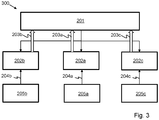
- the other components of the system 300 are the same as in the system 200 of Figure 2 .
- operation of the system 200, 300 begins with a trigger signal, for example in the form of a pulse, being sent from the MCU 201 to each transceiver unit 202a-c to synchronize the start of modulation.
- a trigger signal for example in the form of a pulse
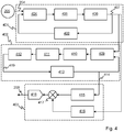
- Figure 4 illustrates first and second phase-locked loops 401, 402 and a VCO monitoring module 403, which are provided as part of an example transceiver unit.
- the first PLL 401 generates an intermediate frequency signal 407 and the second PLL generates a high frequency modulated signal 419.
- the frequency modulated signal 419 and the intermediate frequency signal are divided in frequency and are combined and digitized to provide a VCO monitoring signal 203.
- a reference clock signal 204 is provided by a clock signal generator 205 to a first phase-frequency detector (PFD) 404, which provides an output signal to a first low-pass filter 405.
- PFD phase-frequency detector
- the low-pass filtered signal is then provided to a first VCO 406, which generates an intermediate frequency (IF) signal 407.
- IF intermediate frequency
- the IF signal 407 is provided to a second PFD 409, which provides an output signal to a charge pump 410, which provides a signal to a second first low-pass filter 411.
- the low-pass filtered signal is then provided to a second VCO 412, the output of which is the VCO high frequency signal 419, within a range between 76 and 81 GHz.
- the high frequency signal 419 is fed back to the second PFD 409 via a second frequency divider 413.
- the outputs 407, 419 from the first and second PLLs 401, 402 are provided to the VCO monitoring module 403.
- the VCO monitoring module 403 comprises third and fourth frequency dividers 415, 416, to which the respective outputs 407, 414 from the first and second PLLs 401, 402 are provided.
- the outputs from the third and fourth frequency dividers 415, 416 are provided to a mixer 417, which provides an output to an ADC 418.
- the output signal 203 from the ADC provides the VCO monitoring signal to the MCU 201 for the transceiver unit.
- the frequency modulated signal 414 from the second PLL 402 may be downconverted to be digitized or may be digitized after the frequency divider.
- the second and third frequency dividers 413, 415 divide in frequency the VCO signal 419, which is then down-converted by the mixer 417.
- a digital counter may be used to count the number of zero crossings of the output signal 419 over a set period of time to calculate the frequency of the signal 419.
- the phase detector 409 at the PLL 402 may be used to calculate the relative phase of the signal 419 relative to the PLL reference signal.
- the RX channel information and the VCO monitoring signals 203a-c have to be processed in a central processing unit such as the MCU 201. If the RX data and the VCO monitoring data are digitized, the information can be merged and transported by means of a high speed communication bus using a protocol such as a camera serial interface (e.g. MIPI-CSI2), Ethernet or another type of high speed bus.
- a protocol such as a camera serial interface (e.g. MIPI-CSI2), Ethernet or another type of high speed bus.
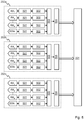
- Figure 5 illustrates an example of this using high speed communication via MIPI-CSI2.
- the VCO monitor signal 203a-c is provided in parallel with received radar data over N channels RX 1 , RX 2 to RX N in sequence to a deserializer 501 and word aligner 502. Outputs from the word aligners 502 are provided to a lane aligner 503 and then to a parser 504, the output of which is provided to the MCU 201.
- the MCU 201 calculates the frequency difference and phase difference between the VCOs in each transceiver unit 202a-c. Various methods may be used to do this, based on FFT (fast Fourier transform) processing.
- FFT fast Fourier transform
- one of the VCOs is selected as a reference (step 601) and the raw ADC samples of the reference VCO monitoring signal is multiplied with the VCO monitoring signal to be compared (step 602), simulating a mixer in the digital domain.
- the FFT of the resulting signal is calculated (step 603) and the frequency component with the highest energy close to the frequency zero determined (step 604).
- the frequency difference and phase information are then used to compensate the RX data (step 605).
- an FFT is calculated of each of the different VCO monitoring signals (step 701).
- One of the signals is selected as a reference (step 702).
- a maximum peak is determined in the magnitude of each FFT (step 703).
- a frequency difference between reference signals and the other VCOs is calculated (step 704).
- the phase is determined and subtracted from the reference VCO signal (step 705). The frequency difference and phase difference are then used to compensate on all of the RX channels (step 706).
- the instant phase for each of the VCO monitoring signals is calculated (step 801). This may be calculated by applying a Hilbert transform to the VCO monitoring signal. The phase is then calculated from the complex signal (step 802). From the derivative of the phase, the instant frequency can be calculated (step 803). One of the VCO monitoring signals is selected as a reference (step 804) and the instant frequency and phase is subtracted from the other VCO monitoring signals (step 805). The resulting values are then used to calibrate the RX channels (step 806).
- the system and methods described herein may be applied to co-located radar systems, in which a plurality of transceivers is co-located on a common PCB.
- An advantage is that there is no need to distribute a high frequency signal from a master chip to each slave chip to synchronize each transceiver, which allows the transceivers to be positioned on the PCB in a more flexible way, reducing the distance between the transceiver and the antennae.
- a further advantage is not needing to use expensive high frequency PCB substrates if the antennae are integrated into each transceiver.
- a system of the type described herein may also be implemented in a non-co-located or distributed cooperative radar system, for example in an automotive radar application.
- Figure 9 illustrates a car 900 having multiple radar sensors 901a-c mounted at different locations around a front of the car 901, with a MCU 201 connected to each of the sensors 901a-c.
- the fields of view 902a-c of the sensors 901a-c have overlapping portions 903a, 903b.
- the sensors 901a-c can be arranged as a co-operative net of sensors, resulting in an increased angular resolution as compared with a non-co-operative version.
Landscapes
- Engineering & Computer Science (AREA)
- Radar, Positioning & Navigation (AREA)
- Remote Sensing (AREA)
- Physics & Mathematics (AREA)
- Computer Networks & Wireless Communication (AREA)
- General Physics & Mathematics (AREA)
- Electromagnetism (AREA)
- Radar Systems Or Details Thereof (AREA)
Abstract
Description
- The disclosure relates to a radar system comprising multiple synchronized transceivers.
- In automotive radar applications, if more than four transmitting and receiving signals are required, multiple integrated circuits (ICs, or chips) generally need to be cascaded and synchronized. To achieve synchronization, digital clocks of all the ICs must have the same frequency and phase. This is particularly important for the clocks driving the ADCs (analog to digital converters) at the receiver. For this purpose, two signals may be used, one in the range of between 40MHz to 500MHz to synchronize the PLL (phase locked loop) clock and another digital signal to synchronize the start of modulation and ADC sampling. The high frequency signals must also be correlated and coherent in phase. For this reason, one master LO (local oscillator) signal may be distributed to all the chips to drive a mixer at the transmitter (TX) and at the receiver (RX). This signal may be in the range of between 20GHz to 40GHZ. This high frequency signal must be routed from the master signal generator to all the slaves with the same transmission path length in order to maintain phase alignment.
- When the transceivers are co-located in the same PCB (printed circuit board), the high frequency LO signal has to be routed in the PCB, which adds high losses to the LO signal. This may be compensated by increasing the output power at the LO transmitter in the master transceiver, which increases power consumption and power dissipation, or by limiting the number of transceivers that can be cascaded. In applications where the transceivers are not co-located, such as in a distributed co-operative system, the high frequency LO signal may be distributed to the slave transceivers through coaxial cables, waveguides or a wireless link. These alternatives, however, increase the complexity and cost of the radar system.
- In accordance with the present disclosure there is provided a radar system comprising:
- a plurality of radar transceiver units, each configured to operate according to a low frequency clock signal, and configured to generate an intermediate frequency signal and a modulated high frequency signal for transmitting and receiving radar signals; and
- a microcontroller unit configured to provide control signals to each transceiver unit to synchronize operation thereof,
- wherein each radar transceiver unit is configured to provide received radar data and a monitoring signal to the microcontroller unit, the monitoring signal derived by frequency dividing and combining the modulated high frequency signal and intermediate frequency signal,
- and wherein the microcontroller unit is configured to derive and compensate for phase and frequency differences between the received radar data from each transceiver unit based on the monitoring signals provided by each transceiver unit.
- Using a lower frequency monitoring signal, which may for example be in the range of 40 MHz to 240 MHz, allows phase difference and relative frequency differences to be calculated by the microcontroller unit, which can be used to compensate for phase and frequency errors during signal processing. The monitoring signals, being at a lower frequency than the radar frequency range, can be more easily distributed without the need for specialised waveguides or substrates, allowing greater flexibility in design of a radar system. This enables both co-located and non-co-located larger cascade systems to be built.
- The low frequency clock signal may be within a range between 40 MHz and 500 MHz, for example between around 40 MHz and 60 MHz.
- The modulated high frequency signal may be within a range of between 76 GHz and 81 GHz.
- The radar system may comprise four or more radar transceiver units.
- Each of the plurality of radar transceiver units may comprise a voltage controlled oscillator, VCO, for generating the modulated high frequency signal in combination with the intermediate frequency signal.
- The monitoring signal may be a digital signal comprising phase and frequency information of the modulated high frequency signal.
- In some examples each of the plurality of radar transceiver units may comprise a clock signal generator for providing the low frequency clock signal. In alternative examples a clock signal generator may be configured to provide a common low frequency clock signal to each of the plurality of radar transceiver units.
- Each of the plurality of radar transceiver units may comprise a VCO monitoring module comprising a first frequency divider configured to receive the modulated high frequency signal, a second frequency divider configured to receive the intermediate frequency signal, a mixer configured to mix outputs from the first and second frequency dividers and an analog to digital converter, ADC, configured to provide a digital monitoring signal from an output of the mixer.
- In some examples the microcontroller unit may be configured to:
- select one of the monitoring signals as a reference signal;
- multiply the reference signal with each of the other monitoring signals to obtain a plurality of mixed signals; and
- calculate a frequency and phase difference between each of the other monitoring signals and the reference signal from a Fourier transform of each of the plurality of mixed signals.
- In alternative examples the microcontroller unit may be configured to:
- calculate a Fourier transform of each of the monitoring signals;
- select one of the monitoring signals as a reference signal;
- determine a maximum peak in magnitude of each transformed monitoring signal;
- calculate frequency and phase differences between the reference signal and each of the other monitoring signals.
- In further alternative examples the microcontroller unit may be configured to:
- apply a Hilbert transform to each of the monitoring signals;
- calculate a phase from each transformed signal and a frequency from a derivative of the phase;
- select one of the monitoring signals as a reference signal;
- subtracting the calculated phase and frequency of the reference signal from the other monitoring signals.
- The plurality of radar transceiver units may be co-located on a common substrate, or may be located on separate substrates.
- An automotive radar system may comprise a radar system as defined and described herein.
- These and other aspects of the invention will be apparent from, and elucidated with reference to, the embodiments described hereinafter.
- Embodiments will be described, by way of example only, with reference to the drawings, in which:
-
Figure 1 is a schematic diagram of an example conventional automotive radar system; -
Figure 2 is a schematic diagram of an example automotive radar system with VCO monitoring signals; -
Figure 3 is a schematic diagram of an alternative version of the system ofFigure 2 ; -
Figure 4 is a schematic diagram of a part of an example transceiver; -
Figure 5 is a schematic diagram of an example interface for communicating RX data and VCO monitoring data to a microcontroller unit; -
Figure 6 is a schematic flow diagram illustrating a first method of calculating frequency and phase differences between VCOs; -
Figure 7 is a schematic flow diagram illustrating a second method of calculating frequency and phase differences between VCOs; -
Figure 8 is a schematic flow diagram illustrating a third method of calculating frequency and phase differences between VCOs; and -
Figure 9 is a schematic diagram of an automobile with a distributed co-operative radar system. -
Figure 1 illustrates an example conventionalautomotive radar system 100, comprising a radar microcontroller unit (MCU) 101 and threetransceiver units 102a-c.Transceiver unit 102a is a master unit, and provides aVCO signal 103 to each of the twoslave transceiver units reference clock signal 104 is provided to each of thetransceiver units 102a-c by aclock signal generator 105, which may for example operate at 40 to 60 MHz. During operation, a pulse signal is provided by theMCU 101 to eachtransceiver unit 102a-c to indicate the start of modulation, and theclock signal 104 is used to synchronize the digital clocks of thetransceiver units 102a-c. The VCO signal 103 provided by themaster transceiver unit 102a ensures synchronization of frequency and time of the high frequency signal, with theslave transceiver units - If the VCOs of the
transceivers 102a-c are instead run independently and with no synchronization, frequency and phase differences will tend to occur between thetransceiver units 102a-c due to process, temperature and voltage variations across thetransceiver units 102a-c, making theradar system 100 inoperable. -
Figure 2 illustrates anexample radar system 200 in accordance with the present disclosure. As with thesystem 100 ofFigure 1 , the system comprises anMCU 201, aclock signal generator 205 and a plurality oftransceiver units 202a-c, theclock signal generator 205 providing areference clock signal 204 to each of thetransceiver units 202a-c. As with thesystem 100 ofFigure 1 , threetransceiver units 202a-c are shown, but this number is for example only. In practice the number of transceiver units may be greater than this or as few as two, although the principles described herein have advantages for a system having a greater number of units, for example four or more. - Unlike the
system 100 ofFigure 1 , none of thetransceiver units 202a-c operate as a master unit providing a common VCO signal to the other slave units. Instead, VCO monitor signals 203a-c are provided by therespective transceiver units 202a-c to theMCU 201, eachVCO monitor signal 203a-c being derived from a VCO signal generated internally by eachtransceiver unit 202a-c. EachVCO monitoring signal 203a-c is a frequency scaled version of the internal VCO signal in eachtransceiver unit 202a-c, the frequency being scaled by a linear factor. This enables the VCO monitoring signals 203a-c to be transported via simple low cost connections or to be digitized without loss of phase and frequency information. The VCO monitoring signals 203a-c are compared by theMCU 201 and the relative phase and frequency differences of the VCO signals within eachtransceiver unit 202a-c calculated. Knowledge of the relative phase and frequency differences enables compensation to be made in the digital domain by applying simple linear transformations. Such compensation may be made by convolution in the frequency domain, involving dividing the original signal over all frequencies by the error signal at a single frequency. - The
reference clock signal 204 is a low frequency signal (e.g. 40 to 60 MHz) that is used as a reference by eachtransceiver unit 202a-c to generate high frequency signals for transmission and reception of radar signals, which may be in the range of 76-81 GHz. Thereference clock signal 204 may be generated by a singleclock signal generator 205 as in the example ofFigure 2 , thereby ensuring that there is no frequency drift between thetransceivers 202a-c, or may alternatively be generated separately for eachtransceiver unit 202a-c, provided the frequency drift can be designed to be low. Small frequency drifts between the clock signals, for example up to around 10% of the sampling frequency of the ADC at the receiver, can be compensated for. To compensate for such frequency differences, theVCO monitoring signal 203a-c may be used to calculate any differences, which can be compensated for by shifting the signals in the frequency domain. In thealternative example system 300 shown inFigure 3 , aclock signal 204a-c is provided to eachtransceiver 202a-c by a respectiveclock signal generator 205a-c. The other components of thesystem 300 are the same as in thesystem 200 ofFigure 2 . - As with the
system 100 ofFigure 1 , operation of thesystem MCU 201 to eachtransceiver unit 202a-c to synchronize the start of modulation. -
Figure 4 illustrates first and second phase-lockedloops VCO monitoring module 403, which are provided as part of an example transceiver unit. Thefirst PLL 401 generates anintermediate frequency signal 407 and the second PLL generates a high frequency modulatedsignal 419. The frequency modulatedsignal 419 and the intermediate frequency signal are divided in frequency and are combined and digitized to provide aVCO monitoring signal 203. - In the
first PLL 401, areference clock signal 204 is provided by aclock signal generator 205 to a first phase-frequency detector (PFD) 404, which provides an output signal to a first low-pass filter 405. The low-pass filtered signal is then provided to afirst VCO 406, which generates an intermediate frequency (IF)signal 407. This IFsignal 407 is fed back to thePFD 404 via afirst frequency divider 408. - In the
second PLL 402, theIF signal 407 is provided to asecond PFD 409, which provides an output signal to acharge pump 410, which provides a signal to a second first low-pass filter 411. The low-pass filtered signal is then provided to asecond VCO 412, the output of which is the VCOhigh frequency signal 419, within a range between 76 and 81 GHz. Thehigh frequency signal 419 is fed back to thesecond PFD 409 via asecond frequency divider 413. - The
outputs second PLLs VCO monitoring module 403. TheVCO monitoring module 403 comprises third andfourth frequency dividers respective outputs second PLLs fourth frequency dividers mixer 417, which provides an output to anADC 418. Theoutput signal 203 from the ADC provides the VCO monitoring signal to theMCU 201 for the transceiver unit. - The frequency modulated
signal 414 from thesecond PLL 402 may be downconverted to be digitized or may be digitized after the frequency divider. In the example shown inFigure 4 , the second andthird frequency dividers VCO signal 419, which is then down-converted by themixer 417. In alternative arrangements, a digital counter may be used to count the number of zero crossings of theoutput signal 419 over a set period of time to calculate the frequency of thesignal 419. To calculate the phase, thephase detector 409 at thePLL 402 may be used to calculate the relative phase of thesignal 419 relative to the PLL reference signal. - To compensate for any frequency or phase difference between the VCO signals in each transceiver unit, the RX channel information and the VCO monitoring signals 203a-c have to be processed in a central processing unit such as the
MCU 201. If the RX data and the VCO monitoring data are digitized, the information can be merged and transported by means of a high speed communication bus using a protocol such as a camera serial interface (e.g. MIPI-CSI2), Ethernet or another type of high speed bus.Figure 5 illustrates an example of this using high speed communication via MIPI-CSI2. In eachtransceiver unit 202a-c, theVCO monitor signal 203a-c is provided in parallel with received radar data over N channels RX1, RX2 to RXN in sequence to adeserializer 501 andword aligner 502. Outputs from the word aligners 502 are provided to alane aligner 503 and then to aparser 504, the output of which is provided to theMCU 201. - The
MCU 201 calculates the frequency difference and phase difference between the VCOs in eachtransceiver unit 202a-c. Various methods may be used to do this, based on FFT (fast Fourier transform) processing. - In a first option, the method steps for which are illustrated in
Figure 6 , one of the VCOs is selected as a reference (step 601) and the raw ADC samples of the reference VCO monitoring signal is multiplied with the VCO monitoring signal to be compared (step 602), simulating a mixer in the digital domain. The FFT of the resulting signal is calculated (step 603) and the frequency component with the highest energy close to the frequency zero determined (step 604). The frequency difference and phase information are then used to compensate the RX data (step 605). - In a second option, the method steps for which are illustrated in
Figure 7 , an FFT is calculated of each of the different VCO monitoring signals (step 701). One of the signals is selected as a reference (step 702). A maximum peak is determined in the magnitude of each FFT (step 703). A frequency difference between reference signals and the other VCOs is calculated (step 704). For each of the amplitude peaks, the phase is determined and subtracted from the reference VCO signal (step 705). The frequency difference and phase difference are then used to compensate on all of the RX channels (step 706). - In a third option, the method steps for which are illustrated in
Figure 8 , the instant phase for each of the VCO monitoring signals is calculated (step 801). This may be calculated by applying a Hilbert transform to the VCO monitoring signal. The phase is then calculated from the complex signal (step 802). From the derivative of the phase, the instant frequency can be calculated (step 803). One of the VCO monitoring signals is selected as a reference (step 804) and the instant frequency and phase is subtracted from the other VCO monitoring signals (step 805). The resulting values are then used to calibrate the RX channels (step 806). - The system and methods described herein may be applied to co-located radar systems, in which a plurality of transceivers is co-located on a common PCB. An advantage is that there is no need to distribute a high frequency signal from a master chip to each slave chip to synchronize each transceiver, which allows the transceivers to be positioned on the PCB in a more flexible way, reducing the distance between the transceiver and the antennae. A further advantage is not needing to use expensive high frequency PCB substrates if the antennae are integrated into each transceiver.
- A system of the type described herein may also be implemented in a non-co-located or distributed cooperative radar system, for example in an automotive radar application.
Figure 9 illustrates acar 900 havingmultiple radar sensors 901a-c mounted at different locations around a front of the car 901, with aMCU 201 connected to each of thesensors 901a-c. The fields ofview 902a-c of thesensors 901a-c have overlappingportions sensors 901a-c can be arranged as a co-operative net of sensors, resulting in an increased angular resolution as compared with a non-co-operative version. - It should be noted that the Figures are diagrammatic and not drawn to scale. Relative dimensions and proportions of parts of these Figures have been shown exaggerated or reduced in size, for the sake of clarity and convenience in the drawings. The same reference signs are generally used to refer to corresponding or similar feature in modified and different embodiments.
- From reading the present disclosure, other variations and modifications will be apparent to the skilled person. Such variations and modifications may involve equivalent and other features which are already known in the art of radar systems, and which may be used instead of, or in addition to, features already described herein.
- Although the appended claims are directed to particular combinations of features, it should be understood that the scope of the disclosure of the present invention also includes any novel feature or any novel combination of features disclosed herein either explicitly or implicitly or any generalisation thereof, whether or not it relates to the same invention as presently claimed in any claim and whether or not it mitigates any or all of the same technical problems as does the present invention.
- Features which are described in the context of separate embodiments may also be provided in combination in a single embodiment. Conversely, various features which are, for brevity, described in the context of a single embodiment, may also be provided separately or in any suitable sub-combination. The applicant hereby gives notice that new claims may be formulated to such features and/or combinations of such features during the prosecution of the present application or of any further application derived therefrom.
- For the sake of completeness it is also stated that the term "comprising" does not exclude other elements or steps, the term "a" or "an" does not exclude a plurality, a single processor or other unit may fulfil the functions of several means recited in the claims and reference signs in the claims shall not be construed as limiting the scope of the claims.
Claims (15)
- A radar system (200, 300) comprising:a plurality of radar transceiver units (202a-c), each configured to operate according to a low frequency clock signal (204), and configured to generate an intermediate frequency signal (407) and a modulated high frequency signal (419) for transmitting and receiving radar signals; anda microcontroller unit (201) configured to provide control signals to each transceiver unit (202a-c) to synchronize operation thereof,wherein each radar transceiver unit (202a-c) is configured to provide received radar data (RX1-N) and a monitoring signal (203a-c) to the microcontroller unit (201), the monitoring signal (203a-c) derived by frequency dividing and combining the modulated high frequency signal and intermediate frequency signal,and wherein the microcontroller unit (201) is configured to derive and compensate for phase and frequency differences between the received radar data (RX1-N) from each transceiver unit (202a-c) based on the monitoring signals (203a-c) provided by each transceiver unit (202a-c).
- The radar system (200, 300) of claim 1, wherein the low frequency clock signal (204) is within a range between 40 MHz and 500 MHz.
- The radar system (200, 300) of claim 1 or claim 2, wherein the modulated high frequency signal (419) is within a range of between 76 GHz and 81 GHz.
- The radar system (200, 300) of any preceding claim comprising four or more radar transceiver units (202a-c).
- The radar system (200, 300) of any preceding claim, wherein each of the plurality of radar transceiver units (202a-c) comprises a voltage controlled oscillator, VCO, for generating the modulated high frequency signal in combination with the intermediate frequency signal.
- The radar system (200, 300) of any preceding claim, wherein the monitoring signal (203a-c) is a digital signal comprising phase and frequency information of the modulated high frequency signal.
- The radar system (200, 300) of any preceding claim, wherein each of the plurality of radar transceiver units (202a-c) comprises a clock signal generator (205a-c) for providing the low frequency clock signal (204).
- The radar system (200, 300) of any one of claims 1 to 6, comprising a clock signal generator (205) configured to provide a common low frequency clock signal to each of the plurality of radar transceiver units (202a-c).
- The radar system (200, 300) of any preceding claim, wherein each of the plurality of radar transceiver units (202a-c) comprises a VCO monitoring module (403) comprising a first frequency divider (415) configured to receive the modulated high frequency signal (419), a second frequency divider (416) configured to receive the intermediate frequency signal (407), a mixer (417) configured to mix outputs from the first and second frequency dividers (415, 416) and an analog to digital converter, ADC, configured to provide a digital monitoring signal (203) from an output of the mixer (417).
- The radar system (200, 300) of any preceding claim, wherein the microcontroller unit (201) is configured to:select one of the monitoring signals (203a-c) as a reference signal;multiply the reference signal with each of the other monitoring signals (203a-c) to obtain a plurality of mixed signals; andcalculate a frequency and phase difference between each of the other monitoring signals and the reference signal from a Fourier transform of each of the plurality of mixed signals.
- The radar system (200, 300) of any preceding claim, wherein the microcontroller unit (201) is configured to:calculate a Fourier transform of each of the monitoring signals (203a-c);select one of the monitoring signals (203a-c) as a reference signal;determine a maximum peak in magnitude of each transformed monitoring signal (203a-c);calculate frequency and phase differences between the reference signal and each of the other monitoring signals (203a-c).
- The radar system (200, 300) of any preceding claim, wherein the microcontroller unit (201) is configured to:apply a Hilbert transform to each of the monitoring signals;calculate a phase from each transformed signal and a frequency from a derivative of the phase;select one of the monitoring signals (203a-c) as a reference signal;subtracting the calculated phase and frequency of the reference signal from the other monitoring signals.
- The radar system (200, 300) of any preceding claim, wherein the plurality of radar transceiver units (202a-c) are co-located on a common substrate.
- The radar system of any of claims 1 to 12, wherein the plurality of radar transceiver units (901a-c) are located on separate substrates.
- An automotive radar system comprising the radar system of any preceding claim.
Priority Applications (3)
| Application Number | Priority Date | Filing Date | Title |
|---|---|---|---|
| EP20152111.9A EP3851869B1 (en) | 2020-01-16 | 2020-01-16 | Radar system |
| US17/114,601 US11668793B2 (en) | 2020-01-16 | 2020-12-08 | Radar system |
| CN202110016111.1A CN113138383B (en) | 2020-01-16 | 2021-01-07 | Radar System |
Applications Claiming Priority (1)
| Application Number | Priority Date | Filing Date | Title |
|---|---|---|---|
| EP20152111.9A EP3851869B1 (en) | 2020-01-16 | 2020-01-16 | Radar system |
Publications (2)
| Publication Number | Publication Date |
|---|---|
| EP3851869A1 true EP3851869A1 (en) | 2021-07-21 |
| EP3851869B1 EP3851869B1 (en) | 2022-09-21 |
Family
ID=69174332
Family Applications (1)
| Application Number | Title | Priority Date | Filing Date |
|---|---|---|---|
| EP20152111.9A Active EP3851869B1 (en) | 2020-01-16 | 2020-01-16 | Radar system |
Country Status (3)
| Country | Link |
|---|---|
| US (1) | US11668793B2 (en) |
| EP (1) | EP3851869B1 (en) |
| CN (1) | CN113138383B (en) |
Cited By (1)
| Publication number | Priority date | Publication date | Assignee | Title |
|---|---|---|---|---|
| CN114252845A (en) * | 2021-11-05 | 2022-03-29 | 常州探通电子技术有限公司 | High-bandwidth radar signal monitoring device |
Families Citing this family (3)
| Publication number | Priority date | Publication date | Assignee | Title |
|---|---|---|---|---|
| EP4328624A1 (en) * | 2022-08-24 | 2024-02-28 | GM Cruise Holdings LLC | Multi chip radar synchronization |
| US20240377504A1 (en) * | 2023-05-12 | 2024-11-14 | Nxp B.V. | Time-based correction technique for multistatic radar system |
| CN118444269B (en) * | 2024-05-28 | 2025-08-08 | 浙江大学 | Frequency division compensation method for improving detection depth of geological radar |
Citations (2)
| Publication number | Priority date | Publication date | Assignee | Title |
|---|---|---|---|---|
| US8212715B2 (en) * | 2008-12-04 | 2012-07-03 | Robert Bosch Gmbh | Modular radar system |
| US9866222B2 (en) * | 2015-01-14 | 2018-01-09 | Infineon Technologies Ag | System and method for synchronizing multiple oscillators using reduced frequency signaling |
Family Cites Families (10)
| Publication number | Priority date | Publication date | Assignee | Title |
|---|---|---|---|---|
| US10627480B2 (en) * | 2014-07-17 | 2020-04-21 | Texas Instruments Incorporated | Distributed radar signal processing in a radar system |
| US9910133B2 (en) | 2015-02-25 | 2018-03-06 | Infineon Technologies Ag | Systems and methods for cascading radar chips having a low leakage buffer |
| US11125866B2 (en) * | 2015-06-04 | 2021-09-21 | Chikayoshi Sumi | Measurement and imaging instruments and beamforming method |
| US10641881B2 (en) * | 2015-08-28 | 2020-05-05 | Aptiv Technologies Limited | Bi-static radar system |
| DE102015219612A1 (en) * | 2015-10-09 | 2017-04-13 | Vega Grieshaber Kg | System architecture for a MIMO level radar |
| DE102017127416B4 (en) * | 2016-12-16 | 2024-04-18 | Infineon Technologies Ag | RF RECEIVER WITH BUILT-IN TEST CAPABILITY |
| CA3064735C (en) * | 2017-05-23 | 2022-06-21 | Urthecast Corp. | Synthetic aperture radar imaging apparatus and methods |
| US10598764B2 (en) * | 2017-10-30 | 2020-03-24 | Yekutiel Josefsberg | Radar target detection and imaging system for autonomous vehicles with ultra-low phase noise frequency synthesizer |
| US11269049B2 (en) | 2019-03-18 | 2022-03-08 | Nxp Usa, Inc. | Distributed aperture automotive radar system |
| US11092683B2 (en) | 2019-03-18 | 2021-08-17 | Nxp Usa, Inc. | Distributed aperture automotive radar system with alternating master radar devices |
-
2020
- 2020-01-16 EP EP20152111.9A patent/EP3851869B1/en active Active
- 2020-12-08 US US17/114,601 patent/US11668793B2/en active Active
-
2021
- 2021-01-07 CN CN202110016111.1A patent/CN113138383B/en active Active
Patent Citations (2)
| Publication number | Priority date | Publication date | Assignee | Title |
|---|---|---|---|---|
| US8212715B2 (en) * | 2008-12-04 | 2012-07-03 | Robert Bosch Gmbh | Modular radar system |
| US9866222B2 (en) * | 2015-01-14 | 2018-01-09 | Infineon Technologies Ag | System and method for synchronizing multiple oscillators using reduced frequency signaling |
Cited By (2)
| Publication number | Priority date | Publication date | Assignee | Title |
|---|---|---|---|---|
| CN114252845A (en) * | 2021-11-05 | 2022-03-29 | 常州探通电子技术有限公司 | High-bandwidth radar signal monitoring device |
| CN114252845B (en) * | 2021-11-05 | 2024-11-22 | 常州探通电子技术有限公司 | A high bandwidth radar signal monitoring device |
Also Published As
| Publication number | Publication date |
|---|---|
| US11668793B2 (en) | 2023-06-06 |
| CN113138383A (en) | 2021-07-20 |
| US20210223361A1 (en) | 2021-07-22 |
| CN113138383B (en) | 2025-03-07 |
| EP3851869B1 (en) | 2022-09-21 |
Similar Documents
| Publication | Publication Date | Title |
|---|---|---|
| US11668793B2 (en) | Radar system | |
| EP3591434B1 (en) | Communication unit, integrated circuits and method for clock and data synchronization | |
| EP3611540B1 (en) | Apparatus and methods for synchronization of radar chips | |
| US11054513B2 (en) | Communication unit, integrated circuits and method for clock and data synchronization | |
| CN109728806B (en) | Apparatus comprising a phase locked loop | |
| EP2843839B1 (en) | Circuit and method for suppressing a phase mismatch between the outputs of a plurality of phase synchronisation circuits in an electronic circuit | |
| US20100150288A1 (en) | Synchronization of Low Noise Local Oscillator using Network Connection | |
| US12313729B2 (en) | Distributed radar system | |
| JP7399196B2 (en) | Base station multi-channel phase synchronization device, method and base station | |
| US20160204784A1 (en) | System and Method for Synchronizing Multiple Oscillators Using Reduced Frequency Signaling | |
| CN100593909C (en) | A fully coherent millimeter wave frequency synthesis method and synthesizer | |
| US20050041755A1 (en) | Two-point modulator arrangement and use thereof in a transmission arrangement and in a reception arrangement | |
| Krueckemeier et al. | Synchronization of multiple USRP SDRs for coherent receiver applications | |
| CN111837339B (en) | Phase-locked loop circuit and equipment using phase-locked loop circuit | |
| Ji et al. | The synchronization design of multi-channel digital TR module for phased array radar | |
| US7298809B2 (en) | Self-calibration of a PLL with multiphase clocks | |
| CN219980810U (en) | Multipath coherent signal source circuit | |
| CN118413287A (en) | A flexible and configurable high-stability time-frequency synchronization system hardware architecture and implementation method | |
| US20060233112A1 (en) | Controllable frequency divider circuit, transmitter/receiver with a controllable frequency divider circuit, and a method for carrying out a loop-back test | |
| US6108389A (en) | Synchronization of internal coder-decoders of multiple microprocessors | |
| WO2025255842A1 (en) | Distributed radar transceiver system | |
| CN119094077B (en) | Electronic countermeasure system integrating receiving and transmitting | |
| US20260003066A1 (en) | Cascaded radar system with improved chirp generation | |
| US20240183968A1 (en) | Fmcw radar system with synchronized virtual antenna arrays | |
| Nelson et al. | From Testing ADCs to Detecting Donkeys. |
Legal Events
| Date | Code | Title | Description |
|---|---|---|---|
| PUAI | Public reference made under article 153(3) epc to a published international application that has entered the european phase |
Free format text: ORIGINAL CODE: 0009012 |
|
| STAA | Information on the status of an ep patent application or granted ep patent |
Free format text: STATUS: THE APPLICATION HAS BEEN PUBLISHED |
|
| AK | Designated contracting states |
Kind code of ref document: A1 Designated state(s): AL AT BE BG CH CY CZ DE DK EE ES FI FR GB GR HR HU IE IS IT LI LT LU LV MC MK MT NL NO PL PT RO RS SE SI SK SM TR |
|
| STAA | Information on the status of an ep patent application or granted ep patent |
Free format text: STATUS: REQUEST FOR EXAMINATION WAS MADE |
|
| 17P | Request for examination filed |
Effective date: 20220121 |
|
| RBV | Designated contracting states (corrected) |
Designated state(s): AL AT BE BG CH CY CZ DE DK EE ES FI FR GB GR HR HU IE IS IT LI LT LU LV MC MK MT NL NO PL PT RO RS SE SI SK SM TR |
|
| GRAP | Despatch of communication of intention to grant a patent |
Free format text: ORIGINAL CODE: EPIDOSNIGR1 |
|
| STAA | Information on the status of an ep patent application or granted ep patent |
Free format text: STATUS: GRANT OF PATENT IS INTENDED |
|
| RIC1 | Information provided on ipc code assigned before grant |
Ipc: G01S 13/931 20200101ALN20220502BHEP Ipc: G01S 7/35 20060101ALN20220502BHEP Ipc: G01S 13/87 20060101ALI20220502BHEP Ipc: G01S 13/34 20060101ALI20220502BHEP Ipc: G01S 7/40 20060101AFI20220502BHEP |
|
| INTG | Intention to grant announced |
Effective date: 20220601 |
|
| GRAS | Grant fee paid |
Free format text: ORIGINAL CODE: EPIDOSNIGR3 |
|
| GRAA | (expected) grant |
Free format text: ORIGINAL CODE: 0009210 |
|
| STAA | Information on the status of an ep patent application or granted ep patent |
Free format text: STATUS: THE PATENT HAS BEEN GRANTED |
|
| AK | Designated contracting states |
Kind code of ref document: B1 Designated state(s): AL AT BE BG CH CY CZ DE DK EE ES FI FR GB GR HR HU IE IS IT LI LT LU LV MC MK MT NL NO PL PT RO RS SE SI SK SM TR |
|
| REG | Reference to a national code |
Ref country code: GB Ref legal event code: FG4D |
|
| REG | Reference to a national code |
Ref country code: CH Ref legal event code: EP |
|
| REG | Reference to a national code |
Ref country code: DE Ref legal event code: R096 Ref document number: 602020005174 Country of ref document: DE |
|
| REG | Reference to a national code |
Ref country code: IE Ref legal event code: FG4D |
|
| REG | Reference to a national code |
Ref country code: AT Ref legal event code: REF Ref document number: 1520205 Country of ref document: AT Kind code of ref document: T Effective date: 20221015 |
|
| REG | Reference to a national code |
Ref country code: LT Ref legal event code: MG9D |
|
| REG | Reference to a national code |
Ref country code: NL Ref legal event code: MP Effective date: 20220921 |
|
| PG25 | Lapsed in a contracting state [announced via postgrant information from national office to epo] |
Ref country code: SE Free format text: LAPSE BECAUSE OF FAILURE TO SUBMIT A TRANSLATION OF THE DESCRIPTION OR TO PAY THE FEE WITHIN THE PRESCRIBED TIME-LIMIT Effective date: 20220921 Ref country code: RS Free format text: LAPSE BECAUSE OF FAILURE TO SUBMIT A TRANSLATION OF THE DESCRIPTION OR TO PAY THE FEE WITHIN THE PRESCRIBED TIME-LIMIT Effective date: 20220921 Ref country code: NO Free format text: LAPSE BECAUSE OF FAILURE TO SUBMIT A TRANSLATION OF THE DESCRIPTION OR TO PAY THE FEE WITHIN THE PRESCRIBED TIME-LIMIT Effective date: 20221221 Ref country code: LV Free format text: LAPSE BECAUSE OF FAILURE TO SUBMIT A TRANSLATION OF THE DESCRIPTION OR TO PAY THE FEE WITHIN THE PRESCRIBED TIME-LIMIT Effective date: 20220921 Ref country code: LT Free format text: LAPSE BECAUSE OF FAILURE TO SUBMIT A TRANSLATION OF THE DESCRIPTION OR TO PAY THE FEE WITHIN THE PRESCRIBED TIME-LIMIT Effective date: 20220921 Ref country code: FI Free format text: LAPSE BECAUSE OF FAILURE TO SUBMIT A TRANSLATION OF THE DESCRIPTION OR TO PAY THE FEE WITHIN THE PRESCRIBED TIME-LIMIT Effective date: 20220921 |
|
| REG | Reference to a national code |
Ref country code: AT Ref legal event code: MK05 Ref document number: 1520205 Country of ref document: AT Kind code of ref document: T Effective date: 20220921 |
|
| PG25 | Lapsed in a contracting state [announced via postgrant information from national office to epo] |
Ref country code: HR Free format text: LAPSE BECAUSE OF FAILURE TO SUBMIT A TRANSLATION OF THE DESCRIPTION OR TO PAY THE FEE WITHIN THE PRESCRIBED TIME-LIMIT Effective date: 20220921 Ref country code: GR Free format text: LAPSE BECAUSE OF FAILURE TO SUBMIT A TRANSLATION OF THE DESCRIPTION OR TO PAY THE FEE WITHIN THE PRESCRIBED TIME-LIMIT Effective date: 20221222 |
|
| PG25 | Lapsed in a contracting state [announced via postgrant information from national office to epo] |
Ref country code: SM Free format text: LAPSE BECAUSE OF FAILURE TO SUBMIT A TRANSLATION OF THE DESCRIPTION OR TO PAY THE FEE WITHIN THE PRESCRIBED TIME-LIMIT Effective date: 20220921 Ref country code: RO Free format text: LAPSE BECAUSE OF FAILURE TO SUBMIT A TRANSLATION OF THE DESCRIPTION OR TO PAY THE FEE WITHIN THE PRESCRIBED TIME-LIMIT Effective date: 20220921 Ref country code: PT Free format text: LAPSE BECAUSE OF FAILURE TO SUBMIT A TRANSLATION OF THE DESCRIPTION OR TO PAY THE FEE WITHIN THE PRESCRIBED TIME-LIMIT Effective date: 20230123 Ref country code: ES Free format text: LAPSE BECAUSE OF FAILURE TO SUBMIT A TRANSLATION OF THE DESCRIPTION OR TO PAY THE FEE WITHIN THE PRESCRIBED TIME-LIMIT Effective date: 20220921 Ref country code: CZ Free format text: LAPSE BECAUSE OF FAILURE TO SUBMIT A TRANSLATION OF THE DESCRIPTION OR TO PAY THE FEE WITHIN THE PRESCRIBED TIME-LIMIT Effective date: 20220921 Ref country code: AT Free format text: LAPSE BECAUSE OF FAILURE TO SUBMIT A TRANSLATION OF THE DESCRIPTION OR TO PAY THE FEE WITHIN THE PRESCRIBED TIME-LIMIT Effective date: 20220921 |
|
| PG25 | Lapsed in a contracting state [announced via postgrant information from national office to epo] |
Ref country code: SK Free format text: LAPSE BECAUSE OF FAILURE TO SUBMIT A TRANSLATION OF THE DESCRIPTION OR TO PAY THE FEE WITHIN THE PRESCRIBED TIME-LIMIT Effective date: 20220921 Ref country code: PL Free format text: LAPSE BECAUSE OF FAILURE TO SUBMIT A TRANSLATION OF THE DESCRIPTION OR TO PAY THE FEE WITHIN THE PRESCRIBED TIME-LIMIT Effective date: 20220921 Ref country code: IS Free format text: LAPSE BECAUSE OF FAILURE TO SUBMIT A TRANSLATION OF THE DESCRIPTION OR TO PAY THE FEE WITHIN THE PRESCRIBED TIME-LIMIT Effective date: 20230121 Ref country code: EE Free format text: LAPSE BECAUSE OF FAILURE TO SUBMIT A TRANSLATION OF THE DESCRIPTION OR TO PAY THE FEE WITHIN THE PRESCRIBED TIME-LIMIT Effective date: 20220921 |
|
| REG | Reference to a national code |
Ref country code: DE Ref legal event code: R097 Ref document number: 602020005174 Country of ref document: DE |
|
| PG25 | Lapsed in a contracting state [announced via postgrant information from national office to epo] |
Ref country code: NL Free format text: LAPSE BECAUSE OF FAILURE TO SUBMIT A TRANSLATION OF THE DESCRIPTION OR TO PAY THE FEE WITHIN THE PRESCRIBED TIME-LIMIT Effective date: 20220921 Ref country code: AL Free format text: LAPSE BECAUSE OF FAILURE TO SUBMIT A TRANSLATION OF THE DESCRIPTION OR TO PAY THE FEE WITHIN THE PRESCRIBED TIME-LIMIT Effective date: 20220921 |
|
| PLBE | No opposition filed within time limit |
Free format text: ORIGINAL CODE: 0009261 |
|
| STAA | Information on the status of an ep patent application or granted ep patent |
Free format text: STATUS: NO OPPOSITION FILED WITHIN TIME LIMIT |
|
| PG25 | Lapsed in a contracting state [announced via postgrant information from national office to epo] |
Ref country code: DK Free format text: LAPSE BECAUSE OF FAILURE TO SUBMIT A TRANSLATION OF THE DESCRIPTION OR TO PAY THE FEE WITHIN THE PRESCRIBED TIME-LIMIT Effective date: 20220921 |
|
| 26N | No opposition filed |
Effective date: 20230622 |
|
| P01 | Opt-out of the competence of the unified patent court (upc) registered |
Effective date: 20230725 |
|
| PG25 | Lapsed in a contracting state [announced via postgrant information from national office to epo] |
Ref country code: SI Free format text: LAPSE BECAUSE OF FAILURE TO SUBMIT A TRANSLATION OF THE DESCRIPTION OR TO PAY THE FEE WITHIN THE PRESCRIBED TIME-LIMIT Effective date: 20220921 |
|
| REG | Reference to a national code |
Ref country code: CH Ref legal event code: PL |
|
| PG25 | Lapsed in a contracting state [announced via postgrant information from national office to epo] |
Ref country code: LU Free format text: LAPSE BECAUSE OF NON-PAYMENT OF DUE FEES Effective date: 20230116 |
|
| REG | Reference to a national code |
Ref country code: BE Ref legal event code: MM Effective date: 20230131 |
|
| PG25 | Lapsed in a contracting state [announced via postgrant information from national office to epo] |
Ref country code: LI Free format text: LAPSE BECAUSE OF NON-PAYMENT OF DUE FEES Effective date: 20230131 Ref country code: CH Free format text: LAPSE BECAUSE OF NON-PAYMENT OF DUE FEES Effective date: 20230131 |
|
| PG25 | Lapsed in a contracting state [announced via postgrant information from national office to epo] |
Ref country code: BE Free format text: LAPSE BECAUSE OF NON-PAYMENT OF DUE FEES Effective date: 20230131 |
|
| PG25 | Lapsed in a contracting state [announced via postgrant information from national office to epo] |
Ref country code: IE Free format text: LAPSE BECAUSE OF NON-PAYMENT OF DUE FEES Effective date: 20230116 |
|
| PG25 | Lapsed in a contracting state [announced via postgrant information from national office to epo] |
Ref country code: IT Free format text: LAPSE BECAUSE OF FAILURE TO SUBMIT A TRANSLATION OF THE DESCRIPTION OR TO PAY THE FEE WITHIN THE PRESCRIBED TIME-LIMIT Effective date: 20220921 |
|
| PG25 | Lapsed in a contracting state [announced via postgrant information from national office to epo] |
Ref country code: MC Free format text: LAPSE BECAUSE OF FAILURE TO SUBMIT A TRANSLATION OF THE DESCRIPTION OR TO PAY THE FEE WITHIN THE PRESCRIBED TIME-LIMIT Effective date: 20220921 |
|
| PG25 | Lapsed in a contracting state [announced via postgrant information from national office to epo] |
Ref country code: MC Free format text: LAPSE BECAUSE OF FAILURE TO SUBMIT A TRANSLATION OF THE DESCRIPTION OR TO PAY THE FEE WITHIN THE PRESCRIBED TIME-LIMIT Effective date: 20220921 |
|
| GBPC | Gb: european patent ceased through non-payment of renewal fee |
Effective date: 20240116 |
|
| PG25 | Lapsed in a contracting state [announced via postgrant information from national office to epo] |
Ref country code: GB Free format text: LAPSE BECAUSE OF NON-PAYMENT OF DUE FEES Effective date: 20240116 |
|
| PG25 | Lapsed in a contracting state [announced via postgrant information from national office to epo] |
Ref country code: GB Free format text: LAPSE BECAUSE OF NON-PAYMENT OF DUE FEES Effective date: 20240116 |
|
| PG25 | Lapsed in a contracting state [announced via postgrant information from national office to epo] |
Ref country code: BG Free format text: LAPSE BECAUSE OF FAILURE TO SUBMIT A TRANSLATION OF THE DESCRIPTION OR TO PAY THE FEE WITHIN THE PRESCRIBED TIME-LIMIT Effective date: 20220921 |
|
| PG25 | Lapsed in a contracting state [announced via postgrant information from national office to epo] |
Ref country code: BG Free format text: LAPSE BECAUSE OF FAILURE TO SUBMIT A TRANSLATION OF THE DESCRIPTION OR TO PAY THE FEE WITHIN THE PRESCRIBED TIME-LIMIT Effective date: 20220921 |
|
| PG25 | Lapsed in a contracting state [announced via postgrant information from national office to epo] |
Ref country code: CY Free format text: LAPSE BECAUSE OF FAILURE TO SUBMIT A TRANSLATION OF THE DESCRIPTION OR TO PAY THE FEE WITHIN THE PRESCRIBED TIME-LIMIT; INVALID AB INITIO Effective date: 20200116 |
|
| PG25 | Lapsed in a contracting state [announced via postgrant information from national office to epo] |
Ref country code: HU Free format text: LAPSE BECAUSE OF FAILURE TO SUBMIT A TRANSLATION OF THE DESCRIPTION OR TO PAY THE FEE WITHIN THE PRESCRIBED TIME-LIMIT; INVALID AB INITIO Effective date: 20200116 |
|
| PG25 | Lapsed in a contracting state [announced via postgrant information from national office to epo] |
Ref country code: TR Free format text: LAPSE BECAUSE OF FAILURE TO SUBMIT A TRANSLATION OF THE DESCRIPTION OR TO PAY THE FEE WITHIN THE PRESCRIBED TIME-LIMIT Effective date: 20220921 |
|
| PGFP | Annual fee paid to national office [announced via postgrant information from national office to epo] |
Ref country code: FR Payment date: 20251217 Year of fee payment: 7 |
|
| PGFP | Annual fee paid to national office [announced via postgrant information from national office to epo] |
Ref country code: DE Payment date: 20251217 Year of fee payment: 7 |