EP3851822A1 - Mems thin membrane with stress structure - Google Patents
Mems thin membrane with stress structure Download PDFInfo
- Publication number
- EP3851822A1 EP3851822A1 EP21150139.0A EP21150139A EP3851822A1 EP 3851822 A1 EP3851822 A1 EP 3851822A1 EP 21150139 A EP21150139 A EP 21150139A EP 3851822 A1 EP3851822 A1 EP 3851822A1
- Authority
- EP
- European Patent Office
- Prior art keywords
- membrane
- thin membrane
- sensor
- semiconductor
- stress structure
- Prior art date
- Legal status (The legal status is an assumption and is not a legal conclusion. Google has not performed a legal analysis and makes no representation as to the accuracy of the status listed.)
- Granted
Links
Images




Classifications
-
- B—PERFORMING OPERATIONS; TRANSPORTING
- B81—MICROSTRUCTURAL TECHNOLOGY
- B81B—MICROSTRUCTURAL DEVICES OR SYSTEMS, e.g. MICROMECHANICAL DEVICES
- B81B3/00—Devices comprising flexible or deformable elements, e.g. comprising elastic tongues or membranes
- B81B3/0018—Structures acting upon the moving or flexible element for transforming energy into mechanical movement or vice versa, i.e. actuators, sensors, generators
- B81B3/0021—Transducers for transforming electrical into mechanical energy or vice versa
-
- G—PHYSICS
- G01—MEASURING; TESTING
- G01L—MEASURING FORCE, STRESS, TORQUE, WORK, MECHANICAL POWER, MECHANICAL EFFICIENCY, OR FLUID PRESSURE
- G01L9/00—Measuring steady of quasi-steady pressure of fluid or fluent solid material by electric or magnetic pressure-sensitive elements; Transmitting or indicating the displacement of mechanical pressure-sensitive elements, used to measure the steady or quasi-steady pressure of a fluid or fluent solid material, by electric or magnetic means
- G01L9/0041—Transmitting or indicating the displacement of flexible diaphragms
- G01L9/0051—Transmitting or indicating the displacement of flexible diaphragms using variations in ohmic resistance
- G01L9/0052—Transmitting or indicating the displacement of flexible diaphragms using variations in ohmic resistance of piezoresistive elements
- G01L9/0054—Transmitting or indicating the displacement of flexible diaphragms using variations in ohmic resistance of piezoresistive elements integral with a semiconducting diaphragm
-
- G—PHYSICS
- G01—MEASURING; TESTING
- G01L—MEASURING FORCE, STRESS, TORQUE, WORK, MECHANICAL POWER, MECHANICAL EFFICIENCY, OR FLUID PRESSURE
- G01L1/00—Measuring force or stress, in general
- G01L1/20—Measuring force or stress, in general by measuring variations in ohmic resistance of solid materials or of electrically-conductive fluids; by making use of electrokinetic cells, i.e. liquid-containing cells wherein an electrical potential is produced or varied upon the application of stress
- G01L1/22—Measuring force or stress, in general by measuring variations in ohmic resistance of solid materials or of electrically-conductive fluids; by making use of electrokinetic cells, i.e. liquid-containing cells wherein an electrical potential is produced or varied upon the application of stress using resistance strain gauges
- G01L1/2206—Special supports with preselected places to mount the resistance strain gauges; Mounting of supports
-
- B—PERFORMING OPERATIONS; TRANSPORTING
- B81—MICROSTRUCTURAL TECHNOLOGY
- B81B—MICROSTRUCTURAL DEVICES OR SYSTEMS, e.g. MICROMECHANICAL DEVICES
- B81B3/00—Devices comprising flexible or deformable elements, e.g. comprising elastic tongues or membranes
- B81B3/0018—Structures acting upon the moving or flexible element for transforming energy into mechanical movement or vice versa, i.e. actuators, sensors, generators
-
- B—PERFORMING OPERATIONS; TRANSPORTING
- B81—MICROSTRUCTURAL TECHNOLOGY
- B81B—MICROSTRUCTURAL DEVICES OR SYSTEMS, e.g. MICROMECHANICAL DEVICES
- B81B7/00—Microstructural systems ; Auxiliary parts of microstructural devices or systems
- B81B7/0009—Structural features, others than packages, for protecting a device against environmental influences
-
- B—PERFORMING OPERATIONS; TRANSPORTING
- B81—MICROSTRUCTURAL TECHNOLOGY
- B81B—MICROSTRUCTURAL DEVICES OR SYSTEMS, e.g. MICROMECHANICAL DEVICES
- B81B7/00—Microstructural systems ; Auxiliary parts of microstructural devices or systems
- B81B7/02—Microstructural systems ; Auxiliary parts of microstructural devices or systems containing distinct electrical or optical devices of particular relevance for their function, e.g. microelectro-mechanical systems [MEMS]
-
- G—PHYSICS
- G01—MEASURING; TESTING
- G01L—MEASURING FORCE, STRESS, TORQUE, WORK, MECHANICAL POWER, MECHANICAL EFFICIENCY, OR FLUID PRESSURE
- G01L1/00—Measuring force or stress, in general
- G01L1/18—Measuring force or stress, in general using properties of piezo-resistive materials, i.e. materials of which the ohmic resistance varies according to changes in magnitude or direction of force applied to the material
-
- G—PHYSICS
- G01—MEASURING; TESTING
- G01L—MEASURING FORCE, STRESS, TORQUE, WORK, MECHANICAL POWER, MECHANICAL EFFICIENCY, OR FLUID PRESSURE
- G01L1/00—Measuring force or stress, in general
- G01L1/20—Measuring force or stress, in general by measuring variations in ohmic resistance of solid materials or of electrically-conductive fluids; by making use of electrokinetic cells, i.e. liquid-containing cells wherein an electrical potential is produced or varied upon the application of stress
- G01L1/22—Measuring force or stress, in general by measuring variations in ohmic resistance of solid materials or of electrically-conductive fluids; by making use of electrokinetic cells, i.e. liquid-containing cells wherein an electrical potential is produced or varied upon the application of stress using resistance strain gauges
- G01L1/2287—Measuring force or stress, in general by measuring variations in ohmic resistance of solid materials or of electrically-conductive fluids; by making use of electrokinetic cells, i.e. liquid-containing cells wherein an electrical potential is produced or varied upon the application of stress using resistance strain gauges constructional details of the strain gauges
- G01L1/2293—Measuring force or stress, in general by measuring variations in ohmic resistance of solid materials or of electrically-conductive fluids; by making use of electrokinetic cells, i.e. liquid-containing cells wherein an electrical potential is produced or varied upon the application of stress using resistance strain gauges constructional details of the strain gauges of the semi-conductor type
-
- G—PHYSICS
- G01—MEASURING; TESTING
- G01L—MEASURING FORCE, STRESS, TORQUE, WORK, MECHANICAL POWER, MECHANICAL EFFICIENCY, OR FLUID PRESSURE
- G01L9/00—Measuring steady of quasi-steady pressure of fluid or fluent solid material by electric or magnetic pressure-sensitive elements; Transmitting or indicating the displacement of mechanical pressure-sensitive elements, used to measure the steady or quasi-steady pressure of a fluid or fluent solid material, by electric or magnetic means
- G01L9/0041—Transmitting or indicating the displacement of flexible diaphragms
- G01L9/0042—Constructional details associated with semiconductive diaphragm sensors, e.g. etching, or constructional details of non-semiconductive diaphragms
-
- G—PHYSICS
- G01—MEASURING; TESTING
- G01L—MEASURING FORCE, STRESS, TORQUE, WORK, MECHANICAL POWER, MECHANICAL EFFICIENCY, OR FLUID PRESSURE
- G01L9/00—Measuring steady of quasi-steady pressure of fluid or fluent solid material by electric or magnetic pressure-sensitive elements; Transmitting or indicating the displacement of mechanical pressure-sensitive elements, used to measure the steady or quasi-steady pressure of a fluid or fluent solid material, by electric or magnetic means
- G01L9/0041—Transmitting or indicating the displacement of flexible diaphragms
- G01L9/0072—Transmitting or indicating the displacement of flexible diaphragms using variations in capacitance
- G01L9/0073—Transmitting or indicating the displacement of flexible diaphragms using variations in capacitance using a semiconductive diaphragm
-
- B—PERFORMING OPERATIONS; TRANSPORTING
- B81—MICROSTRUCTURAL TECHNOLOGY
- B81B—MICROSTRUCTURAL DEVICES OR SYSTEMS, e.g. MICROMECHANICAL DEVICES
- B81B2201/00—Specific applications of microelectromechanical systems
- B81B2201/02—Sensors
- B81B2201/0264—Pressure sensors
-
- B—PERFORMING OPERATIONS; TRANSPORTING
- B81—MICROSTRUCTURAL TECHNOLOGY
- B81B—MICROSTRUCTURAL DEVICES OR SYSTEMS, e.g. MICROMECHANICAL DEVICES
- B81B2203/00—Basic microelectromechanical structures
- B81B2203/01—Suspended structures, i.e. structures allowing a movement
- B81B2203/0127—Diaphragms, i.e. structures separating two media that can control the passage from one medium to another; Membranes, i.e. diaphragms with filtering function
Definitions
- the present invention generally relates to miniature sensors and, in particular to a microelectromechanical system (MEMS) pressure sensor.
- MEMS microelectromechanical system
- a sensor comprises: a semiconductor substrate having a top surface and a bottom surface and including a blind opening in the bottom surface which defines a thin membrane suspended from a substrate frame, wherein the thin membrane has a topside surface and a bottomside surface; a stress structure mounted to one of the topside surface or bottomside surface of the thin membrane to induce a bending of the thin membrane which defines a normal state for the thin membrane; and a plurality of piezoresistors supported by the thin membrane.
- a pressure sensor comprises: a semiconductor frame surrounding an opening; a semiconductor membrane suspended from the semiconductor frame over the opening; a plurality of piezoresistors supported by the semiconductor membrane; and a stress structure mounted to a topside surface of the semiconductor membrane and configured to induce a bending of the semiconductor membrane to produce a convex bottomside surface which defines a normal state for the semiconductor membrane; wherein the semiconductor membrane responds to an applied pressure at the convex bottomside surface by deforming from the normal state in a direction away from the applied pressure; wherein a resistance of the plurality of piezoresistors changes in response to the deformation of the semiconductor membrane.
- a pressure sensor comprises: a semiconductor frame surrounding an opening; a semiconductor membrane suspended from the semiconductor frame over the opening; a plurality of piezoresistors supported by the semiconductor membrane; and a stress structure mounted to a bottomside surface of the semiconductor membrane and configured to induce a bending of the semiconductor membrane to produce a convex topside surface which defines a normal state for the semiconductor membrane; wherein the semiconductor membrane responds to an applied pressure at the convex topside surface by deforming from the normal state in a direction away from the applied pressure; wherein a resistance of the plurality of piezoresistors changes in response to the deformation of the semiconductor membrane.
- An embodiment provides a sensor, comprising:
- each piezoresistor is formed by a doped region at the topside surface of the thin membrane.
- the blind opening defines the thin membrane to have, in plan view, a quadrilateral shape.
- the stress structure in plan view, also has a quadrilateral shape, and wherein sides of the stress structure extend parallel to sides of the blind opening defining the thin membrane.
- the stress structure is mounted to the topside surface of the thin membrane and the induced bending of the thin membrane forms a concave shape at the topside surface and a convex shape at the bottomside surface.
- the senor functions to sense pressure applied in a direction towards the bottomside surface which produces a bending of the thin membrane away from the normal state.
- the stress structure is mounted to the bottomside surface of the thin membrane and the induced bending of the thin membrane forms a concave shape at the bottomside surface and a convex shape at the topside surface.
- the senor functions to sense pressure applied in a direction towards the topside surface which produces a bending of the thin membrane away from the normal state.
- An embodiment provides a pressure sensor, comprising:
- An embodiment provides a pressure sensor, comprising:
- each piezoresistor is formed by a doped region at the topside surface of the semiconductor membrane.
- the opening defines the membrane to have, in plan view, a quadrilateral shape.
- the stress structure in plan view, also has a quadrilateral shape, and wherein sides of the stress structure extend parallel to sides of the opening.
- the stress structure in plan view, has a quadrilateral shape, and wherein each piezoresistor longitudinally extends parallel to a side of the stress structure.
- the stress structure in plan view, has a round shape.
- the stress structure in plan view, further includes one or more arms which radially extend from the round shape.
- Figure 1 shows a semiconductor substrate 10 that is, for example, made of silicon.
- the substrate 10 may, if desired, be lightly doped with a dopant of a first conductivity type (for example, n-type) or may be left as intrinsic semiconductor material.
- the substrate 10 includes a top surface 12 and a bottom surface 14.
- a plurality of doped regions 16 are formed in the substrate 10 at the top surface 12.
- the doped regions 16 may, for example, be formed using a masked implantation and activation of a dopant of a second conductivity type (for example, p-type).
- the doped regions 16 have a dopant concentration suitable for forming a resistive semiconductor structure.
- the result is shown in Figure 2 .
- the bottom surface 14 of the substrate 10 is then micromachined in order to selectively thin the substrate 10 and form a blind opening (or cavity) 20 extending into the substrate from the bottom surface 14, where the blind opening defines a thin membrane 22 at the top surface 12.
- the thin membrane 22 has a thickness which permits bending in response to application of a pressure to be sensed.
- the plurality of doped regions 16 are located within the area of the thin membrane 22 at the top surface 12.
- the result is shown in Figure 3 .
- the portions of the substrate 10 which are not thinned form a substrate frame 26 from which the thin membrane 22 is suspended.
- the substantially flat shape of the thin membrane 22 as shown in Figure 3 is the normal or initial state of the sensor 100.
- each doped region 16 may form a semiconductor resistor (for example, of the piezoresistive type) such that the resistance between the two electrical connections varies as a function of displacement (i.e., bending) of the thin membrane 22.
- the thin membrane 22 may be bent in a first direction, away from the normal or initial state, in response to a pressure 30 applied in the direction of the bottom surface 14 as shown in Figure 4 .
- the amount of displacement Xpos by which the thin membrane 22 is bent is a function of the magnitude of the applied pressure 30, and the change of resistance of the piezoresistive resistors formed by the included doped regions 16 will correspondingly vary as a function of the magnitude of the applied pressure 30.
- the thin membrane 22 may also be bent in a second direction, opposite the first direction, away from the normal or initial state, in response to a pressure 32 applied to the top surface 12 as shown in Figure 5 .
- the amount of displacement Xneg by which the thin membrane 22 is bent is a function of the magnitude of the applied pressure 32, and the change of resistance of the piezoresistive resistors formed by the included doped regions 16 will correspondingly vary as a function of the magnitude of the applied pressure 32. It will be noted that the sensitivity range for the sensor 100 is limited by the maximum value of the amount of displacement (Xpos, or Xneg) due to the bending of the thin membrane 22.
- Figure 6 shows a semiconductor substrate 10 that is, for example, made of silicon.
- the substrate 10 may, if desired, be lightly doped with a dopant of a first conductivity type (for example, n-type) or may be left as intrinsic semiconductor material.
- the substrate 10 includes a top surface 12 and a bottom surface 14.
- a plurality of doped regions 16 are formed in the substrate 10 at the top surface 12.
- the doped regions 16 may, for example, be formed using a masked implantation and activation of a dopant of a second conductivity type (for example, p-type).
- the doped regions 16 have a dopant concentration suitable for forming a resistive semiconductor structure.
- the result is shown in Figure 7 .
- the bottom surface 14 of the substrate 10 is then micromachined in order to selectively thin the substrate 10 and form a blind opening (or cavity) 20 extending into the substrate from the bottom surface 14, wherein the blind opening defines a thin membrane 22 at the top surface 12.
- the thin membrane has a thickness which permits bending in response to application of a pressure to be sensed.
- the plurality of doped regions 16 are located within the area of the thin membrane 22 at the top surface 12.
- the result is shown in Figure 8 .
- the portions of the substrate 10 which are not thinned form a substrate frame 26 from which the thin membrane 22 is suspended.
- a layer 202 of a material is deposited on a topside surface 203 of the thin membrane 22 in the middle of the area of the thin membrane 22.
- the deposited material may, for example, comprise a polyimide.
- the area occupied by the layer 202 is less than the area of the thin membrane 22.
- Figure 9A A curing process is then performed with respect to the layer 202 and as a result the layer 202 shrinks to form a stress structure 206 which induces a deformation of the thin membrane 22 due to residual stress with a convex shape on the bottomside surface 204 of the thin membrane 22 (and a concave shape on the topside surface 203 of the thin membrane 22).
- the result is shown in Figure 10A .
- the deformed shape of the thin membrane 22 as shown in Figure 10A is the normal or initial state of the sensor 200.
- the curing process may comprise, after deposition of the layer 202, a prebake (for example, at a temperature of about 240°C), followed by an exposure to ultra-violet light in a contact aligner (with a dose of about 420 mj), followed by an atmospheric oven bake (for example, at a temperature of about 350°C).
- the layer 202 of the material is deposited within the opening 20 on the bottomside surface 204 of the thin membrane 22 in the middle of the area of the thin membrane 22.
- the deposited material may comprise a polyimide, and the area occupied by the layer 202 is less than the area of the thin membrane 22.
- Figure 9B The curing process as discussed above is then performed to form a stress structure 206 which induces a deformation of the thin membrane 22 due to residual stress with a convex shape on the topside surface 203 of the thin membrane 22 (and a concave shape on the bottomside surface 204 of the thin membrane 22).
- the result is shown in Figure 10B .
- the deformed shape of the thin membrane 22 as shown in Figure 10B is the normal or initial state of the sensor 200.
- the stress structure 206 is located on the surface of the thin membrane 22 which is associated with the concave shape as a result of the residual stress from the stress structure.
- the opposite surface of the thin membrane 22, which is associated with the convex shape, forms the pressure sensing surface of the sensor 200.
- the bottomside surface 204 of the thin membrane 22 is the pressure sensing surface
- the topside surface 203 of the thin membrane 22 is the pressure sensing surface.
- the use of the stress structure 206 forms a sensor where the thin membrane 22 is biased in a deformed shape for the normal or initial state, deflects from that deformed shape in response to an applied pressure at the convex shaped surface (in an opposite direction from the deformed shape) and is resilient so as to return to that deformed shape when the pressure is removed.
- the thinning of the substrate 10 to form the blind opening 20 must be controlled so as to set the thickness of the thin membrane 22 in a manner which permits the stress structure 206 to induce the required degree of deformation of the thin membrane 22 for the normal or initial state.
- each doped region 16 may form a semiconductor resistor (for example, of the piezoresistive type) such that the resistance between the two electrical connections varies as a function of displacement (i.e., bending) of the thin membrane 22.
- the thin membrane 22 may be bent in a direction opposite the biased deformation induced by the stress structure 206, which defines the normal or initial state, in response to a pressure 30 applied in the direction of the bottom surface 14 as shown in Figure 11A .
- the amount of displacement Xpos by which the thin membrane 22 bends is a function of the magnitude of the applied pressure 30, and the change of resistance of the piezoresistive resistors formed by the included doped regions 16 will correspondingly vary as a function of the magnitude of the applied pressure 30.
- the magnitude of the displacement Xpos for the bending in Figure 11A in response to the applied pressure is substantially greater (for example, at about 2X) the magnitude of displacement Xpos of the bending in Figure 4 .
- the sensor 200 exhibits a greater sensitivity and range than the sensor 100.
- the thin membrane 22 may be bent in a direction opposite the biased deformation induced by the stress structure 206, which defines the normal or initial state, in response to a pressure 32 applied in the direction of the top surface 12 as shown in Figure 11B .
- the amount of displacement Xneg by which the thin membrane 22 bends is a function of the magnitude of the applied pressure 32, and the change of resistance of the piezoresistive resistors formed by the included doped regions 16 will correspondingly vary as a function of the magnitude of the applied pressure 32.
- the magnitude of displacement Xneg for the bending in Figure 11B is substantially greater (for example, at about 2X) the magnitude of displacement Xneg of bending in Figure 5 .
- the sensor 200 exhibits a greater sensitivity and range than the sensor 100.
- Figure 12A is a plan view showing an example layout of the stress structure 206 with piezoresistors in a bridge circuit configuration for the sensor.
- the sensor includes four doped regions 16 forming four corresponding piezoresistors.
- the dotted line shows the area of the thin membrane 22 as defined by the opening 20.
- the stress structure 206 is shown in this view on the top surface 12 of the substrate 10 corresponding to the implementation of Figure 10A .
- the stress structure 206 could alternatively be positioned on the bottomside surface 204 in the opening 20 as shown in the implementation of Figure 10B .
- the area A1 occupied by the stress structure 206 is less than the area A2 of the thin membrane 22.
- the stress structure 206 is offset from, and in a preferred embodiment centered between, the four doped regions 16. Indeed, in the preferred embodiment the geometric center of the area A1 occupied by the stress structure 206 coincides with the geometric center of the area A2 occupied by the thin membrane 22.
- the thin membrane 22 defined by the opening 20 and the stress structure 206 may each have, in plan view, a quadrilateral shape.
- the four doped regions 16 are arranged to longitudinally extend parallel to a corresponding side of the stress structure 206. Furthermore, a center of the longitudinal extension of each doped region 16 is located in alignment with the center of corresponding side of the thin membrane 22 in order to ensure maximal stress.
- Circuit lines 220 are formed above, and insulated from, the top surface 12 of the substrate 10, with those circuit lines 220 interconnecting electrical connection pads 222 of the sensor to the four doped regions 16 through vias (not explicitly shown, but located at positions to make electrical contact to the spaced apart locations for each doped region 16).
- the electrical circuit formed by the illustrated electrical connections forms a resistive bridge circuit, and variation in the resistance of the bridge circuit can be sensed using a sensing circuit connected to the pads 222 in order to sense the applied pressure 30, 32.
- Figure 12A shows the plan view for the stress structure 206 having a quadrilateral shape (which may be rectangular (as show) or square, for example).
- the stress structure 206 has a round shape in the plan view (where that round shape may be circular or ovular).
- the circular shape of the stress structure induces circular residual stress on the thin membrane 22 and this will alter both the response of the membrane to the applied pressure 30, 32 and variation in resistance of the piezoresistors to that membrane response.
- the stress structure 206 has a more complex shape in the plan view.
- the complex shape for the stress structure 206 comprises a central region 206c (which may have any desired shape including quadrilateral and round (as shown)) and one or more arms 206a which radially extend from the central region 206c.
- each included radially extending arm 206a is oriented in a direction extending towards a corresponding one of the piezoresistors (that direction preferably being perpendicular to the longitudinal extension of the doped region forming the piezoresistor).
- the advantage of the complex shape for the stress structure 206 is that the arms 206a protrude residual stress further away from the geometric center of the thin membrane 22. It will be noted than an imbalance in the residual stress induced by the stress structure 206 can be applied by including less than four arms 206a and/or by having the included arms 206s present different radial lengths.
Landscapes
- Physics & Mathematics (AREA)
- General Physics & Mathematics (AREA)
- Engineering & Computer Science (AREA)
- Computer Hardware Design (AREA)
- Microelectronics & Electronic Packaging (AREA)
- Chemical & Material Sciences (AREA)
- Analytical Chemistry (AREA)
- Health & Medical Sciences (AREA)
- General Health & Medical Sciences (AREA)
- Toxicology (AREA)
- Pressure Sensors (AREA)
- Measuring Fluid Pressure (AREA)
Abstract
Description
- The present invention generally relates to miniature sensors and, in particular to a microelectromechanical system (MEMS) pressure sensor.
- There are many applications which require the sensing of pressure. It is known in the art to use a suspended membrane as a pressure sensor. However, the performance of such sensors in terms of sensitivity and range is less than optimal. There is a need in the art for a pressure sensor, especially one of the microelectromechanical system (MEMS) type, having improved sensitivity and range.
- In an embodiment, a sensor comprises: a semiconductor substrate having a top surface and a bottom surface and including a blind opening in the bottom surface which defines a thin membrane suspended from a substrate frame, wherein the thin membrane has a topside surface and a bottomside surface; a stress structure mounted to one of the topside surface or bottomside surface of the thin membrane to induce a bending of the thin membrane which defines a normal state for the thin membrane; and a plurality of piezoresistors supported by the thin membrane.
- In an embodiment, a pressure sensor comprises: a semiconductor frame surrounding an opening; a semiconductor membrane suspended from the semiconductor frame over the opening; a plurality of piezoresistors supported by the semiconductor membrane; and a stress structure mounted to a topside surface of the semiconductor membrane and configured to induce a bending of the semiconductor membrane to produce a convex bottomside surface which defines a normal state for the semiconductor membrane; wherein the semiconductor membrane responds to an applied pressure at the convex bottomside surface by deforming from the normal state in a direction away from the applied pressure; wherein a resistance of the plurality of piezoresistors changes in response to the deformation of the semiconductor membrane.
- In an embodiment, a pressure sensor comprises: a semiconductor frame surrounding an opening; a semiconductor membrane suspended from the semiconductor frame over the opening; a plurality of piezoresistors supported by the semiconductor membrane; and a stress structure mounted to a bottomside surface of the semiconductor membrane and configured to induce a bending of the semiconductor membrane to produce a convex topside surface which defines a normal state for the semiconductor membrane; wherein the semiconductor membrane responds to an applied pressure at the convex topside surface by deforming from the normal state in a direction away from the applied pressure; wherein a resistance of the plurality of piezoresistors changes in response to the deformation of the semiconductor membrane.
- An embodiment provides a sensor, comprising:
- a semiconductor substrate having a top surface and a bottom surface and including a blind opening extending into the semiconductor substrate from the bottom surface, said blind opening defining a thin membrane suspended from a substrate frame, wherein the thin membrane has a topside surface and a bottomside surface;
- a stress structure mounted to one of the topside surface or bottomside surface of the thin membrane and configured to induce a bending of the thin membrane which defines a normal state for the thin membrane; and
- a plurality of piezoresistors supported by the thin membrane.
- According to embodiment, each piezoresistor is formed by a doped region at the topside surface of the thin membrane.
- According to embodiment, the blind opening defines the thin membrane to have, in plan view, a quadrilateral shape.
- According to embodiment, the stress structure, in plan view, also has a quadrilateral shape, and wherein sides of the stress structure extend parallel to sides of the blind opening defining the thin membrane.
- According to embodiment, the stress structure is mounted to the topside surface of the thin membrane and the induced bending of the thin membrane forms a concave shape at the topside surface and a convex shape at the bottomside surface.
- According to embodiment, the sensor functions to sense pressure applied in a direction towards the bottomside surface which produces a bending of the thin membrane away from the normal state.
- According to embodiment, the stress structure is mounted to the bottomside surface of the thin membrane and the induced bending of the thin membrane forms a concave shape at the bottomside surface and a convex shape at the topside surface.
- According to embodiment, the sensor functions to sense pressure applied in a direction towards the topside surface which produces a bending of the thin membrane away from the normal state.
- An embodiment provides a pressure sensor, comprising:
- a semiconductor frame surrounding an opening;
- a semiconductor membrane suspended from the semiconductor frame over the opening;
- a plurality of piezoresistors supported by the semiconductor membrane; and
- a stress structure mounted to a topside surface of the semiconductor membrane and configured to induce a bending of the semiconductor membrane to produce a convex bottomside surface which defines a normal state for the semiconductor membrane;
- wherein the semiconductor membrane responds to an applied pressure at the convex bottomside surface by deforming from the normal state in a direction away from the applied pressure;
- wherein a resistance of the plurality of piezoresistors changes in response to the deformation of the semiconductor membrane.
- An embodiment provides a pressure sensor, comprising:
- a semiconductor frame surrounding an opening;
- a semiconductor membrane suspended from the semiconductor frame over the opening;
- a plurality of piezoresistors supported by the semiconductor membrane; and
- a stress structure mounted to a bottomside surface of the semiconductor membrane and configured to induce a bending of the semiconductor membrane to produce a convex topside surface which defines a normal state for the semiconductor membrane;
- wherein the semiconductor membrane responds to an applied pressure at the convex topside surface by deforming from the normal state in a direction away from the applied pressure;
- wherein a resistance of the plurality of piezoresistors changes in response to the deformation of the semiconductor membrane.
- According to an embodiment, each piezoresistor is formed by a doped region at the topside surface of the semiconductor membrane.
- According to an embodiment, the opening defines the membrane to have, in plan view, a quadrilateral shape.
- According to an embodiment, the stress structure, in plan view, also has a quadrilateral shape, and wherein sides of the stress structure extend parallel to sides of the opening.
- According to an embodiment, the stress structure, in plan view, has a quadrilateral shape, and wherein each piezoresistor longitudinally extends parallel to a side of the stress structure.
- According to an embodiment, the stress structure, in plan view, has a round shape.
- According to an embodiment, the stress structure, in plan view, further includes one or more arms which radially extend from the round shape.
- For a better understanding of the embodiments, reference will now be made by way of example only to the accompanying figures in which:
-
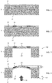
Figures 1-3 show steps of a process for forming a microelectromechanical system (MEMS) pressure sensor; -
Figures 4-5 illustrate a response of the sensor ofFigure 3 to the application of pressure; -
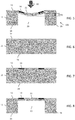
Figures 6-10B show steps of a process for forming a microelectromechanical system (MEMS) pressure sensor; -
Figures 11A and11B illustrate a response of the sensor ofFigures 10A and10B , respectively, to the application of pressure; and -
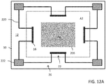
Figures 12A-12C are plan views showing example layouts for the stress structure with piezoresistors in a bridge circuit configuration for the sensor. - Reference is made to
Figures 1-3 which show steps in a process for forming a microelectromechanical system (MEMS)pressure sensor 100.Figure 1 shows asemiconductor substrate 10 that is, for example, made of silicon. Thesubstrate 10 may, if desired, be lightly doped with a dopant of a first conductivity type (for example, n-type) or may be left as intrinsic semiconductor material. Thesubstrate 10 includes atop surface 12 and abottom surface 14. Using a conventional lithographic process, a plurality of dopedregions 16 are formed in thesubstrate 10 at thetop surface 12. The dopedregions 16 may, for example, be formed using a masked implantation and activation of a dopant of a second conductivity type (for example, p-type). As an example, thedoped regions 16 have a dopant concentration suitable for forming a resistive semiconductor structure. The result is shown inFigure 2 . Thebottom surface 14 of thesubstrate 10 is then micromachined in order to selectively thin thesubstrate 10 and form a blind opening (or cavity) 20 extending into the substrate from thebottom surface 14, where the blind opening defines athin membrane 22 at thetop surface 12. Thethin membrane 22 has a thickness which permits bending in response to application of a pressure to be sensed. The plurality of dopedregions 16 are located within the area of thethin membrane 22 at thetop surface 12. The result is shown inFigure 3 . The portions of thesubstrate 10 which are not thinned form asubstrate frame 26 from which thethin membrane 22 is suspended. The substantially flat shape of thethin membrane 22 as shown inFigure 3 is the normal or initial state of thesensor 100. - By making an electrical connection to the
doped region 16 at two distinct, spaced apart, locations, each dopedregion 16 may form a semiconductor resistor (for example, of the piezoresistive type) such that the resistance between the two electrical connections varies as a function of displacement (i.e., bending) of thethin membrane 22. Thethin membrane 22 may be bent in a first direction, away from the normal or initial state, in response to apressure 30 applied in the direction of thebottom surface 14 as shown inFigure 4 . The amount of displacement Xpos by which thethin membrane 22 is bent is a function of the magnitude of the appliedpressure 30, and the change of resistance of the piezoresistive resistors formed by the includeddoped regions 16 will correspondingly vary as a function of the magnitude of the appliedpressure 30. Thethin membrane 22 may also be bent in a second direction, opposite the first direction, away from the normal or initial state, in response to apressure 32 applied to thetop surface 12 as shown inFigure 5 . The amount of displacement Xneg by which thethin membrane 22 is bent is a function of the magnitude of the appliedpressure 32, and the change of resistance of the piezoresistive resistors formed by the includeddoped regions 16 will correspondingly vary as a function of the magnitude of the appliedpressure 32. It will be noted that the sensitivity range for thesensor 100 is limited by the maximum value of the amount of displacement (Xpos, or Xneg) due to the bending of thethin membrane 22. - Reference is made to
Figures 6-10B which show steps in a process for forming a microelectromechanical system (MEMS)pressure sensor 200.Figure 6 shows asemiconductor substrate 10 that is, for example, made of silicon. Thesubstrate 10 may, if desired, be lightly doped with a dopant of a first conductivity type (for example, n-type) or may be left as intrinsic semiconductor material. Thesubstrate 10 includes atop surface 12 and abottom surface 14. Using a conventional lithographic process, a plurality ofdoped regions 16 are formed in thesubstrate 10 at thetop surface 12. The dopedregions 16 may, for example, be formed using a masked implantation and activation of a dopant of a second conductivity type (for example, p-type). As an example, the dopedregions 16 have a dopant concentration suitable for forming a resistive semiconductor structure. The result is shown inFigure 7 . Thebottom surface 14 of thesubstrate 10 is then micromachined in order to selectively thin thesubstrate 10 and form a blind opening (or cavity) 20 extending into the substrate from thebottom surface 14, wherein the blind opening defines athin membrane 22 at thetop surface 12. The thin membrane has a thickness which permits bending in response to application of a pressure to be sensed. The plurality ofdoped regions 16 are located within the area of thethin membrane 22 at thetop surface 12. The result is shown inFigure 8 . The portions of thesubstrate 10 which are not thinned form asubstrate frame 26 from which thethin membrane 22 is suspended. Next, alayer 202 of a material is deposited on atopside surface 203 of thethin membrane 22 in the middle of the area of thethin membrane 22. The deposited material may, for example, comprise a polyimide. The area occupied by thelayer 202 is less than the area of thethin membrane 22. The result is shown inFigure 9A . A curing process is then performed with respect to thelayer 202 and as a result thelayer 202 shrinks to form astress structure 206 which induces a deformation of thethin membrane 22 due to residual stress with a convex shape on thebottomside surface 204 of the thin membrane 22 (and a concave shape on thetopside surface 203 of the thin membrane 22). The result is shown inFigure 10A . The deformed shape of thethin membrane 22 as shown inFigure 10A is the normal or initial state of thesensor 200. The curing process may comprise, after deposition of thelayer 202, a prebake (for example, at a temperature of about 240°C), followed by an exposure to ultra-violet light in a contact aligner (with a dose of about 420 mj), followed by an atmospheric oven bake (for example, at a temperature of about 350°C). - In an alternative embodiment, the
layer 202 of the material is deposited within theopening 20 on thebottomside surface 204 of thethin membrane 22 in the middle of the area of thethin membrane 22. Again the deposited material may comprise a polyimide, and the area occupied by thelayer 202 is less than the area of thethin membrane 22. The result is shown inFigure 9B . The curing process as discussed above is then performed to form astress structure 206 which induces a deformation of thethin membrane 22 due to residual stress with a convex shape on thetopside surface 203 of the thin membrane 22 (and a concave shape on thebottomside surface 204 of the thin membrane 22). The result is shown inFigure 10B . The deformed shape of thethin membrane 22 as shown inFigure 10B is the normal or initial state of thesensor 200. - It will be noted that in the normal or initial state of the
sensor 200, for each of the embodiments shown byFigures 10A and10B , thestress structure 206 is located on the surface of thethin membrane 22 which is associated with the concave shape as a result of the residual stress from the stress structure. The opposite surface of thethin membrane 22, which is associated with the convex shape, forms the pressure sensing surface of thesensor 200. Thus, in theFigure 10A embodiment thebottomside surface 204 of thethin membrane 22 is the pressure sensing surface, while in theFigure 10B embodiment thetopside surface 203 of thethin membrane 22 is the pressure sensing surface. The use of thestress structure 206 forms a sensor where thethin membrane 22 is biased in a deformed shape for the normal or initial state, deflects from that deformed shape in response to an applied pressure at the convex shaped surface (in an opposite direction from the deformed shape) and is resilient so as to return to that deformed shape when the pressure is removed. - It is important to note that the thinning of the
substrate 10 to form theblind opening 20 must be controlled so as to set the thickness of thethin membrane 22 in a manner which permits thestress structure 206 to induce the required degree of deformation of thethin membrane 22 for the normal or initial state. - By making an electrical connection to the doped
region 16 at two distinct, spaced apart, locations, each dopedregion 16 may form a semiconductor resistor (for example, of the piezoresistive type) such that the resistance between the two electrical connections varies as a function of displacement (i.e., bending) of thethin membrane 22. With respect to the embodiment of thesensor 200 as shown inFigure 10A , thethin membrane 22 may be bent in a direction opposite the biased deformation induced by thestress structure 206, which defines the normal or initial state, in response to apressure 30 applied in the direction of thebottom surface 14 as shown inFigure 11A . The amount of displacement Xpos by which thethin membrane 22 bends is a function of the magnitude of the appliedpressure 30, and the change of resistance of the piezoresistive resistors formed by the includeddoped regions 16 will correspondingly vary as a function of the magnitude of the appliedpressure 30. It will be noted that the magnitude of the displacement Xpos for the bending inFigure 11A in response to the applied pressure is substantially greater (for example, at about 2X) the magnitude of displacement Xpos of the bending inFigure 4 . Thus, thesensor 200 exhibits a greater sensitivity and range than thesensor 100. - With respect to the embodiment of the
sensor 200 as shown inFigure 10B , thethin membrane 22 may be bent in a direction opposite the biased deformation induced by thestress structure 206, which defines the normal or initial state, in response to apressure 32 applied in the direction of thetop surface 12 as shown inFigure 11B . The amount of displacement Xneg by which thethin membrane 22 bends is a function of the magnitude of the appliedpressure 32, and the change of resistance of the piezoresistive resistors formed by the includeddoped regions 16 will correspondingly vary as a function of the magnitude of the appliedpressure 32. It will be noted that the magnitude of displacement Xneg for the bending inFigure 11B is substantially greater (for example, at about 2X) the magnitude of displacement Xneg of bending inFigure 5 . Thus, thesensor 200 exhibits a greater sensitivity and range than thesensor 100. - Reference is now made to
Figure 12A which is a plan view showing an example layout of thestress structure 206 with piezoresistors in a bridge circuit configuration for the sensor. The sensor includes four dopedregions 16 forming four corresponding piezoresistors. The dotted line shows the area of thethin membrane 22 as defined by theopening 20. Thestress structure 206 is shown in this view on thetop surface 12 of thesubstrate 10 corresponding to the implementation ofFigure 10A . However, it will be understood that thestress structure 206 could alternatively be positioned on thebottomside surface 204 in theopening 20 as shown in the implementation ofFigure 10B . - The area A1 occupied by the
stress structure 206 is less than the area A2 of thethin membrane 22. Thestress structure 206 is offset from, and in a preferred embodiment centered between, the fourdoped regions 16. Indeed, in the preferred embodiment the geometric center of the area A1 occupied by thestress structure 206 coincides with the geometric center of the area A2 occupied by thethin membrane 22. Thethin membrane 22 defined by theopening 20 and thestress structure 206 may each have, in plan view, a quadrilateral shape. The fourdoped regions 16 are arranged to longitudinally extend parallel to a corresponding side of thestress structure 206. Furthermore, a center of the longitudinal extension of each dopedregion 16 is located in alignment with the center of corresponding side of thethin membrane 22 in order to ensure maximal stress. -
Circuit lines 220 are formed above, and insulated from, thetop surface 12 of thesubstrate 10, with thosecircuit lines 220 interconnectingelectrical connection pads 222 of the sensor to the fourdoped regions 16 through vias (not explicitly shown, but located at positions to make electrical contact to the spaced apart locations for each doped region 16). The electrical circuit formed by the illustrated electrical connections forms a resistive bridge circuit, and variation in the resistance of the bridge circuit can be sensed using a sensing circuit connected to thepads 222 in order to sense the appliedpressure -
Figure 12A shows the plan view for thestress structure 206 having a quadrilateral shape (which may be rectangular (as show) or square, for example). In an alternative implementation shown inFigure 12B , thestress structure 206 has a round shape in the plan view (where that round shape may be circular or ovular). The circular shape of the stress structure, for example, induces circular residual stress on thethin membrane 22 and this will alter both the response of the membrane to the appliedpressure Figure 12C , thestress structure 206 has a more complex shape in the plan view. The complex shape for thestress structure 206 comprises acentral region 206c (which may have any desired shape including quadrilateral and round (as shown)) and one ormore arms 206a which radially extend from thecentral region 206c. In a preferred implementation, each included radially extendingarm 206a is oriented in a direction extending towards a corresponding one of the piezoresistors (that direction preferably being perpendicular to the longitudinal extension of the doped region forming the piezoresistor). The advantage of the complex shape for thestress structure 206 is that thearms 206a protrude residual stress further away from the geometric center of thethin membrane 22. It will be noted than an imbalance in the residual stress induced by thestress structure 206 can be applied by including less than fourarms 206a and/or by having the included arms 206s present different radial lengths. - While the invention has been illustrated and described in detail in the drawings and foregoing description, such illustration and description are considered illustrative or exemplary and not restrictive; the invention is not limited to the disclosed embodiments. Other variations to the disclosed embodiments can be understood and effected by those skilled in the art in practicing the claimed invention, from a study of the drawings, the disclosure, and the appended claims.
Claims (14)
- A sensor, comprising:a semiconductor substrate having a top surface and a bottom surface and including a blind opening extending into the semiconductor substrate from the bottom surface, said blind opening defining a thin membrane suspended from a substrate frame, wherein the thin membrane has a topside surface and a bottomside surface;a stress structure mounted to one of the topside surface or bottomside surface of the thin membrane and configured to induce a bending of the thin membrane which defines a normal state for the thin membrane; anda plurality of piezoresistors supported by the thin membrane.
- The sensor of claim 1, wherein the stress structure is mounted to the topside surface of the thin membrane and the induced bending of the thin membrane forms a concave shape at the topside surface and a convex shape at the bottomside surface.
- The sensor of claim 2, wherein the sensor functions to sense pressure applied in a direction towards the bottomside surface which produces a bending of the thin membrane away from the normal state.
- The sensor of claim 1, wherein the stress structure is mounted to the bottomside surface of the thin membrane and the induced bending of the thin membrane forms a concave shape at the bottomside surface and a convex shape at the topside surface.
- The sensor of claim 4, wherein the sensor functions to sense pressure applied in a direction towards the topside surface which produces a bending of the thin membrane away from the normal state.
- A pressure sensor, comprising:a semiconductor frame surrounding an opening;a semiconductor membrane suspended from the semiconductor frame over the opening;a plurality of piezoresistors supported by the semiconductor membrane; anda stress structure mounted to a surface of the semiconductor membrane and configured to induce a bending of the semiconductor membrane to produce a convex surface which defines a normal state for the semiconductor membrane;wherein the semiconductor membrane responds to an applied pressure at the convex surface by deforming from the normal state in a direction away from the applied pressure;wherein a resistance of the plurality of piezoresistors changes in response to the deformation of the semiconductor membrane.
- The pressure sensor of claim 6, wherein the surface of the semiconductor membrane on which is mounted the stress structure is the topside surface of the semiconductor substrate.
- The pressure sensor of claim 6, wherein the surface of the semiconductor membrane on which is mounted the stress structure is the bottomside surface of the semiconductor substrate.
- The sensor of anyone of claims 1 to 8, wherein each piezoresistor is formed by a doped region at the topside surface of the membrane.
- The sensor of anyone of claims 1 to 9, wherein the opening defines the membrane to have, in plan view, a quadrilateral shape.
- The sensor of anyone of claim 1 to 10, wherein the stress structure, in plan view, has a quadrilateral shape, and wherein sides of the stress structure extend parallel to sides of the opening.
- The sensor of anyone of claims 1 to 11, wherein the stress structure, in plan view, has a quadrilateral shape, and wherein each piezoresistor longitudinally extends parallel to a side of the stress structure.
- The sensor of anyone of claims 1 to 12, wherein the stress structure, in plan view, has a round shape.
- The sensor of claim 13, wherein the stress structure, in plan view, further includes one or more arms which radially extend from the round shape.
Applications Claiming Priority (2)
| Application Number | Priority Date | Filing Date | Title |
|---|---|---|---|
| US202062961510P | 2020-01-15 | 2020-01-15 | |
| US17/115,137 US20210214211A1 (en) | 2020-01-15 | 2020-12-08 | Mems thin membrane with stress structure |
Publications (2)
| Publication Number | Publication Date |
|---|---|
| EP3851822A1 true EP3851822A1 (en) | 2021-07-21 |
| EP3851822B1 EP3851822B1 (en) | 2026-02-25 |
Family
ID=74103921
Family Applications (1)
| Application Number | Title | Priority Date | Filing Date |
|---|---|---|---|
| EP21150139.0A Active EP3851822B1 (en) | 2020-01-15 | 2021-01-05 | Mems thin membrane with stress structure |
Country Status (3)
| Country | Link |
|---|---|
| US (2) | US20210214211A1 (en) |
| EP (1) | EP3851822B1 (en) |
| CN (2) | CN215492156U (en) |
Families Citing this family (2)
| Publication number | Priority date | Publication date | Assignee | Title |
|---|---|---|---|---|
| US20210214211A1 (en) * | 2020-01-15 | 2021-07-15 | Stmicroelectronics Pte Ltd | Mems thin membrane with stress structure |
| US11650110B2 (en) * | 2020-11-04 | 2023-05-16 | Honeywell International Inc. | Rosette piezo-resistive gauge circuit for thermally compensated measurement of full stress tensor |
Citations (2)
| Publication number | Priority date | Publication date | Assignee | Title |
|---|---|---|---|---|
| US20120227505A1 (en) * | 2011-03-09 | 2012-09-13 | Opsens Inc. | Miniature high sensitivity pressure sensor |
| EP3095754A1 (en) * | 2015-05-22 | 2016-11-23 | Amphenol Thermometrics, Inc. | Low pressure sensor and flow sensor |
Family Cites Families (19)
| Publication number | Priority date | Publication date | Assignee | Title |
|---|---|---|---|---|
| JPH08279621A (en) * | 1995-04-03 | 1996-10-22 | Motorola Inc | Balanced pressure sensor and its method |
| JP2000214027A (en) * | 1999-01-26 | 2000-08-04 | Matsushita Electric Works Ltd | Semiconductor pressure sensor |
| US6056888A (en) * | 1999-04-19 | 2000-05-02 | Motorola, Inc. | Electronic component and method of manufacture |
| US6268642B1 (en) * | 1999-04-26 | 2001-07-31 | United Microelectronics Corp. | Wafer level package |
| US6634113B1 (en) * | 2002-05-17 | 2003-10-21 | Delphi Technologies, Inc. | Tilt sensor and method of forming such device |
| DE10231727A1 (en) * | 2002-07-13 | 2004-01-22 | Robert Bosch Gmbh | Micromechanical pressure sensor device and corresponding measuring arrangement |
| JP4003686B2 (en) * | 2003-04-10 | 2007-11-07 | 株式会社村田製作所 | Piezoelectric electroacoustic transducer |
| JP2006319945A (en) * | 2005-04-12 | 2006-11-24 | Osaka Industrial Promotion Organization | Diaphragm type sensor element and manufacturing method thereof |
| JP2008203102A (en) * | 2007-02-20 | 2008-09-04 | Osaka Univ | Method for manufacturing cantilever and force sensor |
| DE102008000439B4 (en) * | 2008-02-28 | 2011-03-17 | Wika Alexander Wiegand Gmbh & Co. Kg | Pressure transducer with a membrane |
| US8237324B2 (en) * | 2008-12-10 | 2012-08-07 | The Regents Of The University Of California | Bistable electroactive polymers |
| JP5751026B2 (en) * | 2011-05-31 | 2015-07-22 | セイコーエプソン株式会社 | Ultrasonic transducer, biosensor, and method for manufacturing ultrasonic transducer |
| US9402137B2 (en) * | 2011-11-14 | 2016-07-26 | Infineon Technologies Ag | Sound transducer with interdigitated first and second sets of comb fingers |
| CN103364118A (en) * | 2012-03-29 | 2013-10-23 | 中国科学院电子学研究所 | Piezoresistive pressure sensor and manufacturing method thereof |
| KR101959150B1 (en) * | 2014-10-07 | 2019-03-15 | 히타치 긴조쿠 가부시키가이샤 | Pressure sensor, differential pressure sensor, and mass flow rate control device using same |
| CN205785644U (en) * | 2016-06-23 | 2016-12-07 | 龙微科技无锡有限公司 | MEMS minute-pressure pressure transducer |
| KR101990706B1 (en) * | 2017-12-05 | 2019-06-18 | 전자부품연구원 | Pressure sensor and manufacturing method thereof |
| CN108981982A (en) * | 2018-06-05 | 2018-12-11 | 无锡莱顿电子有限公司 | A kind of MEMS pressure sensor and preparation method thereof |
| US20210214211A1 (en) * | 2020-01-15 | 2021-07-15 | Stmicroelectronics Pte Ltd | Mems thin membrane with stress structure |
-
2020
- 2020-12-08 US US17/115,137 patent/US20210214211A1/en not_active Abandoned
-
2021
- 2021-01-05 EP EP21150139.0A patent/EP3851822B1/en active Active
- 2021-01-14 CN CN202120093455.8U patent/CN215492156U/en active Active
- 2021-01-14 CN CN202110046972.4A patent/CN113125056B/en active Active
-
2025
- 2025-01-21 US US19/033,227 patent/US20250171294A1/en active Pending
Patent Citations (2)
| Publication number | Priority date | Publication date | Assignee | Title |
|---|---|---|---|---|
| US20120227505A1 (en) * | 2011-03-09 | 2012-09-13 | Opsens Inc. | Miniature high sensitivity pressure sensor |
| EP3095754A1 (en) * | 2015-05-22 | 2016-11-23 | Amphenol Thermometrics, Inc. | Low pressure sensor and flow sensor |
Also Published As
| Publication number | Publication date |
|---|---|
| CN113125056B (en) | 2024-01-02 |
| US20250171294A1 (en) | 2025-05-29 |
| CN113125056A (en) | 2021-07-16 |
| CN215492156U (en) | 2022-01-11 |
| EP3851822B1 (en) | 2026-02-25 |
| US20210214211A1 (en) | 2021-07-15 |
Similar Documents
| Publication | Publication Date | Title |
|---|---|---|
| US20250171294A1 (en) | Mems thin membrane with stress structure | |
| JP3259102B2 (en) | Overpressure prevention type differential pressure sensor and method of manufacturing the same | |
| JP4298807B2 (en) | Integrated piezoresistive pressure sensor and method of manufacturing the same | |
| CN206126837U (en) | MEMS pressure sensor with little mechanical structure | |
| US5323656A (en) | Overpressure-protected, polysilicon, capacitive differential pressure sensor and method of making the same | |
| EP1359402B1 (en) | Pressure sensor | |
| US7150195B2 (en) | Sealed capacitive sensor for physical measurements | |
| US6861276B2 (en) | Method for fabricating a single chip multiple range pressure transducer device | |
| CN110044524B (en) | Micro-electromechanical piezoresistive pressure sensor with self-test capability and corresponding manufacturing method | |
| WO1993012410A1 (en) | Piezoresistive silicon pressure sensor design | |
| KR100555665B1 (en) | Complex sensor and manufacturing method | |
| CN110577185B (en) | MEMS structure, manufacturing method of MEMS structure and tire pressure sensor | |
| JP2002250665A (en) | Capacitive sensor and method of manufacturing the same | |
| US5317922A (en) | Capacitance transducer article and method of fabrication | |
| JPS6345050B2 (en) | ||
| CN113483925A (en) | MEMS piezoresistive pressure sensor and preparation method thereof | |
| JP5057606B2 (en) | Electronic component and manufacturing method | |
| US10741746B2 (en) | Pressure sensor and manufacturing method thereof | |
| US20180027337A1 (en) | Piezoresistive microphone and method of fabricating the same | |
| KR101794764B1 (en) | Mems pressure sensor and manufacturing method thereof | |
| CN115014593B (en) | Pressure sensor and preparation method thereof | |
| JPH07318445A (en) | Capacitive pressure sensor and manufacturing method thereof | |
| JP2002340714A (en) | Semiconductor pressure sensor and its manufacturing method | |
| JP6882850B2 (en) | Stress sensor | |
| JP6908355B2 (en) | Stress sensor |
Legal Events
| Date | Code | Title | Description |
|---|---|---|---|
| PUAI | Public reference made under article 153(3) epc to a published international application that has entered the european phase |
Free format text: ORIGINAL CODE: 0009012 |
|
| STAA | Information on the status of an ep patent application or granted ep patent |
Free format text: STATUS: REQUEST FOR EXAMINATION WAS MADE |
|
| 17P | Request for examination filed |
Effective date: 20210105 |
|
| AK | Designated contracting states |
Kind code of ref document: A1 Designated state(s): AL AT BE BG CH CY CZ DE DK EE ES FI FR GB GR HR HU IE IS IT LI LT LU LV MC MK MT NL NO PL PT RO RS SE SI SK SM TR |
|
| STAA | Information on the status of an ep patent application or granted ep patent |
Free format text: STATUS: EXAMINATION IS IN PROGRESS |
|
| 17Q | First examination report despatched |
Effective date: 20230602 |
|
| GRAP | Despatch of communication of intention to grant a patent |
Free format text: ORIGINAL CODE: EPIDOSNIGR1 |
|
| STAA | Information on the status of an ep patent application or granted ep patent |
Free format text: STATUS: GRANT OF PATENT IS INTENDED |
|
| INTG | Intention to grant announced |
Effective date: 20251017 |
|
| GRAS | Grant fee paid |
Free format text: ORIGINAL CODE: EPIDOSNIGR3 |
|
| GRAA | (expected) grant |
Free format text: ORIGINAL CODE: 0009210 |
|
| STAA | Information on the status of an ep patent application or granted ep patent |
Free format text: STATUS: THE PATENT HAS BEEN GRANTED |
|
| AK | Designated contracting states |
Kind code of ref document: B1 Designated state(s): AL AT BE BG CH CY CZ DE DK EE ES FI FR GB GR HR HU IE IS IT LI LT LU LV MC MK MT NL NO PL PT RO RS SE SI SK SM TR |
|
| REG | Reference to a national code |
Ref country code: CH Ref legal event code: F10 Free format text: ST27 STATUS EVENT CODE: U-0-0-F10-F00 (AS PROVIDED BY THE NATIONAL OFFICE) Effective date: 20260225 Ref country code: GB Ref legal event code: FG4D |
|
| REG | Reference to a national code |
Ref country code: DE Ref legal event code: R096 Ref document number: 602021048517 Country of ref document: DE |
|
| REG | Reference to a national code |
Ref country code: IE Ref legal event code: FG4D |