EP3849085A2 - Systems and methods for providing bi-directional signal level shifting - Google Patents
Systems and methods for providing bi-directional signal level shifting Download PDFInfo
- Publication number
- EP3849085A2 EP3849085A2 EP20212729.6A EP20212729A EP3849085A2 EP 3849085 A2 EP3849085 A2 EP 3849085A2 EP 20212729 A EP20212729 A EP 20212729A EP 3849085 A2 EP3849085 A2 EP 3849085A2
- Authority
- EP
- European Patent Office
- Prior art keywords
- signal line
- level
- transistor
- voltage
- upstream
- Prior art date
- Legal status (The legal status is an assumption and is not a legal conclusion. Google has not performed a legal analysis and makes no representation as to the accuracy of the status listed.)
- Pending
Links
- 238000000034 method Methods 0.000 title description 5
- 238000011144 upstream manufacturing Methods 0.000 claims description 44
- 230000006854 communication Effects 0.000 description 14
- 238000004891 communication Methods 0.000 description 14
- 238000010586 diagram Methods 0.000 description 5
- 230000005540 biological transmission Effects 0.000 description 3
- 239000003990 capacitor Substances 0.000 description 2
- 238000012544 monitoring process Methods 0.000 description 2
- 230000007175 bidirectional communication Effects 0.000 description 1
- 230000007423 decrease Effects 0.000 description 1
- 238000012986 modification Methods 0.000 description 1
- 230000004048 modification Effects 0.000 description 1
- 230000001012 protector Effects 0.000 description 1
Images

Classifications
-
- H—ELECTRICITY
- H03—ELECTRONIC CIRCUITRY
- H03K—PULSE TECHNIQUE
- H03K19/00—Logic circuits, i.e. having at least two inputs acting on one output; Inverting circuits
- H03K19/0175—Coupling arrangements; Interface arrangements
- H03K19/0185—Coupling arrangements; Interface arrangements using field effect transistors only
- H03K19/018592—Coupling arrangements; Interface arrangements using field effect transistors only with a bidirectional operation
-
- H—ELECTRICITY
- H03—ELECTRONIC CIRCUITRY
- H03K—PULSE TECHNIQUE
- H03K3/00—Circuits for generating electric pulses; Monostable, bistable or multistable circuits
- H03K3/02—Generators characterised by the type of circuit or by the means used for producing pulses
- H03K3/353—Generators characterised by the type of circuit or by the means used for producing pulses by the use, as active elements, of field-effect transistors with internal or external positive feedback
- H03K3/356—Bistable circuits
- H03K3/356017—Bistable circuits using additional transistors in the input circuit
-
- H—ELECTRICITY
- H03—ELECTRONIC CIRCUITRY
- H03K—PULSE TECHNIQUE
- H03K19/00—Logic circuits, i.e. having at least two inputs acting on one output; Inverting circuits
- H03K19/0175—Coupling arrangements; Interface arrangements
- H03K19/018—Coupling arrangements; Interface arrangements using bipolar transistors only
- H03K19/01843—Coupling arrangements; Interface arrangements using bipolar transistors only with a bidirectional operation
-
- F—MECHANICAL ENGINEERING; LIGHTING; HEATING; WEAPONS; BLASTING
- F16—ENGINEERING ELEMENTS AND UNITS; GENERAL MEASURES FOR PRODUCING AND MAINTAINING EFFECTIVE FUNCTIONING OF MACHINES OR INSTALLATIONS; THERMAL INSULATION IN GENERAL
- F16P—SAFETY DEVICES IN GENERAL; SAFETY DEVICES FOR PRESSES
- F16P3/00—Safety devices acting in conjunction with the control or operation of a machine; Control arrangements requiring the simultaneous use of two or more parts of the body
-
- H—ELECTRICITY
- H03—ELECTRONIC CIRCUITRY
- H03K—PULSE TECHNIQUE
- H03K19/00—Logic circuits, i.e. having at least two inputs acting on one output; Inverting circuits
- H03K19/0175—Coupling arrangements; Interface arrangements
- H03K19/01759—Coupling arrangements; Interface arrangements with a bidirectional operation
-
- H—ELECTRICITY
- H03—ELECTRONIC CIRCUITRY
- H03K—PULSE TECHNIQUE
- H03K19/00—Logic circuits, i.e. having at least two inputs acting on one output; Inverting circuits
- H03K19/0175—Coupling arrangements; Interface arrangements
- H03K19/0185—Coupling arrangements; Interface arrangements using field effect transistors only
- H03K19/018557—Coupling arrangements; Impedance matching circuits
Definitions
- This application relates generally to systems and methods for providing signal level shifting, and, more particularly relates to systems and methods for providing bi-directional signal level shifting and providing high drive capability for capacitive loads.
- Industrial safety systems e.g., systems powered by 24V
- single-wire safety architecture utilize multiple safety devices to provide safety control and monitoring.
- the single-wire safety architecture allows signals transmitting through the safety devices bi-directionally. The signal level drops during transmission through the safety devices, and a power supply is provided at one or more desired locations between safety devices to maintain a desired signal level during the bi-directional transmission.
- the circuit shifts signal levels between a first signal line and a second signal line.
- the circuit includes a first transistor and a second transistor.
- the first transistor includes a first gate connected to the second signal line, a first source connected to the first signal line, and a first drain connected to a voltage rail which supplies voltage.
- the second transistor includes a second gate connected to the voltage rail, a second source connected to the first signal line, and a second drain connected to the second signal line.
- the power supply device includes a first terminal, a second terminal, a third terminal, and a bi-directional shift circuit.
- the first terminal is connected to an upstream device.
- the second terminal is connected to a downstream device.
- the third terminal is connected to a power source supplying voltage at a constant level.
- the bi-directional shift circuit includes a first transistor and a second transistor.
- the first transistor includes a first gate connected to a signal line of the downstream device, a first source connected to a signal line of the upstream device, and a first drain connected to a voltage rail of the upstream device.
- the second transistor includes a second gate connected to the voltage rail of the upstream device, a second source connected to the signal line of the upstream device, and a second drain connected to the signal line of the downstream device.
- the safety system includes an upstream device, a downstream device, and a power supply device disposed between the upstream device and the downstream device.
- the power supply device includes a first terminal, a second terminal, a third terminal, and a bi-directional shift circuit.
- the first terminal is connected to an upstream device.
- the second terminal is connected to a downstream device.
- the third terminal is connected to a power source supplying voltage at a constant level.
- the bi-directional shift circuit includes a first transistor and a second transistor.
- the first transistor includes a first gate connected to a signal line of the downstream device, a first source connected to a signal line of the upstream device, and a first drain connected to a voltage rail of the upstream device.
- the second transistor includes a second gate connected to the voltage rail of the upstream device, a second source connected to the signal line of the upstream device, and a second drain connected to the signal line of the downstream device.
- the safety system 100 is configured to provide safety device monitoring and controlling according to some embodiments.
- the safety system 100 includes a safety relay acting as a communications master 102, one or more safety devices 104a, 104b, and 102c, and a power supply device 106 connected in series using a single wire according to some embodiments.
- the safety devices 104a, 104b, 104c, and the power supply device 106 are configured to compliance with a single-wire safety communication protocol according to some embodiments.
- the safety device 104c which is farthest from the communications master 102 in the communication chain, serves as a safety master.
- the safety master 104c generates a defined pulse train that is passed through each safety device in the chain to the communications master 102.
- the communications master 102 remains in operational mode as long as the defined pulse train is recognized.
- the total path between the safety master 104c and the communications master 102 includes a single-wire safety plus link, which is made up of multiple sub-links between adjacent safety devices (e.g., safety devices 104c and 104b), and sub-links between adjacent safety device and the power device (e.g., the safety device 104b and the power device 106).
- the safety device When one of the safety devices identifies the loss of its safety function (e.g., opening of a safety gate, pressing of an emergency stop button, etc.) and enters the safe sate, the safety device ceases to pass the pulse train to upstream devices, preventing the signal from reaching the communications master 102. Upon detecting loss of the pulse train signal, the communications master 102 isolates power to the industrial system components (e.g., machine, industrial device, motor, etc.).
- the industrial system components e.g., machine, industrial device, motor, etc.
- the safety system 100 implements a bi-directional communication protocol on the single-wire safety channel, allowing the devices in the chain to share information, including but not limited to status data, address information, presence indication, etc., via the same channel over which the pulsed signal is sent.
- the single-wire protocol allows the safety devices to exchange request and response messages over the channel, while coordinating sending and receiving of these messages with transmission of the pulse train.
- the pulse train level may drop.
- the power supply device e.g., the power supply device 106
- the power supply device is installed in the communication chain to supply power to the downstream devices and so that the pulse train can still be transmitted to and from the safety master 104c.
- one or more power supply devices are installed in the communication chain. For example, a power supply device is installed at each location where the pulse train level drops to or below the threshold level according to some embodiments. More details of the power supply device are described herein.
- the power supply device 106 is configured to supply power to the pulse train in order to boost the pulse train level to a desired level.
- the power supply may cause a signal level difference that needs to be shifted down as it transmits upstream to the next safety device.
- the signal level difference may be in the range of 20V to 30V according to some embodiments.
- signals can be transmitted bi-directionally on the communication train, the power supply device 106 is thus configured to shift the level of signal transmitted through the power supply device from both directions (e.g., upstream and downstream directions).
- the power supply device 106 includes terminals 108, 110, 112, and 114, according to some embodiments.
- the terminal 108 is connected to a power supply 116 (e.g., 24 V power supply).
- the power supply 116 provides a constant power level supply.
- the terminal 110 is used for a single wire safety enabled device. In some embodiments, the terminal 110 is connected to a shorting plug 118 to allow the communication signal to pass through the terminal 110 to the terminal 112.
- the terminal 112 is connected to a downstream safety device (e.g., the safety device 104b).
- the terminal 114 is connected to an upstream safety device (e.g., the safety device 104a).
- the terminal 114 and the terminal 112 are used to transmit and/or receive signals.
- each terminal may have multiple ports (e.g., signal port, ground port, power port, etc.).
- the power supply device is configured to supply power for a safety system according to some embodiments.
- the power supply device may be used as the power supply device 106 as described above with reference to FIG. 1 .
- the power supply device 106 includes a bi-directional shift circuit 200 configured to bi-directionally shifting signal levels.
- the bi-directional shift circuit 200 includes a first terminal 208, a second terminal 210, and a third terminal 212, according to some embodiments.
- the first terminal 208 is configured to connect to a first port of the terminal 114 of the power supply device 106.
- the first terminal 208 receives power supply from the first port of the terminal 114.
- the first terminal 208 is connected to the terminal 114 through a filter 211.
- the filter 211 is configured to filter the input and/or output signal according to some embodiments.
- the second terminal 210 transmits and/or receives signal to/from an upstream safety device (e.g., the safety device 104a) through the first port of the terminal 114.
- an upstream safety device e.g., the safety device 104a
- the second terminal 210 is connected to the terminal 114 through a filter 213.
- the filter 213 is configured to filter the input and/or output signal according to some embodiments.
- the third terminal 212 is configured to connect to a port of the third terminal 112 to transmit and/or receive signal to/from a downstream safety device through the third terminal 112.
- the terminals 108, 110, 112, and 114 may include ports for grounding, power supply, etc.
- the bi-directional shift circuit 200 is shown according to an illustrative embodiment.
- the bi-directional shift circuit 200 is configured to providing bi-direction level shifting.
- the bi-directional shift circuit 200 can be used in the power supply device 106 to shift signal levels to a desired voltage range bi-directionally with high speed and high drive capability.
- the bi-directional shift circuit 200 is configured to shift high voltages down in the 20V to 30V range while providing high speed drive capability for capacitive loads.
- the bi-directional shift circuit 200 is configured to shift high voltages down to a level that is higher than 30V.
- the bi-directional shift circuit 200 is implemented as an integrated circuit.
- the bi-directional shift circuit 200 is configured to provide bi-directional level shift for signals received at the second terminal 210 and signals received at the third terminal 212 according to some embodiments.
- the second terminal 210 is connected to the upstream safety device (e.g., safety device 104a) and the third terminal 212 is connected to the downstream safety device (e.g., safety device 104b). And thus, the signal received at the second terminal 210 has a lower voltage level than the signal received at the third terminal 212.
- the bi-directional shift circuit 200 downshifts signal received at the third terminal 212 and outputs to the second terminal 210.
- the bi-directional shift circuit 200 includes a first transistor 202, a second transistor 204, and a diode 206.
- the transistors 202 and 204 are shown to be N-type MOS transistor. However, it should be understood that any appropriate type of transistors can be used herein with or without adaption.
- the first terminal 208 is connected to a drain of the first transistor 202 through a first resistor 214, according to some embodiments.
- a source of the first transistor 202 is connected to the second terminal 210, according to some embodiments .
- a gate of the first transistor 202 is connected to the third terminal 212.
- the first terminal 208 is connected to a gate of the second transistor 204 through a second resistor 216, according to some embodiments.
- a source of the second transistor 204 is connected to the second terminal 210, according to some embodiments.
- a drain of the second transistor 204 is connected to the third terminal 212, according to some embodiments.
- the diode 206 is connected in forward biased between the second terminal 210 and the third terminal 212 and is in parallel connection with the second transistor 204.
- the external diode 206 may be omitted and the internal diode of the second transistor 204 is used.
- a capacitor 218 is connected between the second terminal 210 and the third terminal 212 and is in parallel connection with the diode 206, according to some embodiments.
- an initial level at the second terminal 210 and the third terminal 212 are both 0V. Since the first terminal 208 receives the power supply rail from an upstream safety device (e.g., the safety device 104a), the voltage level of the signal is relatively lower (e.g., 20V). The lower voltage supply is provided at the gate of the second transistor 204 so that the transistor 204 is fully ON (e.g., conductive). The level at the gate of the first transistor 202 is the same as the third terminal 212, so that initially the transistor first 202 is fully OFF (e.g., nonconductive).
- a signal e.g., a pulse
- the input signal received at the second terminal 210 passes to the third terminal 212 through the conductive transistor 204 (and the diode 206) so that the level at the third terminal 212 increases as the level at the second terminal increases.
- the input signal level at the second terminal 210 is increased to a level that equals to the level at the first terminal 208 (e.g., the level at the gate of the second transistor 204) minus a turn on voltage of the transistor 204, the transistor 204 is turned OFF and the diode inside of the second transistor 204 and the diode 206 remain on to maintain the input signal level close to a full signal level.
- the signal received at the second terminal 210 decreases back to 0V
- the second transistor 204 is turned back on, and thus the signal output to the third terminal 212 is also 0V.
- an initial input signal level at the third terminal 212 and an initial output signal level at the second terminal 210 are both 0V.
- the third terminal 212 receives signal from a downstream safety device (e.g., the safety device 104b), the voltage level of the signal is relatively higher (e.g., 26V). In some embodiments, the voltage level of the signal from the downstream safety device is between 20V and 30V. In some embodiments, the voltage level of the signal from the downstream safety device is above 30V.
- the second transistor 204 is fully ON because the lower voltage power supply is applied on the gate of the transistor 204.
- the first transistor 202 is fully OFF initially because the gate level is 0V from the third terminal 212.
- the input signal received at the third terminal 212 thus passes to the second terminal 210 through the second transistor 204
- the output signal level changes along with the input signal level.
- the output signal level at the second terminal 210 increases as well.
- the transistor 204 is turned OFF.
- the input level at the third terminal 212 increases to a threshold level of the gate of the first transistor 202
- the transistor 202 is turned ON.
- the first transistor 202 is turned on, the level at the second terminal 210 is pulled up to the power supply level at the first terminal 208.
- the level at the second terminal 210 goes up to the level at the first terminal 208 as a maximum level.
- the signal level at the third terminal 212 continues increasing to a level higher than the signal level at the first terminal 208, the signal level at the second terminal 210 stays at the signal level at the first terminal 208 because the second transistor 204 is turned OFF according to some embodiments.
- the bi-directional shift circuit 200 includes a voltage divider component 220 configured to reduce voltage at the gate of the transistor when a potential voltage at the gate is above a threshold level in order to protect the transistor 204 from overloaded.
- the voltage divider component 220 includes a resistor 222 and capacitor 224.
- the protector component 220 is optional and can be removed from the bi-directional shift circuit 200. For example, when the potential voltage at the gate of the transistor 204 is below the threshold level, the voltage divider component 220 is removed from the bi-directional shift circuit 200 according to some embodiments.
- the bi-directional circuit 300 can shift high voltage in various range (e.g., voltage higher than 30V, voltage 20V-30V) depending on the parameters of the transistors 202 and 204.
Landscapes
- Engineering & Computer Science (AREA)
- Computer Hardware Design (AREA)
- General Engineering & Computer Science (AREA)
- Physics & Mathematics (AREA)
- Computing Systems (AREA)
- Mathematical Physics (AREA)
- Mechanical Engineering (AREA)
- Logic Circuits (AREA)
- Electronic Switches (AREA)
- Amplifiers (AREA)
Abstract
Description
-
US Patent Application No. 14/580,178 (granted as Patent No.9,797,552 - This application relates generally to systems and methods for providing signal level shifting, and, more particularly relates to systems and methods for providing bi-directional signal level shifting and providing high drive capability for capacitive loads.
- Industrial safety systems (e.g., systems powered by 24V) with single-wire safety architecture utilize multiple safety devices to provide safety control and monitoring. The single-wire safety architecture allows signals transmitting through the safety devices bi-directionally. The signal level drops during transmission through the safety devices, and a power supply is provided at one or more desired locations between safety devices to maintain a desired signal level during the bi-directional transmission.
- The following presents a simplified summary of the claimed subject matter in order to provide a basic understanding of some aspects described herein. This summary is not an extensive overview and is not intended to identify key/critical elements or to delineate the scope of the claimed subject matter. Its sole purpose is to present some concepts in a simplified form as a prelude to the more detailed description that is presented later.
- One embodiment of the disclosure relates to a bi-directional level shift circuit. The circuit shifts signal levels between a first signal line and a second signal line. The circuit includes a first transistor and a second transistor. The first transistor includes a first gate connected to the second signal line, a first source connected to the first signal line, and a first drain connected to a voltage rail which supplies voltage. The second transistor includes a second gate connected to the voltage rail, a second source connected to the first signal line, and a second drain connected to the second signal line.
- Another embodiment of the disclosure relates to a power supply device. The power supply device includes a first terminal, a second terminal, a third terminal, and a bi-directional shift circuit. The first terminal is connected to an upstream device. The second terminal is connected to a downstream device. The third terminal is connected to a power source supplying voltage at a constant level. The bi-directional shift circuit includes a first transistor and a second transistor. The first transistor includes a first gate connected to a signal line of the downstream device, a first source connected to a signal line of the upstream device, and a first drain connected to a voltage rail of the upstream device. The second transistor includes a second gate connected to the voltage rail of the upstream device, a second source connected to the signal line of the upstream device, and a second drain connected to the signal line of the downstream device.
- Another embodiment of the disclosure relates to a safety system. The safety system includes an upstream device, a downstream device, and a power supply device disposed between the upstream device and the downstream device. The power supply device includes a first terminal, a second terminal, a third terminal, and a bi-directional shift circuit. The first terminal is connected to an upstream device. The second terminal is connected to a downstream device. The third terminal is connected to a power source supplying voltage at a constant level. The bi-directional shift circuit includes a first transistor and a second transistor. The first transistor includes a first gate connected to a signal line of the downstream device, a first source connected to a signal line of the upstream device, and a first drain connected to a voltage rail of the upstream device. The second transistor includes a second gate connected to the voltage rail of the upstream device, a second source connected to the signal line of the upstream device, and a second drain connected to the signal line of the downstream device.
- The following description and annexed drawings set forth certain illustrative aspects of the specification. These aspects are indicative, however, of but a few of the various ways in which the principles of the specification can be employed. Other advantages and novel features of the specification will become apparent from the following detailed description of the specification when considered in conjunction with the drawings.
-
-
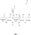
FIG. 1 is a block diagram of a safety system according to an illustrative embodiment. -
FIG. 2 is a block diagram of a power supply device used in the safety system ofFIG. 1 according to an illustrative embodiment. -
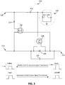
FIG. 3 depicts a bi-directional shift circuit used in the power supply device ofFIG. 2 according to an illustrative embodiment - Various aspects are now described with reference to the drawings. In the following description, for purposes of explanation, numerous specific details are set forth in order to provide a thorough understanding of one or more aspects. It may be evident, however, that such aspect(s) may be practiced without these specific details. In other instances, well-known structures and devices are shown in block diagram form in order to facilitate describing these aspects.
- Referring to
FIG. 1 , a block diagram of asafety system 100 is shown according to an illustrative embodiment. Thesafety system 100 is configured to provide safety device monitoring and controlling according to some embodiments. Thesafety system 100 includes a safety relay acting as acommunications master 102, one ormore safety devices power supply device 106 connected in series using a single wire according to some embodiments. Thesafety devices power supply device 106 are configured to compliance with a single-wire safety communication protocol according to some embodiments. - For example, the
safety device 104c, which is farthest from thecommunications master 102 in the communication chain, serves as a safety master. Thesafety master 104c generates a defined pulse train that is passed through each safety device in the chain to thecommunications master 102. Thecommunications master 102 remains in operational mode as long as the defined pulse train is recognized. The total path between thesafety master 104c and thecommunications master 102 includes a single-wire safety plus link, which is made up of multiple sub-links between adjacent safety devices (e.g.,safety devices safety device 104b and the power device 106). When one of the safety devices identifies the loss of its safety function (e.g., opening of a safety gate, pressing of an emergency stop button, etc.) and enters the safe sate, the safety device ceases to pass the pulse train to upstream devices, preventing the signal from reaching thecommunications master 102. Upon detecting loss of the pulse train signal, thecommunications master 102 isolates power to the industrial system components (e.g., machine, industrial device, motor, etc.). - In some embodiments, The
safety system 100 implements a bi-directional communication protocol on the single-wire safety channel, allowing the devices in the chain to share information, including but not limited to status data, address information, presence indication, etc., via the same channel over which the pulsed signal is sent. For example, the single-wire protocol allows the safety devices to exchange request and response messages over the channel, while coordinating sending and receiving of these messages with transmission of the pulse train. - While the pulse train level transmits through one or more safety devices (e.g., from
upstream safety device 104b todownstream safety device 104a), the pulse train level may drop. When the pulse train level drops to or below a threshold level, the power supply device (e.g., the power supply device 106) is installed in the communication chain to supply power to the downstream devices and so that the pulse train can still be transmitted to and from thesafety master 104c. In some embodiments, one or more power supply devices are installed in the communication chain. For example, a power supply device is installed at each location where the pulse train level drops to or below the threshold level according to some embodiments. More details of the power supply device are described herein. - The
power supply device 106 is configured to supply power to the pulse train in order to boost the pulse train level to a desired level. In some embodiments, where the power supply is inserted into thesafety system 100 may cause a signal level difference that needs to be shifted down as it transmits upstream to the next safety device. For example, the signal level difference may be in the range of 20V to 30V according to some embodiments. As described above, signals can be transmitted bi-directionally on the communication train, thepower supply device 106 is thus configured to shift the level of signal transmitted through the power supply device from both directions (e.g., upstream and downstream directions). Thepower supply device 106 includesterminals power supply 116 provides a constant power level supply. The terminal 110 is used for a single wire safety enabled device. In some embodiments, the terminal 110 is connected to a shortingplug 118 to allow the communication signal to pass through the terminal 110 to the terminal 112. The terminal 112 is connected to a downstream safety device (e.g., thesafety device 104b). The terminal 114 is connected to an upstream safety device (e.g., thesafety device 104a). The terminal 114 and the terminal 112 are used to transmit and/or receive signals. Although not shown in the figures, it should be understood that each terminal may have multiple ports (e.g., signal port, ground port, power port, etc.). - Referring to
FIG. 2 , a block diagram of a power supply device is shown according to an illustrative embodiment. The power supply device is configured to supply power for a safety system according to some embodiments. The power supply device may be used as thepower supply device 106 as described above with reference toFIG. 1 . Thepower supply device 106 includes abi-directional shift circuit 200 configured to bi-directionally shifting signal levels. - The
bi-directional shift circuit 200 includes afirst terminal 208, asecond terminal 210, and athird terminal 212, according to some embodiments. Thefirst terminal 208 is configured to connect to a first port of theterminal 114 of thepower supply device 106. Thefirst terminal 208 receives power supply from the first port of the terminal 114. In some embodiments, thefirst terminal 208 is connected to the terminal 114 through afilter 211. Thefilter 211 is configured to filter the input and/or output signal according to some embodiments. Thesecond terminal 210 transmits and/or receives signal to/from an upstream safety device (e.g., thesafety device 104a) through the first port of the terminal 114. In some embodiments, thesecond terminal 210 is connected to the terminal 114 through afilter 213. Thefilter 213 is configured to filter the input and/or output signal according to some embodiments. Thethird terminal 212 is configured to connect to a port of thethird terminal 112 to transmit and/or receive signal to/from a downstream safety device through thethird terminal 112. Although not shown in the figures, it should be understood that theterminals - Referring to
FIG. 3 , thebi-directional shift circuit 200 is shown according to an illustrative embodiment. Thebi-directional shift circuit 200 is configured to providing bi-direction level shifting. Thebi-directional shift circuit 200 can be used in thepower supply device 106 to shift signal levels to a desired voltage range bi-directionally with high speed and high drive capability. For example, thebi-directional shift circuit 200 is configured to shift high voltages down in the 20V to 30V range while providing high speed drive capability for capacitive loads. In some embodiments, thebi-directional shift circuit 200 is configured to shift high voltages down to a level that is higher than 30V. In some embodiments, thebi-directional shift circuit 200 is implemented as an integrated circuit. - The
bi-directional shift circuit 200 is configured to provide bi-directional level shift for signals received at thesecond terminal 210 and signals received at thethird terminal 212 according to some embodiments. In some embodiments, thesecond terminal 210 is connected to the upstream safety device (e.g.,safety device 104a) and thethird terminal 212 is connected to the downstream safety device (e.g.,safety device 104b). And thus, the signal received at thesecond terminal 210 has a lower voltage level than the signal received at thethird terminal 212. In some embodiments, thebi-directional shift circuit 200 downshifts signal received at thethird terminal 212 and outputs to thesecond terminal 210. - As shown in
FIG. 3 , thebi-directional shift circuit 200 includes afirst transistor 202, asecond transistor 204, and adiode 206. Thetransistors first terminal 208 is connected to a drain of thefirst transistor 202 through afirst resistor 214, according to some embodiments. A source of thefirst transistor 202 is connected to thesecond terminal 210, according to some embodiments . A gate of thefirst transistor 202 is connected to thethird terminal 212. - The
first terminal 208 is connected to a gate of thesecond transistor 204 through asecond resistor 216, according to some embodiments. A source of thesecond transistor 204 is connected to thesecond terminal 210, according to some embodiments. A drain of thesecond transistor 204 is connected to thethird terminal 212, according to some embodiments. In some embodiments, thediode 206 is connected in forward biased between thesecond terminal 210 and thethird terminal 212 and is in parallel connection with thesecond transistor 204. In some embodiments, theexternal diode 206 may be omitted and the internal diode of thesecond transistor 204 is used. Acapacitor 218 is connected between thesecond terminal 210 and thethird terminal 212 and is in parallel connection with thediode 206, according to some embodiments. - In operation, when a signal (e.g., a pulse) is received at the
second terminal 210, an initial level at thesecond terminal 210 and thethird terminal 212 are both 0V. Since thefirst terminal 208 receives the power supply rail from an upstream safety device (e.g., thesafety device 104a), the voltage level of the signal is relatively lower (e.g., 20V). The lower voltage supply is provided at the gate of thesecond transistor 204 so that thetransistor 204 is fully ON (e.g., conductive). The level at the gate of thefirst transistor 202 is the same as thethird terminal 212, so that initially the transistor first 202 is fully OFF (e.g., nonconductive). - With the
second transistor 204 being ON, the input signal received at the second terminal 210 passes to thethird terminal 212 through the conductive transistor 204 (and the diode 206) so that the level at thethird terminal 212 increases as the level at the second terminal increases. When the input signal level at thesecond terminal 210 is increased to a level that equals to the level at the first terminal 208 (e.g., the level at the gate of the second transistor 204) minus a turn on voltage of thetransistor 204, thetransistor 204 is turned OFF and the diode inside of thesecond transistor 204 and thediode 206 remain on to maintain the input signal level close to a full signal level. When the signal received at thesecond terminal 210 decreases back to 0V, thesecond transistor 204 is turned back on, and thus the signal output to thethird terminal 212 is also 0V. - In the opposite direction, when a signal (e.g., a pulse) is received at the
third terminal 212, an initial input signal level at thethird terminal 212 and an initial output signal level at thesecond terminal 210 are both 0V. Since thethird terminal 212 receives signal from a downstream safety device (e.g., thesafety device 104b), the voltage level of the signal is relatively higher (e.g., 26V). In some embodiments, the voltage level of the signal from the downstream safety device is between 20V and 30V. In some embodiments, the voltage level of the signal from the downstream safety device is above 30V. Initially, thesecond transistor 204 is fully ON because the lower voltage power supply is applied on the gate of thetransistor 204. Thefirst transistor 202 is fully OFF initially because the gate level is 0V from thethird terminal 212. - The input signal received at the
third terminal 212 thus passes to thesecond terminal 210 through thesecond transistor 204 The output signal level changes along with the input signal level. As the input signal level received at thethird terminal 212 increases, the output signal level at thesecond terminal 210 increases as well. When the output signal level increases to a level that equals the level at the gate terminal of thesecond transistor 204, thetransistor 204 is turned OFF. When the input level at thethird terminal 212 increases to a threshold level of the gate of thefirst transistor 202, thetransistor 202 is turned ON. When thefirst transistor 202 is turned on, the level at thesecond terminal 210 is pulled up to the power supply level at thefirst terminal 208. In this way, the level at thesecond terminal 210 goes up to the level at thefirst terminal 208 as a maximum level. When the signal level at thethird terminal 212 continues increasing to a level higher than the signal level at thefirst terminal 208, the signal level at thesecond terminal 210 stays at the signal level at thefirst terminal 208 because thesecond transistor 204 is turned OFF according to some embodiments. - In some embodiments, the
bi-directional shift circuit 200 includes avoltage divider component 220 configured to reduce voltage at the gate of the transistor when a potential voltage at the gate is above a threshold level in order to protect thetransistor 204 from overloaded. Thevoltage divider component 220 includes aresistor 222 andcapacitor 224. In some embodiments, theprotector component 220 is optional and can be removed from thebi-directional shift circuit 200. For example, when the potential voltage at the gate of thetransistor 204 is below the threshold level, thevoltage divider component 220 is removed from thebi-directional shift circuit 200 according to some embodiments. - In addition, the bi-directional circuit 300 can shift high voltage in various range (e.g., voltage higher than 30V, voltage 20V-30V) depending on the parameters of the
transistors - The subject matter as described above includes various exemplary aspects. However, it should be appreciated that it is not possible to describe every conceivable component or methodology for purposes of describing these aspects. One of ordinary skill in the art can recognize that further combinations or permutations can be possible. Various methodologies or architectures can be employed to implement the various embodiments, modifications, variations, or equivalents thereof. Accordingly, all such implementations of the aspects described herein are intended to embrace the scope and spirit of subject claims. Furthermore, to the extent that the term "includes" is used in either the detailed description or the claims, such term is intended to be inclusive in a manner similar to the term "comprising" as "comprising" is interpreted when employed as a transitional word in a claim.
Claims (15)
- A bi-directional level shift circuit shifting signal levels between a first signal line and a second signal line the circuit comprising:a first transistor comprising a first gate connected to the second signal line, a first source connected to the first signal line, and a first drain connected to a voltage rail which supplies voltage; anda second transistor comprising a second gate connected to the voltage rail, a second source connected to the first signal line, and a second drain connected to the second signal line.
- The circuit of claim 1, further comprising a diode connected in forward biased between the first signal line and the second signal line in parallel with an internal diode of the second transistor.
- The circuit of claim 1 or 2, wherein at least one of:the first transistor and the second transistor are N-type MOFET; anda voltage level of signals input from the first signal line is lower than a voltage level of signals input from the second signal line.
- The circuit of one of claims 1 to 3, wherein the first drain is connected to the voltage rail through a first resistor, and the second gate is connected to the voltage rail through a second resistor.
- The circuit of one of claims 1 to 4, wherein in response to receiving a pulse at the second signal line, the bi-directional level shift circuit outputs a pulse at the first signal line, wherein a level of the pulse at the first signal line equals to a level of the voltage supplied by the voltage rail.
- The circuit of one of claims 1 to 5, wherein in response to receiving a pulse at the first signal line, the bi-directional level shift circuit outputs a pulse at the second signal line, wherein a level of the pulse at the second signal line is substantially the same as a level of the pulse at the first signal line.
- A power supply device, comprising:a first terminal connected to an upstream device;a second terminal connected to a downstream device;a third terminal connected to a power source supplying voltage at a constant level; anda bi-directional shift circuit which comprises:a first transistor comprising a first gate connected to a signal line of the downstream device, a first source connected to a signal line of the upstream device, and a first drain connected to a voltage rail of the upstream device; anda second transistor comprising a second gate connected to the voltage rail of the upstream device, a second source connected to the signal line of the upstream device, and a second drain connected to the signal line of the downstream device.
- The power supply device of claim 7, wherein the bi-directional shift circuit further comprises a diode connected in forward biased between the signal line of the upstream device and the signal line of the downstream device in parallel with an internal diode of the second transistor.
- The power supply device of claim 7 or 8, wherein a voltage level of signals input from the signal line of the upstream device is lower than a voltage level of signals input from the signal line of the downstream device.
- The power supply device of claim 9, wherein the voltage level of signals input from the signal line of the downstream device is higher than 20V.
- The power supply device of one of claims 7 to 10, at least one of:wherein the first drain is connected to the voltage rail through a first resistor, and the second gate is connected to the voltage rail through a second resistor;wherein in response to receiving a pulse at the signal line of the downstream device, the bi-directional level shift circuit outputs a pulse at the signal line of the upstream device, wherein a level of the pulse at the signal line of the upstream device equals to a level of the voltage supplied by the voltage rail; andwherein in response to receiving a pulse at the signal line of the upstream device, the bi-directional level shift circuit outputs a pulse at the signal line of the downstream device, wherein a level of the pulse at the signal line of the downstream device is substantially the same as a level of the pulse at the signal line of the upstream device.
- A safety system comprising:an upstream device;a downstream device; anda power supply device disposed between the upstream device and the downstream device, wherein the power supply device comprises:a first terminal connected to the upstream device;a second terminal connected to the downstream device;a third terminal connected to a power source supplying voltage at a constant level; anda bi-directional shift circuit which comprises:a first transistor comprising a first gate connected to a signal line of the downstream device, a first source connected to a signal line of the upstream device, and a first drain connected to a voltage rail of the upstream device; anda second transistor comprising a second gate connected to the voltage rail of the upstream device, a second source connected to the signal line of the upstream device, and a second drain connected to the signal line of the downstream device.
- The safe system of claim 12, at least one of:wherein the bi-directional shift circuit further comprises a diode connected in forward biased between the signal line of the upstream device and the signal line of the downstream device in parallel with an internal diode of the second transistor;wherein the bi-directional shift circuit further comprises a voltage divider configured to connect between the second gate and the voltage rail of the upstream device; andwherein a voltage level of signals input from the signal line of the upstream device is lower than a voltage level of signals input from the signal line of the downstream device.
- The safe system of claim 12 or 13, further comprising a downstream end device configured to generate signals to pass through the upstream device and the power supply device to an upstream end device.
- The safe system of claim 14, wherein the upstream end device remains an operational mode in response to recognizing the signals generated by the downstream end device.
Applications Claiming Priority (1)
| Application Number | Priority Date | Filing Date | Title |
|---|---|---|---|
| US16/721,120 US11101789B2 (en) | 2019-12-19 | 2019-12-19 | Systems and methods for providing bi-directional signal level shifting |
Publications (2)
| Publication Number | Publication Date |
|---|---|
| EP3849085A2 true EP3849085A2 (en) | 2021-07-14 |
| EP3849085A3 EP3849085A3 (en) | 2021-09-01 |
Family
ID=73792941
Family Applications (1)
| Application Number | Title | Priority Date | Filing Date |
|---|---|---|---|
| EP20212729.6A Pending EP3849085A3 (en) | 2019-12-19 | 2020-12-09 | Systems and methods for providing bi-directional signal level shifting |
Country Status (3)
| Country | Link |
|---|---|
| US (1) | US11101789B2 (en) |
| EP (1) | EP3849085A3 (en) |
| CN (1) | CN113014245B (en) |
Families Citing this family (1)
| Publication number | Priority date | Publication date | Assignee | Title |
|---|---|---|---|---|
| CN117174122B (en) * | 2022-05-25 | 2026-04-17 | 联芸科技(杭州)股份有限公司 | Level conversion circuit of memory and control method of memory |
Citations (1)
| Publication number | Priority date | Publication date | Assignee | Title |
|---|---|---|---|---|
| EP2720094B1 (en) * | 2012-10-10 | 2015-05-20 | Sick Ag | Safety system |
Family Cites Families (14)
| Publication number | Priority date | Publication date | Assignee | Title |
|---|---|---|---|---|
| CA2192426C (en) | 1996-01-03 | 2000-08-01 | Richard Ng | Bidirectional voltage translator |
| US6005415A (en) * | 1997-07-18 | 1999-12-21 | International Business Machines Corporation | Switching circuit for large voltages |
| JP4416923B2 (en) * | 2000-06-23 | 2010-02-17 | Necエレクトロニクス株式会社 | Output circuit, input circuit, and semiconductor integrated circuit device |
| KR20030001926A (en) * | 2001-06-28 | 2003-01-08 | 주식회사 하이닉스반도체 | Level shifter |
| JP3836719B2 (en) | 2001-12-21 | 2006-10-25 | 日本テキサス・インスツルメンツ株式会社 | Level conversion circuit |
| DE10216226A1 (en) * | 2002-04-08 | 2003-10-30 | Pilz Gmbh & Co | Device for fail-safe switching off of an electrical consumer, especially in industrial production plants |
| US6954100B2 (en) * | 2003-09-12 | 2005-10-11 | Freescale Semiconductor, Inc. | Level shifter |
| US20050174158A1 (en) * | 2004-02-06 | 2005-08-11 | Khan Qadeer A. | Bidirectional level shifter |
| JP2008227589A (en) * | 2007-03-08 | 2008-09-25 | Matsushita Electric Ind Co Ltd | Bidirectional level shift circuit and bidirectional bus system |
| US7755412B2 (en) | 2008-04-01 | 2010-07-13 | Kyocera Corporation | Bi-directional level shifted interrupt control |
| US9846423B2 (en) * | 2014-12-22 | 2017-12-19 | Rockwell Automation Technologies, Inc. | Smart taps for a single-wire industrial safety system |
| JP6787343B2 (en) * | 2016-01-07 | 2020-11-18 | ソニー株式会社 | Comparison device, analog-to-digital converter, solid-state image sensor and image sensor |
| CN108347243B (en) * | 2017-01-25 | 2022-04-01 | 株式会社东海理化电机制作所 | Level shifter |
| US10411678B2 (en) * | 2018-02-12 | 2019-09-10 | Semiconductor Components Industries, Llc | Level-shifting circuit configured to limit leakage current |
-
2019
- 2019-12-19 US US16/721,120 patent/US11101789B2/en active Active
-
2020
- 2020-12-09 EP EP20212729.6A patent/EP3849085A3/en active Pending
- 2020-12-18 CN CN202011504104.8A patent/CN113014245B/en active Active
Patent Citations (1)
| Publication number | Priority date | Publication date | Assignee | Title |
|---|---|---|---|---|
| EP2720094B1 (en) * | 2012-10-10 | 2015-05-20 | Sick Ag | Safety system |
Also Published As
| Publication number | Publication date |
|---|---|
| CN113014245A (en) | 2021-06-22 |
| US20210194471A1 (en) | 2021-06-24 |
| US11101789B2 (en) | 2021-08-24 |
| EP3849085A3 (en) | 2021-09-01 |
| CN113014245B (en) | 2024-11-22 |
Similar Documents
| Publication | Publication Date | Title |
|---|---|---|
| US9430438B2 (en) | Communication bus with zero power wake function | |
| US9851772B2 (en) | 1-wire bus PD detection and classification scheme for ethernet PoDL | |
| US20060038661A1 (en) | Data transfer on a current supply line | |
| CN104238489B (en) | Network communication control apparatus, system and method | |
| KR20190103202A (en) | Subscriber station for bus system, and data transmission method in bus system | |
| US11101789B2 (en) | Systems and methods for providing bi-directional signal level shifting | |
| US10693451B2 (en) | Ringing suppressor circuit | |
| US5646758A (en) | Optical time compression multiplexing transmission system | |
| US20110158258A1 (en) | Communication signal processing apparatus and communication apparatus | |
| EP1213658A3 (en) | Optical communication interface module for universal serial bus | |
| US8443112B2 (en) | Input/output signal controller and input/output signal control system employing the input/output controller | |
| US7911232B2 (en) | Input/output signal controller | |
| US5809077A (en) | Circuit for signal-transmitting connection of data networks | |
| US5729547A (en) | Automatic driver/receiver control for half-duplex serial networks | |
| KR20200033340A (en) | Transceiver for bus system, and method for reducing vibration tendency when switching between different bit states | |
| US20060046766A1 (en) | Method and system for bidirectional communications and power transmission | |
| US6031348A (en) | Automatic automotive power window system and method of controlling an automatic automotive power window system | |
| US8050315B2 (en) | Open collector / open drain integrated bidirectional digital isolator | |
| US8983402B2 (en) | Transceiver with wake up detection | |
| KR101265045B1 (en) | Light-emission error preventing circuit for optical transmitter | |
| CN100511045C (en) | Peripheral module for an automation apparatus | |
| US7281151B2 (en) | Method of stopping data communication of a communication apparatus based on a detection of a power supply voltage drop | |
| ITMI20071104A1 (en) | "CONTROL DEVICE FOR A USB INTERFACE AND ITS CONTROL METHOD" | |
| DE102009027471A1 (en) | Signal transmission device and vehicle component | |
| NL2026452A (en) | Device for a subscriber station of a serial bus system and method for communication in a serial bus system |
Legal Events
| Date | Code | Title | Description |
|---|---|---|---|
| PUAI | Public reference made under article 153(3) epc to a published international application that has entered the european phase |
Free format text: ORIGINAL CODE: 0009012 |
|
| STAA | Information on the status of an ep patent application or granted ep patent |
Free format text: STATUS: THE APPLICATION HAS BEEN PUBLISHED |
|
| AK | Designated contracting states |
Kind code of ref document: A2 Designated state(s): AL AT BE BG CH CY CZ DE DK EE ES FI FR GB GR HR HU IE IS IT LI LT LU LV MC MK MT NL NO PL PT RO RS SE SI SK SM TR |
|
| PUAL | Search report despatched |
Free format text: ORIGINAL CODE: 0009013 |
|
| AK | Designated contracting states |
Kind code of ref document: A3 Designated state(s): AL AT BE BG CH CY CZ DE DK EE ES FI FR GB GR HR HU IE IS IT LI LT LU LV MC MK MT NL NO PL PT RO RS SE SI SK SM TR |
|
| RIC1 | Information provided on ipc code assigned before grant |
Ipc: H03K 19/0185 20060101AFI20210728BHEP |
|
| STAA | Information on the status of an ep patent application or granted ep patent |
Free format text: STATUS: REQUEST FOR EXAMINATION WAS MADE |
|
| 17P | Request for examination filed |
Effective date: 20220218 |
|
| RBV | Designated contracting states (corrected) |
Designated state(s): AL AT BE BG CH CY CZ DE DK EE ES FI FR GB GR HR HU IE IS IT LI LT LU LV MC MK MT NL NO PL PT RO RS SE SI SK SM TR |
|
| STAA | Information on the status of an ep patent application or granted ep patent |
Free format text: STATUS: EXAMINATION IS IN PROGRESS |
|
| 17Q | First examination report despatched |
Effective date: 20250213 |