EP3846293A1 - Circuit board shield connector - Google Patents
Circuit board shield connector Download PDFInfo
- Publication number
- EP3846293A1 EP3846293A1 EP20217571.7A EP20217571A EP3846293A1 EP 3846293 A1 EP3846293 A1 EP 3846293A1 EP 20217571 A EP20217571 A EP 20217571A EP 3846293 A1 EP3846293 A1 EP 3846293A1
- Authority
- EP
- European Patent Office
- Prior art keywords
- connection part
- circuit board
- terminal
- outer connection
- mating
- Prior art date
- Legal status (The legal status is an assumption and is not a legal conclusion. Google has not performed a legal analysis and makes no representation as to the accuracy of the status listed.)
- Withdrawn
Links
- 230000013011 mating Effects 0.000 claims abstract description 40
- 239000004020 conductor Substances 0.000 description 15
- 238000005476 soldering Methods 0.000 description 6
- 239000011810 insulating material Substances 0.000 description 2
- 230000007257 malfunction Effects 0.000 description 2
- 230000002093 peripheral effect Effects 0.000 description 2
- 229920003002 synthetic resin Polymers 0.000 description 2
- 239000000057 synthetic resin Substances 0.000 description 2
- 238000005452 bending Methods 0.000 description 1
- 238000004512 die casting Methods 0.000 description 1
- 230000000694 effects Effects 0.000 description 1
- 238000009413 insulation Methods 0.000 description 1
- 239000002184 metal Substances 0.000 description 1
- 238000012986 modification Methods 0.000 description 1
- 230000004048 modification Effects 0.000 description 1
- 238000003466 welding Methods 0.000 description 1
Images




Classifications
-
- H—ELECTRICITY
- H01—ELECTRIC ELEMENTS
- H01R—ELECTRICALLY-CONDUCTIVE CONNECTIONS; STRUCTURAL ASSOCIATIONS OF A PLURALITY OF MUTUALLY-INSULATED ELECTRICAL CONNECTING ELEMENTS; COUPLING DEVICES; CURRENT COLLECTORS
- H01R13/00—Details of coupling devices of the kinds covered by groups H01R12/70 or H01R24/00 - H01R33/00
- H01R13/648—Protective earth or shield arrangements on coupling devices, e.g. anti-static shielding
- H01R13/658—High frequency shielding arrangements, e.g. against EMI [Electro-Magnetic Interference] or EMP [Electro-Magnetic Pulse]
- H01R13/6591—Specific features or arrangements of connection of shield to conductive members
- H01R13/6594—Specific features or arrangements of connection of shield to conductive members the shield being mounted on a PCB and connected to conductive members
-
- H—ELECTRICITY
- H01—ELECTRIC ELEMENTS
- H01R—ELECTRICALLY-CONDUCTIVE CONNECTIONS; STRUCTURAL ASSOCIATIONS OF A PLURALITY OF MUTUALLY-INSULATED ELECTRICAL CONNECTING ELEMENTS; COUPLING DEVICES; CURRENT COLLECTORS
- H01R13/00—Details of coupling devices of the kinds covered by groups H01R12/70 or H01R24/00 - H01R33/00
- H01R13/648—Protective earth or shield arrangements on coupling devices, e.g. anti-static shielding
- H01R13/658—High frequency shielding arrangements, e.g. against EMI [Electro-Magnetic Interference] or EMP [Electro-Magnetic Pulse]
- H01R13/6591—Specific features or arrangements of connection of shield to conductive members
-
- H—ELECTRICITY
- H01—ELECTRIC ELEMENTS
- H01R—ELECTRICALLY-CONDUCTIVE CONNECTIONS; STRUCTURAL ASSOCIATIONS OF A PLURALITY OF MUTUALLY-INSULATED ELECTRICAL CONNECTING ELEMENTS; COUPLING DEVICES; CURRENT COLLECTORS
- H01R12/00—Structural associations of a plurality of mutually-insulated electrical connecting elements, specially adapted for printed circuits, e.g. printed circuit boards [PCB], flat or ribbon cables, or like generally planar structures, e.g. terminal strips, terminal blocks; Coupling devices specially adapted for printed circuits, flat or ribbon cables, or like generally planar structures; Terminals specially adapted for contact with, or insertion into, printed circuits, flat or ribbon cables, or like generally planar structures
- H01R12/70—Coupling devices
- H01R12/71—Coupling devices for rigid printing circuits or like structures
-
- H—ELECTRICITY
- H01—ELECTRIC ELEMENTS
- H01R—ELECTRICALLY-CONDUCTIVE CONNECTIONS; STRUCTURAL ASSOCIATIONS OF A PLURALITY OF MUTUALLY-INSULATED ELECTRICAL CONNECTING ELEMENTS; COUPLING DEVICES; CURRENT COLLECTORS
- H01R12/00—Structural associations of a plurality of mutually-insulated electrical connecting elements, specially adapted for printed circuits, e.g. printed circuit boards [PCB], flat or ribbon cables, or like generally planar structures, e.g. terminal strips, terminal blocks; Coupling devices specially adapted for printed circuits, flat or ribbon cables, or like generally planar structures; Terminals specially adapted for contact with, or insertion into, printed circuits, flat or ribbon cables, or like generally planar structures
- H01R12/70—Coupling devices
- H01R12/71—Coupling devices for rigid printing circuits or like structures
- H01R12/712—Coupling devices for rigid printing circuits or like structures co-operating with the surface of the printed circuit or with a coupling device exclusively provided on the surface of the printed circuit
- H01R12/716—Coupling device provided on the PCB
-
- H—ELECTRICITY
- H01—ELECTRIC ELEMENTS
- H01R—ELECTRICALLY-CONDUCTIVE CONNECTIONS; STRUCTURAL ASSOCIATIONS OF A PLURALITY OF MUTUALLY-INSULATED ELECTRICAL CONNECTING ELEMENTS; COUPLING DEVICES; CURRENT COLLECTORS
- H01R13/00—Details of coupling devices of the kinds covered by groups H01R12/70 or H01R24/00 - H01R33/00
- H01R13/648—Protective earth or shield arrangements on coupling devices, e.g. anti-static shielding
-
- H—ELECTRICITY
- H01—ELECTRIC ELEMENTS
- H01R—ELECTRICALLY-CONDUCTIVE CONNECTIONS; STRUCTURAL ASSOCIATIONS OF A PLURALITY OF MUTUALLY-INSULATED ELECTRICAL CONNECTING ELEMENTS; COUPLING DEVICES; CURRENT COLLECTORS
- H01R24/00—Two-part coupling devices, or either of their cooperating parts, characterised by their overall structure
- H01R24/38—Two-part coupling devices, or either of their cooperating parts, characterised by their overall structure having concentrically or coaxially arranged contacts
- H01R24/40—Two-part coupling devices, or either of their cooperating parts, characterised by their overall structure having concentrically or coaxially arranged contacts specially adapted for high frequency
- H01R24/50—Two-part coupling devices, or either of their cooperating parts, characterised by their overall structure having concentrically or coaxially arranged contacts specially adapted for high frequency mounted on a PCB [Printed Circuit Board]
-
- H—ELECTRICITY
- H01—ELECTRIC ELEMENTS
- H01R—ELECTRICALLY-CONDUCTIVE CONNECTIONS; STRUCTURAL ASSOCIATIONS OF A PLURALITY OF MUTUALLY-INSULATED ELECTRICAL CONNECTING ELEMENTS; COUPLING DEVICES; CURRENT COLLECTORS
- H01R13/00—Details of coupling devices of the kinds covered by groups H01R12/70 or H01R24/00 - H01R33/00
- H01R13/648—Protective earth or shield arrangements on coupling devices, e.g. anti-static shielding
- H01R13/658—High frequency shielding arrangements, e.g. against EMI [Electro-Magnetic Interference] or EMP [Electro-Magnetic Pulse]
- H01R13/6591—Specific features or arrangements of connection of shield to conductive members
- H01R13/6597—Specific features or arrangements of connection of shield to conductive members the conductive member being a contact of the connector
-
- H—ELECTRICITY
- H01—ELECTRIC ELEMENTS
- H01R—ELECTRICALLY-CONDUCTIVE CONNECTIONS; STRUCTURAL ASSOCIATIONS OF A PLURALITY OF MUTUALLY-INSULATED ELECTRICAL CONNECTING ELEMENTS; COUPLING DEVICES; CURRENT COLLECTORS
- H01R24/00—Two-part coupling devices, or either of their cooperating parts, characterised by their overall structure
- H01R24/38—Two-part coupling devices, or either of their cooperating parts, characterised by their overall structure having concentrically or coaxially arranged contacts
Definitions
- the present invention relates to a circuit board shield connector.
- a circuit board shield connector having an inner conductor terminal as an inner terminal electrically connected to the circuit board and an outer conductor terminal as an outer terminal grounded to the circuit board is known (See JP 2013-48048 A ).
- the inner conductor terminal has a connection part in which a mating terminal is fitted along a planar direction of the circuit board and electrically connected to the mating terminal.
- the outer conductor terminal has a cylindrical part which is formed in a cylindrical shape and which extends along the planar direction of the circuit board and covers the outer periphery of the connection part while being separated from the connection part, and configured to contact with a mating shield member to form a shield circuit.
- an inner conductor lead part as an inner connection part extended from the connection part toward the circuit board side and electrically connected to the circuit board is provided on the inner conductor terminal.
- the outer conductor terminal is provided with a plurality of outer conductor leads serving as outer connection parts extending from the cylindrical part toward the circuit board side and grounded to the circuit board.
- the inner conductor terminal is electrically connected to the mating terminal by being fitted to a mating connector.
- the outer conductor terminal is in contact with the mating shield member to form the shield circuit.
- the conduction noise transmitted to the outer conductor terminal can be removed to the circuit board (ground pattern), and the noise can be prevented from entering the inner conductor terminal.
- the conduction noise transmitted from the mating shield member to the outer terminal is grounded via the outer connection part to the circuit board.
- the conduction noise that flow through the outer connection part may affect the inner connection part.
- the inner connection part is affected by the conduction noise, an electric signal transmitted through the inner terminal may be disturbed, and there is a possibility that a device or the like electrically connected to the circuit board may malfunction.
- An object of the present invention is to provide a shielded connector for a circuit board that can suppress an influence of conduction noise that flow through an outer terminal on an inner terminal.
- a circuit board shield connector includes an inner terminal having a connection part configured to connect electrically to a circuit board and to connect electrically to a mating terminal by fitting the mating terminal along a planar direction of the circuit board, and an outer terminal having a cylindrical part, the cylindrical part formed in a cylindrical shape and configured to extend along the planar direction of the circuit board and covering the outer periphery of the connection part while being separated from the connection part and configured to contact with a mating shield member to form a shield circuit, and configured to be grounded to the circuit board.
- the inner terminal includes an inner connection part, the inner connection part extending from the connection part toward the circuit board side and configured to connect electrically to the circuit board.
- the outer terminal includes a plurality of outer connection parts, the plurality of outer connection parts extending from the cylindrical part toward the circuit board side and configured to be grounded to the circuit board.
- at least one first outer connection part included in the plurality of outer connection parts is at a front side of the other outer connection part of the plurality of outer connection parts in a fitting direction of the connection part.
- a space between the inner connection part and the first outer connection part is set wider than a space between the inner connection part and the other outer connection part.
- the cylindrical part and the first outer connection part may be formed as separate bodies.
- FIGS. 3 to 5 A first embodiment will be described with reference to FIGS. 1 to 5 .
- a shield member 21 and an outer housing 23 are not illustrated.
- a circuit board shield connector 1 includes an inner terminal 7 configured to connect electrically to a circuit board 3 and an outer terminal 11 grounded to the circuit board 3.
- the inner terminal 7 has a connection part 5 configured to connect electrically to a mating terminal (not illustrated) when the mating terminal is fitted along a planar direction of the circuit board 3.
- the outer terminal 11 has a cylindrical part 9 formed in a cylindrical shape. The outer terminal 11 extends along the planar direction of the circuit board 3 and covers the outer periphery of the connection part 5 while being separated from the connection part 5.
- the outer terminal 11 is configured to be grounded to the circuit board 3 and the cylindrical part 9 is configured to be in contact with a mating shield member (not illustrated) so as to form a shield circuit.
- the inner terminal 7 includes an inner connection part 13.
- the inner connection part 13 extends from the connection part 5 toward the circuit board 3 side and is configured to connect electrically to the circuit board 3.
- the outer terminal 11 includes a plurality of outer connection parts 15.
- the plurality of outer connection parts 15 extends from the cylindrical part 9 toward the circuit board 3 side and is configured to be grounded to the circuit board 3.
- At least one first outer connection part 17 included in the plurality of outer connection parts 15 is at a front side of the other outer connection parts 35, 37 of the plurality of outer connection parts 15 in the fitting direction of the connection part 5.
- a space L1 between the inner connection part 13 and the first outer connection part 17 is set wider than a space L2 between the inner connection part 13 and the other outer connection parts 35, 37.
- the circuit board shield connector 1 is configured to connect electrically to a device or the like.
- the circuit board shield connector 1 is configured to mount on the circuit board 3 as a circuit board on which electronic components (not illustrated) for controlling an operation of the device are mounted.
- the circuit board shield connector 1 is configured so as a mating connector (not illustrated) to be fitted to the circuit board shield connector 1.
- the mating connector may be a connector electrically connected to a controller (not illustrated) for controlling the operation of equipment, for example. In the above configuration, an electric signal from the controller is input to the circuit board 3.
- the circuit board shield connector 1 includes an inner terminal 7, an inner housing 19, an outer terminal 11, a shield member 21, and an outer housing 23.
- the inner terminal 7 is made of a conductive material. As illustrated in FIGS. 2 and 5 , the inner terminal 7 includes a connection part 5, an inner connection part 13, and press-fit parts 25.
- connection part 5 is formed in a rod shape and extended along the planar direction of the circuit board 3.
- the connection part 5 is configured to fit to a mating terminal (not illustrated) having a box-shaped connection part accommodated in the mating connector.
- the connection part 5 is fitted to the mating terminal along the planar direction of the circuit board 3.
- the inner terminal 7 and the mating terminal are electrically connected by fitting the connection part 5 into the mating terminal.
- the inner connection part 13 is formed of a single member being continuous with the connection part 5.
- the inner connection part 13 is extended in a direction orthogonal to the fitting direction of the connection part 5 by bending one end of the connection part 5 toward the circuit board 3 side.
- the inner connection part 13 is electrically connected to a conductive pattern formed on the circuit board 3 by soldering. Accordingly, the inner terminal 7 is electrically connected to the circuit board 3.
- the press-fit parts 25 are formed of a single member being continuous with the connection part 5 on the inner connection part 13 side of the connection part 5.
- the press-fit parts 25 are provided in a protruding manner on both sides of the connection part 5 in the width direction along a longitudinal direction of the connection part 5.
- the press-fit parts 25 are press-fitted into an inner wall surface of the inner housing 19. Accordingly, the inner terminal 7 is fixed to the inner housing 19.
- the inner housing 19 is made of an insulating material such as synthetic resin. As illustrated in FIGS. 2 and 5 , a plurality of the inner housings 19 are mounted on the circuit board 3 so as each of a plurality of inner terminals 7 is capable of being accommodated in each inner housing 19.
- the inner housing 19 is formed in a cylindrical shape and configured to accommodate the connection part 5 of the inner terminal 7. In such an inner housing 19, the press-fit part 25 of the inner terminal 7 is press-fitted into the inner wall surface of the inner housing 19, and the inner terminal 7 is fixed to the inner housing 19 so as to accommodate the connection portion 5 of the inner terminal 7.
- the inner housing 19 is accommodated in the outer terminal 11. At this time, the inner housing 19 retains insulation between the inner terminal 7 and the outer terminal 11.
- the outer terminal 11 is made of a conductive material. As illustrated in FIGS. 2 to 5 , each of a plurality of the outer terminals 11 accommodates each of the plurality of inner housings 19.
- the outer terminal 11 includes a cylindrical part 9 and a plurality of outer connection parts 15.
- the cylindrical part 9 is formed in a cylindrical shape and extends along the planar direction of the circuit board 3 so as to accommodate the inner housing 19. In a state where the circuit board shield connector 1 and the mating connector are fitted to each other, the cylindrical part 9 is brought into contact with a mating shield member (not illustrated) housed in the mating connector in a state and form a shield circuit with the mating shield member. By forming the shield circuit, entering of noise to the inner terminal 7 from the outside or leakage of noise from the inner terminal 7 can be prevented.
- Each of the plurality of outer connection parts 15 is formed of a single member being continuous with the cylindrical part 9.
- Each outer connection part 15 extends from the cylindrical portion 9 toward the circuit board 3 side in a direction orthogonal to the fitting direction of the circuit board shield connector 1 and the mating connector.
- the plurality of outer connection parts 15 is electrically connected to a ground pattern formed on the circuit board 3 by soldering. Accordingly, the outer terminal 11 is grounded to the circuit board 3.
- the outer terminal 11 is accommodated in the shield member 21 and the outer housing 23.
- the shield member 21 is made of a conductive material formed by die casting. As illustrated in FIGS. 1 and 2 , the shield member 21 is provided with a plurality of accommodating recesses 27 formed to accommodate each of a plurality of outer terminals 11 to respective accommodating recesses 27. The inner peripheral surface of the plurality of accommodating recesses 27 is in contact with the outer peripheral surface of the outer terminal 11 and the outer terminal 11 and the shield member 21 are electrically connected to each other.
- the shield member 21 has a plurality of protrusions 29.
- the shield member 21 is grounded to the circuit board 3 by inserting the plurality of protrusions 29 into holes 3a formed in the circuit board 3 and electrically connecting the plurality of protrusions 29 to the ground pattern by soldering.
- the shield member 21 is accommodated in the outer housing 23.
- the outer housing 23 is made of an insulating material such as synthetic resin. As illustrated in FIGS. 1 and 2 , the outer housing 23 is formed in a frame shape and is configured to accommodate the shield member 21 and the outer terminal 21 accommodated in the shield member 21. On both sides of the outer housing 23, metal pegs 31 are fixed by fixing means such as press-fitting. The pegs 31 are provided with a plurality of fixing parts 33 configured to be fixed to the circuit board 3 by soldering. The outer housing 23 is configured to be fixed onto the circuit board 3 through the pegs 31. A mating connector is fitted to the outer housing 23 along the planar direction of the circuit board 3.
- the inner terminal 7 is electrically connected to the mating terminal.
- an electric signal from the controller can be inputted to the circuit board 3.
- the outer terminal 11 is electrically connected to the mating shield member and forms a shield circuit.
- the inner terminal 7 is protected from external noise.
- conduction noise may be transmitted from the mating shield member to the outer terminal 11 while the mating connector is fitted to the circuit board shield connector 1.
- the conduction noise transmits through the cylindrical part 9 of the outer terminal 11 and is grounded to the circuit board 3 via the plurality of outer connection parts 15 of the outer terminal 11.
- At least one of the plurality of outer connection parts 15, the first outer connection part 17, is disposed in front of the inner connection part 13 in the fitting direction of the connection part 5 with respect to the other outer connection parts 35, 37.
- a space L1 between the inner connection part 13 and the first outer connection part 17 in the fitting direction of the connection part 5 is set wider than a space L2 between the inner connection part 13 and the other outer connection parts 35, 37.
- the plurality of outer connection parts 15 include the first outer connection part 17, a second outer connection part 35, and a third outer connection part 37.
- the first outer connection part 17 is arranged at the front side in the fitting direction between the connection part 5 and the mating terminal of the second outer connection part 35 and the third outer connection part 37 with respect to the inner connection part 13. Therefore, as indicated by an arrow illustrated in FIG. 5 , the conduction noise transmitted from the mating shield member to the cylindrical part 9 flows from the first outer connection part 17 to the circuit board 3 prior to the second outer connection part 35 and the third outer connection part 37.
- the space L1 between the first outer connection part 17 through which conduction noise flows first and the inner connection part 13 is set wider than the space L2 between the second outer connection part 35 or the third outer connection part 37 and the inner connection part 13. Therefore, on the circuit board 3, the conduction noise that flow through the first outer connection part 17 before flowing through the second outer connection part 35 or the third outer connection part 37 does not flow near the inner connection part 13. Therefore, on the circuit board 3, the conduction noise that flow near the inner connection part 13 can be reduced, and the influence of the conduction noise to the electric signal flowing through the inner connection part 13 can be suppressed. Therefore, the disturbance of the electric signal is reduced, and the stable electric signal can be input to the circuit board 3 electrically connected to the device or the like.
- the first outer connection part 17 is arranged at the front side in the fitting direction of the connection part 5 of the other outer connection parts 35, 37 with respect to the inner connection part 13. Therefore, the conduction noise transmitted from the mating shield member can be made to flow to the circuit board 3 from the first outer connection part 17 prior to the other outer connection parts 35, 37.
- the space L1 between the inner connection part 13 and the first outer connection part 17 is set wider than the space L2 between the inner connection part 13 and the other outer connection parts 35, 37. Therefore, on the circuit board 3, the conduction noise that flow through the first outer connection part 17 prior to the other outer connection parts 35, 37 does not flow near the inner connection part 13.
- the conduction noise that flow near the inner connection part 13 can be reduced, and the influence to the inner terminal 7 by the conduction noise that flow through the outer terminal 11 can be effectively suppressed.
- FIGS. 6 to 8 A second embodiment will be described with reference to FIGS. 6 to 8 .
- the shield member 21 and the outer housing 23 in the first embodiment that may be also included in the second embodiment are omitted in the drawings.
- the cylindrical portion 9 and the first outer connection part 103 are formed as separate bodies.
- the first outer connection part 103 is formed as a separate body from the cylindrical part 9.
- the first outer connection part 103 is fixed to the outer periphery of the cylindrical part 9 at an arbitrary position by, for example, an engaging means engaged with each other or a fixing means such as welding, and is electrically connected to the cylindrical part 9.
- the first outer connection part 103 is electrically connected to a ground pattern formed on the circuit board 3 by soldering. Thus, the outer terminal 11 is grounded to the circuit board 3.
- the first outer connection part 103 can be selectively assembled to the cylindrical part 9 at an arbitrary position. Therefore, the space L1 between the inner connection part 13 and the first outer connection part 103 can be easily adjusted, and the degree of freedom in design can be improved.
- a plurality of outer connection parts are provided at three locations.
- the plurality of outer connection parts are not limited to this, and two outer connection parts or four or more outer connection parts may be provided.
- two or more outer connection parts may be arranged at the front side of the other outer connection parts in the fitting direction of the connection part with respect to the inner connection part.
- connection part disposed at the rear side in the fitting direction of the connection part may be formed as a separate body from the cylindrical part.
- connection part and the outer connection part are electrically connected to the circuit board by soldering
- present invention is not limited thereto, and the inner connection part and the outer connection part may be electrically connected to the circuit board by a press fit or the like.
Landscapes
- Details Of Connecting Devices For Male And Female Coupling (AREA)
- Coupling Device And Connection With Printed Circuit (AREA)
Abstract
Description
- The present invention relates to a circuit board shield connector.
- Conventionally, a circuit board shield connector having an inner conductor terminal as an inner terminal electrically connected to the circuit board and an outer conductor terminal as an outer terminal grounded to the circuit board is known (See
JP 2013-48048 A - In the circuit board shield connector, an inner conductor lead part as an inner connection part extended from the connection part toward the circuit board side and electrically connected to the circuit board is provided on the inner conductor terminal. Further, the outer conductor terminal is provided with a plurality of outer conductor leads serving as outer connection parts extending from the cylindrical part toward the circuit board side and grounded to the circuit board.
- In such a shield connector, the inner conductor terminal is electrically connected to the mating terminal by being fitted to a mating connector. The outer conductor terminal is in contact with the mating shield member to form the shield circuit.
- By forming the shield circuit in this manner, the conduction noise transmitted to the outer conductor terminal can be removed to the circuit board (ground pattern), and the noise can be prevented from entering the inner conductor terminal.
- In the circuit board shield connector as described above, the conduction noise transmitted from the mating shield member to the outer terminal is grounded via the outer connection part to the circuit board. At this time, if the inner connection part is close to the outer connection part on the circuit board, the conduction noise that flow through the outer connection part may affect the inner connection part. When the inner connection part is affected by the conduction noise, an electric signal transmitted through the inner terminal may be disturbed, and there is a possibility that a device or the like electrically connected to the circuit board may malfunction.
- An object of the present invention is to provide a shielded connector for a circuit board that can suppress an influence of conduction noise that flow through an outer terminal on an inner terminal.
- A circuit board shield connector according to the present invention includes an inner terminal having a connection part configured to connect electrically to a circuit board and to connect electrically to a mating terminal by fitting the mating terminal along a planar direction of the circuit board, and an outer terminal having a cylindrical part, the cylindrical part formed in a cylindrical shape and configured to extend along the planar direction of the circuit board and covering the outer periphery of the connection part while being separated from the connection part and configured to contact with a mating shield member to form a shield circuit, and configured to be grounded to the circuit board. The inner terminal includes an inner connection part, the inner connection part extending from the connection part toward the circuit board side and configured to connect electrically to the circuit board. The outer terminal includes a plurality of outer connection parts, the plurality of outer connection parts extending from the cylindrical part toward the circuit board side and configured to be grounded to the circuit board. With respect to the inner connection part, at least one first outer connection part included in the plurality of outer connection parts is at a front side of the other outer connection part of the plurality of outer connection parts in a fitting direction of the connection part. On the circuit board, a space between the inner connection part and the first outer connection part is set wider than a space between the inner connection part and the other outer connection part.
- The cylindrical part and the first outer connection part may be formed as separate bodies.
- According to the above configuration, it is possible to provide a circuit board shield connector that can suppress an influence of conduction noise that flow through an outer terminal on an inner terminal.
-
-
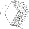
FIG. 1 is a perspective view of a circuit board shield connector according to a first embodiment; -
FIG. 2 is an exploded perspective view of the circuit board shield connector according to the first embodiment; -
FIG. 3 is a perspective view of the circuit board shield connector according to the first embodiment, in which a shield member and an outer housing inFIG. 1 are omitted; -
FIG. 4 is an enlarged view of a major portion ofFIG. 3 ; -
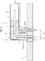
FIG. 5 is a cross-sectional view ofFIG. 3 ; -
FIG. 6 is a perspective view of a circuit board shield connector according to a second embodiment, in which a shield member and an outer housing inFIG. 1 are omitted; -
FIG. 7 is an enlarged view of a major portion ofFIG. 6 ; and -
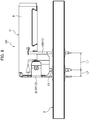
FIG. 8 is a side view ofFIG. 6 . - Various embodiments will be described hereinafter with reference to the accompanying drawings.
- A first embodiment will be described with reference to
FIGS. 1 to 5 . InFIGS. 3 to 5 , ashield member 21 and anouter housing 23 are not illustrated. - A circuit board shield connector 1 according to the present embodiment includes an
inner terminal 7 configured to connect electrically to acircuit board 3 and anouter terminal 11 grounded to thecircuit board 3. Theinner terminal 7 has aconnection part 5 configured to connect electrically to a mating terminal (not illustrated) when the mating terminal is fitted along a planar direction of thecircuit board 3. Theouter terminal 11 has acylindrical part 9 formed in a cylindrical shape. Theouter terminal 11 extends along the planar direction of thecircuit board 3 and covers the outer periphery of theconnection part 5 while being separated from theconnection part 5. Theouter terminal 11 is configured to be grounded to thecircuit board 3 and thecylindrical part 9 is configured to be in contact with a mating shield member (not illustrated) so as to form a shield circuit. - The
inner terminal 7 includes aninner connection part 13. Theinner connection part 13 extends from theconnection part 5 toward thecircuit board 3 side and is configured to connect electrically to thecircuit board 3. Theouter terminal 11 includes a plurality ofouter connection parts 15. The plurality ofouter connection parts 15 extends from thecylindrical part 9 toward thecircuit board 3 side and is configured to be grounded to thecircuit board 3. - With respect to the
inner connection part 13, at least one firstouter connection part 17 included in the plurality ofouter connection parts 15 is at a front side of the otherouter connection parts outer connection parts 15 in the fitting direction of theconnection part 5. On thecircuit board 3, a space L1 between theinner connection part 13 and the firstouter connection part 17 is set wider than a space L2 between theinner connection part 13 and the otherouter connection parts - As illustrated in
FIGS. 1 to 5 , the circuit board shield connector 1 is configured to connect electrically to a device or the like. The circuit board shield connector 1 is configured to mount on thecircuit board 3 as a circuit board on which electronic components (not illustrated) for controlling an operation of the device are mounted. The circuit board shield connector 1 is configured so as a mating connector (not illustrated) to be fitted to the circuit board shield connector 1. The mating connector may be a connector electrically connected to a controller (not illustrated) for controlling the operation of equipment, for example. In the above configuration, an electric signal from the controller is input to thecircuit board 3. The circuit board shield connector 1 includes aninner terminal 7, aninner housing 19, anouter terminal 11, ashield member 21, and anouter housing 23. - The
inner terminal 7 is made of a conductive material. As illustrated inFIGS. 2 and5 , theinner terminal 7 includes aconnection part 5, aninner connection part 13, and press-fit parts 25. - The
connection part 5 is formed in a rod shape and extended along the planar direction of thecircuit board 3. In a state that the mating connector is fitted to the circuit board shield connector 1, theconnection part 5 is configured to fit to a mating terminal (not illustrated) having a box-shaped connection part accommodated in the mating connector. Theconnection part 5 is fitted to the mating terminal along the planar direction of thecircuit board 3. Theinner terminal 7 and the mating terminal are electrically connected by fitting theconnection part 5 into the mating terminal. - The
inner connection part 13 is formed of a single member being continuous with theconnection part 5. Theinner connection part 13 is extended in a direction orthogonal to the fitting direction of theconnection part 5 by bending one end of theconnection part 5 toward thecircuit board 3 side. Theinner connection part 13 is electrically connected to a conductive pattern formed on thecircuit board 3 by soldering. Accordingly, theinner terminal 7 is electrically connected to thecircuit board 3. - The press-
fit parts 25 are formed of a single member being continuous with theconnection part 5 on theinner connection part 13 side of theconnection part 5. The press-fit parts 25 are provided in a protruding manner on both sides of theconnection part 5 in the width direction along a longitudinal direction of theconnection part 5. The press-fit parts 25 are press-fitted into an inner wall surface of theinner housing 19. Accordingly, theinner terminal 7 is fixed to theinner housing 19. - The
inner housing 19 is made of an insulating material such as synthetic resin. As illustrated inFIGS. 2 and5 , a plurality of theinner housings 19 are mounted on thecircuit board 3 so as each of a plurality ofinner terminals 7 is capable of being accommodated in eachinner housing 19. Theinner housing 19 is formed in a cylindrical shape and configured to accommodate theconnection part 5 of theinner terminal 7. In such aninner housing 19, the press-fit part 25 of theinner terminal 7 is press-fitted into the inner wall surface of theinner housing 19, and theinner terminal 7 is fixed to theinner housing 19 so as to accommodate theconnection portion 5 of theinner terminal 7. Theinner housing 19 is accommodated in theouter terminal 11. At this time, theinner housing 19 retains insulation between theinner terminal 7 and theouter terminal 11. - The
outer terminal 11 is made of a conductive material. As illustrated inFIGS. 2 to 5 , each of a plurality of theouter terminals 11 accommodates each of the plurality ofinner housings 19. Theouter terminal 11 includes acylindrical part 9 and a plurality ofouter connection parts 15. - The
cylindrical part 9 is formed in a cylindrical shape and extends along the planar direction of thecircuit board 3 so as to accommodate theinner housing 19. In a state where the circuit board shield connector 1 and the mating connector are fitted to each other, thecylindrical part 9 is brought into contact with a mating shield member (not illustrated) housed in the mating connector in a state and form a shield circuit with the mating shield member. By forming the shield circuit, entering of noise to theinner terminal 7 from the outside or leakage of noise from theinner terminal 7 can be prevented. - Each of the plurality of
outer connection parts 15 is formed of a single member being continuous with thecylindrical part 9. Eachouter connection part 15 extends from thecylindrical portion 9 toward thecircuit board 3 side in a direction orthogonal to the fitting direction of the circuit board shield connector 1 and the mating connector. The plurality ofouter connection parts 15 is electrically connected to a ground pattern formed on thecircuit board 3 by soldering. Accordingly, theouter terminal 11 is grounded to thecircuit board 3. Theouter terminal 11 is accommodated in theshield member 21 and theouter housing 23. - The
shield member 21 is made of a conductive material formed by die casting. As illustrated inFIGS. 1 and2 , theshield member 21 is provided with a plurality ofaccommodating recesses 27 formed to accommodate each of a plurality ofouter terminals 11 to respective accommodating recesses 27. The inner peripheral surface of the plurality ofaccommodating recesses 27 is in contact with the outer peripheral surface of theouter terminal 11 and theouter terminal 11 and theshield member 21 are electrically connected to each other. Theshield member 21 has a plurality ofprotrusions 29. Theshield member 21 is grounded to thecircuit board 3 by inserting the plurality ofprotrusions 29 intoholes 3a formed in thecircuit board 3 and electrically connecting the plurality ofprotrusions 29 to the ground pattern by soldering. Theshield member 21 is accommodated in theouter housing 23. - The
outer housing 23 is made of an insulating material such as synthetic resin. As illustrated inFIGS. 1 and2 , theouter housing 23 is formed in a frame shape and is configured to accommodate theshield member 21 and theouter terminal 21 accommodated in theshield member 21. On both sides of theouter housing 23, metal pegs 31 are fixed by fixing means such as press-fitting. Thepegs 31 are provided with a plurality of fixingparts 33 configured to be fixed to thecircuit board 3 by soldering. Theouter housing 23 is configured to be fixed onto thecircuit board 3 through thepegs 31. A mating connector is fitted to theouter housing 23 along the planar direction of thecircuit board 3. - In the circuit board shield connector 1, while the mating connector is fitted, the
inner terminal 7 is electrically connected to the mating terminal. Thus, an electric signal from the controller can be inputted to thecircuit board 3. At this time, theouter terminal 11 is electrically connected to the mating shield member and forms a shield circuit. Thus, theinner terminal 7 is protected from external noise. - In such a circuit board shielded connector 1, conduction noise may be transmitted from the mating shield member to the
outer terminal 11 while the mating connector is fitted to the circuit board shield connector 1. At this time, the conduction noise transmits through thecylindrical part 9 of theouter terminal 11 and is grounded to thecircuit board 3 via the plurality ofouter connection parts 15 of theouter terminal 11. When the conduction noise flows on thecircuit board 3 in the vicinity of theinner connection part 13 of theinner terminal 7, the electric signal may be disturbed, and the device or the like electrically connected to thecircuit board 3 may malfunction. - Therefore, in the circuit board shielded connector 1, at least one of the plurality of
outer connection parts 15, the firstouter connection part 17, is disposed in front of theinner connection part 13 in the fitting direction of theconnection part 5 with respect to the otherouter connection parts circuit board 3, a space L1 between theinner connection part 13 and the firstouter connection part 17 in the fitting direction of theconnection part 5 is set wider than a space L2 between theinner connection part 13 and the otherouter connection parts - As illustrated in
FIGS. 3 to 5 , the plurality ofouter connection parts 15 include the firstouter connection part 17, a secondouter connection part 35, and a thirdouter connection part 37. The firstouter connection part 17 is arranged at the front side in the fitting direction between theconnection part 5 and the mating terminal of the secondouter connection part 35 and the thirdouter connection part 37 with respect to theinner connection part 13. Therefore, as indicated by an arrow illustrated inFIG. 5 , the conduction noise transmitted from the mating shield member to thecylindrical part 9 flows from the firstouter connection part 17 to thecircuit board 3 prior to the secondouter connection part 35 and the thirdouter connection part 37. - The space L1 between the first
outer connection part 17 through which conduction noise flows first and theinner connection part 13 is set wider than the space L2 between the secondouter connection part 35 or the thirdouter connection part 37 and theinner connection part 13. Therefore, on thecircuit board 3, the conduction noise that flow through the firstouter connection part 17 before flowing through the secondouter connection part 35 or the thirdouter connection part 37 does not flow near theinner connection part 13. Therefore, on thecircuit board 3, the conduction noise that flow near theinner connection part 13 can be reduced, and the influence of the conduction noise to the electric signal flowing through theinner connection part 13 can be suppressed. Therefore, the disturbance of the electric signal is reduced, and the stable electric signal can be input to thecircuit board 3 electrically connected to the device or the like. - In such a circuit board shielded connector 1, the first
outer connection part 17 is arranged at the front side in the fitting direction of theconnection part 5 of the otherouter connection parts inner connection part 13. Therefore, the conduction noise transmitted from the mating shield member can be made to flow to thecircuit board 3 from the firstouter connection part 17 prior to the otherouter connection parts - On the
circuit board 3, the space L1 between theinner connection part 13 and the firstouter connection part 17 is set wider than the space L2 between theinner connection part 13 and the otherouter connection parts circuit board 3, the conduction noise that flow through the firstouter connection part 17 prior to the otherouter connection parts inner connection part 13. - Therefore, in the circuit board shield connector 1, the conduction noise that flow near the
inner connection part 13 can be reduced, and the influence to theinner terminal 7 by the conduction noise that flow through theouter terminal 11 can be effectively suppressed. - A second embodiment will be described with reference to
FIGS. 6 to 8 . InFIGS. 6 to 8 , theshield member 21 and theouter housing 23 in the first embodiment that may be also included in the second embodiment are omitted in the drawings. - In the circuit
board shield connector 101 according to the present embodiment, thecylindrical portion 9 and the firstouter connection part 103 are formed as separate bodies. - It should be noted that, in the same configuration as that of the first embodiment, the same symbols are used to refer to the first embodiment and a description of the configuration and the function is omitted. In the same configuration as that of the first embodiment, the effects obtained are the same.
- As illustrated in
FIGS. 6 to 8 , the firstouter connection part 103 is formed as a separate body from thecylindrical part 9. The firstouter connection part 103 is fixed to the outer periphery of thecylindrical part 9 at an arbitrary position by, for example, an engaging means engaged with each other or a fixing means such as welding, and is electrically connected to thecylindrical part 9. The firstouter connection part 103 is electrically connected to a ground pattern formed on thecircuit board 3 by soldering. Thus, theouter terminal 11 is grounded to thecircuit board 3. - In the circuit
board shield connector 101, since thecylindrical part 9 and the firstouter connection part 103 are formed as separately bodies, the firstouter connection part 103 can be selectively assembled to thecylindrical part 9 at an arbitrary position. Therefore, the space L1 between theinner connection part 13 and the firstouter connection part 103 can be easily adjusted, and the degree of freedom in design can be improved. - Although the present embodiments have been described above, the present embodiments are not limited thereto, and various modifications can be made within the scope of the gist of the present embodiments.
- For example, in the embodiments, a plurality of outer connection parts are provided at three locations. However, the plurality of outer connection parts are not limited to this, and two outer connection parts or four or more outer connection parts may be provided.
- Further, two or more outer connection parts may be arranged at the front side of the other outer connection parts in the fitting direction of the connection part with respect to the inner connection part.
- Further, the outer connection part disposed at the rear side in the fitting direction of the connection part may be formed as a separate body from the cylindrical part.
- Further, although the inner connection part and the outer connection part are electrically connected to the circuit board by soldering, the present invention is not limited thereto, and the inner connection part and the outer connection part may be electrically connected to the circuit board by a press fit or the like.
- Although the present invention has been described above by reference to the embodiments, the present invention is not limited to those and the configuration of parts can be replaced with any configuration having a similar function, as long as they lie within the scope of the claims.
Claims (2)
- A circuit board shield connector comprising:an inner terminal having a connection part configured to connect electrically to a circuit board and to connect electrically to a mating terminal by fitting the mating terminal along a planar direction of the circuit board; andan outer terminal having a cylindrical part, the cylindrical part formed in a cylindrical shape and configured to extend along the planar direction of the circuit board and covering the outer periphery of the connection part while being separated from the connection part and configured to contact with a mating shield member to form a shield circuit, and configured to be grounded to the circuit board, whereinthe inner terminal comprises an inner connection part, the inner connection part extending from the connection part toward the circuit board side and configured to connect electrically to the circuit board,the outer terminal comprises a plurality of outer connection parts, the plurality of outer connection parts extending from the cylindrical part toward the circuit board side and configured to be grounded to the circuit board,with respect to the inner connection part, at least one first outer connection part included in the plurality of outer connection parts is on a front side of the other outer connection part of the plurality of outer connection parts in a fitting direction of the connection part,on the circuit board, a space between the inner connection part and the first outer connection part is set wider than a space between the inner connection part and the other outer connection part.
- The circuit board shield connector according to claim 1, wherein the cylindrical part and the first outer connection part are formed as separate bodies.
Applications Claiming Priority (1)
| Application Number | Priority Date | Filing Date | Title |
|---|---|---|---|
| JP2020000274A JP2021111439A (en) | 2020-01-06 | 2020-01-06 | Shielded connector for board |
Publications (1)
| Publication Number | Publication Date |
|---|---|
| EP3846293A1 true EP3846293A1 (en) | 2021-07-07 |
Family
ID=74003741
Family Applications (1)
| Application Number | Title | Priority Date | Filing Date |
|---|---|---|---|
| EP20217571.7A Withdrawn EP3846293A1 (en) | 2020-01-06 | 2020-12-29 | Circuit board shield connector |
Country Status (4)
| Country | Link |
|---|---|
| US (1) | US20210210909A1 (en) |
| EP (1) | EP3846293A1 (en) |
| JP (1) | JP2021111439A (en) |
| CN (1) | CN113078520A (en) |
Families Citing this family (1)
| Publication number | Priority date | Publication date | Assignee | Title |
|---|---|---|---|---|
| JP7461394B2 (en) * | 2022-01-31 | 2024-04-03 | 住友電装株式会社 | shield connector |
Citations (4)
| Publication number | Priority date | Publication date | Assignee | Title |
|---|---|---|---|---|
| US5334050A (en) * | 1992-02-14 | 1994-08-02 | Derek Andrews | Coaxial connector module for mounting on a printed circuit board |
| JP2002270311A (en) * | 2000-08-30 | 2002-09-20 | Molex Inc | Electric connector for a coaxial cable and its manufacturing method |
| US20050221673A1 (en) * | 2004-03-31 | 2005-10-06 | Myer John M | Shielded electrical jack connector |
| JP2013048048A (en) | 2011-08-29 | 2013-03-07 | Sumitomo Wiring Syst Ltd | connector |
Family Cites Families (3)
| Publication number | Priority date | Publication date | Assignee | Title |
|---|---|---|---|---|
| JP4194555B2 (en) * | 2004-04-28 | 2008-12-10 | ヒロセ電機株式会社 | Coaxial connector |
| JP2008084561A (en) * | 2006-09-26 | 2008-04-10 | Auto Network Gijutsu Kenkyusho:Kk | Board shield connector connection structure |
| JP6879648B2 (en) * | 2019-02-27 | 2021-06-02 | 住友電装株式会社 | Outer conductor terminal and shield connector |
-
2020
- 2020-01-06 JP JP2020000274A patent/JP2021111439A/en not_active Abandoned
- 2020-12-29 EP EP20217571.7A patent/EP3846293A1/en not_active Withdrawn
-
2021
- 2021-01-04 US US17/140,571 patent/US20210210909A1/en not_active Abandoned
- 2021-01-05 CN CN202110008806.5A patent/CN113078520A/en not_active Withdrawn
Patent Citations (4)
| Publication number | Priority date | Publication date | Assignee | Title |
|---|---|---|---|---|
| US5334050A (en) * | 1992-02-14 | 1994-08-02 | Derek Andrews | Coaxial connector module for mounting on a printed circuit board |
| JP2002270311A (en) * | 2000-08-30 | 2002-09-20 | Molex Inc | Electric connector for a coaxial cable and its manufacturing method |
| US20050221673A1 (en) * | 2004-03-31 | 2005-10-06 | Myer John M | Shielded electrical jack connector |
| JP2013048048A (en) | 2011-08-29 | 2013-03-07 | Sumitomo Wiring Syst Ltd | connector |
Also Published As
| Publication number | Publication date |
|---|---|
| US20210210909A1 (en) | 2021-07-08 |
| CN113078520A (en) | 2021-07-06 |
| JP2021111439A (en) | 2021-08-02 |
Similar Documents
| Publication | Publication Date | Title |
|---|---|---|
| US7815467B2 (en) | Connector device | |
| JP5221188B2 (en) | Shield connector | |
| US6908339B2 (en) | Connector having a simple structure assuring a stable mounting operation | |
| US10403995B2 (en) | Electrical connector, electronic component, and assembly method | |
| KR20090050005A (en) | PCB Assembly | |
| US10170868B1 (en) | Connector | |
| KR20170036529A (en) | Board to board connector and rf connector integral connector assembly | |
| JP7606661B2 (en) | PCB Connectors and Devices | |
| JP7713162B2 (en) | PCB Connectors and Devices | |
| JP2019140014A (en) | Electrical connector | |
| US20150017836A1 (en) | Active plug connector and method for assembling the same | |
| JP6211030B2 (en) | Electronic control device and method of manufacturing electronic control device | |
| US12136778B2 (en) | Connector, connector module, and electronic apparatus | |
| US20210210909A1 (en) | Circuit board shield connector | |
| US7367818B2 (en) | Onboard connector | |
| US9515422B2 (en) | Electrical connector having an integrated impedance equalisation element | |
| JP2013089342A (en) | Connector device | |
| CN112470344B (en) | Edge connectors and printed circuit board assemblies | |
| CN112615177B (en) | Connector and electronic device | |
| JP6319657B2 (en) | Shield connector | |
| US11329415B2 (en) | Connection structure for circuit board and board connector, and board connector | |
| US8632361B2 (en) | Electrical connector | |
| KR102921737B1 (en) | Connectors and Connector Systems | |
| JP7363228B2 (en) | Connector devices, connectors, and connector structures | |
| JP6010819B2 (en) | Connector board fixing structure |
Legal Events
| Date | Code | Title | Description |
|---|---|---|---|
| STAA | Information on the status of an ep patent application or granted ep patent |
Free format text: STATUS: REQUEST FOR EXAMINATION WAS MADE |
|
| PUAI | Public reference made under article 153(3) epc to a published international application that has entered the european phase |
Free format text: ORIGINAL CODE: 0009012 |
|
| 17P | Request for examination filed |
Effective date: 20201229 |
|
| AK | Designated contracting states |
Kind code of ref document: A1 Designated state(s): AL AT BE BG CH CY CZ DE DK EE ES FI FR GB GR HR HU IE IS IT LI LT LU LV MC MK MT NL NO PL PT RO RS SE SI SK SM TR |
|
| RBV | Designated contracting states (corrected) |
Designated state(s): AL AT BE BG CH CY CZ DE DK EE ES FI FR GB GR HR HU IE IS IT LI LT LU LV MC MK MT NL NO PL PT RO RS SE SI SK SM TR |
|
| STAA | Information on the status of an ep patent application or granted ep patent |
Free format text: STATUS: EXAMINATION IS IN PROGRESS |
|
| 17Q | First examination report despatched |
Effective date: 20211008 |
|
| GRAP | Despatch of communication of intention to grant a patent |
Free format text: ORIGINAL CODE: EPIDOSNIGR1 |
|
| STAA | Information on the status of an ep patent application or granted ep patent |
Free format text: STATUS: GRANT OF PATENT IS INTENDED |
|
| INTG | Intention to grant announced |
Effective date: 20220406 |
|
| STAA | Information on the status of an ep patent application or granted ep patent |
Free format text: STATUS: THE APPLICATION IS DEEMED TO BE WITHDRAWN |
|
| 18D | Application deemed to be withdrawn |
Effective date: 20220817 |