EP3843163A1 - Hall element - Google Patents
Hall element Download PDFInfo
- Publication number
- EP3843163A1 EP3843163A1 EP19853017.2A EP19853017A EP3843163A1 EP 3843163 A1 EP3843163 A1 EP 3843163A1 EP 19853017 A EP19853017 A EP 19853017A EP 3843163 A1 EP3843163 A1 EP 3843163A1
- Authority
- EP
- European Patent Office
- Prior art keywords
- hall
- thin film
- substrate
- magnetic field
- dopant
- Prior art date
- Legal status (The legal status is an assumption and is not a legal conclusion. Google has not performed a legal analysis and makes no representation as to the accuracy of the status listed.)
- Pending
Links
Images







Classifications
-
- G—PHYSICS
- G01—MEASURING; TESTING
- G01R—MEASURING ELECTRIC VARIABLES; MEASURING MAGNETIC VARIABLES
- G01R33/00—Arrangements or instruments for measuring magnetic variables
- G01R33/02—Measuring direction or magnitude of magnetic fields or magnetic flux
- G01R33/06—Measuring direction or magnitude of magnetic fields or magnetic flux using galvano-magnetic devices
- G01R33/07—Hall effect devices
-
- H—ELECTRICITY
- H01—ELECTRIC ELEMENTS
- H01F—MAGNETS; INDUCTANCES; TRANSFORMERS; SELECTION OF MATERIALS FOR THEIR MAGNETIC PROPERTIES
- H01F10/00—Thin magnetic films, e.g. of one-domain structure
- H01F10/08—Thin magnetic films, e.g. of one-domain structure characterised by magnetic layers
- H01F10/10—Thin magnetic films, e.g. of one-domain structure characterised by magnetic layers characterised by the composition
- H01F10/12—Thin magnetic films, e.g. of one-domain structure characterised by magnetic layers characterised by the composition being metals or alloys
- H01F10/14—Thin magnetic films, e.g. of one-domain structure characterised by magnetic layers characterised by the composition being metals or alloys containing iron or nickel
-
- G—PHYSICS
- G01—MEASURING; TESTING
- G01R—MEASURING ELECTRIC VARIABLES; MEASURING MAGNETIC VARIABLES
- G01R33/00—Arrangements or instruments for measuring magnetic variables
- G01R33/02—Measuring direction or magnitude of magnetic fields or magnetic flux
- G01R33/06—Measuring direction or magnitude of magnetic fields or magnetic flux using galvano-magnetic devices
- G01R33/09—Magnetoresistive devices
- G01R33/093—Magnetoresistive devices using multilayer structures, e.g. giant magnetoresistance sensors
-
- H—ELECTRICITY
- H01—ELECTRIC ELEMENTS
- H01F—MAGNETS; INDUCTANCES; TRANSFORMERS; SELECTION OF MATERIALS FOR THEIR MAGNETIC PROPERTIES
- H01F10/00—Thin magnetic films, e.g. of one-domain structure
- H01F10/08—Thin magnetic films, e.g. of one-domain structure characterised by magnetic layers
- H01F10/10—Thin magnetic films, e.g. of one-domain structure characterised by magnetic layers characterised by the composition
- H01F10/12—Thin magnetic films, e.g. of one-domain structure characterised by magnetic layers characterised by the composition being metals or alloys
- H01F10/13—Amorphous metallic alloys, e.g. glassy metals
- H01F10/131—Amorphous metallic alloys, e.g. glassy metals containing iron or nickel
-
- H—ELECTRICITY
- H10—SEMICONDUCTOR DEVICES; ELECTRIC SOLID-STATE DEVICES NOT OTHERWISE PROVIDED FOR
- H10N—ELECTRIC SOLID-STATE DEVICES NOT OTHERWISE PROVIDED FOR
- H10N50/00—Galvanomagnetic devices
- H10N50/10—Magnetoresistive devices
-
- H—ELECTRICITY
- H10—SEMICONDUCTOR DEVICES; ELECTRIC SOLID-STATE DEVICES NOT OTHERWISE PROVIDED FOR
- H10N—ELECTRIC SOLID-STATE DEVICES NOT OTHERWISE PROVIDED FOR
- H10N52/00—Hall-effect devices
-
- H—ELECTRICITY
- H10—SEMICONDUCTOR DEVICES; ELECTRIC SOLID-STATE DEVICES NOT OTHERWISE PROVIDED FOR
- H10N—ELECTRIC SOLID-STATE DEVICES NOT OTHERWISE PROVIDED FOR
- H10N52/00—Hall-effect devices
- H10N52/101—Semiconductor Hall-effect devices
-
- H—ELECTRICITY
- H10—SEMICONDUCTOR DEVICES; ELECTRIC SOLID-STATE DEVICES NOT OTHERWISE PROVIDED FOR
- H10N—ELECTRIC SOLID-STATE DEVICES NOT OTHERWISE PROVIDED FOR
- H10N52/00—Hall-effect devices
- H10N52/80—Constructional details
-
- H—ELECTRICITY
- H10—SEMICONDUCTOR DEVICES; ELECTRIC SOLID-STATE DEVICES NOT OTHERWISE PROVIDED FOR
- H10N—ELECTRIC SOLID-STATE DEVICES NOT OTHERWISE PROVIDED FOR
- H10N52/00—Hall-effect devices
- H10N52/80—Constructional details
- H10N52/85—Materials of the active region
Definitions
- the present invention relates to a Hall element.
- a non-contact magnetic sensor uses the Hall effect to detect a magnetic field induced by an electric current, an earth's magnetic field, or a small magnetic field from a biological body, convert the detected magnetic field into an electrical signal, and output the electrical signal.
- a magnetic sensor is called a Hall element (refer to Patent Literature 1 and Patent Literature 2, for example).
- the Hall element is built in an electronic device such as a mobile phone, a notebook PC, and a digital camera. In recent years, there is a growing demand for Hall elements.
- the conventional high-sensitive Hall elements are made of a material such as GaAs, InAs, or InSb, containing toxic arsenic (As) or rare metal indium (In), which requires a careful handling.
- the conventional Hall elements use the above-mentioned ordinary Hall effect derived from the Lorentz force to detect magnetic fields.
- the implementation of high mobility materials is essential by controlling crystalline quality or purity of a sample, which imposes a limitation on a sample fabrication method to satisfy such conditions. Specifically, it is necessary to integrate a single-crystalline thin film onto a single-crystalline substrate at high temperature, which leads to higher costs and makes it difficult to add mechanical flexibility to the Hall element.
- the temperature dependence of the device characteristics is degraded. That is, there is a trade-off relationship between the sensitivity and temperature stability and thus, an IC is required to compensate a sensitivity variation.
- Non Patent Literature 1 E. Haftek, M. Tan, J.A. Barnard, "Microstructure and magnetic properties of ferromagnetic Fe-Sn alloy thin films,” Ultramicroscopy 47 p.400-p.407 (1992 ).
- Non Patent Literature 2 Jun Gao, Fei Wang, Xiaolong Jiang, Gang Ni, Fengming Zhang, and Youwei Du, "Giant Hall effect in FexSn100-x granular alloy films, "Journal of Applied Physics 93, 1851 (2003 ).
- the invention has been made in view of the foregoing, and an object of the invention is to provide a Hall element containing a new composition material that exhibits the anomalous Hall effect.
- a Hall element exhibits an anomalous Hall effect, and includes a substrate and a thin film as a magneto-sensitive layer on the substrate, the thin film having a composition of Fe x Sn 1-x , where 0.5 ⁇ x ⁇ 0.9.
- a Hall element exhibits an anomalous Hall effect, and includes a substrate and a thin film as a magneto-sensitive layer on the substrate.
- the thin film is made of an alloy of Fe and Sn, and a dopant element, and the dopant element is a transition metal element that modulates spin-orbit coupling or magnetism.
- a Hall element exhibits an anomalous Hall effect, and includes a substrate and a thin film as a magneto-sensitive layer on the substrate.
- the thin film is made of an alloy of Fe and Sn, and a dopant element, and the dopant element is a main-group element that has a different number of valence electrons from Sn and modulates carrier density.
- a Hall element exhibits an anomalous Hall effect, and includes a substrate and a thin film as a magneto-sensitive layer on the substrate.
- the thin film is made of an alloy of Fe and Sn, and a dopant element, and the dopant element is a main-group element that modulates density of states.
- a Hall element that contains a non-toxic and inexpensive material, can be fabricated by a general-purpose technique, can also be fabricated on a flexible substrate, and is excellent in properties such as temperature stability.
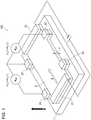
- the Hall element 100 includes a substrate 1, and a thin film 2 as a magneto-sensitive layer on the substrate 1.
- the thin film 2 contains an alloy of Fe and Sn.
- Examples of the material of the substrate 1 include, but are not limited to, polyethylene naphthalate (PEN), polyethylene terephthalate (PET), polyimide, glass, sapphire (single-crystalline Al 2 O 3 ), alumina (Al 2 O 3 ceramic), magnesium oxide (MgO), strontium titanate (SrTiO 3 ), quartz (SiO 2 ), silicon (Si), gallium arsenide (GaAs), or indium phosphide (InP) .
- PEN polyethylene naphthalate
- PET polyethylene terephthalate
- polyimide glass
- sapphire single-crystalline Al 2 O 3
- Al 2 O 3 ceramic alumina
- MgO magnesium oxide
- strontium titanate SrTiO 3
- quartz SiO 2
- silicon Si
- GaAs gallium arsenide
- InP indium phosphide
- the thin film 2 has a Hall-bar structure with six terminals 21 to 26.
- a thickness of the thin film 2 is denoted by d
- a distance between the terminals 23 and 24 is denoted by L
- a width of the thin film 2 is denoted by W.
- a four-terminal, cross-shaped Hall-bar structure may be employed.
- Example 1 in which the thin film 2 is made of an Fe-Sn alloy
- Example 2 and Example 3 in which the thin film 2 is made of a ternary compound of an Fe-Sn alloy and a dopant element (impurities).
- Example 1 demonstrates the thin film 2 made of an Fe x Sn 1-x alloy.
- a Fe x Sn 1-x film is prepared by radio-frequency (RF) magnetron sputtering, for example.
- RF radio-frequency
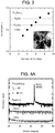
- Fe chips are placed on an Sn target, and an Fe content x in the Fe x Sn 1-x film is controlled by changing the number of Fe chips on the Sn target.
- a white scale bar represents 10 mm.
- Fig. 3 shows a relationship between the number of Fe chips and the Fe content x.
- the sputtering as described above is an industrially general-purpose technique, and makes it possible to prepare a highly-uniform thin film and easily spread the thin film over a large area.
- Alternative techniques for attaining a similar composition of Fe and Sn may include the use of an alloy target in which the composition of Fe and Sn is tuned, or supplying Fe and Sn from different sputtering sources to tune the composition of the thin film. Any of these techniques may be employed.
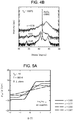
- Fig. 4A indicates that the room-temperature grown samples do not have crystalline character and are expected to have excellent uniformity.
- the film thicknesses d are approximately 40 nm.
- Fig. 4B indicates that a crystalline sample can be also prepared by high-temperature growth.
- the electrical transport properties are measured using VersaLab (Quantum Design), a physical property measurement system (Quantum Design), and a power-supply measurement unit.
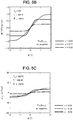
- the behavior of the Hall resistivity ⁇ yx is remarkably similar to magnetization curves, indicating that the response of the Hall resistivity ⁇ yx results from the anomalous Hall effect, and an anomalous Hall effect contribution is dominant over an ordinary Hall effect contribution.
- ⁇ xx is longitudinal resistivity.
- the inset of Fig. 5E shows the longitudinal resistivity ⁇ xx (triangles) and the Hall resistivity ⁇ yx (squares) for the non-crystalline Fe x Sn 1-x films.
- ⁇ yx / ⁇ xx of the crystalline films shows a similar behavior, but is smaller than ⁇ yx / ⁇ xx of the non-crystalline films.
- ⁇ xy ⁇ yx/ ( ⁇ xx 2 + ⁇ yx 2 ) for non-crystalline Fe 0.60 Sn 0.40 films (filled circles) and crystalline Fe 0.62 Sn 0.38 films (open circles).
- data plots (squares) of bulk Fe 3 Sn 2 single crystals described in the following literature are also included: Ye, L. et al. "Massive Dirac fermions in a ferromagnetic kagome metal," Nature 555, 638-642 (2018 ).
- T g 500°C
- V yx ⁇ W L BV in
- ⁇ is a mobility
- V in is an input voltage for allowing an electric current to flow (the longitudinal voltage V xx shown in Fig. 1 and Fig. 2 ).
- the Hall voltage V yx is determined by the mobility ⁇ except for the magnetic field B and a geometrical factor W/L, and the sensitivity can be obtained from the mobility ⁇ .
- I in represents an electric current (the electric current I shown in Fig. 1 and Fig. 2 )
- the Hall resistivity ⁇ yx is a function of the magnetic field B. From Equation (2), the sensitivity of the Hall element 100 can be obtained from d ⁇ yx /dB and ⁇ yx / ⁇ xx .
- the temperature stability of the mobility ⁇ and that of ⁇ yx / ⁇ xx are used as their indexes, respectively.
- the temperature stability in this ⁇ yx / ⁇ xx term is high, and thus, the temperature stability of the Hall element 100 of the embodiments is more excellent than that of the ordinary semiconductor Hall element.
- Sensitivity Coefficient V yx BV in mV / mT / V
- This value of the sensitivity coefficient is approximately 1/3 of a sensitivity coefficient of GaAs 650 Ohm element, which is approximately 0.25 mV/mT/V representing a standard sensitivity, and is expected to increase by tuning the configuration, the composition, or the like (refer to Pham Nam hai, "Super-high-sensitivity anomalous Hall effect magnetic sensor," New Technology Presentation Meetings! ).
- the graphs a of Fig. 6 clearly demonstrate that the anomalous Hall effects on those three substrates are essentially the same, meaning that no specific substrate is required in order to attain a giant anomalous Hall effect.
- Each inset in the graphs b of Fig. 6 shows contour plots of the magnetic sensitivity ⁇ against the temperature T and the magnetic field B.
- the graphs b of Fig. 6 indicate that the magnetic sensitivity ⁇ is almost constant at a high magnetic field and is rarely affected by a temperature change. This is also obvious from a variation of the magnetic sensitivity ⁇ as described below.
- a change in the longitudinal resistivity ⁇ xx with respect to the temperature T is extremely small on any of the substrates . This indicates that the Hall element 100 of the embodiments has an advantage over semiconductor devices with thermally activated transport properties.
- Fig. 8B shows film thickness dependence of the longitudinal resistivity ⁇ xx and ⁇ yx / ⁇ xx for the Fe 0.60 Sn 0.40 films.
- ⁇ yx / ⁇ xx can be maintained at 0.04 to 0.05, and a giant anomalous Hall effect occurs.
- Fig. 8B indicates that ⁇ yx / ⁇ xx is maintained at approximately a constant value with the film thickness d of 20 nm or more, implying almost no film thickness dependence.
- the longitudinal resistivity ⁇ xx rapidly increases, and ⁇ yx / ⁇ xx rapidly decreases.
- the change of the width W and/or the length L other than the film thickness d to fabricate a new Hall element may lead to the enhancement of the anomalous Hall effect.
- Fig. 9A and Fig. 9B two types of devices (an x-bent device and a y-bent device), each attached to a surface of a semicircular jig with a radius of 4.9 mm, are prepared.
- the x-bent device shown in Fig. 9A is attached to the semicircular jig such that the direction of the electric current I is parallel to a circumferential direction of the semicircular jig.
- the y-bent device shown in Fig. 9B is attached to the semicircular jig such that the direction of the electric current I is parallel to an axial direction of the semicircular jig.
- Fig. 10A shows magnetic field dependence of the Hall resistance R yx for a Hall element in a flat state and Hall elements in bent states (that is, the x-bent device and the y-bent device), and Fig. 10B shows magnetic field dependence of sheet resistance R sheet for such Hall elements.
- Example 1 providing the Hall element 100 including the thin film 2 made of a non-toxic and inexpensive alloy of Fe and Sn (Fe x Sn 1-x (0.5 ⁇ x ⁇ 0.9)) enables stability in a wide range of temperature including a room temperature, and detection of the Hall voltage as with the conventional semiconductors.
- the material of the substrate 1 is not particularly limited, unlike substrates used in the conventional Hall elements, such as a GaAs single-crystalline substrate.
- a flexible substrate can also be employed. This makes it possible to achieve a small and lightweight Hall element 100.
- Example 2 demonstrates the anomalous Hall effect when the thin film 2 is a ternary compound containing an Fe-Sn alloy and a dopant element (impurity), and the dopant element is a transition metal element that is added in order to modulate spin-orbit coupling or magnetism.
- Example 2 the thin film 2 containing a ternary compound is provided on the sapphire substrate 1.
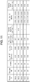
- Fig. 11 shows properties of an Fe-Sn alloy as a non-doped reference sample that is used in the measurement of an impurity doping effect or comparative verification.
- the composition ratio represents the results from energy dispersive X-ray spectrometry (EDX).
- EDX energy dispersive X-ray spectrometry
- Example 2 experiments of adding each of tantalum (Ta), tungsten (W), molybdenum (Mo), platinum (Pt), and manganese (Mn) to a non-doped reference sample N2 are performed by room-temperature sputtering.
- the addition of Ta, the addition of W, the addition of Mo, and the addition of Pt are mainly aimed at modulating spin-orbit coupling, and the addition of Mn is mainly aimed at modulating magnetism.
- Example 2 let us suppose that an Fe site of the non-doped reference sample N2 is substituted with a dopant X, and a doping level representing a doping rate is defined as X/(Fe + X).
- Fig. 12A shows experimental results of adding Ta to the non-doped reference sample N2
- Fig. 12B shows experimental results of adding W to the non-doped reference sample N2, adding Mo to the non-doped reference sample N2, adding Pt to the non-doped reference sample N2, and adding Mn to the non-doped reference sample N2.
- Fig. 12A nine sample IDs of the dopant Ta are denoted by T1 to T9 in ascending order of the doping level.
- Fig. 12B two sample IDs of the dopant W are denoted by W1 and W2 in ascending order of the doping level, a sample ID of the dopant Mo is denoted by O1, a sample ID of the dopant Pt is denoted by P1, and a sample ID of the dopant Mn is denoted by M1.
- the Hall resistivity ⁇ yx of the samples T1 and T3 to T6 is higher than that of the non-doped reference sample N2, and the magnetic sensitivity d ⁇ yx /dB of the samples T2 to T7 is higher than that of the non-doped reference sample N2.
- ⁇ yx / ⁇ xx of the samples T1 and T4 is higher than that of the non-doped reference sample N2.
- the magnetic sensitivity d ⁇ yx /dB of the samples W1, W2, and O1 is higher than that of the non-doped reference sample N2.
- the magnetic sensitivity d ⁇ yx /dB at a low magnetic field (B ⁇ 0.2T) is extremely high compared to the non-doped reference sample N2.
- both of the Hall resistivity ⁇ yx and the magnetic sensitivity d ⁇ yx /dB are the highest, and the magnetic sensitivity d ⁇ yx /dB (29.1 ⁇ cm/T) even approaches twice that of the non-doped reference sample N2.
- Fig. 13B to Fig. 13D and Fig. 14 suggest that the saturation magnetic field B sat (a maximum detectable magnetic field) of the samples T5, T6, and T7 is slightly less than that of the non-doped reference sample N2, but is maintained at approximately 0.2T to 0.4T.
- ⁇ yx / ⁇ xx rarely depends on the film thickness d at the film thickness of 20 nm or more.
- the film thicknesses d of all of the samples T1 to T9, W1, W2, O1, P1, and M1 are in a range of 35 nm to 65 nm, which is sufficiently greater than 20 nm.
- Example 3 demonstrates the anomalous Hall effect when the thin film 2 is a ternary compound containing an Fe-Sn alloy and a dopant element (impurity), and the dopant element is a main-group element that is added in order to modulate carrier density or density of states.
- Example 3 the thin film 2 containing a ternary compound is provided on the sapphire substrate 1.
- Example 3 experiments of adding each of indium (In) and germanium (Ge) to the non-doped reference sample N2 are performed by room-temperature sputtering.
- the experimental conditions are the same as those of Example 2.
- the addition of In having a different number of valence electrons from that of Sn is aimed at modulating carrier density, and the addition of Ge is mainly aimed at modulating density of states.
- Example 3 let us suppose that an Sn site of the non-doped reference sample N2 is substituted with a dopant X, and a doping level representing a doping rate is defined as X/(Sn + X).
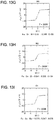
- Fig. 15 shows experimental results of adding In to the non-doped reference sample N2 and adding Ge to the non-doped reference sample N2.
- Fig. 15 two sample IDs of the dopant In are denoted by I1 and I2 in ascending order of the doping level, and a sample ID of the dopant Ge is denoted by G1.
- the Hall resistivity ⁇ yx of the sample I1 is higher than that of the non-doped reference sample N2, and ⁇ yx / ⁇ xx of the samples I1 and I2 is higher than that of the non-doped reference sample N2. This indicates that a giant anomalous Hall effect occurs in the samples I1 and I2.
- the film thicknesses d of all of the samples I1, I2, and G1 are sufficiently greater than 20 nm. Accordingly, a change in various parameters such as the Hall resistivity ⁇ yx , ⁇ yx / ⁇ xx , and the magnetic sensitivity d ⁇ yx /dB rarely depends on the film thickness d, and the improvement of the properties of the samples in Example 3 is attributed to impurity doping.
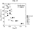
- Fig. 17 shows a relationship between the saturation magnetic field B sat and the magnetic sensitivity d ⁇ yx /dB for the ternary compounds and the non-doped reference samples N1 to N5 according to Example 2 and Example 3.
- a heavy transition metal element such as Ta or W has a strong spin-orbit coupling, and the spin-orbit coupling can be increased by adding such a heavy transition metal element to the Fe-Sn alloy.
- Example 2 and Example 3 The experimental conditions for adding the impurity described in Example 2 and Example 3 are presented for the purposes of illustration and not limitation.
- the impurity may be added by a method other than sputtering.
- a plurality of impurities may be added.
- the thin film may be provided on a substrate made of a material other than sapphire.
- Sb is added as a main-group element having a different number of valence electrons from that of Sn to modulate carrier density, the anomalous Hall effect may occur.
Landscapes
- Physics & Mathematics (AREA)
- Condensed Matter Physics & Semiconductors (AREA)
- General Physics & Mathematics (AREA)
- Engineering & Computer Science (AREA)
- Power Engineering (AREA)
- Hall/Mr Elements (AREA)
- Measuring Magnetic Variables (AREA)
- Thin Magnetic Films (AREA)
Abstract
Description
- The present invention relates to a Hall element.
- When a magnetic field is applied to a substance perpendicularly to an electric current flowing in the substance, an electromotive force is generated in a direction transverse to both the electric current and the magnetic field. This phenomenon is called the Hall effect. A non-contact magnetic sensor uses the Hall effect to detect a magnetic field induced by an electric current, an earth's magnetic field, or a small magnetic field from a biological body, convert the detected magnetic field into an electrical signal, and output the electrical signal. Such a magnetic sensor is called a Hall element (refer to
Patent Literature 1 andPatent Literature 2, for example). The Hall element is built in an electronic device such as a mobile phone, a notebook PC, and a digital camera. In recent years, there is a growing demand for Hall elements. - However, the conventional high-sensitive Hall elements are made of a material such as GaAs, InAs, or InSb, containing toxic arsenic (As) or rare metal indium (In), which requires a careful handling. The conventional Hall elements use the above-mentioned ordinary Hall effect derived from the Lorentz force to detect magnetic fields. In addition, as shown in a sensitivity index described below, the implementation of high mobility materials is essential by controlling crystalline quality or purity of a sample, which imposes a limitation on a sample fabrication method to satisfy such conditions. Specifically, it is necessary to integrate a single-crystalline thin film onto a single-crystalline substrate at high temperature, which leads to higher costs and makes it difficult to add mechanical flexibility to the Hall element. Further, as sensitivity of the Hall element increases, the temperature dependence of the device characteristics is degraded. That is, there is a trade-off relationship between the sensitivity and temperature stability and thus, an IC is required to compensate a sensitivity variation.
- Meanwhile, thin films made of iron (Fe) and tin (Sn) that are inexpensive and easily available have been characterized, and the Hall effect of an Fe-Sn alloy has been studied (refer to
Non Patent Literature 1 and Non Patent Literature 2). -
- Patent Literature 1:
Japanese Laid-Open Patent Publication No. 2001-102656 - Patent Literature 2:
Japanese Laid-Open Patent Publication No. H5-74709 - Non Patent Literature 1: E. Haftek, M. Tan, J.A. Barnard, "Microstructure and magnetic properties of ferromagnetic Fe-Sn alloy thin films," ).
- Non Patent Literature 2: Jun Gao, Fei Wang, Xiaolong Jiang, Gang Ni, Fengming Zhang, and Youwei Du, "Giant Hall effect in FexSn100-x granular alloy films, "Journal of Applied Physics 93, 1851 (2003).
- When an electric current flows through a magnetic body, a voltage difference is generated in a direction transverse to both the electric current and magnetization, due to spontaneous magnetization. This phenomenon is called the anomalous Hall effect. Materials that exhibit a giant anomalous Hall effect have been known, but the following problems arise:
- (i) Dilute magnetic semiconductors have low temperature stability of anomalous Hall effect characteristics;
- (ii) Ordinary crystalline metals show an extremely low resistance, leading to a small Hall voltage and a large noise;
- (iii) The anomalous Hall effect has been observed in single crystals and polycrystals which show a considerable variation in properties;
- (iv) A thin film is fabricated by a molecular-beam epitaxy method or the like, and a general-purpose technique for fabricating a thin film on a flexible substrate has not been established; and
- (v) A relationship between a magnetic field and a Hall voltage is not a simple proportional relationship.
- The invention has been made in view of the foregoing, and an object of the invention is to provide a Hall element containing a new composition material that exhibits the anomalous Hall effect.
- A Hall element according to embodiments of the invention exhibits an anomalous Hall effect, and includes a substrate and a thin film as a magneto-sensitive layer on the substrate, the thin film having a composition of FexSn1-x, where 0.5 ≤ x < 0.9.
- A Hall element according to embodiments of the invention exhibits an anomalous Hall effect, and includes a substrate and a thin film as a magneto-sensitive layer on the substrate. The thin film is made of an alloy of Fe and Sn, and a dopant element, and the dopant element is a transition metal element that modulates spin-orbit coupling or magnetism.
- A Hall element according to embodiments of the invention exhibits an anomalous Hall effect, and includes a substrate and a thin film as a magneto-sensitive layer on the substrate. The thin film is made of an alloy of Fe and Sn, and a dopant element, and the dopant element is a main-group element that has a different number of valence electrons from Sn and modulates carrier density.
- A Hall element according to embodiments of the invention exhibits an anomalous Hall effect, and includes a substrate and a thin film as a magneto-sensitive layer on the substrate. The thin film is made of an alloy of Fe and Sn, and a dopant element, and the dopant element is a main-group element that modulates density of states.
- According to the invention, it is possible to provide a Hall element that contains a non-toxic and inexpensive material, can be fabricated by a general-purpose technique, can also be fabricated on a flexible substrate, and is excellent in properties such as temperature stability.
-
-
Fig. 1 is a schematic perspective view of a Hall element according to embodiments of the invention. -
Fig. 2 is a schematic plan view of a thin film of the Hall element shown inFig. 1 . -
Fig. 3 is a graph showing a relationship between the number of Fe chips and Fe content used in sample fabrication, in FexSn1-x of Example 1. -
Fig. 4A is a graph showing an X-ray diffraction patterns for Fe0.60Sn0.40 films with a film thickness of 40 nm, grown on a sapphire substrate, a glass substrate, and a polyethylene naphthalate sheet substrate at room temperature. -
Fig. 4B is a graph showing X-ray diffraction patterns for FexSn1-x films with x = 0.54, 0.62, and 0.78 grown on sapphire substrates at 500°C. -
Fig. 5A is a graph showing magnetic field dependence of Hall resistivity when applying a magnetic field in an out-of-plane direction at T = 300K to FexSn1-x films with x = 0.50, 0.60, 0.77, and 0.87, grown at room temperature. -
Fig. 5B is a graph showing magnetic field dependence of magnetization when applying a magnetic field in an out-of-plane direction at T = 300K to FexSn1-x films with x = 0.50, 0.60, and 0.77, grown at room temperature. -
Fig. 5C is a graph showing magnetic field dependence of Hall resistivity when applying a magnetic field in an out-of-plane direction at T = 300K to FexSn1-x films with x = 0.54, 0.62, and 0.78, grown at 500°C. -
Fig. 5D is a graph showing magnetic field dependence of magnetization when applying a magnetic field in an out-of-plane direction at T = 300K to the FexSn1-x films with x = 0.54, 0.62, and 0.78, grown at 500°C. -
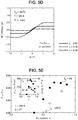
Fig. 5E is a graph showing x dependence of ρyx/ρxx at B = 2T and T = 300K for FexSn1-x films grown at room temperature and FexSn1-x films grown at high temperature. -
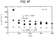
Fig. 5F is a graph showing temperature dependence of Hall conductivity for Fe0.60Sn0.40 films and Fe0.62Sn0.38 films. -
Fig. 6 is graphs showing magnetic field dependence and temperature dependence of Hall resistivity for Fe0.60Sn0.40 films with a film thickness of 40 nm, provided on a polyethylene naphthalate sheet substrate, a glass substrate, and a sapphire substrate, and graphs showing magnetic field dependence and temperature dependence of magnetic sensitivity α = dρyx/dB thereof. -
Fig. 7 is graphs showing temperature dependence of longitudinal resistivity and a variation Δα of magnetic sensitivity for Fe0.60Sn0.40 films with a film thickness of 40 nm provided on various substrates. -
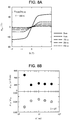
Fig. 8A is a graph showing magnetic field dependence of Hall resistance measured for various film thicknesses. -
Fig. 8B is a graph showing film thickness dependence of longitudinal resistivity, and film thickness dependence of a ratio between Hall resistivity and longitudinal resistivity. -
Fig. 9A is a schematic view illustrating a bending effect experiment of an x-bent device that is a Hall element attached to a surface of a semicircular jig. -
Fig. 9B is a schematic view illustrating a bending effect experiment of a y-bent device that is a Hall element attached to a surface of a semicircular jig. -
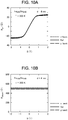
Fig. 10A is a graph showing magnetic field dependence of Hall resistance for Hall elements in a flat state and bent states. -
Fig. 10B is a graph showing magnetic field dependence of sheet resistance for Hall elements in a flat state and bent states. -
Fig. 11 is a table representing properties of Fe-Sn alloys as a non-doped reference sample. -
Fig. 12A is a table representing experimental results of adding Ta to an Fe-Sn alloy in Example 2. -
Fig. 12B is a table representing experimental results of adding W to an Fe-Sn alloy, adding Mo to an Fe-Sn alloy, adding Pt to an Fe-Sn alloy, and adding Mn to an Fe-Sn alloy, in Example 2. -
Fig. 13A is a graph showing magnetic field dependence of Hall resistivity when a thin film is made of Fe0.491Sn0.278Ta0.231. -
Fig. 13B is a graph showing magnetic field dependence of Hall resistivity when a thin film is made of Fe0.446Sn0.326Ta0.228. -
Fig. 13C is a graph showing magnetic field dependence of Hall resistivity when a thin film is made of Fe0.434Sn0.313Ta0.253. -
Fig. 13D is a graph showing magnetic field dependence of Hall resistivity when a thin film is made of Fe0.381Sn0.379Ta0.240. -
Fig. 13E is a graph showing magnetic field dependence of Hall resistivity when a thin film is made of Fe0.589Sn0.345Pt0.066. -
Fig. 13F is a graph showing magnetic field dependence of Hall resistivity when a thin film is made of Fe0.409Sn0.360Mn0.231. -
Fig. 13G is a graph showing magnetic field dependence of Hall resistivity when a thin film is made of Fe0.551Sn0.349W0.100. -
Fig. 13H is a graph showing magnetic field dependence of Hall resistivity when a thin film is made of Fe0.541Sn0.325W0.134. -
Fig. 13I is a graph showing magnetic field dependence of Hall resistivity when a thin film is made of Fe0.575Sn0.347Mo0.078. -
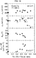
Fig. 14 is graphs of composition dependence of longitudinal resistivity, Hall resistivity, a saturation magnetic field, and a magnetic sensitivity when a thin film is made of Fe, Sn, and Ta. -
Fig. 15 is a table representing experimental results of adding In to an Fe-Sn alloy and adding Ge to an Fe-Sn alloy in Example 3. -
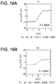
Fig. 16A is a graph showing magnetic field dependence of Hall resistivity when a thin film is made of Fe0.611Sn0.308In0.081. -
Fig. 16B is a graph showing magnetic field dependence of Hall resistivity when a thin film is made of Fe0.583Sn0.300Ge0.117. -
Fig. 17 is a graph showing a relationship between a saturation magnetic field and a magnetic sensitivity for ternary compounds and non-doped reference samples according to Example 2 and Example 3. - Hereinafter, embodiments of the invention will be described with reference to the drawings. The same reference signs are used to designate the same or similar elements throughout the drawings. The drawings are schematic, and a relationship between a planar dimension and a thickness and a thickness ratio between members are different from reality. Needless to say, there are portions having different dimensional relationships or ratios between the drawings.
- First, the configuration of a
Hall element 100 according to the embodiments will be described. - As shown in
Fig. 1 , theHall element 100 includes asubstrate 1, and athin film 2 as a magneto-sensitive layer on thesubstrate 1. Thethin film 2 contains an alloy of Fe and Sn. - Examples of the material of the
substrate 1 include, but are not limited to, polyethylene naphthalate (PEN), polyethylene terephthalate (PET), polyimide, glass, sapphire (single-crystalline Al2O3), alumina (Al2O3 ceramic), magnesium oxide (MgO), strontium titanate (SrTiO3), quartz (SiO2), silicon (Si), gallium arsenide (GaAs), or indium phosphide (InP) . - As shown in
Fig. 1 andFig. 2 , thethin film 2 has a Hall-bar structure with sixterminals 21 to 26. In the embodiments, a thickness of thethin film 2 is denoted by d, a distance between theterminals thin film 2 is denoted by W. Instead of the six-terminal Hall-bar structure shown inFig. 1 andFig. 2 , a four-terminal, cross-shaped Hall-bar structure may be employed. - When a magnetic field B is applied in an out-of-plane direction of the
thin film 2, and an electric current I flows between theterminals Fig. 1 , a longitudinal voltage Vxx = RxxI that is parallel to the electric current I is generated between theterminals terminals - Reference will be made below to Example 1 in which the
thin film 2 is made of an Fe-Sn alloy, and Example 2 and Example 3 in which thethin film 2 is made of a ternary compound of an Fe-Sn alloy and a dopant element (impurities). - A FexSn1-x film is prepared by radio-frequency (RF) magnetron sputtering, for example. As shown in the inset of
Fig. 3 , Fe chips are placed on an Sn target, and an Fe content x in the FexSn1-x film is controlled by changing the number of Fe chips on the Sn target. In the inset ofFig. 3 , a white scale bar represents 10 mm.Fig. 3 shows a relationship between the number of Fe chips and the Fe content x. InFig. 3 , x = 0.50, 0.60, and 0.75 correspond to FeSn, Fe3Sn2, and Fe3Sn, respectively. The sputtering as described above is an industrially general-purpose technique, and makes it possible to prepare a highly-uniform thin film and easily spread the thin film over a large area. Alternative techniques for attaining a similar composition of Fe and Sn may include the use of an alloy target in which the composition of Fe and Sn is tuned, or supplying Fe and Sn from different sputtering sources to tune the composition of the thin film. Any of these techniques may be employed. -
Fig. 4A shows X-ray diffraction (XRD) patterns for Fe0.60Sn0.40 films with a film thickness d = 40 nm, grown on a sapphire substrate, a glass substrate, and a PEN sheet substrate at room temperature (a growth temperature Tg = RT).Fig. 4A indicates that the room-temperature grown samples do not have crystalline character and are expected to have excellent uniformity. -
Fig. 4B shows XRD patterns for FexSn1-x films with x = 0.54, 0.62, and 0.78, grown on sapphire substrates at high temperature (Tg = 500°C). The film thicknesses d are approximately 40 nm.Fig. 4B indicates that a crystalline sample can be also prepared by high-temperature growth. - Next, the Hall effect obtained from the measurement of electrical transport properties for FexSn1-x films will be described with reference to
Fig. 5A to Fig. 5F . The electrical transport properties are measured using VersaLab (Quantum Design), a physical property measurement system (Quantum Design), and a power-supply measurement unit. -
Fig. 5A andFig. 5B show magnetic field dependence of Hall resistivity ρyx and magnetization M measured when applying the magnetic field B in an out-of-plane direction at T = 300K to non-crystalline FexSn1-x films with different x, grown on sapphire substrates at room temperature.Fig. 5C and -
Fig. 5D show magnetic field dependence of the Hall resistivity ρyx and the magnetization M measured when applying the magnetic field B in an out-of-plane direction at T = 300K to crystalline FexSn1-x films with different x, grown on sapphire substrates at high temperature. As it is obvious fromFig. 5A to Fig. 5D , the behavior of the Hall resistivity ρyx is remarkably similar to magnetization curves, indicating that the response of the Hall resistivity ρyx results from the anomalous Hall effect, and an anomalous Hall effect contribution is dominant over an ordinary Hall effect contribution. However,Fig. 5C andFig. 5D suggest that high-temperature growth for x = 0.54 exhibits an extremely small anomalous Hall effect. -
Fig. 5E shows x dependence of ρyx/ρxx at B = 2T and T = 300K for non-crystalline FexSn1-x films grown at room temperature (filled circles) and crystalline FexSn1-x films grown at high temperature (open circles). Here, ρxx is longitudinal resistivity. The inset ofFig. 5E shows the longitudinal resistivity ρxx (triangles) and the Hall resistivity ρyx (squares) for the non-crystalline FexSn1-x films. The inset ofFig. 5E indicates that the Hall resistivity ρyx has a sharp peak in the vicinity of x = 0.60 and the longitudinal resistivity ρxx is slightly changed with respect to x. As a result, as shown inFig. 5E , ρyx/ρxx for the non-crystalline films is 0.02 or more in 0.50 ≤ x < 0.90, in particular, is maximized (approximately 0.05) in the vicinity of x = 0.60 to 0.75. ρyx/ρxx of the crystalline films shows a similar behavior, but is smaller than ρyx/ρxx of the non-crystalline films. -
Fig. 5F shows temperature dependence of Hall conductivity σxy = ρyx/(ρxx 2 + ρyx 2) for non-crystalline Fe0.60Sn0.40 films (filled circles) and crystalline Fe0.62Sn0.38 films (open circles). For reference, inFig. 5F , data plots (squares) of bulk Fe3Sn2 single crystals described in the following literature are also included: Ye, L. et al. "Massive Dirac fermions in a ferromagnetic kagome metal," Nature 555, 638-642 (2018). -
Fig. 5F indicates that the Hall conductivity σxy of the crystalline films rarely depends on the temperature T, and resembles the intrinsic behavior of the Fe3Sn2 single crystals, but is smaller than the Hall conductivity σxy of the bulk Fe3Sn2, suggesting that the crystallization of Fe3Sn2 is accelerated by high-temperature sputtering (Tg = 500°C) to form polycrystals. In stark contrast, the Hall conductivity σxy of the non-crystalline films rivals the Hall conductivity σxy of the bulk Fe3Sn2 over a wide range of temperature. - Next, the sensitivity of the
Hall element 100 will be described. - For the ordinary Hall effect sensing, the Hall voltage Vyx when driving with a constant voltage is defined as Equation (1).

- Here, µ is a mobility, and Vin is an input voltage for allowing an electric current to flow (the longitudinal voltage Vxx shown in
Fig. 1 andFig. 2 ). Hence, the Hall voltage Vyx is determined by the mobility µ except for the magnetic field B and a geometrical factor W/L, and the sensitivity can be obtained from the mobility µ. - For the anomalous Hall effect sensing, on the other hand, the Hall voltage Vyx is defined as Equation (2).

- Here, Iin represents an electric current (the electric current I shown in
Fig. 1 andFig. 2 ), and the Hall resistivity ρyx is a function of the magnetic field B. From Equation (2), the sensitivity of theHall element 100 can be obtained from dρyx/dB and ρyx/ρxx. - In order to compare temperature stability of an ordinary semiconductor Hall element with that of the Hall element utilizing the anomalous Hall effect, the temperature stability of the mobility µ and that of ρyx/ρxx are used as their indexes, respectively. The temperature stability in this ρyx/ρxx term is high, and thus, the temperature stability of the
Hall element 100 of the embodiments is more excellent than that of the ordinary semiconductor Hall element. - A sensitivity coefficient is given by Equation (3).

- Substituting Vyx = RyxI, Ryx = ρyx/d, Vin= RxxI, and Rxx = ρxxL/Wd into Equation (3) yields a sensitivity coefficient = (ρyx/ρxx) × (W/L) × (1/B). If ρyx/ρxx = 0.04 from
Fig. 5E , the geometrical factor W/L = 1, and B = 0.6T within -0.6T ≤ B ≤ 0.6T which is a linear region of the magnetic field B as shown inFig. 5A andFig. 5B , then the sensitivity coefficient = 0.04 × 1 ÷ 0.6 = 0.066 (V/T/V) = 0.066 (mV/mT/V) is obtained. This value of the sensitivity coefficient is approximately 1/3 of a sensitivity coefficient of GaAs 650 Ohm element, which is approximately 0.25 mV/mT/V representing a standard sensitivity, and is expected to increase by tuning the configuration, the composition, or the like (refer to Pham Nam hai, "Super-high-sensitivity anomalous Hall effect magnetic sensor," New Technology Presentation Meetings!). - Next, the anomalous Hall effect on various substrates will be described with reference to
Fig. 6 andFig. 7 . - Graphs a of
Fig. 6 show magnetic field dependence and temperature dependence of the Hall resistivity ρyx for Fe0.60Sn0.40 films with a film thickness d = 40 nm, provided on each of a flexible PEN sheet substrate, a glass substrate, and a sapphire substrate. The Hall resistivity ρyx is measured at T = 50K, 100K, 150K, 200K, 250K, 300K, 350K, and 400K. Data at T = 300K are indicated by a thick line. The graphs a ofFig. 6 clearly demonstrate that the anomalous Hall effects on those three substrates are essentially the same, meaning that no specific substrate is required in order to attain a giant anomalous Hall effect. - Graphs b of
Fig. 6 show the results of calculating the magnetic sensitivity α = dρyx/dB (B≥0T) from data on various substrates shown in the graphs a ofFig. 6 . Each inset in the graphs b ofFig. 6 shows contour plots of the magnetic sensitivity α against the temperature T and the magnetic field B. The graphs b ofFig. 6 indicate that the magnetic sensitivity α is almost constant at a high magnetic field and is rarely affected by a temperature change. This is also obvious from a variation of the magnetic sensitivity α as described below. - A lower graph of
Fig. 7 shows a temperature change (variation) of the magnetic sensitivity α that is defined as Δα = (α(T) - α (T = 300K))/α(T = 300K). This lower graph indicates that the variation Δα is within a few percent (-5% to +5%) on any of the substrates in an operation temperature range of T = 200K to 400K, and is equivalent to that of IC compensated semiconductors. As shown in an upper graph ofFig. 7 , a change in the longitudinal resistivity ρxx with respect to the temperature T is extremely small on any of the substrates . This indicates that theHall element 100 of the embodiments has an advantage over semiconductor devices with thermally activated transport properties. - Next, in order to further increase the Hall voltage (Vyx = I × Ryx = I × ρyx/d) from the viewpoint of the film thickness d, film thickness dependence of the anomalous Hall effect will be described.
Fig. 8A shows magnetic field dependence of the Hall resistance Ryx for Fe0.60Sn0.40 films at T = 300K, measured with the film thickness d = 2 nm, 4 nm, 10 nm, 20 nm, and 40 nm. In addition,Fig. 8B shows film thickness dependence of the longitudinal resistivity ρxx and ρyx/ρxx for the Fe0.60Sn0.40 films.Fig. 8A and Fig. 8B indicate that with the film thickness d of 4 nm or more, ρyx/ρxx can be maintained at 0.04 to 0.05, and a giant anomalous Hall effect occurs. In particular,Fig. 8B indicates that ρyx/ρxx is maintained at approximately a constant value with the film thickness d of 20 nm or more, implying almost no film thickness dependence. On the other hand, when the film thickness decreases to d = 2 nm, the longitudinal resistivity ρxx rapidly increases, and ρyx/ρxx rapidly decreases. The change of the width W and/or the length L other than the film thickness d to fabricate a new Hall element may lead to the enhancement of the anomalous Hall effect. - Next, bending measurement of the
Hall element 100 will be described. - As shown in
Fig. 9A and Fig. 9B , two types of devices (an x-bent device and a y-bent device), each attached to a surface of a semicircular jig with a radius of 4.9 mm, are prepared. Each of the x-bent device and the y-bent device is theHall element 100 in which an Fe0.60Sn0.40 film with d = 4 nm is provided on a flexible PEN sheet substrate. The x-bent device shown inFig. 9A is attached to the semicircular jig such that the direction of the electric current I is parallel to a circumferential direction of the semicircular jig. The y-bent device shown inFig. 9B is attached to the semicircular jig such that the direction of the electric current I is parallel to an axial direction of the semicircular jig. -
Fig. 10A shows magnetic field dependence of the Hall resistance Ryx for a Hall element in a flat state and Hall elements in bent states (that is, the x-bent device and the y-bent device), andFig. 10B shows magnetic field dependence of sheet resistance Rsheet for such Hall elements. As it is obvious fromFig. 10A and Fig. 10B , no remarkable difference is found in the anomalous Hall effect between the flat state and the bent states, and damage including fracture does not occur in a range of a measured curvature radius. - As described above, according to Example 1, providing the
Hall element 100 including thethin film 2 made of a non-toxic and inexpensive alloy of Fe and Sn (FexSn1-x (0.5 ≤ x < 0.9)) enables stability in a wide range of temperature including a room temperature, and detection of the Hall voltage as with the conventional semiconductors. In addition, it is possible to prepare the highly-uniformthin film 2 on thesubstrate 1 by a general-purpose technique such as sputtering. It is also possible to achieve a linear output (a soft magnetic body) in a comparatively wide range of magnetic field (for example, in a range of -0.6T to +0.6T). Further, the material of thesubstrate 1 is not particularly limited, unlike substrates used in the conventional Hall elements, such as a GaAs single-crystalline substrate. In addition, a flexible substrate can also be employed. This makes it possible to achieve a small andlightweight Hall element 100. - Example 2 demonstrates the anomalous Hall effect when the
thin film 2 is a ternary compound containing an Fe-Sn alloy and a dopant element (impurity), and the dopant element is a transition metal element that is added in order to modulate spin-orbit coupling or magnetism. - In Example 2, the
thin film 2 containing a ternary compound is provided on thesapphire substrate 1. -
Fig. 11 shows properties of an Fe-Sn alloy as a non-doped reference sample that is used in the measurement of an impurity doping effect or comparative verification.Fig. 11 shows sample IDs of five Fe-Sn alloys as non-doped reference samples denoted by N1 to N5, respectively, and results of measuring the film thickness d, the Hall resistivity ρyx at the magnetic field B = 2T, ρyx/ρxx at the magnetic field B = 2T, the magnetic sensitivity dρyx/dB at the magnetic field B ≤ 0.2T, a carrier density, and a composition ratio, for each of the non-doped reference samples. The composition ratio represents the results from energy dispersive X-ray spectrometry (EDX). The carrier density of the non-doped reference samples N1 and N3 to N5 is not analyzed. - In Example 2, experiments of adding each of tantalum (Ta), tungsten (W), molybdenum (Mo), platinum (Pt), and manganese (Mn) to a non-doped reference sample N2 are performed by room-temperature sputtering. The addition of Ta, the addition of W, the addition of Mo, and the addition of Pt are mainly aimed at modulating spin-orbit coupling, and the addition of Mn is mainly aimed at modulating magnetism.
- In Example 2, let us suppose that an Fe site of the non-doped reference sample N2 is substituted with a dopant X, and a doping level representing a doping rate is defined as X/(Fe + X).
-
Fig. 12A shows experimental results of adding Ta to the non-doped reference sample N2, andFig. 12B shows experimental results of adding W to the non-doped reference sample N2, adding Mo to the non-doped reference sample N2, adding Pt to the non-doped reference sample N2, and adding Mn to the non-doped reference sample N2.Fig. 12A andFig. 12B show the dopant X, the sample ID, the film thickness d, the Hall resistivity ρyx at the magnetic field B = 2T, ρyx/ρxx at the magnetic field B = 2T, the magnetic sensitivity dρyx/dB at the magnetic field B ≤ 0.2T, the carrier density, the composition ratio obtained from EDX, and the doping level, for each experiment. - In
Fig. 12A , nine sample IDs of the dopant Ta are denoted by T1 to T9 in ascending order of the doping level. InFig. 12B , two sample IDs of the dopant W are denoted by W1 and W2 in ascending order of the doping level, a sample ID of the dopant Mo is denoted by O1, a sample ID of the dopant Pt is denoted by P1, and a sample ID of the dopant Mn is denoted by M1. - In the samples T8 and T9, magnetic field dependence of the Hall resistivity ρyx is non-linear in the measured magnetic field range, and thus, the magnetic sensitivity dρyx/dB and the carrier density are not obtained.
-
Fig. 13A, Fig. 13B, Fig. 13C , andFig. 13D show magnetic field dependence of the Hall resistivity ρyx for the samples T4, T5, T6, and T7 at T = 300K, respectively, andFig. 13E, Fig. 13F ,Fig. 13G, Fig. 13H, and Fig. 13I show magnetic field dependence of the Hall resistivity ρyx for the samples P1, M1, W1, W2, and O1 at T = 300K, respectively. -
Fig. 14 shows the longitudinal resistivity ρxx at the magnetic field B = 2T, the Hall resistivity ρyx at the magnetic field B = 2T, a saturation magnetic field Bsat, and composition dependence (doping level dependence) of the magnetic sensitivity dρyx/dB at T = 300K and the magnetic field B ≤ 0.2T, for the samples T1 to T9 obtained from the experiments of adding Ta to the non-doped reference sample N2, and for the non-doped reference sample N2. - As shown in
Fig. 12A andFig. 14 , the Hall resistivity ρyx of the samples T1 and T3 to T6 is higher than that of the non-doped reference sample N2, and the magnetic sensitivity dρyx/dB of the samples T2 to T7 is higher than that of the non-doped reference sample N2. As shown inFig. 12A , ρyx/ρxx of the samples T1 and T4 is higher than that of the non-doped reference sample N2. As shown inFig. 12B , the magnetic sensitivity dρyx/dB of the samples W1, W2, and O1 is higher than that of the non-doped reference sample N2. -
Fig. 12A andFig. 14 suggest that for the samples T3, T4, T5, and T6 (the doping level = 0.27 to 0.37), both of the Hall resistivity ρyx and the magnetic sensitivity dρyx/dB are enhanced compared to the non-doped reference sample N2, indicating that even larger anomalous Hall effect occurs. - For the samples T5, T6, and T7, as shown in
Fig. 12A ,Fig. 13B to Fig. 13D , andFig. 14 , the magnetic sensitivity dρyx/dB at a low magnetic field (B ≤ 0.2T) is extremely high compared to the non-doped reference sample N2. In particular, for the sample T5, both of the Hall resistivity ρyx and the magnetic sensitivity dρyx/dB are the highest, and the magnetic sensitivity dρyx/dB (29.1 µΩcm/T) even approaches twice that of the non-doped reference sample N2. - In contrast,
Fig. 13B to Fig. 13D andFig. 14 suggest that the saturation magnetic field Bsat (a maximum detectable magnetic field) of the samples T5, T6, and T7 is slightly less than that of the non-doped reference sample N2, but is maintained at approximately 0.2T to 0.4T. - As shown in
Fig. 8B , for the Fe-Sn alloy of Example 1, ρyx/ρxx rarely depends on the film thickness d at the film thickness of 20 nm or more. In Example 2, as shown inFig. 12A andFig. 12B , the film thicknesses d of all of the samples T1 to T9, W1, W2, O1, P1, and M1 are in a range of 35 nm to 65 nm, which is sufficiently greater than 20 nm. Accordingly, a change in various parameters such as the Hall resistivity ρyx, ρyx/ρxx, and the magnetic sensitivity dρyx/dB rarely depends on the film thickness d, and the improvement of the properties of the samples in Example 2 is attributed to impurity doping. - Example 3 demonstrates the anomalous Hall effect when the
thin film 2 is a ternary compound containing an Fe-Sn alloy and a dopant element (impurity), and the dopant element is a main-group element that is added in order to modulate carrier density or density of states. - Also in Example 3, the
thin film 2 containing a ternary compound is provided on thesapphire substrate 1. - In Example 3, experiments of adding each of indium (In) and germanium (Ge) to the non-doped reference sample N2 are performed by room-temperature sputtering. The experimental conditions are the same as those of Example 2. The addition of In having a different number of valence electrons from that of Sn is aimed at modulating carrier density, and the addition of Ge is mainly aimed at modulating density of states.
- In Example 3, let us suppose that an Sn site of the non-doped reference sample N2 is substituted with a dopant X, and a doping level representing a doping rate is defined as X/(Sn + X).
-
Fig. 15 shows experimental results of adding In to the non-doped reference sample N2 and adding Ge to the non-doped reference sample N2.Fig. 15 shows the dopant X, the sample ID, the film thickness d, the Hall resistivity ρyx at the magnetic field B = 2T, ρyx/ρxx at the magnetic field B = 2T, the magnetic sensitivity dρyx/dB at the magnetic field B ≤ 0.2T, the carrier density, the composition ratio obtained from EDX, and the doping level, for each experiment. - In
Fig. 15 , two sample IDs of the dopant In are denoted by I1 and I2 in ascending order of the doping level, and a sample ID of the dopant Ge is denoted by G1. -
Fig. 16A and Fig. 16B show magnetic field dependence of Hall resistivity ρyx for the samples I1 and G1 at T = 300K, respectively. - As shown in
Fig. 15 , the Hall resistivity ρyx of the sample I1 is higher than that of the non-doped reference sample N2, and ρyx/ρxx of the samples I1 and I2 is higher than that of the non-doped reference sample N2. This indicates that a giant anomalous Hall effect occurs in the samples I1 and I2. - As shown in
Fig. 15 , also in Example 3, the film thicknesses d of all of the samples I1, I2, and G1 are sufficiently greater than 20 nm. Accordingly, a change in various parameters such as the Hall resistivity ρyx, ρyx/ρxx, and the magnetic sensitivity dρyx/dB rarely depends on the film thickness d, and the improvement of the properties of the samples in Example 3 is attributed to impurity doping. -
Fig. 17 shows a relationship between the saturation magnetic field Bsat and the magnetic sensitivity dρyx/dB for the ternary compounds and the non-doped reference samples N1 to N5 according to Example 2 and Example 3. - The data of the samples T3 to T7, W1, W2, and O1 clearly demonstrates that adding Ta, W, or Mo to the non-doped reference sample N2 significantly enhances the magnetic sensitivity dρyx/dB in a low magnetic field region, compared to the non-doped reference sample N2.
- The data of the non-doped reference samples N1 to N5 clearly demonstrates that simply tuning the composition of the Fe-Sn alloy does not provide the magnetic sensitivity dρyx/dB equivalent to that of the samples T3 to T7, W1, W2, and O1.
- A heavy transition metal element such as Ta or W has a strong spin-orbit coupling, and the spin-orbit coupling can be increased by adding such a heavy transition metal element to the Fe-Sn alloy.
- The experimental conditions for adding the impurity described in Example 2 and Example 3 are presented for the purposes of illustration and not limitation. For example, the impurity may be added by a method other than sputtering. In addition, a plurality of impurities may be added. Moreover, the thin film may be provided on a substrate made of a material other than sapphire. In addition, in Example 3, if Sb is added as a main-group element having a different number of valence electrons from that of Sn to modulate carrier density, the anomalous Hall effect may occur.
-
- 100:
- Hall element
- 1:
- Substrate
- 2:
- Thin film
- 21, 22, 23, 24, 25, 26:
- Terminal
Claims (9)
- A Hall element that exhibits an anomalous Hall effect, comprising:a substrate; anda thin film as a magneto-sensitive layer on the substrate, the thin film having a composition of FexSn1-x, where 0.5 ≤ x < 0.9.
- The Hall element according to claim 1, wherein the substrate is made of one of polyethylene naphthalate, polyethylene terephthalate, polyimide, glass, sapphire, alumina, magnesium oxide, strontium titanate, quartz, silicon, gallium arsenide, and indium phosphide.
- The Hall element according to claim 1 or 2, wherein a variation of magnetic sensitivity on the substrate is in a range of -5% to +5% in a temperature range of 200K to 400K.
- The Hall element according to any one of claims 1 to 3, wherein the thin film has a thickness of 4 nm to 40 nm.
- The Hall element according to any one of claims 1 to 4, wherein the substrate is a flexible substrate.
- A Hall element that exhibits an anomalous Hall effect, comprising:a substrate; anda thin film as a magneto-sensitive layer on the substrate, whereinthe thin film is made of an alloy of Fe and Sn, and a dopant element, andthe dopant element is a transition metal element that modulates spin-orbit coupling or magnetism.
- The Hall element according to claim 6, wherein the thin film has a thickness of 35 nm to 65 nm.
- A Hall element that exhibits an anomalous Hall effect, comprising:a substrate; anda thin film as a magneto-sensitive layer on the substrate, whereinthe thin film is made of an alloy of Fe and Sn, and a dopant element, andthe dopant element is a main-group element that has a different number of valence electrons from Sn and modulates carrier density.
- A Hall element that exhibits an anomalous Hall effect, comprising:a substrate; anda thin film as a magneto-sensitive layer on the substrate, whereinthe thin film is made of an alloy of Fe and Sn, and a dopant element, andthe dopant element is a main-group element that modulates density of states.
Applications Claiming Priority (2)
| Application Number | Priority Date | Filing Date | Title |
|---|---|---|---|
| JP2018157542 | 2018-08-24 | ||
| PCT/JP2019/032898 WO2020040264A1 (en) | 2018-08-24 | 2019-08-22 | Hall element |
Publications (2)
| Publication Number | Publication Date |
|---|---|
| EP3843163A1 true EP3843163A1 (en) | 2021-06-30 |
| EP3843163A4 EP3843163A4 (en) | 2023-09-20 |
Family
ID=69593178
Family Applications (1)
| Application Number | Title | Priority Date | Filing Date |
|---|---|---|---|
| EP19853017.2A Pending EP3843163A4 (en) | 2018-08-24 | 2019-08-22 | Hall element |
Country Status (4)
| Country | Link |
|---|---|
| US (1) | US11543468B2 (en) |
| EP (1) | EP3843163A4 (en) |
| JP (1) | JP7461651B2 (en) |
| WO (1) | WO2020040264A1 (en) |
Cited By (1)
| Publication number | Priority date | Publication date | Assignee | Title |
|---|---|---|---|---|
| CN113571632A (en) * | 2021-09-23 | 2021-10-29 | 南开大学 | Abnormal Hall element and preparation method thereof |
Families Citing this family (6)
| Publication number | Priority date | Publication date | Assignee | Title |
|---|---|---|---|---|
| JP7511240B2 (en) * | 2020-12-22 | 2024-07-05 | ユニークチップス合同会社 | Method for forming electrical contacts on semiconductors and conductive thin films, and sheet resistance measurement device, Hall effect measurement device, and capacitance-voltage characteristic measurement device using the same |
| US20250383413A1 (en) * | 2022-02-18 | 2025-12-18 | Tohoku University | Magnetic sensor and magnetic detection method |
| JP7880063B2 (en) * | 2022-05-19 | 2026-06-25 | 株式会社デンソー | Current detection device |
| WO2024079811A1 (en) * | 2022-10-12 | 2024-04-18 | 国立大学法人東北大学 | Thermoelectric conversion device |
| JP7883533B2 (en) * | 2024-03-28 | 2026-07-01 | アルプスアルパイン株式会社 | Magnetic sensor and magnetic measurement method |
| US20250374832A1 (en) * | 2024-05-30 | 2025-12-04 | Uif (University Industry Foundation), Yonsei University | Semiconductor device capable of simultaneously changing polarity and magnitude of anomalous hall effect signal according to input current, operating method thereof, and system |
Family Cites Families (13)
| Publication number | Priority date | Publication date | Assignee | Title |
|---|---|---|---|---|
| JPH03129707A (en) * | 1989-07-24 | 1991-06-03 | Matsushita Electric Ind Co Ltd | Soft magnetic thin film and magnetic head using the same |
| JP3180378B2 (en) | 1991-09-11 | 2001-06-25 | 松下電器産業株式会社 | Method of manufacturing semiconductor thin film and method of manufacturing semiconductor magnetoresistive element |
| JP2001102656A (en) | 1999-09-30 | 2001-04-13 | Res Inst Electric Magnetic Alloys | Ferromagnetic Hall element |
| JP2002016330A (en) | 2000-06-30 | 2002-01-18 | Sanyo:Kk | Component mounting board and method of manufacturing the same |
| JP3730518B2 (en) * | 2001-01-19 | 2006-01-05 | 株式会社東芝 | Magnetic recording medium |
| JP3955195B2 (en) * | 2001-08-24 | 2007-08-08 | 株式会社日立グローバルストレージテクノロジーズ | Magnetic field sensor and magnetic head |
| JP2004165362A (en) | 2002-11-12 | 2004-06-10 | Rikogaku Shinkokai | Magnetic sensor using Hall effect and method of manufacturing the same |
| US20070154629A1 (en) * | 2003-08-29 | 2007-07-05 | Japan Science And Technology Agency | Thin ito films and method of producing the same |
| US20070046285A1 (en) * | 2005-08-29 | 2007-03-01 | Kenta Arima | Sample observation method and observation device |
| JP4904352B2 (en) * | 2006-07-26 | 2012-03-28 | アルプス電気株式会社 | Magnetic sensor |
| US8722441B2 (en) * | 2010-01-21 | 2014-05-13 | Siphoton Inc. | Manufacturing process for solid state lighting device on a conductive substrate |
| JP6064344B2 (en) | 2012-03-16 | 2017-01-25 | 富士通株式会社 | Magnetic detector |
| US9780299B2 (en) * | 2015-11-23 | 2017-10-03 | Headway Technologies, Inc. | Multilayer structure for reducing film roughness in magnetic devices |
-
2019
- 2019-08-22 WO PCT/JP2019/032898 patent/WO2020040264A1/en not_active Ceased
- 2019-08-22 EP EP19853017.2A patent/EP3843163A4/en active Pending
- 2019-08-22 US US17/269,566 patent/US11543468B2/en active Active
- 2019-08-22 JP JP2020538470A patent/JP7461651B2/en active Active
Cited By (2)
| Publication number | Priority date | Publication date | Assignee | Title |
|---|---|---|---|---|
| CN113571632A (en) * | 2021-09-23 | 2021-10-29 | 南开大学 | Abnormal Hall element and preparation method thereof |
| CN113571632B (en) * | 2021-09-23 | 2021-12-10 | 南开大学 | A kind of abnormal Hall element and preparation method thereof |
Also Published As
| Publication number | Publication date |
|---|---|
| US20210293905A1 (en) | 2021-09-23 |
| EP3843163A4 (en) | 2023-09-20 |
| JP7461651B2 (en) | 2024-04-04 |
| US11543468B2 (en) | 2023-01-03 |
| WO2020040264A1 (en) | 2020-02-27 |
| JPWO2020040264A1 (en) | 2021-09-16 |
Similar Documents
| Publication | Publication Date | Title |
|---|---|---|
| US11543468B2 (en) | Hall element | |
| Fijalkowski et al. | Coexistence of surface and bulk ferromagnetism mimics skyrmion Hall effect in a topological insulator | |
| Suzuki et al. | Large anomalous Hall effect in a half-Heusler antiferromagnet | |
| Chiu et al. | Weak antilocalization in topological insulator Bi 2 Te 3 microflakes | |
| Chambers et al. | New possibilities for ferromagnetic semiconductors | |
| US10832711B2 (en) | Beta tungsten thin films with giant spin Hall effect for use in compositions and structures with perpendicular magnetic anisotropy | |
| Liang et al. | Inducing ferromagnetism and Kondo effect in platinum by paramagnetic ionic gating | |
| EP3176843B1 (en) | Magnetoresistive element, magnetic head using magnetoresistive element, and magnetic playback device | |
| CN113728447A (en) | Thermoelectric conversion element and thermoelectric conversion device | |
| Jena et al. | Scaling analysis of anomalous Hall resistivity in the Co2TiAl Heusler alloy | |
| Yamasaki et al. | Observation of anomalous Hall effect in EuO epitaxial thin films grown by a pulse laser deposition | |
| Lukose et al. | Hybrid graphene-manganite thin film structure for magnetoresistive sensor application | |
| Lao et al. | Strong perpendicular uniaxial magnetic anisotropy in tetragonal Fe 0.5 Co 0.5 films of artificially ordered B2 state | |
| Harrington et al. | Growth, electrical, structural, and magnetic properties of half-Heusler CoT i 1− x F ex Sb | |
| Zhu et al. | Giant coercivity, resistivity upturn, and anomalous Hall effect in ferrimagnetic FeTb | |
| Saypulaeva et al. | Effect of hydrostatic pressures of up to 9 GPa on the galvanomagnetic properties of Cd3As2–MnAs (20 mol% MnAs) alloy in a transverse magnetic field | |
| Yuan et al. | Topological Hall effect and the transition of the anomalous Hall effect mechanism in hexagonal alloys Mn3. 1− xFexGe0. 9 (x= 1.6, 1.8, 2.0) | |
| Shiozaki et al. | Galvanomagnetic measurements in Fe3O4 | |
| JP6967259B2 (en) | High-sensitivity surface direct energization giant magnetoresistive element and its applications | |
| Golias et al. | Magnetization relaxation and search for the magnetic gap in bulk-insulating V-doped (Bi, Sb) 2Te3 | |
| Lamichhane et al. | Study of the ferromagnetic quantum phase transition in Ce3− x Mg x Co9 | |
| Cheng et al. | Atomic layer molecular beam epitaxy of kagome magnet RMn6Sn6 (R= Er, Tb) thin films | |
| US12442871B2 (en) | Magnetoresistive element having compensated temperature coefficient of TMR | |
| Liao et al. | Tuning properties of columnar nanocomposite oxides | |
| Hnida et al. | Room-temperature ferromagnetism in InSb-Mn nanowires |
Legal Events
| Date | Code | Title | Description |
|---|---|---|---|
| STAA | Information on the status of an ep patent application or granted ep patent |
Free format text: STATUS: THE INTERNATIONAL PUBLICATION HAS BEEN MADE |
|
| PUAI | Public reference made under article 153(3) epc to a published international application that has entered the european phase |
Free format text: ORIGINAL CODE: 0009012 |
|
| STAA | Information on the status of an ep patent application or granted ep patent |
Free format text: STATUS: REQUEST FOR EXAMINATION WAS MADE |
|
| 17P | Request for examination filed |
Effective date: 20210324 |
|
| AK | Designated contracting states |
Kind code of ref document: A1 Designated state(s): AL AT BE BG CH CY CZ DE DK EE ES FI FR GB GR HR HU IE IS IT LI LT LU LV MC MK MT NL NO PL PT RO RS SE SI SK SM TR |
|
| DAV | Request for validation of the european patent (deleted) | ||
| DAX | Request for extension of the european patent (deleted) | ||
| REG | Reference to a national code |
Ref country code: DE Ref legal event code: R079 Free format text: PREVIOUS MAIN CLASS: H01L0043060000 Ipc: H10N0052850000 |
|
| A4 | Supplementary search report drawn up and despatched |
Effective date: 20230823 |
|
| RIC1 | Information provided on ipc code assigned before grant |
Ipc: H01F 10/14 20060101ALI20230817BHEP Ipc: H10N 52/00 20230101ALI20230817BHEP Ipc: H10N 52/85 20230101AFI20230817BHEP |
|
| STAA | Information on the status of an ep patent application or granted ep patent |
Free format text: STATUS: EXAMINATION IS IN PROGRESS |
|
| 17Q | First examination report despatched |
Effective date: 20250403 |
|
| RIC1 | Information provided on ipc code assigned before grant |
Ipc: H10N 52/85 20230101AFI20260410BHEP Ipc: H10N 52/00 20230101ALI20260410BHEP Ipc: H01F 10/13 20060101ALI20260410BHEP Ipc: H01F 10/14 20060101ALN20260410BHEP |
|
| GRAP | Despatch of communication of intention to grant a patent |
Free format text: ORIGINAL CODE: EPIDOSNIGR1 |
|
| STAA | Information on the status of an ep patent application or granted ep patent |
Free format text: STATUS: GRANT OF PATENT IS INTENDED |
|
| INTG | Intention to grant announced |
Effective date: 20260521 |