EP3842982A1 - Hierarchical random scrambling of secure data storage resulting in randomness across chips and on power on resets of individual chips - Google Patents
Hierarchical random scrambling of secure data storage resulting in randomness across chips and on power on resets of individual chips Download PDFInfo
- Publication number
- EP3842982A1 EP3842982A1 EP20214500.9A EP20214500A EP3842982A1 EP 3842982 A1 EP3842982 A1 EP 3842982A1 EP 20214500 A EP20214500 A EP 20214500A EP 3842982 A1 EP3842982 A1 EP 3842982A1
- Authority
- EP
- European Patent Office
- Prior art keywords
- rnd
- data
- physical address
- bit
- logical address
- Prior art date
- Legal status (The legal status is an assumption and is not a legal conclusion. Google has not performed a legal analysis and makes no representation as to the accuracy of the status listed.)
- Granted
Links
Images




Classifications
-
- G—PHYSICS
- G06—COMPUTING OR CALCULATING; COUNTING
- G06F—ELECTRIC DIGITAL DATA PROCESSING
- G06F21/00—Security arrangements for protecting computers, components thereof, programs or data against unauthorised activity
- G06F21/60—Protecting data
- G06F21/62—Protecting access to data via a platform, e.g. using keys or access control rules
- G06F21/6218—Protecting access to data via a platform, e.g. using keys or access control rules to a system of files or objects, e.g. local or distributed file system or database
- G06F21/6227—Protecting access to data via a platform, e.g. using keys or access control rules to a system of files or objects, e.g. local or distributed file system or database where protection concerns the structure of data, e.g. records, types, queries
-
- G—PHYSICS
- G06—COMPUTING OR CALCULATING; COUNTING
- G06F—ELECTRIC DIGITAL DATA PROCESSING
- G06F12/00—Accessing, addressing or allocating within memory systems or architectures
- G06F12/14—Protection against unauthorised use of memory or access to memory
- G06F12/1416—Protection against unauthorised use of memory or access to memory by checking the object accessibility, e.g. type of access defined by the memory independently of subject rights
- G06F12/1425—Protection against unauthorised use of memory or access to memory by checking the object accessibility, e.g. type of access defined by the memory independently of subject rights the protection being physical, e.g. cell, word, block
-
- G—PHYSICS
- G06—COMPUTING OR CALCULATING; COUNTING
- G06F—ELECTRIC DIGITAL DATA PROCESSING
- G06F21/00—Security arrangements for protecting computers, components thereof, programs or data against unauthorised activity
- G06F21/70—Protecting specific internal or peripheral components, in which the protection of a component leads to protection of the entire computer
- G06F21/71—Protecting specific internal or peripheral components, in which the protection of a component leads to protection of the entire computer to assure secure computing or processing of information
- G06F21/75—Protecting specific internal or peripheral components, in which the protection of a component leads to protection of the entire computer to assure secure computing or processing of information by inhibiting the analysis of circuitry or operation
- G06F21/755—Protecting specific internal or peripheral components, in which the protection of a component leads to protection of the entire computer to assure secure computing or processing of information by inhibiting the analysis of circuitry or operation with measures against power attack
-
- G—PHYSICS
- G06—COMPUTING OR CALCULATING; COUNTING
- G06F—ELECTRIC DIGITAL DATA PROCESSING
- G06F21/00—Security arrangements for protecting computers, components thereof, programs or data against unauthorised activity
- G06F21/70—Protecting specific internal or peripheral components, in which the protection of a component leads to protection of the entire computer
- G06F21/78—Protecting specific internal or peripheral components, in which the protection of a component leads to protection of the entire computer to assure secure storage of data
- G06F21/79—Protecting specific internal or peripheral components, in which the protection of a component leads to protection of the entire computer to assure secure storage of data in semiconductor storage media, e.g. directly-addressable memories
-
- G—PHYSICS
- G06—COMPUTING OR CALCULATING; COUNTING
- G06F—ELECTRIC DIGITAL DATA PROCESSING
- G06F7/00—Methods or arrangements for processing data by operating upon the order or content of the data handled
- G06F7/58—Random or pseudo-random number generators
- G06F7/588—Random number generators, i.e. based on natural stochastic processes
Definitions
- This application is directed to the field of secure data storage involving the hierarchical scrambling of secure data across chips and at every power on reset of individual chips based upon parts of a random number.
- a secure data storage device includes a random number generator configured to generate a random number in response to an event, a volatile storage, and a code randomizer.
- the code randomizer is configured to generate hierarchical part alignment selectors from the random number. For each of a plurality of secure data blocks to be stored in the volatile storage, the code randomizer is configured to set a physical address of a first logical address for that secure data block within the volatile storage based upon the hierarchical part alignment selectors. For each of a plurality of data words within that secure data block, the code randomizer is configured to set a physical address of a first logical address for that data word based upon the hierarchical part alignment selectors.
- the code randomizer For each of a plurality of data bytes within that data word, the code randomizer is configured to set a physical address of a first logical address for that data byte based upon the hierarchical part alignment selectors, and set a physical address of a logical address for a first of a plurality of data bits within that data byte based upon the hierarchical part alignment selectors.
- Each data bit, data byte, data word, and secure data block is stored in the volatile storage according to the set physical addresses therefor.
- the code randomizer may be configured to, for each of the plurality of secure data blocks, set a physical address of each subsequent logical address for that secure data block by incrementing the physical address of an immediately preceding logical address for that secure data block. For each of the plurality of data words within that secure data block, the code randomizer may be configured to set a physical address of each subsequent logical address for that data word by incrementing the physical address of an immediately preceding logical address for that data word.
- the code randomizer may be configured to set a physical address of each subsequent logical address for that data byte by incrementing the physical address of an immediately preceding logical address for that data byte, and set a physical address of each subsequent data bit of that data word by incrementing the physical address of an immediately preceding data bit of that data word.
- the secure data storage device 20 includes a non-volatile password store 22, a volatile password store 23, comparison logic 24, a secure resource 25, and control logic 21 (such as a code randomizer, which will be explained below).
- the non-volatile password store 22 copies its stored secure content to a volatile password store 23 over an interface (described below, and shown in FIG. 1B as 26).
- the stored secure content is, as will be explained below in detail, copied from the non-volatile password store 22 to the volatile password store 23 and stored in the volatile password store 23 pursuant to hierarchical part alignment selectors generated by the control logic 21.
- the user is challenged to provide a challenge response that matches a password stored in the volatile password store 23.
- the challenge response is received at the comparison logic 24, which unlocks the secure resource 25 to permit reading from and/or writing to the secure resource 25 by the user if the challenge response matches the password stored in the volatile password store 23. If the challenge response does not match the password stored in the volatile password store 23, the comparison logic 24 does not grant access to the secure resource 25.
- the code randomizer 21 upon startup, upon a power-on reset, and/or upon occurrence of a given event (such as any operation performed on the volatile password store 23) sends a random number generation request (Rand.Gen) to a random number generator 27, which responds by sending a random number to the code randomizer 21.
- the code randomizer 21 may also send the random number generation request to the random number generator 27 periodically during operation, or asynchronously during operation (such as randomly during operation).
- the random number generator 27 may be any type of random number generator, such as a true random number generator or psuedo-random number generator.
- the code randomizer 21 From the random number, the code randomizer 21 generates hierarchical part alignment selectors (also referred to as storage and transport codes) which, as will be explained below in detail, will be used to control storage of the secure data in the volatile password store 23 through the interface 26.
- the code randomizer 21 also controls storage of the generated part alignment selectors in the volatile storage 23 so that the part alignment selectors may be used to access the secure data after storage, until the generation of new part alignment selectors.
- new part alignment selectors When new part alignment selectors are generated, the same secure data may be moved and stored pursuant to the part alignment selectors, or new secure data may be stored pursuant to the part alignment selectors.
- the data as stored in the volatile storage 23 is arranged into multiple blocks of secure data. This can be seen in FIG. 2 as Block0, ..., BlockB, with “B” being any integer to denote there may be any such number of blocks of secure data.
- each block is arranged into multiple words, here shown as WordO, ..., WordW, with “W” being any integer to denote that there may be any such number of words per block of secure data. Common word lengths are 16, 32, 64, 128, and 256 bits, for example.
- each word is arranged into multiple bytes, here shown as ByteO, ..., ByteM, with "M” being any integer to denote that there may be any such number of bytes per word.
- each byte is arranged into multiple bits, here shown as BitO, ..., Bit7, with the final bit being Bit7 because a byte contains 8 bits.
- Each bit stored within the volatile storage has a physical address and a logical address.
- Physical address refers to an address directly fed to periphery circuitry that controls access to and from the volatile storage, and is fixed on a bit by bit basis. That is, a given physical address is directly linked to certain physical cells of the volatile storage.
- Logical address refers to an address used by software to access portions of the volatile storage, but that is not directly linked to certain physical cells of the volatile storage. For example, a given logical address may be configured to correspond to a given physical address, or may be reconfigured to correspond to a different physical address on the fly.
- Each block of secure data is stored within a set of physical addresses in the volatile storage 23 that is allocated to that block of secure data.
- Each block of secure data includes multiple data words, with each of those data words being stored within a subset of physical addresses within the set of physical addresses allocated to its associated block of secure data.
- Each data word includes multiple bytes, with each of those bytes being stored within a subset of physical addresses within the subset of physical addresses allocated to that data word.
- Each byte includes multiple bits, with each of those bits being stored within a physical address within the subset of physical addresses allocated to that data byte.
- each block of secure data, each data word, and each byte has a range of logical addresses allocated to it.
- the physical addresses corresponding to the logical addresses are set based upon the hierarchical part alignment selectors.
- the code randomizer 21 generates from the random number a block alignment selector BLK_RND[b:0], a word alignment selector WRD_RND[w:0], a byte alignment selector BYT_RND[m:0], and a bit alignment selector BIT_RND[7:0].
- a block alignment selector BLK_RND[b:0] a word alignment selector WRD_RND[w:0]
- BIT_RND[7:0 bit alignment selector
- block alignment selector BLK_RND[b:0] The effect of the block alignment selector BLK_RND[b:0] can be seen in FIG. 3 . Assume that the blocks of secure data are stored across a given range of contiguous physical addresses, and that the blocks of secure data are stored contiguously with one another.
- Addr0 denotes the first physical address of the first secure data block
- Addr0+BLK_RND denotes the physical address corresponding to the first logical address of the first secure data block (the first logical address of the first secure data block here being denoted as Block0), with physical addresses of subsequent logical addresses of the data blocks being incremented from the physical address of Block0 and wrapping around at the end of storage.
- the block alignment selector BLK_RND[b:0] is equal to 0, meaning that the physical address of Block0 is 0 (equal to the first physical secure data block address).
- the block alignment selector BLK_RND[b:0] is equal to 2, meaning that the physical address of Block0 is 2 (the third physical secure data block address).
- the block alignment selector BLK_RND[b:0] is equal to 3, meaning that the physical address of Block0 is 3 (the fourth physical secure data block address).
- WRD_RND[w:0] denotes the first physical address of the first words in the blocks of secure data (which here are denoted as having a logical address of WordO), with physical addresses of subsequent logical addresses of words being incremented from the physical address of WordO and wrapping around at the end of storage.
- the word alignment selector WRD_RND[w:0] is equal to 0, meaning that the physical address of the WordO in each block of secure data is equal to the first physical word address in each block of secure data.
- the word alignment selector WRD_RND[w:0] is equal to 3, meaning that the physical address of WordO is 3 and therefore equal to the fourth physical word address in each block of secure data.
- the word alignment selector WRD_RND[w:0] is equal to 1, meaning that the physical address of WordO is 1 and therefore equal to the second physical word address in each block of secure data.
- BYT_RND[m:0] denotes the first physical address of the first bytes in the words of the blocks of secure data (which here are denoted as having a logical address of ByteO), with physical addresses of subsequent logical addresses of the bytes being incremented from the physical address of ByteO and wrapping around at the end of storage.
- the byte alignment selector BYT_RND[m:0] is equal to 0, meaning that the physical address of the ByteO in each word of each block of secure data is equal to the first physical byte address in each word in each block of secure data.
- the byte alignment selector BYT_RND[m:0] is equal to 1, meaning that the physical address of ByteO is 1 and therefore equal to the second physical byte address in each word in each block of secure data.
- bit alignment selector BIT_RND[7:0] The effect of the bit alignment selector BIT_RND[7:0] can be seen in FIG. 6 . Assume that the data bits are stored across a given range of contiguous physical addresses, and that the data bits within a given byte are stored contiguously with one another.
- BIT_RND[7:0] denotes the first physical address of the first bits in the bytes of the words of the blocks of secure data (which here are denoted as having a logical address of BitO), with the physical addresses of subsequent logical addresses of the bits being incremented from the physical address of BitO and wrapping around at the end of storage.
- the bit alignment selector BIT_RND[7:0] is equal to 0, meaning that the physical address of the BitO in each byte of each word of each block of secure data is equal to the first physical bit address in each byte of each word in each block of secure data.
- the bit alignment selector BIT_RND[7:0] is equal to 1, meaning that the physical address of BitO is 1 and therefore equal to the second physical bit address in each byte of each word in each block of secure data.
- the code randomizer 21 also controls storage of the generated part alignment selectors BLK_RND[b:0], WRD_RND[w:0], BYT_RND[m:0], and BIT_RND[7:0] into the volatile storage 23 so that the part alignment selectors may be used to access the secure data blocks after storage into the volatile storage 23 pursuant to the generated part alignment selectors.
- the part alignment selectors BLK_RND[b:0], WRD_RND[w:0], BYT_RND[m:0], and BIT_RND[7:0] may be stored in unscrambled form.
- the part alignment selectors BLK_RND[b:0], WRD_RND[w:0], BYT_RND[m:0], and BIT_RND[7:0] may be scrambled upon storage, with the part alignment selector scrambler LVL1_RND[L:0] (also generated from the random number by the code randomizer 21 and stored in the volatile storage 23) being used to denote the first physical address location for each of the part alignment selectors BLK_RND[b:0], WRD_RND[w:0], BYT_RND[m:0], and BIT_RND[7:0].
- LVL1_RND[L:0] is 0, meaning that the first physical address location for each of the part alignment selectors is the first physical address allocated for each of the part alignment selectors.
- LVL1_RND[L:0] changes upon each power-on reset cycle
- LVL1_RND[L:0] is 1, meaning that the first physical address location for each of the part alignment selectors is the second physical address allocated for each of the part alignment selectors, and that the bits of the part alignment selectors wrap around when the end of the allocated physical addresses is reached.
- part alignment selectors BLK_RND[b:0], WRD_RND[w:0], BYT_RND[m:0], and BIT_RND[7:0] may be stored in a logically unscrambled form in chains of flip flops in the volatile storage 23, with ones of those flip flops being scrambled physically in terms of location.
- LVL1_RND[L:0] being used to scramble each part alignment selector
- a different part alignment selector scrambler may be used for each part alignment selector BLK_RND[b:0], WRD_RND[w:0], BYT_RND[m:0], and BIT_RND[7:0].
- the volatile storage 23 may be comprised of volatile memory, and/or flip flops, and that any above described secure data blocks, part scramblers, and part alignment selector scramblers may be saved in the volatile memory and/or the flip flops.
- each bit of each secure data block has been described as being stored contiguously in terms of physical address, and the secure data blocks have been described as being stored contiguously in terms of physical address. Therefore, the incrementation of addresses discussed above has been by one.
- secure data blocks, data words, data bytes, and data bits need not be stored contiguously with each other in terms of physical addresses, and therefore incrementation may simply mean increment by an appropriate number, or to another range of physical addresses so that sometimes incrementation may be by one and sometimes may be by multiple physical addresses.
- the security of the secure data storage device 20 is enhanced by defending against the types of attacks described above in the background. Indeed, it is the use of the part alignment selectors (generated from the random number) to link the physical addresses to the logical addresses that provides this enhance security.
Landscapes
- Engineering & Computer Science (AREA)
- Theoretical Computer Science (AREA)
- Physics & Mathematics (AREA)
- Computer Security & Cryptography (AREA)
- Computer Hardware Design (AREA)
- General Physics & Mathematics (AREA)
- General Engineering & Computer Science (AREA)
- Software Systems (AREA)
- General Health & Medical Sciences (AREA)
- Databases & Information Systems (AREA)
- Health & Medical Sciences (AREA)
- Bioethics (AREA)
- Mathematical Physics (AREA)
- Computational Mathematics (AREA)
- Mathematical Analysis (AREA)
- Mathematical Optimization (AREA)
- Pure & Applied Mathematics (AREA)
- Storage Device Security (AREA)
- Techniques For Improving Reliability Of Storages (AREA)
Abstract

Description
- This application is directed to the field of secure data storage involving the hierarchical scrambling of secure data across chips and at every power on reset of individual chips based upon parts of a random number.
- Data security is of importance in a variety of applications, such as embedded applications. Conventionally, secure data is stored in a sequential manner in a chain of flip flops, and the physical location of these flip flops within a chip is scrambled to as so provide protection against physical hacks.
- This technique, however, is not without drawbacks. First, as should be evident, the scrambling of the physical location of the chained flip flops requires a large amount of interconnection circuitry to provide the connections between the flip flops, consuming area for this routing. In addition, the scrambling remains static across chips of the same design, and remains static within each chip regardless of whether a power on reset of the chip is performed. This fixed routing, and this uniform scrambling between different chips, may not fully prevent sophisticated hacks from recovering at least some of the secure data, which is clearly undesirable.
- As such, further developments into this area are needed.
- A secure data storage device is disclosed herein and includes a random number generator configured to generate a random number in response to an event, a volatile storage, and a code randomizer. The code randomizer is configured to generate hierarchical part alignment selectors from the random number. For each of a plurality of secure data blocks to be stored in the volatile storage, the code randomizer is configured to set a physical address of a first logical address for that secure data block within the volatile storage based upon the hierarchical part alignment selectors. For each of a plurality of data words within that secure data block, the code randomizer is configured to set a physical address of a first logical address for that data word based upon the hierarchical part alignment selectors. For each of a plurality of data bytes within that data word, the code randomizer is configured to set a physical address of a first logical address for that data byte based upon the hierarchical part alignment selectors, and set a physical address of a logical address for a first of a plurality of data bits within that data byte based upon the hierarchical part alignment selectors. Each data bit, data byte, data word, and secure data block is stored in the volatile storage according to the set physical addresses therefor.
- The code randomizer may be configured to, for each of the plurality of secure data blocks, set a physical address of each subsequent logical address for that secure data block by incrementing the physical address of an immediately preceding logical address for that secure data block. For each of the plurality of data words within that secure data block, the code randomizer may be configured to set a physical address of each subsequent logical address for that data word by incrementing the physical address of an immediately preceding logical address for that data word. For each of the plurality of data bytes within that data word, the code randomizer may be configured to set a physical address of each subsequent logical address for that data byte by incrementing the physical address of an immediately preceding logical address for that data byte, and set a physical address of each subsequent data bit of that data word by incrementing the physical address of an immediately preceding data bit of that data word.
-
-
FIG. 1A is a block diagram of a secure data storage device in accordance with this disclosure. -
FIG. 1B is a block diagram showing the secure data storage device ofFIG. 1A when storing secure data in the volatile storage ofFIG. 1A . -
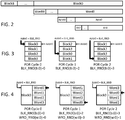
FIG. 2 is a diagram illustrating the division of blocks into words, words into bytes, and bytes into bits. -
FIG. 3 is a diagram illustrating the randomization of the first physical address of Block0 when storing secure data, in the volatile storage ofFIGS. 1A-1B . -
FIG. 4 is a diagram illustrating the randomization of the first physical address of WordO in a given block when storing secure data, in the volatile storage ofFIGS. 1A-1B . -
FIG. 5 is a diagram illustrating the randomization of the first physical address of a byte of a given word in a given block when storing secure data, in the volatile storage system ofFIGS. 1A-1B . -
FIG. 6 is a diagram illustrating the randomization of the first physical address of a given byte of a given word in a given block when storing secure data, in the volatile storage system ofFIGS. 1A-1B . -
FIG. 7 is a diagram illustrating the storage of the random number from which the above randomizations are based upon, and the randomization of the storage of that random number, in the volatile storage ofFIGS. 1A-1B . - The following disclosure enables a person skilled in the art to make and use the subject matter disclosed herein. The general principles described herein may be applied to embodiments and applications other than those detailed above without departing from the spirit and scope of this disclosure. This disclosure is not intended to be limited to the embodiments shown, but is to be accorded the widest scope consistent with the principles and features disclosed or suggested herein.
- With initial reference to
FIG. 1A , a securedata storage device 20 is now described. The securedata storage device 20 includes anon-volatile password store 22, avolatile password store 23,comparison logic 24, asecure resource 25, and control logic 21 (such as a code randomizer, which will be explained below). - In operation, upon powerup or a power-on reset, the
non-volatile password store 22 copies its stored secure content to avolatile password store 23 over an interface (described below, and shown inFIG. 1B as 26). The stored secure content is, as will be explained below in detail, copied from thenon-volatile password store 22 to thevolatile password store 23 and stored in thevolatile password store 23 pursuant to hierarchical part alignment selectors generated by thecontrol logic 21. When a user wants to access thesecure resource 25, the user is challenged to provide a challenge response that matches a password stored in thevolatile password store 23. The challenge response is received at thecomparison logic 24, which unlocks thesecure resource 25 to permit reading from and/or writing to thesecure resource 25 by the user if the challenge response matches the password stored in thevolatile password store 23. If the challenge response does not match the password stored in thevolatile password store 23, thecomparison logic 24 does not grant access to thesecure resource 25. - The storage of the secure content in the
volatile password store 23 will now be described, referring first toFIG. 1B . Thecode randomizer 21, upon startup, upon a power-on reset, and/or upon occurrence of a given event (such as any operation performed on the volatile password store 23) sends a random number generation request (Rand.Gen) to arandom number generator 27, which responds by sending a random number to thecode randomizer 21. Thecode randomizer 21 may also send the random number generation request to therandom number generator 27 periodically during operation, or asynchronously during operation (such as randomly during operation). Therandom number generator 27 may be any type of random number generator, such as a true random number generator or psuedo-random number generator. - From the random number, the
code randomizer 21 generates hierarchical part alignment selectors (also referred to as storage and transport codes) which, as will be explained below in detail, will be used to control storage of the secure data in thevolatile password store 23 through theinterface 26. Thecode randomizer 21 also controls storage of the generated part alignment selectors in thevolatile storage 23 so that the part alignment selectors may be used to access the secure data after storage, until the generation of new part alignment selectors. When new part alignment selectors are generated, the same secure data may be moved and stored pursuant to the part alignment selectors, or new secure data may be stored pursuant to the part alignment selectors. - The part alignment selectors and the use thereof to effectuate secure data storage will now be described, but first, with reference to
FIG. 2 , the structure of data as stored in thevolatile storage 23 is described. - The data as stored in the
volatile storage 23 is arranged into multiple blocks of secure data. This can be seen inFIG. 2 as Block0, ..., BlockB, with "B" being any integer to denote there may be any such number of blocks of secure data. As can also be seen, each block is arranged into multiple words, here shown as WordO, ..., WordW, with "W" being any integer to denote that there may be any such number of words per block of secure data. Common word lengths are 16, 32, 64, 128, and 256 bits, for example. As can further be seen, each word is arranged into multiple bytes, here shown as ByteO, ..., ByteM, with "M" being any integer to denote that there may be any such number of bytes per word. Finally, each byte is arranged into multiple bits, here shown as BitO, ..., Bit7, with the final bit being Bit7 because a byte contains 8 bits. - Each bit stored within the volatile storage has a physical address and a logical address. "Physical address" refers to an address directly fed to periphery circuitry that controls access to and from the volatile storage, and is fixed on a bit by bit basis. That is, a given physical address is directly linked to certain physical cells of the volatile storage. "Logical address" refers to an address used by software to access portions of the volatile storage, but that is not directly linked to certain physical cells of the volatile storage. For example, a given logical address may be configured to correspond to a given physical address, or may be reconfigured to correspond to a different physical address on the fly.
- Each block of secure data is stored within a set of physical addresses in the
volatile storage 23 that is allocated to that block of secure data. Each block of secure data includes multiple data words, with each of those data words being stored within a subset of physical addresses within the set of physical addresses allocated to its associated block of secure data. Each data word includes multiple bytes, with each of those bytes being stored within a subset of physical addresses within the subset of physical addresses allocated to that data word. Each byte includes multiple bits, with each of those bits being stored within a physical address within the subset of physical addresses allocated to that data byte. - It should be appreciated that each block of secure data, each data word, and each byte has a range of logical addresses allocated to it. The physical addresses corresponding to the logical addresses are set based upon the hierarchical part alignment selectors.
- Referring now to the hierarchical part alignment selectors, the
code randomizer 21 generates from the random number a block alignment selector BLK_RND[b:0], a word alignment selector WRD_RND[w:0], a byte alignment selector BYT_RND[m:0], and a bit alignment selector BIT_RND[7:0]. Note that each of these selectors will change, for example, at each power-on reset. Also note that these selectors will be chip independent, such that knowing the selectors of one chip will not be of use in attempting to read the secure data from another chip. - The effect of the block alignment selector BLK_RND[b:0] can be seen in
FIG. 3 . Assume that the blocks of secure data are stored across a given range of contiguous physical addresses, and that the blocks of secure data are stored contiguously with one another. - Addr0 denotes the first physical address of the first secure data block, and Addr0+BLK_RND denotes the physical address corresponding to the first logical address of the first secure data block (the first logical address of the first secure data block here being denoted as Block0), with physical addresses of subsequent logical addresses of the data blocks being incremented from the physical address of Block0 and wrapping around at the end of storage.
- As can be seen here, at the first power-on reset (POR Cycle 0), the block alignment selector BLK_RND[b:0] is equal to 0, meaning that the physical address of Block0 is 0 (equal to the first physical secure data block address). However, since BLK_RND[b:0] changes at each power-on reset, at the second power-on reset (POR Cycle 1), the block alignment selector BLK_RND[b:0] is equal to 2, meaning that the physical address of Block0 is 2 (the third physical secure data block address). As another example, at the third power-on reset (POR Cycle 2), the block alignment selector BLK_RND[b:0] is equal to 3, meaning that the physical address of Block0 is 3 (the fourth physical secure data block address).
- The effect of the word alignment selector WRD_RND[w:0] can be seen in
FIG. 4 . Assume that the data words are stored across a given range of contiguous physical addresses, and that the data words within a given block of secure data are stored contiguously with one another. - Keep in mind that the power-on reset cycles referred to here are the same as those referred to in
FIG. 3 . WRD_RND[w:0] denotes the first physical address of the first words in the blocks of secure data (which here are denoted as having a logical address of WordO), with physical addresses of subsequent logical addresses of words being incremented from the physical address of WordO and wrapping around at the end of storage. - As examples, at the first power-on reset (POR Cycle 0), the word alignment selector WRD_RND[w:0] is equal to 0, meaning that the physical address of the WordO in each block of secure data is equal to the first physical word address in each block of secure data. At the second power-on reset (POR Cycle 1), the word alignment selector WRD_RND[w:0] is equal to 3, meaning that the physical address of WordO is 3 and therefore equal to the fourth physical word address in each block of secure data. As another example, at the third power-on reset (POR Cycle 2), the word alignment selector WRD_RND[w:0] is equal to 1, meaning that the physical address of WordO is 1 and therefore equal to the second physical word address in each block of secure data.
- The effect of the byte alignment selector BYT_RND[m:0] can be seen in
FIG. 5 . Assume that the data bytes are stored across a given range of contiguous physical addresses, and that the data bytes within a given data word are stored contiguously with one another. - Keep in mind that the power-on reset cycles referred to here are the same as those referred to in
FIGS. 3-4 . BYT_RND[m:0] denotes the first physical address of the first bytes in the words of the blocks of secure data (which here are denoted as having a logical address of ByteO), with physical addresses of subsequent logical addresses of the bytes being incremented from the physical address of ByteO and wrapping around at the end of storage. - As examples, at the first power-on reset (POR Cycle 0), the byte alignment selector BYT_RND[m:0] is equal to 0, meaning that the physical address of the ByteO in each word of each block of secure data is equal to the first physical byte address in each word in each block of secure data. At the second power-on reset (POR Cycle 1), the byte alignment selector BYT_RND[m:0] is equal to 1, meaning that the physical address of ByteO is 1 and therefore equal to the second physical byte address in each word in each block of secure data.
- The effect of the bit alignment selector BIT_RND[7:0] can be seen in
FIG. 6 . Assume that the data bits are stored across a given range of contiguous physical addresses, and that the data bits within a given byte are stored contiguously with one another. - Keep in mind that the power-on reset cycles referred to here are the same as those referred to in
FIGS. 3-5 . BIT_RND[7:0] denotes the first physical address of the first bits in the bytes of the words of the blocks of secure data (which here are denoted as having a logical address of BitO), with the physical addresses of subsequent logical addresses of the bits being incremented from the physical address of BitO and wrapping around at the end of storage. - As examples, at the first power-on reset (POR Cycle 0), the bit alignment selector BIT_RND[7:0] is equal to 0, meaning that the physical address of the BitO in each byte of each word of each block of secure data is equal to the first physical bit address in each byte of each word in each block of secure data. At the second power-on reset (POR Cycle 1), the bit alignment selector BIT_RND[7:0] is equal to 1, meaning that the physical address of BitO is 1 and therefore equal to the second physical bit address in each byte of each word in each block of secure data.
- As explained, the
code randomizer 21 also controls storage of the generated part alignment selectors BLK_RND[b:0], WRD_RND[w:0], BYT_RND[m:0], and BIT_RND[7:0] into thevolatile storage 23 so that the part alignment selectors may be used to access the secure data blocks after storage into thevolatile storage 23 pursuant to the generated part alignment selectors. The part alignment selectors BLK_RND[b:0], WRD_RND[w:0], BYT_RND[m:0], and BIT_RND[7:0] may be stored in unscrambled form. - Alternatively, for additional security, as shown in
FIG. 7 , the part alignment selectors BLK_RND[b:0], WRD_RND[w:0], BYT_RND[m:0], and BIT_RND[7:0] may be scrambled upon storage, with the part alignment selector scrambler LVL1_RND[L:0] (also generated from the random number by thecode randomizer 21 and stored in the volatile storage 23) being used to denote the first physical address location for each of the part alignment selectors BLK_RND[b:0], WRD_RND[w:0], BYT_RND[m:0], and BIT_RND[7:0]. For example, in the first power-on reset cycle, LVL1_RND[L:0] is 0, meaning that the first physical address location for each of the part alignment selectors is the first physical address allocated for each of the part alignment selectors. However, since LVL1_RND[L:0] changes upon each power-on reset cycle, in the second power-on reset cycle, LVL1_RND[L:0] is 1, meaning that the first physical address location for each of the part alignment selectors is the second physical address allocated for each of the part alignment selectors, and that the bits of the part alignment selectors wrap around when the end of the allocated physical addresses is reached. - As another alternative, the part alignment selectors BLK_RND[b:0], WRD_RND[w:0], BYT_RND[m:0], and BIT_RND[7:0] may be stored in a logically unscrambled form in chains of flip flops in the
volatile storage 23, with ones of those flip flops being scrambled physically in terms of location. - As still another alternative, rather than LVL1_RND[L:0] being used to scramble each part alignment selector, a different part alignment selector scrambler may be used for each part alignment selector BLK_RND[b:0], WRD_RND[w:0], BYT_RND[m:0], and BIT_RND[7:0].
- Note that in the above description, the
volatile storage 23 may be comprised of volatile memory, and/or flip flops, and that any above described secure data blocks, part scramblers, and part alignment selector scramblers may be saved in the volatile memory and/or the flip flops. - In the above description, each bit of each secure data block has been described as being stored contiguously in terms of physical address, and the secure data blocks have been described as being stored contiguously in terms of physical address. Therefore, the incrementation of addresses discussed above has been by one. However, it should be understood that that secure data blocks, data words, data bytes, and data bits need not be stored contiguously with each other in terms of physical addresses, and therefore incrementation may simply mean increment by an appropriate number, or to another range of physical addresses so that sometimes incrementation may be by one and sometimes may be by multiple physical addresses.
- Through the performance of the above techniques, the security of the secure
data storage device 20 is enhanced by defending against the types of attacks described above in the background. Indeed, it is the use of the part alignment selectors (generated from the random number) to link the physical addresses to the logical addresses that provides this enhance security. - While the disclosure has been described with respect to a limited number of embodiments, those skilled in the art, having benefit of this disclosure, will appreciate that other embodiments can be envisioned that do not depart from the scope of the disclosure as disclosed herein. Accordingly, the scope of the disclosure shall be limited only by the attached claims.
Claims (14)
- A system (20), comprising:a random number generator (27) configured to generate a random number in response to an event;a volatile storage (23); andcontrol logic (21) configured to:generate hierarchical part alignment selectors (BLK_RND[b:0], WRD_RND[w:0], BYT_RND[m:0], and BIT_RND[7:0]) from the random number;for each of a plurality of secure data blocks (Block0, ..., BlockB) to be stored in the volatile storage (23):set a physical address of a first logical address for that secure data block (Block0, ..., BlockB) within the volatile storage (23) based upon the hierarchical part alignment selectors (BLK_RND[b:0], WRD_RND[w:0], BYT_RND[m:0], and BIT_RND[7:0]);for each of a plurality of data words within that secure data block (Block0, ..., BlockB):set a physical address of a first logical address for that data word based upon the hierarchical part alignment selectors (BLK_RND[b:0], WRD_RND[w:0], BYT_RND[m:0], and BIT_RND[7:0]);for each of a plurality of data bytes within that data word:set a physical address of a first logical address for that data byte based upon the hierarchical part alignment selectors (BLK_RND[b:0], WRD_RND[w:0], BYT_RND[m:0], and BIT_RND[7:0]); andset a physical address of a logical address for a first of a plurality of data bits within that data byte based upon the hierarchical part alignment selectors (BLK_RND[b:0], WRD_RND[w:0], BYT_RND[m:0], and BIT_RND[7:0]); andstore each data bit, data byte, data word, and secure data block (Block0, ..., BlockB) in the volatile storage (23) according to the set physical addresses therefor.
- The system (20) of claim 1, wherein the control logic (21) is configured to:
for each of the plurality of secure data blocks (Block0, ..., BlockB):set a physical address of each subsequent logical address for that secure data block (Block0, ..., BlockB) by incrementing the physical address of an immediately preceding logical address for that secure data block;for each of the plurality of data words within that secure data block (Block0, ..., BlockB):set a physical address of each subsequent logical address for that data word by incrementing the physical address of an immediately preceding logical address for that data word;for each of the plurality of data bytes within that data word:set a physical address of each subsequent logical address for that data byte by incrementing the physical address of an immediately preceding logical address for that data byte; andset a physical address of each subsequent data bit of that data word by incrementing the physical address of an immediately preceding data bit of that data word. - The system (20) of claim 2, comprising incrementing by one at least one of:the physical address of each subsequent logical address for that secure data block (Block0, ..., BlockB), orthe physical address of each subsequent logical address for that data word, orthe physical address of each subsequent logical address for that data byte, orthe physical address of an immediately preceding data bit of that data word
- The system (20) of claim 1, wherein the event is:a power-on reset of the system (20), ora startup of the system (20), ora periodic event occurring during operation of the system (20), oran asynchronous event occurring during operation of the system (20).
- The system (20) of claim 1, wherein the control logic (21) is further configured to store the hierarchical part alignment selectors (BLK_RND[b:0], WRD_RND[w:0], BYT_RND[m:0], and BIT_RND[7:0]) in the volatile storage (23) after storage of each data bit, data byte, data word, and secure data block (Block0, ..., BlockB) in the volatile storage (23).
- The system (20) of claim 5, wherein the control logic (21) stores the hierarchical part alignment selectors (BLK_RND[b:0], WRD_RND[w:0], BYT_RND[m:0], and BIT_RND[7:0]) in an unscrambled form.
- The system (20) of claim 5, wherein the control logic (21) stores the hierarchical part alignment selectors (BLK_RND[b:0], WRD_RND[w:0], BYT_RND[m:0], and BIT_RND[7:0]) within physically scrambled flip flops located within the volatile storage (23), wherein the physical scrambling of the flop flops indicates that the flip flops are remotely located to one another.
- The system (20) of claim 5,
wherein the control logic (21) generates a part selector scrambler from the random number; and
wherein, for each hierarchical part selector selectors (BLK_RND[b:0], WRD_RND[w:0], BYT_RND[m:0], and BIT_RND[7:0]), the control logic (21) sets a physical address of a first logical address for that hierarchical part selector within the volatile storage (23) based upon the part selector scrambler. - The system (20) of claim 8, wherein the control logic (21) is configured to, for each hierarchical part selector (BLK_RND[b:0], WRD_RND[w:0], BYT_RND[m:0], and BIT_RND[7:0]), set a physical address of each subsequent logical address for that hierarchical part selector by incrementing the physical address of an immediately preceding logical address for that hierarchical part selector.
- The system (20) of claim 5,
wherein the control logic (21) generates a part selector scrambler for each hierarchical part selector (BLK_RND[b:0], WRD_RND[w:0], BYT_RND[m:0], and BIT_RND[7:0]) from the random number; and
wherein, for each hierarchical part selector, the control logic (21) sets a physical address of a first logical address for that hierarchical part selector (BLK_RND[b:0], WRD_RND[w:0], BYT_RND[m:0], and BIT_RND[7:0]) within the volatile storage (23) based upon the part selector scrambler for that hierarchical part selector (BLK_RND[b:0], WRD_RND[w:0], BYT_RND[m:0], and BIT_RND[7:0]). - The system (20) of claim 10, wherein the control logic (21) is configured to, for each hierarchical part selector (BLK_RND[b:0], WRD_RND[w:0], BYT_RND[m:0], and BIT_RND[7:0]), set a physical address of each subsequent logical address for that hierarchical part selector by incrementing the physical address of an immediately preceding logical address for that hierarchical part selector.
- A method, comprising:generating a random number (27) in response to an event;generating (21) hierarchical part alignment selectors (BLK_RND[b:0], WRD_RND[w:0], BYT_RND[m:0], and BIT_RND[7:0]) from the random number;
for each of a plurality of secure data blocks (Block0, ..., BlockB) to be stored in volatile storage (23):setting a physical address of a first logical address for that secure data block (Block0, ..., BlockB) within the volatile storage (23) based upon the hierarchical part alignment selectors (BLK_RND[b:0], WRD_RND[w:0], BYT_RND[m:0], and BIT_RND[7:0]);for each of a plurality of data words within that secure data block (Block0, ..., BlockB):setting a physical address of a first logical address for that data word based upon the hierarchical part alignment selectors (BLK_RND[b:0], WRD_RND[w:0], BYT_RND[m:0], and BIT_RND[7:0]);for each of a plurality of data bytes within that data word:setting a physical address of a first logical address for that data byte based upon the hierarchical part alignment selectors (BLK_RND[b:0], WRD_RND[w:0], BYT_RND[m:0], and BIT_RND[7:0]); andsetting a physical address of a logical address for a first of a plurality of data bits within that data byte based upon the hierarchical part alignment selectors (BLK_RND[b:0], WRD_RND[w:0], BYT_RND[m:0], and BIT_RND[7:0]); andstoring each data bit, data byte, data word, and secure data block (Block0, ..., BlockB) in the volatile storage (23) according to the set physical addresses therefor. - The method of claim 12, further comprising:
for each of the plurality of secure data blocks (Block0, ..., BlockB):setting a physical address of each subsequent logical address for that secure data block by incrementing the physical address of an immediately preceding logical address for that secure data block (Block0, ..., BlockB);for each of the plurality of data words within that secure data block:setting a physical address of each subsequent logical address for that data word by incrementing the physical address of an immediately preceding logical address for that data word;for each of the plurality of data bytes within that data word:setting a physical address of each subsequent logical address for that data byte by incrementing the physical address of an immediately preceding logical address for that data byte; andsetting a physical address of each subsequent data bit of that data word by incrementing the physical address of an immediately preceding data bit of that data word. - The method of claim 13, comprising incrementing by one at least one of:the physical address of each subsequent logical address for that secure data block (Block0, ..., BlockB), orthe physical address of each subsequent logical address for that data word, orthe physical address of each subsequent logical address for that data byte, orthe physical address of an immediately preceding data bit of that data word.
Applications Claiming Priority (1)
| Application Number | Priority Date | Filing Date | Title |
|---|---|---|---|
| US16/726,498 US11281795B2 (en) | 2019-12-24 | 2019-12-24 | Hierarchical random scrambling of secure data storage resulting in randomness across chips and on power on resets of individual chips |
Publications (2)
| Publication Number | Publication Date |
|---|---|
| EP3842982A1 true EP3842982A1 (en) | 2021-06-30 |
| EP3842982B1 EP3842982B1 (en) | 2022-04-06 |
Family
ID=73854772
Family Applications (1)
| Application Number | Title | Priority Date | Filing Date |
|---|---|---|---|
| EP20214500.9A Active EP3842982B1 (en) | 2019-12-24 | 2020-12-16 | Hierarchical random scrambling of secure data storage resulting in randomness across chips and on power on resets of individual chips |
Country Status (3)
| Country | Link |
|---|---|
| US (1) | US11281795B2 (en) |
| EP (1) | EP3842982B1 (en) |
| CN (1) | CN113032296B (en) |
Citations (2)
| Publication number | Priority date | Publication date | Assignee | Title |
|---|---|---|---|---|
| US20130262880A1 (en) * | 2012-03-29 | 2013-10-03 | Broadcom Corporation | Secure memory access controller |
| EP3021226A1 (en) * | 2014-11-17 | 2016-05-18 | Winbond Electronics Corp. | Data storage system and secure storage device and methods |
Family Cites Families (12)
| Publication number | Priority date | Publication date | Assignee | Title |
|---|---|---|---|---|
| US4064558A (en) * | 1976-10-22 | 1977-12-20 | General Electric Company | Method and apparatus for randomizing memory site usage |
| GB2092344B (en) * | 1981-01-30 | 1985-12-18 | Halpern John Wolfgang | Security in electronic fund transfer systems |
| CA2305078A1 (en) * | 2000-04-12 | 2001-10-12 | Cloakware Corporation | Tamper resistant software - mass data encoding |
| JP2008003438A (en) | 2006-06-26 | 2008-01-10 | Sony Corp | Random number generation device, random number generation control method, memory access control device, and communication device |
| US8301912B2 (en) * | 2007-12-31 | 2012-10-30 | Sandisk Technologies Inc. | System, method and memory device providing data scrambling compatible with on-chip copy operation |
| US8555015B2 (en) * | 2008-10-23 | 2013-10-08 | Maxim Integrated Products, Inc. | Multi-layer content protecting microcontroller |
| US8375225B1 (en) | 2009-12-11 | 2013-02-12 | Western Digital Technologies, Inc. | Memory protection |
| FR2955394B1 (en) | 2010-01-18 | 2012-01-06 | Inst Telecom Telecom Paristech | INTEGRATED SILICON CIRCUIT COMPRISING A PHYSICALLY NON-COPIABLE FUNCTION, METHOD AND SYSTEM FOR TESTING SUCH CIRCUIT |
| JP5779434B2 (en) | 2011-07-15 | 2015-09-16 | 株式会社ソシオネクスト | Security device and security system |
| KR20130053247A (en) * | 2011-11-15 | 2013-05-23 | 삼성전자주식회사 | Programming method of programming data into nonvolatile memory device and memory system including nonvolatile memory device |
| US10311228B2 (en) * | 2014-09-30 | 2019-06-04 | Apple Inc. | Using a fine-grained address space layout randomization to mitigate potential security exploits |
| US9990249B2 (en) * | 2015-12-24 | 2018-06-05 | Intel Corporation | Memory integrity with error detection and correction |
-
2019
- 2019-12-24 US US16/726,498 patent/US11281795B2/en active Active
-
2020
- 2020-12-16 EP EP20214500.9A patent/EP3842982B1/en active Active
- 2020-12-23 CN CN202011539324.4A patent/CN113032296B/en active Active
Patent Citations (2)
| Publication number | Priority date | Publication date | Assignee | Title |
|---|---|---|---|---|
| US20130262880A1 (en) * | 2012-03-29 | 2013-10-03 | Broadcom Corporation | Secure memory access controller |
| EP3021226A1 (en) * | 2014-11-17 | 2016-05-18 | Winbond Electronics Corp. | Data storage system and secure storage device and methods |
Also Published As
| Publication number | Publication date |
|---|---|
| CN113032296A (en) | 2021-06-25 |
| US20210192070A1 (en) | 2021-06-24 |
| US11281795B2 (en) | 2022-03-22 |
| CN113032296B (en) | 2024-04-12 |
| EP3842982B1 (en) | 2022-04-06 |
Similar Documents
| Publication | Publication Date | Title |
|---|---|---|
| US9304944B2 (en) | Secure memory access controller | |
| US11728967B2 (en) | Dynamic masking | |
| CN102197382B (en) | Multilayer Content Protection Microcontroller | |
| CN103620617B (en) | For the method and apparatus with integrity checking He the memory encryption of the protection preventing Replay Attack | |
| CN108351833B (en) | Techniques for compressing secret symbol data for memory encryption | |
| US10896267B2 (en) | Input/output data encryption | |
| EP3780489B1 (en) | Memory device providing data security | |
| US7577851B2 (en) | Multitask execution apparatus and multitask execution method | |
| US12504894B2 (en) | Methods and systems for secure data storage | |
| US11050569B2 (en) | Security memory scheme | |
| EP3512157B1 (en) | Random code generator | |
| US12326933B2 (en) | Method for protecting against side-channel attacks | |
| JP2006518498A (en) | Smart card with protected memory access | |
| KR100849956B1 (en) | Semiconductor device and its scrambled data transfer method | |
| CN109643344A (en) | Method and apparatus for sharing safety metadata repository space | |
| US11144470B2 (en) | Method for managing a cache memory of an electronic computer | |
| US11281795B2 (en) | Hierarchical random scrambling of secure data storage resulting in randomness across chips and on power on resets of individual chips | |
| KR101126596B1 (en) | Dual mode aes implementation to support single and multiple aes operations | |
| US9531535B2 (en) | Secure memories using unique identification elements | |
| EP3046095B1 (en) | A method of protecting diverse applications stored on an integrated circuit using PUFs | |
| US11651086B2 (en) | Method for executing a computer program by means of an electronic apparatus | |
| US20240385770A1 (en) | Writing to reram |
Legal Events
| Date | Code | Title | Description |
|---|---|---|---|
| PUAI | Public reference made under article 153(3) epc to a published international application that has entered the european phase |
Free format text: ORIGINAL CODE: 0009012 |
|
| STAA | Information on the status of an ep patent application or granted ep patent |
Free format text: STATUS: THE APPLICATION HAS BEEN PUBLISHED |
|
| AK | Designated contracting states |
Kind code of ref document: A1 Designated state(s): AL AT BE BG CH CY CZ DE DK EE ES FI FR GB GR HR HU IE IS IT LI LT LU LV MC MK MT NL NO PL PT RO RS SE SI SK SM TR |
|
| STAA | Information on the status of an ep patent application or granted ep patent |
Free format text: STATUS: REQUEST FOR EXAMINATION WAS MADE |
|
| 17P | Request for examination filed |
Effective date: 20210922 |
|
| RBV | Designated contracting states (corrected) |
Designated state(s): AL AT BE BG CH CY CZ DE DK EE ES FI FR GB GR HR HU IE IS IT LI LT LU LV MC MK MT NL NO PL PT RO RS SE SI SK SM TR |
|
| GRAP | Despatch of communication of intention to grant a patent |
Free format text: ORIGINAL CODE: EPIDOSNIGR1 |
|
| STAA | Information on the status of an ep patent application or granted ep patent |
Free format text: STATUS: GRANT OF PATENT IS INTENDED |
|
| INTG | Intention to grant announced |
Effective date: 20211111 |
|
| GRAS | Grant fee paid |
Free format text: ORIGINAL CODE: EPIDOSNIGR3 |
|
| GRAA | (expected) grant |
Free format text: ORIGINAL CODE: 0009210 |
|
| STAA | Information on the status of an ep patent application or granted ep patent |
Free format text: STATUS: THE PATENT HAS BEEN GRANTED |
|
| AK | Designated contracting states |
Kind code of ref document: B1 Designated state(s): AL AT BE BG CH CY CZ DE DK EE ES FI FR GB GR HR HU IE IS IT LI LT LU LV MC MK MT NL NO PL PT RO RS SE SI SK SM TR |
|
| REG | Reference to a national code |
Ref country code: GB Ref legal event code: FG4D |
|
| REG | Reference to a national code |
Ref country code: CH Ref legal event code: EP |
|
| REG | Reference to a national code |
Ref country code: AT Ref legal event code: REF Ref document number: 1482082 Country of ref document: AT Kind code of ref document: T Effective date: 20220415 |
|
| REG | Reference to a national code |
Ref country code: IE Ref legal event code: FG4D |
|
| REG | Reference to a national code |
Ref country code: DE Ref legal event code: R096 Ref document number: 602020002577 Country of ref document: DE |
|
| REG | Reference to a national code |
Ref country code: LT Ref legal event code: MG9D |
|
| REG | Reference to a national code |
Ref country code: NL Ref legal event code: MP Effective date: 20220406 |
|
| REG | Reference to a national code |
Ref country code: AT Ref legal event code: MK05 Ref document number: 1482082 Country of ref document: AT Kind code of ref document: T Effective date: 20220406 |
|
| PG25 | Lapsed in a contracting state [announced via postgrant information from national office to epo] |
Ref country code: NL Free format text: LAPSE BECAUSE OF FAILURE TO SUBMIT A TRANSLATION OF THE DESCRIPTION OR TO PAY THE FEE WITHIN THE PRESCRIBED TIME-LIMIT Effective date: 20220406 |
|
| PG25 | Lapsed in a contracting state [announced via postgrant information from national office to epo] |
Ref country code: SE Free format text: LAPSE BECAUSE OF FAILURE TO SUBMIT A TRANSLATION OF THE DESCRIPTION OR TO PAY THE FEE WITHIN THE PRESCRIBED TIME-LIMIT Effective date: 20220406 Ref country code: PT Free format text: LAPSE BECAUSE OF FAILURE TO SUBMIT A TRANSLATION OF THE DESCRIPTION OR TO PAY THE FEE WITHIN THE PRESCRIBED TIME-LIMIT Effective date: 20220808 Ref country code: NO Free format text: LAPSE BECAUSE OF FAILURE TO SUBMIT A TRANSLATION OF THE DESCRIPTION OR TO PAY THE FEE WITHIN THE PRESCRIBED TIME-LIMIT Effective date: 20220706 Ref country code: LT Free format text: LAPSE BECAUSE OF FAILURE TO SUBMIT A TRANSLATION OF THE DESCRIPTION OR TO PAY THE FEE WITHIN THE PRESCRIBED TIME-LIMIT Effective date: 20220406 Ref country code: HR Free format text: LAPSE BECAUSE OF FAILURE TO SUBMIT A TRANSLATION OF THE DESCRIPTION OR TO PAY THE FEE WITHIN THE PRESCRIBED TIME-LIMIT Effective date: 20220406 Ref country code: GR Free format text: LAPSE BECAUSE OF FAILURE TO SUBMIT A TRANSLATION OF THE DESCRIPTION OR TO PAY THE FEE WITHIN THE PRESCRIBED TIME-LIMIT Effective date: 20220707 Ref country code: FI Free format text: LAPSE BECAUSE OF FAILURE TO SUBMIT A TRANSLATION OF THE DESCRIPTION OR TO PAY THE FEE WITHIN THE PRESCRIBED TIME-LIMIT Effective date: 20220406 Ref country code: ES Free format text: LAPSE BECAUSE OF FAILURE TO SUBMIT A TRANSLATION OF THE DESCRIPTION OR TO PAY THE FEE WITHIN THE PRESCRIBED TIME-LIMIT Effective date: 20220406 Ref country code: BG Free format text: LAPSE BECAUSE OF FAILURE TO SUBMIT A TRANSLATION OF THE DESCRIPTION OR TO PAY THE FEE WITHIN THE PRESCRIBED TIME-LIMIT Effective date: 20220706 Ref country code: AT Free format text: LAPSE BECAUSE OF FAILURE TO SUBMIT A TRANSLATION OF THE DESCRIPTION OR TO PAY THE FEE WITHIN THE PRESCRIBED TIME-LIMIT Effective date: 20220406 |
|
| PG25 | Lapsed in a contracting state [announced via postgrant information from national office to epo] |
Ref country code: RS Free format text: LAPSE BECAUSE OF FAILURE TO SUBMIT A TRANSLATION OF THE DESCRIPTION OR TO PAY THE FEE WITHIN THE PRESCRIBED TIME-LIMIT Effective date: 20220406 Ref country code: PL Free format text: LAPSE BECAUSE OF FAILURE TO SUBMIT A TRANSLATION OF THE DESCRIPTION OR TO PAY THE FEE WITHIN THE PRESCRIBED TIME-LIMIT Effective date: 20220406 Ref country code: LV Free format text: LAPSE BECAUSE OF FAILURE TO SUBMIT A TRANSLATION OF THE DESCRIPTION OR TO PAY THE FEE WITHIN THE PRESCRIBED TIME-LIMIT Effective date: 20220406 Ref country code: IS Free format text: LAPSE BECAUSE OF FAILURE TO SUBMIT A TRANSLATION OF THE DESCRIPTION OR TO PAY THE FEE WITHIN THE PRESCRIBED TIME-LIMIT Effective date: 20220806 |
|
| REG | Reference to a national code |
Ref country code: DE Ref legal event code: R097 Ref document number: 602020002577 Country of ref document: DE |
|
| PG25 | Lapsed in a contracting state [announced via postgrant information from national office to epo] |
Ref country code: SM Free format text: LAPSE BECAUSE OF FAILURE TO SUBMIT A TRANSLATION OF THE DESCRIPTION OR TO PAY THE FEE WITHIN THE PRESCRIBED TIME-LIMIT Effective date: 20220406 Ref country code: SK Free format text: LAPSE BECAUSE OF FAILURE TO SUBMIT A TRANSLATION OF THE DESCRIPTION OR TO PAY THE FEE WITHIN THE PRESCRIBED TIME-LIMIT Effective date: 20220406 Ref country code: RO Free format text: LAPSE BECAUSE OF FAILURE TO SUBMIT A TRANSLATION OF THE DESCRIPTION OR TO PAY THE FEE WITHIN THE PRESCRIBED TIME-LIMIT Effective date: 20220406 Ref country code: EE Free format text: LAPSE BECAUSE OF FAILURE TO SUBMIT A TRANSLATION OF THE DESCRIPTION OR TO PAY THE FEE WITHIN THE PRESCRIBED TIME-LIMIT Effective date: 20220406 Ref country code: DK Free format text: LAPSE BECAUSE OF FAILURE TO SUBMIT A TRANSLATION OF THE DESCRIPTION OR TO PAY THE FEE WITHIN THE PRESCRIBED TIME-LIMIT Effective date: 20220406 Ref country code: CZ Free format text: LAPSE BECAUSE OF FAILURE TO SUBMIT A TRANSLATION OF THE DESCRIPTION OR TO PAY THE FEE WITHIN THE PRESCRIBED TIME-LIMIT Effective date: 20220406 |
|
| PLBE | No opposition filed within time limit |
Free format text: ORIGINAL CODE: 0009261 |
|
| STAA | Information on the status of an ep patent application or granted ep patent |
Free format text: STATUS: NO OPPOSITION FILED WITHIN TIME LIMIT |
|
| 26N | No opposition filed |
Effective date: 20230110 |
|
| PG25 | Lapsed in a contracting state [announced via postgrant information from national office to epo] |
Ref country code: AL Free format text: LAPSE BECAUSE OF FAILURE TO SUBMIT A TRANSLATION OF THE DESCRIPTION OR TO PAY THE FEE WITHIN THE PRESCRIBED TIME-LIMIT Effective date: 20220406 |
|
| PG25 | Lapsed in a contracting state [announced via postgrant information from national office to epo] |
Ref country code: SI Free format text: LAPSE BECAUSE OF FAILURE TO SUBMIT A TRANSLATION OF THE DESCRIPTION OR TO PAY THE FEE WITHIN THE PRESCRIBED TIME-LIMIT Effective date: 20220406 |
|
| REG | Reference to a national code |
Ref country code: BE Ref legal event code: MM Effective date: 20221231 |
|
| PG25 | Lapsed in a contracting state [announced via postgrant information from national office to epo] |
Ref country code: LU Free format text: LAPSE BECAUSE OF NON-PAYMENT OF DUE FEES Effective date: 20221216 |
|
| PG25 | Lapsed in a contracting state [announced via postgrant information from national office to epo] |
Ref country code: IE Free format text: LAPSE BECAUSE OF NON-PAYMENT OF DUE FEES Effective date: 20221216 |
|
| PG25 | Lapsed in a contracting state [announced via postgrant information from national office to epo] |
Ref country code: FR Free format text: LAPSE BECAUSE OF NON-PAYMENT OF DUE FEES Effective date: 20221231 Ref country code: BE Free format text: LAPSE BECAUSE OF NON-PAYMENT OF DUE FEES Effective date: 20221231 |
|
| PG25 | Lapsed in a contracting state [announced via postgrant information from national office to epo] |
Ref country code: IT Free format text: LAPSE BECAUSE OF FAILURE TO SUBMIT A TRANSLATION OF THE DESCRIPTION OR TO PAY THE FEE WITHIN THE PRESCRIBED TIME-LIMIT Effective date: 20220406 |
|
| PG25 | Lapsed in a contracting state [announced via postgrant information from national office to epo] |
Ref country code: CY Free format text: LAPSE BECAUSE OF FAILURE TO SUBMIT A TRANSLATION OF THE DESCRIPTION OR TO PAY THE FEE WITHIN THE PRESCRIBED TIME-LIMIT Effective date: 20220406 |
|
| PG25 | Lapsed in a contracting state [announced via postgrant information from national office to epo] |
Ref country code: MK Free format text: LAPSE BECAUSE OF FAILURE TO SUBMIT A TRANSLATION OF THE DESCRIPTION OR TO PAY THE FEE WITHIN THE PRESCRIBED TIME-LIMIT Effective date: 20220406 |
|
| PG25 | Lapsed in a contracting state [announced via postgrant information from national office to epo] |
Ref country code: MC Free format text: LAPSE BECAUSE OF FAILURE TO SUBMIT A TRANSLATION OF THE DESCRIPTION OR TO PAY THE FEE WITHIN THE PRESCRIBED TIME-LIMIT Effective date: 20220406 |
|
| PG25 | Lapsed in a contracting state [announced via postgrant information from national office to epo] |
Ref country code: MC Free format text: LAPSE BECAUSE OF FAILURE TO SUBMIT A TRANSLATION OF THE DESCRIPTION OR TO PAY THE FEE WITHIN THE PRESCRIBED TIME-LIMIT Effective date: 20220406 |
|
| REG | Reference to a national code |
Ref country code: CH Ref legal event code: PL |
|
| PG25 | Lapsed in a contracting state [announced via postgrant information from national office to epo] |
Ref country code: MT Free format text: LAPSE BECAUSE OF FAILURE TO SUBMIT A TRANSLATION OF THE DESCRIPTION OR TO PAY THE FEE WITHIN THE PRESCRIBED TIME-LIMIT Effective date: 20220406 |
|
| PG25 | Lapsed in a contracting state [announced via postgrant information from national office to epo] |
Ref country code: CH Free format text: LAPSE BECAUSE OF NON-PAYMENT OF DUE FEES Effective date: 20231231 |
|
| PG25 | Lapsed in a contracting state [announced via postgrant information from national office to epo] |
Ref country code: CH Free format text: LAPSE BECAUSE OF NON-PAYMENT OF DUE FEES Effective date: 20231231 |
|
| PG25 | Lapsed in a contracting state [announced via postgrant information from national office to epo] |
Ref country code: BG Free format text: LAPSE BECAUSE OF FAILURE TO SUBMIT A TRANSLATION OF THE DESCRIPTION OR TO PAY THE FEE WITHIN THE PRESCRIBED TIME-LIMIT Effective date: 20220406 |
|
| PG25 | Lapsed in a contracting state [announced via postgrant information from national office to epo] |
Ref country code: BG Free format text: LAPSE BECAUSE OF FAILURE TO SUBMIT A TRANSLATION OF THE DESCRIPTION OR TO PAY THE FEE WITHIN THE PRESCRIBED TIME-LIMIT Effective date: 20220406 |
|
| PG25 | Lapsed in a contracting state [announced via postgrant information from national office to epo] |
Ref country code: HU Free format text: LAPSE BECAUSE OF FAILURE TO SUBMIT A TRANSLATION OF THE DESCRIPTION OR TO PAY THE FEE WITHIN THE PRESCRIBED TIME-LIMIT; INVALID AB INITIO Effective date: 20201216 |
|
| GBPC | Gb: european patent ceased through non-payment of renewal fee |
Effective date: 20241216 |
|
| PG25 | Lapsed in a contracting state [announced via postgrant information from national office to epo] |
Ref country code: GB Free format text: LAPSE BECAUSE OF NON-PAYMENT OF DUE FEES Effective date: 20241216 |
|
| PG25 | Lapsed in a contracting state [announced via postgrant information from national office to epo] |
Ref country code: TR Free format text: LAPSE BECAUSE OF FAILURE TO SUBMIT A TRANSLATION OF THE DESCRIPTION OR TO PAY THE FEE WITHIN THE PRESCRIBED TIME-LIMIT Effective date: 20220406 |
|
| PGFP | Annual fee paid to national office [announced via postgrant information from national office to epo] |
Ref country code: DE Payment date: 20251126 Year of fee payment: 6 |