EP3840536A1 - Current mode switching regulator controller, current mode switching regulator and method - Google Patents
Current mode switching regulator controller, current mode switching regulator and method Download PDFInfo
- Publication number
- EP3840536A1 EP3840536A1 EP19217122.1A EP19217122A EP3840536A1 EP 3840536 A1 EP3840536 A1 EP 3840536A1 EP 19217122 A EP19217122 A EP 19217122A EP 3840536 A1 EP3840536 A1 EP 3840536A1
- Authority
- EP
- European Patent Office
- Prior art keywords
- time
- current
- threshold
- controller
- point
- Prior art date
- Legal status (The legal status is an assumption and is not a legal conclusion. Google has not performed a legal analysis and makes no representation as to the accuracy of the status listed.)
- Granted
Links
Images




Classifications
-
- H—ELECTRICITY
- H05—ELECTRIC TECHNIQUES NOT OTHERWISE PROVIDED FOR
- H05B—ELECTRIC HEATING; ELECTRIC LIGHT SOURCES NOT OTHERWISE PROVIDED FOR; CIRCUIT ARRANGEMENTS FOR ELECTRIC LIGHT SOURCES, IN GENERAL
- H05B45/00—Circuit arrangements for operating light-emitting diodes [LED]
- H05B45/30—Driver circuits
- H05B45/37—Converter circuits
- H05B45/3725—Switched mode power supply [SMPS]
- H05B45/375—Switched mode power supply [SMPS] using buck topology
-
- H—ELECTRICITY
- H02—GENERATION; CONVERSION OR DISTRIBUTION OF ELECTRIC POWER
- H02M—APPARATUS FOR CONVERSION BETWEEN AC AND AC, BETWEEN AC AND DC, OR BETWEEN DC AND DC, AND FOR USE WITH MAINS OR SIMILAR POWER SUPPLY SYSTEMS; CONVERSION OF DC OR AC INPUT POWER INTO SURGE OUTPUT POWER; CONTROL OR REGULATION THEREOF
- H02M3/00—Conversion of DC power input into DC power output
- H02M3/02—Conversion of DC power input into DC power output without intermediate conversion into AC
- H02M3/04—Conversion of DC power input into DC power output without intermediate conversion into AC by static converters
- H02M3/10—Conversion of DC power input into DC power output without intermediate conversion into AC by static converters using discharge tubes with control electrode or semiconductor devices with control electrode
- H02M3/145—Conversion of DC power input into DC power output without intermediate conversion into AC by static converters using discharge tubes with control electrode or semiconductor devices with control electrode using devices of a triode or transistor type requiring continuous application of a control signal
- H02M3/155—Conversion of DC power input into DC power output without intermediate conversion into AC by static converters using discharge tubes with control electrode or semiconductor devices with control electrode using devices of a triode or transistor type requiring continuous application of a control signal using semiconductor devices only
- H02M3/156—Conversion of DC power input into DC power output without intermediate conversion into AC by static converters using discharge tubes with control electrode or semiconductor devices with control electrode using devices of a triode or transistor type requiring continuous application of a control signal using semiconductor devices only with automatic control of output voltage or current, e.g. switching regulators
-
- H—ELECTRICITY
- H02—GENERATION; CONVERSION OR DISTRIBUTION OF ELECTRIC POWER
- H02M—APPARATUS FOR CONVERSION BETWEEN AC AND AC, BETWEEN AC AND DC, OR BETWEEN DC AND DC, AND FOR USE WITH MAINS OR SIMILAR POWER SUPPLY SYSTEMS; CONVERSION OF DC OR AC INPUT POWER INTO SURGE OUTPUT POWER; CONTROL OR REGULATION THEREOF
- H02M3/00—Conversion of DC power input into DC power output
- H02M3/02—Conversion of DC power input into DC power output without intermediate conversion into AC
- H02M3/04—Conversion of DC power input into DC power output without intermediate conversion into AC by static converters
- H02M3/10—Conversion of DC power input into DC power output without intermediate conversion into AC by static converters using discharge tubes with control electrode or semiconductor devices with control electrode
- H02M3/145—Conversion of DC power input into DC power output without intermediate conversion into AC by static converters using discharge tubes with control electrode or semiconductor devices with control electrode using devices of a triode or transistor type requiring continuous application of a control signal
- H02M3/155—Conversion of DC power input into DC power output without intermediate conversion into AC by static converters using discharge tubes with control electrode or semiconductor devices with control electrode using devices of a triode or transistor type requiring continuous application of a control signal using semiconductor devices only
- H02M3/156—Conversion of DC power input into DC power output without intermediate conversion into AC by static converters using discharge tubes with control electrode or semiconductor devices with control electrode using devices of a triode or transistor type requiring continuous application of a control signal using semiconductor devices only with automatic control of output voltage or current, e.g. switching regulators
- H02M3/157—Conversion of DC power input into DC power output without intermediate conversion into AC by static converters using discharge tubes with control electrode or semiconductor devices with control electrode using devices of a triode or transistor type requiring continuous application of a control signal using semiconductor devices only with automatic control of output voltage or current, e.g. switching regulators with digital control
-
- H—ELECTRICITY
- H05—ELECTRIC TECHNIQUES NOT OTHERWISE PROVIDED FOR
- H05B—ELECTRIC HEATING; ELECTRIC LIGHT SOURCES NOT OTHERWISE PROVIDED FOR; CIRCUIT ARRANGEMENTS FOR ELECTRIC LIGHT SOURCES, IN GENERAL
- H05B45/00—Circuit arrangements for operating light-emitting diodes [LED]
- H05B45/30—Driver circuits
- H05B45/345—Current stabilisation; Maintaining constant current
-
- H—ELECTRICITY
- H05—ELECTRIC TECHNIQUES NOT OTHERWISE PROVIDED FOR
- H05B—ELECTRIC HEATING; ELECTRIC LIGHT SOURCES NOT OTHERWISE PROVIDED FOR; CIRCUIT ARRANGEMENTS FOR ELECTRIC LIGHT SOURCES, IN GENERAL
- H05B45/00—Circuit arrangements for operating light-emitting diodes [LED]
- H05B45/40—Details of LED load circuits
-
- H—ELECTRICITY
- H05—ELECTRIC TECHNIQUES NOT OTHERWISE PROVIDED FOR
- H05B—ELECTRIC HEATING; ELECTRIC LIGHT SOURCES NOT OTHERWISE PROVIDED FOR; CIRCUIT ARRANGEMENTS FOR ELECTRIC LIGHT SOURCES, IN GENERAL
- H05B45/00—Circuit arrangements for operating light-emitting diodes [LED]
- H05B45/50—Circuit arrangements for operating light-emitting diodes [LED] responsive to malfunctions or undesirable behaviour of LEDs; responsive to LED life; Protective circuits
-
- Y—GENERAL TAGGING OF NEW TECHNOLOGICAL DEVELOPMENTS; GENERAL TAGGING OF CROSS-SECTIONAL TECHNOLOGIES SPANNING OVER SEVERAL SECTIONS OF THE IPC; TECHNICAL SUBJECTS COVERED BY FORMER USPC CROSS-REFERENCE ART COLLECTIONS [XRACs] AND DIGESTS
- Y02—TECHNOLOGIES OR APPLICATIONS FOR MITIGATION OR ADAPTATION AGAINST CLIMATE CHANGE
- Y02B—CLIMATE CHANGE MITIGATION TECHNOLOGIES RELATED TO BUILDINGS, e.g. HOUSING, HOUSE APPLIANCES OR RELATED END-USER APPLICATIONS
- Y02B20/00—Energy efficient lighting technologies, e.g. halogen lamps or gas discharge lamps
- Y02B20/30—Semiconductor lamps, e.g. solid state lamps [SSL] light emitting diodes [LED] or organic LED [OLED]
Definitions
- the presented application relates to current mode switching regulator controllers, current mode switching regulators comprising such controllers and to corresponding methods.
- Current mode switching regulators are used in some applications to supply a current to a load.
- such regulators may be used to supply light-emitting diodes (LEDs) with current.
- LEDs light-emitting diodes
- Such regulators measure the current through the load. When the current reaches an upper current threshold, a supply stage supplying current to the load is switched off, and when the current then reaches a lower current threshold, the supply stage is switched on again. This may lead to a sawtooth-like current between the upper and the lower current threshold through the load, with an average current, which in an ideal case is an average value of the upper and the lower current threshold.
- the current overshoot and undershoot and therefore the error of the average current also depends on a duty cycle of the regulation (for example the frequency of the above-mentioned sawtooth-like current curve) and therefore is not a fixed quantity of a given system, but may change during operation.
- a duty cycle of the regulation for example the frequency of the above-mentioned sawtooth-like current curve
- a controller as defined in claim 1 and a method as defined in claim 13 are provided.
- the dependent claims define further embodiments as well as a current mode switching regulator including such a controller.
- a controller comprising:
- a method comprising:
- Connections or couplings shown in the drawings or described herein refer to electrical connections or couplings unless noted otherwise. Such connections or couplings may be modified, for example by adding additional intervening elements or by removing elements, as long as the general purpose of the connection or coupling, for example to provide or transmit a certain kind of signal, to provide a control, to transmit a certain information etc. is essentially maintained.
- Fig. 1A is a block diagram of a current mode switching regulator according to an embodiment.
- the embodiment of Fig. 1A comprises a controller 10 that controls a supply stage 11.
- Supply stage 11 provides a current to a load 12.
- a feedback signal fb indicative of the current through the load is fed back to controller 10.
- Feedback signal fb may be generated by any suitably circuitry, for example current sensing circuitry.
- the current through the load as indicated by the feedback signal fb is compared with an upper current threshold and a lower current threshold. Essentially, when the current exceeds the upper current threshold, supply stage 11 is switched off. Furthermore, when the current through the load falls below the lower current threshold, supply stage 11 is switched on.
- the current through the load 12 may be regulated.
- control loop established through the feedback signal fb and controller 10 controlling supply stage 11 in response to the feedback signal introduces a loop delay, which may lead to overshoots and undershoots.
- controller 10 comprises a time measurement part 14 for measuring an on-time t on of the supply stage 11 and an off-time t off of the supply stage 11.
- the on-time and the off-time may be measured based on the threshold detection in threshold detection part 13. It should be noted that while the actual switching of supply stage 11 through the loop delay may be later than the actual exceeding of the upper current threshold, and likewise the switching on again due to the loop delay may be later than the actual falling below of the current through the load below the lower current threshold, as the loop delay is the same in both cases, the on- and off-times may still be measured essentially without influence of the loop delay.
- control is modified to compensate for overshoots and undershoots caused by the loop delay, for example by modifying the upper current thresholds and lower current thresholds used from their nominal values. Detailed examples for this kind of compensation will be explained further below.
- Controller 10 may be a controller comprising analog and digital parts. Completely analog or completely digital implementations are also possible in some embodiments.
- the threshold detection part 13 may be performed using at least some analog circuitry, for example comparators for comparing voltages or currents.
- the feedback signal fb is provided as a digital signal using e.g. a sufficiently fast analog to digital converter in a current sensing circuitry
- threshold detection part 13 may be implemented digitally.
- the time measurement part may be implemented using digital circuitry, for example digital counters. A calculation of compensation values for the upper and lower current thresholds may then also be performed digitally.
- controller 10 may be implemented in any suitable manner.
- a digital part of controller 10 may be implemented using a digital signal processor, an application specific integrated circuit, a microcontroller, a microprocessor or similar devices, which allow digital calculations, counting and other digital signal processing.
- Analog portions may be implemented using digital-to-analog converters, analog comparators or other analog circuitry like transistor drivers outputting a driving signal for supply stage 11.
- such drivers may be external to controller 10, and controller 10 may only comprise the control circuit (for example implemented digitally) to control such drivers.
- a controller as comprising different parts or circuits is to be understood as the controller including parts of circuits providing the respective functions, but does not imply that the parts or circuits are implemented as physically separate blocks.
- various parts or circuits may be implemented by programming a microcontroller or other digital device accordingly.
- Fig. 1B illustrates a current mode switching regulator according to an embodiment.
- the current mode switching regulator of Fig. 1B is used to supply a chain of light-emitting diodes 19_1..., 19_n with power.
- Light-emitting diodes 19_1..., 19_n will be collectively referred to as light-emitting diodes 19 in the following. While two light-emitting diodes 19 are explicitly shown in Fig. 1B , the chain of light-emitting diodes may comprise a higher number of light-emitting diodes.
- Fig. 1B furthermore comprises a controller 15, which controls a supply stage comprising a transistor 16, a diode 17 and an inductor 18.
- controller 15 controls a supply stage comprising a transistor 16, a diode 17 and an inductor 18.
- transistor 16 When transistor 16 is turned on by controller 15, light-emitting diodes 19 are coupled to a supply voltage V in via inductor 18.
- transistor 16 When transistor 16 is switched off, inductor 18 and light-emitting diodes 19 are decoupled from voltage V in . Nevertheless, still a current may flow for some time e.g. due to energy stored in inductor 18.
- the configuration of Fig. 1B is only an example, and other conventional supply stages and current mode controlled converter topologies including synchronous and asynchronous converters may also be used.
- switching off the supply stage generally refers to stopping providing power from a supply voltage to the output
- switching on the supply stage refers to starting providing power from a supply voltage to the output, and may involve various switching schemes of a plurality of transistors of a supply stage.
- a voltage drop across shunt resistor 110 is indicative of the current I LED and is an example for feedback signal fb of Fig. 1A .
- the voltage across resistor 110 is supplied to controller 15 at terminals CS+, CS-.
- Controller 15 comprises a signal processing and control part 111, which may be implemented using digital circuitry, as explained above for controller 10 of Fig. 1A .
- Signal processing and control part 111 provides an upper current threshold value to a digital-to-analog converter 51 and a lower current threshold value to a digital-to-analog converter 53 of a threshold detection circuit 50, which is an example for threshold detection part 13 of Fig. 1A .
- An output of digital-to-analog converter 51 is provided to a reference input of a comparator 52, and an output of digital-to-analog converter 53 is provided to a reference input of a comparator 54.
- the voltage at CS+ is provided to sensing inputs of comparators 52, 54.
- the voltage at CS- corresponds to ground, which may be used as reference ground for threshold detection circuit 50. In other implementations, other connections schemes are possible, e.g. using the voltages at CS+, CS- as differential signals.
- signal processing and control part 111 controls a driver 112 to switch transistor 16 on and off. Namely, if the current I LED exceeds the upper threshold current, transistor 16 is switched off, and when the current I LED falls below the lower threshold current, transistor 16 is switched off.
- comparator 52 when the load current as indicated by the voltage at CS+ crosses the voltage output from digital-to-analog converter 51, an output signal of comparator 52 changes its state (for example from logic 0 to logic 1 or vice versa).
- comparator 54 changes its output states. In this way, it may be detected when the current I LED exceeds the upper threshold current or falls below the lower threshold current.
- signal processing and control part 111 measures the above-mentioned values of t on and t off and modifies the threshold values supplied to digital-to-analog converters 51, 53 based on the measurements. In this way, effects of a loop delay of the control loop controlling transistor 16 based on the current I LED may be reduced in some embodiments.
- the on-time t on , the off-time t off as well as the overshoots and undershoots due to the above-mentioned loop delay of the control loop are further illustrated in Fig. 2 .
- Fig. 2 generally shows the LED current I LED over time. Furthermore, an upper current threshold Ihi is indicated by a line 21, and a lower current threshold Ilow is indicated by a line 20.
- a curve 22 illustrates the ideal behavior of the current in this case.
- a supply stage like supply stage 11 or transistor 16 in Figs. 1A and 1B is switched on, and the current rises, and as soon as the current reaches line 21, the supply stage is switched off again, and the current falls.
- a curve 23 in Fig. 2 shows an example for such a real behavior.
- the load current I LED reaching the upper threshold current Ihi is detected only with a certain delay (for example signal time from resistor 110 via threshold detection circuit 50 to signal processing and control part 111 in Fig. 1B ) and then the supply stage is switched off with another delay (delay from signal and processing and control part 111 to drivers 112 and transistor 16, for example), the current actually continues to rise for a bit after reaching line 21, leading to overshoots. For similar reasons, it continues to fall for a bit after reaching line 20, leading to undershoots.
- a certain delay for example signal time from resistor 110 via threshold detection circuit 50 to signal processing and control part 111 in Fig. 1B
- another delay delay from signal and processing and control part 111 to drivers 112 and transistor 16, for example
- the overshoots are larger than the undershoots. In other cases, this may be different.
- the undershoots and overshoots depend on parameters including the duty cycle, inductance of inductor 18, input voltage Vin, output voltage Vout and the loop delay. Therefore, the curves in Fig. 2 are to be taken only as an illustrative example.
- the overshoots and undershoots lead to a shift of the average current, in this case to a higher value as indicated by a line 25 in Fig. 2 .
- an on-time t on and an off-time t off is measured.
- the on-time t on is the time between the current falling below Ilow and the current rising above Ihi
- the off-time t off is the time from the current rising above Ihi to falling below Ilow, as indicated in Fig. 2 .
- the crossings of Ihi and Ilow are detected with a certain delay as explained above, this delay is essentially the same for the crossing of Ihi and the crossing of Ilow. Therefore, the measurement of the on-time t on and the off-time t off is essentially not influenced by the loop delay of the control loop, as they correspond to the difference between two threshold crossings.
- the threshold values Ihi and Ilow are modified to compensate for the loop delay. Examples for this compensation will be explained further below.
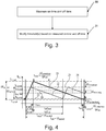
- Fig. 3 is a flow chart illustrating a method according to some embodiments. The method of Fig. 3 may be executed using the current mode switching regulator controllers and current mode switching regulators shown in Figs. 1A and 1B or as explained in more detail further below, but may also be used independently therefrom.
- the method of Fig. 3 comprises measuring an on-time t on and an off-time t off of a current mode switching regulator, for example based on comparator outputs as explained with reference to Figs. 1B and 2 .
- the method comprises modifying thresholds (for example Ihi and Ilow of Fig. 2 ) based on the measured on-time and off-time.
- the correction of thresholds may be based on further variables, for example inductance L of inductor 18 of Fig. 1B , input voltage V in in Fig. 1B , an estimation of the loop delay of the control loop or overshoot and undershoot times and slew rates, which may be measured. Examples for such approaches will now be discussed referring to Figs. 4 to 7 .
- Fig. 4 is a graph including example signals corresponding to curve 22 (ideal behavior) and 23 (example real behavior already discussed with reference to Fig. 2 ), where a plurality of quantities is illustrated which will be used in the following.
- I hi,ideal and I low,ideal are the threshold values according to lines 20 and 21, where for the ideal case the current according to curve 22 has its maximum and minimum, respectively.
- I hi,real and I low,real are the corresponding maximum and minimum values for the example real curve 23 including undershoots and overshoots.
- the difference between I hi,ideal and I low,ideal i.e. the current swing in the ideal case according to curve 22, is ⁇ I pp,ideal
- the corresponding value for curve 23 is ⁇ I pp,real.
- ⁇ I overshoot is the difference between I hi,real and I hi,ideal
- ⁇ I undershoot is the difference between I lo,ideal and I lo,real .
- ⁇ I error,avg is the difference between the average current for curve 22 I avg,ideal , which is (I hi,ideal +I lo,ideal ) /2, and I avg,real , which is the average current for curve 23.
- a time between curve 23 reaching I hi,real and then falling to I hi,ideal is named t over , and a time between curve 23 reaching I low,real , and then reaching I lo,ideal is named t under .
- t over ⁇ I overshoot /SR off
- t under ⁇ I undershoot /SR on .
- SR on is the Slew rate (i.e. slope) of the current when the supply stage is switched on
- SR off is the slew rate of the current when the supply stage is switched off.
- the error depends on duty cycle, input voltage, inductance L and the loop delay.
- the error ⁇ I error,avg may be calculated based on t off and t on , as explained above.
- the inductance L is known by design of the current mode switching regulator.
- the input voltage V in is either known for a specific setup or may be measured.
- comparators may be provided comparing the input voltage V in with threshold values, such that a range in which the input voltage V in lies is determined. In other embodiments, more precise measurements of the input voltage V in may be performed, for example using an analog-to-digital converter. If the regulator is used for a specific input voltage, this may also be programmed into a controller like controller 10 or controller 15.
- the loop delay ⁇ loop may at least be approximated. For example, typical loop delays are between 80 ns and 120 ns.
- the loop delay may be also determined at least in part by circuit simulations. For example, the part of the loop delay caused by a controller (controller 10 or controller 15) may be determined by circuit simulations, and the remaining loop delay may be estimated based on the line length and components used.
- the threshold values may be modified. For example, in some embodiments this error value may be essentially subtracted from the threshold values.
- the error values may also be calculated in terms of adjustable least significant bits (LSBs) of the threshold values.
- LSBs adjustable least significant bits
- the constant prefactor S comp,LSB is fixed for a certain setting (certain V in , L, and ⁇ loop caused by circuit design), and the value ⁇ I error,avg,LSB may be calculated based on t on and t off .
- the multiplication with s comp,LSB may be implemented by some simple shift operations in some embodiments. Also, the calculation (t off -t on ) / (t on +t off ) in usual applications is not time-critical, as the values in many applications do not vary rapidly.
- an averaging of one or more of t on , t off , (t off -t on ) / (t on +t off ), or ⁇ I error,avg,LSB may be applied, for example over a plurality of on-times and off-times.
- Fig. 5 illustrates a current mode switching regulator controller operating based on equation (13) above according to an embodiment and in particular the error calculation part thereof.
- Other parts for example for driving a supply stage like supply stage 11 or the supply stage in Fig. 1B , may be implemented for example as shown in Fig. 1B with driver 112 or in any conventional manner.
- the controller shown in Fig. 5 comprises the threshold detection part 50 which has already been described with Fig. 1B .
- the outputs of comparators 52, 54 are also provided to a digital part 55 of the controller, specifically two counters 57, 58 of a measurement part 56.
- Counters 57, 58 are clocked by a clock signal provided by an oscillator 59. This may be a clock signal clocking digital part 55.
- Counter 57 counts during t on , i.e. start of counting is triggered by the voltage CS+ reaching the lower current threshold from above (as detected by comparator 54) and stopped when the voltage at CS+ reaches the upper current threshold from below, as detected by comparator 52.
- counter 58 measures t off and is started when the voltage indicated by CS reaches the upper threshold from below (as indicated by comparator 52) and stopped when the voltage reaches the lower current threshold from above (as indicated by comparator 54). Therefore, the counting value of counter 57 is representative of t on , and the counting value of counter 58 is representative of t off .
- the clock frequency in embodiments is greater than the switching frequency for example at least ten times greater or at least 50 times greater, for example about a factor of 100 greater, to allow corresponding precise measurements of t on and t off .
- computation unit 511 calculates (t off -t on ) / (t on + off ) used in equation (13). This value is then multiplied with the scaling factor s comp,LSB in a multiplier 520. s comp,LSB is provided from a storage 512.
- Storage 512 may for example comprise a look-up table where s comp is pre-calculated and stored for a plurality of values or value ranges for input voltage V in , L and ⁇ loop and is selected accordingly. As mentioned above, these values ⁇ loop , V in , L are known by design, application scenario or may be measured. In embodiments where a certain controller is to be used for a certain setting (certain input voltage, certain inductance L) and this is known in advance, also only the single appropriate factor s comp,LSB for these particular settings may be programmed into storage 512, for example by using a voltage across a resistor coupled to a pin of the controller.
- a current error compensation part 513 values based on the correction value ⁇ I error,avg,LSB output for multiplier 520 are subtracted or added by subtractors 518, 519 from or to a nominal lower current threshold stored in a storage 514 and a nominal upper current threshold stored in a storage 516, to result in corrected values stored in storages 515, 517, respectively. Whether a subtraction or addition may be used may depend on the sign convention and calculation of ⁇ I error,avg,LSB .
- values may be subtracted (mathematically, such that subtraction of a negative value corresponds to an addition) from the nominal upper and lower thresholds to lower them for a positive ⁇ I error,avg,LSB .
- values may be added to the nominal upper and lower thresholds. For example, the correction value ⁇ I error,avg,LSB may be subtracted from or added to both the nominal upper and lower threshold current.
- ratios are also possible, for example such that in embodiments rv ⁇ I error,avg,LSB may be subtracted from the nominal lower threshold current and (2-rv) ⁇ I error,avg,LSB may be subtracted from the nominal upper threshold current, where rv is a value between 0 and 2.
- rv is a value between 0 and 2.
- multiplicative correction factors for the nominal upper and lower threshold currents may be derived from ⁇ I error,avg,LSB .
- Storages 514 to 517 may be registers, memory cells, or any other part within digital part 554 allowing the calculations explained. These corrected values are then fed to digital-to-analog converters 51, 53 to be used (in analog converted versions) as upper and lower current thresholds in comparators 52, 54. In this way, in some embodiments an effect of the loop delay, in particular on the average current, may be significantly reduced, depending on implementation.
- Table 1 Inductor Size L in ⁇ H Error of Average Current in LSBs Using Predictive Error Correction Error of Average Current in LSBs Without Any Correction (original) V in,lo ( ⁇ 40V) V in,mid (40V-80V) V in,hi ( ⁇ 80V) V in,hi,2 ( ⁇ 90V) V in,lo ( ⁇ 40V) V in,mid (40V-80V) V n,hi ( ⁇ 80V) V in,hi,2 ( ⁇ 90V) 640-1000 +/-1,38 +/- 2,55 +/- 2,13 +/- 2,76 +/- 2,3 +/- 4,55 +/- 5,13 +/- 5,76 470-640 +/-2,14 +/- 2,58 +/- 2,48 +/- 2,49 +/- 3,14 +/- 6,2 +/- 6,98 +/- 7,84 400-470 +/-2,32 +/- 2,92 +/- 2,38 +/- 2,43 +/- 3,69 +/-
- the table 1 gives the average current error in least significant bits. As can be seen, the current error may be reduced significantly, for example may be approximately halved in many cases down to low single digit LSBs.
- the current error generally also depends on the duty cycle, where it is generally close to 0 at a duty cycle of 0.5 and increases for higher duty cycles. A reduction of the current error was observed over a wide range of duty cycles.
- Fig. 6 shows the already discussed curve 23 representing an example for a real current behavior, together with line 20 representing the lower current threshold and line 21 representing the upper current threshold.
- both the lower current threshold as represented by line 20 are crossed twice (at 61, 62, and then 65, 66 in a next period T) and the upper current threshold as represented by line 21 is also crossed twice (at 63 and 64).
- Each crossing of the lower current threshold and the upper current threshold may be detected for example with the respective comparator (for example comparators 52, 54 of Fig. 1B ) by a state change of the respective output. Therefore, additional times may be measured by monitoring the change of the comparator outputs.
- a rise time t rise from the current crossing the lower current threshold from below (for example at 62) to the current reaching the upper current threshold (for example at 63), an overshoot time t m,hi , between the crossings of the upper current threshold in a period (for example between 63 and 64 of Fig. 6 ), a fall time t fall , between the current crossing the upper current threshold from above (for example at 64) and the current crossing the lower current threshold from above (for example at 65 in Fig. 6 ), and an undershoot time t m,low , between the crossings of the lower current threshold delimiting an undershoot (for example between 61 and 62 in Fig. 6 or between 65 and 66 in Fig. 6 ).
- the slew rate SR on may be expressed by ⁇ I pp (for example expressed in terms of least significant bits) and t rise
- slew rate SR off may be expressed using ⁇ I pp and t fall . This will be explained in more detail below.
- V in /L may be determined based on the slew rate SR on and SR off for the rising and falling portions of the load current, respectively, and the difference of the selected (i.e. ideal) threshold levels, named ⁇ I pp,LSB (corresponding to ⁇ I pp,ideal of Fig. 4 ).
- ⁇ I pp,LSB the difference of the selected (i.e. ideal) threshold levels
- V in /L may therefore be calculated by measuring t rise and t fall .
- ⁇ loop may be calculated by measuring t m,hi and/or t m,low , i.e. the times where the current is above the upper threshold value or below the lower threshold value. Using equations (7) and (8) as well as the relationships shown in Figs. 4 and 6 , ⁇ loop may be calculated as follows.
- SR on and SR off as explained above may also be determined based on t fall and t rise (see Fig. 6 ). Therefore, ⁇ loop may be measured using t m,lo or t m,hi .
- ⁇ loop may be calculated both by measuring t m,hi and t m,lo .
- one of these times may be very short (for example, in Fig. 6 t m,lo is much shorter than t m,hi ).
- a digital clock similar to the measurement using counters and oscillator 59 in Fig. 9
- such a short time may be only very few clock cycles of this clock if it becomes short, which may lead to a comparatively large measurement error (as in such measurements the clock cycle is the shortest unit).
- both t m,hi and t m,lo are measured, and an average may be made according to the below equation (18).
- ⁇ loop 1 2 ⁇ t m , hi ⁇ SR off SR off + SR on + t m , lo ⁇ SR on SR off + SR on
- both t m,hi and t m,lo may be measured and compared for each other, and for calculating ⁇ loop only the larger of the two times may be used, i.e. either equation (16) or equation (17) is used. In still other embodiments, only t m,hi or only t m,lo may be used.
- Fig. 7 illustrates a part of a controller implementing such an approach.
- the controller of Fig. 7 comprises the already discussed threshold detection circuit 50, oscillator 59 and a digital part 70.
- Timing measurement part 71 in the embodiment of Fig. 7 comprises six counters clocked by a clock supplied by oscillator 59. Each counter measures one of the times explained above with reference to Figs. 4 and 6 , by starting and stopping to count at the respective state changes of the output signals of comparators 52, 54, which correspond to the current crossing the upper or lower threshold value.
- a counter 72 measures t fall
- a counter 73 measures t rise
- a counter 74 measures t m,lo
- a counter 75 measures t m,hi
- a counter 76 measures t on and a counter 77 measures t off .
- the number of counters may vary depending on implementation. For example, while separate counters are shown in Fig. 7 for each time to be measured, different times may also be measured by a single counter sequentially.
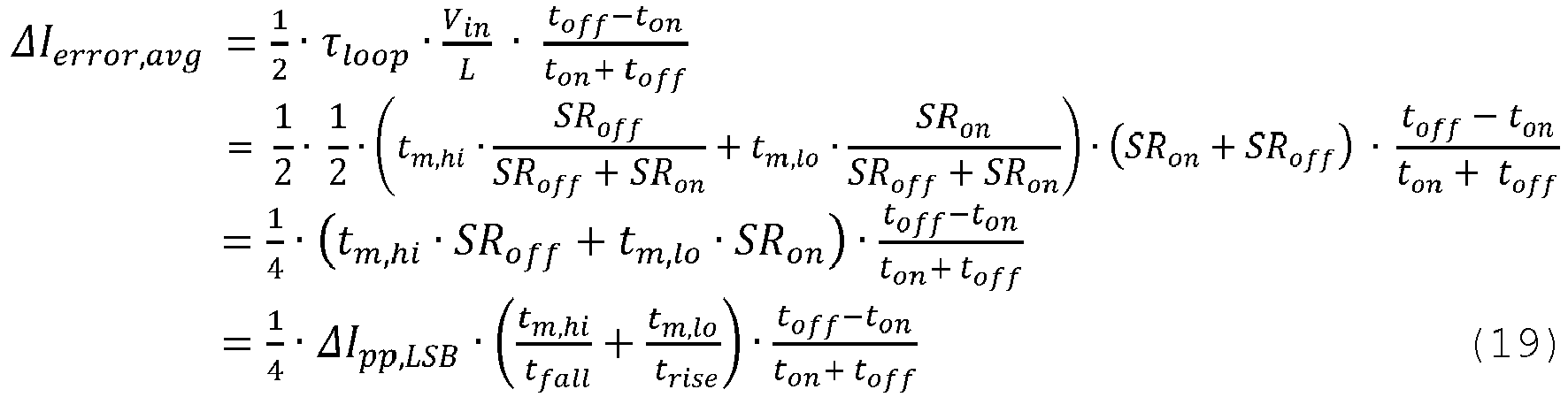
- a current error computation part 78 determines a correction value according to equation (19).
- This calculation is symbolized by elements 79, 710 to 713 in Fig. 7 . These elements merely symbolize the calculation, and the calculation may be implemented in any manner. In particular, these elements represent the calculation of the various factors of equation (19).
- the slew rates ⁇ I pp,LSB /t rise and ⁇ I pp,LSB /t fall are calculated, which are then used to calculate V in / L at 710 and ⁇ loop at 711.
- the duty cycle value (1-2D) is calculated according to (t off -t on ) / (t on +t off ). All these elements are multiplied by 1/4 (713) to result in ⁇ I error,avg .
- a compensation part 513 essentially corresponds to the compensation part 513 of Fig. 5 , where now the values based on ⁇ I error,avg calculated in part 78 are subtracted at subtractors 518, 519.
- the current error may be further reduced, in some cases by a further factor of 2.
- the approach of the embodiment of Fig. 5 may be more precise, for example when the loop delay, the inductance of the inductor and the input voltage is known precisely.
- the clock frequency used for timing measurement has an impact of the precision of the measurements of the various times and hence on the precision, and for the embodiment of Fig. 5 clock requirements may be more relaxed.
- Fig. 8 illustrates a current mode switching regulator according to an embodiment, which may use a controller using a compensation for loop delay as discussed with reference to Fig. 5 or Fig. 7 . While Fig. 8 shows a specific implementation, this serves only as illustrative example, and as already mentioned techniques disclosed herein may be used in conjunction with various topologies.
- a controller 80 is provided to control a supply stage including transistor 16, diode 17 and inductor 18 which have already been discussed referring to Fig. 1B . Additionally, a bootstrap capacitor 85 is provided in the implementation example of Fig. 8 . Similar to Fig. 1B , in the embodiment of Fig. 8 a chain of light-emitting diodes 19 is supplied with current. The current through the diodes is measured using the already discussed shunt resistor 110.
- the measured current is provided to controller 80 at terminals CS+, CS- and are compared with an upper current threshold and a lower current threshold using the already discussed threshold detection circuit 50.
- Outputs of the comparators (52 and 54) of threshold detection circuit 50 are provided to a digital current error determination and compensation part 83, which may be implemented corresponding to parts 56, 510, 512 and 513 of Fig. 5 or implemented corresponding to parts 71, 78 and 513 of Fig. 7 to set the threshold values for threshold detection circuit 50.
- an analog pulse control part 82 of an analog part 81 which may for example comprise logic gates, flip-flops, latches, filters and other elements to provide a pulse with modulated voltage V PWM , which is then used to drive transistor 16 through driving circuitry 84.
- Driving circuitry 84 in the example of Fig. 8 uses a low-side transistor M1 and a high-side transistor M2 driven by respective drivers to output a signal to the gate of transistor 16 at a terminal HSGD. Any conventional driving circuitry 84 and pulse control circuitry 82 may be used, and the implementation shown is merely an example.
- Fig. 8 While a certain topology for supply stage and kind of the supply stage based on the threshold crossings is shown in Fig. 8 , the approaches discussed herein may generally be used in circuits like switched mode power supply where an output current is regulated based on an upper threshold and a lower threshold.
- techniques discussed herein are not applicable to current control only, but are generally applicable to cases where an output quantity is regulated based on upper and lower thresholds.
- Examples include voltage regulations or temperature regulations.
- a voltage divider like a resistive divider may be coupled in parallel to a load to provide a feedback signal indicative of a voltage across the load, which may then be compared to upper and lower voltage thresholds.
Landscapes
- Engineering & Computer Science (AREA)
- Power Engineering (AREA)
- Dc-Dc Converters (AREA)
Abstract
Description
- The presented application relates to current mode switching regulator controllers, current mode switching regulators comprising such controllers and to corresponding methods.
- Current mode switching regulators are used in some applications to supply a current to a load. For example, such regulators may be used to supply light-emitting diodes (LEDs) with current.
- Generally, such regulators measure the current through the load. When the current reaches an upper current threshold, a supply stage supplying current to the load is switched off, and when the current then reaches a lower current threshold, the supply stage is switched on again. This may lead to a sawtooth-like current between the upper and the lower current threshold through the load, with an average current, which in an ideal case is an average value of the upper and the lower current threshold.
- However, for the control loop which uses the upper and the lower current threshold explained above, a certain loop delay exists, due to the signal propagation from a device measuring the load current (for example a shunt resistor) to a controller, through the controller and from there to the supply stage. This loop delay may lead to overshoots and undershoots, i.e. the load current exceeding the upper current threshold or falling below the lower current threshold. These over- and undershoots may also affect the average current supplied to the load, which is undesirable in applications like LED driving which require very precise currents.
- The current overshoot and undershoot and therefore the error of the average current also depends on a duty cycle of the regulation (for example the frequency of the above-mentioned sawtooth-like current curve) and therefore is not a fixed quantity of a given system, but may change during operation.
- Some recent solutions to this problem use elaborate regulation and control techniques, which require very precise measurements of one or more parameters like the actual current flow or a voltage of a pin of a controller used to control the switching. Such solutions come at the cost of higher hardware effort, complexity and slower reaction times.
- A controller as defined in
claim 1 and a method as defined inclaim 13 are provided. The dependent claims define further embodiments as well as a current mode switching regulator including such a controller. - According to an embodiment, a controller is provided, comprising:
- a threshold detection circuit configured to receive a feedback signal indicative of a load current, and to detect when the load current reaches an upper current threshold or a lower current threshold,
- a control circuit configured to control a supply stage in response to the detecting to supply a load with the load current, and
- a current error determination and compensation circuit configured to determine an on-time between a first point in time, where the load current reaches the lower threshold current from above, and a second point in time, where the load current reaches the upper current threshold from below, and an off-time between the second point in time and a following first point in time, and to adjust the upper current threshold and the lower current threshold based on the on-time and the off-time.
- According to another embodiment, a method is provided, comprising:
- receiving a feedback signal indicative of a load current,
- detecting when the load current reaches an upper current threshold or a lower current threshold,
- driving a supply stage in response to the detecting to supply a load with the load current,
- determining an on-time between a first point in time, where the load current reaches the lower threshold current from above, and a second point in time, where the load current reaches the upper current threshold from below, and an off-time between the second point in time and a following first point in time, and
- adjusting the upper current threshold and the lower current threshold based on the on-time and the off-time.
- The above summary is merely a brief overview over some embodiments and is not to be construed as limiting in any way, as other embodiments may include other features than the ones listed above.
-
-
Fig. 1A is a block diagram of a current mode switching regulator according to an embodiment. -
Fig. 1B is a diagram illustrating a current mode switching regulator according to an embodiment. -
Fig. 2 is a graph for explaining current overshoot and undershoot, the effects of which are mitigated in some embodiments. -
Fig. 3 is a flow chart illustrating a method according to an embodiment. -
Fig. 4 is a diagram illustrating various quantities used for explanation of embodiments. -
Fig. 5 is a diagram of a controller according to an embodiment. -
Fig. 6 is a diagram for illustrating further measurements used in some embodiments. -
Fig. 7 is a diagram of a controller according to an embodiment. -
Fig. 8 is a diagram of a current mode switching regulator according to a further embodiment. - In the following, various embodiments will be described in detail referring to the attached drawings. These embodiments serve illustrative purposes only and are not to be construed as limiting. For example, while embodiments may be described comprising a plurality of features (for example components, elements, acts, events, steps etc.), in other embodiments some of these features may be omitted, and/or may be replaced by alternative features. In addition to the features explicitly shown and described, other features, for example features used in conventional current mode switching regulators, may be provided. For example, some of the embodiments described herein relate to the compensation of current errors caused by a loop delay of a regulation, and apart from such techniques, regulators may be implemented in a conventional manner.
- Features described with respect to different embodiments may be combined unless noted otherwise. For example, some variations, modifications or details may be described only with respect to one of the embodiments in order to avoid repetitions, but may also be applied to other embodiments.
- Connections or couplings shown in the drawings or described herein refer to electrical connections or couplings unless noted otherwise. Such connections or couplings may be modified, for example by adding additional intervening elements or by removing elements, as long as the general purpose of the connection or coupling, for example to provide or transmit a certain kind of signal, to provide a control, to transmit a certain information etc. is essentially maintained.
- Throughout the figures, corresponding elements bear the same reference numerals and will not be described repeatedly.
- Turning now to the figures,
Fig. 1A is a block diagram of a current mode switching regulator according to an embodiment. The embodiment ofFig. 1A comprises acontroller 10 that controls asupply stage 11.Supply stage 11 provides a current to aload 12. A feedback signal fb indicative of the current through the load is fed back tocontroller 10. Feedback signal fb may be generated by any suitably circuitry, for example current sensing circuitry. In athreshold detection part 13 ofcontroller 10, the current through the load as indicated by the feedback signal fb is compared with an upper current threshold and a lower current threshold. Essentially, when the current exceeds the upper current threshold,supply stage 11 is switched off. Furthermore, when the current through the load falls below the lower current threshold,supply stage 11 is switched on. - In this way, the current through the
load 12 may be regulated. - Without further measures, the control loop established through the feedback signal fb and
controller 10 controllingsupply stage 11 in response to the feedback signal introduces a loop delay, which may lead to overshoots and undershoots. - In embodiments,
controller 10 comprises atime measurement part 14 for measuring an on-time ton of thesupply stage 11 and an off-time toff of thesupply stage 11. The on-time and the off-time may be measured based on the threshold detection inthreshold detection part 13. It should be noted that while the actual switching ofsupply stage 11 through the loop delay may be later than the actual exceeding of the upper current threshold, and likewise the switching on again due to the loop delay may be later than the actual falling below of the current through the load below the lower current threshold, as the loop delay is the same in both cases, the on- and off-times may still be measured essentially without influence of the loop delay. Based on the measured on- and off-times, the control is modified to compensate for overshoots and undershoots caused by the loop delay, for example by modifying the upper current thresholds and lower current thresholds used from their nominal values. Detailed examples for this kind of compensation will be explained further below. -
Controller 10 may be a controller comprising analog and digital parts. Completely analog or completely digital implementations are also possible in some embodiments. For example, thethreshold detection part 13 may be performed using at least some analog circuitry, for example comparators for comparing voltages or currents. In other embodiments, where the feedback signal fb is provided as a digital signal using e.g. a sufficiently fast analog to digital converter in a current sensing circuitry,threshold detection part 13 may be implemented digitally. The time measurement part may be implemented using digital circuitry, for example digital counters. A calculation of compensation values for the upper and lower current thresholds may then also be performed digitally. - To achieve this,
controller 10 may be implemented in any suitable manner. For example, a digital part ofcontroller 10 may be implemented using a digital signal processor, an application specific integrated circuit, a microcontroller, a microprocessor or similar devices, which allow digital calculations, counting and other digital signal processing. Analog portions may be implemented using digital-to-analog converters, analog comparators or other analog circuitry like transistor drivers outputting a driving signal forsupply stage 11. In other embodiments, such drivers may be external tocontroller 10, andcontroller 10 may only comprise the control circuit (for example implemented digitally) to control such drivers. Generally, describing or defining a controller as comprising different parts or circuits is to be understood as the controller including parts of circuits providing the respective functions, but does not imply that the parts or circuits are implemented as physically separate blocks. For example, various parts or circuits may be implemented by programming a microcontroller or other digital device accordingly. Some examples will be discussed next referring toFig. 1B . -
Fig. 1B illustrates a current mode switching regulator according to an embodiment. The current mode switching regulator ofFig. 1B is used to supply a chain of light-emitting diodes 19_1..., 19_n with power. Light-emitting diodes 19_1..., 19_n will be collectively referred to as light-emittingdiodes 19 in the following. While two light-emittingdiodes 19 are explicitly shown inFig. 1B , the chain of light-emitting diodes may comprise a higher number of light-emitting diodes. - The embodiment of
Fig. 1B furthermore comprises acontroller 15, which controls a supply stage comprising atransistor 16, adiode 17 and aninductor 18. Whentransistor 16 is turned on bycontroller 15, light-emittingdiodes 19 are coupled to a supply voltage Vin viainductor 18. Whentransistor 16 is switched off,inductor 18 and light-emittingdiodes 19 are decoupled from voltage Vin. Nevertheless, still a current may flow for some time e.g. due to energy stored ininductor 18. The configuration ofFig. 1B is only an example, and other conventional supply stages and current mode controlled converter topologies including synchronous and asynchronous converters may also be used. For example, for a synchronousbuck converter diode 17 may be replaced by further transistor acting as a switch controlled bycontroller 15, or even more transistors (e.g. 4 transistors for a synchronous buck-boost converter) may be used. In this respect, "switching off the supply stage" generally refers to stopping providing power from a supply voltage to the output, and "switching on the supply stage" refers to starting providing power from a supply voltage to the output, and may involve various switching schemes of a plurality of transistors of a supply stage. - A current ILED flowing through light-emitting
diodes 19, which is an example for a load current, is measured using ashunt resistor 110 having a resistance value Rcs. A voltage drop acrossshunt resistor 110 is indicative of the current ILED and is an example for feedback signal fb ofFig. 1A . The voltage acrossresistor 110 is supplied tocontroller 15 at terminals CS+, CS-. -
Controller 15 comprises a signal processing and controlpart 111, which may be implemented using digital circuitry, as explained above forcontroller 10 ofFig. 1A . Signal processing and controlpart 111 provides an upper current threshold value to a digital-to-analog converter 51 and a lower current threshold value to a digital-to-analog converter 53 of athreshold detection circuit 50, which is an example forthreshold detection part 13 ofFig. 1A . - An output of digital-to-
analog converter 51 is provided to a reference input of acomparator 52, and an output of digital-to-analog converter 53 is provided to a reference input of acomparator 54. The voltage at CS+ is provided to sensing inputs ofcomparators threshold detection circuit 50. In other implementations, other connections schemes are possible, e.g. using the voltages at CS+, CS- as differential signals. - Based on threshold crossings detected by
comparators part 111 controls adriver 112 to switchtransistor 16 on and off. Namely, if the current ILED exceeds the upper threshold current,transistor 16 is switched off, and when the current ILED falls below the lower threshold current,transistor 16 is switched off. - Specifically, when the load current as indicated by the voltage at CS+ crosses the voltage output from digital-to-
analog converter 51, an output signal ofcomparator 52 changes its state (for example from logic 0 tologic 1 or vice versa). When the voltage at CS+ crosses the output voltage of digital-to-analog converter 53,comparator 54 changes its output states. In this way, it may be detected when the current ILED exceeds the upper threshold current or falls below the lower threshold current. - Furthermore, based on the output of
comparators part 111 measures the above-mentioned values of ton and toff and modifies the threshold values supplied to digital-to-analog converters loop controlling transistor 16 based on the current ILED may be reduced in some embodiments. - The on-time ton, the off-time toff as well as the overshoots and undershoots due to the above-mentioned loop delay of the control loop are further illustrated in
Fig. 2 . -
Fig. 2 generally shows the LED current ILED over time. Furthermore, an upper current threshold Ihi is indicated by aline 21, and a lower current threshold Ilow is indicated by aline 20. - A
curve 22 illustrates the ideal behavior of the current in this case. When the current reaches line 20 from higher currents, a supply stage likesupply stage 11 ortransistor 16 inFigs. 1A and 1B is switched on, and the current rises, and as soon as the current reachesline 21, the supply stage is switched off again, and the current falls. - This leads to an average current of (Ihi+Ilow)/2 between Ihi and Ilow as indicated by
line 24 inFig. 2 . - Due to the loop delay of the control loop, the real behavior of the current differs from the ideal behavior. A
curve 23 inFig. 2 shows an example for such a real behavior. As the load current ILED reaching the upper threshold current Ihi is detected only with a certain delay (for example signal time fromresistor 110 viathreshold detection circuit 50 to signal processing and controlpart 111 inFig. 1B ) and then the supply stage is switched off with another delay (delay from signal and processing and controlpart 111 todrivers 112 andtransistor 16, for example), the current actually continues to rise for a bit after reachingline 21, leading to overshoots. For similar reasons, it continues to fall for a bit after reachingline 20, leading to undershoots. In the example ofFig. 2 , the overshoots are larger than the undershoots. In other cases, this may be different. In particular, the undershoots and overshoots depend on parameters including the duty cycle, inductance ofinductor 18, input voltage Vin, output voltage Vout and the loop delay. Therefore, the curves inFig. 2 are to be taken only as an illustrative example. The overshoots and undershoots lead to a shift of the average current, in this case to a higher value as indicated by aline 25 inFig. 2 . - In embodiments, an on-time ton and an off-time toff is measured. The on-time ton is the time between the current falling below Ilow and the current rising above Ihi, and the off-time toff is the time from the current rising above Ihi to falling below Ilow, as indicated in
Fig. 2 . While the crossings of Ihi and Ilow are detected with a certain delay as explained above, this delay is essentially the same for the crossing of Ihi and the crossing of Ilow. Therefore, the measurement of the on-time ton and the off-time toff is essentially not influenced by the loop delay of the control loop, as they correspond to the difference between two threshold crossings. Based on ton and toff, in embodiments then the threshold values Ihi and Ilow are modified to compensate for the loop delay. Examples for this compensation will be explained further below. - Before going into detail regarding the compensation of the threshold values, a method according to some embodiments will be described.
Fig. 3 is a flow chart illustrating a method according to some embodiments. The method ofFig. 3 may be executed using the current mode switching regulator controllers and current mode switching regulators shown inFigs. 1A and 1B or as explained in more detail further below, but may also be used independently therefrom. - At 30, the method of
Fig. 3 comprises measuring an on-time ton and an off-time toff of a current mode switching regulator, for example based on comparator outputs as explained with reference toFigs. 1B and2 . - At 31, the method comprises modifying thresholds (for example Ihi and Ilow of
Fig. 2 ) based on the measured on-time and off-time. As will be explained further below, in addition to the on-time and off-time, the correction of thresholds may be based on further variables, for example inductance L ofinductor 18 ofFig. 1B , input voltage Vin inFig. 1B , an estimation of the loop delay of the control loop or overshoot and undershoot times and slew rates, which may be measured. Examples for such approaches will now be discussed referring toFigs. 4 to 7 . -
Fig. 4 is a graph including example signals corresponding to curve 22 (ideal behavior) and 23 (example real behavior already discussed with reference toFig. 2 ), where a plurality of quantities is illustrated which will be used in the following. Ihi,ideal and Ilow,ideal are the threshold values according tolines curve 22 has its maximum and minimum, respectively. Ihi,real and Ilow,real are the corresponding maximum and minimum values for the examplereal curve 23 including undershoots and overshoots. The difference between Ihi,ideal and Ilow,ideal, i.e. the current swing in the ideal case according tocurve 22, is ΔIpp,ideal, and the corresponding value forcurve 23 is ΔIpp,real. - For
curve 22, the on- and off-times are denoted ton,ideal and toff,ideal, and forcurve 23 they are denoted ton,real and toff,real. The loop delay of the control loop is denoted τloop . - The sum of ton and toff is the switching period T, which is the inverse of the switching frequency fsw. For
curve 22, these are named Tideal and fsw,ideal, respectively, and forcurve 23 they are named Treal and fsw,real, respectively. - ΔIovershoot is the difference between Ihi,real and Ihi,ideal, and ΔIundershoot is the difference between Ilo,ideal and Ilo,real.
- ΔIerror,avg is the difference between the average current for curve 22 Iavg,ideal, which is (Ihi,ideal+Ilo,ideal) /2, and Iavg,real, which is the average current for
curve 23. - A time between
curve 23 reaching Ihi,real and then falling to Ihi,ideal is named tover, and a time betweencurve 23 reaching Ilow,real, and then reaching Ilo,ideal is named tunder. tover= ΔIovershoot/SRoff, and tunder= ΔIundershoot/SRon. SRon is the Slew rate (i.e. slope) of the current when the supply stage is switched on, and SRoff is the slew rate of the current when the supply stage is switched off. - It should be noted that the actual slew rates of
curve 23 depend on the applied duty cycle, where steeper slew rates result in higher overshoots or undershoots, whereas flatter slew rates result in smaller overshoots and undershoots. For a 50 % duty cycle ΔIerror,average would be at or near 0, as in this case the undershoot and overshoot would be equal. The duty cycle will be denoted D in the following. As seen inFig. 4 , the loop delay τloop and the under- and overshoots associated with this also extend the period T and therefore reduce the switching frequency fsw. - For the various quantities shown in
Fig. 4 , the following equations apply, where L is the inductance of an inductor of the supply stage,e.g. inductor 18 ofFig. 1B :


- The resulting error in the average voltages ΔIerror,avg may then be calculated according to

- As can be seen, the error depends on duty cycle, input voltage, inductance L and the loop delay.
- Inserting equation (2) into equation (11) to calculate the duty cycle based on ton and toff results in

- Therefore, as can be seen, the error ΔIerror,avg may be calculated based on toff and ton, as explained above.
- Furthermore, in equation (12), the inductance L is known by design of the current mode switching regulator. The input voltage Vin is either known for a specific setup or may be measured. For example, comparators may be provided comparing the input voltage Vin with threshold values, such that a range in which the input voltage Vin lies is determined. In other embodiments, more precise measurements of the input voltage Vin may be performed, for example using an analog-to-digital converter. If the regulator is used for a specific input voltage, this may also be programmed into a controller like
controller 10 orcontroller 15. The loop delay τloop may at least be approximated. For example, typical loop delays are between 80 ns and 120 ns. The loop delay may be also determined at least in part by circuit simulations. For example, the part of the loop delay caused by a controller (controller 10 or controller 15) may be determined by circuit simulations, and the remaining loop delay may be estimated based on the line length and components used. - Therefore, at least a good approximation of the values Vin, L, τloop may be provided and a corresponding estimate for ΔIerror,avg may be calculated. Based on this error, then the threshold values may be modified. For example, in some embodiments this error value may be essentially subtracted from the threshold values.
- For digital processing, for example digital providing of the error values by signal processing and control
part 111 ofFig. 1B to digital-to-analog converters 
- The constant prefactor Scomp,LSB is fixed for a certain setting (certain Vin, L, and τloop caused by circuit design), and the value ΔIerror,avg,LSB may be calculated based on ton and toff. The multiplication with scomp,LSB may be implemented by some simple shift operations in some embodiments. Also, the calculation (toff-ton) / (ton+toff) in usual applications is not time-critical, as the values in many applications do not vary rapidly. In some embodiments, also an averaging of one or more of ton, toff, (toff-ton) / (ton+toff), or ΔIerror,avg,LSB may be applied, for example over a plurality of on-times and off-times.
-
Fig. 5 illustrates a current mode switching regulator controller operating based on equation (13) above according to an embodiment and in particular the error calculation part thereof. Other parts, for example for driving a supply stage likesupply stage 11 or the supply stage inFig. 1B , may be implemented for example as shown inFig. 1B withdriver 112 or in any conventional manner. - The controller shown in
Fig. 5 comprises thethreshold detection part 50 which has already been described withFig. 1B . Apart from using the output ofcomparators transistor 16 ofFig. 1B , the outputs ofcomparators counters measurement part 56. - It should be noted that describing digital parts with a plurality of blocks (like
blocks Fig. 5 ) does not imply physically separate blocks, but may only indicate various functions that may be implemented using a digital part like a digital signal processor, ASIC, logic circuit or the like. -
Counters oscillator 59. This may be a clock signal clocking digital part 55. -
Counter 57 counts during ton, i.e. start of counting is triggered by the voltage CS+ reaching the lower current threshold from above (as detected by comparator 54) and stopped when the voltage at CS+ reaches the upper current threshold from below, as detected bycomparator 52. Conversely, counter 58 measures toff and is started when the voltage indicated by CS reaches the upper threshold from below (as indicated by comparator 52) and stopped when the voltage reaches the lower current threshold from above (as indicated by comparator 54). Therefore, the counting value ofcounter 57 is representative of ton, and the counting value ofcounter 58 is representative of toff. - It should be noted that to some extent the precision of this measurement of ton and toff also depends on the clock frequency of
clock 59, as the times ton, toff are measured in terms of clock cycles. Therefore, the clock frequency in embodiments is greater than the switching frequency for example at least ten times greater or at least 50 times greater, for example about a factor of 100 greater, to allow corresponding precise measurements of ton and toff. - The values for ton and toff thus obtained are provided to a
computation unit 511 of a currenterror prediction part 510. The calculations in currenterror prediction part 510 may be implemented in any suitable digital manner, and the representation ofFig. 5 is merely an example. As indicated by the "-", "+" and "÷" signs and the arrows there between,computation unit 511 calculates (toff-ton) / (ton+off) used in equation (13). This value is then multiplied with the scaling factor scomp,LSB in amultiplier 520. scomp,LSB is provided from astorage 512.Storage 512 may for example comprise a look-up table where scomp is pre-calculated and stored for a plurality of values or value ranges for input voltage Vin, L and τloop and is selected accordingly. As mentioned above, these values τloop , Vin, L are known by design, application scenario or may be measured. In embodiments where a certain controller is to be used for a certain setting (certain input voltage, certain inductance L) and this is known in advance, also only the single appropriate factor scomp,LSB for these particular settings may be programmed intostorage 512, for example by using a voltage across a resistor coupled to a pin of the controller. - In a current
error compensation part 513, values based on the correction value ΔIerror,avg,LSB output formultiplier 520 are subtracted or added bysubtractors storage 514 and a nominal upper current threshold stored in astorage 516, to result in corrected values stored instorages -
Storages 514 to 517 may be registers, memory cells, or any other part within digital part 554 allowing the calculations explained. These corrected values are then fed to digital-to-analog converters comparators - As can be seen in
Fig. 5 , most of the calculations may be performed digital, and thethreshold detection 50 is needed anyway for the control of the supply stage. Therefore, for implemented the current error compensation technique ofFig. 5 , minimum additional hardware is necessary, and essentially only digital calculations in a controller have to be implemented accordingly. - To illustrate the effect of the discussed current error compensation, the following two tables show results with techniques as discussed above and without them for different inductor sizes and input voltages. Loop delay has been varied from 80ns to 120ns for each set of Vin and L. Table 1 shows the effect in terms of LSBs (assuming 10 bit resolution of 1.3 A max. current and a digital clock frequency of 55 MHz; duty cycle variations from 10% to 90%), while table 2 shows the situation for a relative error in percent for the same simulation settings.
Table 1: Inductor Size L in µH Error of Average Current in LSBs Using Predictive Error Correction Error of Average Current in LSBs Without Any Correction (original) Vin,lo (≤ 40V) Vin,mid (40V-80V) Vin,hi (≥ 80V) Vin,hi,2 (≥ 90V) Vin,lo (≤ 40V) Vin,mid (40V-80V) Vn,hi (≥ 80V) Vin,hi,2 (≥ 90V) 640-1000 +/-1,38 +/- 2,55 +/- 2,13 +/- 2,76 +/- 2,3 +/- 4,55 +/- 5,13 +/- 5,76 470-640 +/-2,14 +/- 2,58 +/- 2,48 +/- 2,49 +/- 3,14 +/- 6,2 +/- 6,98 +/- 7,84 400-470 +/-2,32 +/- 2,92 +/- 2,38 +/- 2,43 +/- 3,69 +/- 7,28 +/- 8,2 +/- 9,22 370-400 +/-2,39 +/- 2,87 +/- 2,42 +/- 2,47 +/- 3,99 +/- 7,87 +/- 8,87 +/- 9,96 350-370 +/- 2,21 +/-3,34 +/- 2,37 +/- 2,86 +/- 4,21 +/- 8,32 +/- 9,37 +/- 10,53 310-350 +/-2,76 +/- 3,39 +/- 2,58 +/- 2,89 +/- 4,76 +/- 9,39 +/- 10,58 +/- 11,89 280-310 +/-3,27 +/- 3,81 +/- 3,13 +/- 3,17 +/- 5,27 +/- 10,4 +/- 11,72 +/- 13,17 230-280 +/-3,45 +/- 4,66 +/- 4,26 +/- 4,13 +/- 6,41 +/-12,66 +/-14,26 +/- 16,03 200-230 +/-4,37 +/- 5,54 +/- 4,06 +/- 4,95 +/- 7,37 +/- 14,56 +/- 16,4 +/- 18,43 180-200 +/-4,78 +/- 5,83 +/- 4,4 +/- 4,66 +/- 8,19 +/-16,18 +/-18,23 +/- 20,48 150-180 +/-5,83 +/- 7,42 +/- 5,87 +/- 6,58 +/- 9,83 +/- 19,42 +/- 21,87 +/- 24,58 130-150 +/-6,34 +/- 8,05 +/- 6,24 +/- 6,75 +/- 11,34 +/- 22,4 +/- 25,24 +/- 28,36 110-130 +/-7,41 +/- 9,94 +/- 7,83 +/- 8,31 +/- 13,41 +/- 26,48 +/- 29,83 +/- 33,51 90-110 +/-9,38 +/- 11,4 +/- 9,45 +/- 10,93 +/- 16,38 +/- 32,36 +/- 36,45 +/- 40,96 Table 2: Inductor Size L in µH Error of Average Current in % (for I LED =250mA) Using Predictive Error Correction Error of Average Current in % (for I LED =250mA) Without Any Correction (original) Vin,lo (≤ 40V) Vin,mid (40V-80V) Vin,hi (≥ 80V) Vin,hi,2 (≥ 90V) Vin,lo (≤ 40V) Vin,mid (40V-80V) Vin,hi (≥ 80V) Vin,hi,2 (≥ 90V) 640-1000 +/-0,72 +/- 1,33 +/- 1,11 +/- 1,44 +/- 1,2 +/- 2,37 +/- 2,67 +/- 3 470-640 +/-1,11 +/- 1,34 +/- 1,29 +/- 1,3 +/- 1,63 +/- 3,23 +/- 3,64 +/- 4,09 400-470 +/- 1,21 +/-1,52 +/- 1,24 +/- 1,27 +/- 1,92 +/- 3,79 +/- 4,27 +/- 4,8 370-400 +/-1,24 +/- 1,5 +/-1,26 +/-1,29 +/-2,08 +/-4,1 +/- 4,62 +/- 5,19 350-370 +/-1,15 +/- 1,74 +/- 1,24 +/- 1,49 +/- 2,19 +/- 4,33 +/- 4,88 +/- 5,49 310-350 +/-1,44 +/- 1,77 +/- 1,35 +/- 1,51 +/- 2,48 +/- 4,89 +/- 5,51 +/- 6,19 280-310 +/- 1,7 +/- 1,98 +/- 1,63 +/- 1,65 +/- 2,74 +/- 5,42 +/- 6,1 +/- 6,86 230-280 +/-1,8 +/- 2,43 +/- 2,22 +/- 2,15 +/- 3,34 +/- 6,59 +/- 7,43 +/- 8,35 200-230 +/- 2,28 +/- 2,89 +/- 2,12 +/-2,58 +/- 3,84 +/- 7,58 +/- 8,54 +/- 9,6 180-200 +/- 2,49 +/- 3,04 +/- 2,29 +/- 2,43 +/- 4,27 +/- 8,43 +/- 9,49 +/- 10,67 150-180 +/- 3,04 +/- 3,86 +/- 3,06 +/- 3,43 +/- 5,12 +/-10,11 +/- 11,39 +/- 12,8 130-150 +/- 3,3 +/- 4,19 +/- 3,25 +/- 3,51 +/- 5,91 +/- 11,67 +/- 13,14 +/- 14,77 110-130 +/- 3,86 +/- 5,18 +/- 4,08 +/- 4,33 +/- 6,98 +/- 13,79 +/- 15,53 +/- 17,45 90-110 +/- 4,89 +/- 5,94 +/- 4,92 +/- 5,7 +/- 8,53 +/- 16,85 +/- 18,99 +/- 21,33 - The table 1 gives the average current error in least significant bits. As can be seen, the current error may be reduced significantly, for example may be approximately halved in many cases down to low single digit LSBs.
- It should be noted that the current error generally also depends on the duty cycle, where it is generally close to 0 at a duty cycle of 0.5 and increases for higher duty cycles. A reduction of the current error was observed over a wide range of duty cycles.
- In the above embodiment, estimations or measurements of Vin, L and τloop . were necessary. Next, further embodiments will be discussed where additional time measurements are used to determine or estimate of Vin/L and τloop .
- The measurement of additional times is illustrated in
Fig. 6. Fig. 6 shows the already discussedcurve 23 representing an example for a real current behavior, together withline 20 representing the lower current threshold andline 21 representing the upper current threshold. - As can be seen, in each period T as defined with respect to
Fig. 4 , both the lower current threshold as represented byline 20 are crossed twice (at 61, 62, and then 65, 66 in a next period T) and the upper current threshold as represented byline 21 is also crossed twice (at 63 and 64). Each crossing of the lower current threshold and the upper current threshold may be detected for example with the respective comparator (forexample comparators Fig. 1B ) by a state change of the respective output. Therefore, additional times may be measured by monitoring the change of the comparator outputs. - These times are a rise time trise, from the current crossing the lower current threshold from below (for example at 62) to the current reaching the upper current threshold (for example at 63), an overshoot time tm,hi, between the crossings of the upper current threshold in a period (for example between 63 and 64 of
Fig. 6 ), a fall time tfall, between the current crossing the upper current threshold from above (for example at 64) and the current crossing the lower current threshold from above (for example at 65 inFig. 6 ), and an undershoot time tm,low, between the crossings of the lower current threshold delimiting an undershoot (for example between 61 and 62 inFig. 6 or between 65 and 66 inFig. 6 ). As also indicated inFig. 6 , the slew rate SRon may be expressed by ΔIpp (for example expressed in terms of least significant bits) and trise, and slew rate SRoff may be expressed using ΔIpp and tfall. This will be explained in more detail below. - Reverting to equation (12) the three contributors to the actual error may be seen as 1. (toff-ton) / (ton+toff), 2. Vin/L, and 3. τlοοp. As already explained above, (toff-ton) / (ton+toff) may be measured, for example as explained with reference to
Fig. 5 . With the additional measurements illustrated inFig. 6 , also the other two contributions (2. and 3.) may be determined, as shown in the following. - The contribution of Vin/L, as to some extent already indicated in
Fig. 6 , may be determined based on the slew rate SRon and SRoff for the rising and falling portions of the load current, respectively, and the difference of the selected (i.e. ideal) threshold levels, named ΔIpp,LSB (corresponding to ΔIpp,ideal ofFig. 4 ). Using equations (4) and (6) results in
- As ΔIpp,LSB is known as difference between the threshold voltage levels set by the controller, Vin/L may therefore be calculated by measuring trise and tfall.
- The contribution of τloop may be calculated by measuring tm,hi and/or tm,low, i.e. the times where the current is above the upper threshold value or below the lower threshold value. Using equations (7) and (8) as well as the relationships shown in
Figs. 4 and6 , τloop may be calculated as follows.
- SRon and SRoff as explained above may also be determined based on tfall and trise (see
Fig. 6 ). Therefore, τloop may be measured using tm,lo or tm,hi. - As seen from equation (16) and (17), τloop may be calculated both by measuring tm,hi and tm,lo. Depending on the duty cycle, one of these times may be very short (for example, in
Fig. 6 tm,lo is much shorter than tm,hi). When such times are measured using a digital clock (similar to the measurement using counters andoscillator 59 in Fig. 9), such a short time may be only very few clock cycles of this clock if it becomes short, which may lead to a comparatively large measurement error (as in such measurements the clock cycle is the shortest unit). To increase robustness, in some embodiments both tm,hi and tm,lo are measured, and an average may be made according to the below equation (18).
- In other embodiments, both tm,hi and tm,lo may be measured and compared for each other, and for calculating τloop only the larger of the two times may be used, i.e. either equation (16) or equation (17) is used. In still other embodiments, only tm,hi or only tm,lo may be used.
- The resulting error ΔIerror,avg using equations (12), (14) and (18) may be calculated according to
- Consequently, by measuring the times shown in
Fig. 6 , namely ton, toff, trise, tfall, tm,hi, and tm,lo, it is possible to calculate ΔIerror,avg without needing to make assumptions about or measurements of the input voltage Vin, the inductance L of an inductor used or the loop delay τloop . It should be noted that when using equation (19), the loop delay does not have to be determined beforehand or separately, but ΔIerror,avg may be calculated directly based on measured times. It should also be noted that in yet other embodiments, VIN/L may be determined based on equation (14), but τloop may be estimated as in the embodiment ofFig. 5 , or may be calculated separately as in equation (16), (17) or (18). -
Fig. 7 illustrates a part of a controller implementing such an approach. - The controller of
Fig. 7 comprises the already discussedthreshold detection circuit 50,oscillator 59 and adigital part 70. - Output of
comparators Fig. 7 comprises six counters clocked by a clock supplied byoscillator 59. Each counter measures one of the times explained above with reference toFigs. 4 and6 , by starting and stopping to count at the respective state changes of the output signals ofcomparators counter 73 measures trise, a counter 74 measures tm,lo, acounter 75 measures tm,hi, acounter 76 measures ton and acounter 77 measures toff. It should be noted that the number of counters may vary depending on implementation. For example, while separate counters are shown inFig. 7 for each time to be measured, different times may also be measured by a single counter sequentially. - The thus determined values are provided to a current
error computation part 78, which determines a correction value according to equation (19). This calculation is symbolized byelements Fig. 7 . These elements merely symbolize the calculation, and the calculation may be implemented in any manner. In particular, these elements represent the calculation of the various factors of equation (19). At 79, the slew rates ΔIpp,LSB/trise and ΔIpp,LSB/tfall are calculated, which are then used to calculate Vin/L at 710 and τloop at 711. At 712, the duty cycle value (1-2D) is calculated according to (toff-ton) / (ton+toff). All these elements are multiplied by 1/4 (713) to result in ΔIerror,avg. - A
compensation part 513 essentially corresponds to thecompensation part 513 ofFig. 5 , where now the values based on ΔIerror,avg calculated inpart 78 are subtracted atsubtractors - In some implementations, depending on how precise the loop delay, inductor and input voltage may be determined in the embodiment of
Fig. 5 , with the embodiment ofFig. 7 the current error may be further reduced, in some cases by a further factor of 2. In other cases, the approach of the embodiment ofFig. 5 may be more precise, for example when the loop delay, the inductance of the inductor and the input voltage is known precisely. Also, the clock frequency used for timing measurement has an impact of the precision of the measurements of the various times and hence on the precision, and for the embodiment ofFig. 5 clock requirements may be more relaxed. -
Fig. 8 illustrates a current mode switching regulator according to an embodiment, which may use a controller using a compensation for loop delay as discussed with reference toFig. 5 orFig. 7 . WhileFig. 8 shows a specific implementation, this serves only as illustrative example, and as already mentioned techniques disclosed herein may be used in conjunction with various topologies. - In
Fig. 8 , acontroller 80 is provided to control a supplystage including transistor 16,diode 17 andinductor 18 which have already been discussed referring toFig. 1B . Additionally, abootstrap capacitor 85 is provided in the implementation example ofFig. 8 . Similar toFig. 1B , in the embodiment ofFig. 8 a chain of light-emittingdiodes 19 is supplied with current. The current through the diodes is measured using the already discussedshunt resistor 110. - The measured current is provided to
controller 80 at terminals CS+, CS- and are compared with an upper current threshold and a lower current threshold using the already discussedthreshold detection circuit 50. Outputs of the comparators (52 and 54) ofthreshold detection circuit 50 are provided to a digital current error determination andcompensation part 83, which may be implemented corresponding toparts Fig. 5 or implemented corresponding toparts Fig. 7 to set the threshold values forthreshold detection circuit 50. - Furthermore, the outputs of the comparators of
threshold detection circuit 50 are provided to an analogpulse control part 82 of ananalog part 81, which may for example comprise logic gates, flip-flops, latches, filters and other elements to provide a pulse with modulated voltage VPWM, which is then used to drivetransistor 16 through drivingcircuitry 84. Drivingcircuitry 84 in the example ofFig. 8 uses a low-side transistor M1 and a high-side transistor M2 driven by respective drivers to output a signal to the gate oftransistor 16 at a terminal HSGD. Anyconventional driving circuitry 84 andpulse control circuitry 82 may be used, and the implementation shown is merely an example. - It should be noted that while a certain topology for supply stage and kind of the supply stage based on the threshold crossings is shown in
Fig. 8 , the approaches discussed herein may generally be used in circuits like switched mode power supply where an output current is regulated based on an upper threshold and a lower threshold. - Moreover, techniques discussed herein are not applicable to current control only, but are generally applicable to cases where an output quantity is regulated based on upper and lower thresholds. Examples include voltage regulations or temperature regulations. For example, in case of a voltage regulation, a voltage divider like a resistive divider may be coupled in parallel to a load to provide a feedback signal indicative of a voltage across the load, which may then be compared to upper and lower voltage thresholds.
- Some embodiments are defined by the following examples:
- Example 1. A controller, comprising:
- a threshold detection circuit configured to receive a feedback signal indicative of a load current, and to detect when the load current reaches an upper current threshold or a lower current threshold,
- a control circuit configured to control a supply stage in response to the detecting, i.e. the detecting when the load current reaches the upper current threshold or the lower current threshold by the threshold detection circuit, to supply a load with the load current, and
- a current error determination and compensation circuit configured to determine an on-time between a first point in time where the load current reaches the lower threshold current from above and a second point in time where the load current reaches the upper current threshold from below, and an off-time between the second point in time and a following first point in time, and to adjust the upper current threshold and the lower current threshold based on the on-time and the off-time.
- Example 2. The controller of example 1, wherein the current error determination and compensation circuit is configured to determine a value indicative of a duty cycle of the supply stage based on the on-time and the off-time.
- Example 3. The controller of example 1 or 2, wherein the current error determination and compensation circuit is implemented digitally.
- Example 4. The controller of any one of examples 1 to 3, wherein the current error determination and compensation circuit comprises at least one counter to determine the on-time and the off-time.
- Example 5. The controller of any one of examples 1 to 4, wherein the current error determination and compensation circuit is configured to determine a deviation from a nominal average load current based on the on-time, the off-time and a factor depending on an input voltage, an inductance of an inductor of the supply stage and a control loop delay.
- Example 6. The controller of example 5, wherein the factor is stored in a storage.
- Example 7. The controller of example 6, wherein the storage comprises a look-up table comprising factors for a plurality of values or value ranges of the input voltage, the inductance and/or the loop delay.
- Example 8. The controller of example 6, wherein the factor is programmable.
- Example 9. The controller of any one of examples 5 to 8, wherein the current error determination and compensation circuit is configured to determine the deviation according to

- Example 10. The controller of example 5, wherein the current error determination and compensation circuit is configured to determine a fall time between a third point in time where the load current crosses the upper threshold current from above and a following first point in time, a rise time from a fourth point in time where the load current crosses the lower current threshold from below to a following second point in time, and further configured to determine the factor based on the rise time and the fall time.
- Example 11. The controller of example 10, wherein the current error determination and compensation circuit is configured to determine at least one of a overshoot time between a second point in time and a following third point in time or an undershoot time between a first point in time and a following fourth point in time, and further configured to determine the factor based on the at least one of the overshoot time and the undershoot time.
- Example 12. The controller of example 11, wherein the controller is configured to determine the factor based on both the overshoot time and the undershoot time.
- Example 13. The controller of example 11 or 12, wherein the controller is configured to determine the deviation according to

- Example 14. The controller of any one of examples 10 to 13, wherein the current error determination and compensation circuit comprises at least one counter to determine the fall time, the rise time, the overshoot time and the undershoot time.
- Example 15. The controller of any one of examples 5 to 12, wherein the current error determination and compensation circuit is configured to add or subtract values based on the deviation from or to the upper current threshold and/or the lower current threshold.
- Example 16. A current mode switching regulator, comprising the controller of any one of examples 1 to 15 and the supply stage, wherein the supply stage comprises at least one transistor, and an inductor coupled to the transistor.
- Example 17. A method, comprising:
- receiving a feedback signal indicative of a load current,
- detecting when the load current reaches an upper current threshold or a lower current threshold,
- driving a supply stage in response to the detecting to supply a load with the load current,
- determining an on-time between a first point in time where the load current reaches the lower threshold current from above and a second point in time where the load current reaches the upper current threshold from below, and an off-time between the second point in time and a following first point in time, and
- adjusting the upper current threshold and the lower current threshold based on the on-time and the off-time.
- Example 18. The method of example 17, further comprising determining a value indicative of a duty cycle of the supply stage based on the on-time and the off-time.
- Example 19. The method of example 17 or 18, further comprising determining a deviation from a nominal average load current based on the on-time, the off-time and a factor depending on an input voltage, an inductance of an inductor of the supply stage and a control loop delay.
- Example 20. The method of example 19, further comprising retrieving the factor from a look-up table comprising factors for a plurality of values or value ranges of the input voltage, the inductance and/or the loop delay.
- Example 21. The method of example 19, further comprising programming the factor.
- Example 22. The method of example 19, 20 or 21, wherein determining the deviation comprises determining the deviation according to

- Example 23. The method of example 19, further comprising
determining a fall time between a third point in time where the load current crosses the upper threshold current from above and a following first time, a rise time from a fourth point in time where the load current crosses the lower current threshold from below to a following second point in time, and
determining the factor based on the rise time and the fall time. - Example 24. The method of example 23, further comprising determining at least one of a overshoot time between a second point in time and a following third point in time and an undershoot time between a first point in time and a following fourth point in time, and
determining the factor based on the at least one of the overshoot time and the undershoot time. - Example 25. The method of example 24, wherein determining the factor comprises determining the factor based on both the overshoot time and the undershoot time.
- Example 26. The method of example 24 or 25, wherein determining the deviation comprises determining the deviation according to

- Example 26. The method of any one of examples 19 to 25, further comprising adding or subtracting the deviation from or to the upper current threshold and the lower current threshold.
- Although specific embodiments have been illustrated and described herein, it will be appreciated by those of ordinary skill in the art that a variety of alternate and/or equivalent implementations may be substituted for the specific embodiments shown and described without departing from the scope of the present invention. This application is intended to cover any adaptations or variations of the specific embodiments discussed herein. Therefore, it is intended that this invention be limited only by the claims and the equivalents thereof.
Claims (15)
- A controller (10; 15; 80), comprising:a threshold detection circuit (13; 50) configured to receive a feedback signal (fb) indicative of a load current (ILED), and to detect when the load current (ILED) reaches an upper current threshold or a lower current threshold,a control circuit (112; 84) configured to control a supply stage (11; 16, 17, 18) in response to the detecting to supply a load with the load current (ILED), anda current error determination and compensation circuit (83) configured to determine an on-time (ton) between a first point in time (61), where the load current (ILED) reaches the lower threshold current from above, and a second point in time (63), where the load current (ILED) reaches the upper current threshold from below, and an off-time (toff) between the second point in time (63) and a following first point in time (65), and to adjust the upper current threshold and the lower current threshold based on the on-time (ton) and the off-time (toff) .
- The controller of claim 1, wherein the current error determination and compensation circuit (83) is configured to determine a value indicative of a duty cycle of the supply stage (11; 16, 17, 18) based on the on-time and the off-time.
- The controller of claim 1 or 2, wherein the current error determination and compensation circuit (83) is implemented digitally.
- The controller of any one of claims 1 to 3, wherein the current error determination and compensation circuit (83) comprises at least one counter (57, 58; 76, 77) to determine the on-time and the off-time.
- The controller of any one of claims 1 to 4, wherein the current error determination and compensation circuit (83) is configured to determine a deviation from a nominal average load current based on the on-time, the off-time and a factor depending on an input voltage (Vin), an inductance (L) of an inductor (18) of the supply stage and a control loop delay (τloop ).
- The controller of claim 5, wherein the current error determination and compensation circuit is configured to determine the deviation according to

- The controller of claim 5, wherein the current error determination and compensation circuit (83) is configured to determine a fall time (tfall) between a third point in time (64) where the load current (Iled) crosses the upper threshold current from above and a following first point in time (65), a rise time (trise) from a fourth point in time (62; 66) where the load current crosses the lower current threshold from below to a following second point in time (63), and further configured to determine the factor based on the rise time (trise) and the fall time (tfall).
- The controller of claim 7, wherein the current error determination and compensation circuit (83) is configured to determine at least one of a overshoot time (tm,hi) between a second point in time (63) and a following third point in time (64) or an undershoot time (tm,lo) between a first point in time (61; 65) and a following fourth point in time (62; 66), and further configured to determine the factor based on the at least one of the overshoot time (pm,hi) and the undershoot time (pm,lo).
- The controller of claim 8, wherein the controller is configured to determine the factor based on both the overshoot time and the undershoot time.
- The controller of claim 8 or 9, wherein the controller is configured to determine the deviation according to

- The controller of any one of claims 5 to 10, wherein the current error determination and compensation circuit is configured to add or subtract values based on the deviation from or to the upper current threshold and/or the lower current threshold.
- A current mode switching regulator, comprising the controller of any one of claims 1 to 11 and the supply stage, wherein the supply stage comprises at least one transistor (16), and an inductor (18) coupled to the transistor.
- A method, comprising:receiving a feedback signal (fb) indicative of a load current (ILED),detecting when the load current (ILED) reaches an upper current threshold or a lower current threshold,driving a supply stage (11; 16, 17, 18) in response to the detecting to supply a load with the load current (ILED),determining an on-time (ton) between a first point in time (61), where the load current (ILED) reaches the lower threshold current from above, and a second point in time (63), where the load current (ILED) reaches the upper current threshold from below, and an off-time (toff) between the second point in time (63) and a following first point in time (65), andadjusting the upper current threshold and the lower current threshold based on the on-time (ton) and the off-time (toff).
- The method of claim 13, further comprising determining a value indicative of a duty cycle of the supply stage (11; 16, 17, 18) based on the on-time and the off-time.
- The method of claim 13 or 14, further comprising determining a deviation from a nominal average load current based on the on-time, the off-time and a factor depending on an input voltage (Vin), an inductance (L) of an inductor (18) of the supply stage and a control loop delay (τlοοp ).
Priority Applications (2)
| Application Number | Priority Date | Filing Date | Title |
|---|---|---|---|
| EP19217122.1A EP3840536B1 (en) | 2019-12-17 | 2019-12-17 | Current mode switching regulator controller, current mode switching regulator and method |
| CN202011423437.8A CN112994448B (en) | 2019-12-17 | 2020-12-08 | Controller, current mode switching regulator including the same, and adjustment method |
Applications Claiming Priority (1)
| Application Number | Priority Date | Filing Date | Title |
|---|---|---|---|
| EP19217122.1A EP3840536B1 (en) | 2019-12-17 | 2019-12-17 | Current mode switching regulator controller, current mode switching regulator and method |
Publications (2)
| Publication Number | Publication Date |
|---|---|
| EP3840536A1 true EP3840536A1 (en) | 2021-06-23 |
| EP3840536B1 EP3840536B1 (en) | 2024-03-20 |
Family
ID=68944296
Family Applications (1)
| Application Number | Title | Priority Date | Filing Date |
|---|---|---|---|
| EP19217122.1A Active EP3840536B1 (en) | 2019-12-17 | 2019-12-17 | Current mode switching regulator controller, current mode switching regulator and method |
Country Status (2)
| Country | Link |
|---|---|
| EP (1) | EP3840536B1 (en) |
| CN (1) | CN112994448B (en) |
Families Citing this family (1)
| Publication number | Priority date | Publication date | Assignee | Title |
|---|---|---|---|---|
| US11860660B2 (en) * | 2021-06-02 | 2024-01-02 | Mediatek Singapore Pte. Ltd. | Apparatus and method of performing load transient frequency detection for dynamically managing controllable circuit in voltage regulator |
Citations (2)
| Publication number | Priority date | Publication date | Assignee | Title |
|---|---|---|---|---|
| US20150244275A1 (en) * | 2014-02-26 | 2015-08-27 | Infineon Technologies Austria Ag | Power Conversion with Delay Compensation |
| US20160036324A1 (en) * | 2014-08-04 | 2016-02-04 | Infineon Technologies Austria Ag | System and Method for a Switching Converter |
Family Cites Families (3)
| Publication number | Priority date | Publication date | Assignee | Title |
|---|---|---|---|---|
| TWI465148B (en) * | 2011-03-17 | 2014-12-11 | Green Solution Tech Co Ltd | Led driving circuit and led driving controller |
| US10056828B2 (en) * | 2016-07-11 | 2018-08-21 | Infineon Technologies Austria Ag | System and method for controlling current in a switching regulator |
| US10680507B2 (en) * | 2017-04-28 | 2020-06-09 | Infineon Technologies Austria Ag | Method and apparatus for multiphase regulator with thermal adaptive phase add/drop control |
-
2019
- 2019-12-17 EP EP19217122.1A patent/EP3840536B1/en active Active
-
2020
- 2020-12-08 CN CN202011423437.8A patent/CN112994448B/en active Active
Patent Citations (2)
| Publication number | Priority date | Publication date | Assignee | Title |
|---|---|---|---|---|
| US20150244275A1 (en) * | 2014-02-26 | 2015-08-27 | Infineon Technologies Austria Ag | Power Conversion with Delay Compensation |
| US20160036324A1 (en) * | 2014-08-04 | 2016-02-04 | Infineon Technologies Austria Ag | System and Method for a Switching Converter |
Also Published As
| Publication number | Publication date |
|---|---|
| EP3840536B1 (en) | 2024-03-20 |
| CN112994448A (en) | 2021-06-18 |
| CN112994448B (en) | 2025-10-31 |
Similar Documents
| Publication | Publication Date | Title |
|---|---|---|
| US10263518B2 (en) | System and method for switched power supply with delay measurement | |
| US7969134B2 (en) | Method of forming a power supply controller and structure therefor | |
| JP5022948B2 (en) | Control system for controlling the output regulator | |
| US7816899B2 (en) | Power conversion device | |
| EP2400642B1 (en) | Current mode PWM control with adaptive current decay mode selection | |
| US9973084B2 (en) | Switching voltage regulator input power estimation | |
| US11228248B1 (en) | Multiphase controller with failure diagnostic mechanism | |
| US9479059B2 (en) | Voltage converter for first and second modes of operation | |
| JP2005533471A5 (en) | ||
| US20070285072A1 (en) | Multi-output type dc/dc converter | |
| EP2363946A2 (en) | Step-up/step-down DC-DC converter and vehicle lighting appliance | |
| US9444331B2 (en) | System and method for a converter circuit | |
| US11121630B2 (en) | In-vehicle DC-DC converter | |
| US8928297B2 (en) | Ćuk based current source | |
| CN104106312A (en) | Driver system for driving at least one led | |
| EP3840536B1 (en) | Current mode switching regulator controller, current mode switching regulator and method | |
| EP2728725B1 (en) | Hysteretic power converter with current shaping | |
| CN107113935A (en) | The Delay control of DC DC converters | |
| JP4487680B2 (en) | Semiconductor device | |
| EP4422054A1 (en) | Power conversion device and control method therefor | |
| CN120342232A (en) | Switching power supply device | |
| CN111837331B (en) | Electrical system including a stator inverter and auxiliary electrical devices | |
| CN118715705A (en) | Electronic Controls | |
| CN120090454A (en) | Driver circuit for supplying constant current to an LED arrangement |
Legal Events
| Date | Code | Title | Description |
|---|---|---|---|
| PUAI | Public reference made under article 153(3) epc to a published international application that has entered the european phase |
Free format text: ORIGINAL CODE: 0009012 |
|
| STAA | Information on the status of an ep patent application or granted ep patent |
Free format text: STATUS: THE APPLICATION HAS BEEN PUBLISHED |
|
| AK | Designated contracting states |
Kind code of ref document: A1 Designated state(s): AL AT BE BG CH CY CZ DE DK EE ES FI FR GB GR HR HU IE IS IT LI LT LU LV MC MK MT NL NO PL PT RO RS SE SI SK SM TR |
|
| STAA | Information on the status of an ep patent application or granted ep patent |
Free format text: STATUS: REQUEST FOR EXAMINATION WAS MADE |
|
| 17P | Request for examination filed |
Effective date: 20211215 |
|
| RBV | Designated contracting states (corrected) |
Designated state(s): AL AT BE BG CH CY CZ DE DK EE ES FI FR GB GR HR HU IE IS IT LI LT LU LV MC MK MT NL NO PL PT RO RS SE SI SK SM TR |
|
| STAA | Information on the status of an ep patent application or granted ep patent |
Free format text: STATUS: EXAMINATION IS IN PROGRESS |
|
| 17Q | First examination report despatched |
Effective date: 20230209 |
|
| GRAP | Despatch of communication of intention to grant a patent |
Free format text: ORIGINAL CODE: EPIDOSNIGR1 |
|
| STAA | Information on the status of an ep patent application or granted ep patent |
Free format text: STATUS: GRANT OF PATENT IS INTENDED |
|
| INTG | Intention to grant announced |
Effective date: 20231017 |
|
| GRAS | Grant fee paid |
Free format text: ORIGINAL CODE: EPIDOSNIGR3 |
|
| P01 | Opt-out of the competence of the unified patent court (upc) registered |
Effective date: 20240109 |
|
| GRAA | (expected) grant |
Free format text: ORIGINAL CODE: 0009210 |
|
| STAA | Information on the status of an ep patent application or granted ep patent |
Free format text: STATUS: THE PATENT HAS BEEN GRANTED |
|
| AK | Designated contracting states |
Kind code of ref document: B1 Designated state(s): AL AT BE BG CH CY CZ DE DK EE ES FI FR GB GR HR HU IE IS IT LI LT LU LV MC MK MT NL NO PL PT RO RS SE SI SK SM TR |
|
| REG | Reference to a national code |
Ref country code: GB Ref legal event code: FG4D |
|
| REG | Reference to a national code |
Ref country code: CH Ref legal event code: EP |
|
| REG | Reference to a national code |
Ref country code: IE Ref legal event code: FG4D |
|
| REG | Reference to a national code |
Ref country code: DE Ref legal event code: R096 Ref document number: 602019048548 Country of ref document: DE |
|
| PG25 | Lapsed in a contracting state [announced via postgrant information from national office to epo] |
Ref country code: LT Free format text: LAPSE BECAUSE OF FAILURE TO SUBMIT A TRANSLATION OF THE DESCRIPTION OR TO PAY THE FEE WITHIN THE PRESCRIBED TIME-LIMIT Effective date: 20240320 |
|
| REG | Reference to a national code |
Ref country code: LT Ref legal event code: MG9D |
|
| PG25 | Lapsed in a contracting state [announced via postgrant information from national office to epo] |
Ref country code: GR Free format text: LAPSE BECAUSE OF FAILURE TO SUBMIT A TRANSLATION OF THE DESCRIPTION OR TO PAY THE FEE WITHIN THE PRESCRIBED TIME-LIMIT Effective date: 20240621 |
|
| PG25 | Lapsed in a contracting state [announced via postgrant information from national office to epo] |
Ref country code: HR Free format text: LAPSE BECAUSE OF FAILURE TO SUBMIT A TRANSLATION OF THE DESCRIPTION OR TO PAY THE FEE WITHIN THE PRESCRIBED TIME-LIMIT Effective date: 20240320 Ref country code: RS Free format text: LAPSE BECAUSE OF FAILURE TO SUBMIT A TRANSLATION OF THE DESCRIPTION OR TO PAY THE FEE WITHIN THE PRESCRIBED TIME-LIMIT Effective date: 20240620 |
|
| REG | Reference to a national code |
Ref country code: NL Ref legal event code: MP Effective date: 20240320 |
|
| PG25 | Lapsed in a contracting state [announced via postgrant information from national office to epo] |
Ref country code: RS Free format text: LAPSE BECAUSE OF FAILURE TO SUBMIT A TRANSLATION OF THE DESCRIPTION OR TO PAY THE FEE WITHIN THE PRESCRIBED TIME-LIMIT Effective date: 20240620 Ref country code: NO Free format text: LAPSE BECAUSE OF FAILURE TO SUBMIT A TRANSLATION OF THE DESCRIPTION OR TO PAY THE FEE WITHIN THE PRESCRIBED TIME-LIMIT Effective date: 20240620 Ref country code: LT Free format text: LAPSE BECAUSE OF FAILURE TO SUBMIT A TRANSLATION OF THE DESCRIPTION OR TO PAY THE FEE WITHIN THE PRESCRIBED TIME-LIMIT Effective date: 20240320 Ref country code: HR Free format text: LAPSE BECAUSE OF FAILURE TO SUBMIT A TRANSLATION OF THE DESCRIPTION OR TO PAY THE FEE WITHIN THE PRESCRIBED TIME-LIMIT Effective date: 20240320 Ref country code: GR Free format text: LAPSE BECAUSE OF FAILURE TO SUBMIT A TRANSLATION OF THE DESCRIPTION OR TO PAY THE FEE WITHIN THE PRESCRIBED TIME-LIMIT Effective date: 20240621 Ref country code: FI Free format text: LAPSE BECAUSE OF FAILURE TO SUBMIT A TRANSLATION OF THE DESCRIPTION OR TO PAY THE FEE WITHIN THE PRESCRIBED TIME-LIMIT Effective date: 20240320 Ref country code: BG Free format text: LAPSE BECAUSE OF FAILURE TO SUBMIT A TRANSLATION OF THE DESCRIPTION OR TO PAY THE FEE WITHIN THE PRESCRIBED TIME-LIMIT Effective date: 20240320 |
|
| REG | Reference to a national code |
Ref country code: AT Ref legal event code: MK05 Ref document number: 1668949 Country of ref document: AT Kind code of ref document: T Effective date: 20240320 |
|
| PG25 | Lapsed in a contracting state [announced via postgrant information from national office to epo] |
Ref country code: SE Free format text: LAPSE BECAUSE OF FAILURE TO SUBMIT A TRANSLATION OF THE DESCRIPTION OR TO PAY THE FEE WITHIN THE PRESCRIBED TIME-LIMIT Effective date: 20240320 Ref country code: LV Free format text: LAPSE BECAUSE OF FAILURE TO SUBMIT A TRANSLATION OF THE DESCRIPTION OR TO PAY THE FEE WITHIN THE PRESCRIBED TIME-LIMIT Effective date: 20240320 |
|
| PG25 | Lapsed in a contracting state [announced via postgrant information from national office to epo] |
Ref country code: NL Free format text: LAPSE BECAUSE OF FAILURE TO SUBMIT A TRANSLATION OF THE DESCRIPTION OR TO PAY THE FEE WITHIN THE PRESCRIBED TIME-LIMIT Effective date: 20240320 |
|
| PG25 | Lapsed in a contracting state [announced via postgrant information from national office to epo] |
Ref country code: NL Free format text: LAPSE BECAUSE OF FAILURE TO SUBMIT A TRANSLATION OF THE DESCRIPTION OR TO PAY THE FEE WITHIN THE PRESCRIBED TIME-LIMIT Effective date: 20240320 |
|
| PG25 | Lapsed in a contracting state [announced via postgrant information from national office to epo] |
Ref country code: IS Free format text: LAPSE BECAUSE OF FAILURE TO SUBMIT A TRANSLATION OF THE DESCRIPTION OR TO PAY THE FEE WITHIN THE PRESCRIBED TIME-LIMIT Effective date: 20240720 |
|
| PG25 | Lapsed in a contracting state [announced via postgrant information from national office to epo] |
Ref country code: PT Free format text: LAPSE BECAUSE OF FAILURE TO SUBMIT A TRANSLATION OF THE DESCRIPTION OR TO PAY THE FEE WITHIN THE PRESCRIBED TIME-LIMIT Effective date: 20240722 Ref country code: SM Free format text: LAPSE BECAUSE OF FAILURE TO SUBMIT A TRANSLATION OF THE DESCRIPTION OR TO PAY THE FEE WITHIN THE PRESCRIBED TIME-LIMIT Effective date: 20240320 |
|
| PG25 | Lapsed in a contracting state [announced via postgrant information from national office to epo] |
Ref country code: ES Free format text: LAPSE BECAUSE OF FAILURE TO SUBMIT A TRANSLATION OF THE DESCRIPTION OR TO PAY THE FEE WITHIN THE PRESCRIBED TIME-LIMIT Effective date: 20240320 |
|
| PG25 | Lapsed in a contracting state [announced via postgrant information from national office to epo] |
Ref country code: EE Free format text: LAPSE BECAUSE OF FAILURE TO SUBMIT A TRANSLATION OF THE DESCRIPTION OR TO PAY THE FEE WITHIN THE PRESCRIBED TIME-LIMIT Effective date: 20240320 Ref country code: CZ Free format text: LAPSE BECAUSE OF FAILURE TO SUBMIT A TRANSLATION OF THE DESCRIPTION OR TO PAY THE FEE WITHIN THE PRESCRIBED TIME-LIMIT Effective date: 20240320 |
|
| PG25 | Lapsed in a contracting state [announced via postgrant information from national office to epo] |
Ref country code: AT Free format text: LAPSE BECAUSE OF FAILURE TO SUBMIT A TRANSLATION OF THE DESCRIPTION OR TO PAY THE FEE WITHIN THE PRESCRIBED TIME-LIMIT Effective date: 20240320 |
|
| PG25 | Lapsed in a contracting state [announced via postgrant information from national office to epo] |
Ref country code: PL Free format text: LAPSE BECAUSE OF FAILURE TO SUBMIT A TRANSLATION OF THE DESCRIPTION OR TO PAY THE FEE WITHIN THE PRESCRIBED TIME-LIMIT Effective date: 20240320 |
|
| PG25 | Lapsed in a contracting state [announced via postgrant information from national office to epo] |
Ref country code: SK Free format text: LAPSE BECAUSE OF FAILURE TO SUBMIT A TRANSLATION OF THE DESCRIPTION OR TO PAY THE FEE WITHIN THE PRESCRIBED TIME-LIMIT Effective date: 20240320 |
|
| PG25 | Lapsed in a contracting state [announced via postgrant information from national office to epo] |
Ref country code: SM Free format text: LAPSE BECAUSE OF FAILURE TO SUBMIT A TRANSLATION OF THE DESCRIPTION OR TO PAY THE FEE WITHIN THE PRESCRIBED TIME-LIMIT Effective date: 20240320 Ref country code: SK Free format text: LAPSE BECAUSE OF FAILURE TO SUBMIT A TRANSLATION OF THE DESCRIPTION OR TO PAY THE FEE WITHIN THE PRESCRIBED TIME-LIMIT Effective date: 20240320 Ref country code: RO Free format text: LAPSE BECAUSE OF FAILURE TO SUBMIT A TRANSLATION OF THE DESCRIPTION OR TO PAY THE FEE WITHIN THE PRESCRIBED TIME-LIMIT Effective date: 20240320 Ref country code: PT Free format text: LAPSE BECAUSE OF FAILURE TO SUBMIT A TRANSLATION OF THE DESCRIPTION OR TO PAY THE FEE WITHIN THE PRESCRIBED TIME-LIMIT Effective date: 20240722 Ref country code: PL Free format text: LAPSE BECAUSE OF FAILURE TO SUBMIT A TRANSLATION OF THE DESCRIPTION OR TO PAY THE FEE WITHIN THE PRESCRIBED TIME-LIMIT Effective date: 20240320 Ref country code: IS Free format text: LAPSE BECAUSE OF FAILURE TO SUBMIT A TRANSLATION OF THE DESCRIPTION OR TO PAY THE FEE WITHIN THE PRESCRIBED TIME-LIMIT Effective date: 20240720 Ref country code: ES Free format text: LAPSE BECAUSE OF FAILURE TO SUBMIT A TRANSLATION OF THE DESCRIPTION OR TO PAY THE FEE WITHIN THE PRESCRIBED TIME-LIMIT Effective date: 20240320 Ref country code: EE Free format text: LAPSE BECAUSE OF FAILURE TO SUBMIT A TRANSLATION OF THE DESCRIPTION OR TO PAY THE FEE WITHIN THE PRESCRIBED TIME-LIMIT Effective date: 20240320 Ref country code: CZ Free format text: LAPSE BECAUSE OF FAILURE TO SUBMIT A TRANSLATION OF THE DESCRIPTION OR TO PAY THE FEE WITHIN THE PRESCRIBED TIME-LIMIT Effective date: 20240320 Ref country code: AT Free format text: LAPSE BECAUSE OF FAILURE TO SUBMIT A TRANSLATION OF THE DESCRIPTION OR TO PAY THE FEE WITHIN THE PRESCRIBED TIME-LIMIT Effective date: 20240320 |
|
| PG25 | Lapsed in a contracting state [announced via postgrant information from national office to epo] |
Ref country code: IT Free format text: LAPSE BECAUSE OF FAILURE TO SUBMIT A TRANSLATION OF THE DESCRIPTION OR TO PAY THE FEE WITHIN THE PRESCRIBED TIME-LIMIT Effective date: 20240320 |
|
| REG | Reference to a national code |
Ref country code: DE Ref legal event code: R097 Ref document number: 602019048548 Country of ref document: DE |
|
| PG25 | Lapsed in a contracting state [announced via postgrant information from national office to epo] |
Ref country code: IT Free format text: LAPSE BECAUSE OF FAILURE TO SUBMIT A TRANSLATION OF THE DESCRIPTION OR TO PAY THE FEE WITHIN THE PRESCRIBED TIME-LIMIT Effective date: 20240320 |
|
| PG25 | Lapsed in a contracting state [announced via postgrant information from national office to epo] |
Ref country code: DK Free format text: LAPSE BECAUSE OF FAILURE TO SUBMIT A TRANSLATION OF THE DESCRIPTION OR TO PAY THE FEE WITHIN THE PRESCRIBED TIME-LIMIT Effective date: 20240320 |
|
| PLBE | No opposition filed within time limit |
Free format text: ORIGINAL CODE: 0009261 |
|
| STAA | Information on the status of an ep patent application or granted ep patent |
Free format text: STATUS: NO OPPOSITION FILED WITHIN TIME LIMIT |
|
| PG25 | Lapsed in a contracting state [announced via postgrant information from national office to epo] |
Ref country code: DK Free format text: LAPSE BECAUSE OF FAILURE TO SUBMIT A TRANSLATION OF THE DESCRIPTION OR TO PAY THE FEE WITHIN THE PRESCRIBED TIME-LIMIT Effective date: 20240320 |
|
| 26N | No opposition filed |
Effective date: 20241223 |
|
| PG25 | Lapsed in a contracting state [announced via postgrant information from national office to epo] |
Ref country code: SI Free format text: LAPSE BECAUSE OF FAILURE TO SUBMIT A TRANSLATION OF THE DESCRIPTION OR TO PAY THE FEE WITHIN THE PRESCRIBED TIME-LIMIT Effective date: 20240320 |
|
| PG25 | Lapsed in a contracting state [announced via postgrant information from national office to epo] |
Ref country code: MC Free format text: LAPSE BECAUSE OF FAILURE TO SUBMIT A TRANSLATION OF THE DESCRIPTION OR TO PAY THE FEE WITHIN THE PRESCRIBED TIME-LIMIT Effective date: 20240320 |
|
| REG | Reference to a national code |
Ref country code: CH Ref legal event code: PL |
|
| PG25 | Lapsed in a contracting state [announced via postgrant information from national office to epo] |
Ref country code: LU Free format text: LAPSE BECAUSE OF NON-PAYMENT OF DUE FEES Effective date: 20241217 |
|
| GBPC | Gb: european patent ceased through non-payment of renewal fee |
Effective date: 20241217 |
|
| REG | Reference to a national code |
Ref country code: BE Ref legal event code: MM Effective date: 20241231 |
|
| PG25 | Lapsed in a contracting state [announced via postgrant information from national office to epo] |
Ref country code: GB Free format text: LAPSE BECAUSE OF NON-PAYMENT OF DUE FEES Effective date: 20241217 Ref country code: BE Free format text: LAPSE BECAUSE OF NON-PAYMENT OF DUE FEES Effective date: 20241231 |
|
| PG25 | Lapsed in a contracting state [announced via postgrant information from national office to epo] |
Ref country code: FR Free format text: LAPSE BECAUSE OF NON-PAYMENT OF DUE FEES Effective date: 20241231 |
|
| PG25 | Lapsed in a contracting state [announced via postgrant information from national office to epo] |
Ref country code: CH Free format text: LAPSE BECAUSE OF NON-PAYMENT OF DUE FEES Effective date: 20241231 |
|
| PG25 | Lapsed in a contracting state [announced via postgrant information from national office to epo] |
Ref country code: IE Free format text: LAPSE BECAUSE OF NON-PAYMENT OF DUE FEES Effective date: 20241217 |
|
| PGFP | Annual fee paid to national office [announced via postgrant information from national office to epo] |
Ref country code: DE Payment date: 20260224 Year of fee payment: 7 |
|
| PG25 | Lapsed in a contracting state [announced via postgrant information from national office to epo] |
Ref country code: CY Free format text: LAPSE BECAUSE OF FAILURE TO SUBMIT A TRANSLATION OF THE DESCRIPTION OR TO PAY THE FEE WITHIN THE PRESCRIBED TIME-LIMIT Effective date: 20240320 |
|
| PG25 | Lapsed in a contracting state [announced via postgrant information from national office to epo] |
Ref country code: TR Free format text: LAPSE BECAUSE OF FAILURE TO SUBMIT A TRANSLATION OF THE DESCRIPTION OR TO PAY THE FEE WITHIN THE PRESCRIBED TIME-LIMIT Effective date: 20240320 |
|
| PG25 | Lapsed in a contracting state [announced via postgrant information from national office to epo] |
Ref country code: HU Free format text: LAPSE BECAUSE OF FAILURE TO SUBMIT A TRANSLATION OF THE DESCRIPTION OR TO PAY THE FEE WITHIN THE PRESCRIBED TIME-LIMIT; INVALID AB INITIO Effective date: 20191217 |