EP3840226A1 - Device and method for enhancing voltage regulation performance - Google Patents
Device and method for enhancing voltage regulation performance Download PDFInfo
- Publication number
- EP3840226A1 EP3840226A1 EP19216852.4A EP19216852A EP3840226A1 EP 3840226 A1 EP3840226 A1 EP 3840226A1 EP 19216852 A EP19216852 A EP 19216852A EP 3840226 A1 EP3840226 A1 EP 3840226A1
- Authority
- EP
- European Patent Office
- Prior art keywords
- regulated output
- regulator
- circuit
- signal
- regulated
- Prior art date
- Legal status (The legal status is an assumption and is not a legal conclusion. Google has not performed a legal analysis and makes no representation as to the accuracy of the status listed.)
- Granted
Links
Images









Classifications
-
- H—ELECTRICITY
- H03—ELECTRONIC CIRCUITRY
- H03M—CODING; DECODING; CODE CONVERSION IN GENERAL
- H03M1/00—Analogue/digital conversion; Digital/analogue conversion
- H03M1/06—Continuously compensating for, or preventing, undesired influence of physical parameters
- H03M1/08—Continuously compensating for, or preventing, undesired influence of physical parameters of noise
- H03M1/0863—Continuously compensating for, or preventing, undesired influence of physical parameters of noise of switching transients, e.g. glitches
-
- H—ELECTRICITY
- H03—ELECTRONIC CIRCUITRY
- H03K—PULSE TECHNIQUE
- H03K19/00—Logic circuits, i.e. having at least two inputs acting on one output; Inverting circuits
- H03K19/0175—Coupling arrangements; Interface arrangements
- H03K19/017509—Interface arrangements
-
- H—ELECTRICITY
- H03—ELECTRONIC CIRCUITRY
- H03F—AMPLIFIERS
- H03F1/00—Details of amplifiers with only discharge tubes, only semiconductor devices or only unspecified devices as amplifying elements
- H03F1/30—Modifications of amplifiers to reduce influence of variations of temperature or supply voltage or other physical parameters
- H03F1/303—Modifications of amplifiers to reduce influence of variations of temperature or supply voltage or other physical parameters using a switching device
-
- H—ELECTRICITY
- H03—ELECTRONIC CIRCUITRY
- H03F—AMPLIFIERS
- H03F3/00—Amplifiers with only discharge tubes or only semiconductor devices as amplifying elements
- H03F3/005—Amplifiers with only discharge tubes or only semiconductor devices as amplifying elements using switched capacitors, e.g. dynamic amplifiers; using switched capacitors as resistors in differential amplifiers
-
- H—ELECTRICITY
- H03—ELECTRONIC CIRCUITRY
- H03F—AMPLIFIERS
- H03F3/00—Amplifiers with only discharge tubes or only semiconductor devices as amplifying elements
- H03F3/26—Push-pull amplifiers; Phase-splitters therefor
- H03F3/265—Push-pull amplifiers; Phase-splitters therefor with field-effect transistors only
-
- H—ELECTRICITY
- H03—ELECTRONIC CIRCUITRY
- H03F—AMPLIFIERS
- H03F3/00—Amplifiers with only discharge tubes or only semiconductor devices as amplifying elements
- H03F3/45—Differential amplifiers
- H03F3/45071—Differential amplifiers with semiconductor devices only
- H03F3/45076—Differential amplifiers with semiconductor devices only characterised by the way of implementation of the active amplifying circuit in the differential amplifier
- H03F3/45179—Differential amplifiers with semiconductor devices only characterised by the way of implementation of the active amplifying circuit in the differential amplifier using MOSFET transistors as the active amplifying circuit
- H03F3/45269—Complementary non-cross coupled types
-
- H—ELECTRICITY
- H03—ELECTRONIC CIRCUITRY
- H03F—AMPLIFIERS
- H03F3/00—Amplifiers with only discharge tubes or only semiconductor devices as amplifying elements
- H03F3/45—Differential amplifiers
- H03F3/45071—Differential amplifiers with semiconductor devices only
- H03F3/45076—Differential amplifiers with semiconductor devices only characterised by the way of implementation of the active amplifying circuit in the differential amplifier
- H03F3/45475—Differential amplifiers with semiconductor devices only characterised by the way of implementation of the active amplifying circuit in the differential amplifier using IC blocks as the active amplifying circuit
-
- H—ELECTRICITY
- H03—ELECTRONIC CIRCUITRY
- H03M—CODING; DECODING; CODE CONVERSION IN GENERAL
- H03M1/00—Analogue/digital conversion; Digital/analogue conversion
- H03M1/12—Analogue/digital converters
- H03M1/14—Conversion in steps with each step involving the same or a different conversion means and delivering more than one bit
- H03M1/16—Conversion in steps with each step involving the same or a different conversion means and delivering more than one bit with scale factor modification, i.e. by changing the amplification between the steps
- H03M1/164—Conversion in steps with each step involving the same or a different conversion means and delivering more than one bit with scale factor modification, i.e. by changing the amplification between the steps the steps being performed sequentially in series-connected stages
- H03M1/167—Conversion in steps with each step involving the same or a different conversion means and delivering more than one bit with scale factor modification, i.e. by changing the amplification between the steps the steps being performed sequentially in series-connected stages all stages comprising simultaneous converters
-
- H—ELECTRICITY
- H03—ELECTRONIC CIRCUITRY
- H03M—CODING; DECODING; CODE CONVERSION IN GENERAL
- H03M1/00—Analogue/digital conversion; Digital/analogue conversion
- H03M1/12—Analogue/digital converters
- H03M1/34—Analogue value compared with reference values
- H03M1/38—Analogue value compared with reference values sequentially only, e.g. successive approximation type
- H03M1/46—Analogue value compared with reference values sequentially only, e.g. successive approximation type with digital/analogue converter for supplying reference values to converter
- H03M1/462—Details of the control circuitry, e.g. of the successive approximation register
-
- H—ELECTRICITY
- H03—ELECTRONIC CIRCUITRY
- H03M—CODING; DECODING; CODE CONVERSION IN GENERAL
- H03M1/00—Analogue/digital conversion; Digital/analogue conversion
- H03M1/12—Analogue/digital converters
- H03M1/34—Analogue value compared with reference values
- H03M1/38—Analogue value compared with reference values sequentially only, e.g. successive approximation type
- H03M1/46—Analogue value compared with reference values sequentially only, e.g. successive approximation type with digital/analogue converter for supplying reference values to converter
- H03M1/466—Analogue value compared with reference values sequentially only, e.g. successive approximation type with digital/analogue converter for supplying reference values to converter using switched capacitors
-
- H—ELECTRICITY
- H03—ELECTRONIC CIRCUITRY
- H03M—CODING; DECODING; CODE CONVERSION IN GENERAL
- H03M1/00—Analogue/digital conversion; Digital/analogue conversion
- H03M1/66—Digital/analogue converters
-
- G—PHYSICS
- G05—CONTROLLING; REGULATING
- G05F—SYSTEMS FOR REGULATING ELECTRIC OR MAGNETIC VARIABLES
- G05F1/00—Automatic systems in which deviations of an electric quantity from one or more predetermined values are detected at the output of the system and fed back to a device within the system to restore the detected quantity to its predetermined value or values, i.e. retroactive systems
- G05F1/10—Regulating voltage or current
- G05F1/46—Regulating voltage or current wherein the variable actually regulated by the final control device is DC
- G05F1/618—Regulating voltage or current wherein the variable actually regulated by the final control device is DC using semiconductor devices in series and in parallel with the load as final control devices
-
- H—ELECTRICITY
- H03—ELECTRONIC CIRCUITRY
- H03F—AMPLIFIERS
- H03F2203/00—Indexing scheme relating to amplifiers with only discharge tubes or only semiconductor devices as amplifying elements covered by H03F3/00
- H03F2203/45—Indexing scheme relating to differential amplifiers
- H03F2203/45514—Indexing scheme relating to differential amplifiers the FBC comprising one or more switched capacitors, and being coupled between the LC and the IC
-
- H—ELECTRICITY
- H03—ELECTRONIC CIRCUITRY
- H03F—AMPLIFIERS
- H03F2203/00—Indexing scheme relating to amplifiers with only discharge tubes or only semiconductor devices as amplifying elements covered by H03F3/00
- H03F2203/45—Indexing scheme relating to differential amplifiers
- H03F2203/45551—Indexing scheme relating to differential amplifiers the IC comprising one or more switched capacitors
Definitions
- the invention relates to replicating a reference signal, especially for enhancing the performance of voltage regulation in electronic circuits and systems through the use of multiple regulated outputs.
- Voltage regulation is a widely utilized technique in electronic circuits and systems.
- the power consumption of a voltage regulator depends on the particular needs of the load that it is providing charge to or absorbing charge from.
- Each loading circuit has its own charge or discharge profile across both frequency and time, and also has its own accuracy requirements for how close to ideal the regulated voltage must be in order to minimize the influence of error on overall circuit performance.
- the loading circuit is often very complex and if considered to be a black-box with no internal knowledge of operation, it is not practical to predict the instantaneous current draw of the system at any particular moment in time.
- the regulator must be designed such that at any moment in time it will have enough bandwidth and current sourcing capability to track changes in the load and keep the regulated voltage within required reference ripple bounds. This ultimately manifests as a tradeoff in the total power consumption and overall power efficiency of the regulator.
- the document US 6,031,362 A shows a technique for optimizing the power consumption of low drop out (LDO) linear voltage regulators by optimizing the output voltage of a switch mode power supply (SMPS).
- the optimization is performed by using feedback to control the output voltage of the SMPS that is used as the input voltage to subsequent LDO regulators.
- a multiplexer and an analog to digital converter (ADC) are used to successively sample the output voltages of multiple parallel LDO regulators.
- the digitized voltage values are then inputted to a digital processor that compares the LDO regulator output voltages with acceptable limits previously stored in memory.
- the object of the invention is to provide a device and a method for enhancing the performance of voltage regulation in a simple and cost-effective manner, which is further able to trade the power consumption and overall power efficiency of voltage regulation, especially with respect to the accuracy requirements of the load circuit.
- a device for buffering a reference signal comprises a regulator circuit adapted to generate at least two replicas of the reference signal as regulated output signals.
- the device further comprises a receiving circuit adapted to receive the regulated output signals in a switchable manner.
- the regulated output signals are defined with different performance specifications.
- the regulator circuit generates two or more replicas of the input reference signal, e.g., voltage, as regulated output voltages.
- the regulated output voltages are advantageously defined in terms of, for instance, accuracy, output impedance, bandwidth, etc.
- the receiving circuit utilizes these multiple copies so as to reduce the total power consumption of the regulator circuit.
- the regulated output signals are consistent with each other, especially with respect to their average output voltages.
- effective voltage regulation can be performed, especially in terms of reference regulation.
- the regulator circuit comprises a plurality of regulator sub-blocks adapted to each generate a respective regulated output signal.
- the plurality of regulator sub-blocks are further adapted to generate the regulated output signals independently.
- the performance of each regulated replica can be independently defined, especially in terms of specifications of accuracy, output impedance, bandwidth, etc.
- the plurality of regulator sub-blocks are preferably defined with different regulator topologies and/or performance specifications.
- the performance of each regulated replica can be independently defined in terms of the particular regulator block that is used to meet the specifications of the regulated replica.
- each regulator sub-block comprises a clocked comparator, a charge reservoir and a charge source/sink circuitry, whereby the clocked comparator is adapted to compare the regulated output signal to the reference signal.
- the simplified implementation of each regulator block allows for a cost-effective but enhanced voltage regulation performance.
- the regulator sub-block is further adapted to perform charge sharing operation between the charge reservoir and the charge source/sink circuitry.
- charge can either be added or subtracted from the charge reservoir so as to minimize the difference between the reference input voltage or the ideal output voltage and the regulated output voltage.
- the regulator sub-block further comprises a variable resistor adapted to define charging and/or discharging of the charge reservoir.
- the variable resistor can be implemented as a switched capacitor resistor, which has an equivalent resistance value inversely proportional to its capacitor value and its clock frequency.
- the regulator circuit is further adapted to receive a plurality of reference signals and whereby the regulator circuit is able to generate at least two replicas of all or some of the reference signals as regulated output signals.
- flexible circuit implementation is incorporated, particularly in terms of the loading circuit implementation.
- the receiving circuit comprises switching means adapted to switch from one regulated output signal to another in a non-overlapping manner.
- the receiving circuit supports switching from one regulated replica to another.
- the receiving circuit is a discrete-time switched-capacitor signal processing circuit and whereby the regulator circuit is adapted to function as a reference regulator for the signal processing circuit.
- the receiving circuit can be further referred to as signal conversion circuits, for instance, an analog to digital converter (ADC) circuit.
- ADC analog to digital converter
- the regulator circuit is adapted to deliver reference voltages that are used to provide an absolute measure of voltage amplitudes in signal conversion.
- the receiving circuit further comprises a detector means adapted to provide control signals to the switching means in order to switch from one regulated output signal to another at an optimal time instant at which the desired performance specification of the regulated output signal changes.
- the detector means is further adapted to produce a slew-done signal indicating that the receiving circuit stops slewing and commences settling behavior.
- optimal or near-optimal switching instances or criteria can be defined by means of the slew-done signal when the receiving circuit should switch between the regulated replicas.
- the detector means is further adapted to sense a delayed version of a trigger signal at which the receiving circuit starts its operation.
- an additional yet simplified switching criterion is implemented.
- one of the at least two replicas of the reference signal is defined with high speed but low accuracy specification thereby generating a first regulated output signal and the other is defined with low speed but high accuracy specification thereby generating a second regulated output signal.
- the receiving circuit is adapted to utilize the first regulated output signal and the second regulated output signal successively.
- the device allows for a tradeoff between the overall power efficiency of voltage regulation and the accuracy requirements of the load circuit.
- a method for buffering a reference signal comprises the steps of generating at least two replicas of the reference signal as regulated output signals and receiving the regulated output signals in a switchable manner.
- the regulated output signals are defined with different performance specifications.
- the total power consumption for voltage regulation is effectively reduced in a simplified manner.
- the method further comprises the step of generating the regulated output signals independently.
- the performance of each regulated replica can be independently defined, especially in terms of specifications of accuracy, output impedance, bandwidth, etc.
- the method further comprises the step of receiving a plurality of reference signals and whereby generating two or more replicas of all or some of the reference signals as regulated output signals.
- flexible circuit implementation is incorporated, particularly in terms of the loading circuit implementation.
- a generalized voltage regulation scheme is shown. Especially, the basic purpose of a voltage regulator 1 is illustrated herein.
- the regulator 1 takes a reference voltage 2 of any impedance as an input (e.g., V REF ) and buffers this voltage to the output (e.g., V REG ) as a regulated voltage 2', with an output impedance that has been adjusted to meet the needs of the receiving circuits further downstream.
- the regulated output voltage 2' is desired to have a low output impedance across a wide bandwidth, so that the regulator 1 can source current to the connected circuits that pull charge from V REG while still maintaining a stable and accurate matching of the voltages V REF and V REG . Any deviation from this equality results in an inaccurate reproduction of V REF and constitutes a source of error, for instance, reference noise, reference ripple, reference error and the like, for the connected circuits.
- An ideal regulator is therefore a voltage source with zero output impedance across infinite bandwidth.
- V REG serves as a power supply for analog and/or digital circuits.
- Reference regulation generally refers to the case where V REG serves as a reference voltage that is used to provide an absolute measure of voltage amplitude in an analog and/or mixed-signal circuit.
- a voltage reference is used in an analog to digital (ADC) or digital to analog (DAC) circuit to define the full-scale voltage range against which all sampled input (for ADC) or output (for DAC) voltages are quantized with respect to.
- ADC analog to digital
- DAC digital to analog
- the device 10 comprises a regulator circuit 11 that generates two replicas of an input reference signal 12 or reference voltage (e.g., V REF ) as regulated output voltages 12',12" (e.g., V REG1, V REG2 ).
- the device 10 further comprises a receiving circuit 13 that receives the regulated replicas 12', 12" in a switchable manner.
- the regulated replicas 12', 12" are defined with different performance specifications in terms of accuracy, output impedance, bandwidth and so on, and therefore the receiving circuit 13 can utilize these replicas 12',12" in order to reduce the performance requirements for the regulator circuit 11.
- each regulated replica 12',12'' can be independently defined in terms of specifications of accuracy, output impedance, bandwidth, etc.
- one regulated replica 12' may correspond to the regulated replica of the reference voltage 12 with low accuracy.
- the other regulated replica 12" may correspond to the regulated replica of the reference voltage 12 with high accuracy.
- only two regulated replicas 12', 12" are illustrated herein, it is possible to generate more than two regulated replicas of the reference voltage 12 if needed by the receiving circuit 13.
- each regulated replica 12',12'' can be independently defined in terms of the particular regulator circuit that is used to meet these specifications.
- the regulator circuit 11 allows to decouple these two opposing design constrains (e.g., accuracy or bandwidth) and utilizes two or more high-efficiency regulator topologies, each optimized differently for a certain level of performance with respect to accuracy, bandwidth, peak current delivery, etc.
- the receiving circuit 13 e.g. signal conversion circuits
- the receiving circuit 13 operate with a high degree of orthogonality with respect to accuracy and bandwidth (i.e., output impedance).
- accuracy and bandwidth i.e., output impedance
- many practical signal processing circuits only require either accuracy or low output impedance (i.e., bandwidth) from the regulated reference or supply at any particular instant of time, but not both at the same time. This happens if the circuit does not need high accuracy when it is pulling relatively large amounts of current from the reference or supply and rather only needs high accuracy at moments in time when it is pulling relatively small amounts of current from the reference or supply.
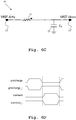
- FIG. 3A shows a MDAC that operates in two phases ⁇ S ( ⁇ Se ) and ⁇ A , which are further illustrated along Fig. 3C .
- the input V IN is sampled in the first phase ⁇ S , where it is to be noted that ⁇ Se ensures reliable early sampling.
- ⁇ Se ensures reliable early sampling.
- the difference between the reference REF and the sampled input V IN is amplified. It can be realized from Fig. 3C that the amplifier output changes fast initially during ⁇ A (time frame indicated by t slew ) . Output of the amplifier settles afterwards during some time indicated by t settle .
- Fig. 3B shows an arrangement of reference by which these orthogonal properties can be exploited. This is achieved by separating the reference REF in REF_dirty and REF_clean (that on average provide the same voltage).
- REF_dirty needs to be fast (i.e., large bandwidth specification) and does not require precision.
- the regulation of REF_clean needs to be accurate but does not require large bandwidth (i.e., high speed specification).
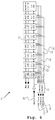
- Fig. 4 a detailed view of the device 10 according to the first aspect of the invention is illustrated.
- the regulator circuit 11 is implemented as a reference regulator and the receiving circuit 13 is implemented as a pipelined ADC.
- the pipelined ADC has multiple stages that typically contain a sub-ADC and a multiplying digital to analog converter (MDAC), followed by a staged backend.
- MDAC multiplying digital to analog converter
- the ADC inputs INp,INm are connected to the first stage STG1, that is cascaded to the second stage STG2, that is cascaded to the third stage STG3, that is further cascaded to the fourth stage STG4, that is further cascaded to the fifth stage STG5, that is further cascaded to the sixth stage STG6, that is moreover cascaded to the seventh stage STG7, and eventually terminated at the backend.
- the number of stages is not limited by this example and is basically arbitrary in most cases.
- Each stage STG1-STG7 of the pipelined ADC is realized by a sub-ADC and a MDAC circuit, for example, a 1.5b-flip-around MDAC circuit.
- Each MDAC circuit (from every stage STG1-STG7) can be individually treated as the receiving circuit 13 as well as the whole ADC where the MDAC circuits are operating collectively.
- the receiving circuit 13 is further implemented in such a way that it has fully dynamic power consumption with constant energy per conversion independent of the master clock 18 rate.
- the regulator circuit 11 is adapted to receive multiple reference inputs 12,14,16, and thereby generates regulated replicas of all or some of the reference inputs 12,14,16. It is particularly advantageous since the receiving circuit 13, herein implemented as a pipelined ADC, requires three references: two complementary references VREFP, VREFM and a common-mode reference VCM. However, only the references VREFP and VREFM are needed to be regulated with regard to high accuracy requirements, and hence the regulator circuit 11 generates two regulated replicas (12',12'' resp. 16',16") for each of the references 12,16. Whereas, the reference VCM has fixed accuracy requirements, and therefore a single regulated voltage 14' is generated by the regulator circuit 11 with regard to the said reference 14.
- the regulated replicas 12',12" resp. 16',16" are respectively defined as dirty reference and clean reference, which regard to their performance specification, e.g., low accuracy and high accuracy correspondingly.
- Fig. 5 a simplified view of a regulator block 20 according to the first aspect of the invention is illustrated.
- the receiving circuit 13 is implemented with dynamic power consumption through constant energy per conversion independent of the master clock 18 rate.
- the regulator circuit 11 is also implemented in a way such that it too is fully dynamic. This is achieved by implementing the regulator sub-blocks out of discrete-time systems as illustrated along Fig. 5 in a generalized manner.
- the regulator sub-block 20 comprises a clocked comparator 21, a charge source/sink circuitry 23 and a charge reservoir 25.
- the regulated output voltage 12' is monitored by the clocked comparator 21, which compares it to the input reference voltage 12 periodically. In the case of the pipelined ADC of Fig. 3 , the periodic comparison is performed once every full conversion of the ADC.
- the regulator sub-block 20 preferably performs passive charge sharing operation between the charge reservoir 25 and the charge source/sink circuitry 23. Depending on the output 22 of the comparator 21, charge is either added or subtracted from the charge reservoir 25 in a way that minimizes the difference between the external reference voltage 12 and the regulated output voltage 12'.
- the achievable accuracy of the regulated output 12' is a function of the size of the charge reservoir 25, the amount of charge that the source/sink circuit 23 adds or subtracts from the reservoir 25 per update 24, the amount of charge (i.e., current) pulled from the regulated output 12' by the receiving circuit 13, or a combination thereof.
- Fig. 6A, Fig. 6B , Fig. 6C and Fig. 6D different embodiments for the regulator sub-block 20 along with the timing operation are illustrated.
- the different regulator sub-blocks illustrated herein can be based on any topology or performance specification. They can formulate regulator circuits with continuous time regulation and static power consumption, or discrete time regulator circuits with dynamic power consumption and energy dissipation that scales linearly with the clock frequency, or even some hybrid or combination of both.
- a first exemplary embodiment of the regulator sub-block 30 is shown in the form of a unidirectional regulator block.
- the sizing of the charge capacitor Cp of the source/sink circuit 33 allows for passive charge sharing operation between the charge reservoir 25 and the charge source/sink circuitry 33.
- the charge capacitor Cp adds or subtracts excessive charge from the charge reservoir 25 based on the comparator's output 22, where the charging/discharging phases are controlled via a pair of PMOS switch.
- the switches are respectively controlled by a signal precharge_i and further by a signal ( connect_i+D SIGN ), where D SIGN represents the output 22 of the comparator 21, and + stands for digital OR function.
- the amount of charge per update 24 that is either added or subtracted from the charge reservoir 25 results in the accuracy of the regulated output voltage 12'.
- the regulated output voltage 12' is considered as the dirty references of the reference input signal 12 as illustrated in Fig. 4 above.
- a second exemplary embodiment of the regulator sub-block 40 is shown in the form of a bi-directional regulator block.
- the passive charging operation between the charge reservoir 25 and the charge source/sink circuitry 43 corresponds to the ratio of the charge capacitors C P ,C N and C R .
- the charging/discharging phases for each of the (dis)charge capacitors C P ,C N are respectively controlled via a pair of PMOS switches and a pair of NMOS switches.
- the PMOS switches are respectively controlled by a signal precharge_i and further by a signal ( connect_i+D SIGN ) , where D SIGN represents the output 22 of the comparator 21.
- the NMOS switches are respectively controlled by a signal precharge and further by a signal ( connect *D SIGN ), where the D SIGN represents the output 22 of the comparator 21, and * stands for digital AND function.
- the regulated output voltage 12" is considered as the clean references of the reference input signal 12 as illustrated in Fig. 4 above. This is obtained by sizing the capacitors C P and C N small with respect to C R , such that only small updates are made on the voltage on the charge reservoir. As a consequence, the regulator sub-block can only provide small charges to the receiving circuits, or can only vary its output slowly, such that this clean output voltage is highly accurate but has low bandwidth.
- the charge source/sink circuit 43 is implemented as a passive charge-sharing operation between the charge reservoir 25 and the capacitors C P /C N , there are other possible methods for generating the charge transfer.
- one alternative is to use a charge-pump configuration for C P /C N , which would allow for a significantly larger amount of charge to be added or subtracted to the charge reservoir 25 for a given sizing of C P /C N .
- a third exemplary embodiment of the regulator sub-block 50 is shown in the form of a fully passive regulator block. Due to the absence of any comparator as utilized in sub-blocks 30 and 40, the functionality of the regulator sub-block 50 is used in a way that it takes charge from one already regulated replica's output 12', for instance, from the dirty references, and delivers further regulated output 12" in the form of clean references by means of low pass filtration. In other words, the regulator sub-block 50 generates a regulated replica 12" of the input reference signal 12 with respect to any of the already generated replicas 12' instead of generating the output independently.
- the regulator sub-block 50 comprises a resistor 51 that defines the charging and/or discharging phases of the charge reservoir 25.
- This resistor 51 can be a variable resistor to trade off the bandwidth and the accuracy of the regulated output 12".
- This resistor 51 can be implemented as a switched capacitor resistor, which has an equivalent resistance value inversely proportional to its capacitor value and its clock frequency.
- Fig. 6D a simplified timing diagram for the clock operation in the regulator blocks 30 and 40 is illustrated. Especially, the nature for clocks regarding the signals precharge, precharge_i , connect and connect_i are shown here with their mutual timing arrangements.
- Fig. 7A and 7B different embodiments for the regulator circuit 11 are illustrated in blocks by way of the top level reference regulator shown in Fig. 4 above.
- Fig. 7A shows a first exemplary embodiment of the regulator circuit 60 where multiple input reference signals are inputted. However, not every input reference signals are required to be replicated into two regulated output signals.
- the pipelined ADC requires three references: VREFP, VREFM and VCM, where only the VREFP and VREFM are needed to be regulated with regard to high accuracy requirements, since VCM has reduced accuracy requirements.
- the regulator circuit 60 comprises a parallel arrangement of the regulator sub-blocks 30 and 40, where the regulator sub-block 30 outputs the dirty reference 12' replicated from the reference input 12 and the regulator sub-block 40 outputs the clean references 12" replicated from the reference input 12.
- the regulator sub-block 30 generates the dirty references VREFP_dirty and the regulator sub-block 40 generates the clean references VREFP_clean. This is analogously performed for the VREFM reference.
- the top-level reference regulator 60 illustrated herein is able to handle multiple input reference signals 12,13,14, preferably multiple simultaneous reference inputs and generates regulated replicas independently as per the requirement of the receiving circuit 13, e.g., accuracy. It is also explicit that the number of input reference signals can be extended and can be effectively handled by the regulator circuit 11 by incorporating additional respective regulator sub-blocks 30,40.
- a second exemplary embodiment of the regulator circuit 70 is shown by way of the top-level reference regulator.
- the regulator circuit 70 differs from the regulator circuit 60 of Fig. 7A in that the regulator circuit 70 comprises the regulator sub-block 50 instead of the regulator sub-block 40 particularly for generating regulated replicas of the reference signal.
- the regulator sub-block 30 is used for the dirty references and the regulator sub-block 50 is used for the clean references.
- This arrangement of the regulator sub-blocks 30 and 50 is limited to the operations where the frequency content of the current pulled from the dirty regulated output is primarily at relatively higher frequencies. This means that the error of that output is also high-frequency in nature. By low pass filtering it via the regulator sub-block 50, this error can be removed, and can be provided as a second replica output (i.e., the clean references) that will have higher accuracy and lower error.
- the amount of low pass filtering possible is further limited by the amount of DC current that must be provided to the receiving circuit 13 by the clean reference.
- the current drawn from the clean reference by the receiving circuit 13 is significantly less than the current drawn from the dirty reference by the receiving circuit 13, and so this arrangement can be effectively utilized for the regulator circuit 11. If, however, this is not the case, then an active regulation may be necessary for the clean references as implemented in the regulator circuit 60 of Fig. 7A .
- a first exemplary embodiment for the receiving circuit 80 is illustrated.
- the implemented receiving circuit 80 corresponds to the 1.5b-flip-around MDAC circuit implemented as a part of each stage of the pipelined ADC as shown in Fig. 4 .
- the receiving circuit 80 is a discrete-time switched-capacitor signal processing circuit, which covers a broad scope of circuit and applications.
- the receiving circuit 80 is realized in the context of a MDAC circuit, preferably used but not limited to pipelined ADCs.
- the receiving circuit 80 is preferred to be implemented in cascade along with the preceding and following stages through the input signal line 81 and output signal line 82.
- the receiving circuit 80 comprises switched-capacitor arrangement 84 followed by a residue amplifier 83 in order to settle the output to a certain solution.
- the receiving circuit 80 further comprises switching means 85 that allows the receiving circuit 80 to switch from one regulated replica 12' to another regulated replica 12".
- the conventional MDAC circuit has been modified to be able to switch between the multiple regulated replicas 12',12'.
- the switching criteria is defined via a slew-done signal 86 generated by a detector means (not shown).
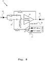
- Fig. 9 a detailed view of the receiving circuit 80 is illustrated, especially for the specific case of the 1.5b-flip-around MDAC. It has the capability to switch from the dirty references 12' resp. 16' to the clean references 12" resp. 16'' when the slew-done input signal 86 asserts. In is further comprehensible that the switching is done in a non-overlapping manner so that no charge can transfer directly from one reference to the other. Preferably, dummy switches are also included at the outputs in order to cancel charge injection and clock feedthrough, which minimizes the size of the glitch that happens in the MDAC when the switch-over occurs.
- FIG. 10A shows an example implementation of the slew-done detector 87.
- the implementation illustrated herein is based on the MDAC circuit of Fig. 8 and Fig. 9 , where a ring amplifier is used as the residue amplifier 83. It operates based on the principle that only after slewing has finished will the binary quantized logic equation AB'CD' evaluate to "1".
- Fig. 10B the transient waveform operation of this principle is shown.
- This slew-done signal 86 can then be fed to the receiving circuit 80, i.e., the MDAC circuit, to initiate the switching from dirty to clean reference.
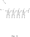
- a second exemplary embodiment for the receiving circuit 90 is illustrated.
- the receiving circuit 90 has been implemented by means of a switched-capacitor charge-redistribution DAC, as is very commonly used in SAR ADCs.
- the receiving circuit 90 resembles a top-plate-sampled 4bit DAC with cascaded four weighted stages 91,93,95,97 and further a reference node 99.
- the minimum set of voltage inputs i.e., the dirty reference and ground
- One possible consideration can be based on the assumption that the DAC 90 is used in a feedback loop with a comparator to operate as a SAR ADC. Further assumption can be made that some amount of redundancy is built into the SAR algorithm, either by extra comparison steps or any other method of redundancy. Due to the redundancy, the overall accuracy of the reference when resolving the MSBs 97 is significantly less than the accuracy required when resolving the final LSBs 91.
- the MSBs 97 can be switched using the REF dirty connection, and at the LSBs 91 all capacitors connected to REF dirty can be switched over to REF clean instead, and the final LSBs 91 can be resolved using the high accuracy reference.
- the limit-case of the said example can be considered, where the majority (or entire, even) conversion is performed using the dirty reference, and only at the final search step (or after, even) are the capacitors connected to REF dirty switched over to REF clean instead.
- This way only a very small error charge must be sourced by the clean reference, relaxing its regulator's design ever further.
- this alternative does not allow for correction of errors based on redundancy, in many applications it may still be useful.
- the error-correction redundancy is often built into the inter-stage gain.
- the first stage SAR ADC's conversion accuracy requirement is much less than the accuracy requirement for it's residue that will be passed on to the next stage.
- the SAR itself only needs to be 5b accurate, but the 5b DAC's residue must be at least 10b accurate.
- the described operation scheme can be very useful. The vast majority of the charge still comes from the dirty reference, but the full accuracy of the clean reference determines the final DAC residue accuracy.
- a first step 100 two or more replicas of the reference signal are generated as regulated output signals.
- a second step 101 the regulated output signals are received in a switchable manner, wherein the regulated output signals are defined with different performance specifications.
- the embodiments of the present invention can be implemented by hardware, software, or any combination thereof.
- Various embodiments of the present invention may be implemented by one or more application specific integrated circuits (ASICs), digital signal processors (DSPs), digital signal processing devices (DSPDs), programmable logic devices (PLDs), field programmable gate arrays (FPGAs), processors, controllers, microcontrollers, microprocessors, or the like.
- ASICs application specific integrated circuits
- DSPs digital signal processors
- DSPDs digital signal processing devices
- PLDs programmable logic devices
- FPGAs field programmable gate arrays
- processors controllers, microcontrollers, microprocessors, or the like.
Landscapes
- Engineering & Computer Science (AREA)
- Theoretical Computer Science (AREA)
- Power Engineering (AREA)
- Computer Hardware Design (AREA)
- Physics & Mathematics (AREA)
- Computing Systems (AREA)
- Mathematical Physics (AREA)
- General Engineering & Computer Science (AREA)
- Dc-Dc Converters (AREA)
- Electromagnetism (AREA)
- General Physics & Mathematics (AREA)
- Radar, Positioning & Navigation (AREA)
- Automation & Control Theory (AREA)
Abstract
Description
- The invention relates to replicating a reference signal, especially for enhancing the performance of voltage regulation in electronic circuits and systems through the use of multiple regulated outputs.
- Voltage regulation is a widely utilized technique in electronic circuits and systems. Generally, the power consumption of a voltage regulator depends on the particular needs of the load that it is providing charge to or absorbing charge from. Each loading circuit has its own charge or discharge profile across both frequency and time, and also has its own accuracy requirements for how close to ideal the regulated voltage must be in order to minimize the influence of error on overall circuit performance.
- In analog and mixed-signal circuits, the loading circuit is often very complex and if considered to be a black-box with no internal knowledge of operation, it is not practical to predict the instantaneous current draw of the system at any particular moment in time. The regulator must be designed such that at any moment in time it will have enough bandwidth and current sourcing capability to track changes in the load and keep the regulated voltage within required reference ripple bounds. This ultimately manifests as a tradeoff in the total power consumption and overall power efficiency of the regulator.
- For example, the document
US 6,031,362 A shows a technique for optimizing the power consumption of low drop out (LDO) linear voltage regulators by optimizing the output voltage of a switch mode power supply (SMPS). The optimization is performed by using feedback to control the output voltage of the SMPS that is used as the input voltage to subsequent LDO regulators. A multiplexer and an analog to digital converter (ADC) are used to successively sample the output voltages of multiple parallel LDO regulators. The digitized voltage values are then inputted to a digital processor that compares the LDO regulator output voltages with acceptable limits previously stored in memory. - However, the successive voltage switching for addressing the power consumption of LDO regulators by means of the integrated ADC, multiplexer and further digital processing means lead to a more complex and cost-intensive system. Moreover, the overall power efficiency of voltage regulation with respect to the load, e.g., an ADC, cannot be effectively identified either for a single LDO regulator or for the whole voltage regulation arrangement of multiple parallel LDO regulators.
- Accordingly, the object of the invention is to provide a device and a method for enhancing the performance of voltage regulation in a simple and cost-effective manner, which is further able to trade the power consumption and overall power efficiency of voltage regulation, especially with respect to the accuracy requirements of the load circuit.
- The object is solved by the features of the first independent claim for the device and by the features of the second independent claim for the method. The dependent claims contain further developments.
- According to a first aspect of the invention, a device for buffering a reference signal is provided. The device comprises a regulator circuit adapted to generate at least two replicas of the reference signal as regulated output signals. The device further comprises a receiving circuit adapted to receive the regulated output signals in a switchable manner. In this context, the regulated output signals are defined with different performance specifications.
- Therefore, the regulator circuit generates two or more replicas of the input reference signal, e.g., voltage, as regulated output voltages. The regulated output voltages are advantageously defined in terms of, for instance, accuracy, output impedance, bandwidth, etc. The receiving circuit utilizes these multiple copies so as to reduce the total power consumption of the regulator circuit. Moreover, the regulated output signals are consistent with each other, especially with respect to their average output voltages. Advantageously, effective voltage regulation can be performed, especially in terms of reference regulation.
- According to a first preferred implementation form of said first aspect of the invention, the regulator circuit comprises a plurality of regulator sub-blocks adapted to each generate a respective regulated output signal. In this context, the plurality of regulator sub-blocks are further adapted to generate the regulated output signals independently. Hence, the performance of each regulated replica can be independently defined, especially in terms of specifications of accuracy, output impedance, bandwidth, etc.
- Furthermore, the plurality of regulator sub-blocks are preferably defined with different regulator topologies and/or performance specifications. Advantageously, the performance of each regulated replica can be independently defined in terms of the particular regulator block that is used to meet the specifications of the regulated replica.
- According to a second preferred implementation form of said first aspect of the invention, each regulator sub-block comprises a clocked comparator, a charge reservoir and a charge source/sink circuitry, whereby the clocked comparator is adapted to compare the regulated output signal to the reference signal. Advantageously, the simplified implementation of each regulator block allows for a cost-effective but enhanced voltage regulation performance.
- According to a further preferred implementation form of said first aspect of the invention, the regulator sub-block is further adapted to perform charge sharing operation between the charge reservoir and the charge source/sink circuitry. In other words, charge can either be added or subtracted from the charge reservoir so as to minimize the difference between the reference input voltage or the ideal output voltage and the regulated output voltage.
- According to a further preferred implementation form of said first aspect of the invention, the regulator sub-block further comprises a variable resistor adapted to define charging and/or discharging of the charge reservoir. In addition to this or as an alternative, the variable resistor can be implemented as a switched capacitor resistor, which has an equivalent resistance value inversely proportional to its capacitor value and its clock frequency.
- According to a further preferred implementation form of said first aspect of the invention, the regulator circuit is further adapted to receive a plurality of reference signals and whereby the regulator circuit is able to generate at least two replicas of all or some of the reference signals as regulated output signals. Advantageously, flexible circuit implementation is incorporated, particularly in terms of the loading circuit implementation.
- According to a further preferred implementation form of said first aspect of the invention, the receiving circuit comprises switching means adapted to switch from one regulated output signal to another in a non-overlapping manner. Advantageously, the receiving circuit supports switching from one regulated replica to another.
- According to a further preferred implementation form of said first aspect of the invention, the receiving circuit is a discrete-time switched-capacitor signal processing circuit and whereby the regulator circuit is adapted to function as a reference regulator for the signal processing circuit. The receiving circuit can be further referred to as signal conversion circuits, for instance, an analog to digital converter (ADC) circuit. Advantageously, the regulator circuit is adapted to deliver reference voltages that are used to provide an absolute measure of voltage amplitudes in signal conversion.
- According to a further preferred implementation form of said first aspect of the invention, the receiving circuit further comprises a detector means adapted to provide control signals to the switching means in order to switch from one regulated output signal to another at an optimal time instant at which the desired performance specification of the regulated output signal changes. In this context, the detector means is further adapted to produce a slew-done signal indicating that the receiving circuit stops slewing and commences settling behavior. Advantageously, optimal or near-optimal switching instances or criteria can be defined by means of the slew-done signal when the receiving circuit should switch between the regulated replicas.
- According to a further preferred implementation form of said first aspect of the invention, the detector means is further adapted to sense a delayed version of a trigger signal at which the receiving circuit starts its operation. Advantageously, an additional yet simplified switching criterion is implemented.
- According to a further preferred implementation form of said first aspect of the invention, one of the at least two replicas of the reference signal is defined with high speed but low accuracy specification thereby generating a first regulated output signal and the other is defined with low speed but high accuracy specification thereby generating a second regulated output signal. In this context, the receiving circuit is adapted to utilize the first regulated output signal and the second regulated output signal successively. Advantageously, the device allows for a tradeoff between the overall power efficiency of voltage regulation and the accuracy requirements of the load circuit.
- According to a second aspect of the invention, a method for buffering a reference signal is provided. The method comprises the steps of generating at least two replicas of the reference signal as regulated output signals and receiving the regulated output signals in a switchable manner. In this context, the regulated output signals are defined with different performance specifications. Advantageously, the total power consumption for voltage regulation is effectively reduced in a simplified manner.
- According to a first preferred implementation form of said second aspect of the invention, the method further comprises the step of generating the regulated output signals independently. Advantageously, the performance of each regulated replica can be independently defined, especially in terms of specifications of accuracy, output impedance, bandwidth, etc.
- According to a second preferred implementation form of said second aspect of the invention, the method further comprises the step of receiving a plurality of reference signals and whereby generating two or more replicas of all or some of the reference signals as regulated output signals. Advantageously, flexible circuit implementation is incorporated, particularly in terms of the loading circuit implementation.
- Exemplary embodiments of the invention are now further explained with respect to the drawings by way of example only, and not for limitation. In the drawings:
- Fig. 1
- shows a generalized voltage regulation scheme;
- Fig. 2
- shows an exemplary embodiment of the device according to the first aspect of the invention;
- Fig. 3A
- shows an example MDAC operating in two phases;
- Fig. 3B
- shows an exemplary reference arrangement for the MDAC;
- Fig. 3C
- shows the timing operation of the MDAC by way of an example;
- Fig. 4
- shows a detailed view of the device according to the first aspect of the invention;
- Fig. 5
- shows a simplified view of a regulator block according to the first aspect of the invention;
- Fig. 6A
- shows a first exemplary embodiment of the regulator block;
- Fig. 6B
- shows a second exemplary embodiment of the regulator block;
- Fig. 6C
- shows a third exemplary embodiment of the regulator block;
- Fig. 6D
- shows a simplified timing diagram for the clock operation in the regulator blocks of
Fig. 5A-5C ; - Fig. 7A
- shows a first exemplary embodiment of the regulator circuit in blocks;
- Fig. 7B
- shows a second exemplary embodiment of the regulator circuit in blocks;
- Fig. 8
- shows a first exemplary embodiment for the receiving circuit implementation;
- Fig. 9
- shows a detailed view of the receiving circuit of
Fig. 7 ; - Fig. 10A
- shows an exemplary embodiment for the detector means implementation;
- Fig. 10B
- shows a graphical illustration representing the operation of the circuit of
Fig. 9 by way of an example; - Fig. 11
- shows a second exemplary embodiment for the receiving circuit implementation; and
- Fig. 12
- shows an exemplary embodiment of the method according to the second aspect of the invention.
- Reference will now be made in detail to the embodiments of the present invention, examples of which are illustrated in the accompanying drawings. However, the following embodiments of the present invention may be variously modified and the range of the present invention is not limited by the following embodiments.
- In
Fig. 1 , a generalized voltage regulation scheme is shown. Especially, the basic purpose of avoltage regulator 1 is illustrated herein. Theregulator 1 takes a reference voltage 2 of any impedance as an input (e.g., VREF) and buffers this voltage to the output (e.g., VREG) as a regulated voltage 2', with an output impedance that has been adjusted to meet the needs of the receiving circuits further downstream. Typically, the regulated output voltage 2' is desired to have a low output impedance across a wide bandwidth, so that theregulator 1 can source current to the connected circuits that pull charge from VREG while still maintaining a stable and accurate matching of the voltages VREF and VREG. Any deviation from this equality results in an inaccurate reproduction of VREF and constitutes a source of error, for instance, reference noise, reference ripple, reference error and the like, for the connected circuits. An ideal regulator is therefore a voltage source with zero output impedance across infinite bandwidth. - The purpose of said voltage regulation scheme is very broad, and encompasses both supply regulation and reference regulation. Supply regulation generally refers to the case where VREG serves as a power supply for analog and/or digital circuits. Reference regulation generally refers to the case where VREG serves as a reference voltage that is used to provide an absolute measure of voltage amplitude in an analog and/or mixed-signal circuit. For example, a voltage reference is used in an analog to digital (ADC) or digital to analog (DAC) circuit to define the full-scale voltage range against which all sampled input (for ADC) or output (for DAC) voltages are quantized with respect to.
- In
Fig. 2 , an exemplary embodiment of thedevice 10 according to the first aspect of the invention is illustrated. In particular, a simplified form of the proposed solution is illustrated herein in a block diagram. Thedevice 10 comprises aregulator circuit 11 that generates two replicas of aninput reference signal 12 or reference voltage (e.g., VREF) asregulated output voltages 12',12" (e.g., VREG1, VREG2). Thedevice 10 further comprises a receivingcircuit 13 that receives theregulated replicas 12', 12" in a switchable manner. Theregulated replicas 12', 12" are defined with different performance specifications in terms of accuracy, output impedance, bandwidth and so on, and therefore the receivingcircuit 13 can utilize thesereplicas 12',12" in order to reduce the performance requirements for theregulator circuit 11. - In addition, the performance of each regulated replica 12',12'' can be independently defined in terms of specifications of accuracy, output impedance, bandwidth, etc. For instance, one regulated replica 12' may correspond to the regulated replica of the
reference voltage 12 with low accuracy. While the otherregulated replica 12" may correspond to the regulated replica of thereference voltage 12 with high accuracy. Although only tworegulated replicas 12', 12" are illustrated herein, it is possible to generate more than two regulated replicas of thereference voltage 12 if needed by the receivingcircuit 13. - Furthermore, the performance of each regulated replica 12',12'' can be independently defined in terms of the particular regulator circuit that is used to meet these specifications. For example, there are power efficient regulator topologies that can provide a large bandwidth but suffer from low accuracy. On the other hand, it is also possible to build an efficient regulator that can provide high accuracy, but which suffers from low bandwidth. In order to build a regulator that is both high accuracy and high bandwidth, the power efficiency will be significantly worse than either of the two aforementioned cases.
- With the feasibility of generating two
regulated replicas 12', 12" of thereference voltage 12, theregulator circuit 11 allows to decouple these two opposing design constrains (e.g., accuracy or bandwidth) and utilizes two or more high-efficiency regulator topologies, each optimized differently for a certain level of performance with respect to accuracy, bandwidth, peak current delivery, etc. - Moreover, it is known in the art that many forms of the receiving
circuit 13, e.g. signal conversion circuits, operate with a high degree of orthogonality with respect to accuracy and bandwidth (i.e., output impedance). In other words, many practical signal processing circuits only require either accuracy or low output impedance (i.e., bandwidth) from the regulated reference or supply at any particular instant of time, but not both at the same time. This happens if the circuit does not need high accuracy when it is pulling relatively large amounts of current from the reference or supply and rather only needs high accuracy at moments in time when it is pulling relatively small amounts of current from the reference or supply. This is often the case in any system that uses residue amplifiers to settle to a solution, such as in a multiplying digital to analog converter (MDAC) of a pipelined analog to digital converter (ADC). This is also often the case in any system that uses charge-redistribution DACs to perform an iterative search, such as in a successive approximation (SAR) ADC. - An example of such a switched-capacitor circuit is shown along
Fig. 3A, Fig. 3B and Fig. 3C in context of a MDAC.Fig. 3A shows a MDAC that operates in two phases φS (φ Se ) and φA , which are further illustrated alongFig. 3C . The input VIN is sampled in the first phase φS , where it is to be noted that φSe ensures reliable early sampling. In the second phase φA , the difference between the reference REF and the sampled input VIN is amplified. It can be realized fromFig. 3C that the amplifier output changes fast initially during φ A (time frame indicated by tslew ). Output of the amplifier settles afterwards during some time indicated by tsettle. - It is further important to note that in such an arrangement, a substantial initial charge can be pulled fast from the reference REF during tslew. The amplifier changes its output significantly in this time frame. During settling tsettle , less charge is pulled from the reference since the output of the amplifier mostly stabilizes around a final potential. At the end of the amplification phase, the following stage (not shown) samples the amplifier output. A precise sample is often required. The two distinct phases of amplification impose significantly different requirements on the reference REF. Initially at or during tslew , it is necessary to pull charge fast, where precision is less of a concern. Throughout tsettle , there is little charge pull from the reference REF, but the voltage needs to be accurate (for precise sampling in the following stage).
-
Fig. 3B shows an arrangement of reference by which these orthogonal properties can be exploited. This is achieved by separating the reference REF in REF_dirty and REF_clean (that on average provide the same voltage). The regulation for REF_dirty, however, needs to be fast (i.e., large bandwidth specification) and does not require precision. The regulation of REF_clean needs to be accurate but does not require large bandwidth (i.e., high speed specification). - In
Fig. 4 , a detailed view of thedevice 10 according to the first aspect of the invention is illustrated. Theregulator circuit 11 is implemented as a reference regulator and the receivingcircuit 13 is implemented as a pipelined ADC. The pipelined ADC has multiple stages that typically contain a sub-ADC and a multiplying digital to analog converter (MDAC), followed by a staged backend. The ADC inputs INp,INm are connected to the first stage STG1, that is cascaded to the second stage STG2, that is cascaded to the third stage STG3, that is further cascaded to the fourth stage STG4, that is further cascaded to the fifth stage STG5, that is further cascaded to the sixth stage STG6, that is moreover cascaded to the seventh stage STG7, and eventually terminated at the backend. Although a total of seven stages are illustrated herein, it is to be understood that the number of stages is not limited by this example and is basically arbitrary in most cases. - Each stage STG1-STG7 of the pipelined ADC is realized by a sub-ADC and a MDAC circuit, for example, a 1.5b-flip-around MDAC circuit. Each MDAC circuit (from every stage STG1-STG7) can be individually treated as the receiving
circuit 13 as well as the whole ADC where the MDAC circuits are operating collectively. The receivingcircuit 13 is further implemented in such a way that it has fully dynamic power consumption with constant energy per conversion independent of themaster clock 18 rate. - The
regulator circuit 11 is adapted to receivemultiple reference inputs reference inputs circuit 13, herein implemented as a pipelined ADC, requires three references: two complementary references VREFP, VREFM and a common-mode reference VCM. However, only the references VREFP and VREFM are needed to be regulated with regard to high accuracy requirements, and hence theregulator circuit 11 generates two regulated replicas (12',12'' resp. 16',16") for each of thereferences regulator circuit 11 with regard to the saidreference 14. Theregulated replicas 12',12" resp. 16',16" are respectively defined as dirty reference and clean reference, which regard to their performance specification, e.g., low accuracy and high accuracy correspondingly. - In
Fig. 5 , a simplified view of aregulator block 20 according to the first aspect of the invention is illustrated. As already mentioned above, the receivingcircuit 13 is implemented with dynamic power consumption through constant energy per conversion independent of themaster clock 18 rate. In order to preserve this highly advantageous property for the full chip-level system, theregulator circuit 11 is also implemented in a way such that it too is fully dynamic. This is achieved by implementing the regulator sub-blocks out of discrete-time systems as illustrated alongFig. 5 in a generalized manner. - The
regulator sub-block 20 comprises a clockedcomparator 21, a charge source/sink circuitry 23 and acharge reservoir 25. The regulated output voltage 12' is monitored by the clockedcomparator 21, which compares it to theinput reference voltage 12 periodically. In the case of the pipelined ADC ofFig. 3 , the periodic comparison is performed once every full conversion of the ADC. Theregulator sub-block 20 preferably performs passive charge sharing operation between thecharge reservoir 25 and the charge source/sink circuitry 23. Depending on theoutput 22 of thecomparator 21, charge is either added or subtracted from thecharge reservoir 25 in a way that minimizes the difference between theexternal reference voltage 12 and the regulated output voltage 12'. - Normally, the achievable accuracy of the regulated output 12' is a function of the size of the
charge reservoir 25, the amount of charge that the source/sink circuit 23 adds or subtracts from thereservoir 25 perupdate 24, the amount of charge (i.e., current) pulled from the regulated output 12' by the receivingcircuit 13, or a combination thereof. - Along
Fig. 6A, Fig. 6B ,Fig. 6C and Fig. 6D , different embodiments for theregulator sub-block 20 along with the timing operation are illustrated. In the broadest sense, the different regulator sub-blocks illustrated herein can be based on any topology or performance specification. They can formulate regulator circuits with continuous time regulation and static power consumption, or discrete time regulator circuits with dynamic power consumption and energy dissipation that scales linearly with the clock frequency, or even some hybrid or combination of both. - In
Fig. 6A , a first exemplary embodiment of theregulator sub-block 30 is shown in the form of a unidirectional regulator block. The sizing of the charge capacitor Cp of the source/sink circuit 33 allows for passive charge sharing operation between thecharge reservoir 25 and the charge source/sink circuitry 33. The charge capacitor Cp adds or subtracts excessive charge from thecharge reservoir 25 based on the comparator'soutput 22, where the charging/discharging phases are controlled via a pair of PMOS switch. The switches are respectively controlled by a signal precharge_i and further by a signal (connect_i+DSIGN ), where DSIGN represents theoutput 22 of thecomparator 21, and + stands for digital OR function. The amount of charge perupdate 24 that is either added or subtracted from thecharge reservoir 25 results in the accuracy of the regulated output voltage 12'. Herein, the regulated output voltage 12' is considered as the dirty references of thereference input signal 12 as illustrated inFig. 4 above. - In
Fig. 6B , a second exemplary embodiment of theregulator sub-block 40 is shown in the form of a bi-directional regulator block. Here, the passive charging operation between thecharge reservoir 25 and the charge source/sink circuitry 43 corresponds to the ratio of the charge capacitors CP,CN and CR. The charging/discharging phases for each of the (dis)charge capacitors CP,CN are respectively controlled via a pair of PMOS switches and a pair of NMOS switches. The PMOS switches are respectively controlled by a signal precharge_i and further by a signal (connect_i+DSIGN ), where DSIGN represents theoutput 22 of thecomparator 21. Similarly, the NMOS switches are respectively controlled by a signal precharge and further by a signal (connect *DSIGN ), where the DSIGN represents theoutput 22 of thecomparator 21, and * stands for digital AND function. - Herein, the
regulated output voltage 12" is considered as the clean references of thereference input signal 12 as illustrated inFig. 4 above. This is obtained by sizing the capacitors CP and CN small with respect to CR, such that only small updates are made on the voltage on the charge reservoir. As a consequence, the regulator sub-block can only provide small charges to the receiving circuits, or can only vary its output slowly, such that this clean output voltage is highly accurate but has low bandwidth. - It is to be noted that, although in the above-mentioned implementation the charge source/
sink circuit 43 is implemented as a passive charge-sharing operation between thecharge reservoir 25 and the capacitors CP/CN, there are other possible methods for generating the charge transfer. For example, one alternative is to use a charge-pump configuration for CP/CN, which would allow for a significantly larger amount of charge to be added or subtracted to thecharge reservoir 25 for a given sizing of CP/CN. - In
Fig. 6C , a third exemplary embodiment of theregulator sub-block 50 is shown in the form of a fully passive regulator block. Due to the absence of any comparator as utilized insub-blocks regulator sub-block 50 is used in a way that it takes charge from one already regulated replica's output 12', for instance, from the dirty references, and delivers further regulatedoutput 12" in the form of clean references by means of low pass filtration. In other words, theregulator sub-block 50 generates aregulated replica 12" of theinput reference signal 12 with respect to any of the already generated replicas 12' instead of generating the output independently. - In order to perform low pass filtration, the
regulator sub-block 50 comprises aresistor 51 that defines the charging and/or discharging phases of thecharge reservoir 25. Thisresistor 51 can be a variable resistor to trade off the bandwidth and the accuracy of theregulated output 12". Thisresistor 51 can be implemented as a switched capacitor resistor, which has an equivalent resistance value inversely proportional to its capacitor value and its clock frequency. - In
Fig. 6D , a simplified timing diagram for the clock operation in the regulator blocks 30 and 40 is illustrated. Especially, the nature for clocks regarding the signals precharge, precharge_i, connect and connect_i are shown here with their mutual timing arrangements. - Along
Fig. 7A and7B , different embodiments for theregulator circuit 11 are illustrated in blocks by way of the top level reference regulator shown inFig. 4 above. In particular,Fig. 7A shows a first exemplary embodiment of theregulator circuit 60 where multiple input reference signals are inputted. However, not every input reference signals are required to be replicated into two regulated output signals. As described alongFig. 4 , the pipelined ADC requires three references: VREFP, VREFM and VCM, where only the VREFP and VREFM are needed to be regulated with regard to high accuracy requirements, since VCM has reduced accuracy requirements. - Here, the
regulator circuit 60 comprises a parallel arrangement of theregulator sub-blocks regulator sub-block 30 outputs the dirty reference 12' replicated from thereference input 12 and theregulator sub-block 40 outputs theclean references 12" replicated from thereference input 12. For instance, as the reference VREFP is needed to be regulated with high accuracy, theregulator sub-block 30 generates the dirty references VREFP_dirty and theregulator sub-block 40 generates the clean references VREFP_clean. This is analogously performed for the VREFM reference. - However, since the VCM reference has reduced accuracy requirements, only the
regulator sub-block 40 is utilized in order to generate only the clean reference for the receivingcircuit 13. As a result, the top-level reference regulator 60 illustrated herein is able to handle multiple input reference signals 12,13,14, preferably multiple simultaneous reference inputs and generates regulated replicas independently as per the requirement of the receivingcircuit 13, e.g., accuracy. It is also explicit that the number of input reference signals can be extended and can be effectively handled by theregulator circuit 11 by incorporating additionalrespective regulator sub-blocks - In
Fig. 7B , a second exemplary embodiment of theregulator circuit 70 is shown by way of the top-level reference regulator. Theregulator circuit 70 differs from theregulator circuit 60 ofFig. 7A in that theregulator circuit 70 comprises theregulator sub-block 50 instead of theregulator sub-block 40 particularly for generating regulated replicas of the reference signal. Thus, for the references VREFP resp. VREFM, theregulator sub-block 30 is used for the dirty references and theregulator sub-block 50 is used for the clean references. - This arrangement of the
regulator sub-blocks regulator sub-block 50, this error can be removed, and can be provided as a second replica output (i.e., the clean references) that will have higher accuracy and lower error. - Moreover, the amount of low pass filtering possible (i.e., error suppression) is further limited by the amount of DC current that must be provided to the receiving
circuit 13 by the clean reference. As mentioned before, it is often the case that the current drawn from the clean reference by the receivingcircuit 13 is significantly less than the current drawn from the dirty reference by the receivingcircuit 13, and so this arrangement can be effectively utilized for theregulator circuit 11. If, however, this is not the case, then an active regulation may be necessary for the clean references as implemented in theregulator circuit 60 ofFig. 7A . - In
Fig. 8 , a first exemplary embodiment for the receivingcircuit 80 is illustrated. In particular, the implemented receivingcircuit 80 corresponds to the 1.5b-flip-around MDAC circuit implemented as a part of each stage of the pipelined ADC as shown inFig. 4 . However, in the broadest sense, there is no restriction to what the receivingcircuit 80 can be. In the most direct applications, the receivingcircuit 80 is a discrete-time switched-capacitor signal processing circuit, which covers a broad scope of circuit and applications. As an exemplary embodiment illustrated herein, the receivingcircuit 80 is realized in the context of a MDAC circuit, preferably used but not limited to pipelined ADCs. - The receiving
circuit 80 is preferred to be implemented in cascade along with the preceding and following stages through theinput signal line 81 andoutput signal line 82. The receivingcircuit 80 comprises switched-capacitor arrangement 84 followed by aresidue amplifier 83 in order to settle the output to a certain solution. The receivingcircuit 80 further comprises switching means 85 that allows the receivingcircuit 80 to switch from one regulated replica 12' to anotherregulated replica 12". Hence, the conventional MDAC circuit has been modified to be able to switch between the multiple regulated replicas 12',12'. The switching criteria is defined via a slew-donesignal 86 generated by a detector means (not shown). - In
Fig. 9 , a detailed view of the receivingcircuit 80 is illustrated, especially for the specific case of the 1.5b-flip-around MDAC. It has the capability to switch from the dirty references 12' resp. 16' to theclean references 12" resp. 16'' when the slew-doneinput signal 86 asserts. In is further comprehensible that the switching is done in a non-overlapping manner so that no charge can transfer directly from one reference to the other. Preferably, dummy switches are also included at the outputs in order to cancel charge injection and clock feedthrough, which minimizes the size of the glitch that happens in the MDAC when the switch-over occurs. - Along
Fig. 10A andFig. 10B , the implementation and operation of a detector means or a so-called slew-donedetector 87 are illustrated. In particular,Fig. 10A shows an example implementation of the slew-donedetector 87. The implementation illustrated herein is based on the MDAC circuit ofFig. 8 andFig. 9 , where a ring amplifier is used as theresidue amplifier 83. It operates based on the principle that only after slewing has finished will the binary quantized logic equation AB'CD' evaluate to "1". InFig. 10B , the transient waveform operation of this principle is shown. This slew-donesignal 86 can then be fed to the receivingcircuit 80, i.e., the MDAC circuit, to initiate the switching from dirty to clean reference. - Since the vast majority of charge pulled from the references occurs during slewing, as shown in
Fig. 10B , switching at this moment ensures that only a small fraction of the total charge pull will be taken from the high-accuracyclean reference 12",14". Meanwhile, the accuracy of the reference when slewing does not need to be high, but the accuracy of the reference after slewing (i.e., settling) does need to be high. This orthogonal operation further supports that it is often the case that when a circuit needs low output impedance from the reference, it does not need high accuracy, and that when it needs high accuracy, it does not need low output impedance. - In
Fig. 11 , a second exemplary embodiment for the receiving circuit 90 is illustrated. In particular, the receiving circuit 90 has been implemented by means of a switched-capacitor charge-redistribution DAC, as is very commonly used in SAR ADCs. The receiving circuit 90 resembles a top-plate-sampled 4bit DAC with cascaded fourweighted stages - One possible consideration can be based on the assumption that the DAC 90 is used in a feedback loop with a comparator to operate as a SAR ADC. Further assumption can be made that some amount of redundancy is built into the SAR algorithm, either by extra comparison steps or any other method of redundancy. Due to the redundancy, the overall accuracy of the reference when resolving the
MSBs 97 is significantly less than the accuracy required when resolving thefinal LSBs 91. - Meanwhile, the vast majority of charge will be taken from the reference by the
MSBs 97, while only a small remainder will be pulled by theLSBs 91. Thus, it can be seen that orthogonality of accuracy of the reference versus required output impedance of the reference can be achieved in the receiving circuit 90. Therefore, theMSBs 97 can be switched using the REF dirty connection, and at theLSBs 91 all capacitors connected to REF dirty can be switched over to REF clean instead, and thefinal LSBs 91 can be resolved using the high accuracy reference. - As an alternative to the foregoing example, the limit-case of the said example can be considered, where the majority (or entire, even) conversion is performed using the dirty reference, and only at the final search step (or after, even) are the capacitors connected to REF dirty switched over to REF clean instead. This way, only a very small error charge must be sourced by the clean reference, relaxing its regulator's design ever further. Although this alternative does not allow for correction of errors based on redundancy, in many applications it may still be useful.
- For example, in the case of a pipelined-SAR ADC, the error-correction redundancy is often built into the inter-stage gain. As a result, the first stage SAR ADC's conversion accuracy requirement is much less than the accuracy requirement for it's residue that will be passed on to the next stage. For example, in a 10b pipelined-SAR with a 5b SAR in the first stage, the SAR itself only needs to be 5b accurate, but the 5b DAC's residue must be at least 10b accurate. In this sort of scenario, the described operation scheme can be very useful. The vast majority of the charge still comes from the dirty reference, but the full accuracy of the clean reference determines the final DAC residue accuracy.
- In
Fig. 12 , an exemplary embodiment of the method according to the second aspect of the invention is illustrated. In afirst step 100, two or more replicas of the reference signal are generated as regulated output signals. In asecond step 101, the regulated output signals are received in a switchable manner, wherein the regulated output signals are defined with different performance specifications. - The embodiments of the present invention can be implemented by hardware, software, or any combination thereof. Various embodiments of the present invention may be implemented by one or more application specific integrated circuits (ASICs), digital signal processors (DSPs), digital signal processing devices (DSPDs), programmable logic devices (PLDs), field programmable gate arrays (FPGAs), processors, controllers, microcontrollers, microprocessors, or the like.
- While various embodiments of the present invention have been described above, it should be understood that they have been presented by way of example only, and not limitation. Numerous changes to the disclosed embodiments can be made in accordance with the disclosure herein without departing from the spirit or scope of the invention. Thus, the breadth and scope of the present invention should not be limited by any of the above described embodiments. Rather, the scope of the invention should be defined in accordance with the following claims and their equivalents.
- Although the invention has been illustrated and described with respect to one or more implementations, equivalent alterations and modifications will occur to others skilled in the art upon the reading and understanding of this specification and the annexed drawings. In addition, while a particular feature of the invention may have been disclosed with respect to only one of several implementations, such feature may be combined with one or more other features of the other implementations as may be desired and advantageous for any given or particular application.
Claims (15)
- A device (10) for buffering a reference signal (12) comprising:a regulator circuit (11) adapted to generate at least two replicas of the reference signal as regulated output signals (12',12"), anda receiving circuit (13) adapted to receive the regulated output signals (12',12") in a switchable manner, wherein the regulated output signals (12',12") are defined with different performance specifications.
- The device according to claim 1,
wherein the regulator circuit comprises a plurality of regulator sub-blocks (20) adapted to each generate a respective regulated output signal (12',12"). - The device according to claim 2,
wherein the plurality of regulator sub-blocks (20) are further adapted to generate the regulated output signals (12',12'') independently. - The device according to claim 2,
wherein each regulator sub-block (20) comprises a clocked comparator (21), a charge reservoir (25) and a charge source/sink circuitry (23), whereby the clocked comparator (21) is adapted to compare the regulated output signal (12') to the reference signal (12); and
wherein the regulator sub-block (20) is further adapted to perform charge sharing operation between the charge reservoir (25) and the charge source/sink circuitry (23). - The device according to claim 4,
wherein the regulator sub-block (20) further comprises a variable resistor (51) adapted to define charging and/or discharging of the charge reservoir (25). - The device according to any of claims 1 to 5,
wherein the regulator circuit (11) is further adapted to receive a plurality of reference signals (12,14,16) and whereby the regulator circuit is able to generate at least two replicas of all or some of the reference signals (12,14,16) as regulated output signals (12', 12", 14', 16', 16"). - The device according to any of claims 1 to 6,
wherein the receiving circuit (13) comprises switching means (85) adapted to switch from one regulated output signal to another in a non-overlapping manner. - The device according to claim 7,
wherein the receiving circuit (13) further comprises a detector means (87) adapted to provide control signals (86) to the switching means (85) in order to switch from one regulated output signal to another at an optimal time instant at which the desired performance specification of the regulated output signal (12',12") changes. - The device according to claim 8,
wherein the detector means (87) is further adapted to produce a slew-done signal indicating that the receiving circuit (13) stops slewing and commences settling behavior. - The device according to claim 8,
wherein the detector means (87) is further adapted to sense a delayed version of a trigger signal at which the receiving circuit (13) starts its operation. - The device according to any of claims 1 to 10,
wherein the receiving circuit (13) is a discrete-time switched-capacitor signal processing circuit and whereby the regulator circuit (11) is adapted to function as a reference regulator for the signal processing circuit. - The device according to any of claims 1 to 11,
wherein one of the at least two replicas of the reference signal (12) is defined with high speed but low accuracy specification thereby generating a first regulated output signal (12') and wherein the other is defined with low speed but high accuracy specification thereby generating a second regulated output signal (12"), and
wherein the receiving circuit (13) is adapted to utilize the first regulated output signal (12') and the second regulated output signal (12") successively. - A method for buffering a reference signal comprises the steps of:generating at least two replicas of the reference signal as regulated output signals, andreceiving the regulated output signals in a switchable manner,wherein the regulated output signals are defined with different performance specifications.
- The method according to claim 13,
wherein the method further comprises the step of generating the regulated output signals independently. - The method according to claim 13 or 14,
wherein the method further comprises the step of receiving a plurality of reference signals and whereby generating two or more replicas of all or some of the reference signals as regulated output signals.
Priority Applications (2)
| Application Number | Priority Date | Filing Date | Title |
|---|---|---|---|
| EP19216852.4A EP3840226B1 (en) | 2019-12-17 | 2019-12-17 | Device and method for enhancing voltage regulation performance |
| US17/123,299 US11637554B2 (en) | 2019-12-17 | 2020-12-16 | Device and method for enhancing voltage regulation performance |
Applications Claiming Priority (1)
| Application Number | Priority Date | Filing Date | Title |
|---|---|---|---|
| EP19216852.4A EP3840226B1 (en) | 2019-12-17 | 2019-12-17 | Device and method for enhancing voltage regulation performance |
Publications (2)
| Publication Number | Publication Date |
|---|---|
| EP3840226A1 true EP3840226A1 (en) | 2021-06-23 |
| EP3840226B1 EP3840226B1 (en) | 2024-08-14 |
Family
ID=68944139
Family Applications (1)
| Application Number | Title | Priority Date | Filing Date |
|---|---|---|---|
| EP19216852.4A Active EP3840226B1 (en) | 2019-12-17 | 2019-12-17 | Device and method for enhancing voltage regulation performance |
Country Status (2)
| Country | Link |
|---|---|
| US (1) | US11637554B2 (en) |
| EP (1) | EP3840226B1 (en) |
Families Citing this family (2)
| Publication number | Priority date | Publication date | Assignee | Title |
|---|---|---|---|---|
| CN111953351B (en) * | 2019-05-16 | 2024-11-15 | 矽创电子股份有限公司 | Reference voltage generation circuit |
| JP2023118555A (en) * | 2022-02-15 | 2023-08-25 | 株式会社ソシオネクスト | Analog-to-digital conversion circuits and semiconductor integrated circuits |
Citations (3)
| Publication number | Priority date | Publication date | Assignee | Title |
|---|---|---|---|---|
| US6031362A (en) | 1999-05-13 | 2000-02-29 | Bradley; Larry D. | Method and apparatus for feedback control of switch mode power supply output to linear regulators |
| US20110001518A1 (en) * | 2009-07-03 | 2011-01-06 | Stmicroelectronics Pvt. Ltd. | Operating a switched-capacitor circuit with reduced noise |
| US20180152174A1 (en) * | 2016-11-30 | 2018-05-31 | Cirrus Logic International Semiconductor Ltd. | Noise reduction in voltage reference signal |
Family Cites Families (4)
| Publication number | Priority date | Publication date | Assignee | Title |
|---|---|---|---|---|
| US7319314B1 (en) | 2004-12-22 | 2008-01-15 | Cypress Semiconductor Corporation | Replica regulator with continuous output correction |
| JP2011004216A (en) * | 2009-06-19 | 2011-01-06 | Renesas Electronics Corp | Impedance adjustment circuit |
| US8841893B2 (en) * | 2010-12-16 | 2014-09-23 | International Business Machines Corporation | Dual-loop voltage regulator architecture with high DC accuracy and fast response time |
| US9054657B2 (en) * | 2013-09-30 | 2015-06-09 | Texas Instruments Incorporated | Reducing a settling time after a slew condition in an amplifier |
-
2019
- 2019-12-17 EP EP19216852.4A patent/EP3840226B1/en active Active
-
2020
- 2020-12-16 US US17/123,299 patent/US11637554B2/en active Active
Patent Citations (3)
| Publication number | Priority date | Publication date | Assignee | Title |
|---|---|---|---|---|
| US6031362A (en) | 1999-05-13 | 2000-02-29 | Bradley; Larry D. | Method and apparatus for feedback control of switch mode power supply output to linear regulators |
| US20110001518A1 (en) * | 2009-07-03 | 2011-01-06 | Stmicroelectronics Pvt. Ltd. | Operating a switched-capacitor circuit with reduced noise |
| US20180152174A1 (en) * | 2016-11-30 | 2018-05-31 | Cirrus Logic International Semiconductor Ltd. | Noise reduction in voltage reference signal |
Also Published As
| Publication number | Publication date |
|---|---|
| US20210181775A1 (en) | 2021-06-17 |
| EP3840226B1 (en) | 2024-08-14 |
| US11637554B2 (en) | 2023-04-25 |
Similar Documents
| Publication | Publication Date | Title |
|---|---|---|
| EP2713511B1 (en) | Circuits and methods to reduce or eliminate signal-dependent modulation of a reference bias | |
| US9660662B2 (en) | Successive approximation sigma delta analog-to-digital converters | |
| Cline et al. | A power optimized 13-b 5 Msamples/s pipelined analog-to-digital converter in 1.2/spl mu/m CMOS | |
| US8446304B2 (en) | Digital background calibration system and method for successive approximation (SAR) analogue to digital converter | |
| US9077356B2 (en) | MDAC with differential current cancellation | |
| US9654126B2 (en) | Systems and methods for providing a pipelined analog-to-digital converter | |
| US9634627B2 (en) | Amplification circuit and analog/digital conversion circuit | |
| CN104426549B (en) | Multi-step ADC with sub-ADC calibration | |
| US11962277B2 (en) | Switched-capacitor amplifier and pipelined analog-to-digital converter comprising the same | |
| EP3355475A1 (en) | Signal processing arrangement for a hall sensor and signal processing method for a hall sensor | |
| US20040046605A1 (en) | Transconductance amplifiers | |
| US11637554B2 (en) | Device and method for enhancing voltage regulation performance | |
| US10911058B2 (en) | Switched capacitor comparator | |
| US7095356B1 (en) | Providing reference voltage with desired accuracy in a short duration to a dynamically varying load | |
| Li et al. | High-resolution and high-speed integrated cmos ad converters for low-power applications | |
| JP4454498B2 (en) | Switched capacitor systems, methods and uses | |
| Chen et al. | A 14-bit 1.25 GS/s single-channel pipelined ADC with distributed differential reference voltage buffer and hybrid mixed-signal foreground and background calibration | |
| KR20230114464A (en) | A double edge trigger, performance-aware SAR ADC | |
| Peach et al. | An 11.1 mW 42 MS/s 10 b ADC With Two-Step Settling in 0.18$\mu $ m CMOS | |
| Zeng et al. | A New Circuit for Generating Half of VDD | |
| Rabuske | Hybrid Comparator-Based ADC Architectures for Low-Power High-Speed Applications | |
| CN121643738A (en) | Hybrid oversampling analog-to-digital converter | |
| Zamani et al. | A10-bit, 20-MS/s, fully differential single transfer phase CBSC pipelined ADC in 0.18 µm CMOS | |
| Li et al. | Calibration | |
| JP2007325319A (en) | Analog/digital converter |
Legal Events
| Date | Code | Title | Description |
|---|---|---|---|
| PUAI | Public reference made under article 153(3) epc to a published international application that has entered the european phase |
Free format text: ORIGINAL CODE: 0009012 |
|
| STAA | Information on the status of an ep patent application or granted ep patent |
Free format text: STATUS: THE APPLICATION HAS BEEN PUBLISHED |
|
| AK | Designated contracting states |
Kind code of ref document: A1 Designated state(s): AL AT BE BG CH CY CZ DE DK EE ES FI FR GB GR HR HU IE IS IT LI LT LU LV MC MK MT NL NO PL PT RO RS SE SI SK SM TR |
|
| STAA | Information on the status of an ep patent application or granted ep patent |
Free format text: STATUS: REQUEST FOR EXAMINATION WAS MADE |
|
| 17P | Request for examination filed |
Effective date: 20210708 |
|
| RBV | Designated contracting states (corrected) |
Designated state(s): AL AT BE BG CH CY CZ DE DK EE ES FI FR GB GR HR HU IE IS IT LI LT LU LV MC MK MT NL NO PL PT RO RS SE SI SK SM TR |
|
| STAA | Information on the status of an ep patent application or granted ep patent |
Free format text: STATUS: EXAMINATION IS IN PROGRESS |
|
| 17Q | First examination report despatched |
Effective date: 20220620 |
|
| RIC1 | Information provided on ipc code assigned before grant |
Ipc: H03M 1/66 20060101ALN20230223BHEP Ipc: H03F 3/45 20060101ALI20230223BHEP Ipc: H03F 3/26 20060101ALI20230223BHEP Ipc: H03F 3/00 20060101ALI20230223BHEP Ipc: H03F 1/30 20060101ALI20230223BHEP Ipc: H03M 1/46 20060101ALI20230223BHEP Ipc: H03M 1/16 20060101ALI20230223BHEP Ipc: G05F 1/575 20060101ALI20230223BHEP Ipc: H03M 1/08 20060101AFI20230223BHEP |
|
| GRAP | Despatch of communication of intention to grant a patent |
Free format text: ORIGINAL CODE: EPIDOSNIGR1 |
|
| STAA | Information on the status of an ep patent application or granted ep patent |
Free format text: STATUS: GRANT OF PATENT IS INTENDED |
|
| RIC1 | Information provided on ipc code assigned before grant |
Ipc: H03M 1/66 20060101ALN20230324BHEP Ipc: H03F 3/45 20060101ALI20230324BHEP Ipc: H03F 3/26 20060101ALI20230324BHEP Ipc: H03F 3/00 20060101ALI20230324BHEP Ipc: H03F 1/30 20060101ALI20230324BHEP Ipc: H03M 1/46 20060101ALI20230324BHEP Ipc: H03M 1/16 20060101ALI20230324BHEP Ipc: G05F 1/575 20060101ALI20230324BHEP Ipc: H03M 1/08 20060101AFI20230324BHEP |
|
| INTG | Intention to grant announced |
Effective date: 20230420 |
|
| P01 | Opt-out of the competence of the unified patent court (upc) registered |
Effective date: 20230513 |
|
| GRAJ | Information related to disapproval of communication of intention to grant by the applicant or resumption of examination proceedings by the epo deleted |
Free format text: ORIGINAL CODE: EPIDOSDIGR1 |
|
| STAA | Information on the status of an ep patent application or granted ep patent |
Free format text: STATUS: EXAMINATION IS IN PROGRESS |
|
| INTC | Intention to grant announced (deleted) | ||
| RIC1 | Information provided on ipc code assigned before grant |
Ipc: H03M 1/66 20060101ALN20240328BHEP Ipc: H03F 3/45 20060101ALI20240328BHEP Ipc: H03F 3/26 20060101ALI20240328BHEP Ipc: H03F 3/00 20060101ALI20240328BHEP Ipc: H03F 1/30 20060101ALI20240328BHEP Ipc: H03M 1/46 20060101ALI20240328BHEP Ipc: H03M 1/16 20060101ALI20240328BHEP Ipc: G05F 1/575 20060101ALI20240328BHEP Ipc: H03M 1/08 20060101AFI20240328BHEP |
|
| GRAP | Despatch of communication of intention to grant a patent |
Free format text: ORIGINAL CODE: EPIDOSNIGR1 |
|
| STAA | Information on the status of an ep patent application or granted ep patent |
Free format text: STATUS: GRANT OF PATENT IS INTENDED |
|
| RIC1 | Information provided on ipc code assigned before grant |
Ipc: H03M 1/66 20060101ALN20240429BHEP Ipc: H03F 3/45 20060101ALI20240429BHEP Ipc: H03F 3/26 20060101ALI20240429BHEP Ipc: H03F 3/00 20060101ALI20240429BHEP Ipc: H03F 1/30 20060101ALI20240429BHEP Ipc: H03M 1/46 20060101ALI20240429BHEP Ipc: H03M 1/16 20060101ALI20240429BHEP Ipc: G05F 1/575 20060101ALI20240429BHEP Ipc: H03M 1/08 20060101AFI20240429BHEP |
|
| INTG | Intention to grant announced |
Effective date: 20240514 |
|
| GRAS | Grant fee paid |
Free format text: ORIGINAL CODE: EPIDOSNIGR3 |
|
| GRAA | (expected) grant |
Free format text: ORIGINAL CODE: 0009210 |
|
| STAA | Information on the status of an ep patent application or granted ep patent |
Free format text: STATUS: THE PATENT HAS BEEN GRANTED |
|
| AK | Designated contracting states |
Kind code of ref document: B1 Designated state(s): AL AT BE BG CH CY CZ DE DK EE ES FI FR GB GR HR HU IE IS IT LI LT LU LV MC MK MT NL NO PL PT RO RS SE SI SK SM TR |
|
| REG | Reference to a national code |
Ref country code: GB Ref legal event code: FG4D |
|
| REG | Reference to a national code |
Ref country code: CH Ref legal event code: EP |
|
| REG | Reference to a national code |
Ref country code: DE Ref legal event code: R096 Ref document number: 602019056930 Country of ref document: DE |
|
| REG | Reference to a national code |
Ref country code: IE Ref legal event code: FG4D |
|
| REG | Reference to a national code |
Ref country code: LT Ref legal event code: MG9D |
|
| REG | Reference to a national code |
Ref country code: NL Ref legal event code: MP Effective date: 20240814 |
|
| PG25 | Lapsed in a contracting state [announced via postgrant information from national office to epo] |
Ref country code: NO Free format text: LAPSE BECAUSE OF FAILURE TO SUBMIT A TRANSLATION OF THE DESCRIPTION OR TO PAY THE FEE WITHIN THE PRESCRIBED TIME-LIMIT Effective date: 20241114 |
|
| REG | Reference to a national code |
Ref country code: AT Ref legal event code: MK05 Ref document number: 1714218 Country of ref document: AT Kind code of ref document: T Effective date: 20240814 |
|
| PG25 | Lapsed in a contracting state [announced via postgrant information from national office to epo] |
Ref country code: NL Free format text: LAPSE BECAUSE OF FAILURE TO SUBMIT A TRANSLATION OF THE DESCRIPTION OR TO PAY THE FEE WITHIN THE PRESCRIBED TIME-LIMIT Effective date: 20240814 Ref country code: FI Free format text: LAPSE BECAUSE OF FAILURE TO SUBMIT A TRANSLATION OF THE DESCRIPTION OR TO PAY THE FEE WITHIN THE PRESCRIBED TIME-LIMIT Effective date: 20240814 Ref country code: GR Free format text: LAPSE BECAUSE OF FAILURE TO SUBMIT A TRANSLATION OF THE DESCRIPTION OR TO PAY THE FEE WITHIN THE PRESCRIBED TIME-LIMIT Effective date: 20241115 Ref country code: PT Free format text: LAPSE BECAUSE OF FAILURE TO SUBMIT A TRANSLATION OF THE DESCRIPTION OR TO PAY THE FEE WITHIN THE PRESCRIBED TIME-LIMIT Effective date: 20241216 Ref country code: PL Free format text: LAPSE BECAUSE OF FAILURE TO SUBMIT A TRANSLATION OF THE DESCRIPTION OR TO PAY THE FEE WITHIN THE PRESCRIBED TIME-LIMIT Effective date: 20240814 |
|
| PG25 | Lapsed in a contracting state [announced via postgrant information from national office to epo] |
Ref country code: BG Free format text: LAPSE BECAUSE OF FAILURE TO SUBMIT A TRANSLATION OF THE DESCRIPTION OR TO PAY THE FEE WITHIN THE PRESCRIBED TIME-LIMIT Effective date: 20240814 |
|
| PG25 | Lapsed in a contracting state [announced via postgrant information from national office to epo] |
Ref country code: LV Free format text: LAPSE BECAUSE OF FAILURE TO SUBMIT A TRANSLATION OF THE DESCRIPTION OR TO PAY THE FEE WITHIN THE PRESCRIBED TIME-LIMIT Effective date: 20240814 |
|
| PG25 | Lapsed in a contracting state [announced via postgrant information from national office to epo] |
Ref country code: IS Free format text: LAPSE BECAUSE OF FAILURE TO SUBMIT A TRANSLATION OF THE DESCRIPTION OR TO PAY THE FEE WITHIN THE PRESCRIBED TIME-LIMIT Effective date: 20241214 Ref country code: AT Free format text: LAPSE BECAUSE OF FAILURE TO SUBMIT A TRANSLATION OF THE DESCRIPTION OR TO PAY THE FEE WITHIN THE PRESCRIBED TIME-LIMIT Effective date: 20240814 |
|
| PG25 | Lapsed in a contracting state [announced via postgrant information from national office to epo] |
Ref country code: HR Free format text: LAPSE BECAUSE OF FAILURE TO SUBMIT A TRANSLATION OF THE DESCRIPTION OR TO PAY THE FEE WITHIN THE PRESCRIBED TIME-LIMIT Effective date: 20240814 |
|
| PG25 | Lapsed in a contracting state [announced via postgrant information from national office to epo] |
Ref country code: ES Free format text: LAPSE BECAUSE OF FAILURE TO SUBMIT A TRANSLATION OF THE DESCRIPTION OR TO PAY THE FEE WITHIN THE PRESCRIBED TIME-LIMIT Effective date: 20240814 Ref country code: RS Free format text: LAPSE BECAUSE OF FAILURE TO SUBMIT A TRANSLATION OF THE DESCRIPTION OR TO PAY THE FEE WITHIN THE PRESCRIBED TIME-LIMIT Effective date: 20241114 |
|
| PG25 | Lapsed in a contracting state [announced via postgrant information from national office to epo] |
Ref country code: RS Free format text: LAPSE BECAUSE OF FAILURE TO SUBMIT A TRANSLATION OF THE DESCRIPTION OR TO PAY THE FEE WITHIN THE PRESCRIBED TIME-LIMIT Effective date: 20241114 Ref country code: PT Free format text: LAPSE BECAUSE OF FAILURE TO SUBMIT A TRANSLATION OF THE DESCRIPTION OR TO PAY THE FEE WITHIN THE PRESCRIBED TIME-LIMIT Effective date: 20241216 Ref country code: PL Free format text: LAPSE BECAUSE OF FAILURE TO SUBMIT A TRANSLATION OF THE DESCRIPTION OR TO PAY THE FEE WITHIN THE PRESCRIBED TIME-LIMIT Effective date: 20240814 Ref country code: NO Free format text: LAPSE BECAUSE OF FAILURE TO SUBMIT A TRANSLATION OF THE DESCRIPTION OR TO PAY THE FEE WITHIN THE PRESCRIBED TIME-LIMIT Effective date: 20241114 Ref country code: NL Free format text: LAPSE BECAUSE OF FAILURE TO SUBMIT A TRANSLATION OF THE DESCRIPTION OR TO PAY THE FEE WITHIN THE PRESCRIBED TIME-LIMIT Effective date: 20240814 Ref country code: LV Free format text: LAPSE BECAUSE OF FAILURE TO SUBMIT A TRANSLATION OF THE DESCRIPTION OR TO PAY THE FEE WITHIN THE PRESCRIBED TIME-LIMIT Effective date: 20240814 Ref country code: IS Free format text: LAPSE BECAUSE OF FAILURE TO SUBMIT A TRANSLATION OF THE DESCRIPTION OR TO PAY THE FEE WITHIN THE PRESCRIBED TIME-LIMIT Effective date: 20241214 Ref country code: HR Free format text: LAPSE BECAUSE OF FAILURE TO SUBMIT A TRANSLATION OF THE DESCRIPTION OR TO PAY THE FEE WITHIN THE PRESCRIBED TIME-LIMIT Effective date: 20240814 Ref country code: GR Free format text: LAPSE BECAUSE OF FAILURE TO SUBMIT A TRANSLATION OF THE DESCRIPTION OR TO PAY THE FEE WITHIN THE PRESCRIBED TIME-LIMIT Effective date: 20241115 Ref country code: FI Free format text: LAPSE BECAUSE OF FAILURE TO SUBMIT A TRANSLATION OF THE DESCRIPTION OR TO PAY THE FEE WITHIN THE PRESCRIBED TIME-LIMIT Effective date: 20240814 Ref country code: ES Free format text: LAPSE BECAUSE OF FAILURE TO SUBMIT A TRANSLATION OF THE DESCRIPTION OR TO PAY THE FEE WITHIN THE PRESCRIBED TIME-LIMIT Effective date: 20240814 Ref country code: BG Free format text: LAPSE BECAUSE OF FAILURE TO SUBMIT A TRANSLATION OF THE DESCRIPTION OR TO PAY THE FEE WITHIN THE PRESCRIBED TIME-LIMIT Effective date: 20240814 Ref country code: AT Free format text: LAPSE BECAUSE OF FAILURE TO SUBMIT A TRANSLATION OF THE DESCRIPTION OR TO PAY THE FEE WITHIN THE PRESCRIBED TIME-LIMIT Effective date: 20240814 |
|
| PG25 | Lapsed in a contracting state [announced via postgrant information from national office to epo] |
Ref country code: DK Free format text: LAPSE BECAUSE OF FAILURE TO SUBMIT A TRANSLATION OF THE DESCRIPTION OR TO PAY THE FEE WITHIN THE PRESCRIBED TIME-LIMIT Effective date: 20240814 Ref country code: RO Free format text: LAPSE BECAUSE OF FAILURE TO SUBMIT A TRANSLATION OF THE DESCRIPTION OR TO PAY THE FEE WITHIN THE PRESCRIBED TIME-LIMIT Effective date: 20240814 Ref country code: SM Free format text: LAPSE BECAUSE OF FAILURE TO SUBMIT A TRANSLATION OF THE DESCRIPTION OR TO PAY THE FEE WITHIN THE PRESCRIBED TIME-LIMIT Effective date: 20240814 |
|
| PG25 | Lapsed in a contracting state [announced via postgrant information from national office to epo] |
Ref country code: EE Free format text: LAPSE BECAUSE OF FAILURE TO SUBMIT A TRANSLATION OF THE DESCRIPTION OR TO PAY THE FEE WITHIN THE PRESCRIBED TIME-LIMIT Effective date: 20240814 |
|
| PG25 | Lapsed in a contracting state [announced via postgrant information from national office to epo] |
Ref country code: CZ Free format text: LAPSE BECAUSE OF FAILURE TO SUBMIT A TRANSLATION OF THE DESCRIPTION OR TO PAY THE FEE WITHIN THE PRESCRIBED TIME-LIMIT Effective date: 20240814 |
|
| PG25 | Lapsed in a contracting state [announced via postgrant information from national office to epo] |
Ref country code: SK Free format text: LAPSE BECAUSE OF FAILURE TO SUBMIT A TRANSLATION OF THE DESCRIPTION OR TO PAY THE FEE WITHIN THE PRESCRIBED TIME-LIMIT Effective date: 20240814 Ref country code: IT Free format text: LAPSE BECAUSE OF FAILURE TO SUBMIT A TRANSLATION OF THE DESCRIPTION OR TO PAY THE FEE WITHIN THE PRESCRIBED TIME-LIMIT Effective date: 20240814 |
|
| REG | Reference to a national code |
Ref country code: DE Ref legal event code: R097 Ref document number: 602019056930 Country of ref document: DE |
|
| PLBE | No opposition filed within time limit |
Free format text: ORIGINAL CODE: 0009261 |
|
| STAA | Information on the status of an ep patent application or granted ep patent |
Free format text: STATUS: NO OPPOSITION FILED WITHIN TIME LIMIT |
|
| PG25 | Lapsed in a contracting state [announced via postgrant information from national office to epo] |
Ref country code: MC Free format text: LAPSE BECAUSE OF FAILURE TO SUBMIT A TRANSLATION OF THE DESCRIPTION OR TO PAY THE FEE WITHIN THE PRESCRIBED TIME-LIMIT Effective date: 20240814 |
|
| 26N | No opposition filed |
Effective date: 20250515 |
|
| REG | Reference to a national code |
Ref country code: CH Ref legal event code: PL |
|
| PG25 | Lapsed in a contracting state [announced via postgrant information from national office to epo] |
Ref country code: LU Free format text: LAPSE BECAUSE OF NON-PAYMENT OF DUE FEES Effective date: 20241217 |
|
| GBPC | Gb: european patent ceased through non-payment of renewal fee |
Effective date: 20241217 |
|
| PG25 | Lapsed in a contracting state [announced via postgrant information from national office to epo] |
Ref country code: SE Free format text: LAPSE BECAUSE OF FAILURE TO SUBMIT A TRANSLATION OF THE DESCRIPTION OR TO PAY THE FEE WITHIN THE PRESCRIBED TIME-LIMIT Effective date: 20240814 |
|
| REG | Reference to a national code |
Ref country code: BE Ref legal event code: MM Effective date: 20241231 |
|
| PG25 | Lapsed in a contracting state [announced via postgrant information from national office to epo] |
Ref country code: GB Free format text: LAPSE BECAUSE OF NON-PAYMENT OF DUE FEES Effective date: 20241217 Ref country code: BE Free format text: LAPSE BECAUSE OF NON-PAYMENT OF DUE FEES Effective date: 20241231 |
|
| PG25 | Lapsed in a contracting state [announced via postgrant information from national office to epo] |
Ref country code: FR Free format text: LAPSE BECAUSE OF NON-PAYMENT OF DUE FEES Effective date: 20241231 |
|
| PG25 | Lapsed in a contracting state [announced via postgrant information from national office to epo] |
Ref country code: CH Free format text: LAPSE BECAUSE OF NON-PAYMENT OF DUE FEES Effective date: 20241231 |
|
| PG25 | Lapsed in a contracting state [announced via postgrant information from national office to epo] |
Ref country code: IE Free format text: LAPSE BECAUSE OF NON-PAYMENT OF DUE FEES Effective date: 20241217 |
|
| PGFP | Annual fee paid to national office [announced via postgrant information from national office to epo] |
Ref country code: DE Payment date: 20251126 Year of fee payment: 7 |
|
| PG25 | Lapsed in a contracting state [announced via postgrant information from national office to epo] |
Ref country code: CY Free format text: LAPSE BECAUSE OF FAILURE TO SUBMIT A TRANSLATION OF THE DESCRIPTION OR TO PAY THE FEE WITHIN THE PRESCRIBED TIME-LIMIT Effective date: 20240814 |
|
| PG25 | Lapsed in a contracting state [announced via postgrant information from national office to epo] |
Ref country code: TR Free format text: LAPSE BECAUSE OF FAILURE TO SUBMIT A TRANSLATION OF THE DESCRIPTION OR TO PAY THE FEE WITHIN THE PRESCRIBED TIME-LIMIT Effective date: 20240814 |
|
| PG25 | Lapsed in a contracting state [announced via postgrant information from national office to epo] |
Ref country code: HU Free format text: LAPSE BECAUSE OF FAILURE TO SUBMIT A TRANSLATION OF THE DESCRIPTION OR TO PAY THE FEE WITHIN THE PRESCRIBED TIME-LIMIT; INVALID AB INITIO Effective date: 20191217 |
|
| PG25 | Lapsed in a contracting state [announced via postgrant information from national office to epo] |
Ref country code: SI Free format text: LAPSE BECAUSE OF FAILURE TO SUBMIT A TRANSLATION OF THE DESCRIPTION OR TO PAY THE FEE WITHIN THE PRESCRIBED TIME-LIMIT Effective date: 20240814 |
|
| PG25 | Lapsed in a contracting state [announced via postgrant information from national office to epo] |
Ref country code: LT Free format text: LAPSE BECAUSE OF FAILURE TO SUBMIT A TRANSLATION OF THE DESCRIPTION OR TO PAY THE FEE WITHIN THE PRESCRIBED TIME-LIMIT Effective date: 20240814 |