EP3840225A1 - Rf transmitter - Google Patents
Rf transmitter Download PDFInfo
- Publication number
- EP3840225A1 EP3840225A1 EP19218401.8A EP19218401A EP3840225A1 EP 3840225 A1 EP3840225 A1 EP 3840225A1 EP 19218401 A EP19218401 A EP 19218401A EP 3840225 A1 EP3840225 A1 EP 3840225A1
- Authority
- EP
- European Patent Office
- Prior art keywords
- dco
- compensation
- modulation
- signal
- transmitter
- Prior art date
- Legal status (The legal status is an assumption and is not a legal conclusion. Google has not performed a legal analysis and makes no representation as to the accuracy of the status listed.)
- Pending
Links
- 239000003990 capacitor Substances 0.000 claims description 17
- 238000000034 method Methods 0.000 claims description 5
- 230000001419 dependent effect Effects 0.000 description 2
- 230000000694 effects Effects 0.000 description 2
- 230000003595 spectral effect Effects 0.000 description 2
- 230000007704 transition Effects 0.000 description 2
- 230000003321 amplification Effects 0.000 description 1
- 230000005540 biological transmission Effects 0.000 description 1
- 230000003139 buffering effect Effects 0.000 description 1
- 230000003247 decreasing effect Effects 0.000 description 1
- 238000001914 filtration Methods 0.000 description 1
- 238000003199 nucleic acid amplification method Methods 0.000 description 1
- 238000005070 sampling Methods 0.000 description 1
Images

Classifications
-
- H—ELECTRICITY
- H03—ELECTRONIC CIRCUITRY
- H03L—AUTOMATIC CONTROL, STARTING, SYNCHRONISATION OR STABILISATION OF GENERATORS OF ELECTRONIC OSCILLATIONS OR PULSES
- H03L7/00—Automatic control of frequency or phase; Synchronisation
- H03L7/06—Automatic control of frequency or phase; Synchronisation using a reference signal applied to a frequency- or phase-locked loop
- H03L7/08—Details of the phase-locked loop
- H03L7/085—Details of the phase-locked loop concerning mainly the frequency- or phase-detection arrangement including the filtering or amplification of its output signal
-
- H—ELECTRICITY
- H04—ELECTRIC COMMUNICATION TECHNIQUE
- H04B—TRANSMISSION
- H04B1/00—Details of transmission systems, not covered by a single one of groups H04B3/00 - H04B13/00; Details of transmission systems not characterised by the medium used for transmission
- H04B1/02—Transmitters
- H04B1/04—Circuits
-
- H—ELECTRICITY
- H04—ELECTRIC COMMUNICATION TECHNIQUE
- H04B—TRANSMISSION
- H04B1/00—Details of transmission systems, not covered by a single one of groups H04B3/00 - H04B13/00; Details of transmission systems not characterised by the medium used for transmission
- H04B1/06—Receivers
- H04B1/16—Circuits
- H04B1/22—Circuits for receivers in which no local oscillation is generated
-
- H—ELECTRICITY
- H04—ELECTRIC COMMUNICATION TECHNIQUE
- H04B—TRANSMISSION
- H04B1/00—Details of transmission systems, not covered by a single one of groups H04B3/00 - H04B13/00; Details of transmission systems not characterised by the medium used for transmission
- H04B1/62—Details of transmission systems, not covered by a single one of groups H04B3/00 - H04B13/00; Details of transmission systems not characterised by the medium used for transmission for providing a predistortion of the signal in the transmitter and corresponding correction in the receiver, e.g. for improving the signal/noise ratio
-
- H—ELECTRICITY
- H04—ELECTRIC COMMUNICATION TECHNIQUE
- H04B—TRANSMISSION
- H04B1/00—Details of transmission systems, not covered by a single one of groups H04B3/00 - H04B13/00; Details of transmission systems not characterised by the medium used for transmission
- H04B1/69—Spread spectrum techniques
- H04B1/707—Spread spectrum techniques using direct sequence modulation
- H04B1/7097—Interference-related aspects
- H04B1/7103—Interference-related aspects the interference being multiple access interference
- H04B1/7105—Joint detection techniques, e.g. linear detectors
-
- H—ELECTRICITY
- H03—ELECTRONIC CIRCUITRY
- H03L—AUTOMATIC CONTROL, STARTING, SYNCHRONISATION OR STABILISATION OF GENERATORS OF ELECTRONIC OSCILLATIONS OR PULSES
- H03L2207/00—Indexing scheme relating to automatic control of frequency or phase and to synchronisation
- H03L2207/05—Compensating for non-linear characteristics of the controlled oscillator
-
- H—ELECTRICITY
- H04—ELECTRIC COMMUNICATION TECHNIQUE
- H04B—TRANSMISSION
- H04B1/00—Details of transmission systems, not covered by a single one of groups H04B3/00 - H04B13/00; Details of transmission systems not characterised by the medium used for transmission
- H04B1/02—Transmitters
- H04B1/04—Circuits
- H04B2001/0408—Circuits with power amplifiers
- H04B2001/0433—Circuits with power amplifiers with linearisation using feedback
-
- H—ELECTRICITY
- H04—ELECTRIC COMMUNICATION TECHNIQUE
- H04B—TRANSMISSION
- H04B1/00—Details of transmission systems, not covered by a single one of groups H04B3/00 - H04B13/00; Details of transmission systems not characterised by the medium used for transmission
- H04B1/06—Receivers
- H04B1/16—Circuits
- H04B1/30—Circuits for homodyne or synchrodyne receivers
- H04B2001/305—Circuits for homodyne or synchrodyne receivers using DC offset compensation techniques
Definitions
- the present disclosure relates to a radio frequency (RF) transmitter and to a method of generating a digitally-modulated RF signal.
- RF radio frequency
- Standard such as IEEE 802.11b/g/n pose stringent error vector magnitude (EVM) and spectral mask requirements in, for example, wideband OFDM transmission.
- ELM error vector magnitude
- digitally-modulated RF transmitters such as polar transmitters, may require oversampling in the digital modulation circuitry of data to be modulated, typically more than ten times the modulation data symbol rate.
- oversampling of the data, and anti-alias filtering may result in sharp phase transitions at a high rate.
- These fast phase transitions require a polar transmitter to have a large frequency swing, for example up to +/- 100MHz.
- additional hardware is required, typically additional phase-locked loops (PLLs).
- An objective of the present inventive concept is to provide a digitally-modulated RF transmitter, in particular a wideband polar OFDM RF transmitter, capable of meeting strict EVM and spectral mask requirements at lowest possible power consumption.
- a radio frequency, RF, transmitter comprising a digitally controlled oscillator, DCO, configured to generate an RF signal; and digital modulation circuitry connected to the DCO for modulation of the RF signal, and driven by an RF clock signal derived from the RF signal, wherein the digital modulation circuitry comprises a module configured to apply a compensation for modulation jitter due to the modulation circuitry being driven by the RF clock signal and a compensation for DCO non-linearity.
- RF transmitter should be understood to include any signal generator configured to generate an RF signal, regardless of whether, or not, it comprises, e.g., a power amplifier or an antenna.
- the digital modulation circuitry being driven by an RF clock derived from the RF signal omits the need for additional clock generation circuitry for the digital modulation circuitry, for example in the form of an additional phase-locked loop (PLL). This saves circuit complexity, and thereby power.
- PLL phase-locked loop
- the compensation for modulation jitter and the compensation for DCO non-linearity are applied to a capacitor control of the DCO.
- a capacitor control of the DCO for example, an already existing frequency linearization module in the digital modulation circuitry may be re-used for this purpose.
- the compensation for modulation jitter and the compensation for DCO non-linearity are applied in a single step.
- the DCO non-linearity comprises an LC non-linearity, i.e., a non-linearity due to the resonant frequency of an LC circuit being proportional to the inverse of the square root of the product of the circuit capacitance and the circuit inductance.
- the capacitor control is a capacitor control code of the DCO.
- the digital modulation circuitry is configured for polar modulation of the RF signal.
- the digital modulation circuitry oversamples the RF signal to be modulated.
- This aspect may generally present the same or corresponding advantages as the former aspect.
- Fig. 1 schematically shows an RF transmitter.
- Fig. 1 schematically shows a radio frequency (RF) transmitter 100.
- RF radio frequency
- the RF transmitter 100 comprises a digitally controlled oscillator (DCO) 102.
- the DCO 102 is configured to generate an RF signal 104.
- the DCO 102 comprises a resonant LC circuit (not shown).
- the LC circuit comprises one or more inductors having a total inductance L. Furthermore, the LC circuit comprises a plurality of capacitors, having a total capacitance Ctot, a fraction which may be switched into or out of the LC circuit for controlling the frequency of the RF signal 104 output by the DCO 102.
- the RF signal 104 frequency F out exhibits a non-linear relationship to the LC circuit capacitance Ctot.
- the DCO 102 For controlling the RF frequency output by the DCO 102, the DCO 102 comprises a control input 106, which may be a capacitor control code, i.e., a digital code indicating how capacitors should be switched into the LC circuit.
- a capacitor control code i.e., a digital code indicating how capacitors should be switched into the LC circuit.
- the RF transmitter 100 For controlling of modulation of the RF signal 104 output by the DCO 102, the RF transmitter 100 comprises digital modulation circuitry 108 connected to the DCO 102.
- the digital modulation circuitry 108 comprises an input 122 for inputting modulation data in the form of symbols for modulation.
- the input is connected to a data buffer 124 comprised in the digital modulation circuitry 108 for buffering data to be modulated.
- the digital modulation circuitry 108 comprises a compensation block 126 for compensating for LC non-linarity and modulation jitter, as will be described in detail below.
- the compensation block 126 is connected to the data buffer 124 for receiving modulation symbols to be modulated and to a modulation block 128.
- the RF signal 104 generated by the DCO 102 may, as shown in Fig. 1 , be output to a power amplifier 110, as shown a switched-capacitor power amplifier 110, through a factor-of-2 frequency divider 116.
- the power amplifier 110 may in turn output the signal, after amplification, to a load 114, for example an antenna, through a balun 112.
- the digital modulation circuitry 108 is driven, i.e., clocked, by an RF clock 118 derived from the RF signal 104 generated by the DCO 102.
- an RF clock 118 derived from the RF signal 104 generated by the DCO 102.
- the output of the factor-of-2 frequency divider 116 may be input to a further factor-of-8 frequency divider 120, with the output of the factor-of-8 divider 120 input to the digital modulation block 110.
- further dividers (not shown) different parts of the digital modulation circuitry 108 may comprise different respective clock domains driven by clock signals operating at different fractions of the frequency of the of the RF signal 104.
- the digital modulation circuitry 108 may be configured for polar modulation of the RF signal 104, for example OFDM modulation.
- the DCO 102 operates at an approximate frequency of 4.8 GHz.
- the transmitted signal has an approximate frequency of 2.4 GHz and through the further factor-by-8 divider 120, the digitally modulation circuitry 108 is driven, i.e., clocked at a frequency of 300 MHz.
- the digital modulation circuitry 108 may oversample the RF signal 104 to be modulated. For example, for an oversampling factor of 10, the modulation data symbol rate will be 30 MHz.
- modulation data is input into the DCO 102 with a clock signal 118 which is derived from the DCO 102 itself.
- the digital modulation data is input faster into the DCO 102 and when the RF signal 104 frequency generated by the DCO 102 goes down, the data is clocked slower into the DCO 102.
- the digital modulation data is clocked into the DCO 102 with a speed dependent on the content of the data, resulting in modulation jitter.
- the compensation block in the digital modulation circuitry 108 is configured to apply both a compensation for this modulation jitter due to the digital modulation circuitry 108 being driven by the RF clock 118 and a compensation for DCO 102 non-linearity.
- the compensation for modulation jitter and the compensation for DCO 102 non-linearity may thus be applied in a single block, i.e., in a single circuit module without any intervening circuitry.
- the compensation for modulation jitter and the compensation for DCO 102 non-linearity may be applied in a single step, or, alternatively in sequence.
- the compensation is applied to the control input 106 of the DCO 102.
- a compensation factor to the frequency control of the DCO 102 for compensating for modulation jitter may be derived as follows.
- ⁇ ⁇ ideal 2 ⁇ F control N F RF
- F RF is a nominal RF frequency for the DCO 102
- F control is a deviation from the nominal RF frequency to which said DCO 102 is modulated, i.e. the actual, modulated frequency of the DCO 102 is
- F modulated F RF + F control
- N is a division factor between the frequency of the RF signal 104 generated by the DCO 102 and the frequency of the RF clock 118, as determined by the frequency dividers 116 and 120.
- the RF clock 118 driving the digital modulation circuitry 108 is derived from the RF signal 104 generated by the DCO 102
- a compensation factor to the frequency control of the DCO 102 for compensating both for modulation jitter and LC circuit non-linearity may be derived as follows.
- the frequency of the should be controllable as m times a fixed frequency step dF :
- Such a compensation factor may, for example, be stored in a look-up table (LUT) in the digital modulation circuitry 108, or be calculated directly by the digital modulation circuitry 108.
- LUT look-up table
- a function already present in the compensation module 126 to correct for frequency non-linearity, such as LC non-linearity, may be adapted to correct for modulation jitter as well.
- the compensation for DCO non-linearity and the compensation for modulation jitter may work in opposite directions, so that the combined compensation implies not fully linearizing the frequency response of the DCO, with the remaining frequency non-linearity compensated for modulation jitter.
- the compensation may be done at the lowest resolution possible that still meets given EVM requirements.
- the compensation is done as close possible to the final control stage of the DCO, further decreasing required complexity and power requirements.
Landscapes
- Engineering & Computer Science (AREA)
- Computer Networks & Wireless Communication (AREA)
- Signal Processing (AREA)
- Transmitters (AREA)
Abstract
Description
- The present disclosure relates to a radio frequency (RF) transmitter and to a method of generating a digitally-modulated RF signal.
- Standards such as IEEE 802.11b/g/n pose stringent error vector magnitude (EVM) and spectral mask requirements in, for example, wideband OFDM transmission. To meet such requirements, digitally-modulated RF transmitters, such as polar transmitters, may require oversampling in the digital modulation circuitry of data to be modulated, typically more than ten times the modulation data symbol rate. Such oversampling of the data, and anti-alias filtering, may result in sharp phase transitions at a high rate. These fast phase transitions require a polar transmitter to have a large frequency swing, for example up to +/- 100MHz. To generate the required highfrequency clock signals, additional hardware is required, typically additional phase-locked loops (PLLs).
- Document S. Gunturi, J. Tangudu, S. Ramakrishnan, J. Janardhanan, D. Sahu and S. Mukherjee, "Principal architectural changes in polar transmitter in DRP design for WLAN," 2013 National Conference on Communications (NCC), New Delhi, India, 2013, pp. 1-5. discloses a polar transmitter wherein the sampling frequency used for the digital logic is a data modulated clock output from the DCO, and wherein a predistortion mechanism is applied to the phase trajectory.
- An objective of the present inventive concept is to provide a digitally-modulated RF transmitter, in particular a wideband polar OFDM RF transmitter, capable of meeting strict EVM and spectral mask requirements at lowest possible power consumption.
- To this end, there is provided a radio frequency, RF, transmitter, comprising a digitally controlled oscillator, DCO, configured to generate an RF signal; and digital modulation circuitry connected to the DCO for modulation of the RF signal, and driven by an RF clock signal derived from the RF signal, wherein the digital modulation circuitry comprises a module configured to apply a compensation for modulation jitter due to the modulation circuitry being driven by the RF clock signal and a compensation for DCO non-linearity.
- The term "RF transmitter" should be understood to include any signal generator configured to generate an RF signal, regardless of whether, or not, it comprises, e.g., a power amplifier or an antenna.
- The digital modulation circuitry being driven by an RF clock derived from the RF signal omits the need for additional clock generation circuitry for the digital modulation circuitry, for example in the form of an additional phase-locked loop (PLL). This saves circuit complexity, and thereby power.
- However, this means that the clock with which we modulate the DCO is also derived from the DCO itself, resulting in that when the DCO frequency goes up the data is clocked faster into the DCO and when the DCO frequency goes down the data is clocked slower into the DCO. This effect causes modulation jitter, i.e., a modulation-data-dependent phase error which may, for example, worsen the EVM. This effect may be compensated for through the module configured to apply a compensation for modulation jitter due to the modulation circuitry being driven by the RF clock signal and a compensation for DCO non-linearity. Moreover, since the same module is configured to apply the compensation for modulation jitter and the compensation for DCO non-linearity, no additional circuitry for applying the compensation for modulation jitter may be required. This further saves on circuit complexity, and thereby power.
- According to one embodiment, the compensation for modulation jitter and the compensation for DCO non-linearity are applied to a capacitor control of the DCO. Hereby, for example, an already existing frequency linearization module in the digital modulation circuitry may be re-used for this purpose.
- According to one embodiment, the compensation for modulation jitter can be written as a frequency compensation factor

- According to one embodiment, the compensation for modulation jitter and the compensation for DCO non-linearity are applied in a single step.
- According to one embodiment, the DCO non-linearity comprises an LC non-linearity, i.e., a non-linearity due to the resonant frequency of an LC circuit being proportional to the inverse of the square root of the product of the circuit capacitance and the circuit inductance.
According to one embodiment, the compensation for modulation jitter and the compensation for DCO non-linearity can be written as a capacitance compensation factor

- According to one embodiment, the capacitor control is a capacitor control code of the DCO.
- According to one embodiment, the digital modulation circuitry is configured for polar modulation of the RF signal.
- According to one embodiment, the digital modulation circuitry oversamples the RF signal to be modulated.
- According to a second aspect, there is provided a method of generating a digitally-modulated a radio frequency, RF, signal, using an RF transmitter comprising a digitally controlled oscillator, DCO; and digital modulation circuitry connected to the DCO, the method comprising generating, at the DCO, an RF signal; driving the digital modulation circuitry by an RF clock derived from the RF signal; inputting, at the digital modulation circuitry, symbols for modulation; applying, at the digital modulation circuitry, a compensation for modulation jitter due to the digital modulation circuitry being driven by the RF clock and a compensation for DCO non-linearity; and modulating the RF signal as controlled by the digital modulation circuitry.
- This aspect may generally present the same or corresponding advantages as the former aspect.
- The above, as well as additional objects, features and advantages of the present inventive concept, will be better understood through the following illustrative and non-limiting detailed description, with reference to the appended drawings. In the drawings like reference numerals will be used for like elements unless stated otherwise.
-
Fig. 1 schematically shows an RF transmitter. -
Fig. 1 schematically shows a radio frequency (RF)transmitter 100. - The
RF transmitter 100 comprises a digitally controlled oscillator (DCO) 102. The DCO 102 is configured to generate anRF signal 104. To that end, theDCO 102 comprises a resonant LC circuit (not shown). - The LC circuit comprises one or more inductors having a total inductance L. Furthermore, the LC circuit comprises a plurality of capacitors, having a total capacitance Ctot, a fraction which may be switched into or out of the LC circuit for controlling the frequency of the
RF signal 104 output by theDCO 102. - Due to the inherent properties of the LC oscillator, the frequency of the
RF signal 104 output by theDCO 102 is related to the total inductance L and the total capacitance Ctot of the LC circuit as
- Thus, the
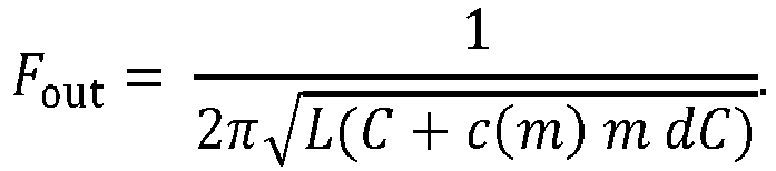
RF signal 104 frequency F out exhibits a non-linear relationship to the LC circuit capacitance Ctot.. - For simplicity, in this example, the capacitors of the LC circuit are represented as a base capacitance C, with a plurality of switchably connectable capacitors each having a capacitance dC, where an integer m, which may be positive, zero, or negative, represents the switchably connectable capacitors connected at a given moment, with the total capacitance in the LC circuit being

- The frequency of the
RF signal 104 output by theDCO 102 then becomes
- For controlling the RF frequency output by the
DCO 102, theDCO 102 comprises acontrol input 106, which may be a capacitor control code, i.e., a digital code indicating how capacitors should be switched into the LC circuit. - For controlling of modulation of the
RF signal 104 output by theDCO 102, theRF transmitter 100 comprisesdigital modulation circuitry 108 connected to theDCO 102. - The
digital modulation circuitry 108 comprises aninput 122 for inputting modulation data in the form of symbols for modulation. - The input is connected to a
data buffer 124 comprised in thedigital modulation circuitry 108 for buffering data to be modulated. - Further, the
digital modulation circuitry 108 comprises acompensation block 126 for compensating for LC non-linarity and modulation jitter, as will be described in detail below. Thecompensation block 126 is connected to thedata buffer 124 for receiving modulation symbols to be modulated and to amodulation block 128. - The
modulation block 128, comprised in thedigital modulation circuitry 108, converts the digital modulation symbols to acontrol word input 106 of theDCO 102. - The
RF signal 104 generated by theDCO 102 may, as shown inFig. 1 , be output to apower amplifier 110, as shown a switched-capacitor power amplifier 110, through a factor-of-2frequency divider 116. Thepower amplifier 110 may in turn output the signal, after amplification, to aload 114, for example an antenna, through abalun 112. - The
digital modulation circuitry 108 is driven, i.e., clocked, by anRF clock 118 derived from theRF signal 104 generated by theDCO 102. For example, as shown inFig. 1 , the output of the factor-of-2frequency divider 116 may be input to a further factor-of-8frequency divider 120, with the output of the factor-of-8divider 120 input to thedigital modulation block 110. Though further dividers (not shown) different parts of thedigital modulation circuitry 108 may comprise different respective clock domains driven by clock signals operating at different fractions of the frequency of the of theRF signal 104. - For example, the
digital modulation circuitry 108 may be configured for polar modulation of theRF signal 104, for example OFDM modulation. - In the example of
Fig. 1 , the DCO 102 operates at an approximate frequency of 4.8 GHz. Through the factor-of-2divider 116, the transmitted signal has an approximate frequency of 2.4 GHz and through the further factor-by-8divider 120, the digitallymodulation circuitry 108 is driven, i.e., clocked at a frequency of 300 MHz. - The
digital modulation circuitry 108 may oversample theRF signal 104 to be modulated. For example, for an oversampling factor of 10, the modulation data symbol rate will be 30 MHz. - Through the
digital modulation circuitry 108 being driven by theRF clock 118 derived fromRF signal 104 generated by theDCO 102, modulation data is input into theDCO 102 with aclock signal 118 which is derived from theDCO 102 itself. This means that when the RF signal 104 frequency generated by theDCO 102 goes up, the digital modulation data is input faster into theDCO 102 and when the RF signal 104 frequency generated by theDCO 102 goes down, the data is clocked slower into theDCO 102. In other words, the digital modulation data is clocked into theDCO 102 with a speed dependent on the content of the data, resulting in modulation jitter. - The compensation block in the
digital modulation circuitry 108 is configured to apply both a compensation for this modulation jitter due to thedigital modulation circuitry 108 being driven by theRF clock 118 and a compensation forDCO 102 non-linearity. - The compensation for modulation jitter and the compensation for
DCO 102 non-linearity may thus be applied in a single block, i.e., in a single circuit module without any intervening circuitry. - Further, the compensation for modulation jitter and the compensation for
DCO 102 non-linearity may be applied in a single step, or, alternatively in sequence. - The compensation is applied to the
control input 106 of theDCO 102. - A compensation factor to the frequency control of the
DCO 102 for compensating for modulation jitter may be derived as follows. - An ideal modulation phase advance delta per clock cycle of the
RF clock 118 driving thedigital modulation circuitry 108 can be written:
DCO 102 and F control is a deviation from the nominal RF frequency to which saidDCO 102 is modulated, i.e. the actual, modulated frequency of theDCO 102 is
DCO 102 and the frequency of theRF clock 118, as determined by thefrequency dividers - However, since the
RF clock 118 driving thedigital modulation circuitry 108 is derived from the RF signal 104 generated by theDCO 102, the actual phase advance per clock cycle of theRF clock 118 driving thedigital modulation circuitry 108 is:


- A compensation factor to the frequency control of the
DCO 102 for compensating both for modulation jitter and LC circuit non-linearity may be derived as follows. - As noted above, the frequency of the RF signal 104 generated by the
DCO 102 has a non-linear relationship to the connected capacitors m,



DCO 102 non-linearity:
digital modulation circuitry 108, or be calculated directly by thedigital modulation circuitry 108. - Hereby, a function already present in the
compensation module 126 to correct for frequency non-linearity, such as LC non-linearity, may be adapted to correct for modulation jitter as well. - The compensation for DCO non-linearity and the compensation for modulation jitter may work in opposite directions, so that the combined compensation implies not fully linearizing the frequency response of the DCO, with the remaining frequency non-linearity compensated for modulation jitter.
- For power efficiency the compensation may be done at the lowest resolution possible that still meets given EVM requirements. The compensation is done as close possible to the final control stage of the DCO, further decreasing required complexity and power requirements.
- In the above the inventive concept has mainly been described with reference to a limited number of examples. However, as is readily appreciated by a person skilled in the art, other examples than the ones disclosed above are equally possible within the scope of the inventive concept, as defined by the appended claims.
Claims (10)
- A radio frequency, RF, transmitter (100), comprising:a digitally controlled oscillator, DCO (102), configured to generate an RF signal (104); anddigital modulation circuitry (108) connected to said DCO (102) for modulation of said RF signal (104), and driven by an RF clock signal (118) derived from said RF signal (104),wherein said digital modulation circuitry (108) comprises a module (126) configured to apply a compensation for modulation jitter due to said modulation circuitry being driven by said RF clock signal and a compensation for DCO non-linearity.
- The RF transmitter of claim 1, wherein said compensation for modulation jitter and said compensation for DCO non-linearity are applied to a capacitor control (106) of said DCO (102).
- The RF transmitter of claim 2, wherein said compensation for modulation jitter can be written as a frequency compensation factor

- The RF transmitter (100) of any one of claims 1-3, wherein said compensation for modulation jitter and said compensation for DCO non-linearity are applied in a single step.
- The RF transmitter (100) of any one of claims 1-4, wherein said DCO non-linearity comprises an LC non-linearity.
- The RF transmitter (100) of any one of claims 4-5, wherein said compensation for modulation jitter and said compensation for DCO non-linearity can be written as a capacitance compensation factor


- The RF transmitter (100) of claim 3, wherein said capacitor control is a capacitor control code of said DCO (102).
- The RF transmitter (100) of any one of claims 1-7, wherein said digital modulation circuitry (108) is configured for polar modulation of said RF signal.
- The RF transmitter (100) of any one of claims 1-8, wherein said digital modulation circuitry oversamples said RF signal to be modulated.
- Method of generating a digitally-modulated a radio frequency, RF, signal (104), using an RF transmitter (100) comprising:a digitally controlled oscillator, DCO (102); anddigital modulation circuitry (108) connected to said DCO (102), said method comprising:generating, at said DCO (102), an RF signal (104);driving said digital modulation circuitry (108) by an RF clock signal (118) derived from said RF signal (104);inputting, at said modulation circuitry (108), symbols for modulation;applying, at said digital modulation circuitry (108), a compensation for modulation jitter due to said modulation circuitry being driven by said RF clock signal (104) and a compensation for DCO non-linearity; andmodulating said RF signal (104) as controlled by said digital modulation circuitry (108).
Priority Applications (2)
| Application Number | Priority Date | Filing Date | Title |
|---|---|---|---|
| EP19218401.8A EP3840225A1 (en) | 2019-12-20 | 2019-12-20 | Rf transmitter |
| US17/089,921 US11336314B2 (en) | 2019-12-20 | 2020-11-05 | RF transmitter |
Applications Claiming Priority (1)
| Application Number | Priority Date | Filing Date | Title |
|---|---|---|---|
| EP19218401.8A EP3840225A1 (en) | 2019-12-20 | 2019-12-20 | Rf transmitter |
Publications (1)
| Publication Number | Publication Date |
|---|---|
| EP3840225A1 true EP3840225A1 (en) | 2021-06-23 |
Family
ID=69411050
Family Applications (1)
| Application Number | Title | Priority Date | Filing Date |
|---|---|---|---|
| EP19218401.8A Pending EP3840225A1 (en) | 2019-12-20 | 2019-12-20 | Rf transmitter |
Country Status (2)
| Country | Link |
|---|---|
| US (1) | US11336314B2 (en) |
| EP (1) | EP3840225A1 (en) |
Citations (3)
| Publication number | Priority date | Publication date | Assignee | Title |
|---|---|---|---|---|
| WO1994006204A1 (en) * | 1992-09-02 | 1994-03-17 | Motorola, Inc. | Compensated digital frequency synthesizer |
| US20070189417A1 (en) * | 2006-02-15 | 2007-08-16 | Texas Instruments Incorporated | Precise delay alignment between amplitude and phase/frequency modulation paths in a digital polar transmitter |
| US20130301754A1 (en) * | 2012-05-10 | 2013-11-14 | Robert Bogdan Staszewski | Frequency modulator having digitally-controlled oscillator arranged for receiving modulation tuning word and phase-locked loop tuning word and/or receiving fractional tuning word obtained through asynchronous sampling and integer tuning word |
Family Cites Families (4)
| Publication number | Priority date | Publication date | Assignee | Title |
|---|---|---|---|---|
| WO2010029454A1 (en) | 2008-09-09 | 2010-03-18 | Nxp B.V. | Polar transmitter |
| US8476945B2 (en) * | 2011-03-23 | 2013-07-02 | International Business Machines Corporation | Phase profile generator |
| US8804874B2 (en) | 2012-01-20 | 2014-08-12 | Mediatek Inc. | Polar transmitter having digital processing block used for adjusting frequency modulating signal for frequency deviation of frequency modulated clock and related method thereof |
| US9270509B1 (en) | 2014-12-15 | 2016-02-23 | Apple Inc. | Devices and methods for orthogonal frequency division multiplexing signal phase shaping |
-
2019
- 2019-12-20 EP EP19218401.8A patent/EP3840225A1/en active Pending
-
2020
- 2020-11-05 US US17/089,921 patent/US11336314B2/en active Active
Patent Citations (3)
| Publication number | Priority date | Publication date | Assignee | Title |
|---|---|---|---|---|
| WO1994006204A1 (en) * | 1992-09-02 | 1994-03-17 | Motorola, Inc. | Compensated digital frequency synthesizer |
| US20070189417A1 (en) * | 2006-02-15 | 2007-08-16 | Texas Instruments Incorporated | Precise delay alignment between amplitude and phase/frequency modulation paths in a digital polar transmitter |
| US20130301754A1 (en) * | 2012-05-10 | 2013-11-14 | Robert Bogdan Staszewski | Frequency modulator having digitally-controlled oscillator arranged for receiving modulation tuning word and phase-locked loop tuning word and/or receiving fractional tuning word obtained through asynchronous sampling and integer tuning word |
Non-Patent Citations (1)
| Title |
|---|
| S. GUNTURIJ. TANGUDUS. RAMAKRISHNANJ. JANARDHANAND. SAHUS. MUKHERJEE: "Principal architectural changes in polar transmitter in DRP design for WLAN", 2013 NATIONAL CONFERENCE ON COMMUNICATIONS (NCC, 2013, pages 1 - 5, XP032350777, DOI: 10.1109/NCC.2013.6488006 |
Also Published As
| Publication number | Publication date |
|---|---|
| US20210194516A1 (en) | 2021-06-24 |
| US11336314B2 (en) | 2022-05-17 |
Similar Documents
| Publication | Publication Date | Title |
|---|---|---|
| US7929637B2 (en) | Method and apparatus for digital amplitude and phase modulation | |
| Ben-Bassat et al. | A fully integrated 27-dBm dual-band all-digital polar transmitter supporting 160 MHz for Wi-Fi 6 applications | |
| Ravi et al. | A 2.4-GHz 20–40-MHz channel WLAN digital outphasing transmitter utilizing a delay-based wideband phase modulator in 32-nm CMOS | |
| JP5227435B2 (en) | Integrated circuit, communication unit and method for improved amplitude resolution of RF-DAC | |
| US9444500B2 (en) | Modulation circuit of digital transmitter, digital transmitter, and signal modulation method | |
| US7817747B2 (en) | Precise delay alignment between amplitude and phase/frequency modulation paths in a digital polar transmitter | |
| US9130806B2 (en) | Wideband phase modulation methods and apparatus | |
| CN105577601B (en) | Circuit for VCO frequency adjustment, wireless communication unit and frequency generation method | |
| US20070189431A1 (en) | Delay alignment in a closed loop two-point modulation all digital phase locked loop | |
| US7289005B2 (en) | Polar modulator and a method for modulation of a signal | |
| Cruise et al. | A digital-to-RF-amplitude converter for GSM/GPRS/EDGE in 90-nm digital CMOS | |
| US20160322980A1 (en) | Wideband direct modulation with two-point injection in digital phase locked loops | |
| US8803627B1 (en) | Wideband direct DCO modulator with in-band compensation | |
| TWI513250B (en) | Digital transmitter and signal predistortion method thereof | |
| US20200220756A1 (en) | Systems and methods for maximizing power efficiency of a digital power amplifier in a polar transmitter | |
| US8855236B2 (en) | Digital amplitude modulation | |
| JP2006174464A (en) | Polar modulator and signal modulation method | |
| US9197161B2 (en) | Driving a mixer with a differential lo signal having at least three signal levels | |
| Buckel et al. | A highly reconfigurable RF-DPLL phase modulator for polar transmitters in cellular RFICs | |
| CN110830039A (en) | Control circuit, method and processing circuit of communication device | |
| US11336314B2 (en) | RF transmitter | |
| Choi et al. | A fully digital polar transmitter using a digital-to-time converter for high data rate system | |
| US20130259158A1 (en) | Very compact/linear software defined transmitter with digital modulator | |
| US10476517B2 (en) | Modulator for a digital amplifier | |
| Nidhi et al. | Design and analysis of a 1.8-GHz open-loop modulator for phase modulation and frequency synthesis using TDC-based calibration |
Legal Events
| Date | Code | Title | Description |
|---|---|---|---|
| PUAI | Public reference made under article 153(3) epc to a published international application that has entered the european phase |
Free format text: ORIGINAL CODE: 0009012 |
|
| STAA | Information on the status of an ep patent application or granted ep patent |
Free format text: STATUS: THE APPLICATION HAS BEEN PUBLISHED |
|
| AK | Designated contracting states |
Kind code of ref document: A1 Designated state(s): AL AT BE BG CH CY CZ DE DK EE ES FI FR GB GR HR HU IE IS IT LI LT LU LV MC MK MT NL NO PL PT RO RS SE SI SK SM TR |
|
| STAA | Information on the status of an ep patent application or granted ep patent |
Free format text: STATUS: REQUEST FOR EXAMINATION WAS MADE |
|
| 17P | Request for examination filed |
Effective date: 20211221 |
|
| RBV | Designated contracting states (corrected) |
Designated state(s): AL AT BE BG CH CY CZ DE DK EE ES FI FR GB GR HR HU IE IS IT LI LT LU LV MC MK MT NL NO PL PT RO RS SE SI SK SM TR |
|
| STAA | Information on the status of an ep patent application or granted ep patent |
Free format text: STATUS: EXAMINATION IS IN PROGRESS |
|
| 17Q | First examination report despatched |
Effective date: 20241211 |