EP3840114A1 - Semiconductor device with waveguide and method therefor - Google Patents
Semiconductor device with waveguide and method therefor Download PDFInfo
- Publication number
- EP3840114A1 EP3840114A1 EP20212279.2A EP20212279A EP3840114A1 EP 3840114 A1 EP3840114 A1 EP 3840114A1 EP 20212279 A EP20212279 A EP 20212279A EP 3840114 A1 EP3840114 A1 EP 3840114A1
- Authority
- EP
- European Patent Office
- Prior art keywords
- launcher
- waveguide
- substrate
- assembly
- antenna
- Prior art date
- Legal status (The legal status is an assumption and is not a legal conclusion. Google has not performed a legal analysis and makes no representation as to the accuracy of the status listed.)
- Granted
Links
Images









Classifications
-
- G—PHYSICS
- G01—MEASURING; TESTING
- G01S—RADIO DIRECTION-FINDING; RADIO NAVIGATION; DETERMINING DISTANCE OR VELOCITY BY USE OF RADIO WAVES; LOCATING OR PRESENCE-DETECTING BY USE OF THE REFLECTION OR RERADIATION OF RADIO WAVES; ANALOGOUS ARRANGEMENTS USING OTHER WAVES
- G01S7/00—Details of systems according to groups G01S13/00, G01S15/00, G01S17/00
- G01S7/02—Details of systems according to groups G01S13/00, G01S15/00, G01S17/00 of systems according to group G01S13/00
- G01S7/03—Details of HF subsystems specially adapted therefor, e.g. common to transmitter and receiver
- G01S7/032—Constructional details for solid-state radar subsystems
-
- H—ELECTRICITY
- H01—ELECTRIC ELEMENTS
- H01P—WAVEGUIDES; RESONATORS, LINES, OR OTHER DEVICES OF THE WAVEGUIDE TYPE
- H01P3/00—Waveguides; Transmission lines of the waveguide type
- H01P3/12—Hollow waveguides
- H01P3/121—Hollow waveguides integrated in a substrate
-
- H—ELECTRICITY
- H01—ELECTRIC ELEMENTS
- H01Q—ANTENNAS, i.e. RADIO AERIALS
- H01Q1/00—Details of, or arrangements associated with, antennas
- H01Q1/12—Supports; Mounting means
- H01Q1/22—Supports; Mounting means by structural association with other equipment or articles
- H01Q1/2283—Supports; Mounting means by structural association with other equipment or articles mounted in or on the surface of a semiconductor substrate as a chip-type antenna or integrated with other components into an IC package
-
- H—ELECTRICITY
- H01—ELECTRIC ELEMENTS
- H01Q—ANTENNAS, i.e. RADIO AERIALS
- H01Q1/00—Details of, or arrangements associated with, antennas
- H01Q1/50—Structural association of antennas with earthing switches, lead-in devices or lightning protectors
-
- H—ELECTRICITY
- H01—ELECTRIC ELEMENTS
- H01Q—ANTENNAS, i.e. RADIO AERIALS
- H01Q13/00—Waveguide horns or mouths; Slot antennas; Leaky-waveguide antennas; Equivalent structures causing radiation along the transmission path of a guided wave
- H01Q13/06—Waveguide mouths
-
- H—ELECTRICITY
- H01—ELECTRIC ELEMENTS
- H01Q—ANTENNAS, i.e. RADIO AERIALS
- H01Q21/00—Antenna arrays or systems
- H01Q21/0087—Apparatus or processes specially adapted for manufacturing antenna arrays
-
- H—ELECTRICITY
- H01—ELECTRIC ELEMENTS
- H01Q—ANTENNAS, i.e. RADIO AERIALS
- H01Q21/00—Antenna arrays or systems
- H01Q21/06—Arrays of individually energised antenna units similarly polarised and spaced apart
- H01Q21/061—Two dimensional planar arrays
- H01Q21/064—Two dimensional planar arrays using horn or slot aerials
-
- H—ELECTRICITY
- H10—SEMICONDUCTOR DEVICES; ELECTRIC SOLID-STATE DEVICES NOT OTHERWISE PROVIDED FOR
- H10P—GENERIC PROCESSES OR APPARATUS FOR THE MANUFACTURE OR TREATMENT OF DEVICES COVERED BY CLASS H10
- H10P72/00—Handling or holding of wafers, substrates or devices during manufacture or treatment thereof
- H10P72/70—Handling or holding of wafers, substrates or devices during manufacture or treatment thereof for supporting or gripping
- H10P72/74—Handling or holding of wafers, substrates or devices during manufacture or treatment thereof for supporting or gripping using temporarily an auxiliary support
-
- H—ELECTRICITY
- H10—SEMICONDUCTOR DEVICES; ELECTRIC SOLID-STATE DEVICES NOT OTHERWISE PROVIDED FOR
- H10W—GENERIC PACKAGES, INTERCONNECTIONS, CONNECTORS OR OTHER CONSTRUCTIONAL DETAILS OF DEVICES COVERED BY CLASS H10
- H10W44/00—Electrical arrangements for controlling or matching impedance
- H10W44/20—Electrical arrangements for controlling or matching impedance at high-frequency [HF] or radio frequency [RF]
-
- H—ELECTRICITY
- H10—SEMICONDUCTOR DEVICES; ELECTRIC SOLID-STATE DEVICES NOT OTHERWISE PROVIDED FOR
- H10W—GENERIC PACKAGES, INTERCONNECTIONS, CONNECTORS OR OTHER CONSTRUCTIONAL DETAILS OF DEVICES COVERED BY CLASS H10
- H10W70/00—Package substrates; Interposers; Redistribution layers [RDL]
- H10W70/01—Manufacture or treatment
- H10W70/05—Manufacture or treatment of insulating or insulated package substrates, or of interposers, or of redistribution layers
-
- H—ELECTRICITY
- H10—SEMICONDUCTOR DEVICES; ELECTRIC SOLID-STATE DEVICES NOT OTHERWISE PROVIDED FOR
- H10W—GENERIC PACKAGES, INTERCONNECTIONS, CONNECTORS OR OTHER CONSTRUCTIONAL DETAILS OF DEVICES COVERED BY CLASS H10
- H10W70/00—Package substrates; Interposers; Redistribution layers [RDL]
- H10W70/01—Manufacture or treatment
- H10W70/05—Manufacture or treatment of insulating or insulated package substrates, or of interposers, or of redistribution layers
- H10W70/08—Manufacture or treatment of insulating or insulated package substrates, or of interposers, or of redistribution layers by depositing layers on the chip or wafer, e.g. "chip-first" RDLs
- H10W70/09—Manufacture or treatment of insulating or insulated package substrates, or of interposers, or of redistribution layers by depositing layers on the chip or wafer, e.g. "chip-first" RDLs extending onto an encapsulation that laterally surrounds the chip or wafer, e.g. fan-out wafer level package [FOWLP] RDLs
-
- H—ELECTRICITY
- H10—SEMICONDUCTOR DEVICES; ELECTRIC SOLID-STATE DEVICES NOT OTHERWISE PROVIDED FOR
- H10W—GENERIC PACKAGES, INTERCONNECTIONS, CONNECTORS OR OTHER CONSTRUCTIONAL DETAILS OF DEVICES COVERED BY CLASS H10
- H10W70/00—Package substrates; Interposers; Redistribution layers [RDL]
- H10W70/01—Manufacture or treatment
- H10W70/05—Manufacture or treatment of insulating or insulated package substrates, or of interposers, or of redistribution layers
- H10W70/093—Connecting or disconnecting other interconnections thereto or therefrom, e.g. connecting bond wires or bumps
-
- H—ELECTRICITY
- H10—SEMICONDUCTOR DEVICES; ELECTRIC SOLID-STATE DEVICES NOT OTHERWISE PROVIDED FOR
- H10W—GENERIC PACKAGES, INTERCONNECTIONS, CONNECTORS OR OTHER CONSTRUCTIONAL DETAILS OF DEVICES COVERED BY CLASS H10
- H10W70/00—Package substrates; Interposers; Redistribution layers [RDL]
- H10W70/60—Insulating or insulated package substrates; Interposers; Redistribution layers
-
- H—ELECTRICITY
- H10—SEMICONDUCTOR DEVICES; ELECTRIC SOLID-STATE DEVICES NOT OTHERWISE PROVIDED FOR
- H10W—GENERIC PACKAGES, INTERCONNECTIONS, CONNECTORS OR OTHER CONSTRUCTIONAL DETAILS OF DEVICES COVERED BY CLASS H10
- H10W70/00—Package substrates; Interposers; Redistribution layers [RDL]
- H10W70/60—Insulating or insulated package substrates; Interposers; Redistribution layers
- H10W70/611—Insulating or insulated package substrates; Interposers; Redistribution layers for connecting multiple chips together
-
- H—ELECTRICITY
- H10—SEMICONDUCTOR DEVICES; ELECTRIC SOLID-STATE DEVICES NOT OTHERWISE PROVIDED FOR
- H10W—GENERIC PACKAGES, INTERCONNECTIONS, CONNECTORS OR OTHER CONSTRUCTIONAL DETAILS OF DEVICES COVERED BY CLASS H10
- H10W70/00—Package substrates; Interposers; Redistribution layers [RDL]
- H10W70/60—Insulating or insulated package substrates; Interposers; Redistribution layers
- H10W70/611—Insulating or insulated package substrates; Interposers; Redistribution layers for connecting multiple chips together
- H10W70/614—Insulating or insulated package substrates; Interposers; Redistribution layers for connecting multiple chips together the multiple chips being integrally enclosed
-
- H—ELECTRICITY
- H10—SEMICONDUCTOR DEVICES; ELECTRIC SOLID-STATE DEVICES NOT OTHERWISE PROVIDED FOR
- H10W—GENERIC PACKAGES, INTERCONNECTIONS, CONNECTORS OR OTHER CONSTRUCTIONAL DETAILS OF DEVICES COVERED BY CLASS H10
- H10W70/00—Package substrates; Interposers; Redistribution layers [RDL]
- H10W70/60—Insulating or insulated package substrates; Interposers; Redistribution layers
- H10W70/62—Insulating or insulated package substrates; Interposers; Redistribution layers characterised by their interconnections
- H10W70/65—Shapes or dispositions of interconnections
-
- H—ELECTRICITY
- H10—SEMICONDUCTOR DEVICES; ELECTRIC SOLID-STATE DEVICES NOT OTHERWISE PROVIDED FOR
- H10W—GENERIC PACKAGES, INTERCONNECTIONS, CONNECTORS OR OTHER CONSTRUCTIONAL DETAILS OF DEVICES COVERED BY CLASS H10
- H10W70/00—Package substrates; Interposers; Redistribution layers [RDL]
- H10W70/60—Insulating or insulated package substrates; Interposers; Redistribution layers
- H10W70/67—Insulating or insulated package substrates; Interposers; Redistribution layers characterised by their insulating layers or insulating parts
- H10W70/68—Shapes or dispositions thereof
-
- H—ELECTRICITY
- H10—SEMICONDUCTOR DEVICES; ELECTRIC SOLID-STATE DEVICES NOT OTHERWISE PROVIDED FOR
- H10W—GENERIC PACKAGES, INTERCONNECTIONS, CONNECTORS OR OTHER CONSTRUCTIONAL DETAILS OF DEVICES COVERED BY CLASS H10
- H10W70/00—Package substrates; Interposers; Redistribution layers [RDL]
- H10W70/60—Insulating or insulated package substrates; Interposers; Redistribution layers
- H10W70/67—Insulating or insulated package substrates; Interposers; Redistribution layers characterised by their insulating layers or insulating parts
- H10W70/68—Shapes or dispositions thereof
- H10W70/685—Shapes or dispositions thereof comprising multiple insulating layers
-
- H—ELECTRICITY
- H10—SEMICONDUCTOR DEVICES; ELECTRIC SOLID-STATE DEVICES NOT OTHERWISE PROVIDED FOR
- H10W—GENERIC PACKAGES, INTERCONNECTIONS, CONNECTORS OR OTHER CONSTRUCTIONAL DETAILS OF DEVICES COVERED BY CLASS H10
- H10W74/00—Encapsulations, e.g. protective coatings
- H10W74/01—Manufacture or treatment
- H10W74/016—Manufacture or treatment using moulds
-
- H—ELECTRICITY
- H10—SEMICONDUCTOR DEVICES; ELECTRIC SOLID-STATE DEVICES NOT OTHERWISE PROVIDED FOR
- H10W—GENERIC PACKAGES, INTERCONNECTIONS, CONNECTORS OR OTHER CONSTRUCTIONAL DETAILS OF DEVICES COVERED BY CLASS H10
- H10W74/00—Encapsulations, e.g. protective coatings
- H10W74/01—Manufacture or treatment
- H10W74/019—Manufacture or treatment using temporary auxiliary substrates
-
- H—ELECTRICITY
- H10—SEMICONDUCTOR DEVICES; ELECTRIC SOLID-STATE DEVICES NOT OTHERWISE PROVIDED FOR
- H10W—GENERIC PACKAGES, INTERCONNECTIONS, CONNECTORS OR OTHER CONSTRUCTIONAL DETAILS OF DEVICES COVERED BY CLASS H10
- H10W74/00—Encapsulations, e.g. protective coatings
- H10W74/10—Encapsulations, e.g. protective coatings characterised by their shape or disposition
- H10W74/111—Encapsulations, e.g. protective coatings characterised by their shape or disposition the semiconductor body being completely enclosed
- H10W74/114—Encapsulations, e.g. protective coatings characterised by their shape or disposition the semiconductor body being completely enclosed by a substrate and the encapsulations
- H10W74/117—Encapsulations, e.g. protective coatings characterised by their shape or disposition the semiconductor body being completely enclosed by a substrate and the encapsulations the substrate having spherical bumps for external connection
-
- H—ELECTRICITY
- H10—SEMICONDUCTOR DEVICES; ELECTRIC SOLID-STATE DEVICES NOT OTHERWISE PROVIDED FOR
- H10W—GENERIC PACKAGES, INTERCONNECTIONS, CONNECTORS OR OTHER CONSTRUCTIONAL DETAILS OF DEVICES COVERED BY CLASS H10
- H10W90/00—Package configurations
- H10W90/401—Package configurations characterised by multiple insulating or insulated package substrates, interposers or RDLs
-
- G—PHYSICS
- G01—MEASURING; TESTING
- G01S—RADIO DIRECTION-FINDING; RADIO NAVIGATION; DETERMINING DISTANCE OR VELOCITY BY USE OF RADIO WAVES; LOCATING OR PRESENCE-DETECTING BY USE OF THE REFLECTION OR RERADIATION OF RADIO WAVES; ANALOGOUS ARRANGEMENTS USING OTHER WAVES
- G01S13/00—Systems using the reflection or reradiation of radio waves, e.g. radar systems; Analogous systems using reflection or reradiation of waves whose nature or wavelength is irrelevant or unspecified
- G01S13/88—Radar or analogous systems specially adapted for specific applications
- G01S13/93—Radar or analogous systems specially adapted for specific applications for anti-collision purposes
- G01S13/931—Radar or analogous systems specially adapted for specific applications for anti-collision purposes of land vehicles
-
- H—ELECTRICITY
- H10—SEMICONDUCTOR DEVICES; ELECTRIC SOLID-STATE DEVICES NOT OTHERWISE PROVIDED FOR
- H10P—GENERIC PROCESSES OR APPARATUS FOR THE MANUFACTURE OR TREATMENT OF DEVICES COVERED BY CLASS H10
- H10P72/00—Handling or holding of wafers, substrates or devices during manufacture or treatment thereof
- H10P72/70—Handling or holding of wafers, substrates or devices during manufacture or treatment thereof for supporting or gripping
- H10P72/74—Handling or holding of wafers, substrates or devices during manufacture or treatment thereof for supporting or gripping using temporarily an auxiliary support
- H10P72/7436—Handling or holding of wafers, substrates or devices during manufacture or treatment thereof for supporting or gripping using temporarily an auxiliary support used to support a device or a wafer when forming electrical connections thereto
-
- H—ELECTRICITY
- H10—SEMICONDUCTOR DEVICES; ELECTRIC SOLID-STATE DEVICES NOT OTHERWISE PROVIDED FOR
- H10W—GENERIC PACKAGES, INTERCONNECTIONS, CONNECTORS OR OTHER CONSTRUCTIONAL DETAILS OF DEVICES COVERED BY CLASS H10
- H10W44/00—Electrical arrangements for controlling or matching impedance
- H10W44/20—Electrical arrangements for controlling or matching impedance at high-frequency [HF] or radio frequency [RF]
- H10W44/203—Electrical connections
- H10W44/216—Waveguides, e.g. strip lines
-
- H—ELECTRICITY
- H10—SEMICONDUCTOR DEVICES; ELECTRIC SOLID-STATE DEVICES NOT OTHERWISE PROVIDED FOR
- H10W—GENERIC PACKAGES, INTERCONNECTIONS, CONNECTORS OR OTHER CONSTRUCTIONAL DETAILS OF DEVICES COVERED BY CLASS H10
- H10W44/00—Electrical arrangements for controlling or matching impedance
- H10W44/20—Electrical arrangements for controlling or matching impedance at high-frequency [HF] or radio frequency [RF]
- H10W44/241—Electrical arrangements for controlling or matching impedance at high-frequency [HF] or radio frequency [RF] for passive devices or passive elements
- H10W44/248—Electrical arrangements for controlling or matching impedance at high-frequency [HF] or radio frequency [RF] for passive devices or passive elements for antennas
-
- H—ELECTRICITY
- H10—SEMICONDUCTOR DEVICES; ELECTRIC SOLID-STATE DEVICES NOT OTHERWISE PROVIDED FOR
- H10W—GENERIC PACKAGES, INTERCONNECTIONS, CONNECTORS OR OTHER CONSTRUCTIONAL DETAILS OF DEVICES COVERED BY CLASS H10
- H10W70/00—Package substrates; Interposers; Redistribution layers [RDL]
- H10W70/60—Insulating or insulated package substrates; Interposers; Redistribution layers
- H10W70/62—Insulating or insulated package substrates; Interposers; Redistribution layers characterised by their interconnections
- H10W70/65—Shapes or dispositions of interconnections
- H10W70/652—Cross-sectional shapes
- H10W70/6528—Cross-sectional shapes of the portions that connect to chips, wafers or package parts
-
- H—ELECTRICITY
- H10—SEMICONDUCTOR DEVICES; ELECTRIC SOLID-STATE DEVICES NOT OTHERWISE PROVIDED FOR
- H10W—GENERIC PACKAGES, INTERCONNECTIONS, CONNECTORS OR OTHER CONSTRUCTIONAL DETAILS OF DEVICES COVERED BY CLASS H10
- H10W72/00—Interconnections or connectors in packages
- H10W72/20—Bump connectors, e.g. solder bumps or copper pillars; Dummy bumps; Thermal bumps
- H10W72/241—Dispositions, e.g. layouts
-
- H—ELECTRICITY
- H10—SEMICONDUCTOR DEVICES; ELECTRIC SOLID-STATE DEVICES NOT OTHERWISE PROVIDED FOR
- H10W—GENERIC PACKAGES, INTERCONNECTIONS, CONNECTORS OR OTHER CONSTRUCTIONAL DETAILS OF DEVICES COVERED BY CLASS H10
- H10W74/00—Encapsulations, e.g. protective coatings
- H10W74/10—Encapsulations, e.g. protective coatings characterised by their shape or disposition
- H10W74/131—Encapsulations, e.g. protective coatings characterised by their shape or disposition the semiconductor body being only partially enclosed
- H10W74/142—Encapsulations, e.g. protective coatings characterised by their shape or disposition the semiconductor body being only partially enclosed the encapsulations exposing the passive side of the semiconductor body
-
- H—ELECTRICITY
- H10—SEMICONDUCTOR DEVICES; ELECTRIC SOLID-STATE DEVICES NOT OTHERWISE PROVIDED FOR
- H10W—GENERIC PACKAGES, INTERCONNECTIONS, CONNECTORS OR OTHER CONSTRUCTIONAL DETAILS OF DEVICES COVERED BY CLASS H10
- H10W90/00—Package configurations
-
- H—ELECTRICITY
- H10—SEMICONDUCTOR DEVICES; ELECTRIC SOLID-STATE DEVICES NOT OTHERWISE PROVIDED FOR
- H10W—GENERIC PACKAGES, INTERCONNECTIONS, CONNECTORS OR OTHER CONSTRUCTIONAL DETAILS OF DEVICES COVERED BY CLASS H10
- H10W90/00—Package configurations
- H10W90/701—Package configurations characterised by the relative positions of pads or connectors relative to package parts
Definitions
- This disclosure relates generally to semiconductor device packaging, and more specifically, to a semiconductor device with waveguide and method of forming the same.
- a semiconductor device including a packaged assembly with overlapping waveguide structure affixed to a common substrate.
- the waveguide structure is physically decoupled from the packaged assembly.
- a semiconductor die and launcher structure are encapsulated on a package substrate to form the packaged assembly.
- the waveguide structure includes a waveguide opening over an antenna launcher of the launcher structure allowing propagation of radio frequency (RF) signals.
- RF radio frequency
- FIG. 1 illustrates, in a simplified cross-sectional view, an example assembly of an example semiconductor device with waveguide 100 along line A-A of FIG. 5 at a stage of manufacture in accordance with an embodiment.
- the assembly of semiconductor device 100 includes a semiconductor die 102 and launcher structures 106 and 108 placed on a carrier substrate 104.
- the launcher structures 106 and 108 are each formed as a multilayer laminate structure having a cavity (e.g., cavities 112 and 114).
- launcher structure 106 includes conductive layers 122 and 130 (e.g., metal or other conductive material layers) separated by a non-conductive material 120 (e.g., FR-4, ceramic).
- Contacts 124 and vias 126 provide conductive connections between terminal pads 132 at a bottom surface of launcher structure 106 and conductive layers 122 and 130.
- the cavity 112 includes an antenna launcher 116 located at a bottom surface of the cavity 112.
- the cavity 114 includes an antenna launcher 118 located at a bottom surface of the cavity 114.
- the antenna launcher 116 is connected to terminal pad 134 at the bottom surface of launcher structure 106 by way of interconnecting contacts and via (e.g., contacts 124, via 126). Via plugs 128 may be incorporated in vias 126 to provide additional strength and rigidity.
- conductive layers 122 and interconnecting contacts 124 are configured and arranged to serve as a conductive wall or fence substantially surrounding the antenna launcher 116. In some embodiments, it may be desirable to connect the conductive wall or fence to a ground supply terminal or other supply terminal.
- conductive layer 130 is configured and arranged to serve as a signal reflector located below the antenna launcher 116 and substantially surrounding the via interconnecting the antenna launcher 116 with the terminal pad 134. In some embodiments, it may be desirable to form the signal reflector on a next conductive layer immediately below the antenna launcher 116.
- the semiconductor die 102 has an active surface (e.g., major surface having circuitry) and a backside surface (e.g., major surface opposite of the active surface).
- the semiconductor die 102 includes bond pads 110 at the active surface configured for connection to antenna launchers 116 and 118 by way of a redistribution layer (RDL), for example.
- RDL redistribution layer
- the semiconductor die 102 may be formed from any suitable semiconductor material, such as silicon, germanium, gallium arsenide, gallium nitride and the like.
- Semiconductor die 102 may further include any digital circuits, analog circuits, RF circuits, memory, signal processor, MEMS, sensors, the like, and combinations thereof.
- FIG. 2 illustrates, in a simplified cross-sectional view, the example assembly at a subsequent stage of manufacture in accordance with an embodiment.
- the assembly of semiconductor device 100 includes an encapsulant (e.g., epoxy material) 204 at least partially encapsulating semiconductor die 102 and launcher structures 106 and 108 placed on the carrier substrate 104.
- the semiconductor die 102 and launcher structures 106 and 108 are over-molded with an epoxy material encapsulant by way of a film-assisted molding (FAM) process.
- a FAM tool 202 is in contact with a top surface of the launcher structures 106 and 108 while molding to keep predetermined portions (e.g., cavities 112 and 114) clear of encapsulant (e.g., not encapsulated).
- FIG. 3 illustrates, in a simplified cross-sectional view, the example assembly at a subsequent stage of manufacture in accordance with an embodiment.
- the assembly 302 includes an encapsulant 204 at least partially encapsulating semiconductor die 102 and launcher structures 106 and 108 along with an RDL substrate 304 and ball connectors 310.
- the RDL substrate 304 is applied to the resulting exposed bottom surface including an exposed active surface of the semiconductor die 102 and exposed bottom surfaces of the launcher structures 106 and 108.
- Conductive feeds 306 and 308 are formed in the RDL substrate 304 between bond pads 110 and terminal pads 134 to interconnect semiconductor die 102 and antenna launchers 116 and 118 respectively.
- conductive ball connectors 310 e.g., solder balls
- the ball connectors 310 are configured and arranged to provide conductive connections between the assembly 302 and a printed circuit board (PCB), for example.
- Ball connectors 310 may be any suitable conductive structure such as solder ball, gold studs, copper pillars, and the like, to connect conductive features of the assembly 302 with the PCB.
- the RDL substrate 304 is formed as a build-up substrate including a redistribution layer.
- the RDL substrate 304 may be formed as a pre-formed substrate including a redistribution layer.
- ball connectors 310 may be directly affixed to terminal pads 132, 134 and bond pads 110 to provide connectivity with a PCB, for example, without utilizing an RDL substrate.
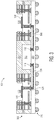
- FIG. 4 illustrates, in a simplified cross-sectional view, the example semiconductor device with waveguide 100 along line A-A of FIG. 5 at a stage of manufacture in accordance with an embodiment.
- the semiconductor device 100 includes the assembly 302 and overlapping waveguide structure 402 affixed to a common substrate 404. With the assembly 302 and overlapping waveguide structure 402 affixed to the substrate 404, the waveguide structure 402 is physically decoupled from the assembly 302. For example, the waveguide structure 402 does not physically contact the assembly 302.
- substrate 404 may be characterized as a PCB or other multilayer substrate configured to provide connectivity with other components of a system, for example.
- the waveguide structure 402 includes waveguides 406 (e.g., waveguide openings) and is attached to the substrate 404 at interface surfaces 408.
- the waveguide structure 402 may be attached to the substrate 404 at interface surfaces 408 using screws, alignment pins, adhesives, and combinations thereof, for example.
- the waveguide structure 402 is formed from a conductive material such as a metal (e.g., aluminum, copper), non-conductive material coated with conductive material, other conductive materials, or combinations thereof.
- Waveguides 406 are formed as waveguide openings in the waveguide structure 402 with antenna launchers 116 and 118 exposed through the openings.
- the waveguide openings 406 include sidewall portions 410 which extend downward into the cavities 112 and 114 and substantially surrounding the antenna launchers 116 and 118 respectively.
- Waveguides 406 dimensions may be configured for propagation of signals (e.g., radar, mmWave signals, 30 GHz to 300 GHz) having desired wavelengths.
- signals e.g., radar, mmWave signals, 30 GHz to 300 GHz
- a waveguide may be configured for propagation (e.g., transmission) of a radar signal having a frequency of 77 GHz. Because a 77 GHz signal has a wavelength of approximately 4 mm, the waveguide is configured having a width dimension of approximately 2 mm, or half of the desired wavelength.
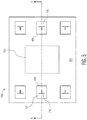
- FIG. 5 illustrates, in a plan view, the example semiconductor device with waveguide 100 at the stage of manufacture depicted in FIG. 4 in accordance with an embodiment.
- the semiconductor device 100 includes the assembly (302) and overlapping waveguide structure 402 affixed to a common substrate (404). Underlying semiconductor die 102 is shown as dashed outline labeled 102 for reference.
- Cross-sectional views of semiconductor device 100 taken along line A-A including waveguides 406 are shown in example stages of manufacture depicted in FIG. 1 through FIG. 4 .
- Waveguides 406 are formed as waveguide openings in the waveguide structure 402 with antenna launchers 116 and 118 and non-conductive material 120 of launcher structures 106 and 108 exposed through the respective openings.
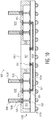
- FIG. 6 illustrates, in a simplified cross-sectional view, an example assembly of an example semiconductor device with waveguide 200 along line B-B of FIG. 8 at a stage of manufacture in accordance with an embodiment.
- the assembly 600 includes an encapsulant 638 at least partially encapsulating semiconductor die 602 and launcher structures 606 and 608 along with an RDL substrate 604 and ball connectors 644.
- Conductive feeds 640 and 642 are formed in the RDL substrate 604 between bond pads 610 and terminal pads 634 to interconnect semiconductor die 602 and antenna launchers 616 and 618 respectively.
- Conductive ball connectors 644 e.g., solder balls
- the ball connectors 644 are configured and arranged to provide conductive connections between the assembly 600 and a PCB, for example.
- Ball connectors 644 may be any suitable conductive structure such as solder balls, gold studs, copper pillars, and the like, to connect conductive features of the assembly 600 with the PCB.
- the RDL substrate 604 is formed as a build-up substrate including a redistribution layer.
- the RDL substrate 604 may be formed as a pre-formed substrate including a redistribution layer.
- ball connectors 644 may be directly affixed to terminal pads 632-634 and bond pads 610 to provide connectivity with a PCB, for example, without utilizing an RDL substrate.
- the launcher structures 606 and 608 are each formed as a multilayer laminate structure having a cavity (e.g., cavities 612 and 614).
- launcher structure 606 includes conductive layers 622 (e.g., metal or other conductive material layers) separated by a non-conductive material 620 (e.g., FR-4, ceramic).
- Contacts 624 and vias 625 provide conductive connections between terminal pads 632 at a bottom surface of launcher structure 606 and conductive layers 622.
- the cavity 612 includes an antenna launcher 616 and surrounding conductive pad 630 located at a bottom surface of the cavity 612.
- the cavity 614 includes an antenna launcher 618 and surrounding conductive pad located at a bottom surface of the cavity 614.
- a conductive ring 626 is attached to the conductive pad 630 by way of a conductive connector 628 (e.g., solder, electrically conductive adhesive, anisotropic conductive film).
- a channel 636 is formed in the cavity 612 between outer sidewall of the conductive ring 626 and sidewall of cavity 612.
- the antenna launcher 616 is connected to terminal pad 634 at the bottom surface of launcher structure 606 by way of interconnecting contacts and via.
- conductive layers 622 and interconnecting contacts 624 are configured and arranged to serve as a conductive wall or fence substantially surrounding the sidewall of cavity 612. In some embodiments, it may be desirable to connect the conductive wall or fence to a ground supply terminal or other supply terminal.
- the semiconductor die 602 has an active surface (e.g., major surface having circuitry) and a backside surface (e.g., major surface opposite of the active surface).
- the semiconductor die 602 includes bond pads 610 at the active surface configured for connection to antenna launchers 616 and 618 by way of an RDL, for example.
- the semiconductor die 602 may be formed from any suitable semiconductor material, such as silicon, germanium, gallium arsenide, gallium nitride and the like.
- Semiconductor die 602 may further include any digital circuits, analog circuits, RF circuits, memory, signal processor, MEMS, sensors, the like, and combinations thereof.
- FIG. 7 illustrates, in a simplified cross-sectional view, the example semiconductor device 200 along line B-B of FIG. 8 at a stage of manufacture in accordance with an embodiment.
- the semiconductor device 200 includes the assembly 600 and overlapping waveguide structure 702 affixed to a common substrate 704. With the assembly 600 and overlapping waveguide structure 702 affixed to the substrate 704, the waveguide structure 702 is physically decoupled from the assembly 600. For example, the waveguide structure 702 does not physically contact the assembly 600.
- substrate 704 may be characterized as a PCB or other multilayer substrate configured to provide connectivity with other components of a system, for example.
- the waveguide structure 702 includes waveguides 706 (e.g., waveguide openings) and is attached to the substrate 704 at interface surfaces 708.
- the waveguide structure 702 may be attached to the substrate 704 at interface surfaces 708 using screws, alignment pins, adhesives, and combinations thereof, for example.
- the waveguide structure 702 is formed from a conductive material such as a metal (e.g., aluminum, copper), other conductive materials, or combinations thereof.
- Waveguides 706 are formed as waveguide openings in the waveguide structure 702 with antenna launchers 616 and 618 exposed through the openings.
- the waveguide openings 706 include sidewall portions 710 which extend downward into the channels 636 formed in the cavities 612 and 614 between outer sidewall of the conductive rings 626 and sidewall of cavities 612 and 614 respectively.
- Waveguides 706 dimensions e.g., width, length
- signals e.g., radar, mmWave signals, 30 GHz to 300 GHz
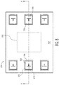
- FIG. 8 illustrates, in a plan view, the example semiconductor device with waveguide 200 at the stage of manufacture depicted in FIG. 7 in accordance with an embodiment.
- the semiconductor device 200 includes the assembly (600) and overlapping waveguide structure 702 affixed to a common substrate (704). Underlying semiconductor die 602 is shown as dashed outline labeled 602 for reference.
- Cross-sectional views of semiconductor device with waveguide 200 taken along line B-B including waveguides 706 are shown in example stages of manufacture depicted in FIG. 7 and FIG. 8 .
- Waveguides 706 are formed as waveguide openings in the waveguide structure 702 with antenna launchers 616 and 618, conductive rings 626, and non-conductive material 620 of launcher structures 606 and 608 exposed through the respective openings.
- FIG. 9 illustrates, in a simplified cross-sectional view, an example assembly of an example semiconductor device with waveguide 300 along line C-C of FIG. 12 at a stage of manufacture in accordance with an embodiment.
- the assembly of semiconductor device 300 includes an encapsulant (e.g., epoxy material) 928 encapsulating semiconductor die 902 and launcher structures 906 and 908 placed on the carrier substrate 904.
- the semiconductor die 902 and launcher structures 906 and 908 are over-molded with an epoxy material encapsulant.
- the launcher structures 906 and 908 are formed as laminate structures having antenna launcher 914 and 916 located at a top surface of launcher structures 906 and 908 respectively.
- the launcher structure 906 includes conductive interconnects 918 and 920 (e.g., metal or other conductive materials) separated by a non-conductive material 912 (e.g., FR-4, ceramic).
- Conductive interconnect 918 provides conductive connections between terminal pads 922 at a bottom surface of launcher structure 906 and conductive ball connectors 926 (e.g., solder balls).
- the antenna launcher 914 is connected to terminal pad 924 at the bottom surface of launcher structure 906 by way of conductive interconnect 920.
- Conductive interconnect 918 and conductive ball connectors 926 are configured and arranged to substantially surround antennal launcher 914 and conductive interconnect 920.
- the semiconductor die 902 has an active surface (e.g., major surface having circuitry) and a backside surface (e.g., major surface opposite of the active surface).
- the semiconductor die 902 includes bond pads 910 at the active surface configured for connection to antenna launchers 914 and 916 by way of an RDL, for example.
- the semiconductor die 902 may be formed from any suitable semiconductor material, such as silicon, germanium, gallium arsenide, gallium nitride and the like.
- Semiconductor die 902 may further include any digital circuits, analog circuits, RF circuits, memory, signal processor, MEMS, sensors, the like, and combinations thereof.
- FIG. 10 illustrates, in a simplified cross-sectional view, the example assembly at a subsequent stage of manufacture in accordance with an embodiment.
- the assembly 1000 includes the encapsulant 928 at least partially encapsulating semiconductor die 902 and launcher structures 906 and 908 along with an RDL substrate 1004 and ball connectors 1016.
- a backside grind operation is performed on the assembly 1000 to expose portions of ball connectors 926 of launcher structures 906 and 908 and a backside surface of semiconductor die 902.
- a conductive ring 1008 is attached to a conductive path formed by the exposed a portions of ball connectors 926 by way of a conductive connector 1006 (e.g., solder, electrically conductive adhesive, anisotropic conductive film).
- the conductive ring 1008 is configured and arranged to serve as a conductive wall or fence substantially surrounding the antenna launcher 914 and forming a cavity 1010.
- a conductive ring substantially surrounds the antenna launcher 916 and forms a cavity 1012. In some embodiments, it may be desirable to connect the conductive walls or fences to a ground supply terminal or other supply terminal.
- the RDL substrate 1004 is applied to the resulting exposed bottom surface including an exposed active surface of the semiconductor die 902 and exposed bottom surfaces of the launcher structures 906 and 908.
- Conductive feeds 1014 are formed in the RDL substrate 1004 between bond pads 910 and terminal pads 924 to interconnect semiconductor die 902 and antenna launchers 914 and 916 respectively.
- conductive ball connectors 1016 e.g., solder balls
- the ball connectors 1016 are configured and arranged to provide conductive connections between the assembly 1000 and a printed circuit board (PCB), for example.
- Ball connectors 1016 may be any suitable conductive structure such as solder ball, gold studs, copper pillars, and the like, to connect conductive features of the assembly 1000 with the PCB.
- the RDL substrate 1004 is formed as a build-up substrate including a redistribution layer.
- the RDL substrate 1004 may be formed as a pre-formed substrate including a redistribution layer.
- ball connectors 1016 may be directly affixed to terminal pads 922, 924 and bond pads 910 to provide connectivity with a PCB, for example, without utilizing an RDL substrate.
- FIG. 11 illustrates, in a simplified cross-sectional view, the example semiconductor device with waveguide 300 along line C-C of FIG. 12 at a stage of manufacture in accordance with an embodiment.
- the semiconductor device with waveguide 300 includes the assembly 1000 and overlapping waveguide structure 1102 affixed to a common substrate 1104. With the assembly 1000 and overlapping waveguide structure 1102 affixed to the substrate 1104, the waveguide structure 1102 is physically decoupled from the assembly 1000. For example, the waveguide structure 1102 does not physically contact the assembly 1000.
- substrate 1104 may be characterized as a PCB or other multilayer substrate configured to provide connectivity with other components of a system, for example.
- the waveguide structure 1102 includes waveguides 1106 (e.g., waveguide openings) and is attached to the substrate 1104 at interface surfaces 1108.
- the waveguide structure 1102 may be attached to the substrate 1104 at interface surfaces 1108 using screws, alignment pins, adhesives, and combinations thereof, for example.
- the waveguide structure 1102 is formed from a conductive material such as a metal (e.g., aluminum, copper), other conductive materials, or combinations thereof.
- Waveguides 1106 are formed as waveguide openings in the waveguide structure 1102 with conductive rings 1008 and a surface of encapsulant 928 over antenna launchers 914 and 916 exposed through the openings.
- the waveguide openings 1106 are configured and arranged to substantially surround the conductive rings substantially surrounding antenna launchers 914 and 916.
- waveguide 1106 include sidewalls 1110 which surround outer sidewalls of the conductive ring 1008.
- Waveguides 1106 dimensions e.g., width, length
- signals e.g., radar, mmWave signals, 30 GHz to 300 GHz
- FIG. 12 illustrates, in a plan view, the example semiconductor device with waveguide 300 at the stage of manufacture depicted in FIG. 11 in accordance with an embodiment.
- the semiconductor device 300 includes the assembly (1000) and overlapping waveguide structure 1102 affixed to a common substrate (1104). Underlying semiconductor die 902 is shown as dashed outline labeled 902 for reference.
- Cross-sectional views of semiconductor device 300 taken along line C-C including waveguides 1106 are shown in example stages of manufacture depicted in FIG. 9 through FIG. 11 .
- Waveguides 1106 are formed as waveguide openings in the waveguide structure 1102 with conductive rings 1008 and encapsulant 928 over antenna launchers (914 and 916) exposed through the respective openings.
- FIG. 13 illustrates, in a simplified cross-sectional view, an example assembly of an example semiconductor device with waveguide 400 along line D-D of FIG. 16 at a stage of manufacture in accordance with an embodiment.
- the assembly of semiconductor device 400 includes an encapsulant (e.g., epoxy material) 1328 encapsulating semiconductor die 1302 and launcher structures 1306 and 1308 placed on the carrier substrate 1304.
- the semiconductor die 1302 and launcher structures 1306 and 1308 are over-molded with an epoxy material encapsulant.
- the launcher structures 1306 and 1308 are formed as laminate structures having antenna launcher 1314 and 1316 located at a top surface of launcher structures 1306 and 1308 respectively.
- the launcher structure 1306 includes conductive interconnects 1318 and 1320 (e.g., metal or other conductive materials) separated by a non-conductive material 1312 (e.g., FR-4, ceramic).
- Conductive interconnect 1318 provides conductive connections between terminal pads 1322 at a bottom surface of launcher structure 1306 and conductive ball connectors 1326 (e.g., solder balls).
- the antenna launcher 1314 is connected to terminal pad 1324 at the bottom surface of launcher structure 1306 by way of conductive interconnect 1320.
- Conductive interconnect 1318 and conductive ball connectors 1326 are configured and arranged to substantially surround antennal launcher 1314 and conductive interconnect 1320.
- the semiconductor die 1302 has an active surface (e.g., major surface having circuitry) and a backside surface (e.g., major surface opposite of the active surface).
- the semiconductor die 1302 includes bond pads 1310 at the active surface configured for connection to antenna launchers 1314 and 1316 by way of an RDL, for example.
- the semiconductor die 1302 may be formed from any suitable semiconductor material, such as silicon, germanium, gallium arsenide, gallium nitride and the like.
- Semiconductor die 1302 may further include any digital circuits, analog circuits, RF circuits, memory, signal processor, MEMS, sensors, the like, and combinations thereof.
- FIG. 14 illustrates, in a simplified cross-sectional view, the example assembly at a subsequent stage of manufacture in accordance with an embodiment.
- the assembly 1400 includes the encapsulant 1328 at least partially encapsulating semiconductor die 1302 and launcher structures 1306 and 1308 along with an RDL substrate 1404 and ball connectors 1418.
- a conductive ring 1408 is formed as a conductive layer (e.g., metal or other conductive material) on sidewalls of an opening in a non-conductive substrate 1410.
- the conductive ring 1408 is attached to the exposed a portions of ball connectors 1326 by way of a conductive connector 1406 (e.g., solder, electrically conductive adhesive, anisotropic conductive film).
- the conductive ring 1408 is configured and arranged to serve as a conductive wall or fence substantially surrounding the antenna launcher 1314 and forming a cavity 1412.
- a conductive ring substantially surrounds the antenna launcher 1316 and forms a cavity 1414.
- the RDL substrate 1404 is applied to the resulting exposed bottom surface including an exposed active surface of the semiconductor die 1302 and exposed bottom surfaces of the launcher structures 1306 and 1308.
- Conductive feeds 1416 are formed in the RDL substrate 1404 between bond pads 1310 and terminal pads 1324 to interconnect semiconductor die 1302 and antenna launchers 1314 and 1316 respectively.
- conductive ball connectors 1418 e.g., solder balls
- the ball connectors 1418 are configured and arranged to provide conductive connections between the assembly 1400 and a printed circuit board (PCB), for example.
- Ball connectors 1418 may be any suitable conductive structure such as solder ball, gold studs, copper pillars, and the like, to connect conductive features of the assembly 1400 with the PCB.
- the RDL substrate 1404 is formed as a build-up substrate including a redistribution layer.
- the RDL substrate 1404 may be formed as a pre-formed substrate including a redistribution layer.
- ball connectors 1418 may be directly affixed to terminal pads 1322, 1324 and bond pads 1310 to provide connectivity with a PCB, for example, without utilizing an RDL substrate.
- FIG. 15 illustrates, in a simplified cross-sectional view, the example semiconductor device with waveguide 400 along line D-D of FIG. 16 at a stage of manufacture in accordance with an embodiment.
- the semiconductor device with waveguide 400 includes the assembly 1400 and overlapping waveguide structure 1502 affixed to a common substrate 1504. With the assembly 1400 and overlapping waveguide structure 1502 affixed to the substrate 1504, the waveguide structure 1502 is physically decoupled from the assembly 1400. For example, the waveguide structure 1502 does not physically contact the assembly 1400.
- substrate 1504 may be characterized as a PCB or other multilayer substrate configured to provide connectivity with other components of a system, for example.
- the waveguide structure 1502 includes waveguides 1506 (e.g., waveguide openings) and is attached to the substrate 1504 at interface surfaces 1508.
- the waveguide structure 1502 may be attached to the substrate 1504 at interface surfaces 1508 using screws, alignment pins, adhesives, and combinations thereof, for example.
- the waveguide structure 1502 is formed from a conductive material such as a metal (e.g., aluminum, copper), other conductive materials, or combinations thereof.
- Waveguides 1506 are formed as waveguide openings in the waveguide structure 1502 with a surface of encapsulant 1328 over antenna launchers 1314 and 1316 exposed through the openings.
- the waveguide openings 1506 include sidewall portions 1510 which extend downward into the cavities 1412 and 1414 and substantially surrounding the antenna launchers 1314 and 1316 respectively.
- Waveguides 1506 dimensions e.g., width, length
- signals e.g., radar, mmWave signals, 30 GHz to 300 GHz
- FIG. 16 illustrates, in a plan view, the example semiconductor device with waveguide 400 at the stage of manufacture depicted in FIG. 15 in accordance with an embodiment.
- the semiconductor device with waveguide 400 includes the assembly (1400) and overlapping waveguide structure 1502 affixed to a common substrate (1404). Underlying semiconductor die 1302 is shown as dashed outline labeled 1302 for reference.
- Cross-sectional views of semiconductor device with waveguide 400 taken along line D-D including waveguides 1506 are shown in example stages of manufacture depicted in FIG. 13 through FIG. 15 .
- Waveguides 1506 are formed as waveguide openings in the waveguide structure 1502 with encapsulant 1328 over antenna launchers (1314 and 1316) exposed through the respective openings.
- a method of manufacturing a manufacturing a semiconductor device including forming an assembly including placing a semiconductor die and a launcher structure on a carrier substrate, the launcher structure including an antenna launcher; encapsulating at least a portion of the semiconductor die and the launcher structure; applying a redistribution layer on a first major surface of the semiconductor die and a first major surface of the launcher structure, a bond pad of the semiconductor die connected by way of the redistribution layer to the antenna launcher; attaching the assembly to a substrate; and attaching a waveguide structure to the substrate, the waveguide structure overlapping the assembly and physically decoupled from the assembly.
- the launcher structure may be formed having a cavity, the antenna launcher located at a bottom surface of the cavity.
- the attaching the waveguide structure to the substrate may further include extending sidewalls of an opening in the waveguide structure into the cavity to substantially surround the antenna launcher.
- the dimensions of the opening in the waveguide structure may be configured for propagation of a mmWave signal.
- the method may further include forming a conductive ring structure substantially surround the antenna launcher, outer sidewalls of the conductive ring structure spaced from sidewalls of the cavity to form a channel between the conductive ring structure and sidewalls of the cavity.
- the attaching the waveguide structure to the substrate may further include extending sidewalls of an opening in the waveguide structure into the channel formed between the conductive ring structure and the sidewalls of the cavity.
- the method may further include back-grinding the assembly to expose a conductive path substantially surrounding the antenna launcher; and attaching a conductive ring structure onto the exposed conductive path.
- the attaching the waveguide structure to the substrate may further include extending sidewalls of an opening in the waveguide structure to substantially surround the conductive ring structure.
- the attaching the waveguide structure to the substrate may further include extending sidewalls of an opening in the waveguide structure to substantially surround the antenna launcher, the conductive ring structure surrounding the extended sidewall of the opening.
- a semiconductor device including a printed circuit board (PCB) having a topside surface; a packaged assembly attached to the PCB at the topside surface, the packaged assembly including a package substrate having a first major surface and a second major surface; a semiconductor die having an active surface and a backside surface, the semiconductor die attached to the package substrate at the first major surface; a launcher structure attached to the package substrate at the first major surface, the launcher structure including an antenna launcher coupled to the semiconductor die by way of the package substrate; and an epoxy material encapsulating at least a portion of the semiconductor die and the launcher structure; and a waveguide structure attached to the PCB at the topside surface, the waveguide structure overlapping the packaged assembly and physically decoupled from the packaged assembly.
- PCB printed circuit board
- the package substrate may be characterized as a build-up substrate including a redistribution layer configured to couple a bond pad on the active surface of the semiconductor die with the antenna launcher.
- the waveguide structure may be configured and arranged for propagation of a mmWave signal.
- the launcher structure may be formed having a cavity, the antenna launcher located at a bottom surface of the cavity.
- the waveguide structure may include a waveguide opening having sidewall portions extended into the cavity and substantially surrounding the antenna launcher.
- the launcher structure may further include a conductive ring structure substantially surrounding the antenna launcher, outer sidewalls of the conductive ring structure spaced from sidewalls of the cavity to form a channel between the conductive ring structure and sidewalls of the cavity.
- the waveguide structure may include a waveguide opening having sidewall portions extended into the channel formed between the conductive ring structure and the sidewalls of the cavity.
- a semiconductor device including a printed circuit board (PCB) having a topside surface; a packaged semiconductor device attached to the PCB at the topside surface, the packaged semiconductor device including a package substrate having a first major surface and a second major surface; a semiconductor die having an active surface and a backside surface, the semiconductor die attached to the package substrate at the first major surface; a launcher structure attached to the package substrate at the first major surface, the launcher structure including an antenna launcher coupled to the semiconductor die by way a conductive feed of the package substrate; and an epoxy material encapsulating at least a portion of the semiconductor die and the launcher structure; and a waveguide structure attached to the PCB at the topside surface, the waveguide structure overlapping the packaged semiconductor device, a waveguide opening of the waveguide structure having sidewalls substantially surrounding the antenna launcher, the waveguide structure physically decoupled from the packaged semiconductor device.
- PCB printed circuit board
- the launcher structure may be formed having a cavity, the antenna launcher located at a bottom surface of the cavity.
- the sidewall portions of the waveguide opening may extend into the cavity and substantially surround the antenna launcher.
- the launcher structure may further include a conductive ring structure substantially surrounding the antenna launcher and spaced from sidewalls of the cavity to form a channel between the conductive ring structure and sidewalls of the cavity, sidewall portions of the waveguide opening extend into the channel formed between the conductive ring structure and the sidewalls of the cavity.
- a semiconductor device including a packaged assembly with overlapping waveguide structure affixed to a common substrate.
- the waveguide structure is physically decoupled from the packaged assembly.
- a semiconductor die and launcher structure are encapsulated on a package substrate to form the packaged assembly.
- the waveguide structure includes a waveguide opening over an antenna launcher of the launcher structure allowing propagation of radio frequency (RF) signals.
- RF radio frequency
- the method includes forming an assembly including placing a semiconductor die and a launcher structure on a carrier substrate, encapsulating at least a portion of the semiconductor die and the launcher structure, and applying a redistribution layer on a surface of the semiconductor die and a surface of the launcher structure to connect a bond pad of the semiconductor die with an antenna launcher of the launcher structure.
- the assembly is attached to a substrate and a waveguide overlapping the assembly is attached to the substrate.
- the waveguide structure is physically decoupled from the assembly.
Landscapes
- Engineering & Computer Science (AREA)
- Microelectronics & Electronic Packaging (AREA)
- Radar, Positioning & Navigation (AREA)
- Remote Sensing (AREA)
- Physics & Mathematics (AREA)
- Manufacturing & Machinery (AREA)
- Computer Networks & Wireless Communication (AREA)
- General Physics & Mathematics (AREA)
- Variable-Direction Aerials And Aerial Arrays (AREA)
- Geometry (AREA)
Abstract
Description
- This disclosure relates generally to semiconductor device packaging, and more specifically, to a semiconductor device with waveguide and method of forming the same.
- Today, there is an increasing trend to include radar systems in vehicles such as automobiles, trucks, buses, and the like in order to provide a driver with enhanced awareness of objects around the driver's vehicle. As the vehicle approaches objects (e.g. other cars, pedestrians, and obstacles) or as objects approach the vehicle, a driver cannot always detect the object and perform intervention actions needed to avoid a collision with the object. An automotive radar system mounted on a vehicle can detect the presence of objects including other vehicles in proximity to the vehicle and provide the driver with timely information so that the driver can perform possible intervention actions. However, such automotive radar system can significantly impact the cost of the vehicle.
- The present invention is illustrated by way of example and is not limited by the accompanying figures, in which like references indicate similar elements. Elements in the figures are illustrated for simplicity and clarity and have not necessarily been drawn to scale.
-
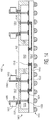
FIG. 1 through FIG. 4 illustrate, in a simplified cross-sectional view, an example semiconductor device with waveguide along line A-A ofFIG. 5 at stages of manufacture in accordance with an embodiment. -
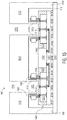
FIG. 5 illustrates, in a plan view, the example semiconductor device with waveguide at the stage of manufacture depicted inFIG. 4 in accordance with an embodiment. -
FIG. 6 andFIG. 7 illustrate, in a simplified cross-sectional view, an alternative example semiconductor device with waveguide along line B-B ofFIG. 8 at stages of manufacture in accordance with an embodiment. -
FIG. 8 illustrates, in a plan view, the example semiconductor device with waveguide at the stage of manufacture depicted inFIG. 7 in accordance with an embodiment. -
FIG. 9 through FIG. 11 illustrate, in a simplified cross-sectional view, an alternative example semiconductor device with waveguide along line C-C ofFIG. 12 at stages of manufacture in accordance with an embodiment. -
FIG. 12 illustrates, in a plan view, the example semiconductor device with waveguide at the stage of manufacture depicted inFIG. 11 in accordance with an embodiment. -
FIG. 13 through FIG. 15 illustrate, in a simplified cross-sectional view, an alternative example semiconductor device with waveguide along line D-D ofFIG. 16 at stages of manufacture in accordance with an embodiment. -
FIG. 16 illustrates, in a plan view, the example semiconductor device with waveguide at the stage of manufacture depicted inFIG. 15 in accordance with an embodiment. - Generally, there is provided, a semiconductor device including a packaged assembly with overlapping waveguide structure affixed to a common substrate. The waveguide structure is physically decoupled from the packaged assembly. A semiconductor die and launcher structure are encapsulated on a package substrate to form the packaged assembly. The waveguide structure includes a waveguide opening over an antenna launcher of the launcher structure allowing propagation of radio frequency (RF) signals. By having the overlapping waveguide structure physically decoupled from the packaged assembly, package stress is reduced and reliability is improved while providing low loss RF signal performance in a compact footprint.
-
FIG. 1 illustrates, in a simplified cross-sectional view, an example assembly of an example semiconductor device withwaveguide 100 along line A-A ofFIG. 5 at a stage of manufacture in accordance with an embodiment. At this stage of manufacture, the assembly ofsemiconductor device 100 includes asemiconductor die 102 andlauncher structures carrier substrate 104. - In this embodiment, the
launcher structures cavities 112 and 114). For example,launcher structure 106 includesconductive layers 122 and 130 (e.g., metal or other conductive material layers) separated by a non-conductive material 120 (e.g., FR-4, ceramic).Contacts 124 andvias 126 provide conductive connections betweenterminal pads 132 at a bottom surface oflauncher structure 106 andconductive layers cavity 112 includes anantenna launcher 116 located at a bottom surface of thecavity 112. Likewise, thecavity 114 includes anantenna launcher 118 located at a bottom surface of thecavity 114. Theantenna launcher 116 is connected toterminal pad 134 at the bottom surface oflauncher structure 106 by way of interconnecting contacts and via (e.g.,contacts 124, via 126). Viaplugs 128 may be incorporated invias 126 to provide additional strength and rigidity. In this embodiment,conductive layers 122 and interconnectingcontacts 124 are configured and arranged to serve as a conductive wall or fence substantially surrounding theantenna launcher 116. In some embodiments, it may be desirable to connect the conductive wall or fence to a ground supply terminal or other supply terminal. In this embodiment,conductive layer 130 is configured and arranged to serve as a signal reflector located below theantenna launcher 116 and substantially surrounding the via interconnecting theantenna launcher 116 with theterminal pad 134. In some embodiments, it may be desirable to form the signal reflector on a next conductive layer immediately below theantenna launcher 116. - The
semiconductor die 102 has an active surface (e.g., major surface having circuitry) and a backside surface (e.g., major surface opposite of the active surface). The semiconductor die 102 includesbond pads 110 at the active surface configured for connection toantenna launchers -
FIG. 2 illustrates, in a simplified cross-sectional view, the example assembly at a subsequent stage of manufacture in accordance with an embodiment. At this stage of manufacture, the assembly ofsemiconductor device 100 includes an encapsulant (e.g., epoxy material) 204 at least partially encapsulating semiconductor die 102 andlauncher structures carrier substrate 104. In this embodiment, the semiconductor die 102 andlauncher structures FAM tool 202 is in contact with a top surface of thelauncher structures cavities 112 and 114) clear of encapsulant (e.g., not encapsulated). -
FIG. 3 illustrates, in a simplified cross-sectional view, the example assembly at a subsequent stage of manufacture in accordance with an embodiment. At this stage of manufacture, theassembly 302 includes anencapsulant 204 at least partially encapsulating semiconductor die 102 andlauncher structures RDL substrate 304 andball connectors 310. After thecarrier substrate 104 is removed, theRDL substrate 304 is applied to the resulting exposed bottom surface including an exposed active surface of thesemiconductor die 102 and exposed bottom surfaces of thelauncher structures Conductive feeds RDL substrate 304 betweenbond pads 110 andterminal pads 134 to interconnect semiconductor die 102 andantenna launchers RDL substrate 304 is applied, conductive ball connectors 310 (e.g., solder balls) are affixed to a bottom surface of theRDL substrate 304. Theball connectors 310 are configured and arranged to provide conductive connections between theassembly 302 and a printed circuit board (PCB), for example.Ball connectors 310 may be any suitable conductive structure such as solder ball, gold studs, copper pillars, and the like, to connect conductive features of theassembly 302 with the PCB. In this embodiment, theRDL substrate 304 is formed as a build-up substrate including a redistribution layer. In some embodiments, theRDL substrate 304 may be formed as a pre-formed substrate including a redistribution layer. In other embodiments,ball connectors 310 may be directly affixed toterminal pads bond pads 110 to provide connectivity with a PCB, for example, without utilizing an RDL substrate. -
FIG. 4 illustrates, in a simplified cross-sectional view, the example semiconductor device withwaveguide 100 along line A-A ofFIG. 5 at a stage of manufacture in accordance with an embodiment. At this stage of manufacture, thesemiconductor device 100 includes theassembly 302 and overlappingwaveguide structure 402 affixed to acommon substrate 404. With theassembly 302 and overlappingwaveguide structure 402 affixed to thesubstrate 404, thewaveguide structure 402 is physically decoupled from theassembly 302. For example, thewaveguide structure 402 does not physically contact theassembly 302. In this embodiment,substrate 404 may be characterized as a PCB or other multilayer substrate configured to provide connectivity with other components of a system, for example. - The
waveguide structure 402 includes waveguides 406 (e.g., waveguide openings) and is attached to thesubstrate 404 atinterface surfaces 408. Thewaveguide structure 402 may be attached to thesubstrate 404 atinterface surfaces 408 using screws, alignment pins, adhesives, and combinations thereof, for example. In this embodiment, thewaveguide structure 402 is formed from a conductive material such as a metal (e.g., aluminum, copper), non-conductive material coated with conductive material, other conductive materials, or combinations thereof.Waveguides 406 are formed as waveguide openings in thewaveguide structure 402 withantenna launchers waveguide openings 406 includesidewall portions 410 which extend downward into thecavities antenna launchers Waveguides 406 dimensions (e.g., width, length) may be configured for propagation of signals (e.g., radar, mmWave signals, 30 GHz to 300 GHz) having desired wavelengths. For example, a waveguide may be configured for propagation (e.g., transmission) of a radar signal having a frequency of 77 GHz. Because a 77 GHz signal has a wavelength of approximately 4 mm, the waveguide is configured having a width dimension of approximately 2 mm, or half of the desired wavelength. -
FIG. 5 illustrates, in a plan view, the example semiconductor device withwaveguide 100 at the stage of manufacture depicted inFIG. 4 in accordance with an embodiment. At this stage of manufacture, thesemiconductor device 100 includes the assembly (302) and overlappingwaveguide structure 402 affixed to a common substrate (404). Underlying semiconductor die 102 is shown as dashed outline labeled 102 for reference. Cross-sectional views ofsemiconductor device 100 taken along lineA-A including waveguides 406 are shown in example stages of manufacture depicted inFIG. 1 through FIG. 4 .Waveguides 406 are formed as waveguide openings in thewaveguide structure 402 withantenna launchers non-conductive material 120 oflauncher structures -
FIG. 6 illustrates, in a simplified cross-sectional view, an example assembly of an example semiconductor device withwaveguide 200 along line B-B ofFIG. 8 at a stage of manufacture in accordance with an embodiment. At this stage of manufacture, theassembly 600 includes anencapsulant 638 at least partially encapsulating semiconductor die 602 andlauncher structures RDL substrate 604 andball connectors 644. Conductive feeds 640 and 642 are formed in theRDL substrate 604 betweenbond pads 610 andterminal pads 634 to interconnect semiconductor die 602 andantenna launchers RDL substrate 604. Theball connectors 644 are configured and arranged to provide conductive connections between theassembly 600 and a PCB, for example.Ball connectors 644 may be any suitable conductive structure such as solder balls, gold studs, copper pillars, and the like, to connect conductive features of theassembly 600 with the PCB. In this embodiment, theRDL substrate 604 is formed as a build-up substrate including a redistribution layer. In some embodiments, theRDL substrate 604 may be formed as a pre-formed substrate including a redistribution layer. In other embodiments,ball connectors 644 may be directly affixed to terminal pads 632-634 andbond pads 610 to provide connectivity with a PCB, for example, without utilizing an RDL substrate. - In this embodiment, the
launcher structures cavities 612 and 614). For example,launcher structure 606 includes conductive layers 622 (e.g., metal or other conductive material layers) separated by a non-conductive material 620 (e.g., FR-4, ceramic).Contacts 624 and vias 625 provide conductive connections betweenterminal pads 632 at a bottom surface oflauncher structure 606 andconductive layers 622. Thecavity 612 includes anantenna launcher 616 and surroundingconductive pad 630 located at a bottom surface of thecavity 612. Likewise, thecavity 614 includes anantenna launcher 618 and surrounding conductive pad located at a bottom surface of thecavity 614. Aconductive ring 626 is attached to theconductive pad 630 by way of a conductive connector 628 (e.g., solder, electrically conductive adhesive, anisotropic conductive film). Achannel 636 is formed in thecavity 612 between outer sidewall of theconductive ring 626 and sidewall ofcavity 612. Theantenna launcher 616 is connected toterminal pad 634 at the bottom surface oflauncher structure 606 by way of interconnecting contacts and via. In this embodiment,conductive layers 622 and interconnectingcontacts 624 are configured and arranged to serve as a conductive wall or fence substantially surrounding the sidewall ofcavity 612. In some embodiments, it may be desirable to connect the conductive wall or fence to a ground supply terminal or other supply terminal. - The semiconductor die 602 has an active surface (e.g., major surface having circuitry) and a backside surface (e.g., major surface opposite of the active surface). The semiconductor die 602 includes
bond pads 610 at the active surface configured for connection toantenna launchers -
FIG. 7 illustrates, in a simplified cross-sectional view, theexample semiconductor device 200 along line B-B ofFIG. 8 at a stage of manufacture in accordance with an embodiment. At this stage of manufacture, thesemiconductor device 200 includes theassembly 600 and overlappingwaveguide structure 702 affixed to acommon substrate 704. With theassembly 600 and overlappingwaveguide structure 702 affixed to thesubstrate 704, thewaveguide structure 702 is physically decoupled from theassembly 600. For example, thewaveguide structure 702 does not physically contact theassembly 600. In this embodiment,substrate 704 may be characterized as a PCB or other multilayer substrate configured to provide connectivity with other components of a system, for example. - The
waveguide structure 702 includes waveguides 706 (e.g., waveguide openings) and is attached to thesubstrate 704 at interface surfaces 708. Thewaveguide structure 702 may be attached to thesubstrate 704 atinterface surfaces 708 using screws, alignment pins, adhesives, and combinations thereof, for example. In this embodiment, thewaveguide structure 702 is formed from a conductive material such as a metal (e.g., aluminum, copper), other conductive materials, or combinations thereof.Waveguides 706 are formed as waveguide openings in thewaveguide structure 702 withantenna launchers waveguide openings 706 includesidewall portions 710 which extend downward into thechannels 636 formed in thecavities conductive rings 626 and sidewall ofcavities Waveguides 706 dimensions (e.g., width, length) may be configured for propagation of signals (e.g., radar, mmWave signals, 30 GHz to 300 GHz) having desired wavelengths. -
FIG. 8 illustrates, in a plan view, the example semiconductor device withwaveguide 200 at the stage of manufacture depicted inFIG. 7 in accordance with an embodiment. At this stage of manufacture, thesemiconductor device 200 includes the assembly (600) and overlappingwaveguide structure 702 affixed to a common substrate (704). Underlying semiconductor die 602 is shown as dashed outline labeled 602 for reference. Cross-sectional views of semiconductor device withwaveguide 200 taken along lineB-B including waveguides 706 are shown in example stages of manufacture depicted inFIG. 7 andFIG. 8 .Waveguides 706 are formed as waveguide openings in thewaveguide structure 702 withantenna launchers conductive rings 626, andnon-conductive material 620 oflauncher structures -
FIG. 9 illustrates, in a simplified cross-sectional view, an example assembly of an example semiconductor device withwaveguide 300 along line C-C ofFIG. 12 at a stage of manufacture in accordance with an embodiment. At this stage of manufacture, the assembly ofsemiconductor device 300 includes an encapsulant (e.g., epoxy material) 928 encapsulating semiconductor die 902 andlauncher structures carrier substrate 904. In this embodiment, the semiconductor die 902 andlauncher structures - In this embodiment, the
launcher structures antenna launcher launcher structures launcher structure 906 includesconductive interconnects 918 and 920 (e.g., metal or other conductive materials) separated by a non-conductive material 912 (e.g., FR-4, ceramic).Conductive interconnect 918 provides conductive connections betweenterminal pads 922 at a bottom surface oflauncher structure 906 and conductive ball connectors 926 (e.g., solder balls). Theantenna launcher 914 is connected toterminal pad 924 at the bottom surface oflauncher structure 906 by way of conductive interconnect 920.Conductive interconnect 918 andconductive ball connectors 926 are configured and arranged to substantially surroundantennal launcher 914 and conductive interconnect 920. - The semiconductor die 902 has an active surface (e.g., major surface having circuitry) and a backside surface (e.g., major surface opposite of the active surface). The semiconductor die 902 includes
bond pads 910 at the active surface configured for connection toantenna launchers -
FIG. 10 illustrates, in a simplified cross-sectional view, the example assembly at a subsequent stage of manufacture in accordance with an embodiment. At this stage of manufacture, theassembly 1000 includes theencapsulant 928 at least partially encapsulating semiconductor die 902 andlauncher structures RDL substrate 1004 andball connectors 1016. - In this embodiment, a backside grind operation is performed on the
assembly 1000 to expose portions ofball connectors 926 oflauncher structures conductive ring 1008 is attached to a conductive path formed by the exposed a portions ofball connectors 926 by way of a conductive connector 1006 (e.g., solder, electrically conductive adhesive, anisotropic conductive film). Theconductive ring 1008 is configured and arranged to serve as a conductive wall or fence substantially surrounding theantenna launcher 914 and forming acavity 1010. Likewise, a conductive ring substantially surrounds theantenna launcher 916 and forms acavity 1012. In some embodiments, it may be desirable to connect the conductive walls or fences to a ground supply terminal or other supply terminal. - After the
carrier substrate 904 is removed, theRDL substrate 1004 is applied to the resulting exposed bottom surface including an exposed active surface of the semiconductor die 902 and exposed bottom surfaces of thelauncher structures RDL substrate 1004 betweenbond pads 910 andterminal pads 924 to interconnect semiconductor die 902 andantenna launchers RDL substrate 1004 is applied, conductive ball connectors 1016 (e.g., solder balls) are affixed to a bottom surface of theRDL substrate 1004. Theball connectors 1016 are configured and arranged to provide conductive connections between theassembly 1000 and a printed circuit board (PCB), for example.Ball connectors 1016 may be any suitable conductive structure such as solder ball, gold studs, copper pillars, and the like, to connect conductive features of theassembly 1000 with the PCB. In this embodiment, theRDL substrate 1004 is formed as a build-up substrate including a redistribution layer. In some embodiments, theRDL substrate 1004 may be formed as a pre-formed substrate including a redistribution layer. In other embodiments,ball connectors 1016 may be directly affixed toterminal pads bond pads 910 to provide connectivity with a PCB, for example, without utilizing an RDL substrate. -
FIG. 11 illustrates, in a simplified cross-sectional view, the example semiconductor device withwaveguide 300 along line C-C ofFIG. 12 at a stage of manufacture in accordance with an embodiment. At this stage of manufacture, the semiconductor device withwaveguide 300 includes theassembly 1000 and overlappingwaveguide structure 1102 affixed to acommon substrate 1104. With theassembly 1000 and overlappingwaveguide structure 1102 affixed to thesubstrate 1104, thewaveguide structure 1102 is physically decoupled from theassembly 1000. For example, thewaveguide structure 1102 does not physically contact theassembly 1000. In this embodiment,substrate 1104 may be characterized as a PCB or other multilayer substrate configured to provide connectivity with other components of a system, for example. - The
waveguide structure 1102 includes waveguides 1106 (e.g., waveguide openings) and is attached to thesubstrate 1104 at interface surfaces 1108. Thewaveguide structure 1102 may be attached to thesubstrate 1104 atinterface surfaces 1108 using screws, alignment pins, adhesives, and combinations thereof, for example. In this embodiment, thewaveguide structure 1102 is formed from a conductive material such as a metal (e.g., aluminum, copper), other conductive materials, or combinations thereof.Waveguides 1106 are formed as waveguide openings in thewaveguide structure 1102 withconductive rings 1008 and a surface ofencapsulant 928 overantenna launchers waveguide openings 1106 are configured and arranged to substantially surround the conductive rings substantially surroundingantenna launchers waveguide 1106 include sidewalls 1110 which surround outer sidewalls of theconductive ring 1008.Waveguides 1106 dimensions (e.g., width, length) may be configured for propagation of signals (e.g., radar, mmWave signals, 30 GHz to 300 GHz) having desired wavelengths. -
FIG. 12 illustrates, in a plan view, the example semiconductor device withwaveguide 300 at the stage of manufacture depicted inFIG. 11 in accordance with an embodiment. At this stage of manufacture, thesemiconductor device 300 includes the assembly (1000) and overlappingwaveguide structure 1102 affixed to a common substrate (1104). Underlying semiconductor die 902 is shown as dashed outline labeled 902 for reference. Cross-sectional views ofsemiconductor device 300 taken along lineC-C including waveguides 1106 are shown in example stages of manufacture depicted inFIG. 9 through FIG. 11 .Waveguides 1106 are formed as waveguide openings in thewaveguide structure 1102 withconductive rings 1008 and encapsulant 928 over antenna launchers (914 and 916) exposed through the respective openings. -
FIG. 13 illustrates, in a simplified cross-sectional view, an example assembly of an example semiconductor device withwaveguide 400 along line D-D ofFIG. 16 at a stage of manufacture in accordance with an embodiment. At this stage of manufacture, the assembly ofsemiconductor device 400 includes an encapsulant (e.g., epoxy material) 1328 encapsulatingsemiconductor die 1302 andlauncher structures carrier substrate 1304. In this embodiment, the semiconductor die 1302 andlauncher structures - In this embodiment, the
launcher structures antenna launcher launcher structures launcher structure 1306 includesconductive interconnects 1318 and 1320 (e.g., metal or other conductive materials) separated by a non-conductive material 1312 (e.g., FR-4, ceramic).Conductive interconnect 1318 provides conductive connections betweenterminal pads 1322 at a bottom surface oflauncher structure 1306 and conductive ball connectors 1326 (e.g., solder balls). Theantenna launcher 1314 is connected toterminal pad 1324 at the bottom surface oflauncher structure 1306 by way ofconductive interconnect 1320.Conductive interconnect 1318 andconductive ball connectors 1326 are configured and arranged to substantially surroundantennal launcher 1314 andconductive interconnect 1320. - The semiconductor die 1302 has an active surface (e.g., major surface having circuitry) and a backside surface (e.g., major surface opposite of the active surface). The semiconductor die 1302 includes
bond pads 1310 at the active surface configured for connection toantenna launchers -
FIG. 14 illustrates, in a simplified cross-sectional view, the example assembly at a subsequent stage of manufacture in accordance with an embodiment. At this stage of manufacture, theassembly 1400 includes theencapsulant 1328 at least partially encapsulatingsemiconductor die 1302 andlauncher structures RDL substrate 1404 andball connectors 1418. - In this embodiment, a backside grind operation is performed on the
assembly 1400 to expose portions ofball connectors 1326launcher structures conductive ring 1408 is formed as a conductive layer (e.g., metal or other conductive material) on sidewalls of an opening in anon-conductive substrate 1410. Theconductive ring 1408 is attached to the exposed a portions ofball connectors 1326 by way of a conductive connector 1406 (e.g., solder, electrically conductive adhesive, anisotropic conductive film). Theconductive ring 1408 is configured and arranged to serve as a conductive wall or fence substantially surrounding theantenna launcher 1314 and forming acavity 1412. Likewise, a conductive ring substantially surrounds theantenna launcher 1316 and forms acavity 1414. In some embodiments, it may be desirable to connect the conductive walls or fences to a ground supply terminal or other supply terminal. - After the
carrier substrate 1304 is removed, theRDL substrate 1404 is applied to the resulting exposed bottom surface including an exposed active surface of the semiconductor die 1302 and exposed bottom surfaces of thelauncher structures RDL substrate 1404 betweenbond pads 1310 andterminal pads 1324 to interconnect semiconductor die 1302 andantenna launchers RDL substrate 1404 is applied, conductive ball connectors 1418 (e.g., solder balls) are affixed to a bottom surface of theRDL substrate 1404. Theball connectors 1418 are configured and arranged to provide conductive connections between theassembly 1400 and a printed circuit board (PCB), for example.Ball connectors 1418 may be any suitable conductive structure such as solder ball, gold studs, copper pillars, and the like, to connect conductive features of theassembly 1400 with the PCB. In this embodiment, theRDL substrate 1404 is formed as a build-up substrate including a redistribution layer. In some embodiments, theRDL substrate 1404 may be formed as a pre-formed substrate including a redistribution layer. In other embodiments,ball connectors 1418 may be directly affixed toterminal pads bond pads 1310 to provide connectivity with a PCB, for example, without utilizing an RDL substrate. -
FIG. 15 illustrates, in a simplified cross-sectional view, the example semiconductor device withwaveguide 400 along line D-D ofFIG. 16 at a stage of manufacture in accordance with an embodiment. At this stage of manufacture, the semiconductor device withwaveguide 400 includes theassembly 1400 and overlappingwaveguide structure 1502 affixed to acommon substrate 1504. With theassembly 1400 and overlappingwaveguide structure 1502 affixed to thesubstrate 1504, thewaveguide structure 1502 is physically decoupled from theassembly 1400. For example, thewaveguide structure 1502 does not physically contact theassembly 1400. In this embodiment,substrate 1504 may be characterized as a PCB or other multilayer substrate configured to provide connectivity with other components of a system, for example. - The
waveguide structure 1502 includes waveguides 1506 (e.g., waveguide openings) and is attached to thesubstrate 1504 at interface surfaces 1508. Thewaveguide structure 1502 may be attached to thesubstrate 1504 atinterface surfaces 1508 using screws, alignment pins, adhesives, and combinations thereof, for example. In this embodiment, thewaveguide structure 1502 is formed from a conductive material such as a metal (e.g., aluminum, copper), other conductive materials, or combinations thereof.Waveguides 1506 are formed as waveguide openings in thewaveguide structure 1502 with a surface ofencapsulant 1328 overantenna launchers waveguide openings 1506 includesidewall portions 1510 which extend downward into thecavities antenna launchers Waveguides 1506 dimensions (e.g., width, length) may be configured for propagation of signals (e.g., radar, mmWave signals, 30 GHz to 300 GHz) having desired wavelengths. -
FIG. 16 illustrates, in a plan view, the example semiconductor device withwaveguide 400 at the stage of manufacture depicted inFIG. 15 in accordance with an embodiment. At this stage of manufacture, the semiconductor device withwaveguide 400 includes the assembly (1400) and overlappingwaveguide structure 1502 affixed to a common substrate (1404). Underlying semiconductor die 1302 is shown as dashed outline labeled 1302 for reference. Cross-sectional views of semiconductor device withwaveguide 400 taken along lineD-D including waveguides 1506 are shown in example stages of manufacture depicted inFIG. 13 through FIG. 15 .Waveguides 1506 are formed as waveguide openings in thewaveguide structure 1502 withencapsulant 1328 over antenna launchers (1314 and 1316) exposed through the respective openings. - Generally, there is provided, a method of manufacturing a manufacturing a semiconductor device, the method including forming an assembly including placing a semiconductor die and a launcher structure on a carrier substrate, the launcher structure including an antenna launcher; encapsulating at least a portion of the semiconductor die and the launcher structure; applying a redistribution layer on a first major surface of the semiconductor die and a first major surface of the launcher structure, a bond pad of the semiconductor die connected by way of the redistribution layer to the antenna launcher; attaching the assembly to a substrate; and attaching a waveguide structure to the substrate, the waveguide structure overlapping the assembly and physically decoupled from the assembly. The launcher structure may be formed having a cavity, the antenna launcher located at a bottom surface of the cavity. The attaching the waveguide structure to the substrate may further include extending sidewalls of an opening in the waveguide structure into the cavity to substantially surround the antenna launcher. The dimensions of the opening in the waveguide structure may be configured for propagation of a mmWave signal. The method may further include forming a conductive ring structure substantially surround the antenna launcher, outer sidewalls of the conductive ring structure spaced from sidewalls of the cavity to form a channel between the conductive ring structure and sidewalls of the cavity. The attaching the waveguide structure to the substrate may further include extending sidewalls of an opening in the waveguide structure into the channel formed between the conductive ring structure and the sidewalls of the cavity. The method may further include back-grinding the assembly to expose a conductive path substantially surrounding the antenna launcher; and attaching a conductive ring structure onto the exposed conductive path. The attaching the waveguide structure to the substrate may further include extending sidewalls of an opening in the waveguide structure to substantially surround the conductive ring structure. The attaching the waveguide structure to the substrate may further include extending sidewalls of an opening in the waveguide structure to substantially surround the antenna launcher, the conductive ring structure surrounding the extended sidewall of the opening.
- In another embodiment, there is provided, a semiconductor device including a printed circuit board (PCB) having a topside surface; a packaged assembly attached to the PCB at the topside surface, the packaged assembly including a package substrate having a first major surface and a second major surface; a semiconductor die having an active surface and a backside surface, the semiconductor die attached to the package substrate at the first major surface; a launcher structure attached to the package substrate at the first major surface, the launcher structure including an antenna launcher coupled to the semiconductor die by way of the package substrate; and an epoxy material encapsulating at least a portion of the semiconductor die and the launcher structure; and a waveguide structure attached to the PCB at the topside surface, the waveguide structure overlapping the packaged assembly and physically decoupled from the packaged assembly. The package substrate may be characterized as a build-up substrate including a redistribution layer configured to couple a bond pad on the active surface of the semiconductor die with the antenna launcher. The waveguide structure may be configured and arranged for propagation of a mmWave signal. The launcher structure may be formed having a cavity, the antenna launcher located at a bottom surface of the cavity. The waveguide structure may include a waveguide opening having sidewall portions extended into the cavity and substantially surrounding the antenna launcher. The launcher structure may further include a conductive ring structure substantially surrounding the antenna launcher, outer sidewalls of the conductive ring structure spaced from sidewalls of the cavity to form a channel between the conductive ring structure and sidewalls of the cavity. The waveguide structure may include a waveguide opening having sidewall portions extended into the channel formed between the conductive ring structure and the sidewalls of the cavity.
- In yet another embodiment, there is provided, a semiconductor device including a printed circuit board (PCB) having a topside surface; a packaged semiconductor device attached to the PCB at the topside surface, the packaged semiconductor device including a package substrate having a first major surface and a second major surface; a semiconductor die having an active surface and a backside surface, the semiconductor die attached to the package substrate at the first major surface; a launcher structure attached to the package substrate at the first major surface, the launcher structure including an antenna launcher coupled to the semiconductor die by way a conductive feed of the package substrate; and an epoxy material encapsulating at least a portion of the semiconductor die and the launcher structure; and a waveguide structure attached to the PCB at the topside surface, the waveguide structure overlapping the packaged semiconductor device, a waveguide opening of the waveguide structure having sidewalls substantially surrounding the antenna launcher, the waveguide structure physically decoupled from the packaged semiconductor device. The launcher structure may be formed having a cavity, the antenna launcher located at a bottom surface of the cavity. The sidewall portions of the waveguide opening may extend into the cavity and substantially surround the antenna launcher. The launcher structure may further include a conductive ring structure substantially surrounding the antenna launcher and spaced from sidewalls of the cavity to form a channel between the conductive ring structure and sidewalls of the cavity, sidewall portions of the waveguide opening extend into the channel formed between the conductive ring structure and the sidewalls of the cavity.
- By now, it should be appreciated that there has been provided a semiconductor device including a packaged assembly with overlapping waveguide structure affixed to a common substrate. The waveguide structure is physically decoupled from the packaged assembly. A semiconductor die and launcher structure are encapsulated on a package substrate to form the packaged assembly. The waveguide structure includes a waveguide opening over an antenna launcher of the launcher structure allowing propagation of radio frequency (RF) signals. By having the overlapping waveguide structure physically decoupled from the packaged assembly, package stress is reduced and reliability is improved while providing low loss RF signal performance in a compact footprint. Further, a method of manufacturing a semiconductor device is provided. The method includes forming an assembly including placing a semiconductor die and a launcher structure on a carrier substrate, encapsulating at least a portion of the semiconductor die and the launcher structure, and applying a redistribution layer on a surface of the semiconductor die and a surface of the launcher structure to connect a bond pad of the semiconductor die with an antenna launcher of the launcher structure. The assembly is attached to a substrate and a waveguide overlapping the assembly is attached to the substrate. The waveguide structure is physically decoupled from the assembly.
- The terms "front," "back," "top," "bottom," "over," "under" and the like in the description and in the claims, if any, are used for descriptive purposes and not necessarily for describing permanent relative positions. It is understood that the terms so used are interchangeable under appropriate circumstances such that the embodiments of the invention described herein are, for example, capable of operation in other orientations than those illustrated or otherwise described herein.
- Although the invention is described herein with reference to specific embodiments, various modifications and changes can be made without departing from the scope of the present invention as set forth in the claims below. Accordingly, the specification and figures are to be regarded in an illustrative rather than a restrictive sense, and all such modifications are intended to be included within the scope of the present invention. Any benefits, advantages, or solutions to problems that are described herein with regard to specific embodiments are not intended to be construed as a critical, required, or essential feature or element of any or all the claims.
- Furthermore, the terms "a" or "an," as used herein, are defined as one or more than one. Also, the use of introductory phrases such as "at least one" and "one or more" in the claims should not be construed to imply that the introduction of another claim element by the indefinite articles "a" or "an" limits any particular claim containing such introduced claim element to inventions containing only one such element, even when the same claim includes the introductory phrases "one or more" or "at least one" and indefinite articles such as "a" or "an." The same holds true for the use of definite articles.
- Unless stated otherwise, terms such as "first" and "second" are used to arbitrarily distinguish between the elements such terms describe. Thus, these terms are not necessarily intended to indicate temporal or other prioritization of such elements.
Claims (15)
- A method of manufacturing a semiconductor device, the method comprising:forming an assembly comprising:placing a semiconductor die and a launcher structure on a carrier substrate, the launcher structure including an antenna launcher;encapsulating at least a portion of the semiconductor die and the launcher structure;applying a redistribution layer on a first major surface of the semiconductor die and a first major surface of the launcher structure, a bond pad of the semiconductor die connected by way of the redistribution layer to the antenna launcher;attaching the assembly to a substrate; andattaching a waveguide structure to the substrate, the waveguide structure overlapping the assembly and physically decoupled from the assembly.
- The method of claim 1, wherein the launcher structure is formed having a cavity, the antenna launcher located at a bottom surface of the cavity.
- The method of claim 2, wherein attaching the waveguide structure to the substrate further includes extending sidewalls of an opening in the waveguide structure into the cavity to substantially surround the antenna launcher.
- The method of claim 3, wherein dimensions of the opening in the waveguide structure are configured for propagation of a mmWave signal.
- The method of any of claims 2 to 4, further comprising forming a conductive ring structure substantially surround the antenna launcher, outer sidewalls of the conductive ring structure spaced from sidewalls of the cavity to form a channel between the conductive ring structure and sidewalls of the cavity.
- The method of claim 5, wherein attaching the waveguide structure to the substrate further includes extending sidewalls of an opening in the waveguide structure into the channel formed between the conductive ring structure and the sidewalls of the cavity.
- The method of any preceding claim, further comprising:back-grinding the assembly to expose a conductive path substantially surrounding the antenna launcher; andattaching a conductive ring structure onto the exposed conductive path.
- The method of claim 7, wherein attaching the waveguide structure to the substrate further includes extending sidewalls of an opening in the waveguide structure to substantially surround the conductive ring structure.
- The method of claim 7 or 8, wherein attaching the waveguide structure to the substrate further includes extending sidewalls of an opening in the waveguide structure to substantially surround the antenna launcher, the conductive ring structure surrounding the extended sidewall of the opening.
- A semiconductor device comprising:a printed circuit board (PCB) having a topside surface;a packaged assembly attached to the PCB at the topside surface, the packaged assembly comprising:a package substrate having a first major surface and a second major surface;a semiconductor die having an active surface and a backside surface, the semiconductor die attached to the package substrate at the first major surface;a launcher structure attached to the package substrate at the first major surface, the launcher structure including an antenna launcher coupled to the semiconductor die by way of the package substrate; andan epoxy material encapsulating at least a portion of the semiconductor die and the launcher structure; anda waveguide structure attached to the PCB at the topside surface, the waveguide structure overlapping the packaged assembly and physically decoupled from the packaged assembly.
- The semiconductor device of claim 10, wherein the package substrate is characterized as a build-up substrate comprising a redistribution layer configured to couple a bond pad on the active surface of the semiconductor die with the antenna launcher.
- The semiconductor device of claim 10 or 11, wherein the waveguide structure is configured and arranged for propagation of a mmWave signal.
- The semiconductor device of any of claims 10 to 12, wherein the launcher structure is formed having a cavity, the antenna launcher located at a bottom surface of the cavity.
- The semiconductor device of claim 13, wherein the waveguide structure includes a waveguide opening having sidewall portions extended into the cavity and substantially surrounding the antenna launcher.
- The semiconductor device of claim 13 or 14, wherein the launcher structure further includes a conductive ring structure substantially surrounding the antenna launcher, outer sidewalls of the conductive ring structure spaced from sidewalls of the cavity to form a channel between the conductive ring structure and sidewalls of the cavity.
Applications Claiming Priority (1)
| Application Number | Priority Date | Filing Date | Title |
|---|---|---|---|
| US16/716,680 US11133273B2 (en) | 2019-12-17 | 2019-12-17 | Semiconductor device with waveguide and method therefor |
Publications (2)
| Publication Number | Publication Date |
|---|---|
| EP3840114A1 true EP3840114A1 (en) | 2021-06-23 |
| EP3840114B1 EP3840114B1 (en) | 2024-05-29 |
Family
ID=73740328
Family Applications (1)
| Application Number | Title | Priority Date | Filing Date |
|---|---|---|---|
| EP20212279.2A Active EP3840114B1 (en) | 2019-12-17 | 2020-12-07 | Semiconductor device with waveguide and method therefor |
Country Status (3)
| Country | Link |
|---|---|
| US (2) | US11133273B2 (en) |
| EP (1) | EP3840114B1 (en) |
| CN (1) | CN112992802A (en) |
Families Citing this family (13)
| Publication number | Priority date | Publication date | Assignee | Title |
|---|---|---|---|---|
| KR102815728B1 (en) * | 2020-06-22 | 2025-06-02 | 삼성전자주식회사 | Semiconductor package |
| US12126067B2 (en) | 2020-06-25 | 2024-10-22 | Intel Corporation | Millimeter-wave dielectric waveguide including an opening of varying cross-section enclosed within a first material and the first material surrounded by a second material |
| US11955684B2 (en) | 2020-06-25 | 2024-04-09 | Intel Corporation | Components for millimeter-wave communication |
| US12126068B2 (en) | 2020-06-25 | 2024-10-22 | Intel Corporation | Millimeter-wave dielectric waveguide bundle including first and second adjacent dielectric waveguides having different core and/or cladding materials |
| US12021289B2 (en) * | 2020-06-25 | 2024-06-25 | Intel Corporation | Components for millimeter-wave communication |
| US12166261B2 (en) | 2020-06-25 | 2024-12-10 | Intel Corporation | Components for millimeter-wave communication |
| US11355454B2 (en) * | 2020-07-30 | 2022-06-07 | Taiwan Semiconductor Manufacturing Company, Ltd. | Package structure and manufacturing method thereof |
| US11557544B2 (en) * | 2020-08-27 | 2023-01-17 | Nxp Usa, Inc. | Semiconductor device having a translation feature and method therefor |
| TWI796738B (en) * | 2021-07-23 | 2023-03-21 | 先豐通訊股份有限公司 | Circuit board structure having waveguide and method for manufacturing the same |
| US11735830B2 (en) * | 2021-08-06 | 2023-08-22 | Advanced Semiconductor Engineering, Inc. | Antenna device and method for manufacturing the same |
| US12288927B2 (en) * | 2021-10-25 | 2025-04-29 | Nxp Usa, Inc. | Semiconductor device with low loss waveguide interface and method therefor |
| US11961776B2 (en) * | 2021-11-30 | 2024-04-16 | Nxp Usa, Inc. | Semiconductor device with connector in package and method therefor |
| US20240145928A1 (en) * | 2022-10-28 | 2024-05-02 | Texas Instruments Incorporated | On-package signal launch and antenna structure |
Citations (6)
| Publication number | Priority date | Publication date | Assignee | Title |
|---|---|---|---|---|
| US20150229017A1 (en) * | 2014-02-07 | 2015-08-13 | Fujitsu Limited | High frequency module and fabrication method for high frequency module |
| US20160043455A1 (en) * | 2014-08-07 | 2016-02-11 | Infineon Technologies Ag | Microwave Chip Package Device |
| US20170324135A1 (en) * | 2014-12-12 | 2017-11-09 | Sony Corporation | Microwave antenna apparatus, packing and manufacturing method |
| US20190115643A1 (en) * | 2016-04-01 | 2019-04-18 | Sony Corporation | Microwave antenna apparatus, packing and manufacturing method |
| US20190348746A1 (en) * | 2018-05-14 | 2019-11-14 | Texas Instruments Incorporated | Wireless device with waveguiding structures between radiating structures and waveguide feeds |
| WO2020231905A1 (en) * | 2019-05-14 | 2020-11-19 | Texas Instruments Incorporated | Grounded bga wawe-guiding interface |
Family Cites Families (17)
| Publication number | Priority date | Publication date | Assignee | Title |
|---|---|---|---|---|
| DE102006007381A1 (en) * | 2006-02-15 | 2007-08-23 | Infineon Technologies Ag | Ultra-wide-band semiconductor component for ultra-wide-band standard in communication, comprises semiconductor component, ultra-wide-band semiconductor chip and multilevel circuit substrate with lower and upper metal layer |
| US9219041B2 (en) | 2012-03-29 | 2015-12-22 | International Business Machines Corporation | Electronic package for millimeter wave semiconductor dies |
| US9356352B2 (en) * | 2012-10-22 | 2016-05-31 | Texas Instruments Incorporated | Waveguide coupler |
| US9136230B2 (en) | 2013-03-28 | 2015-09-15 | Broadcom Corporation | IC package with integrated waveguide launcher |
| US9059490B2 (en) * | 2013-10-08 | 2015-06-16 | Blackberry Limited | 60 GHz integrated circuit to printed circuit board transitions |
| US10103447B2 (en) | 2014-06-13 | 2018-10-16 | Nxp Usa, Inc. | Integrated circuit package with radio frequency coupling structure |
| US9806040B2 (en) * | 2015-07-29 | 2017-10-31 | STATS ChipPAC Pte. Ltd. | Antenna in embedded wafer-level ball-grid array package |
| US9735118B2 (en) * | 2015-12-04 | 2017-08-15 | Taiwan Semiconductor Manufacturing Company, Ltd. | Antennas and waveguides in InFO structures |
| US10269702B2 (en) * | 2016-01-29 | 2019-04-23 | Taiwan Semiconductor Manufacturing Company, Ltd. | Info coil structure and methods of manufacturing same |
| US10460987B2 (en) * | 2017-05-09 | 2019-10-29 | Taiwan Semiconductor Manufacturing Company Ltd. | Semiconductor package device with integrated antenna and manufacturing method thereof |
| US10056922B1 (en) * | 2017-06-14 | 2018-08-21 | Infineon Technologies Ag | Radio frequency device modules and methods of formation thereof |
| DE102017123360A1 (en) * | 2017-10-09 | 2019-04-11 | Infineon Technologies Ag | METHOD FOR FORMING A SEMICONDUCTOR ASSEMBLY AND SEMICONDUCTOR ASSEMBLY |
| US10886590B2 (en) | 2017-10-11 | 2021-01-05 | Texas Instruments Incorporated | Interposer for connecting an antenna on an IC substrate to a dielectric waveguide through an interface waveguide located within an interposer block |
| US10833414B2 (en) * | 2018-03-02 | 2020-11-10 | Samsung Electro-Mechanics Co., Ltd. | Antenna apparatus and antenna module |
| US10651541B1 (en) * | 2019-02-27 | 2020-05-12 | Nxp Usa, Inc. | Package integrated waveguide |
| US11031681B2 (en) * | 2019-06-20 | 2021-06-08 | Nxp Usa, Inc. | Package integrated waveguide |
| US11508677B2 (en) * | 2019-08-29 | 2022-11-22 | Taiwan Semiconductor Manufacturing Company Ltd. | Semiconductor package for high-speed data transmission and manufacturing method thereof |
-
2019
- 2019-12-17 US US16/716,680 patent/US11133273B2/en active Active
-
2020
- 2020-12-07 EP EP20212279.2A patent/EP3840114B1/en active Active
- 2020-12-17 CN CN202011503662.2A patent/CN112992802A/en active Pending
-
2021
- 2021-08-26 US US17/412,687 patent/US11837560B2/en active Active
Patent Citations (6)
| Publication number | Priority date | Publication date | Assignee | Title |
|---|---|---|---|---|
| US20150229017A1 (en) * | 2014-02-07 | 2015-08-13 | Fujitsu Limited | High frequency module and fabrication method for high frequency module |
| US20160043455A1 (en) * | 2014-08-07 | 2016-02-11 | Infineon Technologies Ag | Microwave Chip Package Device |
| US20170324135A1 (en) * | 2014-12-12 | 2017-11-09 | Sony Corporation | Microwave antenna apparatus, packing and manufacturing method |
| US20190115643A1 (en) * | 2016-04-01 | 2019-04-18 | Sony Corporation | Microwave antenna apparatus, packing and manufacturing method |
| US20190348746A1 (en) * | 2018-05-14 | 2019-11-14 | Texas Instruments Incorporated | Wireless device with waveguiding structures between radiating structures and waveguide feeds |
| WO2020231905A1 (en) * | 2019-05-14 | 2020-11-19 | Texas Instruments Incorporated | Grounded bga wawe-guiding interface |
Also Published As
| Publication number | Publication date |
|---|---|
| US11837560B2 (en) | 2023-12-05 |
| US11133273B2 (en) | 2021-09-28 |
| EP3840114B1 (en) | 2024-05-29 |
| US20210391285A1 (en) | 2021-12-16 |
| CN112992802A (en) | 2021-06-18 |
| US20210183796A1 (en) | 2021-06-17 |
Similar Documents
| Publication | Publication Date | Title |
|---|---|---|
| US11837560B2 (en) | Semiconductor device with waveguide and method therefor | |
| US11031681B2 (en) | Package integrated waveguide | |
| US10651541B1 (en) | Package integrated waveguide | |
| US11664567B2 (en) | Hollow waveguide assembly formed by affixing first and second substrates to form a cavity therein and having a conductive layer covering the cavity | |
| US20190109103A1 (en) | Method of Forming a Semiconductor Package and Semiconductor Package | |
| EP4170819B1 (en) | Semiconductor device with low loss waveguide interface and method therefor | |
| EP4336550A1 (en) | Semiconductor device with through package via and method therefor | |
| US12288766B2 (en) | Semiconductor device with open cavity and method therefor | |
| US12588517B2 (en) | Semiconductor device with self-aligned waveguide and method therefor | |
| EP4195241A2 (en) | Semiconductor device with open cavity and manufacturing method thereof | |
| US11557544B2 (en) | Semiconductor device having a translation feature and method therefor | |
| EP4092829B1 (en) | Semiconductor device with directing structure and method therefor | |
| US11961776B2 (en) | Semiconductor device with connector in package and method therefor | |
| EP4550419A2 (en) | Package on package semiconductor device with integrated waveguide and method therefor | |
| US12406949B2 (en) | Semiconductor device with RF interposer and method therefor | |
| EP4648107A1 (en) | Package on package semiconductor device with integrated antenna and method therefor | |
| US12341089B2 (en) | Device package substrate structure and method therefor | |
| US20260060091A1 (en) | Semiconductor device with hybrid waveguide and method therefor | |
| CN119092469A (en) | System-level packaging structure and manufacturing method thereof |
Legal Events
| Date | Code | Title | Description |
|---|---|---|---|
| PUAI | Public reference made under article 153(3) epc to a published international application that has entered the european phase |
Free format text: ORIGINAL CODE: 0009012 |
|
| STAA | Information on the status of an ep patent application or granted ep patent |
Free format text: STATUS: THE APPLICATION HAS BEEN PUBLISHED |
|
| AK | Designated contracting states |
Kind code of ref document: A1 Designated state(s): AL AT BE BG CH CY CZ DE DK EE ES FI FR GB GR HR HU IE IS IT LI LT LU LV MC MK MT NL NO PL PT RO RS SE SI SK SM TR |
|
| STAA | Information on the status of an ep patent application or granted ep patent |
Free format text: STATUS: REQUEST FOR EXAMINATION WAS MADE |
|
| 17P | Request for examination filed |
Effective date: 20211223 |
|
| RBV | Designated contracting states (corrected) |
Designated state(s): AL AT BE BG CH CY CZ DE DK EE ES FI FR GB GR HR HU IE IS IT LI LT LU LV MC MK MT NL NO PL PT RO RS SE SI SK SM TR |
|
| STAA | Information on the status of an ep patent application or granted ep patent |
Free format text: STATUS: EXAMINATION IS IN PROGRESS |
|
| 17Q | First examination report despatched |
Effective date: 20221207 |
|
| GRAP | Despatch of communication of intention to grant a patent |
Free format text: ORIGINAL CODE: EPIDOSNIGR1 |
|
| STAA | Information on the status of an ep patent application or granted ep patent |
Free format text: STATUS: GRANT OF PATENT IS INTENDED |
|
| RIC1 | Information provided on ipc code assigned before grant |
Ipc: H01L 23/498 20060101ALN20240205BHEP Ipc: G01S 13/931 20200101ALN20240205BHEP Ipc: H01L 23/00 20060101ALI20240205BHEP Ipc: H01L 23/66 20060101ALI20240205BHEP Ipc: H01L 23/538 20060101ALI20240205BHEP Ipc: H01L 23/13 20060101ALI20240205BHEP Ipc: G01S 7/03 20060101ALI20240205BHEP Ipc: H01Q 21/00 20060101ALI20240205BHEP Ipc: H01Q 21/06 20060101ALI20240205BHEP Ipc: H01Q 13/06 20060101ALI20240205BHEP Ipc: H01Q 1/22 20060101AFI20240205BHEP |
|
| INTG | Intention to grant announced |
Effective date: 20240223 |
|
| GRAS | Grant fee paid |
Free format text: ORIGINAL CODE: EPIDOSNIGR3 |
|
| GRAA | (expected) grant |
Free format text: ORIGINAL CODE: 0009210 |
|
| STAA | Information on the status of an ep patent application or granted ep patent |
Free format text: STATUS: THE PATENT HAS BEEN GRANTED |
|
| AK | Designated contracting states |
Kind code of ref document: B1 Designated state(s): AL AT BE BG CH CY CZ DE DK EE ES FI FR GB GR HR HU IE IS IT LI LT LU LV MC MK MT NL NO PL PT RO RS SE SI SK SM TR |
|
| REG | Reference to a national code |
Ref country code: CH Ref legal event code: EP |
|
| REG | Reference to a national code |
Ref country code: IE Ref legal event code: FG4D |
|
| REG | Reference to a national code |
Ref country code: DE Ref legal event code: R096 Ref document number: 602020031589 Country of ref document: DE |
|
| REG | Reference to a national code |
Ref country code: LT Ref legal event code: MG9D |
|
| REG | Reference to a national code |
Ref country code: NL Ref legal event code: MP Effective date: 20240529 |
|
| PG25 | Lapsed in a contracting state [announced via postgrant information from national office to epo] |
Ref country code: IS Free format text: LAPSE BECAUSE OF FAILURE TO SUBMIT A TRANSLATION OF THE DESCRIPTION OR TO PAY THE FEE WITHIN THE PRESCRIBED TIME-LIMIT Effective date: 20240929 |
|
| PG25 | Lapsed in a contracting state [announced via postgrant information from national office to epo] |
Ref country code: BG Free format text: LAPSE BECAUSE OF FAILURE TO SUBMIT A TRANSLATION OF THE DESCRIPTION OR TO PAY THE FEE WITHIN THE PRESCRIBED TIME-LIMIT Effective date: 20240529 |
|
| PG25 | Lapsed in a contracting state [announced via postgrant information from national office to epo] |
Ref country code: FI Free format text: LAPSE BECAUSE OF FAILURE TO SUBMIT A TRANSLATION OF THE DESCRIPTION OR TO PAY THE FEE WITHIN THE PRESCRIBED TIME-LIMIT Effective date: 20240529 Ref country code: HR Free format text: LAPSE BECAUSE OF FAILURE TO SUBMIT A TRANSLATION OF THE DESCRIPTION OR TO PAY THE FEE WITHIN THE PRESCRIBED TIME-LIMIT Effective date: 20240529 |
|
| PG25 | Lapsed in a contracting state [announced via postgrant information from national office to epo] |
Ref country code: GR Free format text: LAPSE BECAUSE OF FAILURE TO SUBMIT A TRANSLATION OF THE DESCRIPTION OR TO PAY THE FEE WITHIN THE PRESCRIBED TIME-LIMIT Effective date: 20240830 |
|
| REG | Reference to a national code |
Ref country code: AT Ref legal event code: MK05 Ref document number: 1691425 Country of ref document: AT Kind code of ref document: T Effective date: 20240529 |
|
| PG25 | Lapsed in a contracting state [announced via postgrant information from national office to epo] |
Ref country code: ES Free format text: LAPSE BECAUSE OF FAILURE TO SUBMIT A TRANSLATION OF THE DESCRIPTION OR TO PAY THE FEE WITHIN THE PRESCRIBED TIME-LIMIT Effective date: 20240529 |
|
| PG25 | Lapsed in a contracting state [announced via postgrant information from national office to epo] |
Ref country code: AT Free format text: LAPSE BECAUSE OF FAILURE TO SUBMIT A TRANSLATION OF THE DESCRIPTION OR TO PAY THE FEE WITHIN THE PRESCRIBED TIME-LIMIT Effective date: 20240529 |
|
| PG25 | Lapsed in a contracting state [announced via postgrant information from national office to epo] |
Ref country code: PL Free format text: LAPSE BECAUSE OF FAILURE TO SUBMIT A TRANSLATION OF THE DESCRIPTION OR TO PAY THE FEE WITHIN THE PRESCRIBED TIME-LIMIT Effective date: 20240529 |
|
| PG25 | Lapsed in a contracting state [announced via postgrant information from national office to epo] |
Ref country code: LV Free format text: LAPSE BECAUSE OF FAILURE TO SUBMIT A TRANSLATION OF THE DESCRIPTION OR TO PAY THE FEE WITHIN THE PRESCRIBED TIME-LIMIT Effective date: 20240529 |
|
| PG25 | Lapsed in a contracting state [announced via postgrant information from national office to epo] |
Ref country code: PL Free format text: LAPSE BECAUSE OF FAILURE TO SUBMIT A TRANSLATION OF THE DESCRIPTION OR TO PAY THE FEE WITHIN THE PRESCRIBED TIME-LIMIT Effective date: 20240529 Ref country code: NO Free format text: LAPSE BECAUSE OF FAILURE TO SUBMIT A TRANSLATION OF THE DESCRIPTION OR TO PAY THE FEE WITHIN THE PRESCRIBED TIME-LIMIT Effective date: 20240829 Ref country code: LV Free format text: LAPSE BECAUSE OF FAILURE TO SUBMIT A TRANSLATION OF THE DESCRIPTION OR TO PAY THE FEE WITHIN THE PRESCRIBED TIME-LIMIT Effective date: 20240529 Ref country code: IS Free format text: LAPSE BECAUSE OF FAILURE TO SUBMIT A TRANSLATION OF THE DESCRIPTION OR TO PAY THE FEE WITHIN THE PRESCRIBED TIME-LIMIT Effective date: 20240929 Ref country code: HR Free format text: LAPSE BECAUSE OF FAILURE TO SUBMIT A TRANSLATION OF THE DESCRIPTION OR TO PAY THE FEE WITHIN THE PRESCRIBED TIME-LIMIT Effective date: 20240529 Ref country code: GR Free format text: LAPSE BECAUSE OF FAILURE TO SUBMIT A TRANSLATION OF THE DESCRIPTION OR TO PAY THE FEE WITHIN THE PRESCRIBED TIME-LIMIT Effective date: 20240830 Ref country code: FI Free format text: LAPSE BECAUSE OF FAILURE TO SUBMIT A TRANSLATION OF THE DESCRIPTION OR TO PAY THE FEE WITHIN THE PRESCRIBED TIME-LIMIT Effective date: 20240529 Ref country code: ES Free format text: LAPSE BECAUSE OF FAILURE TO SUBMIT A TRANSLATION OF THE DESCRIPTION OR TO PAY THE FEE WITHIN THE PRESCRIBED TIME-LIMIT Effective date: 20240529 Ref country code: BG Free format text: LAPSE BECAUSE OF FAILURE TO SUBMIT A TRANSLATION OF THE DESCRIPTION OR TO PAY THE FEE WITHIN THE PRESCRIBED TIME-LIMIT Effective date: 20240529 Ref country code: AT Free format text: LAPSE BECAUSE OF FAILURE TO SUBMIT A TRANSLATION OF THE DESCRIPTION OR TO PAY THE FEE WITHIN THE PRESCRIBED TIME-LIMIT Effective date: 20240529 Ref country code: RS Free format text: LAPSE BECAUSE OF FAILURE TO SUBMIT A TRANSLATION OF THE DESCRIPTION OR TO PAY THE FEE WITHIN THE PRESCRIBED TIME-LIMIT Effective date: 20240829 |
|
| PG25 | Lapsed in a contracting state [announced via postgrant information from national office to epo] |
Ref country code: NL Free format text: LAPSE BECAUSE OF FAILURE TO SUBMIT A TRANSLATION OF THE DESCRIPTION OR TO PAY THE FEE WITHIN THE PRESCRIBED TIME-LIMIT Effective date: 20240529 |
|
| PG25 | Lapsed in a contracting state [announced via postgrant information from national office to epo] |
Ref country code: NL Free format text: LAPSE BECAUSE OF FAILURE TO SUBMIT A TRANSLATION OF THE DESCRIPTION OR TO PAY THE FEE WITHIN THE PRESCRIBED TIME-LIMIT Effective date: 20240529 |
|
| PG25 | Lapsed in a contracting state [announced via postgrant information from national office to epo] |
Ref country code: DK Free format text: LAPSE BECAUSE OF FAILURE TO SUBMIT A TRANSLATION OF THE DESCRIPTION OR TO PAY THE FEE WITHIN THE PRESCRIBED TIME-LIMIT Effective date: 20240529 |
|
| PG25 | Lapsed in a contracting state [announced via postgrant information from national office to epo] |
Ref country code: EE Free format text: LAPSE BECAUSE OF FAILURE TO SUBMIT A TRANSLATION OF THE DESCRIPTION OR TO PAY THE FEE WITHIN THE PRESCRIBED TIME-LIMIT Effective date: 20240529 |
|
| PG25 | Lapsed in a contracting state [announced via postgrant information from national office to epo] |
Ref country code: CZ Free format text: LAPSE BECAUSE OF FAILURE TO SUBMIT A TRANSLATION OF THE DESCRIPTION OR TO PAY THE FEE WITHIN THE PRESCRIBED TIME-LIMIT Effective date: 20240529 |
|
| PG25 | Lapsed in a contracting state [announced via postgrant information from national office to epo] |
Ref country code: SK Free format text: LAPSE BECAUSE OF FAILURE TO SUBMIT A TRANSLATION OF THE DESCRIPTION OR TO PAY THE FEE WITHIN THE PRESCRIBED TIME-LIMIT Effective date: 20240529 Ref country code: RO Free format text: LAPSE BECAUSE OF FAILURE TO SUBMIT A TRANSLATION OF THE DESCRIPTION OR TO PAY THE FEE WITHIN THE PRESCRIBED TIME-LIMIT Effective date: 20240529 |
|
| PG25 | Lapsed in a contracting state [announced via postgrant information from national office to epo] |
Ref country code: SM Free format text: LAPSE BECAUSE OF FAILURE TO SUBMIT A TRANSLATION OF THE DESCRIPTION OR TO PAY THE FEE WITHIN THE PRESCRIBED TIME-LIMIT Effective date: 20240529 |
|
| PG25 | Lapsed in a contracting state [announced via postgrant information from national office to epo] |
Ref country code: SM Free format text: LAPSE BECAUSE OF FAILURE TO SUBMIT A TRANSLATION OF THE DESCRIPTION OR TO PAY THE FEE WITHIN THE PRESCRIBED TIME-LIMIT Effective date: 20240529 Ref country code: SK Free format text: LAPSE BECAUSE OF FAILURE TO SUBMIT A TRANSLATION OF THE DESCRIPTION OR TO PAY THE FEE WITHIN THE PRESCRIBED TIME-LIMIT Effective date: 20240529 Ref country code: RO Free format text: LAPSE BECAUSE OF FAILURE TO SUBMIT A TRANSLATION OF THE DESCRIPTION OR TO PAY THE FEE WITHIN THE PRESCRIBED TIME-LIMIT Effective date: 20240529 Ref country code: EE Free format text: LAPSE BECAUSE OF FAILURE TO SUBMIT A TRANSLATION OF THE DESCRIPTION OR TO PAY THE FEE WITHIN THE PRESCRIBED TIME-LIMIT Effective date: 20240529 Ref country code: DK Free format text: LAPSE BECAUSE OF FAILURE TO SUBMIT A TRANSLATION OF THE DESCRIPTION OR TO PAY THE FEE WITHIN THE PRESCRIBED TIME-LIMIT Effective date: 20240529 Ref country code: CZ Free format text: LAPSE BECAUSE OF FAILURE TO SUBMIT A TRANSLATION OF THE DESCRIPTION OR TO PAY THE FEE WITHIN THE PRESCRIBED TIME-LIMIT Effective date: 20240529 |
|
| PG25 | Lapsed in a contracting state [announced via postgrant information from national office to epo] |
Ref country code: IT Free format text: LAPSE BECAUSE OF FAILURE TO SUBMIT A TRANSLATION OF THE DESCRIPTION OR TO PAY THE FEE WITHIN THE PRESCRIBED TIME-LIMIT Effective date: 20240529 |
|
| REG | Reference to a national code |
Ref country code: DE Ref legal event code: R097 Ref document number: 602020031589 Country of ref document: DE |
|
| PLBE | No opposition filed within time limit |
Free format text: ORIGINAL CODE: 0009261 |
|
| STAA | Information on the status of an ep patent application or granted ep patent |
Free format text: STATUS: NO OPPOSITION FILED WITHIN TIME LIMIT |
|
| PG25 | Lapsed in a contracting state [announced via postgrant information from national office to epo] |
Ref country code: SI Free format text: LAPSE BECAUSE OF FAILURE TO SUBMIT A TRANSLATION OF THE DESCRIPTION OR TO PAY THE FEE WITHIN THE PRESCRIBED TIME-LIMIT Effective date: 20240529 |
|
| 26N | No opposition filed |
Effective date: 20250303 |
|
| PG25 | Lapsed in a contracting state [announced via postgrant information from national office to epo] |
Ref country code: MC Free format text: LAPSE BECAUSE OF FAILURE TO SUBMIT A TRANSLATION OF THE DESCRIPTION OR TO PAY THE FEE WITHIN THE PRESCRIBED TIME-LIMIT Effective date: 20240529 |
|
| P01 | Opt-out of the competence of the unified patent court (upc) registered |
Free format text: CASE NUMBER: APP_29897/2025 Effective date: 20250623 |
|
| REG | Reference to a national code |
Ref country code: CH Ref legal event code: PL |
|
| PG25 | Lapsed in a contracting state [announced via postgrant information from national office to epo] |
Ref country code: LU Free format text: LAPSE BECAUSE OF NON-PAYMENT OF DUE FEES Effective date: 20241207 |
|
| PG25 | Lapsed in a contracting state [announced via postgrant information from national office to epo] |
Ref country code: SE Free format text: LAPSE BECAUSE OF FAILURE TO SUBMIT A TRANSLATION OF THE DESCRIPTION OR TO PAY THE FEE WITHIN THE PRESCRIBED TIME-LIMIT Effective date: 20240529 |
|
| REG | Reference to a national code |
Ref country code: BE Ref legal event code: MM Effective date: 20241231 |
|
| PG25 | Lapsed in a contracting state [announced via postgrant information from national office to epo] |
Ref country code: BE Free format text: LAPSE BECAUSE OF NON-PAYMENT OF DUE FEES Effective date: 20241231 |
|
| PG25 | Lapsed in a contracting state [announced via postgrant information from national office to epo] |
Ref country code: CH Free format text: LAPSE BECAUSE OF NON-PAYMENT OF DUE FEES Effective date: 20241231 |
|
| PG25 | Lapsed in a contracting state [announced via postgrant information from national office to epo] |
Ref country code: IE Free format text: LAPSE BECAUSE OF NON-PAYMENT OF DUE FEES Effective date: 20241207 |
|
| PGFP | Annual fee paid to national office [announced via postgrant information from national office to epo] |
Ref country code: DE Payment date: 20251126 Year of fee payment: 6 |
|
| PGFP | Annual fee paid to national office [announced via postgrant information from national office to epo] |
Ref country code: GB Payment date: 20251120 Year of fee payment: 6 |
|
| PGFP | Annual fee paid to national office [announced via postgrant information from national office to epo] |
Ref country code: FR Payment date: 20251120 Year of fee payment: 6 |
|
| PG25 | Lapsed in a contracting state [announced via postgrant information from national office to epo] |
Ref country code: PT Free format text: LAPSE BECAUSE OF NON-PAYMENT OF DUE FEES Effective date: 20240529 |
|
| PG25 | Lapsed in a contracting state [announced via postgrant information from national office to epo] |
Ref country code: CY Free format text: LAPSE BECAUSE OF FAILURE TO SUBMIT A TRANSLATION OF THE DESCRIPTION OR TO PAY THE FEE WITHIN THE PRESCRIBED TIME-LIMIT; INVALID AB INITIO Effective date: 20201207 |