EP3839957A1 - Phase-change memory device with reduced area consumption, system including the memory device and method for operating the phase-change memory device - Google Patents
Phase-change memory device with reduced area consumption, system including the memory device and method for operating the phase-change memory device Download PDFInfo
- Publication number
- EP3839957A1 EP3839957A1 EP20215193.2A EP20215193A EP3839957A1 EP 3839957 A1 EP3839957 A1 EP 3839957A1 EP 20215193 A EP20215193 A EP 20215193A EP 3839957 A1 EP3839957 A1 EP 3839957A1
- Authority
- EP
- European Patent Office
- Prior art keywords
- sector
- sense amplifier
- input
- mbl
- cell
- Prior art date
- Legal status (The legal status is an assumption and is not a legal conclusion. Google has not performed a legal analysis and makes no representation as to the accuracy of the status listed.)
- Granted
Links
Images



Classifications
-
- G—PHYSICS
- G11—INFORMATION STORAGE
- G11C—STATIC STORES
- G11C13/00—Digital stores characterised by the use of storage elements not covered by groups G11C11/00, G11C23/00, or G11C25/00
- G11C13/0002—Digital stores characterised by the use of storage elements not covered by groups G11C11/00, G11C23/00, or G11C25/00 using resistive RAM [RRAM] elements
- G11C13/0004—Digital stores characterised by the use of storage elements not covered by groups G11C11/00, G11C23/00, or G11C25/00 using resistive RAM [RRAM] elements comprising amorphous/crystalline phase transition cells
-
- G—PHYSICS
- G11—INFORMATION STORAGE
- G11C—STATIC STORES
- G11C13/00—Digital stores characterised by the use of storage elements not covered by groups G11C11/00, G11C23/00, or G11C25/00
- G11C13/0002—Digital stores characterised by the use of storage elements not covered by groups G11C11/00, G11C23/00, or G11C25/00 using resistive RAM [RRAM] elements
- G11C13/0021—Auxiliary circuits
- G11C13/0023—Address circuits or decoders
- G11C13/0026—Bit-line or column circuits
-
- G—PHYSICS
- G11—INFORMATION STORAGE
- G11C—STATIC STORES
- G11C13/00—Digital stores characterised by the use of storage elements not covered by groups G11C11/00, G11C23/00, or G11C25/00
- G11C13/0002—Digital stores characterised by the use of storage elements not covered by groups G11C11/00, G11C23/00, or G11C25/00 using resistive RAM [RRAM] elements
- G11C13/0021—Auxiliary circuits
- G11C13/0023—Address circuits or decoders
- G11C13/0028—Word-line or row circuits
-
- G—PHYSICS
- G11—INFORMATION STORAGE
- G11C—STATIC STORES
- G11C13/00—Digital stores characterised by the use of storage elements not covered by groups G11C11/00, G11C23/00, or G11C25/00
- G11C13/0002—Digital stores characterised by the use of storage elements not covered by groups G11C11/00, G11C23/00, or G11C25/00 using resistive RAM [RRAM] elements
- G11C13/0021—Auxiliary circuits
- G11C13/004—Reading or sensing circuits or methods
-
- G—PHYSICS
- G11—INFORMATION STORAGE
- G11C—STATIC STORES
- G11C13/00—Digital stores characterised by the use of storage elements not covered by groups G11C11/00, G11C23/00, or G11C25/00
- G11C13/0002—Digital stores characterised by the use of storage elements not covered by groups G11C11/00, G11C23/00, or G11C25/00 using resistive RAM [RRAM] elements
- G11C13/0021—Auxiliary circuits
- G11C13/0069—Writing or programming circuits or methods
-
- G—PHYSICS
- G11—INFORMATION STORAGE
- G11C—STATIC STORES
- G11C7/00—Arrangements for writing information into, or reading information out from, a digital store
- G11C7/02—Arrangements for writing information into, or reading information out from, a digital store with means for avoiding parasitic signals
-
- G—PHYSICS
- G11—INFORMATION STORAGE
- G11C—STATIC STORES
- G11C7/00—Arrangements for writing information into, or reading information out from, a digital store
- G11C7/06—Sense amplifiers; Associated circuits, e.g. timing or triggering circuits
-
- G—PHYSICS
- G11—INFORMATION STORAGE
- G11C—STATIC STORES
- G11C13/00—Digital stores characterised by the use of storage elements not covered by groups G11C11/00, G11C23/00, or G11C25/00
- G11C13/0002—Digital stores characterised by the use of storage elements not covered by groups G11C11/00, G11C23/00, or G11C25/00 using resistive RAM [RRAM] elements
- G11C13/0021—Auxiliary circuits
- G11C13/004—Reading or sensing circuits or methods
- G11C2013/0042—Read using differential sensing, e.g. bit line [BL] and bit line bar [BLB]
-
- G—PHYSICS
- G11—INFORMATION STORAGE
- G11C—STATIC STORES
- G11C13/00—Digital stores characterised by the use of storage elements not covered by groups G11C11/00, G11C23/00, or G11C25/00
- G11C13/0002—Digital stores characterised by the use of storage elements not covered by groups G11C11/00, G11C23/00, or G11C25/00 using resistive RAM [RRAM] elements
- G11C13/0021—Auxiliary circuits
- G11C13/004—Reading or sensing circuits or methods
- G11C2013/0045—Read using current through the cell
-
- G—PHYSICS
- G11—INFORMATION STORAGE
- G11C—STATIC STORES
- G11C13/00—Digital stores characterised by the use of storage elements not covered by groups G11C11/00, G11C23/00, or G11C25/00
- G11C13/0002—Digital stores characterised by the use of storage elements not covered by groups G11C11/00, G11C23/00, or G11C25/00 using resistive RAM [RRAM] elements
- G11C13/0021—Auxiliary circuits
- G11C13/004—Reading or sensing circuits or methods
- G11C2013/0054—Read is performed on a reference element, e.g. cell, and the reference sensed value is used to compare the sensed value of the selected cell
-
- G—PHYSICS
- G11—INFORMATION STORAGE
- G11C—STATIC STORES
- G11C2213/00—Indexing scheme relating to G11C13/00 for features not covered by this group
- G11C2213/70—Resistive array aspects
- G11C2213/79—Array wherein the access device being a transistor
Definitions
- the present invention relates to a phase-change memory device, to a system that includes the phase-change memory device, and to a method for operating the phase-change memory device.
- Non-volatile phase-change memories are known, in which for storing information the characteristics of materials that present the property of switching between phases that have different electrical characteristics are exploited. For instance, such materials are able to switch between a disorderly, amorphous, phase and an orderly, crystalline or polycrystalline, phase, and the two phases are associated to resistivities having considerably different values, and consequently to different values of a datum stored.
- the elements of Group VI of the Periodic Table such as tellurium (Te), selenium (Se), or antimony (Sb), referred to as chalcogenides or chalcogenic materials, may advantageously be used for the production of phase-change memory cells.
- Phase-changes are obtained by locally increasing the temperature of the cells of chalcogenic material, through resistive electrodes (generally known as heaters) arranged in contact with respective regions of chalcogenic material.
- Selection devices for example, MOSFETs
- MOSFETs MOSFETs
- the state of the chalcogenic material is detected by applying a voltage that is sufficiently low as not to cause a considerable heating, and then by reading the value of the current that flows in the cell. Given that the current is proportional to the conductivity of the chalcogenic material, it is possible to determine in which state the material is, and therefore to arrive at the datum stored in the memory cell.
- non-volatile memories comprise an array of memory cells organised in rows (wordlines) and columns (bitlines).
- Each memory cell is constituted, in the case of PCMs, by a phase-change storage element and a selector transistor, connected in series.
- a column decoder and a row decoder enable selection, on the basis of address logic signals received at input and more or less complex decoding schemes, of the memory cells, and in particular of the corresponding wordline and bitline each time addressed.
- the column decoder comprises a plurality of analog selection switches (implemented by transistors), which receive at their respective control terminals the address signals.
- the selection switches are organized according to a tree structure in hierarchical levels, and their number in each hierarchical level is linked to the organization and size of the memory array.
- the selection switches when enabled, make it possible to bring the bitline selected to a definite value of voltage and/or current, according to the operations that are to be implemented.
- a current path is created between a programming stage or a reading stage and the bitline selected. Said current path is defined by the series of a certain number of selection switches.
- sense amplifiers carry out reading of the data stored in the memory cells, comparing the current that flows in the memory cell selected (or an electrical quantity correlated thereto) with a reference current that flows in a reference cell (so-called double-ended reading) or else with a reference current supplied by a reference-current generator (so-called single-ended reading).
- Single-ended reading is typically used during verification that programming of the cell has occurred or during testing, whereas double-ended reading is typically used during normal use of the memory to read the logic datum stored in the cell that is to be read.
- an input of the sense amplifier receives the current of the memory cell that is to be read, while the other input of the sense amplifier receives the reference current supplied by the reference-current generator.
- the sense amplifier will have, on a first input thereof, the capacitance associated to the local bitline plus the capacitance associated to a first main bitline to which the local bitline is connected.
- the sense amplifier will receive, on a second input thereof, the reference current used for the comparison but also a capacitance associated to a further main bitline, which, during this operation, is decoupled from local bitlines.
- the sense amplifier receives capacitive loads of a similar amount on both of the inputs.
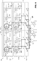
- FIG. 1 Illustrated schematically in Figure 1 and designated as a whole by the reference number 1 is a portion of a non-volatile memory device, in particular of a PCM type, limitedly to just the parts necessary for an understanding of the present disclosure.
- the non-volatile memory device 1 comprises a memory array 2, constituted by a plurality of first memory cells 3 (each including a phase-change region 3a and a local selection transistor 3b), and by a plurality of second memory cells 3' (each including a phase-change region 3a' and a local selection transistor 3b'), which can be selected by local wordlines WL and local bitlines BL.
- the second memory cells 3' correspond, as regards number and manufacturing characteristics, to the first memory cells 3 and, in use, store a logic datum complementary to that of the first memory cells 3.
- the second memory cells 3' are queried, during double-ended reading of the first memory cells 3, to read the logic datum stored in the first memory cells 3 by comparison with the logic datum stored in respective second memory cells 3'.
- Figure 1 illustrates first memory cells 3 (in the following also called “direct cells”) operatively coupled to respective local wordlines WL ⁇ > (WL ⁇ 0>, WL ⁇ 1>, ...) and to respective local bitlines BL L ⁇ > (BL L ⁇ 0>, BL L ⁇ 1>, ...), etc.
- second memory cells 3' in the following also called “complementary cells”, operatively coupled to the local wordlines WL ⁇ >, designated in Figure 1 as WL ⁇ 0>, WL ⁇ 1>, ..., and to respective local bitlines BL R ⁇ >, designated in Figure 1 as BL R ⁇ 0>, BL R ⁇ 1>, ..., etc.
- the local bitlines BL L ⁇ > and the first memory cells 3 form a first memory portion 2a.
- the local bitlines BL R ⁇ > and the second memory cells 3' form a second memory portion 2b.
- the phase-change element 3a, 3a' includes a phase-change material (for example, a chalcogenide), and is therefore able to store data in the form of levels of resistance associated to the different phases assumed by the phase-change material.
- the selector element 3b, 3b' is, for example, a PMOS transistor having its gate terminal connected to the respective wordline WL ⁇ >, a first conduction terminal connected to the phase-change element, and a second conduction terminal connected to a reference potential (for example, ground).
- the selector element is controlled so as to enable, when selected (i.e., switched on by the signal of the respective local wordline WL ⁇ > to which it is coupled), passage of a reading current through the phase-change element during an operation of reading of the logic datum stored therein.
- the non-volatile memory device 1 further comprises a row decoder (here not illustrated), adapted to select the local wordline WL ⁇ > corresponding to the memory cell 3, 3' each time to be addressed.
- a row decoder here not illustrated
- the memory array 2 is organized in a plurality of sectors (shown by way of example in the figure are only four sectors S1-S4).
- Each sector comprises respective local bitlines BL ⁇ > (direct bitlines BL L ⁇ > and complementary bitlines BL R ⁇ >), which can be addressed by a local column decoder 5 dedicated to each sector.
- the local bitlines BL ⁇ > of the sectors S1 and S2 can be addressed by an even number of addresses, and the respective sectors S1 and S2 may in what follows be referred to as "even sectors”.
- the local bitlines BL ⁇ > of the sectors S3 and S4 can be addressed by an odd number of addresses, and the respective sectors S3 and S4 may in what follows be referred to as "odd sectors”.
- activation of a local wordline WL ⁇ > and of a local bitline BL L,R ⁇ > enables unique selection of only one memory cell 3, 3'.
- a reading stage 7, of a type in itself known, is provided with a first sense amplifier 6a and a second sense amplifier 6b.
- the presence of two sense amplifiers 6a, 6b is dictated by the particular organization of the memory 1 where, to increase the reading speed, simultaneous reading of data different from one another is carried out (according to the even and odd division, mentioned previously and illustrated more fully hereinafter) by the two amplifiers 6a, 6b.
- the reading stage 7 is coupled to the local bitlines BL L,R ⁇ > by main bitlines MBL L ⁇ > (in the portion 2a) and main bitlines MBL R ⁇ > (in the portion 2b).
- a column decoder 4 (in the following also referred to as “global column decoder") is adapted to select the main bitline to which the memory cell 3, 3' to be addressed is coupled.
- the global column decoder 4 comprises, in an embodiment provided by way of example: a plurality of main selection switches 12a-12d coupled to main bitlines MBL L ⁇ > of the memory portion 2a; and a plurality of main selection switches 12e-12h coupled to main bitlines MBL R ⁇ > of the memory portion 2b.
- a first main bitline MBL L ⁇ 0> belonging to the memory portion 2a, connects the local bitlines BL L ⁇ > of the first sector S1 to the global column decoder 4 and, via the latter, to the reading stage 7.
- the first main bitline MBL L ⁇ 0> extends between a terminal of the main selection switch 12a and a node A common to all the local bitlines BL L ⁇ > belonging to the sector S1 in the first memory portion 2a (direct cells).
- the other terminal of the main selection switch 12a is coupled to a first input 6a' of the sense amplifier 6a.
- a second main bitline MBL L ⁇ 1> belonging to the memory portion 2a, connects the local bitlines BL L ⁇ > of the second sector S2 to the global column decoder 4 and, via the latter, to the reading stage 7.
- the second main bitline MBL L ⁇ 1> extends between a terminal of the main selection switch 12b and a node B common to all the local bitlines BL L ⁇ > belonging to the sector S2 in the first memory portion 2a (direct cells).
- the other terminal of the main selection switch 12b is coupled to the first input 6a' of the sense amplifier 6a.
- a third main bitline MBL L ⁇ 2> belonging to the memory portion 2a, connects the local bitlines BL L ⁇ > of the third sector S3 to the global column decoder 4 and, via the latter, to the reading stage 7.
- the third main bitline MBL L ⁇ 2> extends between a terminal of the main selection switch 12c and a node C common to all the local bitlines BL L ⁇ > belonging to the sector S3 in the first memory portion 2a (direct cells).
- the other terminal of the main selection switch 12c is coupled to a first input 6b' of the sense amplifier 6b.
- a fourth main bitline MBL L ⁇ 3> belonging to the memory portion 2a, connects the local bitlines BL L ⁇ > of the fourth sector S4 to the global column decoder 4 and, via the latter, to the reading stage 7.
- the fourth main bitline MBL L ⁇ 3> extends between a terminal of the main selection switch 12d and a node D common to all the local bitlines BL L ⁇ > belonging to the sector S4 in the first memory portion 2a (direct cells).
- the other terminal of the main selection switch 12d is coupled to the first input 6b' of the sense amplifier 6b.
- the memory portion 2b (complementary cells) is organized in a way similar to the memory portion 2a of the direct cells, as described hereinafter.
- the fifth main bitline MBL R ⁇ 0> extends between a terminal of the main selection switch 12e and a node E common to all the local bitlines BL R ⁇ > belonging to the sector S1 in the second memory portion 2b (complementary cells).
- the other terminal of the main selection switch 12e is coupled to a second input 6a" of the sense amplifier 6a.
- a sixth main bitline MBL R ⁇ 1> belonging to the memory portion 2b, connects the local bitlines BL R ⁇ > of the second sector S2 to the global column decoder 4 and, via the latter, to the reading stage 7.
- the sixth main bitline MBL R ⁇ 1> extends between a terminal of the main selection switch 12f and a node F common to all the local bitlines BL R ⁇ > belonging to the sector S2 in the second memory portion 2b (complementary cells).
- the other terminal of the main selection switch 12f is coupled to the second input 6a" of the sense amplifier 6a.
- a seventh main bitline MBL R ⁇ 2> belonging to the memory portion 2b, connects the local bitlines BL R ⁇ > of the third sector S3 to the global column decoder 4 and, via the latter, to the reading stage 7.
- the seventh main bitline MBL R ⁇ 2> extends between a terminal of the main selection switch 12g and a node G common to all the local bitlines BL R ⁇ > belonging to the sector S3 in the second memory portion 2b (complementary cells).
- the other terminal of the main selection switch 12g is coupled to a second input 6b" of the sense amplifier 6b.
- An eighth main bitline MBL R ⁇ 3> belonging to the memory portion 2b, connects the local bitlines BL R ⁇ > of the fourth sector S4 to the global column decoder 4 and, via the latter, to the reading stage 7.
- the fourth main bitline MBL L ⁇ 3> extends between a terminal of the main selection switch 12d and a node D common to all the local bitlines BL R ⁇ > belonging to the sector S4 in the first memory portion 2a (direct cells).
- the other terminal of the main selection switch 12d is coupled to the first input 6b' of the sense amplifier 6b.
- Each local bitline BL L ⁇ > of the sector S1 of the first memory portion 2a is electrically coupled to the node A by a respective local selection switch 13a (in the example of Figure 1 , local selection switches 13a are present in the form of PMOS transistors) .
- each local bitline BL R ⁇ > of the sector S1 of the second memory portion 2b is electrically coupled to the node E by a respective local selection switch 13b (in this example, PMOS transistors).
- each local bitline BL L ⁇ > of the sector S2 of the first memory portion 2a is electrically coupled to the node B by a respective local selection switch 13a (in the example of Figure 1 , local selection switches 13a are present in the form of PMOS transistors).
- each local bitline BL R ⁇ > of the sector S2 of the second memory portion 2b is electrically coupled to the node F by a respective local selection switch 13b (in this example, PMOS transistors).
- the local selection switches 13a, 13b form part of the respective local column decoders 5.
- the local column decoder 5 receives at input address-selection signals (also known as Decoded Address Signals, or DASs) S YO ⁇ > (in particular, S YO ⁇ 0>, ..., S YO ⁇ 1>, ...) for selecting a respective local bitline BL L ⁇ > (BL L ⁇ 0>, BL L ⁇ 1>, ...) and/or BL R ⁇ > (BL R ⁇ 0>, BL R ⁇ 1>, ...) in order to access the first memory cells 3 and/or the second memory cells 3'.
- DASs Decoded Address Signals
- the signals S YO ⁇ > are low-voltage signals, i.e., operating in the range of logic voltages [GND, VDD], where VDD is, for example, comprised between 1 V and 1.4 V and GND is a ground reference voltage, for example 0 V.
- the sense amplifier 6a is coupled to a subset of so-called even bitlines BL ⁇ > (i.e., indexed by an even index, such as BL ⁇ 0>, BL ⁇ 2>, BL ⁇ 4>, etc.) belonging to the sectors S1, S2, while the sense amplifier 6b is coupled to a subset of so-called odd bitlines BL ⁇ > (i.e., indexed by an odd index, such as BL ⁇ 1>, BL ⁇ 3>, BL ⁇ 5>, etc.) belonging to the sectors S3, S4.
- the reading operation is carried out at the same time by the sense amplifier 6a and 6b for the respective memory cells 3, 3' coupled, respectively, to the even and odd bitlines BL ⁇ >.
- the local column decoder 5 is configured so as to generate a current path between an even direct bitline selected from BL L ⁇ 0>, BL L ⁇ 2>, etc. (belonging to the portion 2a) and the first input 6a' of the sense amplifier 6a, and between an even complementary bitline selected from BL R ⁇ 0>, BL R ⁇ 2>, etc. (belonging to the portion 2b) and the second input 6a" of the sense amplifier 6a.
- the local column decoder 5 is configured so as to generate a current path between an odd direct bitline selected from BL L ⁇ 1>, BL L ⁇ 3>, etc. (belonging to the portion 2a) and the first input 6b' of the sense amplifier 6b, and between an odd complementary bitline selected from BL R ⁇ 1>, BL R ⁇ 3>, etc. (belonging to the portion 2b) and the second input 6b" of the sense amplifier 6b.
- sectors S1-S4 takes into account the reading division between even and odd.
- the sectors S1 and S2 group together bitlines that can be selected by even addresses
- the sectors S3 and S4 group together bitlines that can be selected by odd addresses.
- the main bitlines MBL L,R ⁇ 0,1> access even sectors S1 and S2; the main bitlines MBL L,R ⁇ 2,3> access odd sectors S3 and S4.
- the global column decoder 4 comprises two distinct read-decoding circuits, adapted to generate a respective current path between memory cells 3 of the portion 2a and the respective input 6a', 6b' of the sense amplifiers 6a, 6b, and between second memory cell 3' of the portion 2b and the respective input 6a", 6b" of the sense amplifiers 6a, 6b.
- the current paths thus generated are completely distinct and separate from one another.
- the two aforementioned read-decoding circuits of the global column decoder 4 present a specular circuit structure.
- the number of selection switches that form the global column decoder 4 depends upon the size of the memory array 2 and/or of the sectors of the memory array 2, as well as upon the hierarchical organization of the column selectors.
- the read-decoding circuits of the global column decoder 4 moreover comprise buffers (not illustrated) that drive the selection switches 12a-12h.
- Each buffer 9a receives a control signal S YN and supplies to the control terminals of the respective selection switches 12a-12h a column-decoding signal YN.
- Bitlines BL L ⁇ > belonging to the first portion 2a and corresponding to respective bitlines BL R ⁇ > of the second portion 2b of the memory array 2 can share a same local buffer.
- the local buffers are configured to receive a respective control signal S YO ⁇ > and supply to the control terminals of the respective local selection switches 13a, 13b column-decoding signals YO L ⁇ >, YO R ⁇ >.
- the selection switches of the circuit of Figure 1 are implemented by PMOS transistors, which have a control terminal (gate) that receives the respective column-decoding signals YN, YO L ⁇ >, YO R ⁇ >, which is a logic signal "0" that switches on the respective transistor, or else "1" that switches off the respective transistor.
- the signals S YO ⁇ > and S YN are low-voltage signals, and one of the operations carried out by the buffers is to raise said voltage by generating a voltage signal adequate for driving the respective PMOS transistor.
- the non-volatile memory device 1 further comprises a first reference branch 20 including a reference generator 21, configured to generate a reference current i REF , electrically coupled to the second input 6a" of the sense amplifier 6a by a selection switch 22.
- the selection switch 22 is driven by a signal Si', configured to switch on and switch off the selection switch 22 in respective operating modes of the non-volatile memory device 1 in order to set up or interrupt an electrical path for the reference current i REF towards the second input 6a" of the sense amplifier 6a.
- the non-volatile memory device 1 further comprises a second reference branch 23 including a reference generator 24, configured to generate a reference current i REF , electrically coupled to the second input 6b" of the sense amplifier 6b by a selection switch 25.
- the selection switch 25 is driven by a signal Si", configured to switch on and switch off the selection switch 25 in respective operating modes of the non-volatile memory device 1 in order to set up or interrupt an electrical path for the reference current i REF towards the second input 6b" of the sense amplifier 6b.
- each sense amplifier 6a, 6b by receiving at the respective inputs a datum (value of voltage/current) stored in a direct cell and a datum stored in a complementary cell.
- a datum value of voltage/current
- a datum value of voltage/current
- a complementary cell stored in a complementary cell.
- the respective (direct and complementary) cells that are being read belong to a same sector S1-S4, but to respective memory portions 2a, 2b.
- the connections between the memory cells and the sense amplifiers have been described previously.
- the reference generators 21, 24 are on, and reading is performed by comparing the current that flows in the memory cell selected with the reference current i REF .
- the global column decoder 4 is controlled so as to connect the inputs 6a", 6b" of the sense amplifiers 6a, 6b to a respective main bitline MBL R ⁇ > belonging to the memory portion 2b.
- the local column decoder 5 is controlled so as to connect said respective main bitlines MBL R ⁇ > to the local bitlines BL R ⁇ > of the respective memory sectors S1-S4.
- the wordlines WL ⁇ > are de-selected so that no specific memory cell 3' is in effect addressed.
- the only current that flows at the input 6a", 6b" of the sense amplifiers 6a, 6b is the respective reference current i REF .
- the capacitive load is, instead, given by the sum of the capacitances associated to the respective main and local bitlines that have been connected to the input 6a", 6b" of the sense amplifier 6a, 6b.
- Figure 2 corresponds, where not otherwise specified, to Figure 1 .
- the corresponding local selection switch 13a (delimited by a dashed circle in the sector S1, portion 2a) is switched on and the cell to be read is selected by activating the respective wordline WL (WL ⁇ 0> in Figure 2 ). Therefore, the main selector 12a is switched on, thus connecting the input 6a' of the amplifier 6a to the main bitline MBL L ⁇ 0>. In this way, an electrical connection is set up between the memory cell 3 to be read and the sense amplifier 6a. As has been said, supplied at the input 6a" is a reference current signal i REF .
- the local selection switch 13b delimited by a dashed circle in the sector S2, portion 2b is switched on, but no complementary memory cell is selected by the respective wordline WL ⁇ > (which remains de-selected).
- the main selector 12f is switched on to connect the main bitline MBL R ⁇ 1> to the local bitline BL R ⁇ > selected via the local selection switch that has been switched on.
- the other selectors 12b-12d, 12e, 12g, 12h remain off.
- the choice of switching on the selector 12f is dictated by the fact that this selector is coupled to the main bitline MBL R ⁇ 1>, which is in turn connected to the sector S2, i.e., to the sector physically "closest” to the sector S1 to which the direct memory cell to be read belongs.
- the two memory portions 2a, 2b are specular, we have the best guarantee of having a match that is as accurate as possible between the capacitive loads at the inputs 6a' and 6a".
- the capacitance associated to the main bitlines MBL L,R ⁇ > depends directly upon the length of said main bitlines MBL L,R ⁇ >.
- the present applicant has found that, to reduce the total area occupied by the memory array 2, it would be expedient to group memory sectors S1, S2, ..., etc. physically together. For instance, by grouping together the memory sector S2 and the memory sector S1, a new memory sector S1' would be obtained having a size equal to the sum of the sizes of the sectors S1 and S2 prior to grouping. In this way, there would be a saving of area given by the elimination of the local column decoders 5 associated to the sectors that have been eliminated (i.e., grouped together). In this example, the local column decoders 5 dedicated to the sector S2 would be eliminated. The entire new sector S1' would be handled by a local column decoder thereof.
- Patent document EP3509065 relates to a method for switching between different reading modes of a non-volatile memory, such a PCM.
- Patent document EP3544013 relates to a non-volatile memory device in which it is possible to switch between different reading modes.
- the aim of the present invention is consequently to provide a PCM device that will make it possible to solve, either totally or in part, the aforementioned problems, and that will be optimized as regards the characteristics of capacitive load seen by the sense amplifier in both the single-ended reading mode and the double-ended reading mode.
- the aim of the present invention is likewise to disclose a method for operating the PCM device.
- phase-change memory device a phase-change memory device, a system including the phase-change memory device, and a method for operating the phase-change memory device are consequently provided, as defined in the annexed claims.
- Illustrated schematically in Figure 3 and designated as a whole by the reference number 100 is a portion of a non-volatile memory device, in particular of a PCM type, limitedly to just the parts necessary for an understanding of the present disclosure.
- the non-volatile memory device 100 comprises a memory array 102, constituted by a plurality of first memory cells 3 and by a plurality of second memory cells 3', which can be selected by local wordlines WL and local bitlines BL.
- the second memory cells 3' correspond, in number and manufacturing characteristics, to the first memory cells 3 and, in use, store a logic datum complementary to that of the first memory cells 3.
- the second memory cells 3' are queried during double-ended reading of the first memory cells 3 to read the logic datum stored in the first memory cells 3 by comparison with the logic datum stored in respective second memory cells 3'.
- the local bitlines BL L ⁇ > and the first memory cells 3 form a first memory portion 102a.
- the local bitlines BL R ⁇ > and the second memory cells 3' form a second memory portion 102b.
- the memory array 102 is organized in at least a first sector S101 and a second sector S102.
- Each sector comprises respective local bitlines BL ⁇ > (direct bitlines BL L ⁇ >, and complementary bitlines BL R ⁇ >), which can be addressed by a local column decoder 5 for each sector.
- the local bitlines BL ⁇ > of the sector S101 can be addressed via an even address number (S101 is therefore also referred to as "even sector”), and the local bitlines BL ⁇ > of the sector S102 can be addressed via an odd address number (S102 is therefore also referred to as "odd sector").
- activation of a local wordline WL ⁇ > and of a local bitline BL L,R ⁇ > enables unique selection of only one memory cell 3, 3'.
- the reading stage 7 corresponds to what has already been described with reference to Figure 1 .
- the reading stage 7 is coupled to the local bitlines BL L,R ⁇ > by main bitlines MBL L ⁇ > (for the portion 2a) and main bitlines MBL R ⁇ > (for the portion 2b).
- the global column decoder 4 corresponds to what has already been described with reference to Figure 1 and is adapted to select the main bitline to which the memory cell 3, 3' to be addressed is coupled.
- a first main bitline MBL L ⁇ 0> belonging to the memory portion 2a, connects the local bitlines BL L ⁇ > of the sector S101 to the global column decoder 4 and, via the latter, to the reading stage 7.
- the first main bitline MBL L ⁇ 0> is connected to a node A common to all the local bitlines BL L ⁇ > belonging to the sector S101 in the first memory portion 2a (direct cells).
- both of the main selection switches 12a and 12d have a respective terminal connected to the first main bitline MBL L ⁇ 0>.
- the first main bitline MBL L ⁇ 0> extends between the node A and a node A', from which there branch off the connections towards the respective terminals of the main selection switches 12a and 12d.
- the other terminal of the main selection switch 12a is connected to the first input 6a' of the sense amplifier 6a.
- the other terminal of the main selection switch 12d is, instead, connected to the first input 6b' of the sense amplifier 6b.
- a second main bitline MBL L ⁇ 1> belonging to the memory portion 2a, connects the local bitlines BL L ⁇ > of the second sector S102 to the global column decoder 4 and, via the latter, to the reading stage 7.
- the second main bitline MBL L ⁇ 1> is connected to a node B common to all the local bitlines BL L ⁇ > belonging to the sector S102 in the first memory portion 2a (direct cells).
- both of the main selection switches 12b and 12c have a respective terminal connected to the second main bitline MBL L ⁇ 1>.
- the second main bitline MBL L ⁇ 1> extends between the node B and a node B', from which there branch off the connections towards the respective terminals of the main selection switches 12b and 12c.
- the other terminal of the main selection switch 12b is connected to the first input 6a' of the sense amplifier 6a.
- the other terminal of the main selection switch 12c is, instead, connected to the first input 6b' of the sense amplifier 6b.
- the memory portion 2b (complementary cells) is organized in a way similar to the memory portion 2a of the direct cells, as described hereinafter.
- a third main bitline MBL R ⁇ 0> belonging to the memory portion 2b, which connects the local bitlines BL R ⁇ > of the first sector S101 to the global column decoder 4 and, via the latter, to the reading stage 7.
- the third main bitline MBL R ⁇ 0> is connected to a node E common to all the local bitlines BL R ⁇ > belonging to the sector S101 in the second memory portion 2b (complementary cells).
- both of the main selection switches 12e and 12h have a respective terminal connected to the third main bitline MBL R ⁇ 0>.
- the third main bitline MBL R ⁇ 0> extends between the node E and a node E', from which there branch off the connections towards the respective terminals of the main selection switches 12e and 12h.
- the other terminal of the main selection switch 12e is connected to the second input 6a" of the sense amplifier 6a.
- the other terminal of the main selection switch 12h is, instead, connected to the second input 6b" of the sense amplifier 6b.
- a fourth main bitline MBL R ⁇ 1> belonging to the memory portion 2b, connects the local bitlines BL R ⁇ > of the second sector S102 to the global column decoder 4 and, via the latter, to the reading stage 7.
- the fourth main bitline MBL R ⁇ 1> is connected to a node G common to all the local bitlines BL R ⁇ > belonging to the sector S102 in the second memory portion 2b (complementary cells).
- both of the main selection switches 12g and 12f have a respective terminal connected to the fourth main bitline MBL R ⁇ 1>.
- the fourth main bitline MBL R ⁇ 1> extends between the node G and a node G', from which there branch off the connections towards the respective terminals of the main selection switches 12f and 12g.
- the other terminal of the main selection switch 12f is connected to the second input 6a" of the sense amplifier 6a.
- the other terminal of the main selection switch 12g is, instead, connected to the second input 6b" of the sense amplifier 6b.
- Each local bitline BL L ⁇ > of the sector S101 of the first memory portion 2a is electrically coupled to the node A by a respective local selection switch 13a (here, a respective PMOS transistor).
- each local bitline BL R ⁇ > of the sector S101 of the second memory portion 2b is electrically coupled to the node E by a respective local selection switch 13b (in this example, a respective PMOS transistor).
- each local bitline BL L ⁇ > of the sector S102 of the first memory portion 2a is electrically coupled to the node B by a respective local selection switch 13a (here, a respective PMOS transistor).
- each local bitline BL R ⁇ > of the sector S102 of the second memory portion 2b is electrically coupled to the node G by a respective local selection switch 13b (here, a respective PMOS transistor).
- the local selection switches 13a, 13b form part of the respective local column decoders 5.
- the local column decoder 5 receives at input address-selection signals (DAS) S YO ⁇ >, as already described with reference to Figure 1 and therefore not described any further here.
- DAS address-selection signals
- the sense amplifier 6a is coupled to a subset of bitlines BL ⁇ > referred to as even bitlines (i.e., indexed by an even index, such as BL ⁇ 0>, BL ⁇ 2>, BL ⁇ 4>, etc.) belonging to the sector 101, while the sense amplifier 6b is coupled to a subset of bitlines BL ⁇ > referred to as odd bitlines (i.e., indexed by an odd index, such as BL ⁇ 1>, BL ⁇ 3>, BL ⁇ 5>, etc.).
- the double-ended reading operation is carried out simultaneously by the sense amplifier 6a and 6b for the respective memory cells 3, 3' coupled, respectively, to the even and odd bitlines BL ⁇ >.
- the double-ended reading operation is carried out in accordance with the prior art, and is described by way of example hereinafter with reference to Figure 6 .
- the memory device 100 further comprises a first reference branch 20, which includes the reference generator 21, configured to generate the reference current i REF to be supplied to the second input 6a" of the sense amplifier 6a by the selection switch 22.
- the memory device 100 further comprises a second reference branch 23, which includes the reference generator 24, configured to generate a reference current i REF , and is electrically coupled to the second input 6b" of the sense amplifier 6b by the selection switch 25.
- the reference generators 21, 24 are on, and reading is performed by comparing the current that flows in the memory cell selected with the reference current i REF .
- the global column decoder 4 is controlled so as to connect the second inputs 6a", 6b" of the sense amplifiers 6a, 6b to a respective main bitline MBL R ⁇ > belonging to the memory portion 2b.
- the sector S102 is de-selected (i.e., no wordline of the sector S102 is selected), and the selection switches 12b-12d, 12e, 12g, 12h are switched off.
- the selection switches 12a, 12f are, instead, switched on. Reading is carried out by the sense amplifier 6a.
- reading of the logic datum stored in the memory cell 3 delimited by a dashed circle in the sector S101 is performed by connecting said memory cell 3 to the input 6a' of the sense amplifier 6a and enabling an electrical path between said memory cell 3 and the input 6a' (i.e., by selecting the corresponding wordline WL ⁇ 0> by switching on the switch 13a of the bitline BL ⁇ > coupled to the memory cell 3 to be read and switching on the selection switch 12a).
- the path of the reading current is indicated in Figure 4 with a thick solid line P1.
- the input 6a" receives the reference current i REF from the generator 21.
- the input 6a" is connected to the main bitline MBL R ⁇ 1> via the switch 12f, which is switched on.
- one of the switches 13b connected to the node G is also switched on, in particular the switch 13b for the bitline BL ⁇ > physically arranged so as to approximate as closely as possible the electrical path (and therefore the capacitive load) of the memory cell 3 to be read. Since all the wordlines WL ⁇ > of the sector S102 are de-selected, activation of the aforementioned electrical path does not generate a transfer of current towards the input 6a", but represents a capacitive load for the input 6a".
- Reading of a logic datum stored in a memory cell 3 of the sector S102 occurs in a way equivalent to what has been described with reference to Figure 4 . Also in this case, simultaneous reading of the even sector S101 and of the odd sector S102 is not possible in so far as there would cease to be a de-selected sector to be used for capacitive matching.
- the sector S101 is de-selected (i.e., no wordline of the sector S101 is selected), and the selection switches 12a, 12b, 12d, 12e-12g are switched off.
- the selection switches 12c, 12h are instead switched on. Reading is carried out by the sense amplifier 6b.
- reading of the logic datum stored in the memory cell 3 delimited by a dashed circle in the sector S102 occurs by connecting said memory cell 3 to the input 6b' of the sense amplifier 6b and enabling an electrical path between said memory cell 3 and the input 6b' (i.e., by selecting the corresponding wordline WL ⁇ > by switching on the switch 13a of the bitline BL ⁇ > coupled to the memory cell 3 to be read and switching on the selection switch 12c).
- the path of the reading current is indicated in Figure 5 with a thick solid line P3.
- the input 6b" receives the reference current i REF from the generator 24.
- the input 6b" is connected to the main bitline MBL R ⁇ 0> via the switch 12h, which is switched on.
- one of the switches 13b connected to the node E is switched on, in particular the switch 13b for the bitline BL ⁇ > physically arranged so as to approximate as closely as possible the electrical path (and therefore the capacitive load) of the memory cell 3 to be read. Since all the wordlines WL ⁇ > of the sector S101 are de-selected, activation of the aforementioned electrical path does not generate a transfer of current towards the input 6b", but represents a capacitive load for the input 6b". The path that forms said capacitive load is indicated in Figure 5 with a thick solid line P4. It may be noted that, in this reading condition, the sense amplifier 6a is off and does not receive any datum/current signal at its inputs 6a', 6a".
- the reference generators 21, 24 are off.
- the double-ended reading mode envisages ( Figure 6 ) simultaneously switching on the selection switches 12a, 12c, 12e, 12g, and keeping the remaining switches 12b, 12d, 12f, 12h off.
- the operations of activation or selection of the main and local bitlines, as likewise of the wordlines, to implement the single-ended and double-ended reading operations according to the present invention are carried out by a controller appropriately configured for this purpose, in a way in itself evident to the person skilled in the art.
- the controller governs the selectors (switches, which are constituted, in particular, by transistors) described previously, sending signals for switching them on and for switching them off so as to create the appropriate electrical connections with the inputs of the sense amplifiers 6a, 6b.
- Buffers (not illustrated in detail) are typically present to adapt the level of the (voltage/current) signal to the level accepted at input by the control terminal (gate) of the selectors.
- a controller 201 is illustrated by way of example in Figure 7 .
- FIG. 7 illustrates a portion of an electronic system 200, according to a further embodiment of the present invention.
- the electronic system 200 may be used in electronic devices, such as: a PDA (Personal Digital Assistant); a portable or fixed computer, possibly with the capacity of wireless data transfer; a mobile phone; a digital audio player; a photographic camera or video camera; or further devices capable of processing, storing, transmitting, and receiving information.
- PDA Personal Digital Assistant
- portable or fixed computer possibly with the capacity of wireless data transfer
- a mobile phone a digital audio player
- a photographic camera or video camera or further devices capable of processing, storing, transmitting, and receiving information.
- the electronic system 200 comprises a controller 201 (for example, provided with a microprocessor, a DSP, or a microcontroller), and the memory device 100, provided with the array of memory cells of the phase-change type, described previously.
- the electronic system 200 further comprises one or more from among an input/output device 202 (for example, provided with a keypad and a display) for entering and displaying data, a wireless interface 204, for example an antenna, for transmitting and receiving data through a wireless communication radiofrequency network, and a RAM 205, all of which are coupled through a bus 206.
- a battery 207 can be used as electrical supply source in the electronic system 200, which may moreover be provided with a photographic camera or video camera 208.
- the silicon area required for providing a non-volatile memory (in particular, a PCM) operating as described and having the circuit structure described is minimized.
- the architecture proposed moreover makes it possible to guarantee a good matching between the capacitive load and the inputs of the sense amplifier, both during single-ended reading and during double-ended reading.
- the selection switches 13b of the sector S102 could be off, whereas for reading of a memory cell of the sector S102 those of the sector S101 could be off.
- the most important capacitive component in PCMs is represented by the main bitline (which is typically obtained in the form of a conductive metal path with a length of 2 mm and a width of 1 ⁇ m). Consequently, also by turning off the switches 13b, there would in any case be guaranteed a comparable capacitive load on both of the inputs of the sense amplifier involved in the reading process.
- a PCM device typically comprises a plurality of sense amplifiers higher than two (e.g., 128, 256, etc.), each dedicated to reading in parallel of respective data coming from memory cells 3 and 3' (in the case of double-ended reading), or from a memory cell 3 and from a current reference (in the case of single-ended reading).
- one of the reference-current generators 21 and 24 may be omitted, and during single-ended reading the reference current i REF is supplied (alternatively) at the inputs 6a", 6b" by a single reference-current generator 21 or 24.
Landscapes
- Chemical & Material Sciences (AREA)
- Crystallography & Structural Chemistry (AREA)
- Semiconductor Memories (AREA)
- Dram (AREA)
- Static Random-Access Memory (AREA)
- Read Only Memory (AREA)
Abstract

Description
- The present invention relates to a phase-change memory device, to a system that includes the phase-change memory device, and to a method for operating the phase-change memory device.
- Non-volatile phase-change memories (PCMs) are known, in which for storing information the characteristics of materials that present the property of switching between phases that have different electrical characteristics are exploited. For instance, such materials are able to switch between a disorderly, amorphous, phase and an orderly, crystalline or polycrystalline, phase, and the two phases are associated to resistivities having considerably different values, and consequently to different values of a datum stored. For instance, the elements of Group VI of the Periodic Table, such as tellurium (Te), selenium (Se), or antimony (Sb), referred to as chalcogenides or chalcogenic materials, may advantageously be used for the production of phase-change memory cells. Phase-changes are obtained by locally increasing the temperature of the cells of chalcogenic material, through resistive electrodes (generally known as heaters) arranged in contact with respective regions of chalcogenic material. Selection devices (for example, MOSFETs) are connected to the heaters and enable passage of an electric programming current through a respective heater. Said electric current, by the Joule effect, generates the temperatures necessary for phase-change. During reading, the state of the chalcogenic material is detected by applying a voltage that is sufficiently low as not to cause a considerable heating, and then by reading the value of the current that flows in the cell. Given that the current is proportional to the conductivity of the chalcogenic material, it is possible to determine in which state the material is, and therefore to arrive at the datum stored in the memory cell.
- In a known way, non-volatile memories comprise an array of memory cells organised in rows (wordlines) and columns (bitlines). Each memory cell is constituted, in the case of PCMs, by a phase-change storage element and a selector transistor, connected in series. A column decoder and a row decoder enable selection, on the basis of address logic signals received at input and more or less complex decoding schemes, of the memory cells, and in particular of the corresponding wordline and bitline each time addressed.
- The column decoder comprises a plurality of analog selection switches (implemented by transistors), which receive at their respective control terminals the address signals. The selection switches are organized according to a tree structure in hierarchical levels, and their number in each hierarchical level is linked to the organization and size of the memory array. The selection switches, when enabled, make it possible to bring the bitline selected to a definite value of voltage and/or current, according to the operations that are to be implemented. In particular, a current path is created between a programming stage or a reading stage and the bitline selected. Said current path is defined by the series of a certain number of selection switches. In a known way, sense amplifiers carry out reading of the data stored in the memory cells, comparing the current that flows in the memory cell selected (or an electrical quantity correlated thereto) with a reference current that flows in a reference cell (so-called double-ended reading) or else with a reference current supplied by a reference-current generator (so-called single-ended reading). Single-ended reading is typically used during verification that programming of the cell has occurred or during testing, whereas double-ended reading is typically used during normal use of the memory to read the logic datum stored in the cell that is to be read.
- To carry out single-ended reading, an input of the sense amplifier receives the current of the memory cell that is to be read, while the other input of the sense amplifier receives the reference current supplied by the reference-current generator.
- In both of the modalities referred to it is expedient to guarantee, as far as possible, for the sense amplifier similar working conditions, with particular attention paid to the capacitive load at the two inputs thereof. This need, however, is unlikely to be met in single-ended reading systems in so far as, in a way in itself evident, the capacitance associated to a reference-current generator used in single-ended reading is different from the capacitance that derives from the bitline used for carrying the current signal of the cell that is to be read.
- In addition, it may be noted that the effective value of capacitance associated to the bitline is affected by a series of factors that are unforeseeable, such as the manufacturing process spread. Consequently, fluctuations may arise that do not render convenient the use of a pre-set capacitance associated to the reference-current generator.
- To overcome these drawbacks, it is known to connect the input of the sense amplifier that receives the reference current also to a de-selected memory cell (i.e., a cell that is turned off), through the respective bitlines. In this way, it is possible to guarantee a comparable capacitive load at the two inputs of the sense amplifier both in the operation of single-ended reading (reading of a logic datum stored in a memory cell by comparison with a current reference) and in the operation of double-ended reading (reading of a logic datum stored in a memory cell by comparison with a further memory cell).
- In particular, in the case of single-ended reading of a memory cell selected via the corresponding wordline and coupled to a local bitline of a memory sector, the sense amplifier will have, on a first input thereof, the capacitance associated to the local bitline plus the capacitance associated to a first main bitline to which the local bitline is connected. In addition, the sense amplifier will receive, on a second input thereof, the reference current used for the comparison but also a capacitance associated to a further main bitline, which, during this operation, is decoupled from local bitlines. In other words, the sense amplifier receives capacitive loads of a similar amount on both of the inputs.
- Illustrated schematically in
Figure 1 and designated as a whole by thereference number 1 is a portion of a non-volatile memory device, in particular of a PCM type, limitedly to just the parts necessary for an understanding of the present disclosure. - In particular, the
non-volatile memory device 1 comprises amemory array 2, constituted by a plurality of first memory cells 3 (each including a phase-change region 3a and alocal selection transistor 3b), and by a plurality ofsecond memory cells 3' (each including a phase-change region 3a' and alocal selection transistor 3b'), which can be selected by local wordlines WL and local bitlines BL. In a way in itself known, thesecond memory cells 3' correspond, as regards number and manufacturing characteristics, to thefirst memory cells 3 and, in use, store a logic datum complementary to that of thefirst memory cells 3. Thesecond memory cells 3' are queried, during double-ended reading of thefirst memory cells 3, to read the logic datum stored in thefirst memory cells 3 by comparison with the logic datum stored in respectivesecond memory cells 3'. -
Figure 1 illustrates first memory cells 3 (in the following also called "direct cells") operatively coupled to respective local wordlines WL<> (WL<0>, WL<1>, ...) and to respective local bitlines BLL<> (BLL<0>, BLL<1>, ...), etc. Likewise shown aresecond memory cells 3' (in the following also called "complementary cells"), operatively coupled to the local wordlines WL<>, designated inFigure 1 as WL<0>, WL<1>, ..., and to respective local bitlines BLR<>, designated inFigure 1 as BLR<0>, BLR<1>, ..., etc. - The local bitlines BLL<> and the
first memory cells 3 form afirst memory portion 2a. The local bitlines BLR<> and thesecond memory cells 3' form asecond memory portion 2b. - The phase-
change element selector element - The
non-volatile memory device 1 further comprises a row decoder (here not illustrated), adapted to select the local wordline WL<> corresponding to thememory cell - As represented schematically in
Figure 1 , thememory array 2 is organized in a plurality of sectors (shown by way of example in the figure are only four sectors S1-S4). Each sector comprises respective local bitlines BL<> (direct bitlines BLL<> and complementary bitlines BLR<>), which can be addressed by alocal column decoder 5 dedicated to each sector. The local bitlines BL<> of the sectors S1 and S2 can be addressed by an even number of addresses, and the respective sectors S1 and S2 may in what follows be referred to as "even sectors". The local bitlines BL<> of the sectors S3 and S4 can be addressed by an odd number of addresses, and the respective sectors S3 and S4 may in what follows be referred to as "odd sectors". - Given the matrix structure, activation of a local wordline WL<> and of a local bitline BLL,R<> enables unique selection of only one
memory cell - A
reading stage 7, of a type in itself known, is provided with afirst sense amplifier 6a and asecond sense amplifier 6b. The presence of twosense amplifiers memory 1 where, to increase the reading speed, simultaneous reading of data different from one another is carried out (according to the even and odd division, mentioned previously and illustrated more fully hereinafter) by the twoamplifiers - The
reading stage 7 is coupled to the local bitlines BLL,R<> by main bitlines MBLL<> (in theportion 2a) and main bitlines MBLR<> (in theportion 2b). - A column decoder 4 (in the following also referred to as "global column decoder") is adapted to select the main bitline to which the
memory cell global column decoder 4 comprises, in an embodiment provided by way of example: a plurality ofmain selection switches 12a-12d coupled to main bitlines MBLL<> of thememory portion 2a; and a plurality ofmain selection switches 12e-12h coupled to main bitlines MBLR<> of thememory portion 2b. - A first main bitline MBLL<0>, belonging to the
memory portion 2a, connects the local bitlines BLL<> of the first sector S1 to theglobal column decoder 4 and, via the latter, to thereading stage 7. In detail, the first main bitline MBLL<0> extends between a terminal of themain selection switch 12a and a node A common to all the local bitlines BLL<> belonging to the sector S1 in thefirst memory portion 2a (direct cells). The other terminal of themain selection switch 12a is coupled to afirst input 6a' of thesense amplifier 6a. - A second main bitline MBLL<1>, belonging to the
memory portion 2a, connects the local bitlines BLL<> of the second sector S2 to theglobal column decoder 4 and, via the latter, to thereading stage 7. In detail, the second main bitline MBLL<1> extends between a terminal of themain selection switch 12b and a node B common to all the local bitlines BLL<> belonging to the sector S2 in thefirst memory portion 2a (direct cells). The other terminal of themain selection switch 12b is coupled to thefirst input 6a' of thesense amplifier 6a. - A third main bitline MBLL<2>, belonging to the
memory portion 2a, connects the local bitlines BLL<> of the third sector S3 to theglobal column decoder 4 and, via the latter, to thereading stage 7. In detail, the third main bitline MBLL<2> extends between a terminal of themain selection switch 12c and a node C common to all the local bitlines BLL<> belonging to the sector S3 in thefirst memory portion 2a (direct cells). The other terminal of themain selection switch 12c is coupled to afirst input 6b' of thesense amplifier 6b. - A fourth main bitline MBLL<3>, belonging to the
memory portion 2a, connects the local bitlines BLL<> of the fourth sector S4 to theglobal column decoder 4 and, via the latter, to thereading stage 7. In detail, the fourth main bitline MBLL<3> extends between a terminal of themain selection switch 12d and a node D common to all the local bitlines BLL<> belonging to the sector S4 in thefirst memory portion 2a (direct cells). The other terminal of themain selection switch 12d is coupled to thefirst input 6b' of thesense amplifier 6b. - The
memory portion 2b (complementary cells) is organized in a way similar to thememory portion 2a of the direct cells, as described hereinafter. - There is thus present a fifth main bitline MBLR<0>, belonging to the
memory portion 2b, which connects the local bitlines BLR<> of the first sector S1 to theglobal column decoder 4 and, via the latter, to thereading stage 7. In detail, the fifth main bitline MBLR<0> extends between a terminal of themain selection switch 12e and a node E common to all the local bitlines BLR<> belonging to the sector S1 in thesecond memory portion 2b (complementary cells). The other terminal of themain selection switch 12e is coupled to asecond input 6a" of thesense amplifier 6a. - A sixth main bitline MBLR<1>, belonging to the
memory portion 2b, connects the local bitlines BLR<> of the second sector S2 to theglobal column decoder 4 and, via the latter, to thereading stage 7. In detail, the sixth main bitline MBLR<1> extends between a terminal of themain selection switch 12f and a node F common to all the local bitlines BLR<> belonging to the sector S2 in thesecond memory portion 2b (complementary cells). The other terminal of themain selection switch 12f is coupled to thesecond input 6a" of thesense amplifier 6a. - A seventh main bitline MBLR<2>, belonging to the
memory portion 2b, connects the local bitlines BLR<> of the third sector S3 to theglobal column decoder 4 and, via the latter, to thereading stage 7. In detail, the seventh main bitline MBLR<2> extends between a terminal of themain selection switch 12g and a node G common to all the local bitlines BLR<> belonging to the sector S3 in thesecond memory portion 2b (complementary cells). The other terminal of themain selection switch 12g is coupled to asecond input 6b" of thesense amplifier 6b. - An eighth main bitline MBLR<3>, belonging to the
memory portion 2b, connects the local bitlines BLR<> of the fourth sector S4 to theglobal column decoder 4 and, via the latter, to thereading stage 7. In detail, the fourth main bitline MBLL<3> extends between a terminal of themain selection switch 12d and a node D common to all the local bitlines BLR<> belonging to the sector S4 in thefirst memory portion 2a (direct cells). The other terminal of themain selection switch 12d is coupled to thefirst input 6b' of thesense amplifier 6b. - Each local bitline BLL<> of the sector S1 of the
first memory portion 2a is electrically coupled to the node A by a respectivelocal selection switch 13a (in the example ofFigure 1 ,local selection switches 13a are present in the form of PMOS transistors) . Likewise, each local bitline BLR<> of the sector S1 of thesecond memory portion 2b is electrically coupled to the node E by a respectivelocal selection switch 13b (in this example, PMOS transistors). - Likewise, each local bitline BLL<> of the sector S2 of the
first memory portion 2a is electrically coupled to the node B by a respectivelocal selection switch 13a (in the example ofFigure 1 ,local selection switches 13a are present in the form of PMOS transistors). Likewise, each local bitline BLR<> of the sector S2 of thesecond memory portion 2b is electrically coupled to the node F by a respectivelocal selection switch 13b (in this example, PMOS transistors). - The same structure is replicated in a similar way, and not described any further herein, for the remaining local bitlines BLL,R<> of the sectors S3 and S4.
- The
local selection switches local column decoders 5. - During use, the
local column decoder 5 receives at input address-selection signals (also known as Decoded Address Signals, or DASs) SYO<> (in particular, SYO<0>, ..., SYO<1>, ...) for selecting a respective local bitline BLL<> (BLL<0>, BLL<1>, ...) and/or BLR<> (BLR<0>, BLR<1>, ...) in order to access thefirst memory cells 3 and/or thesecond memory cells 3'. - The signals SYO<> are low-voltage signals, i.e., operating in the range of logic voltages [GND, VDD], where VDD is, for example, comprised between 1 V and 1.4 V and GND is a ground reference voltage, for example 0 V.
- As mentioned previously, to increase the reading parallelism, the
sense amplifier 6a is coupled to a subset of so-called even bitlines BL<> (i.e., indexed by an even index, such as BL<0>, BL<2>, BL<4>, etc.) belonging to the sectors S1, S2, while thesense amplifier 6b is coupled to a subset of so-called odd bitlines BL<> (i.e., indexed by an odd index, such as BL<1>, BL<3>, BL<5>, etc.) belonging to the sectors S3, S4. The reading operation is carried out at the same time by thesense amplifier respective memory cells - The
local column decoder 5 is configured so as to generate a current path between an even direct bitline selected from BLL<0>, BLL<2>, etc. (belonging to theportion 2a) and thefirst input 6a' of thesense amplifier 6a, and between an even complementary bitline selected from BLR<0>, BLR<2>, etc. (belonging to theportion 2b) and thesecond input 6a" of thesense amplifier 6a. - Furthermore, the
local column decoder 5 is configured so as to generate a current path between an odd direct bitline selected from BLL<1>, BLL<3>, etc. (belonging to theportion 2a) and thefirst input 6b' of thesense amplifier 6b, and between an odd complementary bitline selected from BLR<1>, BLR<3>, etc. (belonging to theportion 2b) and thesecond input 6b" of thesense amplifier 6b. - It may be noted that also the organization in sectors S1-S4 takes into account the reading division between even and odd. In fact, the sectors S1 and S2 group together bitlines that can be selected by even addresses, whereas the sectors S3 and S4 group together bitlines that can be selected by odd addresses. The main bitlines MBLL,R<0,1> access even sectors S1 and S2; the main bitlines MBLL,R<2,3> access odd sectors S3 and S4.
- In effect, the
global column decoder 4 comprises two distinct read-decoding circuits, adapted to generate a respective current path betweenmemory cells 3 of theportion 2a and therespective input 6a', 6b' of thesense amplifiers second memory cell 3' of theportion 2b and therespective input 6a", 6b" of thesense amplifiers - The two aforementioned read-decoding circuits of the
global column decoder 4 present a specular circuit structure. The number of selection switches that form theglobal column decoder 4 depends upon the size of thememory array 2 and/or of the sectors of thememory array 2, as well as upon the hierarchical organization of the column selectors. - The read-decoding circuits of the
global column decoder 4 moreover comprise buffers (not illustrated) that drive the selection switches 12a-12h. Each buffer 9a receives a control signal SYN and supplies to the control terminals of therespective selection switches 12a-12h a column-decoding signal YN. - Moreover a plurality of local buffers (not illustrated) is present. Bitlines BLL<> belonging to the
first portion 2a and corresponding to respective bitlines BLR<> of thesecond portion 2b of the memory array 2 (i.e., the bitlines selected by a same signal SYO<>) can share a same local buffer. The local buffers are configured to receive a respective control signal SYO<> and supply to the control terminals of the respectivelocal selection switches - The selection switches of the circuit of
Figure 1 are implemented by PMOS transistors, which have a control terminal (gate) that receives the respective column-decoding signals YN, YOL<>, YOR<>, which is a logic signal "0" that switches on the respective transistor, or else "1" that switches off the respective transistor. In use, the signals SYO<> and SYN are low-voltage signals, and one of the operations carried out by the buffers is to raise said voltage by generating a voltage signal adequate for driving the respective PMOS transistor. - The
non-volatile memory device 1 further comprises afirst reference branch 20 including areference generator 21, configured to generate a reference current iREF, electrically coupled to thesecond input 6a" of thesense amplifier 6a by aselection switch 22. Theselection switch 22 is driven by a signal Si', configured to switch on and switch off theselection switch 22 in respective operating modes of thenon-volatile memory device 1 in order to set up or interrupt an electrical path for the reference current iREF towards thesecond input 6a" of thesense amplifier 6a. - The
non-volatile memory device 1 further comprises asecond reference branch 23 including areference generator 24, configured to generate a reference current iREF, electrically coupled to thesecond input 6b" of thesense amplifier 6b by aselection switch 25. Theselection switch 25 is driven by a signal Si", configured to switch on and switch off theselection switch 25 in respective operating modes of thenon-volatile memory device 1 in order to set up or interrupt an electrical path for the reference current iREF towards thesecond input 6b" of thesense amplifier 6b. - During use of the
non-volatile memory device 1 in double-ended reading, thereference generators sense amplifier respective memory portions - Conversely, during use of the
non-volatile memory device 1 in single-ended reading, thereference generators sense amplifiers global column decoder 4 is controlled so as to connect theinputs 6a", 6b" of thesense amplifiers memory portion 2b. In addition, thelocal column decoder 5 is controlled so as to connect said respective main bitlines MBLR<> to the local bitlines BLR<> of the respective memory sectors S1-S4. However, the wordlines WL<> are de-selected so that nospecific memory cell 3' is in effect addressed. In this way, the only current that flows at theinput 6a", 6b" of thesense amplifiers input 6a", 6b" of thesense amplifier - To clarify the foregoing more fully, an example is proposed, with reference to
Figure 2 . -
Figure 2 corresponds, where not otherwise specified, toFigure 1 . - To read in single-ended mode a direct memory cell belonging to the sector S1, the corresponding
local selection switch 13a (delimited by a dashed circle in the sector S1,portion 2a) is switched on and the cell to be read is selected by activating the respective wordline WL (WL<0> inFigure 2 ). Therefore, themain selector 12a is switched on, thus connecting theinput 6a' of theamplifier 6a to the main bitline MBLL<0>. In this way, an electrical connection is set up between thememory cell 3 to be read and thesense amplifier 6a. As has been said, supplied at theinput 6a" is a reference current signal iREF. To provide at theinput 6a" a capacitive load comparable with the one present at theinput 6a', thelocal selection switch 13b delimited by a dashed circle in the sector S2,portion 2b, is switched on, but no complementary memory cell is selected by the respective wordline WL<> (which remains de-selected). Moreover, themain selector 12f is switched on to connect the main bitline MBLR<1> to the local bitline BLR<> selected via the local selection switch that has been switched on. Theother selectors 12b-12d, 12e, 12g, 12h remain off. It should be noted that the choice of switching on theselector 12f is dictated by the fact that this selector is coupled to the main bitline MBLR<1>, which is in turn connected to the sector S2, i.e., to the sector physically "closest" to the sector S1 to which the direct memory cell to be read belongs. In this way, since the twomemory portions inputs 6a' and 6a". In fact, the capacitance associated to the main bitlines MBLL,R<> depends directly upon the length of said main bitlines MBLL,R<>. It may be noted that it would not be possible to connect the main bitline MBLR<0> to theinput 6a" by switching on theselector 12e in so far as the wordline WL<> selected for accessing thememory cell 3 to be read is common to the entire sector S1, both in theportion 2a and in theportion 2b. Consequently, this condition is not practicable in single-ended reading. - A similar situation occurs for the reading performed by the
sense amplifier 6b. - The present applicant has found that, to reduce the total area occupied by the
memory array 2, it would be expedient to group memory sectors S1, S2, ..., etc. physically together. For instance, by grouping together the memory sector S2 and the memory sector S1, a new memory sector S1' would be obtained having a size equal to the sum of the sizes of the sectors S1 and S2 prior to grouping. In this way, there would be a saving of area given by the elimination of thelocal column decoders 5 associated to the sectors that have been eliminated (i.e., grouped together). In this example, thelocal column decoders 5 dedicated to the sector S2 would be eliminated. The entire new sector S1' would be handled by a local column decoder thereof. - However, grouping together of the sectors S2 and S1 would no longer make it possible, in the single-ended reading mode, to address properly the
memory cell 3 to be read and at the same time to guarantee the desired capacitive load at theinput 6a" of thesense amplifier 6a that receives the reference current iREF (as for theamplifier 6b). In fact, since it is not possible in this situation to connect theinput 6a" with the main bitline MBLR<1> of the second sector S2 (which has been eliminated), it would be necessary to use a further and different main bitline MBLR<>, losing at least in part the condition of matching of capacitances seen at the inputs of thesense amplifier 6a (likewise 6b). In fact, this grouping of sectors involves the use of a single column decoder for both of the sectors, which would therefore be addressed simultaneously. - Furthermore, by replicating the concept set forth above for all the even sectors and for all the odd sectors (i.e., by creating a single even sector accessible by just one local column decoder and a single odd sector accessible by just one, respective, local column decoder), it would not be possible to implement the strategy described above with reference to
Figure 2 , in so far as there would cease to be a de-selected sector to be used in single-ended reading to replicate the capacitive load at the terminal that receives the reference current iREF. - Patent document
EP3509065 relates to a method for switching between different reading modes of a non-volatile memory, such a PCM. - Patent document
EP3544013 relates to a non-volatile memory device in which it is possible to switch between different reading modes. - However, the above mentioned issues are not solved.
- The aim of the present invention is consequently to provide a PCM device that will make it possible to solve, either totally or in part, the aforementioned problems, and that will be optimized as regards the characteristics of capacitive load seen by the sense amplifier in both the single-ended reading mode and the double-ended reading mode. The aim of the present invention is likewise to disclose a method for operating the PCM device.
- According to the present invention, a phase-change memory device, a system including the phase-change memory device, and a method for operating the phase-change memory device are consequently provided, as defined in the annexed claims.
- For a better understanding of the present invention, preferred embodiments thereof are now described, purely by way of non-limiting example, with reference to the attached drawings, wherein:
-
Figure 1 is a schematic illustration of a portion of a non-volatile memory device, in particular of a PCM type, according to an embodiment that does not form part of the present invention; -
Figure 2 shows the memory device ofFigure 1 in an operating condition; -
Figure 3 is a schematic illustration of a portion of a non-volatile memory device, in particular of a PCM type, according to an embodiment of the present invention; -
Figures 4-6 represent the memory device ofFigure 3 in respective operating conditions of the present invention; and -
Figure 7 is a simplified block diagram of an electronic system incorporating the non-volatile memory device, in an embodiment of the present invention. - Illustrated schematically in
Figure 3 and designated as a whole by thereference number 100 is a portion of a non-volatile memory device, in particular of a PCM type, limitedly to just the parts necessary for an understanding of the present disclosure. - Elements of the
memory device 100 already described with reference toFigure 1 are not described any further here and are designated by the same reference numbers. - The
non-volatile memory device 100 comprises amemory array 102, constituted by a plurality offirst memory cells 3 and by a plurality ofsecond memory cells 3', which can be selected by local wordlines WL and local bitlines BL. In a way in itself known, thesecond memory cells 3' correspond, in number and manufacturing characteristics, to thefirst memory cells 3 and, in use, store a logic datum complementary to that of thefirst memory cells 3. Thesecond memory cells 3' are queried during double-ended reading of thefirst memory cells 3 to read the logic datum stored in thefirst memory cells 3 by comparison with the logic datum stored in respectivesecond memory cells 3'. - The local bitlines BLL<> and the
first memory cells 3 form afirst memory portion 102a. The local bitlines BLR<> and thesecond memory cells 3' form asecond memory portion 102b. - The
memory array 102 is organized in at least a first sector S101 and a second sector S102. Each sector comprises respective local bitlines BL<> (direct bitlines BLL<>, and complementary bitlines BLR<>), which can be addressed by alocal column decoder 5 for each sector. The local bitlines BL<> of the sector S101 can be addressed via an even address number (S101 is therefore also referred to as "even sector"), and the local bitlines BL<> of the sector S102 can be addressed via an odd address number (S102 is therefore also referred to as "odd sector"). - Given the matrix structure, activation of a local wordline WL<> and of a local bitline BLL,R<> enables unique selection of only one
memory cell - The
reading stage 7 corresponds to what has already been described with reference toFigure 1 . Thereading stage 7 is coupled to the local bitlines BLL,R<> by main bitlines MBLL<> (for theportion 2a) and main bitlines MBLR<> (for theportion 2b). - The
global column decoder 4 corresponds to what has already been described with reference toFigure 1 and is adapted to select the main bitline to which thememory cell - Here, a first main bitline MBLL<0>, belonging to the
memory portion 2a, connects the local bitlines BLL<> of the sector S101 to theglobal column decoder 4 and, via the latter, to thereading stage 7. The first main bitline MBLL<0> is connected to a node A common to all the local bitlines BLL<> belonging to the sector S101 in thefirst memory portion 2a (direct cells). As regards theglobal column decoder 4, both of the main selection switches 12a and 12d have a respective terminal connected to the first main bitline MBLL<0>. In other words, the first main bitline MBLL<0> extends between the node A and a node A', from which there branch off the connections towards the respective terminals of the main selection switches 12a and 12d. The other terminal of themain selection switch 12a is connected to thefirst input 6a' of thesense amplifier 6a. The other terminal of themain selection switch 12d is, instead, connected to thefirst input 6b' of thesense amplifier 6b. - A second main bitline MBLL<1>, belonging to the
memory portion 2a, connects the local bitlines BLL<> of the second sector S102 to theglobal column decoder 4 and, via the latter, to thereading stage 7. The second main bitline MBLL<1> is connected to a node B common to all the local bitlines BLL<> belonging to the sector S102 in thefirst memory portion 2a (direct cells). As regards theglobal column decoder 4, both of the main selection switches 12b and 12c have a respective terminal connected to the second main bitline MBLL<1>. In other words, the second main bitline MBLL<1> extends between the node B and a node B', from which there branch off the connections towards the respective terminals of the main selection switches 12b and 12c. The other terminal of themain selection switch 12b is connected to thefirst input 6a' of thesense amplifier 6a. The other terminal of themain selection switch 12c is, instead, connected to thefirst input 6b' of thesense amplifier 6b. - The
memory portion 2b (complementary cells) is organized in a way similar to thememory portion 2a of the direct cells, as described hereinafter. - There is thus present a third main bitline MBLR<0>, belonging to the
memory portion 2b, which connects the local bitlines BLR<> of the first sector S101 to theglobal column decoder 4 and, via the latter, to thereading stage 7. In detail, the third main bitline MBLR<0> is connected to a node E common to all the local bitlines BLR<> belonging to the sector S101 in thesecond memory portion 2b (complementary cells). As regards theglobal column decoder 4, both of the main selection switches 12e and 12h have a respective terminal connected to the third main bitline MBLR<0>. In other words, the third main bitline MBLR<0> extends between the node E and a node E', from which there branch off the connections towards the respective terminals of the main selection switches 12e and 12h. The other terminal of themain selection switch 12e is connected to thesecond input 6a" of thesense amplifier 6a. The other terminal of themain selection switch 12h is, instead, connected to thesecond input 6b" of thesense amplifier 6b. - A fourth main bitline MBLR<1>, belonging to the
memory portion 2b, connects the local bitlines BLR<> of the second sector S102 to theglobal column decoder 4 and, via the latter, to thereading stage 7. In detail, the fourth main bitline MBLR<1> is connected to a node G common to all the local bitlines BLR<> belonging to the sector S102 in thesecond memory portion 2b (complementary cells). As regards theglobal column decoder 4, both of the main selection switches 12g and 12f have a respective terminal connected to the fourth main bitline MBLR<1>. In other words, the fourth main bitline MBLR<1> extends between the node G and a node G', from which there branch off the connections towards the respective terminals of the main selection switches 12f and 12g. The other terminal of themain selection switch 12f is connected to thesecond input 6a" of thesense amplifier 6a. The other terminal of themain selection switch 12g is, instead, connected to thesecond input 6b" of thesense amplifier 6b. - Each local bitline BLL<> of the sector S101 of the
first memory portion 2a is electrically coupled to the node A by a respectivelocal selection switch 13a (here, a respective PMOS transistor). Likewise, each local bitline BLR<> of the sector S101 of thesecond memory portion 2b is electrically coupled to the node E by a respectivelocal selection switch 13b (in this example, a respective PMOS transistor). - Likewise, each local bitline BLL<> of the sector S102 of the
first memory portion 2a is electrically coupled to the node B by a respectivelocal selection switch 13a (here, a respective PMOS transistor). Likewise, each local bitline BLR<> of the sector S102 of thesecond memory portion 2b is electrically coupled to the node G by a respectivelocal selection switch 13b (here, a respective PMOS transistor). - The
local selection switches local column decoders 5. In use, thelocal column decoder 5 receives at input address-selection signals (DAS) SYO<>, as already described with reference toFigure 1 and therefore not described any further here. - As described with reference to
Figure 1 , also in this case thesense amplifier 6a is coupled to a subset of bitlines BL<> referred to as even bitlines (i.e., indexed by an even index, such as BL<0>, BL<2>, BL<4>, etc.) belonging to the sector 101, while thesense amplifier 6b is coupled to a subset of bitlines BL<> referred to as odd bitlines (i.e., indexed by an odd index, such as BL<1>, BL<3>, BL<5>, etc.). The double-ended reading operation is carried out simultaneously by thesense amplifier respective memory cells Figure 6 . - As regards reading in single-ended mode, the
memory device 100 further comprises afirst reference branch 20, which includes thereference generator 21, configured to generate the reference current iREF to be supplied to thesecond input 6a" of thesense amplifier 6a by theselection switch 22. Thememory device 100 further comprises asecond reference branch 23, which includes thereference generator 24, configured to generate a reference current iREF, and is electrically coupled to thesecond input 6b" of thesense amplifier 6b by theselection switch 25. - During use of the
memory device 100 in single-ended reading mode, thereference generators - In this reading mode, in order to maintain a same capacitive load on both of the inputs of the
sense amplifiers global column decoder 4 is controlled so as to connect thesecond inputs 6a", 6b" of thesense amplifiers memory portion 2b. - In this embodiment, however, simultaneous reading of the even sector S101 and of the odd sector S102 is not possible, in so far as there would cease to be a de-selected sector to be used for capacitive matching.
- Consequently, to read a datum from a
memory cell 3 of the sector S101, the sector S102 is de-selected (i.e., no wordline of the sector S102 is selected), and the selection switches 12b-12d, 12e, 12g, 12h are switched off. The selection switches 12a, 12f are, instead, switched on. Reading is carried out by thesense amplifier 6a. - As illustrated graphically in
Figure 4 , reading of the logic datum stored in thememory cell 3 delimited by a dashed circle in the sector S101 is performed by connecting saidmemory cell 3 to theinput 6a' of thesense amplifier 6a and enabling an electrical path between saidmemory cell 3 and theinput 6a' (i.e., by selecting the corresponding wordline WL<0> by switching on theswitch 13a of the bitline BL<> coupled to thememory cell 3 to be read and switching on theselection switch 12a). The path of the reading current is indicated inFigure 4 with a thick solid line P1. Theinput 6a" receives the reference current iREF from thegenerator 21. - In order to provide at the
input 6a" the required capacitive load, theinput 6a" is connected to the main bitline MBLR<1> via theswitch 12f, which is switched on. Moreover, one of theswitches 13b connected to the node G is also switched on, in particular theswitch 13b for the bitline BL<> physically arranged so as to approximate as closely as possible the electrical path (and therefore the capacitive load) of thememory cell 3 to be read. Since all the wordlines WL<> of the sector S102 are de-selected, activation of the aforementioned electrical path does not generate a transfer of current towards theinput 6a", but represents a capacitive load for theinput 6a". The path that constitutes said capacitive load is indicated inFigure 4 with a thick dashed line P2. It may be noted that, in this reading condition, thesense amplifier 6b is off and does not receive any datum/current signal at itsinputs 6b', 6b". - Reading of a logic datum stored in a
memory cell 3 of the sector S102 (odd sector) occurs in a way equivalent to what has been described with reference toFigure 4 . Also in this case, simultaneous reading of the even sector S101 and of the odd sector S102 is not possible in so far as there would cease to be a de-selected sector to be used for capacitive matching. - Consequently, to read a datum from a
memory cell 3 of the sector S102, the sector S101 is de-selected (i.e., no wordline of the sector S101 is selected), and theselection switches sense amplifier 6b. - As illustrated graphically in
Figure 5 , reading of the logic datum stored in thememory cell 3 delimited by a dashed circle in the sector S102 occurs by connecting saidmemory cell 3 to theinput 6b' of thesense amplifier 6b and enabling an electrical path between saidmemory cell 3 and theinput 6b' (i.e., by selecting the corresponding wordline WL<> by switching on theswitch 13a of the bitline BL<> coupled to thememory cell 3 to be read and switching on theselection switch 12c). The path of the reading current is indicated inFigure 5 with a thick solid line P3. Theinput 6b" receives the reference current iREF from thegenerator 24. - In order to provide at the
input 6b" the required capacitive load, theinput 6b" is connected to the main bitline MBLR<0> via theswitch 12h, which is switched on. In addition, also one of theswitches 13b connected to the node E is switched on, in particular theswitch 13b for the bitline BL<> physically arranged so as to approximate as closely as possible the electrical path (and therefore the capacitive load) of thememory cell 3 to be read. Since all the wordlines WL<> of the sector S101 are de-selected, activation of the aforementioned electrical path does not generate a transfer of current towards theinput 6b", but represents a capacitive load for theinput 6b". The path that forms said capacitive load is indicated inFigure 5 with a thick solid line P4. It may be noted that, in this reading condition, thesense amplifier 6a is off and does not receive any datum/current signal at itsinputs 6a', 6a". - During use of the
memory device 100 in double-ended reading mode, thereference generators Figure 6 ) simultaneously switching on theselection switches switches - In this way, by selecting (activating) the appropriate wordlines WL<> in both of the sectors S101, S102 (in order to select the direct memory cell to be read and, simultaneously, the respective complementary memory cell), it is possible to set up the desired current paths towards: the
input 6a' (path L1 inFigure 6 ); theinput 6a" (path L2 inFigure 6 ); theinput 6b' (path L3 inFigure 6 ); and theinput 6b" (path L4 inFigure 6 ). - The operations of activation or selection of the main and local bitlines, as likewise of the wordlines, to implement the single-ended and double-ended reading operations according to the present invention are carried out by a controller appropriately configured for this purpose, in a way in itself evident to the person skilled in the art. The controller governs the selectors (switches, which are constituted, in particular, by transistors) described previously, sending signals for switching them on and for switching them off so as to create the appropriate electrical connections with the inputs of the
sense amplifiers controller 201 is illustrated by way of example inFigure 7 . -
Figure 7 illustrates a portion of anelectronic system 200, according to a further embodiment of the present invention. Theelectronic system 200 may be used in electronic devices, such as: a PDA (Personal Digital Assistant); a portable or fixed computer, possibly with the capacity of wireless data transfer; a mobile phone; a digital audio player; a photographic camera or video camera; or further devices capable of processing, storing, transmitting, and receiving information. - In detail, the
electronic system 200 comprises a controller 201 (for example, provided with a microprocessor, a DSP, or a microcontroller), and thememory device 100, provided with the array of memory cells of the phase-change type, described previously. In addition and optionally, theelectronic system 200 further comprises one or more from among an input/output device 202 (for example, provided with a keypad and a display) for entering and displaying data, awireless interface 204, for example an antenna, for transmitting and receiving data through a wireless communication radiofrequency network, and aRAM 205, all of which are coupled through abus 206. Abattery 207 can be used as electrical supply source in theelectronic system 200, which may moreover be provided with a photographic camera orvideo camera 208. - From what has been described and illustrated previously, the advantages that the column decoder according to the invention affords are evident.
- In particular, the silicon area required for providing a non-volatile memory (in particular, a PCM) operating as described and having the circuit structure described is minimized.
- The architecture proposed moreover makes it possible to guarantee a good matching between the capacitive load and the inputs of the sense amplifier, both during single-ended reading and during double-ended reading.
- Finally, it is clear that modifications and variations may be made to what has been described and illustrated herein, without thereby departing from the scope of the present invention, as defined in the annexed claims.
- What has been described applies, in a similar way, to single-ended reading or double-ended reading of any
other memory cell 3. What has been described likewise applies, in a similar way, to verification in single-ended reading mode of thememory cells 3', using a current reference supplied to theinput 6a'/6b' of thesense amplifier 6a/6b. - It may be noted that, during single-ended reading of the sector S101 (
memory portion 102a), the selection switches 13b of the sector S102 could be off, whereas for reading of a memory cell of the sector S102 those of the sector S101 could be off. In fact, the most important capacitive component in PCMs is represented by the main bitline (which is typically obtained in the form of a conductive metal path with a length of 2 mm and a width of 1 µm). Consequently, also by turning off theswitches 13b, there would in any case be guaranteed a comparable capacitive load on both of the inputs of the sense amplifier involved in the reading process. - Moreover, the invention described and illustrated can be advantageously applied also to other types of memory devices, for example flash memory devices.
- It is evident that a different number of selection switches may be provided in the column decoder, and a different organization thereof in hierarchical levels.
- In addition, the present invention has been described with reference to just two
sense amplifiers memory cells memory cell 3 and from a current reference (in the case of single-ended reading). - Furthermore, one of the reference-
current generators inputs 6a", 6b" by a single reference-current generator
Claims (13)
- A phase-change memory device (100), comprising:- a memory array (102) including a first sector (S101) divided into a memory portion (102a) of first cells (3) and into a memory portion (102b) of second cells (3'), and a second sector (S102) divided into a respective memory portion (102a) of first cells (3) and into a respective memory portion (102b) of second cells (3');- a reading stage (6a, 6b) including a first sense amplifier (6a) configured to read a logic datum stored in a first cell (3) of the first sector (S101), and a second sense amplifier (6b) configured to read a logic datum stored in a first cell (3) of the second sector (S102);- a column decoder (4) functionally connected between the reading stage (6a, 6b) and the first and second sectors (S101, S102);- a first main bitline (MBLL<0>), having a first parasitic capacitance, which extends between the first cells (3) of the first sector (S101) and the column decoder (4);- a second main bitline (MBLR<0>), having a second parasitic capacitance, which extends between the second cells (3') of the first sector (S101) and the column decoder (4) ;- a third main bitline (MBLL<1>), having a third parasitic capacitance, which extends between the first cells (3) of the second sector (S102) and the column decoder (4);- a fourth main bitline (MBLR<1>), having a fourth parasitic capacitance, which extends between the second cells (3') of the second sector (S102) and the column decoder (4) ;- at least one reference-current generator (21; 24) coupled to the first and second sense amplifiers (6a, 6b) for supplying a reference reading current (iREF) during a first operating mode of single-ended reading; and- a controller (201) configured to execute, in order to read a logic datum stored in the first sector (S101) during the first operating mode, the operations of:- selecting a first cell (3) to be read belonging to the corresponding memory portion (102a) of the first sector (S101);- de-selecting all the second cells (3') belonging to the corresponding memory portion (102b) of the second sector (S102);- connecting, via the column decoder (4), the first main bitline (MBLL<0>) to a first input (6a') of the first sense amplifier (6a), thus coupling the first parasitic capacitance to the first input (6a') of the first sense amplifier (6a) and enabling a flow of current between the first cell (3) to be read in the first sector (S101) and the first input (6a') of the first sense amplifier (6a);- connecting the reference-current generator (21; 24) to a second input (6a") of the first sense amplifier (6a), thus enabling a flow of the reference reading current (iREF) towards the second input (6a") of the first sense amplifier (6a); and- connecting, via the column decoder (4), the fourth main bitline (MBLR<1>) to the second input (6a") of the first sense amplifier (6a), thus coupling the fourth parasitic capacitance to the second input (6a") of the first sense amplifier (6a),the controller (201) being moreover configured to execute, in order to read a logic datum stored in the second sector (S102) during the first operating mode, the operations of:- selecting a first cell (3) to be read belonging to the corresponding memory portion (102a) of the second sector (S102);- de-selecting all the second cells (3') belonging to the corresponding memory portion (102b) of the first sector (S101);- connecting, via the column decoder (4), the third main bitline (MBLL<1>) to a first input (6b') of the second sense amplifier (6b), thus coupling the third parasitic capacitance to the first input (6b') of the second sense amplifier (6b) and enabling a flow of current between the memory cell (3) to be read in the second sector (S102) and the first input (6b') of the second sense amplifier (6b);- connecting the reference-current generator (21; 24) to a second input (6b") of the second sense amplifier (6b), thus enabling a flow of the reference reading current (iREF) towards the second input (6b") of the second sense amplifier (6b); and- connecting, via the column decoder (4), the second main bitline (MBLR<0>) to the second input (6b") of the second sense amplifier (6b), thus coupling the second parasitic capacitance to the second input (6b") of the second sense amplifier (6b).
- The memory device according to claim 1, wherein each memory portion (102a) of first cells (3) of the first and second sectors (S101, S102) is provided with a plurality of first local bitlines (BLL<>) connected to the corresponding first cells (3), and wherein each memory portion (102b) of second cells (3') of the first and second sectors (S101, S102) is provided with a respective plurality of second local bitlines (BLR<>) connected to the corresponding second cells (3');
said first main bitline (MBLL<0>) extending at least in part between a first electrical node (A) common to all the first local bitlines (BLL<>) of the first sector (S101) and a second electrical node (A');
said second main bitline (MBLR<0>) extending at least in part between a third electrical node (E) common to all the second local bitlines (BLR<>) of the first sector (S101) and a fourth electrical node (E');
said third main bitline (MBLL<1>) extending at least in part between a fifth electrical node (B) common to all the first local bitlines (BLL<>) of the second sector (S102) and a sixth electrical node (B'); and
said fourth main bitline (MBLR<1>) extending at least in part between a seventh electrical node (G) common to all the second local bitlines (BLR<>) of the second sector (S102) and an eighth electrical node (G');
and wherein the column decoder (4) comprises a plurality of selection switches, amongst which:• a first selection switch (12a) connected between the second electrical node (A') and the first input (6a') of the first sense amplifier (6a);• a second selection switch (12d) connected between the second electrical node (A') and the first input (6b') of the second sense amplifier (6b);• a third selection switch (12c) connected between the sixth electrical node (B') and the first input (6b') of the second sense amplifier (6b);• a fourth selection switch (12b) connected between the sixth electrical node (B') and the first input (6a') of the first sense amplifier (6a);• a fifth selection switch (12e) connected between the fourth electrical node (E') and the second input (6a") of the first sense amplifier (6a);• a sixth selection switch (12h) connected between the fourth electrical node (E') and the second input (6b") of the second sense amplifier (6b);• a seventh selection switch (12g) connected between the eighth electrical node (G') and the second input (6b") of the second sense amplifier (6b); and• an eighth selection switch (12f) connected between the eighth electrical node (G') and the second input (6a") of the first sense amplifier (6a),wherein, to read a logic datum stored in the first sector (S101) during the first operating mode, the controller (201) is configured to:• switch on the first selection switch (12a) to connect the first main bitline (MBLL<0>) to the first input (6a') of the first sense amplifier (6a);• switch on the eighth selection switch (12f) to connect the fourth main bitline (MBLR<1>) to the second input (6a") of the first sense amplifier (6a); and• switch off the second, third, fourth, fifth, sixth, and seventh selection switches,and wherein, to read a logic datum stored in the second sector (S102) during the first operating mode, the controller (201) is configured to:• switch on the third selection switch (12c) to connect the third main bitline (MBLL<1>) to the first input (6b') of the second sense amplifier (6b);• switch on the sixth selection switch (12h) to connect the second main bitline (MBLR<0>) to the second input (6b") of the second sense amplifier (6b); and• switch off the first, second, fourth, fifth, seventh, and eighth selection switches. - The memory device according to claim 1 or claim 2, wherein each of said first and second cells (3, 3') comprises: a phase-change region (3a), which can be electrically connected to one of said first and second local bitlines (BLL<7:0>, BLR<7:0>), respectively; and a local selection transistor (3b), which is operatively coupled to said phase-change region (3a) and has a control terminal connected to a respective wordline (WL<>),
wherein the controller (201) is configured to:switch on the respective local selection transistor (3b) via the respective wordline (WL<>) in order to select a first cell (3) to be read; andswitch off the respective local selection transistor (3b) via the respective wordline (WL<>) in order to de-select the second cells (3'). - The memory device according to any one of the preceding claims, wherein the controller (201) is moreover configured to execute, during a second operating mode of double-ended reading of a logic datum stored in the first sector (S101), the operations of:- selecting a first cell (3) to be read belonging to the corresponding memory portion (102a) of the first sector (S101) and a respective second cell (3') belonging to the corresponding memory portion (102b) of the first sector (S101);- selecting a first cell (3) to be read belonging to the corresponding memory portion (102a) of the second sector (S102) and a respective second cell (3') belonging to the corresponding memory portion (102b) of the second sector (S102);- connecting, via the column decoder (4), the first main bitline (MBLL<0>) to the first input (6a') of the first sense amplifier (6a), thus coupling the first parasitic capacitance to the first input (6a') of the first sense amplifier (6a) and enabling a flow of current between the first cell (3) to be read in the first sector (S101) and the first input (6a') of the first sense amplifier (6a);- connecting, via the column decoder (4), the second main bitline (MBLR<0>) to the second input (6a") of the first sense amplifier (6a), thus coupling the second parasitic capacitance to the second input (6a") of the first sense amplifier (6a) and enabling a flow of current between the respective second cell (3') selected in the first sector (S101)and the second input (6a") of the first sense amplifier (6a);- connecting, via the column decoder (4), the third main bitline (MBLL<1>) to the first input (6b') of the second sense amplifier (6b), thus coupling the third parasitic capacitance to the first input (6b') of the second sense amplifier (6b) and enabling a flow of current between the first cell (3) to be read in the second sector (S102) and the first input (6b') of the second sense amplifier (6b);- connecting, via the column decoder (4), the fourth main bitline (MBLR<1>) to the second input (6b") of the second sense amplifier (6b), thus coupling the fourth parasitic capacitance to the second input (6b") of the second sense amplifier (6b) and enabling a flow of current between the respective second cell (3') selected in the second sector (S102) and the second input (6b") of the second sense amplifier (6b); and- electrically decoupling said reference-current generator (21; 24) from the first and second sense amplifiers (6a, 6b).
- The memory device according to claims 2 and 4, wherein the controller (201) is configured to:switch on the first selection switch (12a) and switch off the second selection switch (12d) in order to connect the first main bitline (MBLL<0>) to the first input (6a') of the first sense amplifier (6a);switch on the fifth selection switch (12e) and switch off the sixth selection switch (12h) in order to connect the second main bitline (MBLR<0>) to the second input (6a") of the first sense amplifier (6a);switch on the third selection switch (12c) and switch off the fourth selection switch (12b) in order to connect the third main bitline (MBLL<1>) to the first input (6b') of the second sense amplifier (6b);andswitch on the seventh selection switch (12g) and switch off the eighth selection switch (12f) in order to connect the fourth main bitline (MBLR<1>) to the second input (6b") of the second sense amplifier (6b).
- The memory device according to any one of the preceding claims, wherein the first operating mode is a mode of verification or testing of the logic datum stored in said memory cells of the first and second sectors (S101, S102).
- The memory device according to claim 4 or claim 5, or according to claim 6 when depending upon claim 4 or claim 5, wherein, in the second operating mode, the reading stage (7) is configured to read the logic datum stored in the selected first cell (3) via a comparison with a logic datum stored in the respective selected second cell (3') and belonging to the same first sector (S101) or second sector (S102) of the first cell (3).
- An electronic system (200), comprising a phase-change memory device (100) according to any one of claims 1-7.
- A method for read decoding of a phase-change memory device that comprises: a memory array (102) including a first sector (S101) divided into a memory portion (102a) of first cells (3) and a memory portion (102b) of second cells (3'), and a second sector (S102) divided into a respective memory portion (102a) of first cells (3) and a respective memory portion (102b) of second cells (3'); a reading stage (6a, 6b) including a first sense amplifier (6a) configured to read a logic datum stored in a first cell of the first sector (S101), and a second sense amplifier (6b) configured to read a logic datum stored in a first cell of the second sector (S102); a column decoder (4) functionally connected between the reading stage (6a, 6b) and the first and second sectors (S101, S102); a first main bitline (MBLL<0>), having a first parasitic capacitance, which extends between the first cells (3) of the first sector (S101) and the column decoder (4); a second main bitline (MBLR<0>) having a second parasitic capacitance, which extends between the second cells (3') of the first sector (S101) and the column decoder (4); a third main bitline (MBLL<1>), having a third parasitic capacitance, which extends between the first cells (3) of the second sector (S102) and the column decoder (4); a fourth main bitline (MBLR<1>) having a fourth parasitic capacitance, which extends between the second cells (3') of the second sector (S102) and the column decoder (4); and at least one reference-current generator (21; 24) coupled to the first and second sense amplifiers (6a, 6b) for supplying a reference reading current (iREF) during a first operating mode,
the method comprising, during the first operating mode and for reading a logic datum stored in the first sector (S101), the steps of:- selecting a first cell (3) to be read belonging to the corresponding memory portion (102a) of the first sector (S101);- de-selecting all the second cells (3') belonging to the respective memory portion (102b) of the second sector (S102);- connecting, via the column decoder (4), the first main bitline (MBLL<0>) to a first input (6a') of the first sense amplifier (6a);- connecting the reference-current generator (21; 24) to a second input (6a") of the first sense amplifier (6a); and- connecting, via the column decoder (4), the fourth main bitline (MBLR<1>) to the second input (6a") of the first sense amplifier (6a),the method further comprising, during the first operating mode and for reading a logic datum stored in the second sector (S102), the steps of:- selecting a first cell (3) to be read belonging to the respective memory portion (102a) of the second sector (S102);- de-selecting all the second cells (3') belonging to the respective memory portion (102b) of the first sector (S101) ;- connecting, via the column decoder (4), the third main bitline (MBLL<1>) to a first input (6b') of the second sense amplifier (6b);- connecting the reference-current generator (21; 24) to a second input (6b") of the second sense amplifier (6b); and- connecting, via the column decoder (4), the second main bitline (MBLR<0>) to the second input (6b") of the second sense amplifier (6b). - The method according to claim 9, wherein each of said first and second cells (3, 3') comprises: a phase-change region (3a), which can be electrically connected to one of said first and second local bitlines (BLL<7:0>, BLR<7:0>), respectively; and a local selection transistor (3b), operatively coupled to said phase-change region (3a) and having a control terminal connected to a respective wordline (WL<>),
wherein the steps of selecting a first cell (3) to be read include switching on the respective local selection transistor (3b) via the respective wordline (WL<>), and said steps of de-selecting the second cells (3') include switching off the respective local selection transistor (3b) via the respective wordline (WL<>). - The method according to any one of the preceding claims, further comprising the step of operating in a second operating mode of double-ended reading of a logic datum stored in the first sector (S101), which includes the substeps of:- selecting a first cell (3) to be read belonging to the corresponding memory portion (102a) of the first sector (S101) and a respective second cell (3') belonging to the corresponding memory portion (102b) of the first sector (S101);- selecting a first cell (3) to be read belonging to the corresponding memory portion (102a) of the second sector (S102) and a respective second cell (3') belonging to the corresponding memory portion (102b) of the second sector (S102);- connecting, via the column decoder (4), the first main bitline (MBLL<0>) to the first input (6a') of the first sense amplifier (6a), thus coupling the first parasitic capacitance to the first input (6a') of the first sense amplifier (6a) and enabling a flow of current between the first cell (3) to be read in the first sector (S101) and the first input (6a') of the first sense amplifier (6a);- connecting, via the column decoder (4), the second main bitline (MBLR<0>) to the second input (6a") of the first sense amplifier (6a), thus coupling the second parasitic capacitance to the second input (6a") of the first sense amplifier (6a) and enabling a flow of current between the respective second cell (3') selected in the first sector (S101), and the second input (6a") of the first sense amplifier (6a);- connecting, via the column decoder (4), the third main bitline (MBLL<1>) to the first input (6b') of the second sense amplifier (6b), thus coupling the third parasitic capacitance to the first input (6b') of the second sense amplifier (6b) and enabling a flow of current between the first cell (3) to be read in the second sector (S102) and the first input (6b') of the second sense amplifier (6b);- connecting, via the column decoder (4), the fourth main bitline (MBLR<1>) to the second input (6b") of the second sense amplifier (6b), thus coupling the fourth parasitic capacitance to the second input (6b") of the second sense amplifier (6b) and enabling a flow of current between the respective second cell (3') selected in the second sector (S102) and the second input (6b") of the second sense amplifier (6b); and- electrically decoupling said reference-current generator (21; 24) from the first and second sense amplifiers (6a, 6b).
- The method according to any one of claims 9-11, wherein the first operating mode is a mode of verification or testing of the logic datum stored in said memory cells of the first and second sectors (S101, S102).
- The method according to claim 11, or according to claim 12 when depending upon claim 11, wherein, in the second operating mode, the logic datum stored in the first cell (3) selected is read by the reading stage (7) via comparison with a logic datum stored in the respective second cell (3') selected belonging to the same first sector (S101) or second sector (S102) of the first cell (3).
Applications Claiming Priority (1)
| Application Number | Priority Date | Filing Date | Title |
|---|---|---|---|
| IT102019000024253A IT201900024253A1 (en) | 2019-12-17 | 2019-12-17 | PHASE CHANGE MEMORY DEVICE WITH REDUCED AREA CONSUMPTION, SYSTEM INCLUDING THE MEMORY DEVICE AND OPERATING METHOD OF THE PHASE CHANGE MEMORY DEVICE |
Publications (2)
| Publication Number | Publication Date |
|---|---|
| EP3839957A1 true EP3839957A1 (en) | 2021-06-23 |
| EP3839957B1 EP3839957B1 (en) | 2025-06-04 |
Family
ID=69904117
Family Applications (1)
| Application Number | Title | Priority Date | Filing Date |
|---|---|---|---|
| EP20215193.2A Active EP3839957B1 (en) | 2019-12-17 | 2020-12-17 | Phase-change memory device with reduced area consumption, system including the memory device and method for operating the phase-change memory device |
Country Status (4)
| Country | Link |
|---|---|
| US (2) | US11328768B2 (en) |
| EP (1) | EP3839957B1 (en) |
| CN (1) | CN112992228B (en) |
| IT (1) | IT201900024253A1 (en) |
Families Citing this family (1)
| Publication number | Priority date | Publication date | Assignee | Title |
|---|---|---|---|---|
| IT201900024253A1 (en) * | 2019-12-17 | 2021-06-17 | St Microelectronics Srl | PHASE CHANGE MEMORY DEVICE WITH REDUCED AREA CONSUMPTION, SYSTEM INCLUDING THE MEMORY DEVICE AND OPERATING METHOD OF THE PHASE CHANGE MEMORY DEVICE |
Citations (2)
| Publication number | Priority date | Publication date | Assignee | Title |
|---|---|---|---|---|
| EP3509065A1 (en) | 2018-01-09 | 2019-07-10 | STMicroelectronics S.r.l. | A device for switching between different reading modes of a non-volatile memory and method for reading a non-volatile memory |
| EP3544013A1 (en) | 2018-03-20 | 2019-09-25 | STMicroelectronics S.r.l. | A non-volatile memory device with switchable reading mode and related reading method |
Family Cites Families (9)
| Publication number | Priority date | Publication date | Assignee | Title |
|---|---|---|---|---|
| JP4381278B2 (en) * | 2004-10-14 | 2009-12-09 | 株式会社東芝 | Control method of nonvolatile semiconductor memory device |
| US20110058135A1 (en) * | 2008-05-26 | 2011-03-10 | Sharp Kabushiki Kaisha | Display device |
| ITTO20080645A1 (en) * | 2008-08-29 | 2010-02-28 | St Microelectronics Srl | ROW DECODER FOR NON-VOLATILE MEMORY DEVICES, IN PARTICULAR OF THE PHASE CHANGE TYPE |
| JP2010182353A (en) * | 2009-02-04 | 2010-08-19 | Elpida Memory Inc | Semiconductor memory device and reading method therefor |
| US8867260B2 (en) * | 2012-04-24 | 2014-10-21 | Agency For Science, Technology And Research | Reading circuit for a resistive memory cell |
| US9281061B2 (en) * | 2012-09-19 | 2016-03-08 | Micron Technology, Inc. | Methods and apparatuses having a voltage generator with an adjustable voltage drop for representing a voltage drop of a memory cell and/or a current mirror circuit and replica circuit |
| US9613692B1 (en) * | 2015-12-16 | 2017-04-04 | Stmicroelectronics International N.V. | Sense amplifier for non-volatile memory devices and related methods |
| IT201700114539A1 (en) * | 2017-10-11 | 2019-04-11 | St Microelectronics Srl | CIRCUIT AND READING METHOD WITH IMPROVED ELECTRICAL FEATURES FOR A NON-VOLATILE MEMORY DEVICE |
| IT201900024253A1 (en) * | 2019-12-17 | 2021-06-17 | St Microelectronics Srl | PHASE CHANGE MEMORY DEVICE WITH REDUCED AREA CONSUMPTION, SYSTEM INCLUDING THE MEMORY DEVICE AND OPERATING METHOD OF THE PHASE CHANGE MEMORY DEVICE |
-
2019
- 2019-12-17 IT IT102019000024253A patent/IT201900024253A1/en unknown
-
2020
- 2020-12-11 US US17/119,979 patent/US11328768B2/en active Active
- 2020-12-17 EP EP20215193.2A patent/EP3839957B1/en active Active
- 2020-12-17 CN CN202011500455.1A patent/CN112992228B/en active Active
-
2022
- 2022-04-04 US US17/657,861 patent/US11756614B2/en active Active
Patent Citations (2)
| Publication number | Priority date | Publication date | Assignee | Title |
|---|---|---|---|---|
| EP3509065A1 (en) | 2018-01-09 | 2019-07-10 | STMicroelectronics S.r.l. | A device for switching between different reading modes of a non-volatile memory and method for reading a non-volatile memory |
| EP3544013A1 (en) | 2018-03-20 | 2019-09-25 | STMicroelectronics S.r.l. | A non-volatile memory device with switchable reading mode and related reading method |
Also Published As
| Publication number | Publication date |
|---|---|
| CN112992228A (en) | 2021-06-18 |
| US20210193220A1 (en) | 2021-06-24 |
| IT201900024253A1 (en) | 2021-06-17 |
| US11756614B2 (en) | 2023-09-12 |
| EP3839957B1 (en) | 2025-06-04 |
| CN112992228B (en) | 2025-02-28 |
| US11328768B2 (en) | 2022-05-10 |
| US20220230682A1 (en) | 2022-07-21 |
Similar Documents
| Publication | Publication Date | Title |
|---|---|---|
| EP2159800B1 (en) | Row decoder for non-volatile memory devices, in particular of the phase-change type | |
| EP3509065B1 (en) | A device for switching between different reading modes of a non-volatile memory and method for reading a non-volatile memory | |
| US10593400B2 (en) | Row decoding architecture for a phase-change non-volatile memory device and corresponding row decoding method | |
| US8264872B2 (en) | Column decoder for non-volatile memory devices, in particular of the phase-change type | |
| US11289158B2 (en) | Non-volatile memory device including a row decoder with a pull-up stage controlled by a current mirror | |
| US11049561B2 (en) | Method for programming a phase-change memory device of differential type, memory device, and electronic system | |
| JP5518441B2 (en) | Low power access method for phase change memory device | |
| US10186317B2 (en) | Phase change memory device and method of operation | |
| US11756614B2 (en) | Phase change memory device, system including the memory device, and method for operating the memory device | |
| US11380380B2 (en) | Non volatile memory device with an asymmetric row decoder and method for selecting word lines | |
| US12482521B2 (en) | Non-volatile phase-change memory device including a distributed row decoder with n-channel MOSFET transistors and related row decoding method | |
| US11908514B2 (en) | Non-volatile phase-change memory device including a distributed row decoder with n-channel MOSFET transistors and related row decoding method | |
| EP3817001B1 (en) | Method for programming a phase-change memory device of differential type, phase-change memory device, and electronic system | |
| US10522220B2 (en) | Phase change memory device with selector MOS transistors and source line clustering | |
| US20180122470A1 (en) | Non-volatile memory, system including the memory and method for controlling the memory |
Legal Events
| Date | Code | Title | Description |
|---|---|---|---|
| PUAI | Public reference made under article 153(3) epc to a published international application that has entered the european phase |
Free format text: ORIGINAL CODE: 0009012 |
|
| STAA | Information on the status of an ep patent application or granted ep patent |
Free format text: STATUS: THE APPLICATION HAS BEEN PUBLISHED |
|
| AK | Designated contracting states |
Kind code of ref document: A1 Designated state(s): AL AT BE BG CH CY CZ DE DK EE ES FI FR GB GR HR HU IE IS IT LI LT LU LV MC MK MT NL NO PL PT RO RS SE SI SK SM TR |
|
| STAA | Information on the status of an ep patent application or granted ep patent |
Free format text: STATUS: REQUEST FOR EXAMINATION WAS MADE |
|
| 17P | Request for examination filed |
Effective date: 20211027 |
|
| RBV | Designated contracting states (corrected) |
Designated state(s): AL AT BE BG CH CY CZ DE DK EE ES FI FR GB GR HR HU IE IS IT LI LT LU LV MC MK MT NL NO PL PT RO RS SE SI SK SM TR |
|
| STAA | Information on the status of an ep patent application or granted ep patent |
Free format text: STATUS: EXAMINATION IS IN PROGRESS |
|
| 17Q | First examination report despatched |
Effective date: 20221205 |
|
| GRAP | Despatch of communication of intention to grant a patent |
Free format text: ORIGINAL CODE: EPIDOSNIGR1 |
|
| STAA | Information on the status of an ep patent application or granted ep patent |
Free format text: STATUS: GRANT OF PATENT IS INTENDED |
|
| INTG | Intention to grant announced |
Effective date: 20241015 |
|
| GRAJ | Information related to disapproval of communication of intention to grant by the applicant or resumption of examination proceedings by the epo deleted |
Free format text: ORIGINAL CODE: EPIDOSDIGR1 |
|
| STAA | Information on the status of an ep patent application or granted ep patent |
Free format text: STATUS: EXAMINATION IS IN PROGRESS |
|
| GRAP | Despatch of communication of intention to grant a patent |
Free format text: ORIGINAL CODE: EPIDOSNIGR1 |
|
| STAA | Information on the status of an ep patent application or granted ep patent |
Free format text: STATUS: GRANT OF PATENT IS INTENDED |
|
| GRAJ | Information related to disapproval of communication of intention to grant by the applicant or resumption of examination proceedings by the epo deleted |
Free format text: ORIGINAL CODE: EPIDOSDIGR1 |
|
| STAA | Information on the status of an ep patent application or granted ep patent |
Free format text: STATUS: EXAMINATION IS IN PROGRESS |
|
| GRAP | Despatch of communication of intention to grant a patent |
Free format text: ORIGINAL CODE: EPIDOSNIGR1 |
|
| STAA | Information on the status of an ep patent application or granted ep patent |
Free format text: STATUS: GRANT OF PATENT IS INTENDED |
|
| INTC | Intention to grant announced (deleted) | ||
| INTG | Intention to grant announced |
Effective date: 20250103 |
|
| GRAS | Grant fee paid |
Free format text: ORIGINAL CODE: EPIDOSNIGR3 |
|
| GRAA | (expected) grant |
Free format text: ORIGINAL CODE: 0009210 |
|
| STAA | Information on the status of an ep patent application or granted ep patent |
Free format text: STATUS: THE PATENT HAS BEEN GRANTED |
|
| AK | Designated contracting states |
Kind code of ref document: B1 Designated state(s): AL AT BE BG CH CY CZ DE DK EE ES FI FR GB GR HR HU IE IS IT LI LT LU LV MC MK MT NL NO PL PT RO RS SE SI SK SM TR |
|
| REG | Reference to a national code |
Ref country code: GB Ref legal event code: FG4D |
|
| REG | Reference to a national code |
Ref country code: CH Ref legal event code: EP |
|
| REG | Reference to a national code |
Ref country code: DE Ref legal event code: R096 Ref document number: 602020052234 Country of ref document: DE |
|
| REG | Reference to a national code |
Ref country code: IE Ref legal event code: FG4D |
|
| REG | Reference to a national code |
Ref country code: NL Ref legal event code: MP Effective date: 20250604 |
|
| PG25 | Lapsed in a contracting state [announced via postgrant information from national office to epo] |
Ref country code: FI Free format text: LAPSE BECAUSE OF FAILURE TO SUBMIT A TRANSLATION OF THE DESCRIPTION OR TO PAY THE FEE WITHIN THE PRESCRIBED TIME-LIMIT Effective date: 20250604 Ref country code: ES Free format text: LAPSE BECAUSE OF FAILURE TO SUBMIT A TRANSLATION OF THE DESCRIPTION OR TO PAY THE FEE WITHIN THE PRESCRIBED TIME-LIMIT Effective date: 20250604 |
|
| REG | Reference to a national code |
Ref country code: LT Ref legal event code: MG9D |
|
| PG25 | Lapsed in a contracting state [announced via postgrant information from national office to epo] |
Ref country code: NO Free format text: LAPSE BECAUSE OF FAILURE TO SUBMIT A TRANSLATION OF THE DESCRIPTION OR TO PAY THE FEE WITHIN THE PRESCRIBED TIME-LIMIT Effective date: 20250904 Ref country code: GR Free format text: LAPSE BECAUSE OF FAILURE TO SUBMIT A TRANSLATION OF THE DESCRIPTION OR TO PAY THE FEE WITHIN THE PRESCRIBED TIME-LIMIT Effective date: 20250905 |
|
| PG25 | Lapsed in a contracting state [announced via postgrant information from national office to epo] |
Ref country code: PL Free format text: LAPSE BECAUSE OF FAILURE TO SUBMIT A TRANSLATION OF THE DESCRIPTION OR TO PAY THE FEE WITHIN THE PRESCRIBED TIME-LIMIT Effective date: 20250604 |
|
| PG25 | Lapsed in a contracting state [announced via postgrant information from national office to epo] |
Ref country code: BG Free format text: LAPSE BECAUSE OF FAILURE TO SUBMIT A TRANSLATION OF THE DESCRIPTION OR TO PAY THE FEE WITHIN THE PRESCRIBED TIME-LIMIT Effective date: 20250604 |
|
| PG25 | Lapsed in a contracting state [announced via postgrant information from national office to epo] |
Ref country code: HR Free format text: LAPSE BECAUSE OF FAILURE TO SUBMIT A TRANSLATION OF THE DESCRIPTION OR TO PAY THE FEE WITHIN THE PRESCRIBED TIME-LIMIT Effective date: 20250604 |
|
| PG25 | Lapsed in a contracting state [announced via postgrant information from national office to epo] |
Ref country code: RS Free format text: LAPSE BECAUSE OF FAILURE TO SUBMIT A TRANSLATION OF THE DESCRIPTION OR TO PAY THE FEE WITHIN THE PRESCRIBED TIME-LIMIT Effective date: 20250904 |
|
| PG25 | Lapsed in a contracting state [announced via postgrant information from national office to epo] |
Ref country code: LV Free format text: LAPSE BECAUSE OF FAILURE TO SUBMIT A TRANSLATION OF THE DESCRIPTION OR TO PAY THE FEE WITHIN THE PRESCRIBED TIME-LIMIT Effective date: 20250604 |
|
| PG25 | Lapsed in a contracting state [announced via postgrant information from national office to epo] |
Ref country code: NL Free format text: LAPSE BECAUSE OF FAILURE TO SUBMIT A TRANSLATION OF THE DESCRIPTION OR TO PAY THE FEE WITHIN THE PRESCRIBED TIME-LIMIT Effective date: 20250604 |
|
| PG25 | Lapsed in a contracting state [announced via postgrant information from national office to epo] |
Ref country code: PT Free format text: LAPSE BECAUSE OF FAILURE TO SUBMIT A TRANSLATION OF THE DESCRIPTION OR TO PAY THE FEE WITHIN THE PRESCRIBED TIME-LIMIT Effective date: 20251006 |
|
| REG | Reference to a national code |
Ref country code: AT Ref legal event code: MK05 Ref document number: 1801186 Country of ref document: AT Kind code of ref document: T Effective date: 20250604 |
|
| PG25 | Lapsed in a contracting state [announced via postgrant information from national office to epo] |
Ref country code: IS Free format text: LAPSE BECAUSE OF FAILURE TO SUBMIT A TRANSLATION OF THE DESCRIPTION OR TO PAY THE FEE WITHIN THE PRESCRIBED TIME-LIMIT Effective date: 20251004 |
|
| PGFP | Annual fee paid to national office [announced via postgrant information from national office to epo] |
Ref country code: DE Payment date: 20251126 Year of fee payment: 6 |
|
| PG25 | Lapsed in a contracting state [announced via postgrant information from national office to epo] |
Ref country code: SM Free format text: LAPSE BECAUSE OF FAILURE TO SUBMIT A TRANSLATION OF THE DESCRIPTION OR TO PAY THE FEE WITHIN THE PRESCRIBED TIME-LIMIT Effective date: 20250604 Ref country code: AT Free format text: LAPSE BECAUSE OF FAILURE TO SUBMIT A TRANSLATION OF THE DESCRIPTION OR TO PAY THE FEE WITHIN THE PRESCRIBED TIME-LIMIT Effective date: 20250604 |
|
| PG25 | Lapsed in a contracting state [announced via postgrant information from national office to epo] |
Ref country code: CZ Free format text: LAPSE BECAUSE OF FAILURE TO SUBMIT A TRANSLATION OF THE DESCRIPTION OR TO PAY THE FEE WITHIN THE PRESCRIBED TIME-LIMIT Effective date: 20250604 |
|
| PG25 | Lapsed in a contracting state [announced via postgrant information from national office to epo] |
Ref country code: EE Free format text: LAPSE BECAUSE OF FAILURE TO SUBMIT A TRANSLATION OF THE DESCRIPTION OR TO PAY THE FEE WITHIN THE PRESCRIBED TIME-LIMIT Effective date: 20250604 |
|
| PG25 | Lapsed in a contracting state [announced via postgrant information from national office to epo] |
Ref country code: RO Free format text: LAPSE BECAUSE OF FAILURE TO SUBMIT A TRANSLATION OF THE DESCRIPTION OR TO PAY THE FEE WITHIN THE PRESCRIBED TIME-LIMIT Effective date: 20250604 Ref country code: SK Free format text: LAPSE BECAUSE OF FAILURE TO SUBMIT A TRANSLATION OF THE DESCRIPTION OR TO PAY THE FEE WITHIN THE PRESCRIBED TIME-LIMIT Effective date: 20250604 |
|
| PG25 | Lapsed in a contracting state [announced via postgrant information from national office to epo] |
Ref country code: IT Free format text: LAPSE BECAUSE OF FAILURE TO SUBMIT A TRANSLATION OF THE DESCRIPTION OR TO PAY THE FEE WITHIN THE PRESCRIBED TIME-LIMIT Effective date: 20250604 |
|
| REG | Reference to a national code |
Ref country code: DE Ref legal event code: R097 Ref document number: 602020052234 Country of ref document: DE |
|
| PLBE | No opposition filed within time limit |
Free format text: ORIGINAL CODE: 0009261 |
|
| STAA | Information on the status of an ep patent application or granted ep patent |
Free format text: STATUS: NO OPPOSITION FILED WITHIN TIME LIMIT |
|
| PG25 | Lapsed in a contracting state [announced via postgrant information from national office to epo] |
Ref country code: DK Free format text: LAPSE BECAUSE OF FAILURE TO SUBMIT A TRANSLATION OF THE DESCRIPTION OR TO PAY THE FEE WITHIN THE PRESCRIBED TIME-LIMIT Effective date: 20250604 |
|
| REG | Reference to a national code |
Ref country code: CH Ref legal event code: L10 Free format text: ST27 STATUS EVENT CODE: U-0-0-L10-L00 (AS PROVIDED BY THE NATIONAL OFFICE) Effective date: 20260416 |
|
| 26N | No opposition filed |
Effective date: 20260305 |
|
| PG25 | Lapsed in a contracting state [announced via postgrant information from national office to epo] |
Ref country code: LT Free format text: LAPSE BECAUSE OF FAILURE TO SUBMIT A TRANSLATION OF THE DESCRIPTION OR TO PAY THE FEE WITHIN THE PRESCRIBED TIME-LIMIT Effective date: 20250604 |
|
| PG25 | Lapsed in a contracting state [announced via postgrant information from national office to epo] |
Ref country code: MC Free format text: LAPSE BECAUSE OF FAILURE TO SUBMIT A TRANSLATION OF THE DESCRIPTION OR TO PAY THE FEE WITHIN THE PRESCRIBED TIME-LIMIT Effective date: 20250604 |
|
| REG | Reference to a national code |
Ref country code: CH Ref legal event code: H13 Free format text: ST27 STATUS EVENT CODE: U-0-0-H10-H13 (AS PROVIDED BY THE NATIONAL OFFICE) Effective date: 20260723 |
|
| PG25 | Lapsed in a contracting state [announced via postgrant information from national office to epo] |
Ref country code: SE Free format text: LAPSE BECAUSE OF FAILURE TO SUBMIT A TRANSLATION OF THE DESCRIPTION OR TO PAY THE FEE WITHIN THE PRESCRIBED TIME-LIMIT Effective date: 20250604 |