EP3839931A1 - Pixel circuit and display device including same - Google Patents
Pixel circuit and display device including same Download PDFInfo
- Publication number
- EP3839931A1 EP3839931A1 EP19849392.6A EP19849392A EP3839931A1 EP 3839931 A1 EP3839931 A1 EP 3839931A1 EP 19849392 A EP19849392 A EP 19849392A EP 3839931 A1 EP3839931 A1 EP 3839931A1
- Authority
- EP
- European Patent Office
- Prior art keywords
- light emitting
- switching element
- electrode
- organic light
- data
- Prior art date
- Legal status (The legal status is an assumption and is not a legal conclusion. Google has not performed a legal analysis and makes no representation as to the accuracy of the status listed.)
- Granted
Links
Images


Classifications
-
- G—PHYSICS
- G09—EDUCATION; CRYPTOGRAPHY; DISPLAY; ADVERTISING; SEALS
- G09G—ARRANGEMENTS OR CIRCUITS FOR CONTROL OF INDICATING DEVICES USING STATIC MEANS TO PRESENT VARIABLE INFORMATION
- G09G3/00—Control arrangements or circuits, of interest only in connection with visual indicators other than cathode-ray tubes
- G09G3/20—Control arrangements or circuits, of interest only in connection with visual indicators other than cathode-ray tubes for presentation of an assembly of a number of characters, e.g. a page, by composing the assembly by combination of individual elements arranged in a matrix no fixed position being assigned to or needed to be assigned to the individual characters or partial characters
- G09G3/22—Control arrangements or circuits, of interest only in connection with visual indicators other than cathode-ray tubes for presentation of an assembly of a number of characters, e.g. a page, by composing the assembly by combination of individual elements arranged in a matrix no fixed position being assigned to or needed to be assigned to the individual characters or partial characters using controlled light sources
- G09G3/30—Control arrangements or circuits, of interest only in connection with visual indicators other than cathode-ray tubes for presentation of an assembly of a number of characters, e.g. a page, by composing the assembly by combination of individual elements arranged in a matrix no fixed position being assigned to or needed to be assigned to the individual characters or partial characters using controlled light sources using electroluminescent panels
- G09G3/32—Control arrangements or circuits, of interest only in connection with visual indicators other than cathode-ray tubes for presentation of an assembly of a number of characters, e.g. a page, by composing the assembly by combination of individual elements arranged in a matrix no fixed position being assigned to or needed to be assigned to the individual characters or partial characters using controlled light sources using electroluminescent panels semiconductive, e.g. using light-emitting diodes [LED]
- G09G3/3208—Control arrangements or circuits, of interest only in connection with visual indicators other than cathode-ray tubes for presentation of an assembly of a number of characters, e.g. a page, by composing the assembly by combination of individual elements arranged in a matrix no fixed position being assigned to or needed to be assigned to the individual characters or partial characters using controlled light sources using electroluminescent panels semiconductive, e.g. using light-emitting diodes [LED] organic, e.g. using organic light-emitting diodes [OLED]
- G09G3/3225—Control arrangements or circuits, of interest only in connection with visual indicators other than cathode-ray tubes for presentation of an assembly of a number of characters, e.g. a page, by composing the assembly by combination of individual elements arranged in a matrix no fixed position being assigned to or needed to be assigned to the individual characters or partial characters using controlled light sources using electroluminescent panels semiconductive, e.g. using light-emitting diodes [LED] organic, e.g. using organic light-emitting diodes [OLED] using an active matrix
- G09G3/3233—Control arrangements or circuits, of interest only in connection with visual indicators other than cathode-ray tubes for presentation of an assembly of a number of characters, e.g. a page, by composing the assembly by combination of individual elements arranged in a matrix no fixed position being assigned to or needed to be assigned to the individual characters or partial characters using controlled light sources using electroluminescent panels semiconductive, e.g. using light-emitting diodes [LED] organic, e.g. using organic light-emitting diodes [OLED] using an active matrix with pixel circuitry controlling the current through the light-emitting element
-
- G—PHYSICS
- G09—EDUCATION; CRYPTOGRAPHY; DISPLAY; ADVERTISING; SEALS
- G09G—ARRANGEMENTS OR CIRCUITS FOR CONTROL OF INDICATING DEVICES USING STATIC MEANS TO PRESENT VARIABLE INFORMATION
- G09G3/00—Control arrangements or circuits, of interest only in connection with visual indicators other than cathode-ray tubes
- G09G3/20—Control arrangements or circuits, of interest only in connection with visual indicators other than cathode-ray tubes for presentation of an assembly of a number of characters, e.g. a page, by composing the assembly by combination of individual elements arranged in a matrix no fixed position being assigned to or needed to be assigned to the individual characters or partial characters
- G09G3/22—Control arrangements or circuits, of interest only in connection with visual indicators other than cathode-ray tubes for presentation of an assembly of a number of characters, e.g. a page, by composing the assembly by combination of individual elements arranged in a matrix no fixed position being assigned to or needed to be assigned to the individual characters or partial characters using controlled light sources
- G09G3/30—Control arrangements or circuits, of interest only in connection with visual indicators other than cathode-ray tubes for presentation of an assembly of a number of characters, e.g. a page, by composing the assembly by combination of individual elements arranged in a matrix no fixed position being assigned to or needed to be assigned to the individual characters or partial characters using controlled light sources using electroluminescent panels
- G09G3/32—Control arrangements or circuits, of interest only in connection with visual indicators other than cathode-ray tubes for presentation of an assembly of a number of characters, e.g. a page, by composing the assembly by combination of individual elements arranged in a matrix no fixed position being assigned to or needed to be assigned to the individual characters or partial characters using controlled light sources using electroluminescent panels semiconductive, e.g. using light-emitting diodes [LED]
- G09G3/3208—Control arrangements or circuits, of interest only in connection with visual indicators other than cathode-ray tubes for presentation of an assembly of a number of characters, e.g. a page, by composing the assembly by combination of individual elements arranged in a matrix no fixed position being assigned to or needed to be assigned to the individual characters or partial characters using controlled light sources using electroluminescent panels semiconductive, e.g. using light-emitting diodes [LED] organic, e.g. using organic light-emitting diodes [OLED]
- G09G3/3275—Details of drivers for data electrodes
- G09G3/3291—Details of drivers for data electrodes in which the data driver supplies a variable data voltage for setting the current through, or the voltage across, the light-emitting elements
-
- H—ELECTRICITY
- H10—SEMICONDUCTOR DEVICES; ELECTRIC SOLID-STATE DEVICES NOT OTHERWISE PROVIDED FOR
- H10K—ORGANIC ELECTRIC SOLID-STATE DEVICES
- H10K50/00—Organic light-emitting devices
- H10K50/10—OLEDs or polymer light-emitting diodes [PLED]
-
- H—ELECTRICITY
- H10—SEMICONDUCTOR DEVICES; ELECTRIC SOLID-STATE DEVICES NOT OTHERWISE PROVIDED FOR
- H10K—ORGANIC ELECTRIC SOLID-STATE DEVICES
- H10K50/00—Organic light-emitting devices
- H10K50/10—OLEDs or polymer light-emitting diodes [PLED]
- H10K50/14—Carrier transporting layers
- H10K50/15—Hole transporting layers
- H10K50/157—Hole transporting layers between the light-emitting layer and the cathode
-
- H—ELECTRICITY
- H10—SEMICONDUCTOR DEVICES; ELECTRIC SOLID-STATE DEVICES NOT OTHERWISE PROVIDED FOR
- H10K—ORGANIC ELECTRIC SOLID-STATE DEVICES
- H10K59/00—Integrated devices, or assemblies of multiple devices, comprising at least one organic light-emitting element covered by group H10K50/00
- H10K59/10—OLED displays
- H10K59/12—Active-matrix OLED [AMOLED] displays
-
- H—ELECTRICITY
- H10—SEMICONDUCTOR DEVICES; ELECTRIC SOLID-STATE DEVICES NOT OTHERWISE PROVIDED FOR
- H10K—ORGANIC ELECTRIC SOLID-STATE DEVICES
- H10K59/00—Integrated devices, or assemblies of multiple devices, comprising at least one organic light-emitting element covered by group H10K50/00
- H10K59/10—OLED displays
- H10K59/12—Active-matrix OLED [AMOLED] displays
- H10K59/131—Interconnections, e.g. wiring lines or terminals
-
- G—PHYSICS
- G09—EDUCATION; CRYPTOGRAPHY; DISPLAY; ADVERTISING; SEALS
- G09G—ARRANGEMENTS OR CIRCUITS FOR CONTROL OF INDICATING DEVICES USING STATIC MEANS TO PRESENT VARIABLE INFORMATION
- G09G2300/00—Aspects of the constitution of display devices
- G09G2300/04—Structural and physical details of display devices
- G09G2300/0421—Structural details of the set of electrodes
- G09G2300/043—Compensation electrodes or other additional electrodes in matrix displays related to distortions or compensation signals, e.g. for modifying TFT threshold voltage in column driver
-
- G—PHYSICS
- G09—EDUCATION; CRYPTOGRAPHY; DISPLAY; ADVERTISING; SEALS
- G09G—ARRANGEMENTS OR CIRCUITS FOR CONTROL OF INDICATING DEVICES USING STATIC MEANS TO PRESENT VARIABLE INFORMATION
- G09G2300/00—Aspects of the constitution of display devices
- G09G2300/08—Active matrix structure, i.e. with use of active elements, inclusive of non-linear two terminal elements, in the pixels together with light emitting or modulating elements
- G09G2300/0809—Several active elements per pixel in active matrix panels
- G09G2300/0819—Several active elements per pixel in active matrix panels used for counteracting undesired variations, e.g. feedback or autozeroing
-
- G—PHYSICS
- G09—EDUCATION; CRYPTOGRAPHY; DISPLAY; ADVERTISING; SEALS
- G09G—ARRANGEMENTS OR CIRCUITS FOR CONTROL OF INDICATING DEVICES USING STATIC MEANS TO PRESENT VARIABLE INFORMATION
- G09G2300/00—Aspects of the constitution of display devices
- G09G2300/08—Active matrix structure, i.e. with use of active elements, inclusive of non-linear two terminal elements, in the pixels together with light emitting or modulating elements
- G09G2300/0809—Several active elements per pixel in active matrix panels
- G09G2300/0842—Several active elements per pixel in active matrix panels forming a memory circuit, e.g. a dynamic memory with one capacitor
-
- G—PHYSICS
- G09—EDUCATION; CRYPTOGRAPHY; DISPLAY; ADVERTISING; SEALS
- G09G—ARRANGEMENTS OR CIRCUITS FOR CONTROL OF INDICATING DEVICES USING STATIC MEANS TO PRESENT VARIABLE INFORMATION
- G09G2300/00—Aspects of the constitution of display devices
- G09G2300/08—Active matrix structure, i.e. with use of active elements, inclusive of non-linear two terminal elements, in the pixels together with light emitting or modulating elements
- G09G2300/0876—Supplementary capacities in pixels having special driving circuits and electrodes instead of being connected to common electrode or ground; Use of additional capacitively coupled compensation electrodes
-
- G—PHYSICS
- G09—EDUCATION; CRYPTOGRAPHY; DISPLAY; ADVERTISING; SEALS
- G09G—ARRANGEMENTS OR CIRCUITS FOR CONTROL OF INDICATING DEVICES USING STATIC MEANS TO PRESENT VARIABLE INFORMATION
- G09G2310/00—Command of the display device
- G09G2310/02—Addressing, scanning or driving the display screen or processing steps related thereto
- G09G2310/0202—Addressing of scan or signal lines
- G09G2310/0216—Interleaved control phases for different scan lines in the same sub-field, e.g. initialization, addressing and sustaining in plasma displays that are not simultaneous for all scan lines
-
- G—PHYSICS
- G09—EDUCATION; CRYPTOGRAPHY; DISPLAY; ADVERTISING; SEALS
- G09G—ARRANGEMENTS OR CIRCUITS FOR CONTROL OF INDICATING DEVICES USING STATIC MEANS TO PRESENT VARIABLE INFORMATION
- G09G2310/00—Command of the display device
- G09G2310/06—Details of flat display driving waveforms
- G09G2310/061—Details of flat display driving waveforms for resetting or blanking
-
- G—PHYSICS
- G09—EDUCATION; CRYPTOGRAPHY; DISPLAY; ADVERTISING; SEALS
- G09G—ARRANGEMENTS OR CIRCUITS FOR CONTROL OF INDICATING DEVICES USING STATIC MEANS TO PRESENT VARIABLE INFORMATION
- G09G2320/00—Control of display operating conditions
- G09G2320/02—Improving the quality of display appearance
- G09G2320/0271—Adjustment of the gradation levels within the range of the gradation scale, e.g. by redistribution or clipping
- G09G2320/0276—Adjustment of the gradation levels within the range of the gradation scale, e.g. by redistribution or clipping for the purpose of adaptation to the characteristics of a display device, i.e. gamma correction
-
- G—PHYSICS
- G09—EDUCATION; CRYPTOGRAPHY; DISPLAY; ADVERTISING; SEALS
- G09G—ARRANGEMENTS OR CIRCUITS FOR CONTROL OF INDICATING DEVICES USING STATIC MEANS TO PRESENT VARIABLE INFORMATION
- G09G2320/00—Control of display operating conditions
- G09G2320/04—Maintaining the quality of display appearance
- G09G2320/043—Preventing or counteracting the effects of ageing
- G09G2320/045—Compensation of drifts in the characteristics of light emitting or modulating elements
-
- G—PHYSICS
- G09—EDUCATION; CRYPTOGRAPHY; DISPLAY; ADVERTISING; SEALS
- G09G—ARRANGEMENTS OR CIRCUITS FOR CONTROL OF INDICATING DEVICES USING STATIC MEANS TO PRESENT VARIABLE INFORMATION
- G09G2320/00—Control of display operating conditions
- G09G2320/06—Adjustment of display parameters
- G09G2320/0673—Adjustment of display parameters for control of gamma adjustment, e.g. selecting another gamma curve
-
- G—PHYSICS
- G09—EDUCATION; CRYPTOGRAPHY; DISPLAY; ADVERTISING; SEALS
- G09G—ARRANGEMENTS OR CIRCUITS FOR CONTROL OF INDICATING DEVICES USING STATIC MEANS TO PRESENT VARIABLE INFORMATION
- G09G2330/00—Aspects of power supply; Aspects of display protection and defect management
- G09G2330/02—Details of power systems and of start or stop of display operation
- G09G2330/021—Power management, e.g. power saving
-
- G—PHYSICS
- G09—EDUCATION; CRYPTOGRAPHY; DISPLAY; ADVERTISING; SEALS
- G09G—ARRANGEMENTS OR CIRCUITS FOR CONTROL OF INDICATING DEVICES USING STATIC MEANS TO PRESENT VARIABLE INFORMATION
- G09G2330/00—Aspects of power supply; Aspects of display protection and defect management
- G09G2330/02—Details of power systems and of start or stop of display operation
- G09G2330/021—Power management, e.g. power saving
- G09G2330/023—Power management, e.g. power saving using energy recovery or conservation
-
- G—PHYSICS
- G09—EDUCATION; CRYPTOGRAPHY; DISPLAY; ADVERTISING; SEALS
- G09G—ARRANGEMENTS OR CIRCUITS FOR CONTROL OF INDICATING DEVICES USING STATIC MEANS TO PRESENT VARIABLE INFORMATION
- G09G2330/00—Aspects of power supply; Aspects of display protection and defect management
- G09G2330/02—Details of power systems and of start or stop of display operation
- G09G2330/028—Generation of voltages supplied to electrode drivers in a matrix display other than LCD
-
- H—ELECTRICITY
- H10—SEMICONDUCTOR DEVICES; ELECTRIC SOLID-STATE DEVICES NOT OTHERWISE PROVIDED FOR
- H10K—ORGANIC ELECTRIC SOLID-STATE DEVICES
- H10K50/00—Organic light-emitting devices
- H10K50/10—OLEDs or polymer light-emitting diodes [PLED]
- H10K50/19—Tandem OLEDs
-
- H—ELECTRICITY
- H10—SEMICONDUCTOR DEVICES; ELECTRIC SOLID-STATE DEVICES NOT OTHERWISE PROVIDED FOR
- H10K—ORGANIC ELECTRIC SOLID-STATE DEVICES
- H10K59/00—Integrated devices, or assemblies of multiple devices, comprising at least one organic light-emitting element covered by group H10K50/00
- H10K59/10—OLED displays
- H10K59/12—Active-matrix OLED [AMOLED] displays
- H10K59/121—Active-matrix OLED [AMOLED] displays characterised by the geometry or disposition of pixel elements
- H10K59/1213—Active-matrix OLED [AMOLED] displays characterised by the geometry or disposition of pixel elements the pixel elements being TFTs
-
- H—ELECTRICITY
- H10—SEMICONDUCTOR DEVICES; ELECTRIC SOLID-STATE DEVICES NOT OTHERWISE PROVIDED FOR
- H10K—ORGANIC ELECTRIC SOLID-STATE DEVICES
- H10K59/00—Integrated devices, or assemblies of multiple devices, comprising at least one organic light-emitting element covered by group H10K50/00
- H10K59/30—Devices specially adapted for multicolour light emission
- H10K59/35—Devices specially adapted for multicolour light emission comprising red-green-blue [RGB] subpixels
Definitions
- Example embodiments of the present inventive concept relate to a pixel circuit and a display apparatus including the pixel circuit. More particularly, example embodiments of the present inventive concept relate to a pixel circuit enhancing a reliability and reducing a power consumption due to a decrease of a driving voltage and a display apparatus including the pixel circuit.
- a display apparatus includes a display panel and a display panel driver.
- the display panel includes a plurality of gate lines, a plurality of data lines, a plurality of emission lines and a plurality of pixels.
- the display panel driver includes a gate driver, a data driver, an emission driver and a driving controller.
- the gate driver outputs gate signals to the gate lines.
- the data driver outputs data voltages to the data lines.
- the emission driver outputs emission signals to the emission lines.
- the driving controller controls the gate driver, the data driver and the emission driver.
- an absolute value of a power voltage, an absolute value of an initialization voltage and an absolute value of a gate low level voltage may need to increase. Due to the increase of the absolute value of the power voltage, the absolute value of the initialization voltage and the absolute value of the gate low level voltage, the power consumption of the display apparatus may increase and reliabilities of a switching element of a driving circuit and a switching element of a pixel may be reduced.
- Example embodiments of the present inventive concept provide a pixel circuit capable of enhancing a reliability and reducing a power consumption due to a decrease of a driving voltage.
- Example embodiments of the present inventive concept also provide a display apparatus including the pixel circuit.
- the pixel circuit includes a driving switching element, a data initializer, a data writer, an organic light emitting element, an organic light emitting element initializer and a light emitting controller.
- the data initializer is configured to initialize a voltage of a control electrode of the driving switching element to a first initialization voltage based on a data initialization gate signal.
- the data writer is configured to write a data voltage to the control electrode of the driving switching element based on a data write gate signal.
- the organic light emitting element initializer is configured to initialize an anode electrode of the organic light emitting element to a second initialization voltage based on an organic light emitting element initialization gate signal.
- the light emitting controller is configured to control an emission of the organic light emitting element based on an emission signal.
- the organic light emitting element initializer includes a control electrode configured to receive the organic light emitting element initialization gate signal, an input electrode configured to receive the second initialization voltage, an output electrode connected to the anode electrode and a conductive layer facing the control electrode of the organic light emitting element initializer and configured to receive a compensation control signal different from the organic light emitting element initialization gate signal.
- the compensation control signal may be the first initialization voltage.
- the data initializer may include a control electrode configured to receive the data initialization gate signal, an input electrode configured to receive the first initialization voltage and an output electrode connected to the control electrode of the driving switching element.
- the data writer may include a first data writer comprising a control electrode configured to receive the data write gate signal, an input electrode configured to receive the data voltage and an output electrode connected to an input electrode of the driving switching element.
- the data writer may further include a second data writer comprising a control electrode configured to receive the data write gate signal, an input electrode connected to an output electrode of the driving switching element and an output electrode connected to the control electrode of the driving switching element.
- the second data writer may include a (3-1)-th switching element and a (3-2)-th switching element which are connected in series.
- the (3-1)-th switching element may include a control electrode configured to receive the data write gate signal, an input electrode connected to an output electrode of the (3-2)-th switching element and an output electrode connected to the control electrode of the driving switching element.
- the (3-2)-th switching element may include a control electrode configured to receive the data write gate signal, an input electrode connected to the output electrode of the driving switching element and an output electrode connected to the input electrode of the (3-1)-th switching element.
- the pixel circuit may further include a stabilization capacitor comprising a first electrode configured to receive a first power voltage and a second electrode connected to the input electrode of the (3-1)-th switching element.
- the data initializer may include a (4-1)-th switching element and a (4-2)-th switching element which are connected in series.
- the (4-1)-th switching element may include a control electrode configured to receive the data initialization gate signal, an input electrode connected to an output electrode of the (4-2)-th switching element and an output electrode connected to the control electrode of the driving switching element.
- the (4-2)-th switching element may include a control electrode configured to receive the data initialization gate signal, an input electrode configured to receive the first initialization voltage and an output electrode connected to the input electrode of the (4-1)-th switching element.
- the input electrode of the (4-1)-th switching element may be connected to the input electrode of the (3-1)-th switching element.
- the pixel circuit may further include a storage capacitor comprising a first electrode configured to receive a first power voltage and a second electrode connected to the control electrode of the driving switching element.
- the organic light emitting element initializer may include a (7-1)-th switching element and a (7-2)-th switching element which are connected in series.
- the (7-1)-th switching element may include a control electrode configured to receive the organic light emitting element initialization gate signal, an input electrode connected to an output electrode of the (7-2)-th switching element and an output electrode connected to the anode electrode of the organic light emitting element.
- the (7-2)-th switching element may include a control electrode configured to receive the organic light emitting element initialization gate signal, an input electrode configured to receive the second initialization voltage and an output electrode connected to the input electrode of the (7-1)-th switching element.
- the light emitting controller may include a first light emitting controller comprising a control electrode configured to receive the emission signal, an input electrode configured to receive a first power voltage and an output electrode connected to an input electrode of the driving switching element.
- the light emitting controller may further include a second light emitting controller comprising a control electrode configured to receive the emission signal, an input electrode connected to an output electrode of the driving switching element and an output electrode connected to the anode electrode of the organic light emitting element.
- the organic light emitting element may include the anode electrode, a first light emitting layer disposed on the anode electrode, a second light emitting layer disposed on the first light emitting layer and a cathode electrode disposed on the second light emitting layer.
- the organic light emitting element may further include a first hole transport layer disposed between the anode electrode and the first light emitting layer, a first electron transport layer disposed on the first light emitting layer, a n-type charge generation layer disposed on the first electron transport layer, a p-type charge generation layer disposed on the n-type charge generation layer, a second hole transport layer disposed between the p-type charge generation layer and the second light emitting layer and a second electron transport layer disposed between the second light emitting layer and the cathode electrode.
- the organic light emitting element initialization gate signal may have a phase same as a phase of the data write gate signal.
- the organic light emitting element initialization gate signal may have a phase same as a phase of the data initialization gate signal.
- the display apparatus includes a display panel, a gate driver, a data driver and an emission driver.
- the display panel includes a plurality of pixels.
- the gate driver is configured to output a gate signal to the display panel.
- the data driver is configured to output a data voltage to the display panel.
- the emission driver is configured to output an emission signal to the display panel.
- At least one of the pixels includes a driving switching element, a data initializer, a data writer, an organic light emitting element, an organic light emitting element initializer and a light emitting controller.
- the data initializer is configured to initialize a voltage of a control electrode of the driving switching element to a first initialization voltage based on a data initialization gate signal.
- the data writer is configured to write a data voltage to the control electrode of the driving switching element based on a data write gate signal.
- the organic light emitting element initializer is configured to initialize an anode electrode of the organic light emitting element to a second initialization voltage based on an organic light emitting element initialization gate signal.
- the light emitting controller is configured to control an emission of the organic light emitting element based on an emission signal.
- the organic light emitting element initializer includes a control electrode configured to receive the organic light emitting element initialization gate signal, an input electrode configured to receive the second initialization voltage, an output electrode connected to the anode electrode and a conductive layer facing the control electrode of the organic light emitting element initializer and configured to receive a compensation control signal different from the organic light emitting element initialization gate signal.
- the compensation control signal may be the first initialization voltage.
- the signal different from the signal applied to the control electrode of the organic light emitting element initialization switching element is applied to the conductive layer facing the control electrode of the organic light emitting element initialization switching element so that the threshold voltage of the organic light emitting element initialization switching element may be decreased.
- the threshold voltage of the organic light emitting element initialization switching element is decreased so that the driving voltage of the display apparatus may be decreased. Thus, a power consumption of the display apparatus may be reduced.
- the threshold voltage of the organic light emitting element initialization switching element is decreased so that the reliability of the switching element of the driving circuit of the display apparatus and the reliability of the switching element of the pixel may be enhanced.
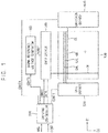
- FIG. 1 is a block diagram illustrating a display apparatus according to an example embodiment of the present inventive concept.
- the display apparatus includes a display panel 100 and a display panel driver.
- the display panel driver includes a driving controller 200, a gate driver 300, a gamma reference voltage generator 400, a data driver 500 and an emission driver 600.
- the display panel 100 has a display region on which an image is displayed and a peripheral region adjacent to the display region.
- the display panel 100 includes a plurality of gate lines GWL, GIL and GBL, a plurality of data lines DL, a plurality of emission lines EL and a plurality of pixels electrically connected to the gate lines GWL, GIL and GBL, the data lines DL and the emission lines EL.
- the gate lines GWL, GIL and GBL extend in a first direction D1
- the data lines DL extend in a second direction D2 crossing the first direction D1
- the emission lines EL extend in the first direction D1.
- the driving controller 200 receives input image data IMG and an input control signal CONT from an external apparatus (not shown).
- the input image data IMG may include red image data, green image data and blue image data.
- the input image data IMG may include white image data.
- the input image data IMG may include magenta image data, cyan image data and yellow image data.
- the input control signal CONT may include a master clock signal and a data enable signal.
- the input control signal CONT may further include a vertical synchronizing signal and a horizontal synchronizing signal.
- the driving controller 200 generates a first control signal CONT1, a second control signal CONT2, a third control signal CONT3, a fourth control signal CONT4 and a data signal DATA based on the input image data IMG and the input control signal CONT.
- the driving controller 200 generates the first control signal CONT1 for controlling an operation of the gate driver 300 based on the input control signal CONT, and outputs the first control signal CONT1 to the gate driver 300.
- the first control signal CONT1 may include a vertical start signal and a gate clock signal.
- the driving controller 200 generates the second control signal CONT2 for controlling an operation of the data driver 500 based on the input control signal CONT, and outputs the second control signal CONT2 to the data driver 500.
- the second control signal CONT2 may include a horizontal start signal and a load signal.
- the driving controller 200 generates the data signal DATA based on the input image data IMG.
- the driving controller 200 outputs the data signal DATA to the data driver 500.
- the driving controller 200 generates the third control signal CONT3 for controlling an operation of the gamma reference voltage generator 400 based on the input control signal CONT, and outputs the third control signal CONT3 to the gamma reference voltage generator 400.
- the driving controller 200 generates the fourth control signal CONT4 for controlling an operation of the emission driver 600 based on the input control signal CONT, and outputs the fourth control signal CONT4 to the emission driver 600.
- the gate driver 300 generates gate signals driving the gate lines GWL, GIL and GBL in response to the first control signal CONT1 received from the driving controller 200.
- the gate driver 300 may sequentially output the gate signals to the gate lines GWL, GIL and GBL.
- the gamma reference voltage generator 400 generates a gamma reference voltage VGREF in response to the third control signal CONT3 received from the driving controller 200.
- the gamma reference voltage generator 400 provides the gamma reference voltage VGREF to the data driver 500.
- the gamma reference voltage VGREF has a value corresponding to a level of the data signal DATA.
- the gamma reference voltage generator 400 may be disposed in the driving controller 200, or in the data driver 500.
- the data driver 500 receives the second control signal CONT2 and the data signal DATA from the driving controller 200, and receives the gamma reference voltages VGREF from the gamma reference voltage generator 400.
- the data driver 500 converts the data signal DATA into data voltages having an analog type using the gamma reference voltages VGREF.
- the data driver 500 outputs the data voltages to the data lines DL.
- the data driver 500 may be integratedly formed with the driving controller 200 so that the data driver 500 and the driving controller 200 may form a timing controller embedded data driver TED.
- the emission driver 600 generates emission signals to drive the emission lines EL in response to the fourth control signal CONT4 received from the driving controller 200.
- the emission driver 600 may output the emission signals to the emission lines EL.
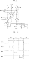
- FIG. 2 is a circuit diagram illustrating a pixel of the display panel 100 of FIG. 1 .
- FIG. 3 is a timing diagram illustrating input signals applied to the pixel of FIG. 2 .
- the display panel 100 includes the plurality of the pixels.
- Each pixel includes an organic light emitting diode OLED.
- the pixels receive a data write gate signal GW, a data initialization gate signal GI, an organic light emitting diode initialization signal GB, the data voltage VDATA and the emission signal EM and the organic light emitting diodes OLED of the pixels emit light corresponding to the level of the data voltage VDATA to display the image.
- At least one of the pixels may include a driving switching element T1, a data initializer T4-1 and T4-2, a data writer T2, T3-1 and T3-2, an organic light emitting element OLED, an organic light emitting element initializer T7-1 and T7-2 and a light emitting controller T5 and T6.
- the pixel may further include a storage capacitor CST and a stabilization capacitor CL.
- the data initializer T4-1 and T4-2 initializes a voltage at a control electrode N1 of the driving switching element T1 to a first initialization voltage VINT1.
- the data initializer T4-1 and T4-2 may include a control electrode receiving the data initialization gate signal GI, an input electrode receiving the first initialization voltage VINT1 and an output electrode connected to the control electrode N1 of the driving switching element T1.
- the data initializer T4-1 and T4-2 may include a (4-1)-th switching element T4-1 and a (4-2)-th switching element T4-2 which are connected to each other in series.
- the (4-1)-th switching element T4-1 may include a control electrode receiving the data initialization gate signal GI, an input electrode connected to an output electrode N5 of the (4-2)-th switching element T4-2 and an output electrode connected to the control electrode N1 of the driving switching element T1.
- the (4-2)-th switching element may include a control electrode receiving the data initialization gate signal GI, an input electrode receiving the first initialization voltage VINT1 and the output electrode connected to the input electrode of the (4-1)-th switching element T4-1.
- the data initializer T4-1 and T4-2 includes the (4-1)-th switching element T4-1 and the (4-2)-th switching element T4-2 which are connected to each other in series, a current leakage due to a high voltage applied to both ends of the data initializer T4-1 and T4-2 may be prevented.
- the data writer T2, T3-1 and T3-2 may write a data voltage to the control electrode N1 of the driving switching element T1 based on a data write gate signal GW.
- the data writer T2, T3-1 and T3-2 may include a first data writer T2 including a control electrode receiving the data write gate signal GW, an input electrode receiving the data voltage VDATA and an output electrode connected to an input electrode N2 of the driving switching element T1.
- the data writer T2, T3-1 and T3-2 may further include a second data writer T3-1 and T3-2 including a control electrode receiving the data write gate signal GW, an input electrode connected to an output electrode N3 of the driving switching element T1 and an output electrode connected to the control electrode N1 of the driving switching element T1.
- the second data writer T3-1 and T3-2 may include a (3-1)-th switching element T3-1 and a (3-2)-th switching element T3-2 which are connected to each other in series.
- the (3-1)-th switching element T3-1 may include a control electrode receiving the data write gate signal GW, an input electrode connected to an output electrode N4 of the (3-2)-th switching element T3-2 and an output electrode connected to the control electrode N1 of the driving switching element T1.
- the (3-2)-th switching element may include a control electrode receiving the data write gate signal GW, an input electrode connected to the output electrode N3 of the driving switching element T1 and the output electrode connected to the input electrode of the (3-1)-th switching element T3-1.
- the second data writer T3-1 and T3-2 includes the (3-1)-th switching element T3-1 and the (3-2)-th switching element T3-2 which are connected to each other in series, a current leakage due to a high voltage applied to both ends of the second data writer T3-1 and T3-2 may be prevented.
- the organic light emitting element initializer T7-1 and T7-2 initializes an anode electrode of the organic light emitting element to a second initialization voltage VINT2 based on the organic light emitting diode initialization signal GB.
- an absolute value of the second initialization voltage VINT2 may be greater than an absolute value of the first initialization voltage VINT1.
- an absolute value of a second power voltage ELVSS, the absolute value of the initialization voltage and an absolute value of a low level VGL of the gate signal increase, a drain-source voltage VDS of the (3-1)-th switching element T3-1, the (3-2)-th switching element T3-2, the (4-1)-th switching element T4-1 and the (4-2)-th switching element T4-2 may increase so that the leakage may occur.
- the first initialization voltage VINT1 and the second initialization voltage VINT2 may be set differently.
- the organic light emitting element initializer T7-1 and T7-2 may include a (7-1)-th switching element T7-1 and a (7-2)-th switching element T7-2 which are connected to each other in series.
- the (7-1)-th switching element T7-1 may include a control electrode receiving the organic light emitting element initialization gate signal GB, an input electrode connected to an output electrode of the (7-2)-th switching element T7-2 and an output electrode connected to the anode electrode of the organic light emitting element OLED.
- the (7-2)-th switching element may include a control electrode receiving the organic light emitting element initialization gate signal GB, an input electrode receiving the second initialization voltage VINT2 and the output electrode connected to the input electrode of the (7-1)-th switching element T7-1.
- the light emitting controller T5 and T6 controls a light emission of the organic light emitting element OLED based on the emission signal EM.
- the light emitting controller T5 and T6 may include a first light emitting controller T5 including a control electrode receiving the emission signal EM, an input electrode receiving a first power voltage ELVDD the and an output electrode connected to the input electrode N2 of the driving switching element T1.
- the light emitting controller T5 and T6 may further include a second light emitting controller T6 including a control electrode receiving the emission signal EM, an input electrode connected to the output electrode N3 of the driving switching element T1 and an output electrode connected to the anode electrode of the organic light emitting element OLED.
- a second light emitting controller T6 including a control electrode receiving the emission signal EM, an input electrode connected to the output electrode N3 of the driving switching element T1 and an output electrode connected to the anode electrode of the organic light emitting element OLED.
- the storage capacitor CST includes a first electrode receiving the first power voltage ELVDD and a second electrode connected to the control electrode N1 of the driving switching element T1.
- the stabilization capacitor CL includes a first electrode receiving the first power voltage ELVDD and a second electrode connected to the input electrode of the (3-1)-th switching element T3-1.
- the voltage at the input electrode of the (3-1)-th switching element T3-1 is stabilized by the stabilization capacitor CL so that the current leakage through the (3-1)-th switching element T3-1 and the (3-2)-th switching element T3-2 may be reduced.
- the second electrode of the stabilization capacitor CL may be also connected to the input electrode of the (4-1)-th switching element T4-1.
- the voltage at the input electrode of the (4-1)-th switching element T4-1 is stabilized by the stabilization capacitor CL so that the current leakage through the (4-1)-th switching element T4-1 and the (4-2)-th switching element T4-2 may be reduced.
- the organic light emitting element OLED includes the anode electrode and a cathode electrode receiving the second power voltage ELVSS.
- the first node N1 and the storage capacitor CST are initialized in response to the data initialization gate signal GI.
- of the first switching element T1 is compensated and the data voltage VDATA of which the threshold voltage
- the anode electrode of the organic light emitting diode OLED is initialized in response to the organic light emitting diode initialization gate signal GB.
- the organic light emitting diode OLED emit the light in response to the emission signal EM so that the pixel displays the image.
- the off duration of the emission signal EM corresponds to first to third durations DU1, DU2 and DU3 in the present example embodiment, the present inventive concept may not be limited thereto.
- the off duration of the emission signal EM may include the data write duration DU2 and the off duration of the emission signal EM may be longer than the first to third durations DU1, DU2 and DU3.
- the data initialization gate signal GI may have an active level.
- the active level of the data initialization gate signal GI may be a low level.
- the (4-1)-th switching element T4-1 and the (4-2)-th switching element T4-2 are turned on so that the first initialization voltage VINT1 may be applied to the first node N1.
- the data write gate signal GW may have an active level.
- the active level of the data write gate signal GW may be a low level.
- a second switching element T2 and the (3-1)-th switching element T3-1 and the (3-2)-th switching element T3-2 are turned on.
- the first switching element T1 is turned on in response to the first initialization voltage VINT1.
- of the threshold voltage of the first switching element T1 from the data voltage VDATA may be charged at the first node N1 along a path generated by the first, second, (3-1)-th and (3-2)-th switching elements T1, T2, T3-1 and T3-2.
- the organic light emitting diode initialization signal GB may have an active level.
- the active level of the organic light emitting diode initialization signal GB may be a low level.
- the (7-1)-th switching element T7-1 and the (7-2)-th switching element T7-2 are turned on so that the second initialization voltage VINT2 may be applied to the anode electrode of the organic light emitting diode OLED.
- the emission signal EM may have an active level.
- the active level of the emission signal EM may be a low level.
- the fifth switching element T5 and the sixth switching element T6 are turned on.
- the first switching element T1 is turned on by the data voltage VDATA.
- a driving current flows through the fifth switching element T5, the first switching element T1 and the sixth switching element T6 to drive the organic light emitting diode OLED.
- An intensity of the driving current may be determined by the level of the data voltage VDATA.
- a luminance of the organic light emitting diode OLED is determined by the intensity of the driving current.
- is compensated during the second duration DU2, so that the driving current may be determined regardless of the threshold voltage
- FIG. 4 is a cross-sectional view illustrating a portion of an organic light emitting element initialization switching element T7-1 and T7-2 of FIG. 2 .
- FIG. 5 is a graph illustrating a shift of a threshold voltage of the organic light emitting element initialization switching element T7-1 and T7-2 of FIG. 2 .
- the (7-1)-th switching element T7-1 and the (7-2)-th switching element T7-2 may include a polyimide layer PI, a barrier layer BR disposed on the polyimide layer PI, a conductive layer ML disposed on the barrier layer BR, a buffer layer BF covering the conductive layer ML, a P+ layer disposed on the buffer layer BR, an active layer AL disposed between the buffer layer BF and the P+ layer, a gate insulation layer GI covering the P+ layer and the active layer AL and a control electrode G disposed on the gate insulation layer GI.
- the first to (7-2)-th switching elements T1, T2, T3-1, T3-2, T4-1, T4-2, T5, T6, T7-1 and T7-2 may include a control electrode G, an input electrode, an output electrode and a conductive layer ML facing the control electrode G.
- the same control signal may be applied to the control electrode G and the conductive layer ML of the first to sixth switching elements T1, T2, T3-1, T3-2, T4-1, T4-2, T5 and T6.
- different control signals may be applied to the control electrode G and the conductive layer ML of the (7-1)-th switching element T7-1 and the (7-2)-th switching element T7-2.
- the (7-1)-th switching element T7-1 and the (7-2)-th switching element T7-2 includes a control electrode G receiving the organic light emitting diode initialization signal GB, an input electrode receiving the second initialization voltage VINT2, an output electrode connected to the anode electrode of the light organic light emitting element OLED and the conductive layer ML facing the control electrode G and receiving a compensation control signal different from the organic light emitting diode initialization signal GB.
- the compensation control signal may be the first initialization voltage VINT1.
- the second initialization voltage VINT2 is -14.1V and the first initialization voltage VINT 1 is -3.5V.
- the first initialization voltage VINT1 and the second initialization voltage VINT2 are less than 0 and an absolute value of the first initialization voltage VINT1 may be less than the second initialization voltage VINT2.
- the compensation control signal VINT1 is applied to the conductive layers ML of the (7-1)-th switching element T7-1 and the (7-2)-th switching element T7-2 so that threshold voltages Vth of the (7-1)-th switching element T7-1 and the (7-2)-th switching element T7-2 may be shifted in a positive direction.
- C1 represents a current voltage curve of the (7-1)-th switching element T7-1 and the (7-2)-th switching element T7-2 when the organic light emitting diode initialization signal GB is applied to the conductive layer ML of the (7-1)-th switching element T7-1 and the (7-2)-th switching element T7-2.
- C2 represents a current voltage curve of the (7-1)-th switching element T7-1 and the (7-2)-th switching element T7-2 when the compensation control signal VINT1 is applied to the conductive layer ML of the (7-1)-th switching element T7-1 and the (7-2)-th switching element T7-2.
- the threshold voltage Vth of the (7-1)-th switching element T7-1 and the (7-2)-th switching element T7-2 is shifted in the positive direction so that the driving voltage (e.g. the absolute value of the low level VGL of the gate signal) of the display apparatus may be reduced. Accordingly, the power consumption of the display apparatus may be reduced. In addition, the driving voltage (e.g. the absolute value of the low level VGL of the gate signal) of the display apparatus is reduced so that a reliability of the gate driver 300 may be enhanced.
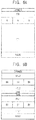
- FIG. 6A is a cross-sectional view illustrating an example of an organic light emitting element of FIG. 2 .
- FIG. 6B is a cross-sectional view illustrating an example of an organic light emitting element of FIG. 2 .
- the organic light emitting element OLED may include a single light emitting layer R, G and B.
- the organic light emitting element OLED may include two light emitting layers R1, G1, B1, R2, G2 and B2 to enhance a reliability and a lifetime.
- the organic light emitting element OLED may include the anode electrode ANODE, a hole transport layer HTL disposed on the anode electrode ANODE, the light emitting layer R, G and B disposed on the hole transport layer HTL, an electron transport layer ETL disposed on the light emitting layer R, G and B and a cathode electrode CATHODE disposed on the electron transport layer ETL.
- the organic light emitting element OLED may include the anode electrode ANODE, a first light emitting layer R1, G1 and B1 disposed on the anode electrode ANODE, a second light emitting layer R2, G2 and B2 disposed on the first light emitting layer R1, G1 and B1 and a cathode layer CATHODE disposed on the second light emitting layer R2, G2 and B2.
- the organic light emitting element OLED may further include the anode electrode ANODE, a first hole transport layer HTL1 disposed between the anode electrode ANODE and the first light emitting layer R1, G1 and B1, a first electron transport layer ETL1 disposed on the first light emitting layer R1, G1 and B1, a n-type charge generation layer nCGL disposed on the first electron transport layer ETL1, a p-type charge generation layer pCGL disposed on the n-type charge generation layer nCGL, a second hole transport layer HTL2 disposed between the p-type charge generation layer pCGL and the second light emitting layer R2, G2 and B2 and a second electron transport layer ETL2 disposed between the second light emitting layer R2, G2 and B2 and the cathode electrode CATHODE.
- the driving voltage of the display apparatus may be further increased.
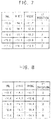
- FIG. 7 is a table illustrating voltages at nodes of an organic light emitting element and an organic light emitting element initialization switching element according to a comparative embodiment.
- FIG. 8 is a table illustrating voltages at nodes of the organic light emitting element and the organic light emitting element initialization switching element of FIG. 2 .
- the organic light emitting diode initialization signal GB is applied to the control electrode G and the conductive layer ML of the (7-1)-th switching element T7-1 and the (7-2)-th switching element T7-2.
- the organic light emitting diode initialization signal GB is applied to the control electrode G of the (7-1)-th switching element T7-1 and the (7-2)-th switching element T7-2 and the compensation control signal VINT1 is applied to the conductive layer ML of the (7-1)-th switching element T7-1 and the (7-2)-th switching element T7-2.
- the second initialization voltage VINT2 and the second power voltage ELVSS may be -14.1V.
- a single switching element T7 is illustrated instead of the (7-1)-th switching element T7-1 and the (7-2)-th switching element T7-2 for convenience of explanation.
- the gate source voltage VGS of a seventh switching element T7 is less than a threshold voltage of the seventh switching element T7 so that the seventh switching element T7 does not normally operate.
- the gate source voltage VGS of a seventh switching element T7 is less than the threshold voltage of the seventh switching element T7 so that the seventh switching element T7 does not normally operate.
- the gate source voltage VGS of the seventh switching element T7 reaches the threshold voltage of the seventh switching element T7 so that the seventh switching element T7 may normally operate.
- the pixel normally operates when the low level VGL of the gate signal (e.g. GI, GB and GW) is equal to or less than -17.6V.
- the low level VGL of the gate signal e.g. GI, GB and GW
- the compensation control signal VINT1 is applied to the conductive layer ML so that the threshold voltage of the seventh switching element T7 may be shifted in the positive direction by 1.5V to 2V as shown in FIG. 5 .
- the gate source voltage VGS of the seventh switching element T7 is less than a threshold voltage of the seventh switching element T7 so that the seventh switching element T7 does not normally operate.
- the gate source voltage VGS of a seventh switching element T7 is less than the threshold voltage of the seventh switching element T7 so that the seventh switching element T7 does not normally operate.
- the gate source voltage VGS of the seventh switching element T7 reaches the threshold voltage of the seventh switching element T7 so that the seventh switching element T7 may normally operate.
- the pixel normally operates when the low level VGL of the gate signal (e.g. GI, GB and GW) is equal to or less than -15.6V so that the absolute value of the driving voltage VGL may decrease by 2V compared to the case of FIG. 7 .
- the driving voltage VGL is decreased, the power consumption of the display apparatus may be reduced.
- the reliability of the gate driver 300 may be enhanced.
- the signal VINT1 different from the signal GB applied to the control electrode G of the organic light emitting element initialization switching element T7-1 and T7-2 is applied to the conductive layer ML facing the control electrode G of the organic light emitting element initialization switching element T7-1 and T7-2 so that the threshold voltage of the organic light emitting element initialization switching element T7-1 and T7-2 may be decreased.
- the power consumption of the display apparatus may be reduced and the reliability of the gate driver 300 may be enhanced.
- FIG. 9 is a circuit diagram illustrating a pixel of a display panel according to an example embodiment of the present inventive concept.
- the display apparatus according to the present example embodiment is substantially the same as the display apparatus of the previous example embodiment explained referring to FIGS. 1 to 8 except for the signal applied to the control electrode of the (7-1)-th switching element and the (7-2)-th switching element.
- the same reference numerals will be used to refer to the same or like parts as those described in the previous example embodiment of FIGS. 1 to 8 and any repetitive explanation concerning the above elements will be omitted.
- the display apparatus includes a display panel 100 and a display panel driver.
- the display panel driver includes a driving controller 200, a gate driver 300, a gamma reference voltage generator 400, a data driver 500 and an emission driver 600.
- At least one of the pixels may include a driving switching element T1, a data initializer T4-1 and T4-2, a data writer T2, T3-1 and T3-2, an organic light emitting element OLED, an organic light emitting element initializer T7-1 and T7-2 and a light emitting controller T5 and T6.
- the pixel may further include a storage capacitor CST and a stabilization capacitor CL.
- the organic light emitting element initializer T7-1 and T7-2 initializes an anode electrode of the organic light emitting element to a second initialization voltage VINT2 based on the organic light emitting diode initialization signal GB.
- the first to (7-2)-th switching elements T1, T2, T3-1, T3-2, T4-1, T4-2, T5, T6, T7-1 and T7-2 may include a control electrode G, an input electrode, an output electrode and a conductive layer ML facing the control electrode G.
- the same control signal may be applied to the control electrode G and the conductive layer ML of the first to sixth switching elements T1, T2, T3-1, T3-2, T4-1, T4-2, T5 and T6.
- different control signals may be applied to the control electrode G and the conductive layer ML of the (7-1)-th switching element T7-1 and the (7-2)-th switching element T7-2.
- a compensation control signal VX may be independently formed from other driving signals.
- the (7-1)-th switching element T7-1 and the (7-2)-th switching element T7-2 may be p-type switching elements so that the compensation control signal VX may be applied in a positive direction.
- the (7-1)-th switching element T7-1 and the (7-2)-th switching element T7-2 may be n-type switching elements so that the compensation control signal VX may be applied in a negative direction.
- a shift range of the threshold voltage Vth of the (7-1)-th switching element T7-1 and the (7-2)-th switching element T7-2 may be greater than 0V and less than 10V.
- the signal VX different from the signal GB applied to the control electrode G of the organic light emitting element initialization switching element T7-1 and T7-2 is applied to the conductive layer ML facing the control electrode G of the organic light emitting element initialization switching element T7-1 and T7-2 so that the threshold voltage of the organic light emitting element initialization switching element T7-1 and T7-2 may be decreased.
- the power consumption of the display apparatus may be reduced and the reliability of the gate driver 300 may be enhanced.
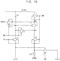
- FIG. 10 is a circuit diagram illustrating a pixel of a display panel according to an example embodiment of the present inventive concept.
- the display apparatus according to the present example embodiment is substantially the same as the display apparatus of the previous example embodiment explained referring to FIGS. 1 to 8 except for the pixel circuit.
- the same reference numerals will be used to refer to the same or like parts as those described in the previous example embodiment of FIGS. 1 to 8 and any repetitive explanation concerning the above elements will be omitted.
- the display apparatus includes a display panel 100 and a display panel driver.
- the display panel driver includes a driving controller 200, a gate driver 300, a gamma reference voltage generator 400, a data driver 500 and an emission driver 600.
- At least one of the pixels may include a driving switching element T1, a data initializer T4, a data writer T2 and T3, an organic light emitting element OLED, an organic light emitting element initializer T7 and a light emitting controller T5 and T6.
- the pixel may further include a storage capacitor CST and a stabilization capacitor CL.
- the second data writer T3 may include a single switching element T3 unlike FIG. 2 .
- the data initializer T4 may include a single switching element T4 unlike FIG. 2 .
- the organic light emitting element initializer T7 may include a single switching element T7 unlike FIG. 2 .
- the organic light emitting element initializer T7 initializes an anode electrode of the organic light emitting element to a second initialization voltage VINT2 based on the organic light emitting diode initialization signal GB.
- the first to seventh switching elements T1 to T7 may include a control electrode G, an input electrode, an output electrode and a conductive layer ML facing the control electrode G.
- the same control signal may be applied to the control electrode G and the conductive layer ML of the first to sixth switching elements T1 to T6.
- the compensation control signal may be the first initialization voltage VINT1.
- the compensation control signal may be independently generated from other driving signals as explained referring to FIG. 9 .
- the signal VINT1 different from the signal GB applied to the control electrode G of the organic light emitting element initialization switching element T7 is applied to the conductive layer ML facing the control electrode G of the organic light emitting element initialization switching element T7 so that the threshold voltage of the organic light emitting element initialization switching element T7 may be decreased.
- the power consumption of the display apparatus may be reduced and the reliability of the gate driver 300 may be enhanced.
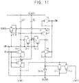
- FIG. 11 is a circuit diagram illustrating a pixel of a display panel according to an example embodiment of the present inventive concept.
- the display apparatus according to the present example embodiment is substantially the same as the display apparatus of the previous example embodiment explained referring to FIGS. 1 to 8 except for the signal applied to the control electrode of the (7-1)-th switching element and the (7-2)-th switching element.
- the same reference numerals will be used to refer to the same or like parts as those described in the previous example embodiment of FIGS. 1 to 8 and any repetitive explanation concerning the above elements will be omitted.
- the display apparatus includes a display panel 100 and a display panel driver.
- the display panel driver includes a driving controller 200, a gate driver 300, a gamma reference voltage generator 400, a data driver 500 and an emission driver 600.
- At least one of the pixels may include a driving switching element T1, a data initializer T4-1 and T4-2, a data writer T2, T3-1 and T3-2, an organic light emitting element OLED, an organic light emitting element initializer T7-1 and T7-2 and a light emitting controller T5 and T6.
- the pixel may further include a storage capacitor CST and a stabilization capacitor CL.
- the organic light emitting element initializer T7-1 and T7-2 initializes an anode electrode of the organic light emitting element to a second initialization voltage VINT2 based on the organic light emitting diode initialization signal GB.
- the organic light emitting diode initialization signal GB may have a phase same as a phase of the data write gate signal GW.
- the data write gate signal GW may be directly applied to the control electrode G of the organic light emitting element initializer T7-1 and T7-2.
- the first to (7-2)-th switching elements T1, T2, T3-1, T3-2, T4-1, T4-2, T5, T6, T7-1 and T7-2 may include a control electrode G, an input electrode, an output electrode and a conductive layer ML facing the control electrode G.
- the same control signal may be applied to the control electrode G and the conductive layer ML of the first to sixth switching elements T1, T2, T3-1, T3-2, T4-1, T4-2, T5 and T6.
- different control signals may be applied to the control electrode G and the conductive layer ML of the (7-1)-th switching element T7-1 and the (7-2)-th switching element T7-2.
- the compensation control signal may be the first initialization voltage VINT1.
- the compensation control signal may be independently generated from other driving signals as explained referring to FIG. 9 .
- the signal VINT1 different from the signal GB applied to the control electrode G of the organic light emitting element initialization switching element T7-1 and T7-2 is applied to the conductive layer ML facing the control electrode G of the organic light emitting element initialization switching element T7-1 and T7-2 so that the threshold voltage of the organic light emitting element initialization switching element T7-1 and T7-2 may be decreased.
- the power consumption of the display apparatus may be reduced and the reliability of the gate driver 300 may be enhanced.
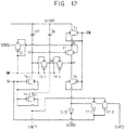
- FIG. 12 is a circuit diagram illustrating a pixel of a display panel according to an example embodiment of the present inventive concept.
- the display apparatus according to the present example embodiment is substantially the same as the display apparatus of the previous example embodiment explained referring to FIGS. 1 to 8 except for the signal applied to the control electrode of the (7-1)-th switching element and the (7-2)-th switching element.
- the same reference numerals will be used to refer to the same or like parts as those described in the previous example embodiment of FIGS. 1 to 8 and any repetitive explanation concerning the above elements will be omitted.
- the display apparatus includes a display panel 100 and a display panel driver.
- the display panel driver includes a driving controller 200, a gate driver 300, a gamma reference voltage generator 400, a data driver 500 and an emission driver 600.
- At least one of the pixels may include a driving switching element T1, a data initializer T4-1 and T4-2, a data writer T2, T3-1 and T3-2, an organic light emitting element OLED, an organic light emitting element initializer T7-1 and T7-2 and a light emitting controller T5 and T6.
- the pixel may further include a storage capacitor CST and a stabilization capacitor CL.
- the organic light emitting element initializer T7-1 and T7-2 initializes an anode electrode of the organic light emitting element to a second initialization voltage VINT2 based on the organic light emitting diode initialization signal GB.
- the organic light emitting diode initialization signal GB may have a phase same as a phase of the data initialization gate signal GI.
- the data initialization gate signal GI may be directly applied to the control electrode G of the organic light emitting element initializer T7-1 and T7-2.
- the first to (7-2)-th switching elements T1, T2, T3-1, T3-2, T4-1, T4-2, T5, T6, T7-1 and T7-2 may include a control electrode G, an input electrode, an output electrode and a conductive layer ML facing the control electrode G.
- the same control signal may be applied to the control electrode G and the conductive layer ML of the first to sixth switching elements T1, T2, T3-1, T3-2, T4-1, T4-2, T5 and T6.
- different control signals may be applied to the control electrode G and the conductive layer ML of the (7-1)-th switching element T7-1 and the (7-2)-th switching element T7-2.
- the compensation control signal may be the first initialization voltage VINT1.
- the compensation control signal may be independently generated from other driving signals as explained referring to FIG. 9 .
- the signal VINT1 different from the signal GB applied to the control electrode G of the organic light emitting element initialization switching element T7-1 and T7-2 is applied to the conductive layer ML facing the control electrode G of the organic light emitting element initialization switching element T7-1 and T7-2 so that the threshold voltage of the organic light emitting element initialization switching element T7-1 and T7-2 may be decreased.
- the power consumption of the display apparatus may be reduced and the reliability of the gate driver 300 may be enhanced.
- the reliability may be enhanced and the power consumption may be reduced due to the decrease of the driving voltage.
Landscapes
- Engineering & Computer Science (AREA)
- Physics & Mathematics (AREA)
- Optics & Photonics (AREA)
- Computer Hardware Design (AREA)
- General Physics & Mathematics (AREA)
- Theoretical Computer Science (AREA)
- Microelectronics & Electronic Packaging (AREA)
- Control Of Indicators Other Than Cathode Ray Tubes (AREA)
- Electroluminescent Light Sources (AREA)
- Control Of El Displays (AREA)
Abstract
Description
- Example embodiments of the present inventive concept relate to a pixel circuit and a display apparatus including the pixel circuit. More particularly, example embodiments of the present inventive concept relate to a pixel circuit enhancing a reliability and reducing a power consumption due to a decrease of a driving voltage and a display apparatus including the pixel circuit.
- Generally, a display apparatus includes a display panel and a display panel driver. The display panel includes a plurality of gate lines, a plurality of data lines, a plurality of emission lines and a plurality of pixels. The display panel driver includes a gate driver, a data driver, an emission driver and a driving controller. The gate driver outputs gate signals to the gate lines. The data driver outputs data voltages to the data lines. The emission driver outputs emission signals to the emission lines. The driving controller controls the gate driver, the data driver and the emission driver.
- For high luminance driving, an absolute value of a power voltage, an absolute value of an initialization voltage and an absolute value of a gate low level voltage may need to increase. Due to the increase of the absolute value of the power voltage, the absolute value of the initialization voltage and the absolute value of the gate low level voltage, the power consumption of the display apparatus may increase and reliabilities of a switching element of a driving circuit and a switching element of a pixel may be reduced.
- Example embodiments of the present inventive concept provide a pixel circuit capable of enhancing a reliability and reducing a power consumption due to a decrease of a driving voltage.
- Example embodiments of the present inventive concept also provide a display apparatus including the pixel circuit.
- In an example embodiment of a pixel circuit according to the present inventive concept, the pixel circuit includes a driving switching element, a data initializer, a data writer, an organic light emitting element, an organic light emitting element initializer and a light emitting controller. The data initializer is configured to initialize a voltage of a control electrode of the driving switching element to a first initialization voltage based on a data initialization gate signal. The data writer is configured to write a data voltage to the control electrode of the driving switching element based on a data write gate signal. The organic light emitting element initializer is configured to initialize an anode electrode of the organic light emitting element to a second initialization voltage based on an organic light emitting element initialization gate signal. The light emitting controller is configured to control an emission of the organic light emitting element based on an emission signal. The organic light emitting element initializer includes a control electrode configured to receive the organic light emitting element initialization gate signal, an input electrode configured to receive the second initialization voltage, an output electrode connected to the anode electrode and a conductive layer facing the control electrode of the organic light emitting element initializer and configured to receive a compensation control signal different from the organic light emitting element initialization gate signal.
- In an example embodiment, the compensation control signal may be the first initialization voltage.
- In an example embodiment, the data initializer may include a control electrode configured to receive the data initialization gate signal, an input electrode configured to receive the first initialization voltage and an output electrode connected to the control electrode of the driving switching element.
- In an example embodiment, the data writer may include a first data writer comprising a control electrode configured to receive the data write gate signal, an input electrode configured to receive the data voltage and an output electrode connected to an input electrode of the driving switching element.
- In an example embodiment, the data writer may further include a second data writer comprising a control electrode configured to receive the data write gate signal, an input electrode connected to an output electrode of the driving switching element and an output electrode connected to the control electrode of the driving switching element.
- In an example embodiment, the second data writer may include a (3-1)-th switching element and a (3-2)-th switching element which are connected in series. The (3-1)-th switching element may include a control electrode configured to receive the data write gate signal, an input electrode connected to an output electrode of the (3-2)-th switching element and an output electrode connected to the control electrode of the driving switching element. The (3-2)-th switching element may include a control electrode configured to receive the data write gate signal, an input electrode connected to the output electrode of the driving switching element and an output electrode connected to the input electrode of the (3-1)-th switching element.
- In an example embodiment, the pixel circuit may further include a stabilization capacitor comprising a first electrode configured to receive a first power voltage and a second electrode connected to the input electrode of the (3-1)-th switching element.
- In an example embodiment, the data initializer may include a (4-1)-th switching element and a (4-2)-th switching element which are connected in series. The (4-1)-th switching element may include a control electrode configured to receive the data initialization gate signal, an input electrode connected to an output electrode of the (4-2)-th switching element and an output electrode connected to the control electrode of the driving switching element. The (4-2)-th switching element may include a control electrode configured to receive the data initialization gate signal, an input electrode configured to receive the first initialization voltage and an output electrode connected to the input electrode of the (4-1)-th switching element.
- In an example embodiment, the input electrode of the (4-1)-th switching element may be connected to the input electrode of the (3-1)-th switching element.
- In an example embodiment, the pixel circuit may further include a storage capacitor comprising a first electrode configured to receive a first power voltage and a second electrode connected to the control electrode of the driving switching element.
- In an example embodiment, the organic light emitting element initializer may include a (7-1)-th switching element and a (7-2)-th switching element which are connected in series. The (7-1)-th switching element may include a control electrode configured to receive the organic light emitting element initialization gate signal, an input electrode connected to an output electrode of the (7-2)-th switching element and an output electrode connected to the anode electrode of the organic light emitting element. The (7-2)-th switching element may include a control electrode configured to receive the organic light emitting element initialization gate signal, an input electrode configured to receive the second initialization voltage and an output electrode connected to the input electrode of the (7-1)-th switching element.
- In an example embodiment, the light emitting controller may include a first light emitting controller comprising a control electrode configured to receive the emission signal, an input electrode configured to receive a first power voltage and an output electrode connected to an input electrode of the driving switching element.
- In an example embodiment, the light emitting controller may further include a second light emitting controller comprising a control electrode configured to receive the emission signal, an input electrode connected to an output electrode of the driving switching element and an output electrode connected to the anode electrode of the organic light emitting element.
- In an example embodiment, the organic light emitting element may include the anode electrode, a first light emitting layer disposed on the anode electrode, a second light emitting layer disposed on the first light emitting layer and a cathode electrode disposed on the second light emitting layer.
- In an example embodiment, the organic light emitting element may further include a first hole transport layer disposed between the anode electrode and the first light emitting layer, a first electron transport layer disposed on the first light emitting layer, a n-type charge generation layer disposed on the first electron transport layer, a p-type charge generation layer disposed on the n-type charge generation layer, a second hole transport layer disposed between the p-type charge generation layer and the second light emitting layer and a second electron transport layer disposed between the second light emitting layer and the cathode electrode.
- In an example embodiment, the organic light emitting element initialization gate signal may have a phase same as a phase of the data write gate signal.
- In an example embodiment, the organic light emitting element initialization gate signal may have a phase same as a phase of the data initialization gate signal.
- In an example embodiment of a display apparatus according to the present inventive concept, the display apparatus includes a display panel, a gate driver, a data driver and an emission driver. The display panel includes a plurality of pixels. The gate driver is configured to output a gate signal to the display panel. The data driver is configured to output a data voltage to the display panel. The emission driver is configured to output an emission signal to the display panel. At least one of the pixels includes a driving switching element, a data initializer, a data writer, an organic light emitting element, an organic light emitting element initializer and a light emitting controller. The data initializer is configured to initialize a voltage of a control electrode of the driving switching element to a first initialization voltage based on a data initialization gate signal. The data writer is configured to write a data voltage to the control electrode of the driving switching element based on a data write gate signal. The organic light emitting element initializer is configured to initialize an anode electrode of the organic light emitting element to a second initialization voltage based on an organic light emitting element initialization gate signal. The light emitting controller is configured to control an emission of the organic light emitting element based on an emission signal. The organic light emitting element initializer includes a control electrode configured to receive the organic light emitting element initialization gate signal, an input electrode configured to receive the second initialization voltage, an output electrode connected to the anode electrode and a conductive layer facing the control electrode of the organic light emitting element initializer and configured to receive a compensation control signal different from the organic light emitting element initialization gate signal.
- In an example embodiment, the compensation control signal may be the first initialization voltage.
- According to the pixel circuit and the display apparatus including the pixel circuit, the signal different from the signal applied to the control electrode of the organic light emitting element initialization switching element is applied to the conductive layer facing the control electrode of the organic light emitting element initialization switching element so that the threshold voltage of the organic light emitting element initialization switching element may be decreased.
- The threshold voltage of the organic light emitting element initialization switching element is decreased so that the driving voltage of the display apparatus may be decreased. Thus, a power consumption of the display apparatus may be reduced.
- In addition, the threshold voltage of the organic light emitting element initialization switching element is decreased so that the reliability of the switching element of the driving circuit of the display apparatus and the reliability of the switching element of the pixel may be enhanced.
-
-
FIG. 1 is a block diagram illustrating a display apparatus according to an example embodiment of the present inventive concept. -
FIG. 2 is a circuit diagram illustrating a pixel of a display panel ofFIG. 1 . -
FIG. 3 is a timing diagram illustrating input signals applied to the pixel ofFIG. 2 . -
FIG. 4 is a cross-sectional view illustrating a portion of an organic light emitting element initialization switching element ofFIG. 2 . -
FIG. 5 is a graph illustrating a shift of a threshold voltage of the organic light emitting element initialization switching element ofFIG. 2 . -
FIG. 6A is a cross-sectional view illustrating an example of an organic light emitting element ofFIG. 2 . -
FIG. 6B is a cross-sectional view illustrating an example of an organic light emitting element ofFIG. 2 . -
FIG. 7 is a table illustrating voltages at nodes of an organic light emitting element and an organic light emitting element initialization switching element according to a comparative embodiment. -
FIG. 8 is a table illustrating voltages at nodes of the organic light emitting element and the organic light emitting element initialization switching element ofFIG. 2 . -
FIG. 9 is a circuit diagram illustrating a pixel of a display panel according to an example embodiment of the present inventive concept. -
FIG. 10 is a circuit diagram illustrating a pixel of a display panel according to an example embodiment of the present inventive concept. -
FIG. 11 is a circuit diagram illustrating a pixel of a display panel according to an example embodiment of the present inventive concept. -
FIG. 12 is a circuit diagram illustrating a pixel of a display panel according to an example embodiment of the present inventive concept. - Hereinafter, the present inventive concept will be explained in detail with reference to the accompanying drawings.
-
FIG. 1 is a block diagram illustrating a display apparatus according to an example embodiment of the present inventive concept. - Referring to
FIG. 1 , the display apparatus includes adisplay panel 100 and a display panel driver. The display panel driver includes a drivingcontroller 200, agate driver 300, a gammareference voltage generator 400, adata driver 500 and anemission driver 600. - The
display panel 100 has a display region on which an image is displayed and a peripheral region adjacent to the display region. - The
display panel 100 includes a plurality of gate lines GWL, GIL and GBL, a plurality of data lines DL, a plurality of emission lines EL and a plurality of pixels electrically connected to the gate lines GWL, GIL and GBL, the data lines DL and the emission lines EL. The gate lines GWL, GIL and GBL extend in a first direction D1, the data lines DL extend in a second direction D2 crossing the first direction D1 and the emission lines EL extend in the first direction D1. - The driving
controller 200 receives input image data IMG and an input control signal CONT from an external apparatus (not shown). For example, the input image data IMG may include red image data, green image data and blue image data. The input image data IMG may include white image data. The input image data IMG may include magenta image data, cyan image data and yellow image data. The input control signal CONT may include a master clock signal and a data enable signal. The input control signal CONT may further include a vertical synchronizing signal and a horizontal synchronizing signal. - The driving
controller 200 generates a first control signal CONT1, a second control signal CONT2, a third control signal CONT3, a fourth control signal CONT4 and a data signal DATA based on the input image data IMG and the input control signal CONT. - The driving
controller 200 generates the first control signal CONT1 for controlling an operation of thegate driver 300 based on the input control signal CONT, and outputs the first control signal CONT1 to thegate driver 300. The first control signal CONT1 may include a vertical start signal and a gate clock signal. - The driving
controller 200 generates the second control signal CONT2 for controlling an operation of thedata driver 500 based on the input control signal CONT, and outputs the second control signal CONT2 to thedata driver 500. The second control signal CONT2 may include a horizontal start signal and a load signal. - The driving
controller 200 generates the data signal DATA based on the input image data IMG. The drivingcontroller 200 outputs the data signal DATA to thedata driver 500. - The driving
controller 200 generates the third control signal CONT3 for controlling an operation of the gammareference voltage generator 400 based on the input control signal CONT, and outputs the third control signal CONT3 to the gammareference voltage generator 400. - The driving
controller 200 generates the fourth control signal CONT4 for controlling an operation of theemission driver 600 based on the input control signal CONT, and outputs the fourth control signal CONT4 to theemission driver 600. - The
gate driver 300 generates gate signals driving the gate lines GWL, GIL and GBL in response to the first control signal CONT1 received from the drivingcontroller 200. Thegate driver 300 may sequentially output the gate signals to the gate lines GWL, GIL and GBL. - The gamma
reference voltage generator 400 generates a gamma reference voltage VGREF in response to the third control signal CONT3 received from the drivingcontroller 200. The gammareference voltage generator 400 provides the gamma reference voltage VGREF to thedata driver 500. The gamma reference voltage VGREF has a value corresponding to a level of the data signal DATA. - In an example embodiment, the gamma
reference voltage generator 400 may be disposed in the drivingcontroller 200, or in thedata driver 500. - The
data driver 500 receives the second control signal CONT2 and the data signal DATA from the drivingcontroller 200, and receives the gamma reference voltages VGREF from the gammareference voltage generator 400. Thedata driver 500 converts the data signal DATA into data voltages having an analog type using the gamma reference voltages VGREF. Thedata driver 500 outputs the data voltages to the data lines DL. - For example, the
data driver 500 may be integratedly formed with the drivingcontroller 200 so that thedata driver 500 and the drivingcontroller 200 may form a timing controller embedded data driver TED. - The
emission driver 600 generates emission signals to drive the emission lines EL in response to the fourth control signal CONT4 received from the drivingcontroller 200. Theemission driver 600 may output the emission signals to the emission lines EL. -
FIG. 2 is a circuit diagram illustrating a pixel of thedisplay panel 100 ofFIG. 1 .FIG. 3 is a timing diagram illustrating input signals applied to the pixel ofFIG. 2 . - Referring to
FIGS. 1 to 3 , thedisplay panel 100 includes the plurality of the pixels. Each pixel includes an organic light emitting diode OLED. - The pixels receive a data write gate signal GW, a data initialization gate signal GI, an organic light emitting diode initialization signal GB, the data voltage VDATA and the emission signal EM and the organic light emitting diodes OLED of the pixels emit light corresponding to the level of the data voltage VDATA to display the image.
- At least one of the pixels may include a driving switching element T1, a data initializer T4-1 and T4-2, a data writer T2, T3-1 and T3-2, an organic light emitting element OLED, an organic light emitting element initializer T7-1 and T7-2 and a light emitting controller T5 and T6. The pixel may further include a storage capacitor CST and a stabilization capacitor CL.
- The data initializer T4-1 and T4-2 initializes a voltage at a control electrode N1 of the driving switching element T1 to a first initialization voltage VINT1.
- The data initializer T4-1 and T4-2 may include a control electrode receiving the data initialization gate signal GI, an input electrode receiving the first initialization voltage VINT1 and an output electrode connected to the control electrode N1 of the driving switching element T1.
- For example, the data initializer T4-1 and T4-2 may include a (4-1)-th switching element T4-1 and a (4-2)-th switching element T4-2 which are connected to each other in series. The (4-1)-th switching element T4-1 may include a control electrode receiving the data initialization gate signal GI, an input electrode connected to an output electrode N5 of the (4-2)-th switching element T4-2 and an output electrode connected to the control electrode N1 of the driving switching element T1. The (4-2)-th switching element may include a control electrode receiving the data initialization gate signal GI, an input electrode receiving the first initialization voltage VINT1 and the output electrode connected to the input electrode of the (4-1)-th switching element T4-1.
- When the data initializer T4-1 and T4-2 includes the (4-1)-th switching element T4-1 and the (4-2)-th switching element T4-2 which are connected to each other in series, a current leakage due to a high voltage applied to both ends of the data initializer T4-1 and T4-2 may be prevented.
- The data writer T2, T3-1 and T3-2 may write a data voltage to the control electrode N1 of the driving switching element T1 based on a data write gate signal GW.
- The data writer T2, T3-1 and T3-2 may include a first data writer T2 including a control electrode receiving the data write gate signal GW, an input electrode receiving the data voltage VDATA and an output electrode connected to an input electrode N2 of the driving switching element T1.
- In addition, the data writer T2, T3-1 and T3-2 may further include a second data writer T3-1 and T3-2 including a control electrode receiving the data write gate signal GW, an input electrode connected to an output electrode N3 of the driving switching element T1 and an output electrode connected to the control electrode N1 of the driving switching element T1.
- For example, the second data writer T3-1 and T3-2 may include a (3-1)-th switching element T3-1 and a (3-2)-th switching element T3-2 which are connected to each other in series. The (3-1)-th switching element T3-1 may include a control electrode receiving the data write gate signal GW, an input electrode connected to an output electrode N4 of the (3-2)-th switching element T3-2 and an output electrode connected to the control electrode N1 of the driving switching element T1. The (3-2)-th switching element may include a control electrode receiving the data write gate signal GW, an input electrode connected to the output electrode N3 of the driving switching element T1 and the output electrode connected to the input electrode of the (3-1)-th switching element T3-1.
- When the second data writer T3-1 and T3-2 includes the (3-1)-th switching element T3-1 and the (3-2)-th switching element T3-2 which are connected to each other in series, a current leakage due to a high voltage applied to both ends of the second data writer T3-1 and T3-2 may be prevented.
- The organic light emitting element initializer T7-1 and T7-2 initializes an anode electrode of the organic light emitting element to a second initialization voltage VINT2 based on the organic light emitting diode initialization signal GB.
- For example, an absolute value of the second initialization voltage VINT2 may be greater than an absolute value of the first initialization voltage VINT1. For high luminance driving, an absolute value of a second power voltage ELVSS, the absolute value of the initialization voltage and an absolute value of a low level VGL of the gate signal increase, a drain-source voltage VDS of the (3-1)-th switching element T3-1, the (3-2)-th switching element T3-2, the (4-1)-th switching element T4-1 and the (4-2)-th switching element T4-2 may increase so that the leakage may occur. Thus, the first initialization voltage VINT1 and the second initialization voltage VINT2 may be set differently.
- The organic light emitting element initializer T7-1 and T7-2 may include a (7-1)-th switching element T7-1 and a (7-2)-th switching element T7-2 which are connected to each other in series. The (7-1)-th switching element T7-1 may include a control electrode receiving the organic light emitting element initialization gate signal GB, an input electrode connected to an output electrode of the (7-2)-th switching element T7-2 and an output electrode connected to the anode electrode of the organic light emitting element OLED. The (7-2)-th switching element may include a control electrode receiving the organic light emitting element initialization gate signal GB, an input electrode receiving the second initialization voltage VINT2 and the output electrode connected to the input electrode of the (7-1)-th switching element T7-1.
- The light emitting controller T5 and T6 controls a light emission of the organic light emitting element OLED based on the emission signal EM.
- The light emitting controller T5 and T6 may include a first light emitting controller T5 including a control electrode receiving the emission signal EM, an input electrode receiving a first power voltage ELVDD the and an output electrode connected to the input electrode N2 of the driving switching element T1.
- The light emitting controller T5 and T6 may further include a second light emitting controller T6 including a control electrode receiving the emission signal EM, an input electrode connected to the output electrode N3 of the driving switching element T1 and an output electrode connected to the anode electrode of the organic light emitting element OLED.
- The storage capacitor CST includes a first electrode receiving the first power voltage ELVDD and a second electrode connected to the control electrode N1 of the driving switching element T1.
- The stabilization capacitor CL includes a first electrode receiving the first power voltage ELVDD and a second electrode connected to the input electrode of the (3-1)-th switching element T3-1. The voltage at the input electrode of the (3-1)-th switching element T3-1 is stabilized by the stabilization capacitor CL so that the current leakage through the (3-1)-th switching element T3-1 and the (3-2)-th switching element T3-2 may be reduced.
- The second electrode of the stabilization capacitor CL may be also connected to the input electrode of the (4-1)-th switching element T4-1. The voltage at the input electrode of the (4-1)-th switching element T4-1 is stabilized by the stabilization capacitor CL so that the current leakage through the (4-1)-th switching element T4-1 and the (4-2)-th switching element T4-2 may be reduced.
- The organic light emitting element OLED includes the anode electrode and a cathode electrode receiving the second power voltage ELVSS.
- In
FIG. 3 , during a first duration DU1, the first node N1 and the storage capacitor CST are initialized in response to the data initialization gate signal GI. During a second duration DU2, a threshold voltage |VTH| of the first switching element T1 is compensated and the data voltage VDATA of which the threshold voltage |VTH| is compensated is written to the first node N1 in response to the data write gate signal GW. During a third duration DU3, the anode electrode of the organic light emitting diode OLED is initialized in response to the organic light emitting diode initialization gate signal GB. During a fourth duration DU4, the organic light emitting diode OLED emit the light in response to the emission signal EM so that the pixel displays the image. - Although the off duration of the emission signal EM corresponds to first to third durations DU1, DU2 and DU3 in the present example embodiment, the present inventive concept may not be limited thereto. When the off duration of the emission signal EM may include the data write duration DU2 and the off duration of the emission signal EM may be longer than the first to third durations DU1, DU2 and DU3.
- During the first duration DU1, the data initialization gate signal GI may have an active level. For example, the active level of the data initialization gate signal GI may be a low level. When the data initialization gate signal GI has the active level, the (4-1)-th switching element T4-1 and the (4-2)-th switching element T4-2 are turned on so that the first initialization voltage VINT1 may be applied to the first node N1.
- During the second duration DU2, the data write gate signal GW may have an active level. For example, the active level of the data write gate signal GW may be a low level. When the data write gate signal GW has the active level, a second switching element T2 and the (3-1)-th switching element T3-1 and the (3-2)-th switching element T3-2 are turned on. In addition, the first switching element T1 is turned on in response to the first initialization voltage VINT1.
- A voltage which is subtraction an absolute value |VTH| of the threshold voltage of the first switching element T1 from the data voltage VDATA may be charged at the first node N1 along a path generated by the first, second, (3-1)-th and (3-2)-th switching elements T1, T2, T3-1 and T3-2.
- During the third duration DU3, the organic light emitting diode initialization signal GB may have an active level. For example, the active level of the organic light emitting diode initialization signal GB may be a low level. When the organic light emitting diode initialization signal GB has the active level, the (7-1)-th switching element T7-1 and the (7-2)-th switching element T7-2 are turned on so that the second initialization voltage VINT2 may be applied to the anode electrode of the organic light emitting diode OLED.
- During the fourth duration DU4, the emission signal EM may have an active level. The active level of the emission signal EM may be a low level. When the emission signal EM has the active level, the fifth switching element T5 and the sixth switching element T6 are turned on. In addition, the first switching element T1 is turned on by the data voltage VDATA.
- A driving current flows through the fifth switching element T5, the first switching element T1 and the sixth switching element T6 to drive the organic light emitting diode OLED. An intensity of the driving current may be determined by the level of the data voltage VDATA. A luminance of the organic light emitting diode OLED is determined by the intensity of the driving current.
- The threshold voltage |VTH| is compensated during the second duration DU2, so that the driving current may be determined regardless of the threshold voltage |VTH| of the first switching element T1 when the organic light emitting diode OLED emits the light during the fourth duration DU4.
-
FIG. 4 is a cross-sectional view illustrating a portion of an organic light emitting element initialization switching element T7-1 and T7-2 ofFIG. 2 .FIG. 5 is a graph illustrating a shift of a threshold voltage of the organic light emitting element initialization switching element T7-1 and T7-2 ofFIG. 2 . - Referring to
FIGS. 1 to 5 , the (7-1)-th switching element T7-1 and the (7-2)-th switching element T7-2 may include a polyimide layer PI, a barrier layer BR disposed on the polyimide layer PI, a conductive layer ML disposed on the barrier layer BR, a buffer layer BF covering the conductive layer ML, a P+ layer disposed on the buffer layer BR, an active layer AL disposed between the buffer layer BF and the P+ layer, a gate insulation layer GI covering the P+ layer and the active layer AL and a control electrode G disposed on the gate insulation layer GI. - In the present example embodiment, the first to (7-2)-th switching elements T1, T2, T3-1, T3-2, T4-1, T4-2, T5, T6, T7-1 and T7-2 may include a control electrode G, an input electrode, an output electrode and a conductive layer ML facing the control electrode G.
- The same control signal may be applied to the control electrode G and the conductive layer ML of the first to sixth switching elements T1, T2, T3-1, T3-2, T4-1, T4-2, T5 and T6.
- Unlike the first to sixth switching elements T1, T2, T3-1, T3-2, T4-1, T4-2, T5 and T6, different control signals may be applied to the control electrode G and the conductive layer ML of the (7-1)-th switching element T7-1 and the (7-2)-th switching element T7-2.
- For example, the (7-1)-th switching element T7-1 and the (7-2)-th switching element T7-2 includes a control electrode G receiving the organic light emitting diode initialization signal GB, an input electrode receiving the second initialization voltage VINT2, an output electrode connected to the anode electrode of the light organic light emitting element OLED and the conductive layer ML facing the control electrode G and receiving a compensation control signal different from the organic light emitting diode initialization signal GB.
- In the present example embodiment, the compensation control signal may be the first initialization voltage VINT1. For example, the second initialization voltage VINT2 is -14.1V and the first initialization voltage VINT 1 is -3.5V. For example, the first initialization voltage VINT1 and the second initialization voltage VINT2 are less than 0 and an absolute value of the first initialization voltage VINT1 may be less than the second initialization voltage VINT2.
- Thus, the compensation control signal VINT1 is applied to the conductive layers ML of the (7-1)-th switching element T7-1 and the (7-2)-th switching element T7-2 so that threshold voltages Vth of the (7-1)-th switching element T7-1 and the (7-2)-th switching element T7-2 may be shifted in a positive direction.
- In
FIG. 5 , C1 represents a current voltage curve of the (7-1)-th switching element T7-1 and the (7-2)-th switching element T7-2 when the organic light emitting diode initialization signal GB is applied to the conductive layer ML of the (7-1)-th switching element T7-1 and the (7-2)-th switching element T7-2. C2 represents a current voltage curve of the (7-1)-th switching element T7-1 and the (7-2)-th switching element T7-2 when the compensation control signal VINT1 is applied to the conductive layer ML of the (7-1)-th switching element T7-1 and the (7-2)-th switching element T7-2. - The threshold voltage Vth of the (7-1)-th switching element T7-1 and the (7-2)-th switching element T7-2 is shifted in the positive direction so that the driving voltage (e.g. the absolute value of the low level VGL of the gate signal) of the display apparatus may be reduced. Accordingly, the power consumption of the display apparatus may be reduced. In addition, the driving voltage (e.g. the absolute value of the low level VGL of the gate signal) of the display apparatus is reduced so that a reliability of the
gate driver 300 may be enhanced. -
FIG. 6A is a cross-sectional view illustrating an example of an organic light emitting element ofFIG. 2 .FIG. 6B is a cross-sectional view illustrating an example of an organic light emitting element ofFIG. 2 . - In
FIG. 6A , for example, the organic light emitting element OLED may include a single light emitting layer R, G and B. InFIG. 6B , for example, the organic light emitting element OLED may include two light emitting layers R1, G1, B1, R2, G2 and B2 to enhance a reliability and a lifetime. - Referring to
FIG. 6A , the organic light emitting element OLED may include the anode electrode ANODE, a hole transport layer HTL disposed on the anode electrode ANODE, the light emitting layer R, G and B disposed on the hole transport layer HTL, an electron transport layer ETL disposed on the light emitting layer R, G and B and a cathode electrode CATHODE disposed on the electron transport layer ETL. - Referring to
FIG. 6B , the organic light emitting element OLED may include the anode electrode ANODE, a first light emitting layer R1, G1 and B1 disposed on the anode electrode ANODE, a second light emitting layer R2, G2 and B2 disposed on the first light emitting layer R1, G1 and B1 and a cathode layer CATHODE disposed on the second light emitting layer R2, G2 and B2. - For example, the organic light emitting element OLED may further include the anode electrode ANODE, a first hole transport layer HTL1 disposed between the anode electrode ANODE and the first light emitting layer R1, G1 and B1, a first electron transport layer ETL1 disposed on the first light emitting layer R1, G1 and B1, a n-type charge generation layer nCGL disposed on the first electron transport layer ETL1, a p-type charge generation layer pCGL disposed on the n-type charge generation layer nCGL, a second hole transport layer HTL2 disposed between the p-type charge generation layer pCGL and the second light emitting layer R2, G2 and B2 and a second electron transport layer ETL2 disposed between the second light emitting layer R2, G2 and B2 and the cathode electrode CATHODE.
- When the display apparatus includes the organic light emitting element OLED including the first and second light emitting layers R1, G1, B1, R2, G2 and B2, the driving voltage of the display apparatus may be further increased.
-
FIG. 7 is a table illustrating voltages at nodes of an organic light emitting element and an organic light emitting element initialization switching element according to a comparative embodiment.FIG. 8 is a table illustrating voltages at nodes of the organic light emitting element and the organic light emitting element initialization switching element ofFIG. 2 . - In
FIG. 7 , for example, the organic light emitting diode initialization signal GB is applied to the control electrode G and the conductive layer ML of the (7-1)-th switching element T7-1 and the (7-2)-th switching element T7-2. InFIG. 8 , for example, the organic light emitting diode initialization signal GB is applied to the control electrode G of the (7-1)-th switching element T7-1 and the (7-2)-th switching element T7-2 and the compensation control signal VINT1 is applied to the conductive layer ML of the (7-1)-th switching element T7-1 and the (7-2)-th switching element T7-2. InFIGS. 7 and 8 , for example, the second initialization voltage VINT2 and the second power voltage ELVSS may be -14.1V. InFIGS. 7 and 8 , a single switching element T7 is illustrated instead of the (7-1)-th switching element T7-1 and the (7-2)-th switching element T7-2 for convenience of explanation. - In
FIG. 7 , when the low level VGL of the gate signal (e.g. GI, GB and GW) is -13.6V, the anode voltage is -11.7V. Herein, the gate source voltage VGS of a seventh switching element T7 is less than a threshold voltage of the seventh switching element T7 so that the seventh switching element T7 does not normally operate. When the low level VGL of the gate signal (e.g. GI, GB and GW) is -14.6V, the anode voltage is -12.3V. Herein, the gate source voltage VGS of a seventh switching element T7 is less than the threshold voltage of the seventh switching element T7 so that the seventh switching element T7 does not normally operate. - When the low level VGL of the gate signal (e.g. GI, GB and GW) is -17.6V, the anode voltage is -14.1V. Herein, the gate source voltage VGS of the seventh switching element T7 reaches the threshold voltage of the seventh switching element T7 so that the seventh switching element T7 may normally operate.
- In the case of
FIG. 7 , the pixel normally operates when the low level VGL of the gate signal (e.g. GI, GB and GW) is equal to or less than -17.6V. - In
FIG. 8 , for example, the compensation control signal VINT1 is applied to the conductive layer ML so that the threshold voltage of the seventh switching element T7 may be shifted in the positive direction by 1.5V to 2V as shown inFIG. 5 . - In
FIG. 8 , when the low level VGL of the gate signal (e.g. GI, GB and GW) is -13.6V, the anode voltage is -12.7V. Herein, the gate source voltage VGS of the seventh switching element T7 is less than a threshold voltage of the seventh switching element T7 so that the seventh switching element T7 does not normally operate. When the low level VGL of the gate signal (e.g. GI, GB and GW) is -14.6V, the anode voltage is -13.3V. Herein, the gate source voltage VGS of a seventh switching element T7 is less than the threshold voltage of the seventh switching element T7 so that the seventh switching element T7 does not normally operate. - When the low level VGL of the gate signal (e.g. GI, GB and GW) is -15.6V, the anode voltage is -14.1V. Herein, the gate source voltage VGS of the seventh switching element T7 reaches the threshold voltage of the seventh switching element T7 so that the seventh switching element T7 may normally operate.
- In the case of
FIG. 8 , the pixel normally operates when the low level VGL of the gate signal (e.g. GI, GB and GW) is equal to or less than -15.6V so that the absolute value of the driving voltage VGL may decrease by 2V compared to the case ofFIG. 7 . When the driving voltage VGL is decreased, the power consumption of the display apparatus may be reduced. In addition, when the driving voltage VGL is decreased, the reliability of thegate driver 300 may be enhanced. - According to the present example embodiment, the signal VINT1 different from the signal GB applied to the control electrode G of the organic light emitting element initialization switching element T7-1 and T7-2 is applied to the conductive layer ML facing the control electrode G of the organic light emitting element initialization switching element T7-1 and T7-2 so that the threshold voltage of the organic light emitting element initialization switching element T7-1 and T7-2 may be decreased.
- Thus, the power consumption of the display apparatus may be reduced and the reliability of the
gate driver 300 may be enhanced. -
FIG. 9 is a circuit diagram illustrating a pixel of a display panel according to an example embodiment of the present inventive concept. - The display apparatus according to the present example embodiment is substantially the same as the display apparatus of the previous example embodiment explained referring to
FIGS. 1 to 8 except for the signal applied to the control electrode of the (7-1)-th switching element and the (7-2)-th switching element. Thus, the same reference numerals will be used to refer to the same or like parts as those described in the previous example embodiment ofFIGS. 1 to 8 and any repetitive explanation concerning the above elements will be omitted. - Referring to
FIGS. 1 and3 to 9 , the display apparatus includes adisplay panel 100 and a display panel driver. The display panel driver includes a drivingcontroller 200, agate driver 300, a gammareference voltage generator 400, adata driver 500 and anemission driver 600. - At least one of the pixels may include a driving switching element T1, a data initializer T4-1 and T4-2, a data writer T2, T3-1 and T3-2, an organic light emitting element OLED, an organic light emitting element initializer T7-1 and T7-2 and a light emitting controller T5 and T6. The pixel may further include a storage capacitor CST and a stabilization capacitor CL.
- The organic light emitting element initializer T7-1 and T7-2 initializes an anode electrode of the organic light emitting element to a second initialization voltage VINT2 based on the organic light emitting diode initialization signal GB.
- In the present example embodiment, the first to (7-2)-th switching elements T1, T2, T3-1, T3-2, T4-1, T4-2, T5, T6, T7-1 and T7-2 may include a control electrode G, an input electrode, an output electrode and a conductive layer ML facing the control electrode G.
- The same control signal may be applied to the control electrode G and the conductive layer ML of the first to sixth switching elements T1, T2, T3-1, T3-2, T4-1, T4-2, T5 and T6.
- Unlike the first to sixth switching elements T1, T2, T3-1, T3-2, T4-1, T4-2, T5 and T6, different control signals may be applied to the control electrode G and the conductive layer ML of the (7-1)-th switching element T7-1 and the (7-2)-th switching element T7-2.
- In the present example embodiment, a compensation control signal VX may be independently formed from other driving signals. The (7-1)-th switching element T7-1 and the (7-2)-th switching element T7-2 may be p-type switching elements so that the compensation control signal VX may be applied in a positive direction. Alternatively, the (7-1)-th switching element T7-1 and the (7-2)-th switching element T7-2 may be n-type switching elements so that the compensation control signal VX may be applied in a negative direction.
- For example, a shift range of the threshold voltage Vth of the (7-1)-th switching element T7-1 and the (7-2)-th switching element T7-2 may be greater than 0V and less than 10V.
- According to the present example embodiment, the signal VX different from the signal GB applied to the control electrode G of the organic light emitting element initialization switching element T7-1 and T7-2 is applied to the conductive layer ML facing the control electrode G of the organic light emitting element initialization switching element T7-1 and T7-2 so that the threshold voltage of the organic light emitting element initialization switching element T7-1 and T7-2 may be decreased.
- Thus, the power consumption of the display apparatus may be reduced and the reliability of the
gate driver 300 may be enhanced. -
FIG. 10 is a circuit diagram illustrating a pixel of a display panel according to an example embodiment of the present inventive concept. - The display apparatus according to the present example embodiment is substantially the same as the display apparatus of the previous example embodiment explained referring to
FIGS. 1 to 8 except for the pixel circuit. Thus, the same reference numerals will be used to refer to the same or like parts as those described in the previous example embodiment ofFIGS. 1 to 8 and any repetitive explanation concerning the above elements will be omitted. - Referring to
FIGS. 1 ,3 to 8 and10 , the display apparatus includes adisplay panel 100 and a display panel driver. The display panel driver includes a drivingcontroller 200, agate driver 300, a gammareference voltage generator 400, adata driver 500 and anemission driver 600. - At least one of the pixels may include a driving switching element T1, a data initializer T4, a data writer T2 and T3, an organic light emitting element OLED, an organic light emitting element initializer T7 and a light emitting controller T5 and T6. The pixel may further include a storage capacitor CST and a stabilization capacitor CL.
- In the present example embodiment, the second data writer T3 may include a single switching element T3 unlike
FIG. 2 . - In the present example embodiment, the data initializer T4 may include a single switching element T4 unlike
FIG. 2 . - In the present example embodiment, the organic light emitting element initializer T7 may include a single switching element T7 unlike
FIG. 2 . - The organic light emitting element initializer T7 initializes an anode electrode of the organic light emitting element to a second initialization voltage VINT2 based on the organic light emitting diode initialization signal GB.
- In the present example embodiment, the first to seventh switching elements T1 to T7 may include a control electrode G, an input electrode, an output electrode and a conductive layer ML facing the control electrode G.
- The same control signal may be applied to the control electrode G and the conductive layer ML of the first to sixth switching elements T1 to T6.
- Unlike the first to sixth switching elements T1 to T6, different control signals may be applied to the control electrode G and the conductive layer ML of the seventh switching element T7.
- In the present example embodiment, the compensation control signal may be the first initialization voltage VINT1. Alternatively, the compensation control signal may be independently generated from other driving signals as explained referring to
FIG. 9 . - According to the present example embodiment, the signal VINT1 different from the signal GB applied to the control electrode G of the organic light emitting element initialization switching element T7 is applied to the conductive layer ML facing the control electrode G of the organic light emitting element initialization switching element T7 so that the threshold voltage of the organic light emitting element initialization switching element T7 may be decreased.
- Thus, the power consumption of the display apparatus may be reduced and the reliability of the
gate driver 300 may be enhanced. -
FIG. 11 is a circuit diagram illustrating a pixel of a display panel according to an example embodiment of the present inventive concept. - The display apparatus according to the present example embodiment is substantially the same as the display apparatus of the previous example embodiment explained referring to
FIGS. 1 to 8 except for the signal applied to the control electrode of the (7-1)-th switching element and the (7-2)-th switching element. Thus, the same reference numerals will be used to refer to the same or like parts as those described in the previous example embodiment ofFIGS. 1 to 8 and any repetitive explanation concerning the above elements will be omitted. - Referring to
FIGS. 1 ,3 to 8 and11 , the display apparatus includes adisplay panel 100 and a display panel driver. The display panel driver includes a drivingcontroller 200, agate driver 300, a gammareference voltage generator 400, adata driver 500 and anemission driver 600. - At least one of the pixels may include a driving switching element T1, a data initializer T4-1 and T4-2, a data writer T2, T3-1 and T3-2, an organic light emitting element OLED, an organic light emitting element initializer T7-1 and T7-2 and a light emitting controller T5 and T6. The pixel may further include a storage capacitor CST and a stabilization capacitor CL.
- The organic light emitting element initializer T7-1 and T7-2 initializes an anode electrode of the organic light emitting element to a second initialization voltage VINT2 based on the organic light emitting diode initialization signal GB.
- In the present example embodiment, the organic light emitting diode initialization signal GB may have a phase same as a phase of the data write gate signal GW. For example, the data write gate signal GW may be directly applied to the control electrode G of the organic light emitting element initializer T7-1 and T7-2.
- In the present example embodiment, the first to (7-2)-th switching elements T1, T2, T3-1, T3-2, T4-1, T4-2, T5, T6, T7-1 and T7-2 may include a control electrode G, an input electrode, an output electrode and a conductive layer ML facing the control electrode G.
- The same control signal may be applied to the control electrode G and the conductive layer ML of the first to sixth switching elements T1, T2, T3-1, T3-2, T4-1, T4-2, T5 and T6.
- Unlike the first to sixth switching elements T1, T2, T3-1, T3-2, T4-1, T4-2, T5 and T6, different control signals may be applied to the control electrode G and the conductive layer ML of the (7-1)-th switching element T7-1 and the (7-2)-th switching element T7-2.
- In the present example embodiment, the compensation control signal may be the first initialization voltage VINT1. Alternatively, the compensation control signal may be independently generated from other driving signals as explained referring to
FIG. 9 . - According to the present example embodiment, the signal VINT1 different from the signal GB applied to the control electrode G of the organic light emitting element initialization switching element T7-1 and T7-2 is applied to the conductive layer ML facing the control electrode G of the organic light emitting element initialization switching element T7-1 and T7-2 so that the threshold voltage of the organic light emitting element initialization switching element T7-1 and T7-2 may be decreased.
- Thus, the power consumption of the display apparatus may be reduced and the reliability of the
gate driver 300 may be enhanced. -
FIG. 12 is a circuit diagram illustrating a pixel of a display panel according to an example embodiment of the present inventive concept. - The display apparatus according to the present example embodiment is substantially the same as the display apparatus of the previous example embodiment explained referring to
FIGS. 1 to 8 except for the signal applied to the control electrode of the (7-1)-th switching element and the (7-2)-th switching element. Thus, the same reference numerals will be used to refer to the same or like parts as those described in the previous example embodiment ofFIGS. 1 to 8 and any repetitive explanation concerning the above elements will be omitted. - Referring to
FIGS. 1 ,3 to 8 and12 , the display apparatus includes adisplay panel 100 and a display panel driver. The display panel driver includes a drivingcontroller 200, agate driver 300, a gammareference voltage generator 400, adata driver 500 and anemission driver 600. - At least one of the pixels may include a driving switching element T1, a data initializer T4-1 and T4-2, a data writer T2, T3-1 and T3-2, an organic light emitting element OLED, an organic light emitting element initializer T7-1 and T7-2 and a light emitting controller T5 and T6. The pixel may further include a storage capacitor CST and a stabilization capacitor CL.
- The organic light emitting element initializer T7-1 and T7-2 initializes an anode electrode of the organic light emitting element to a second initialization voltage VINT2 based on the organic light emitting diode initialization signal GB.
- In the present example embodiment, the organic light emitting diode initialization signal GB may have a phase same as a phase of the data initialization gate signal GI. For example, the data initialization gate signal GI may be directly applied to the control electrode G of the organic light emitting element initializer T7-1 and T7-2.
- In the present example embodiment, the first to (7-2)-th switching elements T1, T2, T3-1, T3-2, T4-1, T4-2, T5, T6, T7-1 and T7-2 may include a control electrode G, an input electrode, an output electrode and a conductive layer ML facing the control electrode G.
- The same control signal may be applied to the control electrode G and the conductive layer ML of the first to sixth switching elements T1, T2, T3-1, T3-2, T4-1, T4-2, T5 and T6.
- Unlike the first to sixth switching elements T1, T2, T3-1, T3-2, T4-1, T4-2, T5 and T6, different control signals may be applied to the control electrode G and the conductive layer ML of the (7-1)-th switching element T7-1 and the (7-2)-th switching element T7-2.
- In the present example embodiment, the compensation control signal may be the first initialization voltage VINT1. Alternatively, the compensation control signal may be independently generated from other driving signals as explained referring to
FIG. 9 . - According to the present example embodiment, the signal VINT1 different from the signal GB applied to the control electrode G of the organic light emitting element initialization switching element T7-1 and T7-2 is applied to the conductive layer ML facing the control electrode G of the organic light emitting element initialization switching element T7-1 and T7-2 so that the threshold voltage of the organic light emitting element initialization switching element T7-1 and T7-2 may be decreased.
- Thus, the power consumption of the display apparatus may be reduced and the reliability of the
gate driver 300 may be enhanced. - According to the pixel circuit and the display apparatus of the present inventive concept as explained above, the reliability may be enhanced and the power consumption may be reduced due to the decrease of the driving voltage.
- Although a few example embodiments of the present inventive concept have been described, those skilled in the art will readily appreciate that many modifications are possible in the example embodiments without materially departing from the novel teachings and advantages of the present inventive concept. Accordingly, all such modifications are intended to be included within the scope of the present inventive concept as defined in the claims.
<EXPLANATION OF REFERENCE NUMERALS> 100: display panel 200: driving controller 300: gate driver 400: gamma reference voltage generator 500: data driver 600: emission driver
Claims (19)
- A pixel circuit comprising:a driving switching element;a data initializer configured to initialize a voltage of a control electrode of the driving switching element to a first initialization voltage based on a data initialization gate signal;a data writer configured to write a data voltage to the control electrode of the driving switching element based on a data write gate signal;an organic light emitting element;an organic light emitting element initializer configured to initialize an anode electrode of the organic light emitting element to a second initialization voltage based on an organic light emitting element initialization gate signal; anda light emitting controller configured to control an emission of the organic light emitting element based on an emission signal,wherein the organic light emitting element initializer comprises a control electrode configured to receive the organic light emitting element initialization gate signal, an input electrode configured to receive the second initialization voltage, an output electrode connected to the anode electrode and a conductive layer facing the control electrode of the organic light emitting element initializer and configured to receive a compensation control signal different from the organic light emitting element initialization gate signal.
- The pixel circuit of claim 1, wherein the compensation control signal is the first initialization voltage.
- The pixel circuit of claim 1, wherein the data initializer comprises a control electrode configured to receive the data initialization gate signal, an input electrode configured to receive the first initialization voltage and an output electrode connected to the control electrode of the driving switching element.
- The pixel circuit of claim 1, wherein the data writer comprises a first data writer comprising a control electrode configured to receive the data write gate signal, an input electrode configured to receive the data voltage and an output electrode connected to an input electrode of the driving switching element.
- The pixel circuit of claim 4, wherein the data writer further comprises a second data writer comprising a control electrode configured to receive the data write gate signal, an input electrode connected to an output electrode of the driving switching element and an output electrode connected to the control electrode of the driving switching element.
- The pixel circuit of claim 5, wherein the second data writer comprises a (3-1)-th switching element and a (3-2)-th switching element which are connected in series,
wherein the (3-1)-th switching element comprises a control electrode configured to receive the data write gate signal, an input electrode connected to an output electrode of the (3-2)-th switching element and an output electrode connected to the control electrode of the driving switching element, and
wherein the (3-2)-th switching element comprises a control electrode configured to receive the data write gate signal, an input electrode connected to the output electrode of the driving switching element and an output electrode connected to the input electrode of the (3-1)-th switching element. - The pixel circuit of claim 6, further comprising a stabilization capacitor comprising a first electrode configured to receive a first power voltage and a second electrode connected to the input electrode of the (3-1)-th switching element.
- The pixel circuit of claim 6, wherein the data initializer comprises a (4-1)-th switching element and a (4-2)-th switching element which are connected in series,
wherein the (4-1)-th switching element comprises a control electrode configured to receive the data initialization gate signal, an input electrode connected to an output electrode of the (4-2)-th switching element and an output electrode connected to the control electrode of the driving switching element, and
wherein the (4-2)-th switching element comprises a control electrode configured to receive the data initialization gate signal, an input electrode configured to receive the first initialization voltage and an output electrode connected to the input electrode of the (4-1)-th switching element. - The pixel circuit of claim 8, wherein the input electrode of the (4-1)-th switching element is connected to the input electrode of the (3-1)-th switching element.
- The pixel circuit of claim 1, further comprising a storage capacitor comprising a first electrode configured to receive a first power voltage and a second electrode connected to the control electrode of the driving switching element.
- The pixel circuit of claim 1, wherein the organic light emitting element initializer comprises a (7-1)-th switching element and a (7-2)-th switching element which are connected in series,
wherein the (7-1)-th switching element comprises a control electrode configured to receive the organic light emitting element initialization gate signal, an input electrode connected to an output electrode of the (7-2)-th switching element and an output electrode connected to the anode electrode of the organic light emitting element, and
wherein the (7-2)-th switching element comprises a control electrode configured to receive the organic light emitting element initialization gate signal, an input electrode configured to receive the second initialization voltage and an output electrode connected to the input electrode of the (7-1)-th switching element. - The pixel circuit of claim 1, wherein the light emitting controller comprises a first light emitting controller comprising a control electrode configured to receive the emission signal, an input electrode configured to receive a first power voltage and an output electrode connected to an input electrode of the driving switching element.
- The pixel circuit of claim 12, wherein the light emitting controller further comprises a second light emitting controller comprising a control electrode configured to receive the emission signal, an input electrode connected to an output electrode of the driving switching element and an output electrode connected to the anode electrode of the organic light emitting element.
- The pixel circuit of claim 1, wherein the organic light emitting element comprises:the anode electrode;a first light emitting layer disposed on the anode electrode;a second light emitting layer disposed on the first light emitting layer; anda cathode electrode disposed on the second light emitting layer.
- The pixel circuit of claim 14, wherein the organic light emitting element further comprises:a first hole transport layer disposed between the anode electrode and the first light emitting layer;a first electron transport layer disposed on the first light emitting layer;a n-type charge generation layer disposed on the first electron transport layer;a p-type charge generation layer disposed on the n-type charge generation layer;a second hole transport layer disposed between the p-type charge generation layer and the second light emitting layer; anda second electron transport layer disposed between the second light emitting layer and the cathode electrode.
- The pixel circuit of claim 1, wherein the organic light emitting element initialization gate signal has a phase same as a phase of the data write gate signal.
- The pixel circuit of claim 1, wherein the organic light emitting element initialization gate signal has a phase same as a phase of the data initialization gate signal.
- A display apparatus comprising:a display panel comprising a plurality of pixels;a gate driver configured to output a gate signal to the display panel;a data driver configured to output a data voltage to the display panel; andan emission driver configured to output an emission signal to the display panel,wherein at least one of the pixels comprises:a driving switching element;a data initializer configured to initialize a voltage of a control electrode of the driving switching element to a first initialization voltage based on a data initialization gate signal;a data writer configured to write a data voltage to the control electrode of the driving switching element based on a data write gate signal;an organic light emitting element;an organic light emitting element initializer configured to initialize an anode electrode of the organic light emitting element to a second initialization voltage based on an organic light emitting element initialization gate signal; anda light emitting controller configured to control an emission of the organic light emitting element based on an emission signal,wherein the organic light emitting element initializer comprises a control electrode configured to receive the organic light emitting element initialization gate signal, an input electrode configured to receive the second initialization voltage, an output electrode connected to the anode electrode and a conductive layer facing the control electrode of the organic light emitting element initializer and configured to receive a compensation control signal different from the organic light emitting element initialization gate signal.
- The display apparatus of claim 18, wherein the compensation control signal is the first initialization voltage.
Applications Claiming Priority (2)
| Application Number | Priority Date | Filing Date | Title |
|---|---|---|---|
| KR1020180094530A KR102584291B1 (en) | 2018-08-13 | 2018-08-13 | Pixel circuit and display apparatus having the same |
| PCT/KR2019/007683 WO2020036307A1 (en) | 2018-08-13 | 2019-06-25 | Pixel circuit and display device including same |
Publications (3)
| Publication Number | Publication Date |
|---|---|
| EP3839931A1 true EP3839931A1 (en) | 2021-06-23 |
| EP3839931A4 EP3839931A4 (en) | 2022-05-04 |
| EP3839931B1 EP3839931B1 (en) | 2025-10-15 |
Family
ID=69525542
Family Applications (1)
| Application Number | Title | Priority Date | Filing Date |
|---|---|---|---|
| EP19849392.6A Active EP3839931B1 (en) | 2018-08-13 | 2019-06-25 | Pixel circuit and display device including same |
Country Status (5)
| Country | Link |
|---|---|
| US (1) | US11386854B2 (en) |
| EP (1) | EP3839931B1 (en) |
| KR (1) | KR102584291B1 (en) |
| CN (1) | CN112585671B (en) |
| WO (1) | WO2020036307A1 (en) |
Families Citing this family (13)
| Publication number | Priority date | Publication date | Assignee | Title |
|---|---|---|---|---|
| CN111179859B (en) * | 2020-03-16 | 2021-03-02 | 京东方科技集团股份有限公司 | Pixel circuit, display panel and display device |
| KR102847345B1 (en) | 2020-06-30 | 2025-08-18 | 삼성디스플레이 주식회사 | Pixel and organic light emitting display |
| CN112289269A (en) * | 2020-10-30 | 2021-01-29 | 合肥维信诺科技有限公司 | Pixel circuit, control method thereof and display panel |
| KR20220111820A (en) | 2021-02-02 | 2022-08-10 | 삼성디스플레이 주식회사 | Pixel and display apparatus having the same |
| KR102936739B1 (en) | 2021-04-27 | 2026-03-12 | 삼성디스플레이 주식회사 | Pixel and display apparatus having the same |
| KR102884569B1 (en) | 2021-12-09 | 2025-11-12 | 삼성디스플레이 주식회사 | Pixel circuit and display apparatus having the same |
| KR102877032B1 (en) | 2021-12-13 | 2025-10-28 | 삼성디스플레이 주식회사 | Pixel and display device including the same |
| KR102862796B1 (en) * | 2021-12-16 | 2025-09-22 | 엘지디스플레이 주식회사 | Electroluminescence Display Device |
| US12484380B2 (en) | 2021-12-24 | 2025-11-25 | Samsung Display Co., Ltd. | Display panel |
| CN114724519B (en) * | 2022-03-31 | 2023-10-20 | 昆山国显光电有限公司 | Pixel circuit, display panel and display device |
| CN118765412A (en) * | 2023-01-19 | 2024-10-11 | 京东方科技集团股份有限公司 | Pixel circuit, pixel driving method and display device |
| KR20240131520A (en) | 2023-02-23 | 2024-09-02 | 삼성디스플레이 주식회사 | Pixel circuit and display device having the same |
| KR20250147824A (en) * | 2024-03-29 | 2025-10-14 | 삼성디스플레이 주식회사 | Sub pixel and display device including the same |
Family Cites Families (19)
| Publication number | Priority date | Publication date | Assignee | Title |
|---|---|---|---|---|
| JP4409821B2 (en) * | 2002-11-21 | 2010-02-03 | 奇美電子股▲ふん▼有限公司 | EL display device |
| US7612749B2 (en) * | 2003-03-04 | 2009-11-03 | Chi Mei Optoelectronics Corporation | Driving circuits for displays |
| JP5152448B2 (en) | 2004-09-21 | 2013-02-27 | カシオ計算機株式会社 | Pixel drive circuit and image display device |
| KR101152575B1 (en) * | 2010-05-10 | 2012-06-01 | 삼성모바일디스플레이주식회사 | Pixel circuit of a flat panel display device and method of driving the same |
| JP5842263B2 (en) * | 2011-06-08 | 2016-01-13 | 株式会社Joled | Display element, display device, and electronic device |
| KR101481676B1 (en) * | 2011-12-26 | 2015-01-13 | 엘지디스플레이 주식회사 | Light emitting display device |
| KR101528961B1 (en) * | 2012-08-30 | 2015-06-16 | 엘지디스플레이 주식회사 | Organic Light Emitting Display And Driving Method Thereof |
| KR102258374B1 (en) * | 2013-10-18 | 2021-06-01 | 삼성디스플레이 주식회사 | Thin film transistor, display panel having the same and method of manufacturing the same |
| KR102185361B1 (en) * | 2014-04-04 | 2020-12-02 | 삼성디스플레이 주식회사 | Pixel and organic light emitting display device having the same |
| US9934723B2 (en) * | 2014-06-25 | 2018-04-03 | Lg Display Co., Ltd. | Thin film transistor substrate, display panel including the same, and method of manufacturing the same |
| KR102216995B1 (en) * | 2014-06-26 | 2021-02-22 | 삼성디스플레이 주식회사 | Organic light emitting display device |
| KR102171466B1 (en) * | 2014-06-27 | 2020-11-02 | 엘지디스플레이 주식회사 | Organic Light Emitting diode Display and Driving Method thereof |
| KR102221761B1 (en) * | 2014-10-14 | 2021-03-03 | 삼성디스플레이 주식회사 | Pixel, substrate for display device and display device having the same |
| KR102305682B1 (en) | 2014-10-29 | 2021-09-29 | 삼성디스플레이 주식회사 | Thin film transistor substrate |
| KR102428433B1 (en) | 2015-09-18 | 2022-08-04 | 엘지디스플레이 주식회사 | Organic Light Emitting Display Device |
| KR102730433B1 (en) * | 2016-09-02 | 2024-11-14 | 삼성디스플레이 주식회사 | Organic light emitting diode display |
| KR102737716B1 (en) | 2016-12-12 | 2024-12-03 | 삼성디스플레이 주식회사 | Organic light emitting diode display |
| KR102730406B1 (en) * | 2016-12-12 | 2024-11-18 | 삼성디스플레이 주식회사 | Pixel and organic light emitting display device having the pixel |
| CN107591124B (en) * | 2017-09-29 | 2019-10-01 | 上海天马微电子有限公司 | Pixel compensation circuit, organic light emitting display panel and organic light emitting display device |
-
2018
- 2018-08-13 KR KR1020180094530A patent/KR102584291B1/en active Active
-
2019
- 2019-06-25 EP EP19849392.6A patent/EP3839931B1/en active Active
- 2019-06-25 US US17/266,846 patent/US11386854B2/en active Active
- 2019-06-25 WO PCT/KR2019/007683 patent/WO2020036307A1/en not_active Ceased
- 2019-06-25 CN CN201980054434.0A patent/CN112585671B/en active Active
Also Published As
| Publication number | Publication date |
|---|---|
| US11386854B2 (en) | 2022-07-12 |
| EP3839931A4 (en) | 2022-05-04 |
| US20210295784A1 (en) | 2021-09-23 |
| CN112585671A (en) | 2021-03-30 |
| WO2020036307A1 (en) | 2020-02-20 |
| KR20200019306A (en) | 2020-02-24 |
| CN112585671B (en) | 2024-08-20 |
| KR102584291B1 (en) | 2023-10-05 |
| EP3839931B1 (en) | 2025-10-15 |
Similar Documents
| Publication | Publication Date | Title |
|---|---|---|
| EP3839931B1 (en) | Pixel circuit and display device including same | |
| KR102544555B1 (en) | Pixel circuit and display apparatus having the same | |
| JP6773632B2 (en) | Display panel and electroluminescent display | |
| US9564083B2 (en) | Organic light emitting display device having a wiring connecting a first pixel with a second pixel | |
| US9697768B2 (en) | Organic light-emitting display apparatus | |
| US9647047B2 (en) | Organic light emitting display for initializing pixels | |
| US8049684B2 (en) | Organic electroluminescent display device | |
| US9460658B2 (en) | Pixel and organic light emitting display device using the same | |
| KR102955318B1 (en) | Display device | |
| US8138997B2 (en) | Pixel, organic light emitting display using the same, and associated methods | |
| KR102367483B1 (en) | Organic light emitting diode display devece | |
| US8937489B2 (en) | Inverter and scan driver using the same | |
| US20150187281A1 (en) | Organic light emitting diode display device and method driving the same | |
| CN106558287A (en) | Organic light emissive pixels drive circuit, driving method and organic electroluminescence display panel | |
| US9711087B2 (en) | Pixel with multiple capacitors and organic light emitting display | |
| KR20210095278A (en) | Display device and driving method thereof | |
| KR20110080040A (en) | Pixel circuits, organic electroluminescent displays and their driving methods | |
| KR20170132598A (en) | Pixel circuit comprising organic light emitting diode and display device comprising the pixel circuit | |
| KR20230103588A (en) | Display device | |
| KR102675922B1 (en) | Pixel xirxuit and driving organic light emitting diode display device comprising the same | |
| CN115249454A (en) | pixel | |
| KR101977249B1 (en) | Organic Light Emitting Display Device and Driving Method thereof | |
| KR101973752B1 (en) | Organic light emitting display device | |
| US9520082B2 (en) | Organic light emitting display device and method of driving the same | |
| KR20210049220A (en) | Pixel circuit and display apparatus including the same |
Legal Events
| Date | Code | Title | Description |
|---|---|---|---|
| STAA | Information on the status of an ep patent application or granted ep patent |
Free format text: STATUS: THE INTERNATIONAL PUBLICATION HAS BEEN MADE |
|
| PUAI | Public reference made under article 153(3) epc to a published international application that has entered the european phase |
Free format text: ORIGINAL CODE: 0009012 |
|
| STAA | Information on the status of an ep patent application or granted ep patent |
Free format text: STATUS: REQUEST FOR EXAMINATION WAS MADE |
|
| 17P | Request for examination filed |
Effective date: 20210215 |
|
| AK | Designated contracting states |
Kind code of ref document: A1 Designated state(s): AL AT BE BG CH CY CZ DE DK EE ES FI FR GB GR HR HU IE IS IT LI LT LU LV MC MK MT NL NO PL PT RO RS SE SI SK SM TR |
|
| DAV | Request for validation of the european patent (deleted) | ||
| DAX | Request for extension of the european patent (deleted) | ||
| A4 | Supplementary search report drawn up and despatched |
Effective date: 20220330 |
|
| RIC1 | Information provided on ipc code assigned before grant |
Ipc: H01L 51/52 20060101ALI20220325BHEP Ipc: H01L 27/32 20060101ALI20220325BHEP Ipc: H01L 51/50 20060101ALI20220325BHEP Ipc: G09G 3/3233 20160101AFI20220325BHEP |
|
| STAA | Information on the status of an ep patent application or granted ep patent |
Free format text: STATUS: EXAMINATION IS IN PROGRESS |
|
| 17Q | First examination report despatched |
Effective date: 20230421 |
|
| P01 | Opt-out of the competence of the unified patent court (upc) registered |
Effective date: 20230516 |
|
| GRAP | Despatch of communication of intention to grant a patent |
Free format text: ORIGINAL CODE: EPIDOSNIGR1 |
|
| STAA | Information on the status of an ep patent application or granted ep patent |
Free format text: STATUS: GRANT OF PATENT IS INTENDED |
|
| RIC1 | Information provided on ipc code assigned before grant |
Ipc: H10K 59/131 20230101ALI20250414BHEP Ipc: H10K 50/15 20230101ALI20250414BHEP Ipc: H10K 50/10 20230101ALI20250414BHEP Ipc: G09G 3/3233 20160101AFI20250414BHEP |
|
| INTG | Intention to grant announced |
Effective date: 20250507 |
|
| GRAS | Grant fee paid |
Free format text: ORIGINAL CODE: EPIDOSNIGR3 |
|
| GRAA | (expected) grant |
Free format text: ORIGINAL CODE: 0009210 |
|
| STAA | Information on the status of an ep patent application or granted ep patent |
Free format text: STATUS: THE PATENT HAS BEEN GRANTED |
|
| AK | Designated contracting states |
Kind code of ref document: B1 Designated state(s): AL AT BE BG CH CY CZ DE DK EE ES FI FR GB GR HR HU IE IS IT LI LT LU LV MC MK MT NL NO PL PT RO RS SE SI SK SM TR |
|
| REG | Reference to a national code |
Ref country code: GB Ref legal event code: FG4D Ref country code: CH Ref legal event code: F10 Free format text: ST27 STATUS EVENT CODE: U-0-0-F10-F00 (AS PROVIDED BY THE NATIONAL OFFICE) Effective date: 20251015 |
|
| REG | Reference to a national code |
Ref country code: DE Ref legal event code: R096 Ref document number: 602019076986 Country of ref document: DE |
|
| REG | Reference to a national code |
Ref country code: IE Ref legal event code: FG4D |
|
| REG | Reference to a national code |
Ref country code: NL Ref legal event code: FP |
|
| REG | Reference to a national code |
Ref country code: AT Ref legal event code: MK05 Ref document number: 1847749 Country of ref document: AT Kind code of ref document: T Effective date: 20251015 |
|
| PG25 | Lapsed in a contracting state [announced via postgrant information from national office to epo] |
Ref country code: ES Free format text: LAPSE BECAUSE OF FAILURE TO SUBMIT A TRANSLATION OF THE DESCRIPTION OR TO PAY THE FEE WITHIN THE PRESCRIBED TIME-LIMIT Effective date: 20251015 |
|
| REG | Reference to a national code |
Ref country code: LT Ref legal event code: MG9D |
|
| PG25 | Lapsed in a contracting state [announced via postgrant information from national office to epo] |
Ref country code: NO Free format text: LAPSE BECAUSE OF FAILURE TO SUBMIT A TRANSLATION OF THE DESCRIPTION OR TO PAY THE FEE WITHIN THE PRESCRIBED TIME-LIMIT Effective date: 20260115 |
|
| PG25 | Lapsed in a contracting state [announced via postgrant information from national office to epo] |
Ref country code: AT Free format text: LAPSE BECAUSE OF FAILURE TO SUBMIT A TRANSLATION OF THE DESCRIPTION OR TO PAY THE FEE WITHIN THE PRESCRIBED TIME-LIMIT Effective date: 20251015 Ref country code: HR Free format text: LAPSE BECAUSE OF FAILURE TO SUBMIT A TRANSLATION OF THE DESCRIPTION OR TO PAY THE FEE WITHIN THE PRESCRIBED TIME-LIMIT Effective date: 20251015 Ref country code: FI Free format text: LAPSE BECAUSE OF FAILURE TO SUBMIT A TRANSLATION OF THE DESCRIPTION OR TO PAY THE FEE WITHIN THE PRESCRIBED TIME-LIMIT Effective date: 20251015 |
|
| PG25 | Lapsed in a contracting state [announced via postgrant information from national office to epo] |
Ref country code: RS Free format text: LAPSE BECAUSE OF FAILURE TO SUBMIT A TRANSLATION OF THE DESCRIPTION OR TO PAY THE FEE WITHIN THE PRESCRIBED TIME-LIMIT Effective date: 20260115 |
|
| PG25 | Lapsed in a contracting state [announced via postgrant information from national office to epo] |
Ref country code: IS Free format text: LAPSE BECAUSE OF FAILURE TO SUBMIT A TRANSLATION OF THE DESCRIPTION OR TO PAY THE FEE WITHIN THE PRESCRIBED TIME-LIMIT Effective date: 20260215 |
|
| PG25 | Lapsed in a contracting state [announced via postgrant information from national office to epo] |
Ref country code: PT Free format text: LAPSE BECAUSE OF FAILURE TO SUBMIT A TRANSLATION OF THE DESCRIPTION OR TO PAY THE FEE WITHIN THE PRESCRIBED TIME-LIMIT Effective date: 20260216 |
|
| PG25 | Lapsed in a contracting state [announced via postgrant information from national office to epo] |
Ref country code: PL Free format text: LAPSE BECAUSE OF FAILURE TO SUBMIT A TRANSLATION OF THE DESCRIPTION OR TO PAY THE FEE WITHIN THE PRESCRIBED TIME-LIMIT Effective date: 20251015 |
|
| PG25 | Lapsed in a contracting state [announced via postgrant information from national office to epo] |
Ref country code: LV Free format text: LAPSE BECAUSE OF FAILURE TO SUBMIT A TRANSLATION OF THE DESCRIPTION OR TO PAY THE FEE WITHIN THE PRESCRIBED TIME-LIMIT Effective date: 20251015 |
|
| PG25 | Lapsed in a contracting state [announced via postgrant information from national office to epo] |
Ref country code: BG Free format text: LAPSE BECAUSE OF FAILURE TO SUBMIT A TRANSLATION OF THE DESCRIPTION OR TO PAY THE FEE WITHIN THE PRESCRIBED TIME-LIMIT Effective date: 20251015 |