EP3836320A1 - Optical power transmission device - Google Patents
Optical power transmission device Download PDFInfo
- Publication number
- EP3836320A1 EP3836320A1 EP19847045.2A EP19847045A EP3836320A1 EP 3836320 A1 EP3836320 A1 EP 3836320A1 EP 19847045 A EP19847045 A EP 19847045A EP 3836320 A1 EP3836320 A1 EP 3836320A1
- Authority
- EP
- European Patent Office
- Prior art keywords
- optical
- light
- power transmission
- transmission apparatus
- laser
- Prior art date
- Legal status (The legal status is an assumption and is not a legal conclusion. Google has not performed a legal analysis and makes no representation as to the accuracy of the status listed.)
- Pending
Links
Images



Classifications
-
- H—ELECTRICITY
- H01—ELECTRIC ELEMENTS
- H01S—DEVICES USING THE PROCESS OF LIGHT AMPLIFICATION BY STIMULATED EMISSION OF RADIATION [LASER] TO AMPLIFY OR GENERATE LIGHT; DEVICES USING STIMULATED EMISSION OF ELECTROMAGNETIC RADIATION IN WAVE RANGES OTHER THAN OPTICAL
- H01S3/00—Lasers, i.e. devices using stimulated emission of electromagnetic radiation in the infrared, visible or ultraviolet wave range
- H01S3/05—Construction or shape of optical resonators; Accommodation of active medium therein; Shape of active medium
- H01S3/06—Construction or shape of active medium
- H01S3/063—Waveguide lasers, i.e. whereby the dimensions of the waveguide are of the order of the light wavelength
- H01S3/067—Fibre lasers
- H01S3/06754—Fibre amplifiers
-
- H—ELECTRICITY
- H01—ELECTRIC ELEMENTS
- H01S—DEVICES USING THE PROCESS OF LIGHT AMPLIFICATION BY STIMULATED EMISSION OF RADIATION [LASER] TO AMPLIFY OR GENERATE LIGHT; DEVICES USING STIMULATED EMISSION OF ELECTROMAGNETIC RADIATION IN WAVE RANGES OTHER THAN OPTICAL
- H01S5/00—Semiconductor lasers
- H01S5/10—Construction or shape of the optical resonator, e.g. extended or external cavity, coupled cavities, bent-guide, varying width, thickness or composition of the active region
- H01S5/14—External cavity lasers
- H01S5/146—External cavity lasers using a fiber as external cavity
-
- F—MECHANICAL ENGINEERING; LIGHTING; HEATING; WEAPONS; BLASTING
- F02—COMBUSTION ENGINES; HOT-GAS OR COMBUSTION-PRODUCT ENGINE PLANTS
- F02P—IGNITION, OTHER THAN COMPRESSION IGNITION, FOR INTERNAL-COMBUSTION ENGINES; TESTING OF IGNITION TIMING IN COMPRESSION-IGNITION ENGINES
- F02P23/00—Other ignition
- F02P23/04—Other physical ignition means, e.g. using laser rays
-
- H—ELECTRICITY
- H01—ELECTRIC ELEMENTS
- H01S—DEVICES USING THE PROCESS OF LIGHT AMPLIFICATION BY STIMULATED EMISSION OF RADIATION [LASER] TO AMPLIFY OR GENERATE LIGHT; DEVICES USING STIMULATED EMISSION OF ELECTROMAGNETIC RADIATION IN WAVE RANGES OTHER THAN OPTICAL
- H01S3/00—Lasers, i.e. devices using stimulated emission of electromagnetic radiation in the infrared, visible or ultraviolet wave range
- H01S3/05—Construction or shape of optical resonators; Accommodation of active medium therein; Shape of active medium
- H01S3/06—Construction or shape of active medium
- H01S3/063—Waveguide lasers, i.e. whereby the dimensions of the waveguide are of the order of the light wavelength
- H01S3/067—Fibre lasers
- H01S3/06704—Housings; Packages
-
- H—ELECTRICITY
- H01—ELECTRIC ELEMENTS
- H01S—DEVICES USING THE PROCESS OF LIGHT AMPLIFICATION BY STIMULATED EMISSION OF RADIATION [LASER] TO AMPLIFY OR GENERATE LIGHT; DEVICES USING STIMULATED EMISSION OF ELECTROMAGNETIC RADIATION IN WAVE RANGES OTHER THAN OPTICAL
- H01S3/00—Lasers, i.e. devices using stimulated emission of electromagnetic radiation in the infrared, visible or ultraviolet wave range
- H01S3/05—Construction or shape of optical resonators; Accommodation of active medium therein; Shape of active medium
- H01S3/08—Construction or shape of optical resonators or components thereof
- H01S3/081—Construction or shape of optical resonators or components thereof comprising three or more reflectors
- H01S3/0811—Construction or shape of optical resonators or components thereof comprising three or more reflectors incorporating a dispersive element, e.g. a prism for wavelength selection
- H01S3/0812—Construction or shape of optical resonators or components thereof comprising three or more reflectors incorporating a dispersive element, e.g. a prism for wavelength selection using a diffraction grating
-
- H—ELECTRICITY
- H01—ELECTRIC ELEMENTS
- H01S—DEVICES USING THE PROCESS OF LIGHT AMPLIFICATION BY STIMULATED EMISSION OF RADIATION [LASER] TO AMPLIFY OR GENERATE LIGHT; DEVICES USING STIMULATED EMISSION OF ELECTROMAGNETIC RADIATION IN WAVE RANGES OTHER THAN OPTICAL
- H01S3/00—Lasers, i.e. devices using stimulated emission of electromagnetic radiation in the infrared, visible or ultraviolet wave range
- H01S3/09—Processes or apparatus for excitation, e.g. pumping
- H01S3/091—Processes or apparatus for excitation, e.g. pumping using optical pumping
- H01S3/094—Processes or apparatus for excitation, e.g. pumping using optical pumping by coherent light
- H01S3/094049—Guiding of the pump light
- H01S3/094053—Fibre coupled pump, e.g. delivering pump light using a fibre or a fibre bundle
-
- H—ELECTRICITY
- H04—ELECTRIC COMMUNICATION TECHNIQUE
- H04B—TRANSMISSION
- H04B10/00—Transmission systems employing electromagnetic waves other than radio-waves, e.g. infrared, visible or ultraviolet light, or employing corpuscular radiation, e.g. quantum communication
- H04B10/80—Optical aspects relating to the use of optical transmission for specific applications, not provided for in groups H04B10/03 - H04B10/70, e.g. optical power feeding or optical transmission through water
- H04B10/806—Arrangements for feeding power
- H04B10/807—Optical power feeding, i.e. transmitting power using an optical signal
-
- H—ELECTRICITY
- H01—ELECTRIC ELEMENTS
- H01S—DEVICES USING THE PROCESS OF LIGHT AMPLIFICATION BY STIMULATED EMISSION OF RADIATION [LASER] TO AMPLIFY OR GENERATE LIGHT; DEVICES USING STIMULATED EMISSION OF ELECTROMAGNETIC RADIATION IN WAVE RANGES OTHER THAN OPTICAL
- H01S3/00—Lasers, i.e. devices using stimulated emission of electromagnetic radiation in the infrared, visible or ultraviolet wave range
- H01S3/05—Construction or shape of optical resonators; Accommodation of active medium therein; Shape of active medium
- H01S3/06—Construction or shape of active medium
- H01S3/063—Waveguide lasers, i.e. whereby the dimensions of the waveguide are of the order of the light wavelength
- H01S3/067—Fibre lasers
- H01S3/0675—Resonators including a grating structure, e.g. distributed Bragg reflectors [DBR] or distributed feedback [DFB] fibre lasers
Definitions
- the present invention relates to optical power transmission apparatuses that transmit optical power over optical fiber.
- Power-over-fiber is an application example of optical power transmission using optical fiber.
- Power-over-fiber is a technology in which laser light output from a high-power laser light source is transmitted to a remote place using optical fiber, photoelectric conversion is performed at a light receiving unit and energy of the laser light is thereby converted to electric power, and an electric device is driven by the electric power.
- Power-over-fiber has, as compared to conventional power supply using copper wire, many advantages including: not being electromagnetically induced and thus being resistant to noise and not generating noise; high resistance to thunderstrokes; not having electrical contacts and thus being usable even under highly humid environments; and being explosion proof.
- Such optical power transmission has been studied for ignition devices in internal combustion engines of automobiles, for example (Non-Patent Literature 1) .
- Patent Literature 1 discloses a configuration, in which voltage output from a photoelectric conversion means is detected and an optical power stopping means that immediately stops the laser power source if an abnormality is detected operates to avoid such a risk.
- Patent Literature 2 similarly discloses a technique, in which signal light including error information is transmitted from a light receiving end to a light emitting end if an appropriate signal is unable to be received at the receiving end, and driving of a laser light source for power supply is stopped according to an instruction from a control unit.
- Optical wireless power supply technologies not using optical fiber include a technology, in which a laser resonator is formed between a light emitting unit and a light receiving unit, the light emitting unit including a combination of a retroreflector and a gain means, the light receiving unit including a combination of a retroreflector and a light receiving means, and laser oscillation is thereby immediately stopped when a shielding object, such as a human body, is inserted into the optical path of the resonator, as disclosed in Patent Literature 3.
- Non-Patent Literature 1 TAIRA Takunori, et al., "Promise of Giant Pulse Micro-Laser for Engine Ignition", J. Plasma Fusion Res. Vol. 89, No. 4, pp. 238, 2013
- the method of detecting an abnormality at a light receiving end and feeding back the abnormality to a light emitting end additionally requires an abnormality detecting means and a circuit for stopping the operation of the laser light source and the system configuration may thus become complex.
- this method involves processing including abnormality detection and signal processing, and thus has a problem that laser oscillation may occur due to a malfunction in the mechanism implementing the processing, such as the abnormality detection or the signal processing, even if laser oscillation is supposed to be stopped.
- the present invention has been made in view of the above, and aims to provide an optical power transmission apparatus that maintains a high level of safety with a noncomplex configuration and enables optical power transmission over a long distance or to a non-line-of-sight place.
- an optical power transmission apparatus includes: a light emitting unit including a first optical gain generating means and a first light reflecting means; an optical fiber; a second light reflecting means; and a light receiving means. Further, the second light reflecting means is arranged nearer to the light receiving means than the optical fiber is, a first laser resonator is formed, between the first light reflecting means and the second light reflecting means, by optical connection between the first optical gain generating means and the optical fiber, and first laser light generated by the first laser resonator is configured to be incident on the light receiving means.
- the second light reflecting means and the light receiving means are fixed to each other to form a light receiving unit.
- optical power transmission apparatus comprising an energy supplying means that supplies energy to the first optical gain generating means.
- the optical fiber is configured to be able to be optically decoupled from the second light reflecting means.
- the optical fiber has a first fixing unit near the light receiving unit, the light receiving unit has a second fixing unit, and the first fixing unit is detachably connected to the second fixing unit that is installed at a predetermined position enabling optical connection between the optical fiber and the second light reflecting means.
- the energy supplying means is configured to supply, to the first optical gain generating means, energy of values: in a range where the laser oscillation occurs in a state where the first light reflecting means, the optical fiber, and the second light reflecting means have been optically connected to one another; and in a range where the laser oscillation does not occur in a case where the optical connection has been cancelled.
- the first optical gain generating means is a semiconductor optical amplifier.
- the light receiving means is a photoelectric conversion element that receives the first laser light output from the first laser resonator and converts the received first laser light into electric current.
- the photoelectric conversion element includes a semiconductor material having silicon (Si) as a main constituent.
- the photoelectric conversion element includes a semiconductor material lattice matched with gallium arsenide (GaAs).
- the photoelectric conversion element includes a semiconductor material lattice matched with indium phosphide (InP).
- the light receiving unit includes a second laser resonator, and a second optical gain generating means that is arranged in the second laser resonator and generates optical gain by being supplied with energy, the second optical gain generating means receives the first laser light and generates optical gain, and laser oscillation is caused by the second laser resonator, and second laser light generated by the laser oscillation is configured to be output from the second laser resonator.
- the second optical gain generating means is formed of an optical material including yttrium aluminum garnet (YAG).
- the second optical gain generating means includes a semiconductor material lattice matched with gallium arsenide (GaAs).
- the second optical gain generating means includes a semiconductor material lattice matched with indium phosphide (InP).
- the light receiving means is a light emitting means that absorbs the first laser light output from the first laser resonator and emits light having a wavelength different from a wavelength of the first laser light.
- the present invention has an effect of maintaining a high level of safety with a noncomplex configuration and enabling optical power transmission over a long distance or to a non-line-of-sight place.
- FIG. 1 is a diagram illustrating a schematic configuration of an optical power transmission apparatus according to a first embodiment.
- An optical power transmission apparatus 100 includes a light emitting unit 10, an optical fiber 20, a light receiving unit 30, and a driving device 40.
- the driving device 40 is an energy supplying means.
- the light emitting unit 10 includes: a semiconductor optical amplifier 11; a reflecting mirror 12; a low-reflecting coating 13; a lens 14; and a housing 15.
- the semiconductor optical amplifier 11 is a first optical gain generating means
- the reflecting mirror 12 is a first light reflecting means.
- the driving device 40 is a known driving device configured to be able to drive the semiconductor optical amplifier 11.
- the driving device 40 supplies driving current DC1 serving as energy, to the semiconductor optical amplifier 11.
- the semiconductor optical amplifier 11 has a strained quantum well structure formed as an active layer, on a gallium arsenide (GaAs) substrate.
- the strained quantum well structure includes a constituent material that is GaInAs, which is a semiconductor material.
- the width of an active region including an active layer in the semiconductor optical amplifier 11 is configured to be a width enabling single-mode waveguiding, for example, 2 ⁇ m.
- the semiconductor optical amplifier 11 is a diced chip obtained by cleavage of a wafer into chips each having a length of 1 mm in the optical waveguiding direction.
- the semiconductor optical amplifier 11 emits light by being supplied with the driving current DC1 from the driving device 40 and generates optical gain.
- the semiconductor optical amplifier 11 is configured by adjustment of the composition or the like of the strained quantum well structure such that the semiconductor optical amplifier 11 has a gain wavelength band including 980 nm.
- the reflecting mirror 12 is formed on one of cleaved facets of the semiconductor optical amplifier 11, the cleaved facets both being on an optical waveguiding path of the semiconductor optical amplifier 11.
- the reflecting mirror 12 is, for example, a dielectric multilayer coating and is configured to have a high reflectivity of 95% at 980 nm included in the gain wavelength band of the semiconductor optical amplifier 11.
- the low-reflecting coating 13 is formed on the other one of the cleaved facets such that the low-reflecting coating 13 is opposed to the reflecting mirror 12 with the semiconductor optical amplifier 11 interposed between the low-reflecting coating 13 and the reflecting mirror 12, the cleaved facets both being on the optical waveguiding path.
- the low-reflecting coating 13 is, for example, a dielectric multilayer coating and is configured to have a very low reflectivity of 0.1% at the wavelength of 980 nm.
- the lens 14 is arranged on one side of the low-reflecting coating 13, the one side being opposite to where the semiconductor optical amplifier 11 is.
- the lens 14 optically couples light generated by the semiconductor optical amplifier 11 and output via the low-reflecting coating 13, to one end of the optical fiber 20.
- the housing 15 is a housing that houses the semiconductor optical amplifier 11, the reflecting mirror 12, the low-reflecting coating 13, and the lens 14, and is made of, for example, a metallic material. Furthermore, the one end of the optical fiber 20 is connected to the housing 15.
- the optical fiber 20 connects the light emitting unit 10 and the light receiving unit 30 to each other, and is, according to this embodiment, a single-mode optical fiber (SMF).
- SMF single-mode optical fiber
- the one end of the optical fiber 20 is processed into a lens shape, the one end being connected to the housing 15, and is, as described above, optically connected, at the facet where the low-reflecting coating 13 is formed, to the semiconductor optical amplifier 11, via the lens 14.
- a connector 21 is provided at the other end of the optical fiber 20 and the connector 21 is connected to the light receiving unit 30.
- the connector 21 is formed of a known ferrule or optical connector.
- the other end of the optical fiber 20 is polished such that a return loss becomes equal to or greater than 30 dB (that is, a reflectivity becomes equal to or less than 0.1%), the other end being where the connector 21 is provided.
- the connector 21 corresponds to a first fixing unit that the optical fiber 20 has near the light receiving unit 30.
- the light receiving unit 30 includes a housing 31, a reflecting mirror 32, and a light receiving module 33.
- the reflecting mirror 32 is a second light reflecting means.
- the housing 31 is a housing that houses the reflecting mirror 32 and the light receiving module 33, and is made of, for example, a metallic material. Furthermore, the housing 31 has a connector connecting unit 31a provided therein.
- the connector 21 is connectable to the connector connecting unit 31a.
- the optical fiber 20 is connected to the light receiving unit 30 by connection of the connector 21 to the connector connecting unit 31a.
- the connector 21 may be detachably connected to the connector connecting unit 31a or may be bonded to the connector connecting unit 31a.
- the reflecting mirror 32 is arranged near the connector connecting unit 31a. Specifically, the reflecting mirror 32 is arranged such that a reflecting surface of the reflecting mirror 32 is opposed to the other end of the optical fiber 20 at a short distance, for example, at a short distance where the reflecting surface substantially touches the other end, in a state where the connector 21 has been connected to the connector connecting unit 31a.
- the optical fiber 20 and the reflecting mirror 32 are thereby optically connected to each other. Therefore, the connector connecting unit 31a corresponds to a second fixing unit placed at a predetermined position (at the light receiving unit 30 according to this embodiment), the predetermined position enabling optical connection between the optical fiber 20 and the reflecting mirror 32.
- the connector 21 serving as the first fixing unit is connected to the connector connecting unit 31a serving as the second fixing unit.
- the reflecting mirror 32 is, for example, an optical plate (such as a glass plate) having a dielectric multilayer coating formed thereon, for example, and is configured to transmit a large proportion of light and have a reflectivity of 5%, at the wavelength of 980 nm.
- the light receiving module 33 includes a light receiving element 33a and an output terminal 33b.
- the light receiving element 33a is a photoelectric conversion element that converts light received, into electric current of quantity corresponding to the received power of the light, and is, for example, a photodiode.
- a low-reflecting coating is preferably formed on a light receiving surface of the light receiving element 33a.
- the output terminal 33b is electrically connected to the light receiving element 33a and is a terminal for outputting electric current.
- the light receiving element 33a includes a semiconductor material having silicon (Si) as a main constituent, and is made of, for example, Si.
- the semiconductor material having Si as the main constituent is a semiconductor material, in which 50% or more of its composition is Si, for example, in which 99% or more of its composition is Si, and 1% or less of its composition corresponds to other impurities.
- the laser resonator LC1 is a first laser resonator.
- the semiconductor optical amplifier 11 is arranged in the laser resonator LC1.
- the driving device 40 supplies the driving current DC1, to the semiconductor optical amplifier 11.
- the semiconductor optical amplifier 11 then emits light of a wavelength in a gain bandwidth of the semiconductor optical amplifier 11 and generates optical gain.
- laser oscillation is then caused by the laser resonator LC1, and laser light L1 generated by the laser oscillation is output from the laser resonator LC1, in the light receiving unit 30.
- the laser light L1 is first laser light. Specifically, in the light receiving unit 30, the laser light L1 is output from the reflecting mirror 32 forming one end of the laser resonator LC1.
- the optical power transmission apparatus 100 is configured to output the laser light L1 generated by the laser resonator LC1, from the laser resonator LC1, in the light receiving unit 30.
- high optical power due to the laser oscillation is transmitted as the laser light L1, via the optical fiber 20, from the light emitting unit 10 to the light receiving unit 30.
- the light receiving element 33a receives and photoelectrically converts the laser light L1, and the converted electric current is output from the output terminal 33b.
- the optical power transmission apparatus 100 in the state where laser oscillation by the laser resonator LC1 is occurring, high optical power is transmitted, and in the state where the laser resonator LC1 has not been formed, laser oscillation does not occur and the light L2 low in power is output. Therefore, in this optical power transmission apparatus 100, if an abnormality occurs, for example, in a case where the connector 21 of the optical fiber 20 is detached, the connector 21 connecting the light emitting unit 10 and the light receiving unit 30 to each other, laser oscillation is automatically stopped.
- the use of the optical fiber 20 enables safe power supply or power transmission to a remote place or a non-line-of-sight place, to which power supply or power transmission is not made possible by optical wireless power supply.
- an optical power transmission apparatus having the same configuration as the optical power transmission apparatus 100 according to the first embodiment was manufactured, and driving current was supplied to its semiconductor optical amplifier for measurement of characteristics thereof.
- an optical power transmission apparatus having the same configuration as an optical power transmission apparatus 200 illustrated in FIG. 3 was manufactured, and driving current was supplied to its semiconductor optical amplifier for measurement of characteristics thereof.
- the optical power transmission apparatus 200 has a light receiving unit 230 having a configuration corresponding to the light receiving unit 30 of the optical power transmission apparatus 100, with the reflecting mirror 32 eliminated from the light receiving unit 30.
- FIG. 4 is a diagram illustrating an example of relations between driving current and output current of the light receiving units.
- the horizontal axis corresponds to driving current supplied to the semiconductor optical amplifiers and the vertical axis corresponds to output current from the light receiving modules in the light receiving units.
- a current I1 about 50 mA
- output current of about 200 mA, that is, electric power of about 150 mW assuming the voltage to be 0.75 V, was acquired in the light receiving unit.
- the driving device preferably controls the driving current by being configured to supply electric current of values: in a range where laser oscillation occurs in a case where predetermined optical connection has been achieved and a laser resonator has been formed; and in a range where laser oscillation does not occur in a state where the predetermined optical connection has been cancelled and the laser resonator has not been formed.
- FIG. 5 is a diagram illustrating another example of the relations between driving current and output current.
- Lines L21 and L22 respectively indicate the relations for optical power transmission apparatuses corresponding to the above described optical power transmission apparatuses of Example and Comparative Example, with 1-mm chips of their semiconductor optical amplifiers replaced with 3-mm chips, the 1-mm chips each having a length of 1 mm in the optical waveguiding direction, the 3-mm chips each having a length of 3 mm in the optical waveguiding direction.
- the relations between the driving current and the output current are not much different from each other. That is, in a state where the driving current is equal to or less than 100 mA, the output current starts to increase, and at a driving current of 500 mA, an output current of about 200 mA has been acquired.
- optical fiber has transmission loss dependent on wavelength, and the value of the transmission loss is, for example, about 3 dB/km at the wavelength of 980 nm.
- the reflecting mirror 32 which is the second light reflecting means, is an optical plate having a dielectric multilayer coating formed thereon, but the second light reflecting means is not limited to such an optical plate, and may be a dielectric multilayer coating formed on the light receiving surface of the light receiving element 33a.
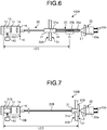
- FIG. 6 is a diagram illustrating a schematic configuration of an optical power transmission apparatus according to a second embodiment.
- An optical power transmission apparatus 100A has a configuration corresponding to the configuration of the optical power transmission apparatus 100 illustrated in FIG. 1 , with the light receiving unit 30 replaced with a light receiving unit 30A.
- the light receiving unit 30A has a configuration corresponding to the light receiving unit 30 of the optical power transmission apparatus 100, with the reflecting mirror 32 replaced with a connector 34 and a fiber Bragg grating (FBG) 35.
- FBG fiber Bragg grating
- the connector 34 is provided at one end of the FBG 35.
- the connector 34 is formed of a known ferrule or optical connector and is connected to the connector connecting unit 31a of the housing 31, so as to be opposed to the connector 21.
- the FBG 35 and the optical fiber 20 are thereby optically connected to each other.
- the connector 34 may be detachably connected to the connector connecting unit 31a or may be bonded to the connector connecting unit 31a.
- the one end of the FBG 35 is polished such that a return loss becomes equal to or greater than 30 dB, the one end being where the connector 34 is provided.
- the FBG 35 is an SMF having a core 35a and a cladding 35b, and a grating G with a periodic refractive index profile is formed in the core 35a.
- the grating G is configured to Bragg-reflect a specific wavelength, and in this embodiment, is configured to transmit a large proportion of light and have a reflectivity of 5%, at the wavelength of 980 nm.
- This FBG 35 functions as a second light reflecting means.
- the other end of the FBG 35 is opposed to the light receiving surface of the light receiving element 33a of the light receiving module 33, and the FBG 35 and the light receiving element 33a are optically connected to each other.
- the optical power transmission apparatus 100A by being optically connected in the order of the reflecting mirror 12 of the light emitting unit 10, the optical fiber 20, and the FBG 35; the reflecting mirror 12, the optical fiber 20, and the FBG 35 form a laser resonator LC2 at the wavelength of 980 nm.
- the laser resonator LC2 is a first laser resonator.
- the semiconductor optical amplifier 11 is arranged in the laser resonator LC2.
- the optical power transmission apparatus 100A operates similarly to the optical power transmission apparatus 100. That is, firstly, the driving device 40 supplies the driving current DC1 to the semiconductor optical amplifier 11. In the state where the semiconductor optical amplifier 11 is generating optical gain, laser oscillation is caused by the laser resonator LC2, and laser light L1 generated by the laser oscillation is output in the light receiving unit 30A from the FBG35 of the laser resonator LC2. As a result, high optical power due to the laser oscillation is transmitted as laser light L1, via the optical fiber 20, from the light emitting unit 10 to the light receiving unit 30. In the light receiving module 33, the light receiving element 33a receives and photoelectrically converts the laser light L1, and the converted electric current is output from the output terminal 33b. When the connector 21 or the connector 34 is detached from the connector connecting unit 31a, the laser resonator LC2 is not formed and laser oscillation does not occur.
- the optical power transmission apparatus 100A enables, with a noncomplex configuration, laser light to be prevented from leaking outside, a high level of safety to be maintained, and safe power supply or power transmission to a remote place or a non-line-of-sight place to be accomplished.
- FIG. 7 is a diagram illustrating a schematic configuration of an optical power transmission apparatus according to a third embodiment.
- An optical power transmission apparatus 100B has a configuration corresponding to the configuration of the optical power transmission apparatus 100 illustrated in FIG. 1 , with the light emitting unit 10 replaced with a light emitting unit 10B, the optical fiber 20 replaced with an optical fiber 20B, and the light receiving unit 30 replaced with a light receiving unit 30B.
- the light emitting unit 10B has a configuration corresponding to the configuration of the light emitting unit 10, with the semiconductor optical amplifier 11 replaced with a semiconductor optical amplifier 11B.
- the semiconductor optical amplifier 11B is made of a material similar to that of the semiconductor optical amplifier 11 and has a structure similar to that of the semiconductor optical amplifier 11, but the width of its active region is set to a width enabling multi-mode waveguiding, for example, 100 ⁇ m.
- the optical fiber 20B is a multi-mode optical fiber (MMF) and has a core diameter of, for example, 100 ⁇ m.
- MMF multi-mode optical fiber
- the light receiving unit 30B has a configuration corresponding to the configuration of the light receiving unit 30 of the optical power transmission apparatus 100, with the reflecting mirror 32 replaced with a volume Bragg grating (VBG) 32B.
- VBG volume Bragg grating
- the VBG 32B is a large-area diffraction grating, and is configured to transmit a large proportion of light and have a reflectivity of 5%, at the wavelength of 980 nm. This VBG 32B functions as a second light reflecting means.
- the VBG 32B is provided on an inner wall of the housing 31, for example, is opposed to the light receiving surface of the light receiving element 33a with a predetermined distance from the light receiving surface, and the VBG 32B and the light receiving element 33a are optically connected to each other.
- the optical power transmission apparatus 100B by being optically connected in the order of the reflecting mirror 12 of the light emitting unit 10B, the optical fiber 20B, and the VBG 32B; the reflecting mirror 12, the optical fiber 20B, and the VBG 32B form a laser resonator LC3 at the wavelength of 980 nm.
- the laser resonator LC3 is a first laser resonator.
- the semiconductor optical amplifier 11B is arranged in the laser resonator LC3.
- the optical power transmission apparatus 100B operates similarly to the optical power transmission apparatus 100. That is, in the state where the semiconductor optical amplifier 11B is being supplied with the driving current DC1 from the driving device 40 and generating optical gain, laser oscillation is caused by the laser resonator LC3, and laser light L3 generated by the laser oscillation is output from the VBG 32B. As a result, high optical power due to the laser oscillation is transmitted as the laser light L3, via the optical fiber 20B, from the light emitting unit 10B to the light receiving unit 30B.
- the width of the active region in the semiconductor optical amplifier 11B is set to a width enabling multi-mode waveguiding and the optical fiber 20B is an MMF, very high optical power of, for example, more than 1 W, is transmitted as the laser light L3.
- the light receiving element 33a receives and photoelectrically converts the laser light L1, and the converted electric current is output from the output terminal 33b.
- the laser resonator LC3 is not formed and laser oscillation does not occur.
- the VBG 32B is separate from the light receiving surface of the light receiving element 33a by a predetermined distance, the beam diameter of the laser light L3 at the light receiving surface is able to be made sufficiently larger than the core diameter of the optical fiber 20B.
- the optical power density at the light receiving surface is able to be reduced and damage to the light receiving surface of the light receiving element 33a is able to be avoided.
- the distance between the VBG 32B and the light receiving surface of the light receiving element 33a is preferably set as appropriate, based on: the resistance of the light receiving element 33a to the optical power density; and the power of the laser light L3.
- the optical fiber 20B is an MMF
- formation of a grating in the core is often difficult generally, and thus use of the VBG 32B is effective.
- the optical power transmission apparatus 100B enables, with a noncomplex configuration, laser light to be prevented from leaking outside, a high level of safety to be maintained, and safe power supply or power transmission to a remote place or to a non-line-of-sight place to be accomplished.
- the photoelectric conversion element includes a semiconductor material having Si as a main constituent.
- the material forming the photoelectric conversion element is not limited to this semiconductor material, and may be selected, as appropriate, according to a wavelength received or the like.
- the photoelectric conversion element may include a semiconductor material lattice matched with gallium arsenide (GaAs). Being lattice-matched herein includes both being unstrained lattice matched and being strained lattice matched. Examples of the semiconductor material lattice matched with GaAs include GaAs and AlGaAs. A configuration having a GaAs layer or an AlGaAs layer formed as an absorption layer on a GaAs substrate may be adopted as a configuration of the photoelectric conversion element.
- the photoelectric conversion element including the semiconductor material lattice matched with GaAs enables the photoelectric conversion efficiency for light of a wavelength near 1000 nm, such as 980 nm, to be increased.
- the photoelectric conversion element may include a semiconductor material lattice matched with indium phosphide (InP).
- the semiconductor material lattice matched with InP include GaInAsP and AlGaInAs.
- a configuration having GaInAsP layers or AlGaInAs layers formed as an absorption layer on an InP substrate may be adopted as a configuration of the photoelectric conversion element.
- the photoelectric conversion element including the semiconductor material lattice matched with InP enables the photoelectric conversion efficiency for light of a wavelength range near 1550 nm, which is one of communication wavelength ranges, to be increased.
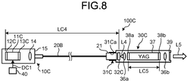
- FIG. 8 is a diagram illustrating a schematic configuration of the optical power transmission apparatus according to the fourth embodiment.
- An optical power transmission apparatus 100C has a configuration corresponding to the configuration of the optical power transmission apparatus 100B illustrated in FIG. 7 , with the light emitting unit 10B replaced with a light emitting unit 10C and the light receiving unit 30B replaced with a light receiving unit 30C.
- the light emitting unit 10C has a configuration corresponding to the configuration of the light emitting unit 10B, with the semiconductor optical amplifier 11B replaced with a semiconductor optical amplifier 11C, the reflecting mirror 12 replaced with a reflecting mirror 12C, and the low-reflecting coating 13 replaced with a low-reflecting coating 13C.
- the semiconductor optical amplifier 11C is made of a material similar to that of the semiconductor optical amplifier 11B and has a structure similar to that of the semiconductor optical amplifier 11B, but the composition of the material and the structure are adjusted such that the semiconductor optical amplifier 11C has a gain wavelength band including 808 nm.
- the reflecting mirror 12C is, for example, a dielectric multilayer and is configured to have a high reflectivity of 95% at 808 nm included in the gain wavelength band of the semiconductor optical amplifier 11.
- the low-reflecting coating 13C is, for example, a dielectric multilayer coating and is configured to have a very low reflectivity of 0.1% at the wavelength of 808 nm.
- the light receiving unit 30C includes a housing 31C, a VBG 32C, lenses 36a and 36b, a microchip 37, reflecting coatings 38a and 38b, and an output window 39.
- the microchip 37 is a second optical gain generating means.
- the housing 31C is a cylindrical housing that houses the VBG 32C, the lenses 36a and 36b, the microchip 37, the reflecting coatings 38a and 38b, and the output window 39, and is made of, for example, a metallic material.
- a connector connecting unit 31Ca connectable to the connector 21 is provided at one end of the housing 31C.
- the VBG 32C is configured to transmit a large proportion of light and have a reflectivity of 5%, at the wavelength of 808 nm.
- the VBG 32C is opposed to one end of the optical fiber 20B, the one end being where the connector 21 is provided.
- the reflecting mirror 12C, the optical fiber 20B, and the VBG 32C form a laser resonator LC4 at the wavelength of 808 nm.
- the laser resonator LC4 is a first laser resonator.
- the semiconductor optical amplifier 11C is arranged in the laser resonator LC4. In a state where the semiconductor optical amplifier 11C is being supplied with the driving current DC1 from the driving device 40 and generating optical gain, laser oscillation is caused by the laser resonator LC4, and laser light L4 generated by the laser oscillation is output from the VBG 32C. As a result, high optical power due to the laser oscillation is transmitted as the laser light L4, via the optical fiber 20B, from the light emitting unit 10C to the light receiving unit 30C.
- the lens 36a is arranged to be opposed to the VBG 32C.
- the lens 36a functions an optical system that causes the laser light L4 to enter the microchip 37.
- the microchip 37 is formed of an optical material including yttrium aluminum garnet (YAG), and in this embodiment, is made of YAG.
- YAG yttrium aluminum garnet
- the reflecting coatings 38a and 38b are respectively provided on opposite facets of the microchip 37, and are, for example, dielectric multilayer coatings.
- the reflecting coating 38a transmits most of the laser light L4 of the wavelength 808 nm, and reflects light of a wavelength of 1064 nm at a high reflectivity (of, for example, 95% or more).
- the reflecting coating 38b is configured to transmit a large proportion of light and have a reflectivity of 50%, at the wavelength of 1064 nm.
- the reflecting coatings 38a and 38b form a laser resonator LC5 that functions at the wavelength of 1064 nm.
- the laser resonator LC5 is a second laser resonator.
- the microchip 37 is arranged in the laser resonator LC5.
- the microchip 37 emits light of the wavelength of 1064 nm and generates optical gain, by receiving the laser light L4 transmitted through the reflecting coating 38a, the laser light L4 serving as excitation light.
- Laser oscillation is then caused by the laser resonator LC5, and laser light L5 of the wavelength of 1064 nm generated by the laser oscillation is output from the reflecting coating 38b of the laser resonator LC5.
- the laser light L5 is second laser light. That is, the reflecting coatings 38a and 38b and the microchip 37 function as a YAG laser unit.
- the lens 36b is arranged to be opposed to the reflecting coating 38b, and functions as a condensing optical system that condenses the laser light L5.
- the output window 39 is an optical window arranged, at the other end of the housing 31C, to be opposed to the lens 36b, and transmits the laser light L5 to output the laser light L5 outside.
- the laser resonator LC4 forms an excitation laser light generating unit for the YAG laser unit.
- the optical power transmission apparatus 100C enables, with a noncomplex configuration, laser light L4 to be prevented from leaking outside, a high level of safety to be maintained, and safe power supply or power transmission to a remote place or to a non-line-of-sight place to be accomplished.
- This optical power transmission apparatus 100C may be suitably used as, for example, an ignition device in an internal combustion engine. Because YAG lasers are able to generate pulsed laser light having very high peak power by pulse excitation, they achieve higher combustion efficiency in internal combustion engines. Examples of a method of providing laser light L4 and laser light L5 as pulsed laser light in the optical power transmission apparatus 100C include a method of providing, as pulsed current, the driving current DC1 supplied from the driving device 40 to the semiconductor optical amplifier 11C. When this optical power transmission apparatus 100C is used as an ignition device, and, for example, the connector 21 is loosened or the light receiving unit 30C is replaced, the replacement corresponding to replacement of the ignition plug, output of the laser light L4 and laser light L5 is automatically stopped and safety is thus maintained.
- This optical power transmission apparatus 100C has an advantage because the light emitting unit 10C is installed at an installable place and optical power is able to be transmitted from that installable place through the optical fiber 20B to the light receiving unit 30C installed in an internal combustion engine.
- the microchip 37 which is the second optical gain generating means, is made of YAG, but a material forming the second optical gain generating means is not limited to YAG, may be yttrium vanadate (YVO), and may be selected as appropriate according to, for example, a desired laser oscillation wavelength.
- YVO yttrium vanadate
- the second optical gain generating means may include a semiconductor material lattice matched with GaAs.
- the semiconductor material lattice matched with GaAs include GaAs, AlGaAs, InGaAs, and AlInGaP.
- a configuration having a GaAs layer, an AlGaAs layer, an InGaAs layer, or an AlInGaP layer formed as a light emitting layer on a GaAs substrate may be adopted as a configuration of the second optical gain generating means.
- the second optical gain generating means including the semiconductor material lattice matched with GaAs is suitable for laser oscillation of a wavelength near 1000 nm, such as 980 nm.
- the second optical gain generating means may include a semiconductor material lattice matched with InP.
- the semiconductor material lattice matched with InP include GaInAsP and AlGaInAs.
- a configuration having GaInAsP layers or AlGaInAs layers formed as a light emitting layer on an InP substrate may be adopted as a configuration of the second optical gain generating means.
- a photoelectric conversion element including the second optical gain generating means lattice matched with InP is suitable for laser oscillation at a wavelength range near 1550 nm, which is one of communication wavelength ranges.
- FIG. 9 is a diagram illustrating a schematic configuration of the optical power transmission device according to the fifth embodiment.
- An optical power transmission apparatus 100D has a configuration corresponding to the configuration of the optical power transmission apparatus 100 illustrated in FIG. 1 , with the light emitting unit 10 replaced with a light emitting unit 10D, the light receiving unit 30 replaced with a light receiving unit 30D, and a headlight unit 50 added.
- the optical power transmission apparatus 100D is applied to a laser headlight of an automobile.
- Laser head lights have an advantage that the spot size of light is able to be made small, high-intensity lighting is enabled, and bright illumination over a long distance of some hundreds of meters is enabled.
- the light emitting unit 10D has a configuration corresponding to the configuration of the light emitting unit 10, with the semiconductor optical amplifier 11 replaced with a semiconductor optical amplifier 11D, the reflecting mirror 12 replaced with a reflecting mirror 12D, and the low-reflecting coating 13 replaced with a low-reflecting coating 13D.
- a composition of the material and the structure of the semiconductor optical amplifier 11D are adjusted such that its gain wavelength band includes 400 nm, which is a blue wavelength (360 nm to 480 nm).
- the reflecting mirror 12D is, for example, a dielectric multilayer coating, and is configured to have a high reflectivity of 95% at the wavelength of 400 nm.
- the low-reflecting coating 13D is, for example, a dielectric multilayer coating and is configured to have a very low reflectivity of 0.1% at the wavelength of 440 nm.
- the light emitting unit 10 is attached to a member having high heat dissipation performance in an automobile, a frame F of the body of a car in this embodiment.
- the light receiving unit 30D includes a housing 31D, and a reflecting mirror 32D housed in the housing 31D.
- the reflecting mirror 32D is a second light reflecting means.
- the optical fiber 20 is inserted in the housing 31D and is fixed to the housing 31D such that one end of the optical fiber 20 is near and opposed to the reflecting mirror 32D.
- the optical fiber 20 and the reflecting mirror 32D are thereby optically connected to each other.
- the reflecting mirror 32D is, for example, an optical plate (for example, a glass plate) having a dielectric multilayer coating formed thereon, and is configured to transmit a large proportion of light and have a reflectivity of 5%, at the wavelength of 400 nm.
- the laser resonator LC6 is a first laser resonator.
- the semiconductor optical amplifier 11D is arranged in the laser resonator LC6. In a state where the semiconductor optical amplifier 11D is being supplied with the driving current DC1 from the driving device 40 and generating optical gain, laser oscillation is caused by the laser resonator LC6, and laser light L6 generated by the laser oscillation is output from the reflecting mirror 32D. As a result, high optical power due to the laser oscillation is transmitted as the laser light L6 from the light emitting unit 10D to the light receiving unit 30D, via the optical fiber 20.
- the laser light L6 is first laser light.
- the headlight unit 50 includes a housing 51, a reflecting mirror 52, a light emitting unit 53, a reflecting mirror 54, and a projection lens 55.
- the housing 51 is made of, for example, resin, and houses the reflecting mirror 52, the light emitting unit 53, and the reflecting mirror 54, and the projection lens 55 is attached to the housing 51 such that the projection lens 55 is exposed outside. Furthermore, the light receiving unit 30D is attached to the housing 51.
- the reflecting mirror 52 reflects the laser light L6 output from the light receiving unit 30D to the light emitting unit 53.
- the light emitting unit 53 is made of a resin including a known fluorescent material that absorbs blue light and emits yellow light in the complementary color of blue light. Therefore, the light emitting unit 53 absorbs part of the laser light L6 and emits yellow light having a wavelength different from that of the laser light L6. The light emitting unit 53 thereby outputs white light L7.
- the reflecting mirror 54 is a concave mirror, condenses the white light L7, and reflects the condensed white light L7 to the projection lens 55.
- the projection lens 55 condenses the white light L7 and outputs the condensed white light L7 outside.
- the configuration of the light emitting unit 53 is just an example, and is not limited to this example.
- the optical power transmission apparatus 100D enables, with a noncomplex configuration, the laser light L6 to be prevented from leaking outside and a high level of safety to be maintained. Furthermore, a space enabling installation of the light emitting unit 10D near the headlight unit 50 may be unable to be obtained in an automobile.
- This optical power transmission apparatus 100D has an advantage because the light emitting unit 10D is installed at an installable place and optical power is able to be transmitted from the installable place to the light receiving unit 30D installed at the headlight unit 50 via the optical fiber 20.
- the optical power transmission apparatus 100D has a desirable configuration in terms of countermeasures against heat.
- FIG. 10 is a diagram illustrating a schematic configuration of a headlight unit with a built-in blue laser light source.
- This headlight unit 350 has a blue laser light source 310 housed in a housing 351.
- the blue laser light source 310 is supplied with electric current from a terminal 311 and outputs blue laser light L31.
- a reflecting mirror 352 reflects the laser light L31 output from the blue laser light source 310 to a light emitting unit 353.
- the light emitting unit 353 absorbs part of the laser light L31 and emits yellow light in the complementary color thereof, thereby outputting white light L32.
- a reflecting mirror 354 is a concave mirror, condenses the white light L32 and reflects the condensed white light L32 to a projection lens 355.
- the projection lens 355 condenses the white light L32 and outputs the condensed white light L32 outside.
- This headlight unit 350 has a structure in which the high intensity blue laser light source 310 is incorporated in the highly sealable housing 351, and thus has a problem in the heat dissipation performance for heat generated by the blue laser light source 310.
- the light emitting unit 10D is installed in close contact with a member having high heat dissipation performance, such as the frame F, and optical power is transmitted as the laser light L6 via the optical fiber 20 to near the light emitting unit 53 of the headlight unit 50. Furthermore, if the optical fiber 20 is detached, laser oscillation is stopped. As a result, a laser headlight system that has excellent heat dissipation performance and is safe is able to be provided.
- the first optical gain generating means is a semiconductor optical amplifier, but the first optical gain generating means may be another optical gain generating means used in a solid-state laser, such as a YAG rod, for example.
- the energy supplying means is, for example, a laser light source, and energy that causes the YAG rod to generate gain is supplied via light.
- the present invention is suitable for application to optical power transmission using optical fiber.
Landscapes
- Physics & Mathematics (AREA)
- Electromagnetism (AREA)
- Engineering & Computer Science (AREA)
- Optics & Photonics (AREA)
- Plasma & Fusion (AREA)
- Condensed Matter Physics & Semiconductors (AREA)
- General Physics & Mathematics (AREA)
- Microelectronics & Electronic Packaging (AREA)
- Signal Processing (AREA)
- Chemical & Material Sciences (AREA)
- Combustion & Propulsion (AREA)
- Mechanical Engineering (AREA)
- General Engineering & Computer Science (AREA)
- Computer Networks & Wireless Communication (AREA)
- Semiconductor Lasers (AREA)
- Optical Couplings Of Light Guides (AREA)
- Lasers (AREA)
Abstract
Description
- The present invention relates to optical power transmission apparatuses that transmit optical power over optical fiber.
- Power-over-fiber is an application example of optical power transmission using optical fiber. Power-over-fiber is a technology in which laser light output from a high-power laser light source is transmitted to a remote place using optical fiber, photoelectric conversion is performed at a light receiving unit and energy of the laser light is thereby converted to electric power, and an electric device is driven by the electric power. Power-over-fiber has, as compared to conventional power supply using copper wire, many advantages including: not being electromagnetically induced and thus being resistant to noise and not generating noise; high resistance to thunderstrokes; not having electrical contacts and thus being usable even under highly humid environments; and being explosion proof. Such optical power transmission has been studied for ignition devices in internal combustion engines of automobiles, for example (Non-Patent Literature 1) .
- However, there is a risk that any laser light that leaks outside and radiates from the power supply path may harm human bodies and surrounding objects. Patent Literature 1 discloses a configuration, in which voltage output from a photoelectric conversion means is detected and an optical power stopping means that immediately stops the laser power source if an abnormality is detected operates to avoid such a risk.
- Furthermore, Patent Literature 2 similarly discloses a technique, in which signal light including error information is transmitted from a light receiving end to a light emitting end if an appropriate signal is unable to be received at the receiving end, and driving of a laser light source for power supply is stopped according to an instruction from a control unit.
- Optical wireless power supply technologies not using optical fiber include a technology, in which a laser resonator is formed between a light emitting unit and a light receiving unit, the light emitting unit including a combination of a retroreflector and a gain means, the light receiving unit including a combination of a retroreflector and a light receiving means, and laser oscillation is thereby immediately stopped when a shielding object, such as a human body, is inserted into the optical path of the resonator, as disclosed in Patent Literature 3.
-
- Patent Literature 1: Japanese Laid-open Patent Publication No.
2001-037105 - Patent Literature 2: Japanese Laid-open Patent Publication No.
2008-193327 - Patent Literature 3:
US Patent No. 9705606 - Non-Patent Literature 1: TAIRA Takunori, et al., "Promise of Giant Pulse Micro-Laser for Engine Ignition", J. Plasma Fusion Res. Vol. 89, No. 4, pp. 238, 2013
- However, for power-over-fiber, the method of detecting an abnormality at a light receiving end and feeding back the abnormality to a light emitting end, as disclosed in Patent Literature 1 and Patent Literature 2, additionally requires an abnormality detecting means and a circuit for stopping the operation of the laser light source and the system configuration may thus become complex. Furthermore, this method involves processing including abnormality detection and signal processing, and thus has a problem that laser oscillation may occur due to a malfunction in the mechanism implementing the processing, such as the abnormality detection or the signal processing, even if laser oscillation is supposed to be stopped.
- In contrast, the optical wireless power supply system described in Patent Literature 3 maintains higher safety. However, when the distance between the light emitting unit and the light receiving unit is increased, power transmission loss is dramatically increased and laser oscillation will no longer occur. A practical power transmission distance therefor would thus be a few meters. Furthermore, if there is an obstacle between the light emitting unit and the light receiving unit, optical power is unable to be transmitted, and the environment for their installation is thus limited to a small line-of-sight space.
- The present invention has been made in view of the above, and aims to provide an optical power transmission apparatus that maintains a high level of safety with a noncomplex configuration and enables optical power transmission over a long distance or to a non-line-of-sight place.
- To resolve the above and attain the object, an optical power transmission apparatus according to an embodiment of the present invention, includes: a light emitting unit including a first optical gain generating means and a first light reflecting means; an optical fiber; a second light reflecting means; and a light receiving means. Further, the second light reflecting means is arranged nearer to the light receiving means than the optical fiber is, a first laser resonator is formed, between the first light reflecting means and the second light reflecting means, by optical connection between the first optical gain generating means and the optical fiber, and first laser light generated by the first laser resonator is configured to be incident on the light receiving means.
- In the optical power transmission apparatus according to an embodiment of the present invention, the second light reflecting means and the light receiving means are fixed to each other to form a light receiving unit.
- In the optical power transmission apparatus according to an embodiment of the present invention, comprising an energy supplying means that supplies energy to the first optical gain generating means.
In the optical power transmission apparatus according to an embodiment of the present invention, - In the optical power transmission apparatus according to an embodiment of the present invention, the optical fiber is configured to be able to be optically decoupled from the second light reflecting means.
- In the optical power transmission apparatus according to an embodiment of the present invention, the optical fiber has a first fixing unit near the light receiving unit, the light receiving unit has a second fixing unit, and the first fixing unit is detachably connected to the second fixing unit that is installed at a predetermined position enabling optical connection between the optical fiber and the second light reflecting means.
- In the optical power transmission apparatus according to an embodiment of the present invention, the energy supplying means is configured to supply, to the first optical gain generating means, energy of values: in a range where the laser oscillation occurs in a state where the first light reflecting means, the optical fiber, and the second light reflecting means have been optically connected to one another; and in a range where the laser oscillation does not occur in a case where the optical connection has been cancelled.
- In the optical power transmission apparatus according to an embodiment of the present invention, the first optical gain generating means is a semiconductor optical amplifier.
- In the optical power transmission apparatus according to an embodiment of the present invention, the light receiving means is a photoelectric conversion element that receives the first laser light output from the first laser resonator and converts the received first laser light into electric current.
- In the optical power transmission apparatus according to an embodiment of the present invention, the photoelectric conversion element includes a semiconductor material having silicon (Si) as a main constituent.
- In the optical power transmission apparatus according to an embodiment of the present invention, the photoelectric conversion element includes a semiconductor material lattice matched with gallium arsenide (GaAs).
- In the optical power transmission apparatus according to an embodiment of the present invention, the photoelectric conversion element includes a semiconductor material lattice matched with indium phosphide (InP).
- In the optical power transmission apparatus according to an embodiment of the present invention, the light receiving unit includes a second laser resonator, and a second optical gain generating means that is arranged in the second laser resonator and generates optical gain by being supplied with energy, the second optical gain generating means receives the first laser light and generates optical gain, and laser oscillation is caused by the second laser resonator, and second laser light generated by the laser oscillation is configured to be output from the second laser resonator.
- In the optical power transmission apparatus according to an embodiment of the present invention, the second optical gain generating means is formed of an optical material including yttrium aluminum garnet (YAG).
- In the optical power transmission apparatus according to an embodiment of the present invention, the second optical gain generating means includes a semiconductor material lattice matched with gallium arsenide (GaAs).
- In the optical power transmission apparatus according to an embodiment of the present invention, the second optical gain generating means includes a semiconductor material lattice matched with indium phosphide (InP).
- In the optical power transmission apparatus according to an embodiment of the present invention, the light receiving means is a light emitting means that absorbs the first laser light output from the first laser resonator and emits light having a wavelength different from a wavelength of the first laser light.
- The present invention has an effect of maintaining a high level of safety with a noncomplex configuration and enabling optical power transmission over a long distance or to a non-line-of-sight place.
-
-
FIG. 1 is a diagram illustrating a schematic configuration of an optical power transmission apparatus according to a first embodiment. -
FIG. 2 is a diagram illustrating the optical power transmission apparatus inFIG. 1 in a state where laser oscillation is stopped. -
FIG. 3 is a diagram illustrating a schematic configuration of an optical power transmission apparatus as Comparative Example. -
FIG. 4 is a diagram illustrating an example of relations between driving current and output current. -
FIG. 5 is a diagram illustrating another example of the relations between driving current and output current. -
FIG. 6 is a diagram illustrating a schematic configuration of an optical power transmission apparatus according to a second embodiment. -
FIG. 7 is a diagram illustrating a schematic configuration of an optical power transmission apparatus according to a third embodiment. -
FIG. 8 is a diagram illustrating a schematic configuration of an optical power transmission apparatus according to a fourth embodiment. -
FIG. 9 is a diagram illustrating a schematic configuration of an optical power transmission apparatus according to a fifth embodiment. -
FIG. 10 is a diagram illustrating a schematic configuration of a headlight unit. - Hereinafter, embodiments of the present invention will be described in detail while reference is made to the appended drawings. The present invention is not limited by the embodiments described below. Furthermore, the same signs will be assigned, as appropriate, to the same or corresponding elements in the drawings, and redundant description thereof will be omitted, as appropriate. In addition, it needs to be noted that the drawings are schematic, and relations among dimensions of the elements therein may be different from the actual relations. A portion having different dimensional relations and ratios among the drawings may be included, too.
-
FIG. 1 is a diagram illustrating a schematic configuration of an optical power transmission apparatus according to a first embodiment. An opticalpower transmission apparatus 100 includes alight emitting unit 10, anoptical fiber 20, alight receiving unit 30, and adriving device 40. The drivingdevice 40 is an energy supplying means. - The
light emitting unit 10 includes: a semiconductoroptical amplifier 11; a reflectingmirror 12; a low-reflectingcoating 13; alens 14; and ahousing 15. The semiconductoroptical amplifier 11 is a first optical gain generating means, and the reflectingmirror 12 is a first light reflecting means. - The driving
device 40 is a known driving device configured to be able to drive the semiconductoroptical amplifier 11. The drivingdevice 40 supplies driving current DC1 serving as energy, to the semiconductoroptical amplifier 11. - The semiconductor
optical amplifier 11 according to this embodiment has a strained quantum well structure formed as an active layer, on a gallium arsenide (GaAs) substrate. The strained quantum well structure includes a constituent material that is GaInAs, which is a semiconductor material. The width of an active region including an active layer in the semiconductoroptical amplifier 11 is configured to be a width enabling single-mode waveguiding, for example, 2 µm. The semiconductoroptical amplifier 11 is a diced chip obtained by cleavage of a wafer into chips each having a length of 1 mm in the optical waveguiding direction. The semiconductoroptical amplifier 11 emits light by being supplied with the driving current DC1 from the drivingdevice 40 and generates optical gain. The semiconductoroptical amplifier 11 is configured by adjustment of the composition or the like of the strained quantum well structure such that the semiconductoroptical amplifier 11 has a gain wavelength band including 980 nm. - The reflecting
mirror 12 is formed on one of cleaved facets of the semiconductoroptical amplifier 11, the cleaved facets both being on an optical waveguiding path of the semiconductoroptical amplifier 11. The reflectingmirror 12 is, for example, a dielectric multilayer coating and is configured to have a high reflectivity of 95% at 980 nm included in the gain wavelength band of the semiconductoroptical amplifier 11. - The low-reflecting
coating 13 is formed on the other one of the cleaved facets such that the low-reflectingcoating 13 is opposed to the reflectingmirror 12 with the semiconductoroptical amplifier 11 interposed between the low-reflectingcoating 13 and the reflectingmirror 12, the cleaved facets both being on the optical waveguiding path. The low-reflectingcoating 13 is, for example, a dielectric multilayer coating and is configured to have a very low reflectivity of 0.1% at the wavelength of 980 nm. - The
lens 14 is arranged on one side of the low-reflectingcoating 13, the one side being opposite to where the semiconductoroptical amplifier 11 is. Thelens 14 optically couples light generated by the semiconductoroptical amplifier 11 and output via the low-reflectingcoating 13, to one end of theoptical fiber 20. - The
housing 15 is a housing that houses the semiconductoroptical amplifier 11, the reflectingmirror 12, the low-reflectingcoating 13, and thelens 14, and is made of, for example, a metallic material. Furthermore, the one end of theoptical fiber 20 is connected to thehousing 15. - The
optical fiber 20 connects thelight emitting unit 10 and thelight receiving unit 30 to each other, and is, according to this embodiment, a single-mode optical fiber (SMF). The one end of theoptical fiber 20 is processed into a lens shape, the one end being connected to thehousing 15, and is, as described above, optically connected, at the facet where the low-reflectingcoating 13 is formed, to the semiconductoroptical amplifier 11, via thelens 14. Aconnector 21 is provided at the other end of theoptical fiber 20 and theconnector 21 is connected to thelight receiving unit 30. Theconnector 21 is formed of a known ferrule or optical connector. The other end of theoptical fiber 20 is polished such that a return loss becomes equal to or greater than 30 dB (that is, a reflectivity becomes equal to or less than 0.1%), the other end being where theconnector 21 is provided. Theconnector 21 corresponds to a first fixing unit that theoptical fiber 20 has near thelight receiving unit 30. - The
light receiving unit 30 includes ahousing 31, a reflectingmirror 32, and alight receiving module 33. The reflectingmirror 32 is a second light reflecting means. - The
housing 31 is a housing that houses the reflectingmirror 32 and thelight receiving module 33, and is made of, for example, a metallic material. Furthermore, thehousing 31 has aconnector connecting unit 31a provided therein. Theconnector 21 is connectable to theconnector connecting unit 31a. Theoptical fiber 20 is connected to thelight receiving unit 30 by connection of theconnector 21 to theconnector connecting unit 31a. Theconnector 21 may be detachably connected to theconnector connecting unit 31a or may be bonded to theconnector connecting unit 31a. - The reflecting
mirror 32 is arranged near theconnector connecting unit 31a. Specifically, the reflectingmirror 32 is arranged such that a reflecting surface of the reflectingmirror 32 is opposed to the other end of theoptical fiber 20 at a short distance, for example, at a short distance where the reflecting surface substantially touches the other end, in a state where theconnector 21 has been connected to theconnector connecting unit 31a. Theoptical fiber 20 and the reflectingmirror 32 are thereby optically connected to each other. Therefore, theconnector connecting unit 31a corresponds to a second fixing unit placed at a predetermined position (at thelight receiving unit 30 according to this embodiment), the predetermined position enabling optical connection between theoptical fiber 20 and the reflectingmirror 32. Theconnector 21 serving as the first fixing unit is connected to theconnector connecting unit 31a serving as the second fixing unit. The reflectingmirror 32 is, for example, an optical plate (such as a glass plate) having a dielectric multilayer coating formed thereon, for example, and is configured to transmit a large proportion of light and have a reflectivity of 5%, at the wavelength of 980 nm. - The
light receiving module 33 includes alight receiving element 33a and anoutput terminal 33b. Thelight receiving element 33a is a photoelectric conversion element that converts light received, into electric current of quantity corresponding to the received power of the light, and is, for example, a photodiode. A low-reflecting coating is preferably formed on a light receiving surface of thelight receiving element 33a. Theoutput terminal 33b is electrically connected to thelight receiving element 33a and is a terminal for outputting electric current. In this embodiment, thelight receiving element 33a includes a semiconductor material having silicon (Si) as a main constituent, and is made of, for example, Si. The semiconductor material having Si as the main constituent is a semiconductor material, in which 50% or more of its composition is Si, for example, in which 99% or more of its composition is Si, and 1% or less of its composition corresponds to other impurities. Light receiving sensitivity of Si to light of a wavelength near 1000 nm, such as the wavelength of 980 nm, is high and Si is inexpensive. - By being optically connected in the order of the reflecting
mirror 12, theoptical fiber 20, and the reflectingmirror 32; the reflectingmirror 12, theoptical fiber 20, and the reflectingmirror 32 form a laser resonator LC1 at the wavelength of 980 nm. The laser resonator LC1 is a first laser resonator. The semiconductoroptical amplifier 11 is arranged in the laser resonator LC1. - Operation of the optical
power transmission apparatus 100 will now be described. Firstly, the drivingdevice 40 supplies the driving current DC1, to the semiconductoroptical amplifier 11. The semiconductoroptical amplifier 11 then emits light of a wavelength in a gain bandwidth of the semiconductoroptical amplifier 11 and generates optical gain. In the state where the semiconductoroptical amplifier 11 is generating the optical gain, laser oscillation is then caused by the laser resonator LC1, and laser light L1 generated by the laser oscillation is output from the laser resonator LC1, in thelight receiving unit 30. The laser light L1 is first laser light. Specifically, in thelight receiving unit 30, the laser light L1 is output from the reflectingmirror 32 forming one end of the laser resonator LC1. That is, the opticalpower transmission apparatus 100 is configured to output the laser light L1 generated by the laser resonator LC1, from the laser resonator LC1, in thelight receiving unit 30. As a result, high optical power due to the laser oscillation is transmitted as the laser light L1, via theoptical fiber 20, from thelight emitting unit 10 to thelight receiving unit 30. In thelight receiving module 33, thelight receiving element 33a receives and photoelectrically converts the laser light L1, and the converted electric current is output from theoutput terminal 33b. - As illustrated in
FIG. 2 , when theconnector 21 is detached from theconnector connecting unit 31a, the optical connection between the reflectingmirror 12, theoptical fiber 20, and the reflectingmirror 32 is cancelled. In this case, the laser resonator LC1 is not formed. As a result, laser oscillation does not occur, and light L2 low in power without laser oscillation is output from theconnector 21 of theoptical fiber 20. - As described above, in the optical
power transmission apparatus 100, in the state where laser oscillation by the laser resonator LC1 is occurring, high optical power is transmitted, and in the state where the laser resonator LC1 has not been formed, laser oscillation does not occur and the light L2 low in power is output. Therefore, in this opticalpower transmission apparatus 100, if an abnormality occurs, for example, in a case where theconnector 21 of theoptical fiber 20 is detached, theconnector 21 connecting thelight emitting unit 10 and thelight receiving unit 30 to each other, laser oscillation is automatically stopped. Accordingly, with a noncomplex configuration not having an abnormality detecting means in the light receiving unit nor a stopping means in the light emitting unit, laser light is prevented from leaking outside and a high level of safety is able to be maintained. Furthermore, the use of theoptical fiber 20 enables safe power supply or power transmission to a remote place or a non-line-of-sight place, to which power supply or power transmission is not made possible by optical wireless power supply. - As Example, an optical power transmission apparatus having the same configuration as the optical
power transmission apparatus 100 according to the first embodiment was manufactured, and driving current was supplied to its semiconductor optical amplifier for measurement of characteristics thereof. Furthermore, as Comparative Example, an optical power transmission apparatus having the same configuration as an opticalpower transmission apparatus 200 illustrated inFIG. 3 was manufactured, and driving current was supplied to its semiconductor optical amplifier for measurement of characteristics thereof. The opticalpower transmission apparatus 200 has alight receiving unit 230 having a configuration corresponding to thelight receiving unit 30 of the opticalpower transmission apparatus 100, with the reflectingmirror 32 eliminated from thelight receiving unit 30. -
FIG. 4 is a diagram illustrating an example of relations between driving current and output current of the light receiving units. InFIG. 4 , the horizontal axis corresponds to driving current supplied to the semiconductor optical amplifiers and the vertical axis corresponds to output current from the light receiving modules in the light receiving units. As indicated by a line L11, in Example, laser oscillation occurred and output current was generated, when the driving current exceeded a current I1 (about 50 mA). When the driving current was about 500 mA, output current of about 200 mA, that is, electric power of about 150 mW assuming the voltage to be 0.75 V, was acquired in the light receiving unit. - On the contrary, as indicated by a line L12, in Comparative Example, it was confirmed that laser oscillation did not occur and output current was not generated when the driving current was just about 500 mA. This is considered to indicate that at a driving current of about 500 mA, in a state where a laser resonator has not been formed, like in a case where the connector of the optical fiber has been detached, laser oscillation is automatically stopped and leakage to the outside does not occur.
- In Comparative Example also, laser oscillation occurs when the driving current exceeds a current I2 (about 650 mA). Therefore, to maintain safety more infallibly, the driving device preferably controls the driving current by being configured to supply electric current of values: in a range where laser oscillation occurs in a case where predetermined optical connection has been achieved and a laser resonator has been formed; and in a range where laser oscillation does not occur in a state where the predetermined optical connection has been cancelled and the laser resonator has not been formed.
- Next,
FIG. 5 is a diagram illustrating another example of the relations between driving current and output current. Lines L21 and L22 respectively indicate the relations for optical power transmission apparatuses corresponding to the above described optical power transmission apparatuses of Example and Comparative Example, with 1-mm chips of their semiconductor optical amplifiers replaced with 3-mm chips, the 1-mm chips each having a length of 1 mm in the optical waveguiding direction, the 3-mm chips each having a length of 3 mm in the optical waveguiding direction. As illustrated inFIG. 5 , when the lengths of the semiconductor optical amplifiers are 3 mm, the relations between the driving current and the output current are not much different from each other. That is, in a state where the driving current is equal to or less than 100 mA, the output current starts to increase, and at a driving current of 500 mA, an output current of about 200 mA has been acquired. - This is considered to be caused because when the semiconductor optical amplifiers are long, the gain is also high, and thus even if there is no reflection by the reflecting mirrors in the light receiving units, laser oscillation is caused by influence of the reflection (for example, of a reflectivity of 0.1%) at the low-reflecting coatings of the semiconductor optical amplifiers, for example. Therefore, the driving current and the gain of the semiconductor optical amplifier need to be set appropriately, for example, for a configuration enabling laser oscillation by the first laser resonator. Furthermore, optical fiber has transmission loss dependent on wavelength, and the value of the transmission loss is, for example, about 3 dB/km at the wavelength of 980 nm. Therefore, if an optical fiber having a length making its transmission loss non-negligible is used, a condition necessary for laser oscillation becomes severer, for example, the reflectivity of the reflecting mirror in the light receiving unit becomes higher. Accordingly, there is an appropriate reflectivity for a length of optical fiber. These various parameters affecting laser oscillation in the first laser resonator are desirably set as appropriate such that laser oscillation is caused by the first laser resonator according to: a transmission distance; electric output required at the light receiving unit; electric power consumption allowed at the light emitting unit; and the like.
- In this embodiment, the reflecting
mirror 32, which is the second light reflecting means, is an optical plate having a dielectric multilayer coating formed thereon, but the second light reflecting means is not limited to such an optical plate, and may be a dielectric multilayer coating formed on the light receiving surface of thelight receiving element 33a. -
FIG. 6 is a diagram illustrating a schematic configuration of an optical power transmission apparatus according to a second embodiment. An opticalpower transmission apparatus 100A has a configuration corresponding to the configuration of the opticalpower transmission apparatus 100 illustrated inFIG. 1 , with thelight receiving unit 30 replaced with alight receiving unit 30A. - The
light receiving unit 30A has a configuration corresponding to thelight receiving unit 30 of the opticalpower transmission apparatus 100, with the reflectingmirror 32 replaced with aconnector 34 and a fiber Bragg grating (FBG) 35. - The
connector 34 is provided at one end of theFBG 35. Theconnector 34 is formed of a known ferrule or optical connector and is connected to theconnector connecting unit 31a of thehousing 31, so as to be opposed to theconnector 21. TheFBG 35 and theoptical fiber 20 are thereby optically connected to each other. Theconnector 34 may be detachably connected to theconnector connecting unit 31a or may be bonded to theconnector connecting unit 31a. The one end of theFBG 35 is polished such that a return loss becomes equal to or greater than 30 dB, the one end being where theconnector 34 is provided. - The
FBG 35 is an SMF having acore 35a and acladding 35b, and a grating G with a periodic refractive index profile is formed in thecore 35a. The grating G is configured to Bragg-reflect a specific wavelength, and in this embodiment, is configured to transmit a large proportion of light and have a reflectivity of 5%, at the wavelength of 980 nm. ThisFBG 35 functions as a second light reflecting means. The other end of theFBG 35 is opposed to the light receiving surface of thelight receiving element 33a of thelight receiving module 33, and theFBG 35 and thelight receiving element 33a are optically connected to each other. - In the optical
power transmission apparatus 100A, by being optically connected in the order of the reflectingmirror 12 of thelight emitting unit 10, theoptical fiber 20, and theFBG 35; the reflectingmirror 12, theoptical fiber 20, and theFBG 35 form a laser resonator LC2 at the wavelength of 980 nm. The laser resonator LC2 is a first laser resonator. The semiconductoroptical amplifier 11 is arranged in the laser resonator LC2. - The optical
power transmission apparatus 100A operates similarly to the opticalpower transmission apparatus 100. That is, firstly, the drivingdevice 40 supplies the driving current DC1 to the semiconductoroptical amplifier 11. In the state where the semiconductoroptical amplifier 11 is generating optical gain, laser oscillation is caused by the laser resonator LC2, and laser light L1 generated by the laser oscillation is output in thelight receiving unit 30A from the FBG35 of the laser resonator LC2. As a result, high optical power due to the laser oscillation is transmitted as laser light L1, via theoptical fiber 20, from thelight emitting unit 10 to thelight receiving unit 30. In thelight receiving module 33, thelight receiving element 33a receives and photoelectrically converts the laser light L1, and the converted electric current is output from theoutput terminal 33b. When theconnector 21 or theconnector 34 is detached from theconnector connecting unit 31a, the laser resonator LC2 is not formed and laser oscillation does not occur. - Therefore, similarly to the optical
power transmission apparatus 100, the opticalpower transmission apparatus 100A enables, with a noncomplex configuration, laser light to be prevented from leaking outside, a high level of safety to be maintained, and safe power supply or power transmission to a remote place or a non-line-of-sight place to be accomplished. -
FIG. 7 is a diagram illustrating a schematic configuration of an optical power transmission apparatus according to a third embodiment. An opticalpower transmission apparatus 100B has a configuration corresponding to the configuration of the opticalpower transmission apparatus 100 illustrated inFIG. 1 , with thelight emitting unit 10 replaced with alight emitting unit 10B, theoptical fiber 20 replaced with anoptical fiber 20B, and thelight receiving unit 30 replaced with alight receiving unit 30B. - The
light emitting unit 10B has a configuration corresponding to the configuration of thelight emitting unit 10, with the semiconductoroptical amplifier 11 replaced with a semiconductoroptical amplifier 11B. The semiconductoroptical amplifier 11B is made of a material similar to that of the semiconductoroptical amplifier 11 and has a structure similar to that of the semiconductoroptical amplifier 11, but the width of its active region is set to a width enabling multi-mode waveguiding, for example, 100 µm. - The
optical fiber 20B is a multi-mode optical fiber (MMF) and has a core diameter of, for example, 100 µm. - The
light receiving unit 30B has a configuration corresponding to the configuration of thelight receiving unit 30 of the opticalpower transmission apparatus 100, with the reflectingmirror 32 replaced with a volume Bragg grating (VBG) 32B. - The
VBG 32B is a large-area diffraction grating, and is configured to transmit a large proportion of light and have a reflectivity of 5%, at the wavelength of 980 nm. ThisVBG 32B functions as a second light reflecting means. TheVBG 32B is provided on an inner wall of thehousing 31, for example, is opposed to the light receiving surface of thelight receiving element 33a with a predetermined distance from the light receiving surface, and theVBG 32B and thelight receiving element 33a are optically connected to each other. - In the optical
power transmission apparatus 100B, by being optically connected in the order of the reflectingmirror 12 of thelight emitting unit 10B, theoptical fiber 20B, and theVBG 32B; the reflectingmirror 12, theoptical fiber 20B, and theVBG 32B form a laser resonator LC3 at the wavelength of 980 nm. The laser resonator LC3 is a first laser resonator. The semiconductoroptical amplifier 11B is arranged in the laser resonator LC3. - The optical
power transmission apparatus 100B operates similarly to the opticalpower transmission apparatus 100. That is, in the state where the semiconductoroptical amplifier 11B is being supplied with the driving current DC1 from the drivingdevice 40 and generating optical gain, laser oscillation is caused by the laser resonator LC3, and laser light L3 generated by the laser oscillation is output from theVBG 32B. As a result, high optical power due to the laser oscillation is transmitted as the laser light L3, via theoptical fiber 20B, from thelight emitting unit 10B to thelight receiving unit 30B. - In particular, in the optical
power transmission apparatus 100B, because the width of the active region in the semiconductoroptical amplifier 11B is set to a width enabling multi-mode waveguiding and theoptical fiber 20B is an MMF, very high optical power of, for example, more than 1 W, is transmitted as the laser light L3. - In a light receiving module 33B, the
light receiving element 33a receives and photoelectrically converts the laser light L1, and the converted electric current is output from theoutput terminal 33b. When theconnector 21 is detached from theconnector connecting unit 31a, the laser resonator LC3 is not formed and laser oscillation does not occur. - Furthermore, in the optical
power transmission apparatus 100B, because theVBG 32B is separate from the light receiving surface of thelight receiving element 33a by a predetermined distance, the beam diameter of the laser light L3 at the light receiving surface is able to be made sufficiently larger than the core diameter of theoptical fiber 20B. As a result, the optical power density at the light receiving surface is able to be reduced and damage to the light receiving surface of thelight receiving element 33a is able to be avoided. The distance between theVBG 32B and the light receiving surface of thelight receiving element 33a is preferably set as appropriate, based on: the resistance of thelight receiving element 33a to the optical power density; and the power of the laser light L3. - Furthermore, when the
optical fiber 20B is an MMF, formation of a grating in the core is often difficult generally, and thus use of theVBG 32B is effective. - Similarly to the optical
power transmission apparatus 100, the opticalpower transmission apparatus 100B enables, with a noncomplex configuration, laser light to be prevented from leaking outside, a high level of safety to be maintained, and safe power supply or power transmission to a remote place or to a non-line-of-sight place to be accomplished. - In the above described embodiments, the photoelectric conversion element includes a semiconductor material having Si as a main constituent. However, the material forming the photoelectric conversion element is not limited to this semiconductor material, and may be selected, as appropriate, according to a wavelength received or the like.
- For example, the photoelectric conversion element may include a semiconductor material lattice matched with gallium arsenide (GaAs). Being lattice-matched herein includes both being unstrained lattice matched and being strained lattice matched. Examples of the semiconductor material lattice matched with GaAs include GaAs and AlGaAs. A configuration having a GaAs layer or an AlGaAs layer formed as an absorption layer on a GaAs substrate may be adopted as a configuration of the photoelectric conversion element. The photoelectric conversion element including the semiconductor material lattice matched with GaAs enables the photoelectric conversion efficiency for light of a wavelength near 1000 nm, such as 980 nm, to be increased.
- Furthermore, the photoelectric conversion element may include a semiconductor material lattice matched with indium phosphide (InP). Examples of the semiconductor material lattice matched with InP include GaInAsP and AlGaInAs. A configuration having GaInAsP layers or AlGaInAs layers formed as an absorption layer on an InP substrate may be adopted as a configuration of the photoelectric conversion element. The photoelectric conversion element including the semiconductor material lattice matched with InP enables the photoelectric conversion efficiency for light of a wavelength range near 1550 nm, which is one of communication wavelength ranges, to be increased.
- An optical power transmission apparatus that uses, as is, light transmitted through an optical fiber, without converting the optical power into electricity, will be described as a fourth embodiment.
FIG. 8 is a diagram illustrating a schematic configuration of the optical power transmission apparatus according to the fourth embodiment. An opticalpower transmission apparatus 100C has a configuration corresponding to the configuration of the opticalpower transmission apparatus 100B illustrated inFIG. 7 , with thelight emitting unit 10B replaced with alight emitting unit 10C and thelight receiving unit 30B replaced with alight receiving unit 30C. - The
light emitting unit 10C has a configuration corresponding to the configuration of thelight emitting unit 10B, with the semiconductoroptical amplifier 11B replaced with a semiconductoroptical amplifier 11C, the reflectingmirror 12 replaced with a reflectingmirror 12C, and the low-reflectingcoating 13 replaced with a low-reflectingcoating 13C. - The semiconductor
optical amplifier 11C is made of a material similar to that of the semiconductoroptical amplifier 11B and has a structure similar to that of the semiconductoroptical amplifier 11B, but the composition of the material and the structure are adjusted such that the semiconductoroptical amplifier 11C has a gain wavelength band including 808 nm. The reflectingmirror 12C is, for example, a dielectric multilayer and is configured to have a high reflectivity of 95% at 808 nm included in the gain wavelength band of the semiconductoroptical amplifier 11. The low-reflectingcoating 13C is, for example, a dielectric multilayer coating and is configured to have a very low reflectivity of 0.1% at the wavelength of 808 nm. - The
light receiving unit 30C includes ahousing 31C, aVBG 32C,lenses microchip 37, reflectingcoatings output window 39. Themicrochip 37 is a second optical gain generating means. - The
housing 31C is a cylindrical housing that houses theVBG 32C, thelenses microchip 37, the reflectingcoatings output window 39, and is made of, for example, a metallic material. A connector connecting unit 31Ca connectable to theconnector 21 is provided at one end of thehousing 31C. - The
VBG 32C is configured to transmit a large proportion of light and have a reflectivity of 5%, at the wavelength of 808 nm. TheVBG 32C is opposed to one end of theoptical fiber 20B, the one end being where theconnector 21 is provided. - By being optically connected in the order of the reflecting
mirror 12C of thelight emitting unit 10C, theoptical fiber 20B, and theVBG 32C; the reflectingmirror 12C, theoptical fiber 20B, and theVBG 32C form a laser resonator LC4 at the wavelength of 808 nm. The laser resonator LC4 is a first laser resonator. The semiconductoroptical amplifier 11C is arranged in the laser resonator LC4. In a state where the semiconductoroptical amplifier 11C is being supplied with the driving current DC1 from the drivingdevice 40 and generating optical gain, laser oscillation is caused by the laser resonator LC4, and laser light L4 generated by the laser oscillation is output from theVBG 32C. As a result, high optical power due to the laser oscillation is transmitted as the laser light L4, via theoptical fiber 20B, from thelight emitting unit 10C to thelight receiving unit 30C. - The
lens 36a is arranged to be opposed to theVBG 32C. Thelens 36a functions an optical system that causes the laser light L4 to enter themicrochip 37. - The
microchip 37 is formed of an optical material including yttrium aluminum garnet (YAG), and in this embodiment, is made of YAG. - The reflecting
coatings microchip 37, and are, for example, dielectric multilayer coatings. The reflectingcoating 38a transmits most of the laser light L4 of the wavelength 808 nm, and reflects light of a wavelength of 1064 nm at a high reflectivity (of, for example, 95% or more). The reflectingcoating 38b is configured to transmit a large proportion of light and have a reflectivity of 50%, at the wavelength of 1064 nm. - The reflecting
coatings microchip 37 is arranged in the laser resonator LC5. Themicrochip 37 emits light of the wavelength of 1064 nm and generates optical gain, by receiving the laser light L4 transmitted through the reflectingcoating 38a, the laser light L4 serving as excitation light. Laser oscillation is then caused by the laser resonator LC5, and laser light L5 of the wavelength of 1064 nm generated by the laser oscillation is output from the reflectingcoating 38b of the laser resonator LC5. The laser light L5 is second laser light. That is, the reflectingcoatings microchip 37 function as a YAG laser unit. - The
lens 36b is arranged to be opposed to the reflectingcoating 38b, and functions as a condensing optical system that condenses the laser light L5. Theoutput window 39 is an optical window arranged, at the other end of thehousing 31C, to be opposed to thelens 36b, and transmits the laser light L5 to output the laser light L5 outside. - As described above, in the optical
power transmission apparatus 100C, the laser resonator LC4 forms an excitation laser light generating unit for the YAG laser unit. Similarly to the opticalpower transmission apparatus 100, the opticalpower transmission apparatus 100C enables, with a noncomplex configuration, laser light L4 to be prevented from leaking outside, a high level of safety to be maintained, and safe power supply or power transmission to a remote place or to a non-line-of-sight place to be accomplished. - This optical
power transmission apparatus 100C may be suitably used as, for example, an ignition device in an internal combustion engine. Because YAG lasers are able to generate pulsed laser light having very high peak power by pulse excitation, they achieve higher combustion efficiency in internal combustion engines. Examples of a method of providing laser light L4 and laser light L5 as pulsed laser light in the opticalpower transmission apparatus 100C include a method of providing, as pulsed current, the driving current DC1 supplied from the drivingdevice 40 to the semiconductoroptical amplifier 11C. When this opticalpower transmission apparatus 100C is used as an ignition device, and, for example, theconnector 21 is loosened or thelight receiving unit 30C is replaced, the replacement corresponding to replacement of the ignition plug, output of the laser light L4 and laser light L5 is automatically stopped and safety is thus maintained. - Space for installation of the
light emitting unit 10C near an internal combustion engine may be unable to be obtained. This opticalpower transmission apparatus 100C has an advantage because thelight emitting unit 10C is installed at an installable place and optical power is able to be transmitted from that installable place through theoptical fiber 20B to thelight receiving unit 30C installed in an internal combustion engine. - In this embodiment, the
microchip 37, which is the second optical gain generating means, is made of YAG, but a material forming the second optical gain generating means is not limited to YAG, may be yttrium vanadate (YVO), and may be selected as appropriate according to, for example, a desired laser oscillation wavelength. - For example, the second optical gain generating means may include a semiconductor material lattice matched with GaAs. Examples of the semiconductor material lattice matched with GaAs include GaAs, AlGaAs, InGaAs, and AlInGaP. A configuration having a GaAs layer, an AlGaAs layer, an InGaAs layer, or an AlInGaP layer formed as a light emitting layer on a GaAs substrate may be adopted as a configuration of the second optical gain generating means. The second optical gain generating means including the semiconductor material lattice matched with GaAs is suitable for laser oscillation of a wavelength near 1000 nm, such as 980 nm.
- Furthermore, the second optical gain generating means may include a semiconductor material lattice matched with InP. Examples of the semiconductor material lattice matched with InP include GaInAsP and AlGaInAs. A configuration having GaInAsP layers or AlGaInAs layers formed as a light emitting layer on an InP substrate may be adopted as a configuration of the second optical gain generating means. A photoelectric conversion element including the second optical gain generating means lattice matched with InP is suitable for laser oscillation at a wavelength range near 1550 nm, which is one of communication wavelength ranges.
- An optical power transmission apparatus that uses, as is, light transmitted through an optical fiber, without converting the optical power into electricity, will be described as a fifth embodiment.
FIG. 9 is a diagram illustrating a schematic configuration of the optical power transmission device according to the fifth embodiment. An opticalpower transmission apparatus 100D has a configuration corresponding to the configuration of the opticalpower transmission apparatus 100 illustrated inFIG. 1 , with thelight emitting unit 10 replaced with alight emitting unit 10D, thelight receiving unit 30 replaced with alight receiving unit 30D, and aheadlight unit 50 added. The opticalpower transmission apparatus 100D is applied to a laser headlight of an automobile. Laser head lights have an advantage that the spot size of light is able to be made small, high-intensity lighting is enabled, and bright illumination over a long distance of some hundreds of meters is enabled. - The
light emitting unit 10D has a configuration corresponding to the configuration of thelight emitting unit 10, with the semiconductoroptical amplifier 11 replaced with a semiconductoroptical amplifier 11D, the reflectingmirror 12 replaced with a reflectingmirror 12D, and the low-reflectingcoating 13 replaced with a low-reflectingcoating 13D. - A composition of the material and the structure of the semiconductor
optical amplifier 11D are adjusted such that its gain wavelength band includes 400 nm, which is a blue wavelength (360 nm to 480 nm). The reflectingmirror 12D is, for example, a dielectric multilayer coating, and is configured to have a high reflectivity of 95% at the wavelength of 400 nm. The low-reflectingcoating 13D is, for example, a dielectric multilayer coating and is configured to have a very low reflectivity of 0.1% at the wavelength of 440 nm. - The
light emitting unit 10 is attached to a member having high heat dissipation performance in an automobile, a frame F of the body of a car in this embodiment. - The
light receiving unit 30D includes ahousing 31D, and a reflectingmirror 32D housed in thehousing 31D. The reflectingmirror 32D is a second light reflecting means. Theoptical fiber 20 is inserted in thehousing 31D and is fixed to thehousing 31D such that one end of theoptical fiber 20 is near and opposed to the reflectingmirror 32D. Theoptical fiber 20 and the reflectingmirror 32D are thereby optically connected to each other. Similarly to the reflectingmirror 32 illustrated inFIG. 1 , the reflectingmirror 32D is, for example, an optical plate (for example, a glass plate) having a dielectric multilayer coating formed thereon, and is configured to transmit a large proportion of light and have a reflectivity of 5%, at the wavelength of 400 nm. - By being optically connected in the order of the reflecting
mirror 12D of thelight emitting unit 10D, theoptical fiber 20, and the reflectingmirror 32D; the reflectingmirror 12D, theoptical fiber 20, and the reflectingmirror 32D form a laser resonator LC6 at the wavelength of 400 nm. The laser resonator LC6 is a first laser resonator. The semiconductoroptical amplifier 11D is arranged in the laser resonator LC6. In a state where the semiconductoroptical amplifier 11D is being supplied with the driving current DC1 from the drivingdevice 40 and generating optical gain, laser oscillation is caused by the laser resonator LC6, and laser light L6 generated by the laser oscillation is output from the reflectingmirror 32D. As a result, high optical power due to the laser oscillation is transmitted as the laser light L6 from thelight emitting unit 10D to thelight receiving unit 30D, via theoptical fiber 20. The laser light L6 is first laser light. - The
headlight unit 50 includes ahousing 51, a reflectingmirror 52, alight emitting unit 53, a reflecting mirror 54, and aprojection lens 55. Thehousing 51 is made of, for example, resin, and houses the reflectingmirror 52, thelight emitting unit 53, and the reflecting mirror 54, and theprojection lens 55 is attached to thehousing 51 such that theprojection lens 55 is exposed outside. Furthermore, thelight receiving unit 30D is attached to thehousing 51. - The reflecting
mirror 52 reflects the laser light L6 output from thelight receiving unit 30D to thelight emitting unit 53. Thelight emitting unit 53 is made of a resin including a known fluorescent material that absorbs blue light and emits yellow light in the complementary color of blue light. Therefore, thelight emitting unit 53 absorbs part of the laser light L6 and emits yellow light having a wavelength different from that of the laser light L6. Thelight emitting unit 53 thereby outputs white light L7. The reflecting mirror 54 is a concave mirror, condenses the white light L7, and reflects the condensed white light L7 to theprojection lens 55. Theprojection lens 55 condenses the white light L7 and outputs the condensed white light L7 outside. The configuration of thelight emitting unit 53 is just an example, and is not limited to this example. - Similarly to the optical
power transmission apparatus 100, the opticalpower transmission apparatus 100D enables, with a noncomplex configuration, the laser light L6 to be prevented from leaking outside and a high level of safety to be maintained. Furthermore, a space enabling installation of thelight emitting unit 10D near theheadlight unit 50 may be unable to be obtained in an automobile. This opticalpower transmission apparatus 100D has an advantage because thelight emitting unit 10D is installed at an installable place and optical power is able to be transmitted from the installable place to thelight receiving unit 30D installed at theheadlight unit 50 via theoptical fiber 20. - Furthermore, the optical
power transmission apparatus 100D has a desirable configuration in terms of countermeasures against heat. - For example,
FIG. 10 is a diagram illustrating a schematic configuration of a headlight unit with a built-in blue laser light source. Thisheadlight unit 350 has a bluelaser light source 310 housed in ahousing 351. The bluelaser light source 310 is supplied with electric current from a terminal 311 and outputs blue laser light L31. A reflectingmirror 352 reflects the laser light L31 output from the bluelaser light source 310 to alight emitting unit 353. Thelight emitting unit 353 absorbs part of the laser light L31 and emits yellow light in the complementary color thereof, thereby outputting white light L32. A reflectingmirror 354 is a concave mirror, condenses the white light L32 and reflects the condensed white light L32 to aprojection lens 355. Theprojection lens 355 condenses the white light L32 and outputs the condensed white light L32 outside. - This
headlight unit 350 has a structure in which the high intensity bluelaser light source 310 is incorporated in the highlysealable housing 351, and thus has a problem in the heat dissipation performance for heat generated by the bluelaser light source 310. In contrast, in the opticalpower transmission apparatus 100D, thelight emitting unit 10D is installed in close contact with a member having high heat dissipation performance, such as the frame F, and optical power is transmitted as the laser light L6 via theoptical fiber 20 to near thelight emitting unit 53 of theheadlight unit 50. Furthermore, if theoptical fiber 20 is detached, laser oscillation is stopped. As a result, a laser headlight system that has excellent heat dissipation performance and is safe is able to be provided. - In the above described embodiments, the first optical gain generating means is a semiconductor optical amplifier, but the first optical gain generating means may be another optical gain generating means used in a solid-state laser, such as a YAG rod, for example. In this case, the energy supplying means is, for example, a laser light source, and energy that causes the YAG rod to generate gain is supplied via light.
- The present invention is not limited by the above described embodiments. Those configured by combination of any of the above described components of the embodiments as appropriate are also included in the present invention. Furthermore, further effects and modifications can be easily derived by those skilled in the art. Therefore, wider aspects of the present invention are not limited to the above described embodiments, and various modifications may be made.
- As described above, the present invention is suitable for application to optical power transmission using optical fiber.
-
- 10, 10B, 10C, 10D LIGHT EMITTING UNIT
- 11, 11B, 11C, 11D SEMICONDUCTOR OPTICAL AMPLIFIER
- 12, 12C, 12D, 32, 32D, 52, 54 REFLECTING MIRROR
- 13, 13C, 13D LOW-REFLECTING COATING
- 14, 36a, 36b LENS
- 15, 31, 31C, 31D, 51 HOUSING
- 20, 20B OPTICAL FIBER
- 21, 34 CONNECTOR
- 30, 30A, 30B, 30C, 30D LIGHT RECEIVING UNIT
- 31a, 31Ca CONNECTOR CONNECTING UNIT
- 32B VBG
- 33, 33B LIGHT RECEIVING MODULE
- 33a LIGHT RECEIVING ELEMENT
- 33b OUTPUT TERMINAL
- 35 FBG
- 35a CORE
- 35b CLADDING
- 37 MICROCHIP
- 38a, 38b REFLECTING COATING
- 39 OUTPUT WINDOW
- 40 DRIVING DEVICE
- 50 HEADLIGHT UNIT
- 53 LIGHT EMITTING UNIT
- 55 PROJECTION LENS
- 100, 100A, 100B, 100C, 100D OPTICAL POWER TRANSMISSION APPARATUS
- DC1 DRIVING CURRENT
- F FRAME
- G GRATING
- L1, L3, L4, L5, L6 LASER LIGHT
- L2 LIGHT
- L7 WHITE LIGHT
LC1, LC2, LC3, LC4, LC5, LC6 LASER RESONATOR
Claims (16)
- An optical power transmission apparatus, comprising:a light emitting unit including a first optical gain generating means and a first light reflecting means;an optical fiber;a second light reflecting means; anda light receiving means, whereinthe second light reflecting means is arranged nearer to the light receiving means than the optical fiber is,a first laser resonator is formed, between the first light reflecting means and the second light reflecting means, by optical connection between the first optical gain generating means and the optical fiber, andfirst laser light generated by the first laser resonator is configured to be incident on the light receiving means.
- The optical power transmission apparatus according to claim 1, wherein the second light reflecting means and the light receiving means are fixed to each other to form a light receiving unit.
- The optical power transmission apparatus according to claim 1 or claim 2, comprising an energy supplying means that supplies energy to the first optical gain generating means.
- The optical power transmission apparatus according to any one of claim 1 to claim 3, wherein the optical fiber is configured to be able to be optically decoupled from the second light reflecting means.
- The optical power transmission apparatus according to any one of claim 2 to claim 4, wherein
the optical fiber has a first fixing unit near the light receiving unit,
the light receiving unit has a second fixing unit, and
the first fixing unit is detachably connected to the second fixing unit that is installed at a predetermined position enabling optical connection between the optical fiber and the second light reflecting means. - The optical power transmission apparatus according to any one of claim 3 to claim 5, wherein the energy supplying means is configured to supply, to the first optical gain generating means, energy of values: in a range where the laser oscillation occurs in a state where the first light reflecting means, the optical fiber, and the second light reflecting means have been optically connected to one another; and in a range where the laser oscillation does not occur in a case where the optical connection has been cancelled.
- The optical power transmission apparatus according to any one of claim 1 to claim 6, wherein the first optical gain generating means is a semiconductor optical amplifier.
- The optical power transmission apparatus according to any one of claim 1 to claim 7, wherein the light receiving means is a photoelectric conversion element that receives the first laser light output from the first laser resonator and converts the received first laser light into electric current.
- The optical power transmission apparatus according to claim 8, wherein the photoelectric conversion element includes a semiconductor material having silicon (Si) as a main constituent.
- The optical power transmission apparatus according to claim 8, wherein the photoelectric conversion element includes a semiconductor material lattice matched with gallium arsenide (GaAs).
- The optical power transmission apparatus according to claim 8, wherein the photoelectric conversion element includes a semiconductor material lattice matched with indium phosphide (InP).
- The optical power transmission apparatus according to any one of claim 2 to claim 7, wherein
the light receiving unit includes a second laser resonator, and a second optical gain generating means that is arranged in the second laser resonator and generates optical gain by being supplied with energy,
the second optical gain generating means receives the first laser light and generates optical gain, and
laser oscillation is caused by the second laser resonator, and second laser light generated by the laser oscillation is configured to be output from the second laser resonator. - The optical power transmission apparatus according to claim 12, wherein the second optical gain generating means is formed of an optical material including yttrium aluminum garnet (YAG).
- The optical power transmission apparatus according to claim 12, wherein the second optical gain generating means includes a semiconductor material lattice matched with gallium arsenide (GaAs).
- The optical power transmission apparatus according to claim 12, wherein the second optical gain generating means includes a semiconductor material lattice matched with indium phosphide (InP).
- The optical power transmission apparatus according to any one of claim 1 to claim 7, wherein the light receiving means is a light emitting means that absorbs the first laser light output from the first laser resonator and emits light having a wavelength different from a wavelength of the first laser light.
Applications Claiming Priority (2)
| Application Number | Priority Date | Filing Date | Title |
|---|---|---|---|
| JP2018148143 | 2018-08-07 | ||
| PCT/JP2019/031274 WO2020032148A1 (en) | 2018-08-07 | 2019-08-07 | Optical power transmission device |
Publications (2)
| Publication Number | Publication Date |
|---|---|
| EP3836320A1 true EP3836320A1 (en) | 2021-06-16 |
| EP3836320A4 EP3836320A4 (en) | 2022-05-04 |
Family
ID=69415553
Family Applications (1)
| Application Number | Title | Priority Date | Filing Date |
|---|---|---|---|
| EP19847045.2A Pending EP3836320A4 (en) | 2018-08-07 | 2019-08-07 | OPTICAL POWER TRANSMISSION DEVICE |
Country Status (5)
| Country | Link |
|---|---|
| US (1) | US11936156B2 (en) |
| EP (1) | EP3836320A4 (en) |
| JP (1) | JP7394061B2 (en) |
| CN (1) | CN112514182B (en) |
| WO (1) | WO2020032148A1 (en) |
Families Citing this family (3)
| Publication number | Priority date | Publication date | Assignee | Title |
|---|---|---|---|---|
| CN114447756B (en) * | 2020-11-02 | 2025-01-10 | 华为技术有限公司 | Laser emitting device, laser emitting method and laser wireless charging system |
| CN113036949A (en) * | 2021-03-02 | 2021-06-25 | 全球能源互联网研究院有限公司 | Laser energy supply device based on photocell |
| JP7792302B2 (en) | 2022-06-06 | 2025-12-25 | 京セラ株式会社 | Power receiving device, power supply device, optical power supply system |
Family Cites Families (18)
| Publication number | Priority date | Publication date | Assignee | Title |
|---|---|---|---|---|
| US6212310B1 (en) | 1996-10-22 | 2001-04-03 | Sdl, Inc. | High power fiber gain media system achieved through power scaling via multiplexing |
| JP2001037105A (en) | 1999-07-26 | 2001-02-09 | Nippon Telegr & Teleph Corp <Ntt> | Optical power feeding device |
| US6813305B2 (en) * | 2001-07-11 | 2004-11-02 | Nortel Networks Limited | Method and apparatus for optical wavelength conversion |
| US6819700B2 (en) * | 2001-08-09 | 2004-11-16 | Sumitomo Electric Industries, Ltd. | Method of manufacturing an external cavity semiconductor laser, external cavity semiconductor laser, and wavelength multiplex transmission system |
| US20040001717A1 (en) * | 2002-03-27 | 2004-01-01 | Bennett Kevin W. | Optical power supply module |
| JP2005536897A (en) * | 2002-08-28 | 2005-12-02 | アジレント・テクノロジーズ・インク | Cavity resonator with dispersive elements |
| JP4470375B2 (en) * | 2003-02-27 | 2010-06-02 | 富士ゼロックス株式会社 | Laser light leakage prevention device |
| US7271461B2 (en) * | 2004-02-27 | 2007-09-18 | Banpil Photonics | Stackable optoelectronics chip-to-chip interconnects and method of manufacturing |
| WO2007036937A2 (en) | 2005-09-27 | 2007-04-05 | Ortal Alpert | Directional light transmitter and receiver |
| WO2007099847A1 (en) * | 2006-03-03 | 2007-09-07 | Matsushita Electric Industrial Co., Ltd. | Illumination light source device and laser projection device |
| JP2008026397A (en) * | 2006-07-18 | 2008-02-07 | Nippon Telegr & Teleph Corp <Ntt> | Light source and gas measuring device |
| JP2008193327A (en) | 2007-02-02 | 2008-08-21 | Kansai Electric Power Co Inc:The | Optical power supply information transmitter |
| US7843629B2 (en) * | 2007-03-22 | 2010-11-30 | Novera Optics, Inc. | Periodically filtered broadband light source |
| EP1986351B1 (en) * | 2007-04-26 | 2010-02-24 | Alcatel Lucent | Optical network, monitoring unit and monitoring method |
| KR100889861B1 (en) | 2007-05-09 | 2009-03-24 | 광주과학기술원 | Passive optical communication system of wavelength division multiplexing using self-locking, central base station and data transmission method |
| JP2011127529A (en) * | 2009-12-18 | 2011-06-30 | National Institutes Of Natural Sciences | Solid-state laser device for engine ignition by semiconductor laser excitation |
| JP2014042166A (en) * | 2012-08-22 | 2014-03-06 | Sumitomo Electric Ind Ltd | Optical device and power supply system |
| JP6839505B2 (en) * | 2016-08-09 | 2021-03-10 | 古河電気工業株式会社 | Wireless system |
-
2019
- 2019-08-07 CN CN201980051771.4A patent/CN112514182B/en active Active
- 2019-08-07 WO PCT/JP2019/031274 patent/WO2020032148A1/en not_active Ceased
- 2019-08-07 EP EP19847045.2A patent/EP3836320A4/en active Pending
- 2019-08-07 JP JP2020535861A patent/JP7394061B2/en active Active
-
2021
- 2021-01-14 US US17/148,645 patent/US11936156B2/en active Active
Also Published As
| Publication number | Publication date |
|---|---|
| JPWO2020032148A1 (en) | 2021-08-10 |
| WO2020032148A1 (en) | 2020-02-13 |
| US20210135422A1 (en) | 2021-05-06 |
| US11936156B2 (en) | 2024-03-19 |
| CN112514182B (en) | 2024-05-28 |
| JP7394061B2 (en) | 2023-12-07 |
| EP3836320A4 (en) | 2022-05-04 |
| CN112514182A (en) | 2021-03-16 |
Similar Documents
| Publication | Publication Date | Title |
|---|---|---|
| US11936156B2 (en) | Optical power transmission apparatus | |
| US5993073A (en) | Semiconductor laser module | |
| US6528329B2 (en) | Method for stabilizing temperature of an optoelectronic module | |
| KR101880070B1 (en) | A device for simultaneous data and power transmission over an optical waveguide | |
| US20080166085A1 (en) | Semiconductor laser module | |
| US10928597B2 (en) | Light emitting module | |
| US10746933B2 (en) | Fiber coupled laser source pump with wavelength division multiplexer, isolator, tap filter, and photodetector | |
| US10168493B2 (en) | Optical module | |
| US5191629A (en) | Laser module | |
| US7502566B2 (en) | Light-emitting module | |
| US20030161371A1 (en) | Monolithic laser configuration | |
| US6618405B2 (en) | Semiconductor laser module and amplifier using the module | |
| US7439533B2 (en) | Optical module and optical communication device | |
| US10734783B2 (en) | Laser oscillator | |
| US7027473B2 (en) | Multimode semiconductor laser module, wavelength detector, wavelength stabilizer, and Raman amplifier | |
| CN107329216A (en) | Fiber-coupled laser source pumping with wavelength division multiplexer | |
| US6865197B2 (en) | Laser diode module | |
| CN223611754U (en) | A die structure and its TOSA device | |
| US12443018B2 (en) | Optical module | |
| US20040223705A1 (en) | Bidirectional transmitting and receiving device | |
| JPH0821931A (en) | LD module, driving method thereof, and light leakage monitoring system using LD module | |
| Lee et al. | A study of overflowed epoxy resin in a butt-coupling with FAB and EML mounted on PCB for a compact optic design of Ethernet 100G/400G CWDM4 data center application | |
| CN120847767A (en) | A laser radar full-skew high-power laser source and its debugging method | |
| JPH08248275A (en) | Optical circuit module for optical amplifier | |
| CN115616713B (en) | Optical module |
Legal Events
| Date | Code | Title | Description |
|---|---|---|---|
| STAA | Information on the status of an ep patent application or granted ep patent |
Free format text: STATUS: THE INTERNATIONAL PUBLICATION HAS BEEN MADE |
|
| PUAI | Public reference made under article 153(3) epc to a published international application that has entered the european phase |
Free format text: ORIGINAL CODE: 0009012 |
|
| STAA | Information on the status of an ep patent application or granted ep patent |
Free format text: STATUS: REQUEST FOR EXAMINATION WAS MADE |
|
| 17P | Request for examination filed |
Effective date: 20210127 |
|
| AK | Designated contracting states |
Kind code of ref document: A1 Designated state(s): AL AT BE BG CH CY CZ DE DK EE ES FI FR GB GR HR HU IE IS IT LI LT LU LV MC MK MT NL NO PL PT RO RS SE SI SK SM TR |
|
| DAV | Request for validation of the european patent (deleted) | ||
| DAX | Request for extension of the european patent (deleted) | ||
| A4 | Supplementary search report drawn up and despatched |
Effective date: 20220405 |
|
| RIC1 | Information provided on ipc code assigned before grant |
Ipc: F21S 45/70 20180101ALI20220330BHEP Ipc: F21S 41/176 20180101ALI20220330BHEP Ipc: H01S 3/094 20060101ALI20220330BHEP Ipc: H04B 10/80 20130101ALI20220330BHEP Ipc: H01S 3/0941 20060101ALI20220330BHEP Ipc: H01S 3/00 20060101ALI20220330BHEP Ipc: H01S 5/14 20060101AFI20220330BHEP |
|
| STAA | Information on the status of an ep patent application or granted ep patent |
Free format text: STATUS: EXAMINATION IS IN PROGRESS |
|
| 17Q | First examination report despatched |
Effective date: 20260218 |