EP3836232A1 - Three-dimensional photoconductive transducer for terahertz signals or picosecond electrical pulses - Google Patents
Three-dimensional photoconductive transducer for terahertz signals or picosecond electrical pulses Download PDFInfo
- Publication number
- EP3836232A1 EP3836232A1 EP19306646.1A EP19306646A EP3836232A1 EP 3836232 A1 EP3836232 A1 EP 3836232A1 EP 19306646 A EP19306646 A EP 19306646A EP 3836232 A1 EP3836232 A1 EP 3836232A1
- Authority
- EP
- European Patent Office
- Prior art keywords
- columns
- nano
- photoconductive
- nanometres
- transducer
- Prior art date
- Legal status (The legal status is an assumption and is not a legal conclusion. Google has not performed a legal analysis and makes no representation as to the accuracy of the status listed.)
- Granted
Links
Images


Classifications
-
- H—ELECTRICITY
- H10—SEMICONDUCTOR DEVICES; ELECTRIC SOLID-STATE DEVICES NOT OTHERWISE PROVIDED FOR
- H10F—INORGANIC SEMICONDUCTOR DEVICES SENSITIVE TO INFRARED RADIATION, LIGHT, ELECTROMAGNETIC RADIATION OF SHORTER WAVELENGTH OR CORPUSCULAR RADIATION
- H10F30/00—Individual radiation-sensitive semiconductor devices in which radiation controls the flow of current through the devices, e.g. photodetectors
- H10F30/10—Individual radiation-sensitive semiconductor devices in which radiation controls the flow of current through the devices, e.g. photodetectors the devices being sensitive to infrared radiation, visible or ultraviolet radiation, and having no potential barriers, e.g. photoresistors
-
- H—ELECTRICITY
- H10—SEMICONDUCTOR DEVICES; ELECTRIC SOLID-STATE DEVICES NOT OTHERWISE PROVIDED FOR
- H10F—INORGANIC SEMICONDUCTOR DEVICES SENSITIVE TO INFRARED RADIATION, LIGHT, ELECTROMAGNETIC RADIATION OF SHORTER WAVELENGTH OR CORPUSCULAR RADIATION
- H10F55/00—Radiation-sensitive semiconductor devices covered by groups H10F10/00, H10F19/00 or H10F30/00 being structurally associated with electric light sources and electrically or optically coupled thereto
- H10F55/18—Radiation-sensitive semiconductor devices covered by groups H10F10/00, H10F19/00 or H10F30/00 being structurally associated with electric light sources and electrically or optically coupled thereto wherein the radiation-sensitive semiconductor devices and the electric light source share a common body having dual-functionality of light emission and light detection
-
- H—ELECTRICITY
- H10—SEMICONDUCTOR DEVICES; ELECTRIC SOLID-STATE DEVICES NOT OTHERWISE PROVIDED FOR
- H10F—INORGANIC SEMICONDUCTOR DEVICES SENSITIVE TO INFRARED RADIATION, LIGHT, ELECTROMAGNETIC RADIATION OF SHORTER WAVELENGTH OR CORPUSCULAR RADIATION
- H10F71/00—Manufacture or treatment of devices covered by this subclass
- H10F71/127—The active layers comprising only Group III-V materials, e.g. GaAs or InP
-
- H—ELECTRICITY
- H10—SEMICONDUCTOR DEVICES; ELECTRIC SOLID-STATE DEVICES NOT OTHERWISE PROVIDED FOR
- H10F—INORGANIC SEMICONDUCTOR DEVICES SENSITIVE TO INFRARED RADIATION, LIGHT, ELECTROMAGNETIC RADIATION OF SHORTER WAVELENGTH OR CORPUSCULAR RADIATION
- H10F71/00—Manufacture or treatment of devices covered by this subclass
- H10F71/138—Manufacture of transparent electrodes, e.g. transparent conductive oxides [TCO] or indium tin oxide [ITO] electrodes
-
- H—ELECTRICITY
- H10—SEMICONDUCTOR DEVICES; ELECTRIC SOLID-STATE DEVICES NOT OTHERWISE PROVIDED FOR
- H10F—INORGANIC SEMICONDUCTOR DEVICES SENSITIVE TO INFRARED RADIATION, LIGHT, ELECTROMAGNETIC RADIATION OF SHORTER WAVELENGTH OR CORPUSCULAR RADIATION
- H10F77/00—Constructional details of devices covered by this subclass
- H10F77/10—Semiconductor bodies
- H10F77/12—Active materials
- H10F77/124—Active materials comprising only Group III-V materials, e.g. GaAs
-
- H—ELECTRICITY
- H10—SEMICONDUCTOR DEVICES; ELECTRIC SOLID-STATE DEVICES NOT OTHERWISE PROVIDED FOR
- H10F—INORGANIC SEMICONDUCTOR DEVICES SENSITIVE TO INFRARED RADIATION, LIGHT, ELECTROMAGNETIC RADIATION OF SHORTER WAVELENGTH OR CORPUSCULAR RADIATION
- H10F77/00—Constructional details of devices covered by this subclass
- H10F77/10—Semiconductor bodies
- H10F77/14—Shape of semiconductor bodies; Shapes, relative sizes or dispositions of semiconductor regions within semiconductor bodies
- H10F77/147—Shapes of bodies
-
- H—ELECTRICITY
- H10—SEMICONDUCTOR DEVICES; ELECTRIC SOLID-STATE DEVICES NOT OTHERWISE PROVIDED FOR
- H10F—INORGANIC SEMICONDUCTOR DEVICES SENSITIVE TO INFRARED RADIATION, LIGHT, ELECTROMAGNETIC RADIATION OF SHORTER WAVELENGTH OR CORPUSCULAR RADIATION
- H10F77/00—Constructional details of devices covered by this subclass
- H10F77/10—Semiconductor bodies
- H10F77/16—Material structures, e.g. crystalline structures, film structures or crystal plane orientations
- H10F77/162—Non-monocrystalline materials, e.g. semiconductor particles embedded in insulating materials
-
- H—ELECTRICITY
- H10—SEMICONDUCTOR DEVICES; ELECTRIC SOLID-STATE DEVICES NOT OTHERWISE PROVIDED FOR
- H10F—INORGANIC SEMICONDUCTOR DEVICES SENSITIVE TO INFRARED RADIATION, LIGHT, ELECTROMAGNETIC RADIATION OF SHORTER WAVELENGTH OR CORPUSCULAR RADIATION
- H10F77/00—Constructional details of devices covered by this subclass
- H10F77/20—Electrodes
- H10F77/244—Electrodes made of transparent conductive layers, e.g. transparent conductive oxide [TCO] layers
- H10F77/247—Electrodes made of transparent conductive layers, e.g. transparent conductive oxide [TCO] layers comprising indium tin oxide [ITO]
Definitions
- the field of the invention is the field of sources for generating or for detecting radiation at very high frequencies and/or electrical pulses of very short durations, of the order of a picosecond or shorter than a picosecond.
- One of the preferred applications of the invention is the development of high-efficiency terahertz sources.
- Terahertz radiation has various fields of application that are particularly related to its high penetration power into most materials.
- the fields of application for this invention may be security, detection, quality control, communications and electronic applications employing nanotechnologies. It is possible to use these sources at room temperature or at cryogenic temperatures.
- Developing this highly-efficient terahertz source is one of the encountered difficulties.
- One possible production technique involves converting optical radiation generated by a continuous-wave or pulsed laser into terahertz radiation and/or electrical pulses.
- Various transducing means are possible.
- One of the most common means is to employ an optoelectronic device, known as a photoconductive switch.
- the latter may generate continuous-wave terahertz radiation or picosecond electrical pulses via the following mechanism.
- a laser source -emits a continuous-wave radiation or radiation in the form of ultra-short pulses.
- the so-called ultra-short refers to pulses with time duration smaller than 100 femtosecond.
- the radiation provided by the laser source is located in the visible or in the near infrared region of the electromagnetic spectrum.
- the light provided by the laser source is absorbed by a semiconducting material, such as gallium arsenide (GaAs) or indium gallium arsenide (InGaAs).
- GaAs gallium arsenide
- InGaAs indium gallium arsenide
- the temporal duration and frequency of this signal depend on the frequency and duration of the light provided by the laser source.
- the very high dynamic range of the optoelectronic device allows electrical signals to be generated in the gigahertz or terahertz frequency bands.
- the main drawback of the existing technology is its low conversion efficiency, which makes it unsuitable for applications that require a certain terahertz power or for systems and applications that are required to operate in a cryogenic environment.
- the conversion efficiency is defined as the ratio between the optical power delivered by the laser source and the terahertz power delivered by the optoelectronic device. This efficiency is the product of two factors. The first factor is related with the absorption efficiency of the laser light by the semiconductor. The absorption efficiency is generally low.
- the second factor is related to the collection efficiency of the photo-generated charge carriers by the electrodes of the optoelectronic device. This efficiency is also low. A certain number of technical solutions for improving these two factors have been proposed.
- the photo-absorbing material is positioned between two electrodes.
- An electrode called the upper electrode, which is at least partially transparent, and an electrode, called the lower electrode, which is reflective.
- the so-called lower and upper electrodes form a resonant cavity for the laser radiation.
- This photodetector is coupled to an antenna for generating free space terahertz radiation.
- This device unlike the devices described above, allows the conversion efficiency to be increased, by increasing the collection efficiency of the charge carriers by the metal electrodes.
- One aim of the invention is to significantly improve these two efficiencies using a single and simple structure that combines the advantages of a parallel-electrode device and of plasmonic/photonic structures.
- one subject of the invention is a photoconductive transducer intended to generate or to detect waves and signals in the terahertz frequency domain or in the picosecond pulse domain.
- the said transducer is comprised of a structure that includes in the following order: First a planar electrode, then an array of photo-absorbing nano-columns embedded in a layer of resist and finally a second planar electrode parallel to the first electrode.
- the layer of resist has a thickness in the range between 100 nanometres and 400 nanometres.
- the aforementioned nano-columns are made of a photo-absorbing semiconductor material and are embedded in the layer of resist.
- the nano-columns are positioned perpendicular to the two planes defined by the electrodes.
- each nano-column is equal to the thickness of the resist layer.
- the width of the nano-columns is in the range between 100 nanometres and 400 nanometres and the distance between two consecutive nano-columns is between 300 nanometres and 500 nanometres.
- the nano-columns are made of a III-V semiconductor and each column has at one end a metal contact that allows the electrical connection to the second electrode.
- the structure is comprised of an area between 1 ⁇ m 2 and 1000 ⁇ m 2 .
- the second electrode is transparent in a defined spectral band.
- the resist is transparent and thus non-absorbing in the aforementioned defined spectral band.
- the second electrode is made of indium-tin oxide.
- the cross section of the nano-columns is rectangular or circular or polygonal.
- the material of the nano-columns is a III-V semiconductors, such as gallium arsenide or indium-gallium arsenide or indium phosphide.
- the resist is a negative epoxy photoresist.
- the aforementioned transducer which is operated by a laser that emits at a defined wavelength and defined by the second electrode which is transparent at the aforementioned wavelength, the laser being arranged so as to irradiate the array of nano-columns through the aforementioned second electrode, the width and height of the nano-columns and the distance separating two adjacent nano-columns being similar to the aforementioned wavelength, the two electrodes being subjected to a potential difference of a few volts, the transducer generating terahertz radiation with the duration, the intensity and the frequency bandwidth of which is dependent on the duration of the laser emission, on its power, on its wavelength and on the voltage potential between the aforementioned electrodes.
- the transducer is also used as a detector of waves and signals in the terahertz frequency domain or in the picosecond pulse domain.
- the transducer is also used as a source or generator for picosecond electrical pulses and used on-chip in micro- and nano-electronic circuits.
- the transducer is also used as a source or generator for THz continuous waves and used on-chip in micro- and nano- electronic circuits.
- the transducer is also used both at ambient temperatures and/or cryogenic temperatures.
- the invention also relates to a process for producing a photoconductive transducer comprising-a structure that includes a first planar electrode, the nano-columns embedded in a layer of resist and a second planar electrode parallel to the first electrode.
- the production of the assembly being arranged as defined above, comprises the following steps:
- the photoconductive transducer may operate either as an emitter or as a receiver of waves in the terahertz frequency domain or in the picosecond pulse domain. Excluding a few details, the structure used for these two applications is the same.
- the photoconductive transducer may also operate as a source for THz frequency waves or electrical signals with picosecond time duration for micro- or nano-electronic circuits.
- the core of the transducer comprises a structure including, in this order, the following three elements:
- the area of the structure is between 1 ⁇ m 2 and 1000 ⁇ m 2 , depending on the use of the transducer.
- Figure 1 shows a top view of the nano-column array C placed on top of the first electrode E1.
- Figure 2 shows a partial perspective view of the nano-columns C of the photoconductive transducer according to the invention.
- the columns are of rectangular cross section.
- the cross section of the columns may also be circular or polygonal.
- the transducer When the transducer is used as an emitter, it is used in combination with a laser source that emits at a defined wavelength.
- This wavelength is generally located in the visible or in the near infrared region of the electromagnetic spectrum. In this case, certain characteristics of the structure depend on this wavelength.
- the first electrode is formed by a conductive deposit that may be made of gold or titanium or silver or aluminum.
- the second electrode E2 must be transparent at the aforementioned wavelength so as to let the incident laser radiation penetrate into the structure.
- the second electrode may be formed by depositing a layer of indium-tin oxide, which is transparent between 300 nanometres and 1000 nanometres.
- the thickness of the second electrode E2 is specific to the aforementioned wavelength and must be such that it forms an anti-reflection coating for the particular wavelength.
- the resist R must also be transparent at the wavelength of the laser source.
- a negative photoresist such as the resist known as SU-8, which is commonly used in the fabrication of microsystems of this type and of which there are various variants.
- Other types of transparent resists are, of course, possible.
- the layer of resist generally has a thickness comprised between 100 nanometres and 400 nanometres.
- the height of the nano-columns is equal to the height of the layer of resist.
- the width of the columns and the distance separating two adjacent columns are adapted to the wavelength of the laser and to the refractive index of the resist.
- each nano-column is such that the laser is absorbed by excitation of plasmonic resonances at the upper and lower surfaces of the structure.
- guided optical photonic modes which propagate through the heterogeneous layer consisting of the polymer resist and of the array of nano-columns, will also be excited.
- a resonant cavity mode will also be excited inside the nano-column and in the vertical direction between the two electrodes.
- the width of the columns is in the range between 100 nanometres and 400 nanometres.
- the pitch of the array of the nano-columns which corresponds to the distance between two successive columns, is responsible for the excitation of collective photonic resonances described above. This is due to the periodic arrangement of the nano-columns which diffract efficiently the laser light into the interior of the heterogeneous layer.
- the distance between two columns is between 300 nanometres and 500 nanometres.
- the material of the columns must be optimized to obtain the best possible picosecond pulse. Materials with very fast carrier response times, i.e. with very fast carrier dynamics, must therefore be used. To give an order of magnitude, it is preferable for this time to be shorter than 10 picoseconds.
- the nano-columns can be made of specially treated III-V semiconductors such as gallium arsenide or gallium indium arsenide or indium phosphide.
- Each column C bears a contact on the top end that is made of a conductive material that is identical to that of the first electrode and that ensures electrical continuity with the transparent second electrode.
- Figure 3 shows a cross-sectional view of a nano-column C according to the invention. It is encircled by a resist R. It comprises-an electrical contact CE. The resist R is situated between the two electrodes E1 and E2.
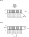
- Figure 4 shows the photoconductive transducer according to the invention operating as a source of terahertz radiation. It comprises-a laser L, which has been represented symbolically by a solid arrow, emitting at a defined wavelength, the second electrode E2 being transparent at the aforementioned wavelength. The laser is arranged so as to irradiate, through the second electrode E2, the array of nano-columns C, which are embedded in the resist R, with the aforementioned array being referenced by R + C in Figure 4 .
- the arrangement of the structure with the conversion medium being composed of the resist layer and the array of nano-columns placed between the two planar and parallel electrodes, allows for the creation of a uniform electric field by subjecting the two electrodes, E1 and E2, to a potential difference V of a few volts.
- this potential difference is capable of creating very strong electric fields.
- the order of magnitude of these fields is of 100 kV/cm.
- the applied voltages are DC or AC.
- the created electric field accelerates uniformly the charge carriers generated by the absorption of the laser radiation.
- the uniform electric field allows the number of carriers collected by the electrodes to be maximized and thus the generated signal to be increased. It is therefore essential for the height of the pillars to be small such that the distance travelled by these carriers is minimized. Minimum travelled distance ensures that the carriers are not lost through recombination mechanisms.
- the transducer generates terahertz radiation or picosecond electrical signals R T
- the aforementioned R T can be converted to a free space terahertz radiation through the aid of an antenna element or guided through waveguide elements towards micro- and nano- electronic circuits as shown in figure 5 .
- the references of figure 5 are identical to those of figure 4 .
- the duration, the intensity and the frequency bandwidth generated, depend on the duration of the laser source, on its power, on its wavelength and on the potential difference V applied between the electrodes E1 and E2.
- Figure 6 shows the photoconductive transducer according to the invention operating as a detector of terahertz radiation.
- the terahertz radiation accelerates the electrons, which flow between the two electrodes E1 and E2.
- the process for producing the transducer structure comprises of the steps described below.
- Another advantage is that the same structure may be used as a source of terahertz radiation and as a receiver of the same radiation.
- the transducer can be used on-chip in micro and nano-electronic circuits.
- This transducer may be employed in a wide range of applications covering the fields of security, of biological or chemical detection, of quality control, of telecommunications, of electronics and quantum electronics.
Landscapes
- Light Receiving Elements (AREA)
- Investigating Or Analysing Materials By Optical Means (AREA)
- Chemical & Material Sciences (AREA)
- Composite Materials (AREA)
Abstract
Description
- The field of the invention is the field of sources for generating or for detecting radiation at very high frequencies and/or electrical pulses of very short durations, of the order of a picosecond or shorter than a picosecond. One of the preferred applications of the invention is the development of high-efficiency terahertz sources.
- Terahertz radiation has various fields of application that are particularly related to its high penetration power into most materials. For example, the fields of application for this invention may be security, detection, quality control, communications and electronic applications employing nanotechnologies. It is possible to use these sources at room temperature or at cryogenic temperatures.
- Developing this highly-efficient terahertz source is one of the encountered difficulties. One possible production technique involves converting optical radiation generated by a continuous-wave or pulsed laser into terahertz radiation and/or electrical pulses. Various transducing means are possible.
- One of the most common means is to employ an optoelectronic device, known as a photoconductive switch. The latter may generate continuous-wave terahertz radiation or picosecond electrical pulses via the following mechanism.
- A laser source-emits a continuous-wave radiation or radiation in the form of ultra-short pulses. The so-called ultra-short refers to pulses with time duration smaller than 100 femtosecond. The radiation provided by the laser source is located in the visible or in the near infrared region of the electromagnetic spectrum. The light provided by the laser source is absorbed by a semiconducting material, such as gallium arsenide (GaAs) or indium gallium arsenide (InGaAs). By means of optical absorption, charge carriers are generated in the semiconductor and subsequently collected by metal contacts herein called electrodes, thus creating an electrical signal. Herein, the process of charge carrier generation by means of optical absorption will be referred to as photo-generation.
- The temporal duration and frequency of this signal depend on the frequency and duration of the light provided by the laser source. The very high dynamic range of the optoelectronic device allows electrical signals to be generated in the gigahertz or terahertz frequency bands.
- The main drawback of the existing technology is its low conversion efficiency, which makes it unsuitable for applications that require a certain terahertz power or for systems and applications that are required to operate in a cryogenic environment.
- The conversion efficiency is defined as the ratio between the optical power delivered by the laser source and the terahertz power delivered by the optoelectronic device. This efficiency is the product of two factors. The first factor is related with the absorption efficiency of the laser light by the semiconductor. The absorption efficiency is generally low.
- The second factor is related to the collection efficiency of the photo-generated charge carriers by the electrodes of the optoelectronic device. This efficiency is also low. A certain number of technical solutions for improving these two factors have been proposed.
- The publication by Nezih T. Yardimci et al. entitled "High-Power Terahertz Generation Using Large-Area Plasmonic Photoconductive Emitters" published in IEEE Transactions on Terahertz Science and Technology, Vol. 5, N° 2, March 2015 pp.223-229 and patent application
WO2013/112608 entitled "Photoconductive device with plasmonic electrodes", describe a photoconductive device comprising the following components. A semiconductor substrate, an antenna assembly and a photoconductive assembly that is made out of one or more plasmonic contact electrodes positioned on the semiconductor substrate. This photoconductive assembly is made such as to improve the overall efficiency of the photoconductor device by increasing the laser absorption efficiency in the photo-absorbing regions of the semiconductor substrate through plasmonic resonances. This device only improves the laser absorption efficiency. - The publication by Shang-Hua Yang et al. entitled "7.5% Optical-to-Terahertz Conversion Efficiency Offered by Photoconductive Emitters With Three-Dimensional Plasmonic Contact Electrodes", published in IEEE Transactions on Terahertz Science and Technology, Vol. 4, N° 5, September 2014 pp.575-581 proposes a similar photoconductive device comprising an array composed of parallel rows of plasmonic contact electrodes.
- The publication by Nezih Tolga Yardimci et al. entitled "A High-Power Broadband Terahertz Source Enabled by Three-Dimensional Light Confinement in a Plasmonic Nanocavity" published in Scientific Reports, 7(1), pp.4166 describes a device similar to the preceding ones but it comprises an additional distributed Bragg reflector as part of the photo-absorbing semiconductor to facilitate further increase of the laser absorption.
- The publication by Burford et al. entitled "Computational modeling of plasmonic thin-film terahertz photoconductive antennas" published in the Journal of the Optical Society of America B, 33(4), pp.748-759 describes a photoconductive device comprising a thin plasmonic array of nanodiscs placed on the contact electrodes.
- Lastly, the publication by Peytavit et al. entitled "Low-Temperature-Grown GaAs Photoconductor with High Dynamic Responsivity in the Millimeter Wave Range" published in Applied Physics Express 4 (2011) 104101 and French patent application
FR 2 949 905 - None of these publications allows for both, high laser absorption efficiency and a satisfactory collection efficiency of the generated carriers to be achieved. One aim of the invention is to significantly improve these two efficiencies using a single and simple structure that combines the advantages of a parallel-electrode device and of plasmonic/photonic structures.
- More precisely, one subject of the invention is a photoconductive transducer intended to generate or to detect waves and signals in the terahertz frequency domain or in the picosecond pulse domain. The said transducer is comprised of a structure that includes in the following order: First a planar electrode, then an array of photo-absorbing nano-columns embedded in a layer of resist and finally a second planar electrode parallel to the first electrode. The layer of resist has a thickness in the range between 100 nanometres and 400 nanometres. The aforementioned nano-columns are made of a photo-absorbing semiconductor material and are embedded in the layer of resist. The nano-columns are positioned perpendicular to the two planes defined by the electrodes. The height of each nano-column is equal to the thickness of the resist layer. The width of the nano-columns is in the range between 100 nanometres and 400 nanometres and the distance between two consecutive nano-columns is between 300 nanometres and 500 nanometres. The nano-columns are made of a III-V semiconductor and each column has at one end a metal contact that allows the electrical connection to the second electrode.
- It should be appreciated that, the structure is comprised of an area between 1 µm2 and 1000 µm2.
- It should be appreciated that, the second electrode is transparent in a defined spectral band.
- It should be appreciated that, the resist is transparent and thus non-absorbing in the aforementioned defined spectral band.
- It should be appreciated that, the second electrode is made of indium-tin oxide.
- It should be appreciated that, the cross section of the nano-columns is rectangular or circular or polygonal.
- It should be appreciated that, the material of the nano-columns is a III-V semiconductors, such as gallium arsenide or indium-gallium arsenide or indium phosphide.
- It should be appreciated that, the resist is a negative epoxy photoresist.
- It should be appreciated that, the aforementioned transducer which is operated by a laser that emits at a defined wavelength and defined by the second electrode which is transparent at the aforementioned wavelength, the laser being arranged so as to irradiate the array of nano-columns through the aforementioned second electrode, the width and height of the nano-columns and the distance separating two adjacent nano-columns being similar to the aforementioned wavelength, the two electrodes being subjected to a potential difference of a few volts, the transducer generating terahertz radiation with the duration, the intensity and the frequency bandwidth of which is dependent on the duration of the laser emission, on its power, on its wavelength and on the voltage potential between the aforementioned electrodes.
- It should be appreciated that, the transducer is also used as a detector of waves and signals in the terahertz frequency domain or in the picosecond pulse domain.
- It should be appreciated that, the transducer is also used as a source or generator for picosecond electrical pulses and used on-chip in micro- and nano-electronic circuits.
- It should be appreciated that, the transducer is also used as a source or generator for THz continuous waves and used on-chip in micro- and nano- electronic circuits.
- It should be appreciated that, the transducer is also used both at ambient temperatures and/or cryogenic temperatures.
- The invention also relates to a process for producing a photoconductive transducer comprising-a structure that includes a first planar electrode, the nano-columns embedded in a layer of resist and a second planar electrode parallel to the first electrode. The production of the assembly, being arranged as defined above, comprises the following steps:
- etching the array of nano-columns in a substrate made of III-V semiconductor;
- depositing a metal layer on the upper surface of the columns and on the lower surface of the substrate that bears the columns. The upper and lower metal layers will thus constitute the metal contacts and act as planar electrodes;
- spin coating of a layer of negative epoxy photoresist to cover completely the array of nano-columns;
- exposing the layer of resist;
- polishing or etching the layer of resist until the metal contacts of the top of the nano-columns appear;
- depositing a transparent metal layer on top of the layer of resist, so as to connect the various metal contacts at the ends of the nano-columns.
- Other features, details and advantages of the invention will become apparent upon reading the description, which is given with reference to the appended drawings, which are given by way of example and show, respectively:
- [
Fig.1 ] an illustration of a top view of the structure of a photoconductive transducer according to the invention; - [
Fig.2 ] an illustration of a partial perspective view of the nano-columns comprising the photoconductive transducer according to the invention; - [
Fig.3 ] an illustration of a cross-sectional view of a nano-column according to the invention; - [
Fig.4 ] an illustration of a first embodiment of the photoconductive transducer, employed as a source of terahertz radiation; - [
Fig.5 ] an illustration of a second embodiment of the photoconductive transducer, employed as a source of terahertz radiation; - [
Fig.6 ] an illustration of a third embodiment of the photoconductive transducer, employed as a receiver of terahertz radiation. - The photoconductive transducer, according to the invention, may operate either as an emitter or as a receiver of waves in the terahertz frequency domain or in the picosecond pulse domain. Excluding a few details, the structure used for these two applications is the same.
- The photoconductive transducer, according to the invention, may also operate as a source for THz frequency waves or electrical signals with picosecond time duration for micro- or nano-electronic circuits.
- The core of the transducer comprises a structure including, in this order, the following three elements:
- a first planar electrode,
- a layer of resist comprising-an embedded array of identical nano-columns placed perpendicular to the plane defined by the first electrode. The distances between two adjacent columns is constant,
- a second planar electrode parallel to the first planar electrode.
- The area of the structure is between 1 µm2 and 1000 µm2, depending on the use of the transducer.
-
Figure 1 shows a top view of the nano-column array C placed on top of the first electrode E1.Figure 2 shows a partial perspective view of the nano-columns C of the photoconductive transducer according to the invention. In the case ofFigure 2 , the columns are of rectangular cross section. The cross section of the columns may also be circular or polygonal. - When the transducer is used as an emitter, it is used in combination with a laser source that emits at a defined wavelength. This wavelength is generally located in the visible or in the near infrared region of the electromagnetic spectrum. In this case, certain characteristics of the structure depend on this wavelength.
- The first electrode is formed by a conductive deposit that may be made of gold or titanium or silver or aluminum.
- The second electrode E2 must be transparent at the aforementioned wavelength so as to let the incident laser radiation penetrate into the structure. To this end, the second electrode may be formed by depositing a layer of indium-tin oxide, which is transparent between 300 nanometres and 1000 nanometres.
- The thickness of the second electrode E2 is specific to the aforementioned wavelength and must be such that it forms an anti-reflection coating for the particular wavelength.
- In the same way, the resist R must also be transparent at the wavelength of the laser source. For example, it is possible to use a negative photoresist, such as the resist known as SU-8, which is commonly used in the fabrication of microsystems of this type and of which there are various variants. Other types of transparent resists are, of course, possible. The layer of resist generally has a thickness comprised between 100 nanometres and 400 nanometres.
- The height of the nano-columns is equal to the height of the layer of resist. The width of the columns and the distance separating two adjacent columns are adapted to the wavelength of the laser and to the refractive index of the resist.
- By optimizing the spatial dimensions of the nano-columns with respect to the spatial dimension of the laser wavelength, the absorption of the laser light is maximized, with this being the desired aim. The length and width of each nano-column are such that the laser is absorbed by excitation of plasmonic resonances at the upper and lower surfaces of the structure. In addition, guided optical photonic modes, which propagate through the heterogeneous layer consisting of the polymer resist and of the array of nano-columns, will also be excited. Furthermore, a resonant cavity mode will also be excited inside the nano-column and in the vertical direction between the two electrodes. Generally, the width of the columns is in the range between 100 nanometres and 400 nanometres.
- The pitch of the array of the nano-columns, which corresponds to the distance between two successive columns, is responsible for the excitation of collective photonic resonances described above. This is due to the periodic arrangement of the nano-columns which diffract efficiently the laser light into the interior of the heterogeneous layer. The distance between two columns is between 300 nanometres and 500 nanometres. By combining plasmonic and photonic effects, it is possible to obtain an absorption higher than 95%.
- The material of the columns must be optimized to obtain the best possible picosecond pulse. Materials with very fast carrier response times, i.e. with very fast carrier dynamics, must therefore be used. To give an order of magnitude, it is preferable for this time to be shorter than 10 picoseconds. For example, the nano-columns can be made of specially treated III-V semiconductors such as gallium arsenide or gallium indium arsenide or indium phosphide.
- Each column C bears a contact on the top end that is made of a conductive material that is identical to that of the first electrode and that ensures electrical continuity with the transparent second electrode.
-
Figure 3 shows a cross-sectional view of a nano-column C according to the invention. It is encircled by a resist R. It comprises-an electrical contact CE. The resist R is situated between the two electrodes E1 and E2. -
Figure 4 shows the photoconductive transducer according to the invention operating as a source of terahertz radiation. It comprises-a laser L, which has been represented symbolically by a solid arrow, emitting at a defined wavelength, the second electrode E2 being transparent at the aforementioned wavelength. The laser is arranged so as to irradiate, through the second electrode E2, the array of nano-columns C, which are embedded in the resist R, with the aforementioned array being referenced by R + C inFigure 4 . - The arrangement of the structure with the conversion medium being composed of the resist layer and the array of nano-columns placed between the two planar and parallel electrodes, allows for the creation of a uniform electric field by subjecting the two electrodes, E1 and E2, to a potential difference V of a few volts.
- Because of the very small distance separating the two electrodes, this potential difference is capable of creating very strong electric fields. The order of magnitude of these fields is of 100 kV/cm. Depending on the application, the applied voltages are DC or AC.
- The created electric field accelerates uniformly the charge carriers generated by the absorption of the laser radiation. The uniform electric field allows the number of carriers collected by the electrodes to be maximized and thus the generated signal to be increased. It is therefore essential for the height of the pillars to be small such that the distance travelled by these carriers is minimized. Minimum travelled distance ensures that the carriers are not lost through recombination mechanisms.
- The transducer generates terahertz radiation or picosecond electrical signals RT The aforementioned RT can be converted to a free space terahertz radiation through the aid of an antenna element or guided through waveguide elements towards micro- and nano- electronic circuits as shown in
figure 5 . The references offigure 5 are identical to those offigure 4 . The duration, the intensity and the frequency bandwidth generated, depend on the duration of the laser source, on its power, on its wavelength and on the potential difference V applied between the electrodes E1 and E2. -
Figure 6 shows the photoconductive transducer according to the invention operating as a detector of terahertz radiation. The terahertz radiation accelerates the electrons, which flow between the two electrodes E1 and E2. - For example, the process for producing the transducer structure, according to the invention, comprises of the steps described below.
- Step 1: etching the array of columns in a substrate made of III-V semiconductors such as gallium arsenide or indium-gallium arsenide or indium phosphide;
- Step 2: depositing a metal layer on the upper surface of the columns and on the lower surface of the substrate that bears the columns. The metal layers will constitute the metal contacts. This operation may be carried out at low pressure, i.e. at a pressure below 10-6 millibars and with a slow evaporation rate, the order of magnitude of the evaporation rate being 0.5 nm/s. The deposited metal may be made of gold or silver or aluminum or titanium. It is essential, in this operation, that there is no contact between the bottom metal layer, which serves as first electrode, and the metal layer on the upper surface of the nano-columns, which connects to the second electrode;
- Step 3: spin coating a layer of negative epoxy photoresist such as SU-8 and cover completely the array of nano-columns. The deposited thickness can be for homogeneity three times larger than the height of the nano-columns;
- Step 4: exposing the layer of resist with an electron beam or UV lithography;
- Step 5: polishing or etching the layer of resist until the metal contacts at the top of the nano-columns appear;
- Step 6: depositing a transparent metal layer on the layer of resist so as to connect the various metal contacts. This layer may be made of indium-tin oxide. The thickness of the latter layer is in the range between 100 nanometers and 300 nanometers, depending on the wavelength of the laser source.
- The following are the main advantages of the photoconductive transducer according to the invention:
Its three-dimensional structure allows high efficiencies to be obtained, much higher than those obtained with prior-art devices. An improvement of a factor of 10 in efficiency is thus obtained over current transducers. - Moreover, its "vertical" structure composed of the array of nano-columns sandwiched between two electrodes allows this efficiency to be further optimized.
- Another advantage is that the same structure may be used as a source of terahertz radiation and as a receiver of the same radiation.
- The transducer can be used on-chip in micro and nano-electronic circuits.
- This transducer may be employed in a wide range of applications covering the fields of security, of biological or chemical detection, of quality control, of telecommunications, of electronics and quantum electronics.
- Its architecture allows it to operate at room temperature and at cryogenic temperatures for ultra-fast electronic switching applications. Thus, it is possible to use it in quantum technologies. It is possible to use it as an ultra-fast source for inspecting, triggering or driving qubits for quantum computers.
Claims (14)
- Photoconductive transducer intended to generate or detect waves in the terahertz frequency domain or in the picosecond pulse domain, characterized by the photoconductive transducer, comprises-a three-dimensional structure that includes, in this order, a first planar electrode (E1), an array of identical nano-columns (C) embedded in a layer of resist (R) and a second planar electrode (E2) parallel to the first planar electrode, the height of the nano-columns as well as the thickness of the resist ranging between 100 nanometres and 400 nanometres, the width of the nano-columns being between 100 nanometres and 400 nanometres, the distance between two consecutive nano-columns being between 300 nanometres and 500 nanometres, the nano-columns made of a III-V semiconductor and the top part of each nano-column comprising a metal contact (CE) that is electrically connected to the second electrode.
- Photoconductive transducer according to Claim 1, characterized by the area of the three-dimensional structure is between 1 µm2 and 1000 µm2.
- Photoconductive transducer according to one of the preceding claims, characterized by the second electrode is transparent in a defined spectral band.
- Photoconductive transducer according to one of the preceding claims, characterized by the resist is transparent in a defined spectral band.
- Photoconductive transducer according to Claim 1, characterized by the second electrode is made of indium-tin oxide.
- Photoconductive transducer according to one of the preceding claims, characterized by the cross section of the nano-columns is rectangular or circular or polygonal.
- Photoconductive transducer according to one of the preceding claims, characterized by the material of the nano-columns is made from III-V semiconductors, such as gallium arsenide or indium-gallium arsenide or indium phosphide.
- Photoconductive transducer according to one of the preceding claims, characterized by the resist is a negative epoxy photoresist.
- Photoconductive transducer according to one of the preceding claims, characterized by the transducer which is operated by a laser (L) that emits at a defined wavelength, the second electrode being transparent at the aforementioned wavelength, the laser being arranged so as to irradiate the array of columns through the aforementioned second electrode, the width and height of the nano-columns and the distance separating two adjacent columns being similar to the aforementioned wavelength, the two electrodes being subjected to a potential difference of a few volts, the transducer generating terahertz radiation with the duration, the intensity and the frequency bandwidth of which is dependent on the duration of the laser emission, on its power on its wavelength and on the voltage potential between the aforementioned electrodes.
- Photoconductive transducer according to one of the preceding claims, characterized by the transducer is used as a detector of waves in the terahertz frequency domain or in the picosecond pulse domain for electrical signals.
- Photoconductive transducer according to the preceding claims, characterized by the transducer is used as a source or generator for picosecond electrical pulses and used on-chip in micro- and nano- electronic circuits.
- Photoconductive transducer according to the preceding claims, characterized by the transducer is used as a source or generator for THz continuous waves and used on-chip in micro- and nano- electronic circuits.
- Photoconductive transducer according to the preceding claims, characterized by the transducer is used both at ambient temperatures and/or cryogenic temperatures.
- Process for producing a photoconductive transducer according to one of Claims 1 to 13, characterized by the production of the three-dimensional structure comprises the following steps:- etching the array of nano-columns in a substrate made of III-V semiconductor;- depositing a metal layer on the upper surface of the nano-columns and on the lower surface of the substrate that bears the nano-columns, the top of the nano-columns thus comprising of a metal contact;- spin coating a layer of negative epoxy photoresist to cover the aforementioned array of columns;- exposing the aforementioned layer of resist;- polishing or etching the aforementioned layer of resist until the metal contacts at the top-end of the nano-columns appear;- depositing a transparent metal layer on the layer of resist so as to connect the various metal contacts.
Priority Applications (7)
| Application Number | Priority Date | Filing Date | Title |
|---|---|---|---|
| LTEP19306646.1T LT3836232T (en) | 2019-12-13 | 2019-12-13 | THREE-DIMENSIONAL PHOTOCONDUCTIVE TRANSDUCER FOR TERAHERTZ FREQUENCY SIGNALS OR PICOSECOND ELECTRICAL IMPULSES |
| ES19306646T ES2909787T3 (en) | 2019-12-13 | 2019-12-13 | Three-dimensional photoconductive transducer for terahertz signals or picosecond electrical pulses |
| EP19306646.1A EP3836232B1 (en) | 2019-12-13 | 2019-12-13 | Three-dimensional photoconductive transducer for terahertz signals or picosecond electrical pulses |
| US17/782,987 US12206039B2 (en) | 2019-12-13 | 2020-12-10 | Three-dimensional photoconductive transducer for terahertz signals or picosecond electrical pulses |
| JP2022535967A JP7638994B2 (en) | 2019-12-13 | 2020-12-10 | Three-dimensional photoconductive transducer for terahertz signals or picosecond electrical pulses |
| CN202080086302.9A CN115244716B (en) | 2019-12-13 | 2020-12-10 | Three-dimensional photoconductive transducer for terahertz signals or picosecond electrical pulses |
| PCT/EP2020/085625 WO2021116339A1 (en) | 2019-12-13 | 2020-12-10 | Three-dimensional photoconductive transducer for terahertz signals or picosecond electrical pulses |
Applications Claiming Priority (1)
| Application Number | Priority Date | Filing Date | Title |
|---|---|---|---|
| EP19306646.1A EP3836232B1 (en) | 2019-12-13 | 2019-12-13 | Three-dimensional photoconductive transducer for terahertz signals or picosecond electrical pulses |
Publications (2)
| Publication Number | Publication Date |
|---|---|
| EP3836232A1 true EP3836232A1 (en) | 2021-06-16 |
| EP3836232B1 EP3836232B1 (en) | 2022-01-12 |
Family
ID=69411168
Family Applications (1)
| Application Number | Title | Priority Date | Filing Date |
|---|---|---|---|
| EP19306646.1A Active EP3836232B1 (en) | 2019-12-13 | 2019-12-13 | Three-dimensional photoconductive transducer for terahertz signals or picosecond electrical pulses |
Country Status (7)
| Country | Link |
|---|---|
| US (1) | US12206039B2 (en) |
| EP (1) | EP3836232B1 (en) |
| JP (1) | JP7638994B2 (en) |
| CN (1) | CN115244716B (en) |
| ES (1) | ES2909787T3 (en) |
| LT (1) | LT3836232T (en) |
| WO (1) | WO2021116339A1 (en) |
Citations (4)
| Publication number | Priority date | Publication date | Assignee | Title |
|---|---|---|---|---|
| FR2949905A1 (en) | 2009-09-09 | 2011-03-11 | Centre Nat Rech Scient | PHOTODETECTOR, PHOTOMELANGER AND THEIR APPLICATION TO TERAHERTZ RADIATION GENERATION. |
| WO2013112608A1 (en) | 2012-01-23 | 2013-08-01 | The Regents Of The University Of Michigan | Photoconductive device with plasmonic electrodes |
| US20140175283A1 (en) * | 2011-02-14 | 2014-06-26 | Centre National De La Recherche Scientifique-Cnrs | Terahertz detection cell |
| CN108417976A (en) * | 2018-02-05 | 2018-08-17 | 天津大学 | Gallium arsenide nanocolumn array terahertz wave emitting device and manufacturing method |
Family Cites Families (9)
| Publication number | Priority date | Publication date | Assignee | Title |
|---|---|---|---|---|
| US7335908B2 (en) | 2002-07-08 | 2008-02-26 | Qunano Ab | Nanostructures and methods for manufacturing the same |
| JP5369366B2 (en) * | 2006-02-16 | 2013-12-18 | ソニー株式会社 | Photoelectric conversion element, semiconductor device and electronic device |
| JP2009088292A (en) * | 2007-09-28 | 2009-04-23 | Fujifilm Corp | Photoelectric conversion device, imaging device, and optical sensor |
| JP2010045157A (en) | 2008-08-12 | 2010-02-25 | Kansai Electric Power Co Inc:The | Terahertz electromagnetic wave radiation element and terahertz electromagnetic wave generation method |
| JP5398773B2 (en) * | 2011-04-07 | 2014-01-29 | 富士フイルム株式会社 | Radiation detector |
| US20140175546A1 (en) | 2012-11-06 | 2014-06-26 | The Regents Of The University Of California | Plasmonically enhanced electro-optic devices and methods of production |
| US9136421B2 (en) * | 2013-01-15 | 2015-09-15 | Electronics And Telecommunications Research Institute | Wide area array type photonic crystal photomixer for generating and detecting broadband terahertz wave |
| WO2017083840A1 (en) * | 2015-11-13 | 2017-05-18 | Uvic Industry Partnerships Inc. | Plasmon-enhanced below bandgap photoconductive terahertz generation and detection |
| US11749694B1 (en) * | 2019-09-03 | 2023-09-05 | National Technology & Engineering Solutions Of Sandia, Llc | Photoconductive metasurface-based ultrafast device |
-
2019
- 2019-12-13 LT LTEP19306646.1T patent/LT3836232T/en unknown
- 2019-12-13 EP EP19306646.1A patent/EP3836232B1/en active Active
- 2019-12-13 ES ES19306646T patent/ES2909787T3/en active Active
-
2020
- 2020-12-10 JP JP2022535967A patent/JP7638994B2/en active Active
- 2020-12-10 US US17/782,987 patent/US12206039B2/en active Active
- 2020-12-10 WO PCT/EP2020/085625 patent/WO2021116339A1/en not_active Ceased
- 2020-12-10 CN CN202080086302.9A patent/CN115244716B/en active Active
Patent Citations (4)
| Publication number | Priority date | Publication date | Assignee | Title |
|---|---|---|---|---|
| FR2949905A1 (en) | 2009-09-09 | 2011-03-11 | Centre Nat Rech Scient | PHOTODETECTOR, PHOTOMELANGER AND THEIR APPLICATION TO TERAHERTZ RADIATION GENERATION. |
| US20140175283A1 (en) * | 2011-02-14 | 2014-06-26 | Centre National De La Recherche Scientifique-Cnrs | Terahertz detection cell |
| WO2013112608A1 (en) | 2012-01-23 | 2013-08-01 | The Regents Of The University Of Michigan | Photoconductive device with plasmonic electrodes |
| CN108417976A (en) * | 2018-02-05 | 2018-08-17 | 天津大学 | Gallium arsenide nanocolumn array terahertz wave emitting device and manufacturing method |
Non-Patent Citations (5)
| Title |
|---|
| BURFORD ET AL.: "Computational modeling of plasmonic thin-film terahertz photoconductive antennas", JOURNAL OF THE OPTICAL SOCIETY OF AMERICA B, vol. 33, no. 4, pages 748 - 759 |
| NEZIH T. YARDIMCI ET AL.: "High-Power Terahertz Generation Using Large-Area Plasmonic Photoconductive Emitters", IEEE TRANSACTIONS ON TERAHERTZ SCIENCE AND TECHNOLOGY, vol. 5, no. 2, March 2015 (2015-03-01), pages 223 - 229, XP011574237, DOI: 10.1109/TTHZ.2015.2395417 |
| NEZIH TOLGA YARDIMCI ET AL.: "A High-Power Broadband Terahertz Source Enabled by Three-Dimensional Light Confinement in a Plasmonic Nanocavity", SCIENTIFIC REPORTS, vol. 7, no. 1, pages 4166 |
| PEYTAVIT ET AL.: "Low-Temperature-Grown GaAs Photoconductor with High Dynamic Responsivity in the Millimeter Wave Range", APPLIED PHYSICS EXPRESS, vol. 4, 2011, pages 104101 |
| SHANG-HUA YANG ET AL.: "7.5% Optical-to-Terahertz Conversion Efficiency Offered by Photoconductive Emitters With Three-Dimensional Plasmonic Contact Electrodes", IEEE TRANSACTIONS ON TERAHERTZ SCIENCE AND TECHNOLOGY, vol. 4, no. 5, September 2014 (2014-09-01), pages 575 - 581, XP011557229, DOI: 10.1109/TTHZ.2014.2342505 |
Also Published As
| Publication number | Publication date |
|---|---|
| EP3836232B1 (en) | 2022-01-12 |
| ES2909787T3 (en) | 2022-05-10 |
| CN115244716A (en) | 2022-10-25 |
| US20230026900A1 (en) | 2023-01-26 |
| LT3836232T (en) | 2022-07-11 |
| WO2021116339A1 (en) | 2021-06-17 |
| JP7638994B2 (en) | 2025-03-04 |
| JP2023505716A (en) | 2023-02-10 |
| CN115244716B (en) | 2024-10-18 |
| US12206039B2 (en) | 2025-01-21 |
Similar Documents
| Publication | Publication Date | Title |
|---|---|---|
| US11231318B2 (en) | Photoconductive detector device with plasmonic electrodes | |
| US8581784B2 (en) | THz antenna array, system and method for producing a THz antenna array | |
| US10120263B2 (en) | Low-duty-cycle continuous-wave photoconductive terahertz imaging and spectroscopy systems | |
| US20140197425A1 (en) | Wide area array type photonic crystal photomixer for generating and detecting broadband terahertz wave | |
| US7608814B2 (en) | Optical structure for localising an electromagnetic field and detector or emitter device including such a structure | |
| US12206039B2 (en) | Three-dimensional photoconductive transducer for terahertz signals or picosecond electrical pulses | |
| CN117650190B (en) | Plasmon electrode photoelectric detector suitable for unpolarized light | |
| US12498615B2 (en) | Systems and methods for wavelength conversion through plasmon-coupled surface states | |
| Lee et al. | High efficiency interdigitated Terahertz photoconductive antenna integrated with cylindrical lens array | |
| Lu et al. | Plasmonics‐enhanced photoconductive terahertz devices | |
| Gorodetsky et al. | Quantum dot photoconductive antenna-based compact setups for terahertz spectroscopy and imaging | |
| Yardimci et al. | High-power, broadband terahertz radiation from large area plasmonic photoconductive emitters operating at telecommunication optical wavelengths | |
| Yardimci et al. | 1550 nm Large-area plasmonic photoconductive terahertz sources | |
| WO2013068516A1 (en) | Photomixer for terahertz electromagnetic wave emission comprising quantum dots in a laser cavity | |
| Yardimci et al. | Plasmonics enhanced terahertz radiation from large area photoconductive emitters | |
| Yardimci et al. | Telecommunication compatible terahertz emitters based on plasmonic nano-antenna arrays | |
| Lampin et al. | High efficiency optoelectronic terahertz sources | |
| Mastrangelo et al. | Purcell enhanced electroluminescence of a unipolar light emitting quantum device at 10 micron | |
| Yardimci et al. | Terahertz radiation enhancement in large-area photoconductive sources by using plasmonic nanoantennas | |
| Yardimci et al. | Boosting radiation efficiency of photoconductive nano-antennas through 3D light confinement | |
| Belkin et al. | THz quantum cascade lasers for operation above cryogenic temperatures | |
| Yardimci et al. | Large area plasmonic photoconductive emitters for generating high power broadband terahertz radiation | |
| Yardimci et al. | Highly efficient photoconductive terahertz generation through photon trapping | |
| Takahashi et al. | Mid-infrared and THz coherent sources using semiconductor-based materials | |
| Berry et al. | Enhancing optical-to-terahertz conversion efficiency by using plasmonic photoconductive emitters |
Legal Events
| Date | Code | Title | Description |
|---|---|---|---|
| PUAI | Public reference made under article 153(3) epc to a published international application that has entered the european phase |
Free format text: ORIGINAL CODE: 0009012 |
|
| STAA | Information on the status of an ep patent application or granted ep patent |
Free format text: STATUS: THE APPLICATION HAS BEEN PUBLISHED |
|
| AK | Designated contracting states |
Kind code of ref document: A1 Designated state(s): AL AT BE BG CH CY CZ DE DK EE ES FI FR GB GR HR HU IE IS IT LI LT LU LV MC MK MT NL NO PL PT RO RS SE SI SK SM TR |
|
| STAA | Information on the status of an ep patent application or granted ep patent |
Free format text: STATUS: REQUEST FOR EXAMINATION WAS MADE |
|
| 17P | Request for examination filed |
Effective date: 20210719 |
|
| RBV | Designated contracting states (corrected) |
Designated state(s): AL AT BE BG CH CY CZ DE DK EE ES FI FR GB GR HR HU IE IS IT LI LT LU LV MC MK MT NL NO PL PT RO RS SE SI SK SM TR |
|
| GRAP | Despatch of communication of intention to grant a patent |
Free format text: ORIGINAL CODE: EPIDOSNIGR1 |
|
| STAA | Information on the status of an ep patent application or granted ep patent |
Free format text: STATUS: GRANT OF PATENT IS INTENDED |
|
| INTG | Intention to grant announced |
Effective date: 20210930 |
|
| GRAS | Grant fee paid |
Free format text: ORIGINAL CODE: EPIDOSNIGR3 |
|
| GRAA | (expected) grant |
Free format text: ORIGINAL CODE: 0009210 |
|
| STAA | Information on the status of an ep patent application or granted ep patent |
Free format text: STATUS: THE PATENT HAS BEEN GRANTED |
|
| AK | Designated contracting states |
Kind code of ref document: B1 Designated state(s): AL AT BE BG CH CY CZ DE DK EE ES FI FR GB GR HR HU IE IS IT LI LT LU LV MC MK MT NL NO PL PT RO RS SE SI SK SM TR |
|
| REG | Reference to a national code |
Ref country code: GB Ref legal event code: FG4D |
|
| REG | Reference to a national code |
Ref country code: CH Ref legal event code: EP |
|
| REG | Reference to a national code |
Ref country code: DE Ref legal event code: R096 Ref document number: 602019010860 Country of ref document: DE |
|
| REG | Reference to a national code |
Ref country code: IE Ref legal event code: FG4D |
|
| REG | Reference to a national code |
Ref country code: AT Ref legal event code: REF Ref document number: 1462951 Country of ref document: AT Kind code of ref document: T Effective date: 20220215 |
|
| REG | Reference to a national code |
Ref country code: ES Ref legal event code: FG2A Ref document number: 2909787 Country of ref document: ES Kind code of ref document: T3 Effective date: 20220510 |
|
| REG | Reference to a national code |
Ref country code: NL Ref legal event code: MP Effective date: 20220112 |
|
| REG | Reference to a national code |
Ref country code: AT Ref legal event code: MK05 Ref document number: 1462951 Country of ref document: AT Kind code of ref document: T Effective date: 20220112 |
|
| PG25 | Lapsed in a contracting state [announced via postgrant information from national office to epo] |
Ref country code: NL Free format text: LAPSE BECAUSE OF FAILURE TO SUBMIT A TRANSLATION OF THE DESCRIPTION OR TO PAY THE FEE WITHIN THE PRESCRIBED TIME-LIMIT Effective date: 20220112 |
|
| PG25 | Lapsed in a contracting state [announced via postgrant information from national office to epo] |
Ref country code: SE Free format text: LAPSE BECAUSE OF FAILURE TO SUBMIT A TRANSLATION OF THE DESCRIPTION OR TO PAY THE FEE WITHIN THE PRESCRIBED TIME-LIMIT Effective date: 20220112 Ref country code: RS Free format text: LAPSE BECAUSE OF FAILURE TO SUBMIT A TRANSLATION OF THE DESCRIPTION OR TO PAY THE FEE WITHIN THE PRESCRIBED TIME-LIMIT Effective date: 20220112 Ref country code: PT Free format text: LAPSE BECAUSE OF FAILURE TO SUBMIT A TRANSLATION OF THE DESCRIPTION OR TO PAY THE FEE WITHIN THE PRESCRIBED TIME-LIMIT Effective date: 20220512 Ref country code: NO Free format text: LAPSE BECAUSE OF FAILURE TO SUBMIT A TRANSLATION OF THE DESCRIPTION OR TO PAY THE FEE WITHIN THE PRESCRIBED TIME-LIMIT Effective date: 20220412 Ref country code: HR Free format text: LAPSE BECAUSE OF FAILURE TO SUBMIT A TRANSLATION OF THE DESCRIPTION OR TO PAY THE FEE WITHIN THE PRESCRIBED TIME-LIMIT Effective date: 20220112 Ref country code: BG Free format text: LAPSE BECAUSE OF FAILURE TO SUBMIT A TRANSLATION OF THE DESCRIPTION OR TO PAY THE FEE WITHIN THE PRESCRIBED TIME-LIMIT Effective date: 20220412 |
|
| PG25 | Lapsed in a contracting state [announced via postgrant information from national office to epo] |
Ref country code: PL Free format text: LAPSE BECAUSE OF FAILURE TO SUBMIT A TRANSLATION OF THE DESCRIPTION OR TO PAY THE FEE WITHIN THE PRESCRIBED TIME-LIMIT Effective date: 20220112 Ref country code: LV Free format text: LAPSE BECAUSE OF FAILURE TO SUBMIT A TRANSLATION OF THE DESCRIPTION OR TO PAY THE FEE WITHIN THE PRESCRIBED TIME-LIMIT Effective date: 20220112 Ref country code: GR Free format text: LAPSE BECAUSE OF FAILURE TO SUBMIT A TRANSLATION OF THE DESCRIPTION OR TO PAY THE FEE WITHIN THE PRESCRIBED TIME-LIMIT Effective date: 20220413 Ref country code: FI Free format text: LAPSE BECAUSE OF FAILURE TO SUBMIT A TRANSLATION OF THE DESCRIPTION OR TO PAY THE FEE WITHIN THE PRESCRIBED TIME-LIMIT Effective date: 20220112 Ref country code: AT Free format text: LAPSE BECAUSE OF FAILURE TO SUBMIT A TRANSLATION OF THE DESCRIPTION OR TO PAY THE FEE WITHIN THE PRESCRIBED TIME-LIMIT Effective date: 20220112 |
|
| PG25 | Lapsed in a contracting state [announced via postgrant information from national office to epo] |
Ref country code: IS Free format text: LAPSE BECAUSE OF FAILURE TO SUBMIT A TRANSLATION OF THE DESCRIPTION OR TO PAY THE FEE WITHIN THE PRESCRIBED TIME-LIMIT Effective date: 20220512 |
|
| REG | Reference to a national code |
Ref country code: DE Ref legal event code: R097 Ref document number: 602019010860 Country of ref document: DE |
|
| PG25 | Lapsed in a contracting state [announced via postgrant information from national office to epo] |
Ref country code: SM Free format text: LAPSE BECAUSE OF FAILURE TO SUBMIT A TRANSLATION OF THE DESCRIPTION OR TO PAY THE FEE WITHIN THE PRESCRIBED TIME-LIMIT Effective date: 20220112 Ref country code: SK Free format text: LAPSE BECAUSE OF FAILURE TO SUBMIT A TRANSLATION OF THE DESCRIPTION OR TO PAY THE FEE WITHIN THE PRESCRIBED TIME-LIMIT Effective date: 20220112 Ref country code: RO Free format text: LAPSE BECAUSE OF FAILURE TO SUBMIT A TRANSLATION OF THE DESCRIPTION OR TO PAY THE FEE WITHIN THE PRESCRIBED TIME-LIMIT Effective date: 20220112 Ref country code: EE Free format text: LAPSE BECAUSE OF FAILURE TO SUBMIT A TRANSLATION OF THE DESCRIPTION OR TO PAY THE FEE WITHIN THE PRESCRIBED TIME-LIMIT Effective date: 20220112 Ref country code: DK Free format text: LAPSE BECAUSE OF FAILURE TO SUBMIT A TRANSLATION OF THE DESCRIPTION OR TO PAY THE FEE WITHIN THE PRESCRIBED TIME-LIMIT Effective date: 20220112 Ref country code: CZ Free format text: LAPSE BECAUSE OF FAILURE TO SUBMIT A TRANSLATION OF THE DESCRIPTION OR TO PAY THE FEE WITHIN THE PRESCRIBED TIME-LIMIT Effective date: 20220112 |
|
| PLBE | No opposition filed within time limit |
Free format text: ORIGINAL CODE: 0009261 |
|
| STAA | Information on the status of an ep patent application or granted ep patent |
Free format text: STATUS: NO OPPOSITION FILED WITHIN TIME LIMIT |
|
| PG25 | Lapsed in a contracting state [announced via postgrant information from national office to epo] |
Ref country code: AL Free format text: LAPSE BECAUSE OF FAILURE TO SUBMIT A TRANSLATION OF THE DESCRIPTION OR TO PAY THE FEE WITHIN THE PRESCRIBED TIME-LIMIT Effective date: 20220112 |
|
| 26N | No opposition filed |
Effective date: 20221013 |
|
| PG25 | Lapsed in a contracting state [announced via postgrant information from national office to epo] |
Ref country code: IT Free format text: LAPSE BECAUSE OF FAILURE TO SUBMIT A TRANSLATION OF THE DESCRIPTION OR TO PAY THE FEE WITHIN THE PRESCRIBED TIME-LIMIT Effective date: 20220112 |
|
| REG | Reference to a national code |
Ref country code: BE Ref legal event code: MM Effective date: 20221231 |
|
| PG25 | Lapsed in a contracting state [announced via postgrant information from national office to epo] |
Ref country code: LU Free format text: LAPSE BECAUSE OF NON-PAYMENT OF DUE FEES Effective date: 20221213 |
|
| PG25 | Lapsed in a contracting state [announced via postgrant information from national office to epo] |
Ref country code: IE Free format text: LAPSE BECAUSE OF NON-PAYMENT OF DUE FEES Effective date: 20221213 |
|
| PG25 | Lapsed in a contracting state [announced via postgrant information from national office to epo] |
Ref country code: BE Free format text: LAPSE BECAUSE OF NON-PAYMENT OF DUE FEES Effective date: 20221231 |
|
| PG25 | Lapsed in a contracting state [announced via postgrant information from national office to epo] |
Ref country code: CY Free format text: LAPSE BECAUSE OF FAILURE TO SUBMIT A TRANSLATION OF THE DESCRIPTION OR TO PAY THE FEE WITHIN THE PRESCRIBED TIME-LIMIT Effective date: 20220112 |
|
| PG25 | Lapsed in a contracting state [announced via postgrant information from national office to epo] |
Ref country code: MK Free format text: LAPSE BECAUSE OF FAILURE TO SUBMIT A TRANSLATION OF THE DESCRIPTION OR TO PAY THE FEE WITHIN THE PRESCRIBED TIME-LIMIT Effective date: 20220112 Ref country code: HU Free format text: LAPSE BECAUSE OF FAILURE TO SUBMIT A TRANSLATION OF THE DESCRIPTION OR TO PAY THE FEE WITHIN THE PRESCRIBED TIME-LIMIT; INVALID AB INITIO Effective date: 20191213 |
|
| PG25 | Lapsed in a contracting state [announced via postgrant information from national office to epo] |
Ref country code: MC Free format text: LAPSE BECAUSE OF FAILURE TO SUBMIT A TRANSLATION OF THE DESCRIPTION OR TO PAY THE FEE WITHIN THE PRESCRIBED TIME-LIMIT Effective date: 20220112 |
|
| PG25 | Lapsed in a contracting state [announced via postgrant information from national office to epo] |
Ref country code: TR Free format text: LAPSE BECAUSE OF FAILURE TO SUBMIT A TRANSLATION OF THE DESCRIPTION OR TO PAY THE FEE WITHIN THE PRESCRIBED TIME-LIMIT Effective date: 20220112 Ref country code: MC Free format text: LAPSE BECAUSE OF FAILURE TO SUBMIT A TRANSLATION OF THE DESCRIPTION OR TO PAY THE FEE WITHIN THE PRESCRIBED TIME-LIMIT Effective date: 20220112 |
|
| PG25 | Lapsed in a contracting state [announced via postgrant information from national office to epo] |
Ref country code: MT Free format text: LAPSE BECAUSE OF FAILURE TO SUBMIT A TRANSLATION OF THE DESCRIPTION OR TO PAY THE FEE WITHIN THE PRESCRIBED TIME-LIMIT Effective date: 20220112 |
|
| REG | Reference to a national code |
Ref country code: DE Ref legal event code: R079 Ref document number: 602019010860 Country of ref document: DE Free format text: PREVIOUS MAIN CLASS: H01L0031090000 Ipc: H10F0030100000 |
|
| REG | Reference to a national code |
Ref country code: CH Ref legal event code: U11 Free format text: ST27 STATUS EVENT CODE: U-0-0-U10-U11 (AS PROVIDED BY THE NATIONAL OFFICE) Effective date: 20260108 |
|
| PGFP | Annual fee paid to national office [announced via postgrant information from national office to epo] |
Ref country code: LT Payment date: 20251203 Year of fee payment: 7 Ref country code: GB Payment date: 20251229 Year of fee payment: 7 |
|
| PGFP | Annual fee paid to national office [announced via postgrant information from national office to epo] |
Ref country code: FR Payment date: 20251230 Year of fee payment: 7 |
|
| PG25 | Lapsed in a contracting state [announced via postgrant information from national office to epo] |
Ref country code: SI Free format text: LAPSE BECAUSE OF FAILURE TO SUBMIT A TRANSLATION OF THE DESCRIPTION OR TO PAY THE FEE WITHIN THE PRESCRIBED TIME-LIMIT Effective date: 20220112 |
|
| PGFP | Annual fee paid to national office [announced via postgrant information from national office to epo] |
Ref country code: ES Payment date: 20260203 Year of fee payment: 7 |
|
| PGFP | Annual fee paid to national office [announced via postgrant information from national office to epo] |
Ref country code: DE Payment date: 20260127 Year of fee payment: 7 |
|
| PGFP | Annual fee paid to national office [announced via postgrant information from national office to epo] |
Ref country code: CH Payment date: 20260108 Year of fee payment: 7 |