EP3836206A1 - Cooling device for semiconductor switching elements, power inverter device, arrangement and manufacturing method - Google Patents
Cooling device for semiconductor switching elements, power inverter device, arrangement and manufacturing method Download PDFInfo
- Publication number
- EP3836206A1 EP3836206A1 EP19216160.2A EP19216160A EP3836206A1 EP 3836206 A1 EP3836206 A1 EP 3836206A1 EP 19216160 A EP19216160 A EP 19216160A EP 3836206 A1 EP3836206 A1 EP 3836206A1
- Authority
- EP
- European Patent Office
- Prior art keywords
- wall
- channel
- side wall
- main
- cooling device
- Prior art date
- Legal status (The legal status is an assumption and is not a legal conclusion. Google has not performed a legal analysis and makes no representation as to the accuracy of the status listed.)
- Granted
Links
Images



Classifications
-
- H—ELECTRICITY
- H10—SEMICONDUCTOR DEVICES; ELECTRIC SOLID-STATE DEVICES NOT OTHERWISE PROVIDED FOR
- H10W—GENERIC PACKAGES, INTERCONNECTIONS, CONNECTORS OR OTHER CONSTRUCTIONAL DETAILS OF DEVICES COVERED BY CLASS H10
- H10W40/00—Arrangements for thermal protection or thermal control
- H10W40/40—Arrangements for thermal protection or thermal control involving heat exchange by flowing fluids
- H10W40/47—Arrangements for thermal protection or thermal control involving heat exchange by flowing fluids by flowing liquids, e.g. forced water cooling
-
- F—MECHANICAL ENGINEERING; LIGHTING; HEATING; WEAPONS; BLASTING
- F28—HEAT EXCHANGE IN GENERAL
- F28F—DETAILS OF HEAT-EXCHANGE AND HEAT-TRANSFER APPARATUS, OF GENERAL APPLICATION
- F28F9/00—Casings; Header boxes; Auxiliary supports for elements; Auxiliary members within casings
- F28F9/02—Header boxes; End plates
- F28F9/026—Header boxes; End plates with static flow control means, e.g. with means for uniformly distributing heat exchange media into conduits
- F28F9/0265—Header boxes; End plates with static flow control means, e.g. with means for uniformly distributing heat exchange media into conduits by using guiding means or impingement means inside the header box
Definitions
- the present invention relates to a cooling device for semiconductor switching elements, comprising a first main wall for carrying the semiconductor switching elements, a second main wall being opposite to the first main wall, a cooling channel that is defined by the first main wall and the second main wall and allows a coolant to flow along the main walls in a main flow direction, a first side wall and a second side wall each extending from the first main wall, wherein the main flow direction is directed from one of the side walls to the other side wall, and at least one connection channel, which leads into the cooling channel through the second main wall.
- the invention relates to a power inverter device, an arrangement with a power inverter device and with an electric machine and to a method for manufacturing a cooling device.
- Cooling channels may have two parallel main walls, along which the coolant flows, and connections channels which supply or drain, respectively, the coolant. If the coolant is supplied or drained through one main wall that is opposite to the main wall carrying the semiconductor switching elements, edge regions between the other main wall and a side wall may not be cooled sufficiently.
- a cooling device as initially described, wherein at least one guiding device is arranged within the at least one connection channel and configured to direct the coolant towards an edge formed by the first main wall and one of the side walls.
- the invention aims to avoid recirculations and/or deadwater regions around the edge by guiding the coolant towards the edge, when the coolant changes its flow direction because of a transition between the connection channel and the cooling channel.
- the cooling device according to the invention provides the at least one guiding device that resolves recirculations and guides the coolant into such edge regions.
- the cooling device provides an easily castable cooling channel and has an increased cooling efficiency realized by the cheap guiding device.
- a connection channel of the cooling device is an inlet channel for supplying the coolant to the cooling channel, wherein a guiding device is arranged within the inlet channel and configured to direct the coolant towards the edge formed by the first main wall and the first side wall.
- This guiding device may also be regarded as first guiding device. This allows to cool edge regions near the inlet channel.
- the cooling device may be attached to wall of the inlet channel being opposite to the first side wall.
- the guiding device may comprise a flap being bent into the direction of the edge.
- the guiding device may comprise a body having at least one attachment section configured to fix said guiding device in the inlet channel.
- an attachment section may be configured to come against the first side wall and/or an attachment section may be configured to come against a wall of the inlet channel being opposite to the first side wall and/or an attachment section may be configured to come against a wall connecting the first side wall and the or a wall of the inlet channel being opposite to the first side wall.
- a connection channel of the cooling device according to the invention is an outlet channel for draining the coolant out of the cooling channel, wherein a guiding device may be arranged within the outlet channel and configured to direct the coolant towards the edge being formed by the first main wall and the second side wall. This allows to cool edge regions near the outlet channel.
- This guiding device may also be regarded as second guiding device.
- the guiding device is configured to narrow the outlet channel on a side of the outlet channel being opposite to the second side wall.
- the coolant can be guided nearer towards the edge by prohibiting to flow directly into the outlet channel on the second side wall.
- the guiding device comprises a flap being bent towards the second main wall.
- the guiding device may comprise a flap being bent towards the second side wall.
- the guiding device may be attached to a wall of the outlet channel being opposite to the second side wall.
- the guiding device may comprises a body having at least one attachment section configured to fix said guiding device in the outlet channel.
- an attachment section may be configured to come against the second side wall and/or an attachment section may be configured to come against a wall of the outlet channel being opposite to the second side wall and/or an attachment section or two attachment sections, wherein the or each attachment section may be configured to come against a wall connecting the second side wall and the wall of the outlet channel being opposite to the second side wall and/or one attachment section may be configured to come against a bottom of the outlet channel.
- the or each attachment section configured to come against the wall connecting the second side wall and the wall of the outlet channel being opposite to the second side wall may further be configured to come against the second side wall.
- the body of the first guiding device and/or the second guiding device may comprise a bridge section that connects the attachment sections configured to come against the side wall and the wall opposite thereto.
- the body may further comprise a splitting section that extends from the bridge section along the inlet channel or the outlet channel, respectively, and splits the inlet channel or the outlet channel, respectively, into two parallel parts.
- the flap may extend from the splitting section.
- the flap of the first guiding device and/or the flap of the second guiding device may comprise an attachment member that is bent off and configured to come against the connection channel.
- the at least one guiding device may be made of a sheet material, e.g. from plastics or metal.
- the cooling channel is formed by a cavity within a housing element of the cooling device.
- a cavity can be manufactured with low effort e.g. by casting.
- the housing element may be made of aluminum for realizing a low weight of the cooling device.
- the first main wall is formed by a base plate that closes the cavity.
- the second main wall may be formed by a bottom of the cavity.
- the at least one connection channel may be formed by through-holes extending from the cavity through the housing element.
- the above object is furthermore solved by an electrical equipment, comprising a plurality of semiconductor switching elements and a cooling device for the semiconductor switching elements according to the invention.
- the electrical equipment is a power inverter device.
- an arrangement comprising an electrical equipment according to the invention, said electrical equipment being a power inverter device, and an electric machine being suitable to drive a vehicle, wherein the power inverter device is configured to supply the electric machine.
- the above object is furthermore solved by a method for manufacturing a cooling device for semiconductor switching elements according the invention, comprising steps of: casting the housing element so that the at least one connection channel is formed during casting; and arranging the at least one guiding element into the at least one connection channel.
- Fig. 1 is a block diagram of an embodiment of an arrangement 1 with an embodiment of an electrical equipment 2 and an electric machine 3.
- the electrical equipment 2 is a power inverter device that is configured to supply the electric machine 3.
- the electric machine 3 is suitable for driving a vehicle such as a battery electric vehicle or a hybrid electric vehicle.
- Fig. 1 shows a high-voltage battery 4 connected to a DC link of the power inverter device or to the arrangement 1, respectively.
- the power inverter device comprises a DC link capacitor 5, and a semiconductor switching element module 6 having a first semiconductor switching element arrangement 7, a second semiconductor switching element arrangement 8 and a third semiconductor switching element arrangement 9.
- Each semiconductor switching element arrangement 7, 8, 9 is configured to provide an output phase current of the power inverter device.
- each semiconductor switching element arrangement 7, 8, 9 comprises a half-bridge formed by two semiconductor switching elements 10, 11.
- Each semiconductor switching element 10, 11 has a transistor structure 12 and an antiparallel diode structure 13.
- the transistor structure 12 and the diode structure 13 may be formed by one or multiple Power-MOSFETs or by one or multiple connections of an IGBT and a diode.
- the power inverter device comprises a control unit 14 being configured to control the semiconductor switching element module 6 or the semiconductor switching element arrangements 7, 8, 9, respectively, so as to provide a three-phase output voltage.
- the power inverter device further comprises an embodiment of a cooling device 15 for cooling the semiconductor switching elements 10, 11.
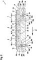
- Fig. 2 is a longitudinal section of a first embodiment of the electrical equipment 2.
- the cooling device 15 comprises a first main wall 16, which has a first side 17 carrying the semiconductor switching elements 10, 11 and a second side 18 being opposite thereto, and a second main wall 19 being opposite to the first main wall 16.
- a cooling channel 20 is defined by the second side 18 of the first main wall 16 and the second main wall 19 and allows a coolant to flow along the main walls 16, 19 in a main flow direction 21.
- the cooling device 15 comprises a first side wall 22 and a second side wall 23 that extend perpendicularly from the first main wall 16 so that the main flow direction 21 is directed form the first side wall 22 to the second side wall 23.
- the cooling device 15 comprises two connection channels, which lead into the cooling channel 20 through the second main wall 19.
- the first connection channel is an inlet channel 24 for supplying the coolant to the cooling channel 20 and the second connection channel is an outlet channel 25 for draining the coolant out of the cooling channel 20.
- a first guiding device 26 of the cooling device 15 is arranged within the inlet channel 24 .
- the first guiding device 26 is configured to direct the coolant towards a first edge 27a formed by the first main wall 16 and the first side wall 22.
- the first guiding device 26 comprises a flap 26a being bent into the direction of the first edge 27a.
- a second guiding device 29 of the cooling device 15 is arranged within the outlet channel 25 .
- the second guiding device 29 is configured to direct the coolant towards a second edge 27b formed by the first main wall 16 and the second side wall 23.
- the second guiding device 29 comprises a flap 29a being bent towards the second main wall, therein narrowing the outlet channel 25 on a side of the outlet channel 25 being opposite to the second side wall 23.
- the guiding devices 26, 29 each comprise a body 26b, 29b, from which the respective flap 26a, 29a is bent off.
- Each body 26b, 26c partially corresponds to a shape of the inlet channel 24 or the outlet channel 25, respectively.
- the body 26b of the first guiding device 26 has an attachment section 26c that is attached to the first side wall 22 and an attachment section 26d that is attached to a wall 30a of the inlet channel 24 being opposite to the first side wall 22.
- the body 29b of the second guiding device 29 has an attachment section 29c that is attached to the second side wall 23 and an attachment section 29d that is attached to a wall 30b of the outlet channel 25 being opposite to the second side wall 23.
- Each body 26b, 29b further comprises a bridge section 26e, 29e that connects the attachment sections 26c, 26d or the attachment sections 29c, 29d, respectively.
- a splitting section 26f of the body 26b extends from the bridge section 26e along the inlet channel 24 and splits the inlet channel 24 partially into two parallel parts.
- the flap 26a extends from the splitting section 26f.
- a splitting section 29f of the body 29b extends from the bridge section 29e along the outlet channel 25 and splits the inlet channel 25 partially into two parallel parts.
- the flap 29a extends from the splitting section 29f.
- the position of the body 26b of the first guiding device 26 influences the fraction of fluid which is redirected into the deadwater/recirculation region of the prior art. Said position can therefore be used as a design parameter for optimizing the heat exchange.
- the cooling channel 20 is formed by a cavity 31 within a housing element 32 of the cooling device 15.
- the first main wall 16 is formed by a base plate 33 that closes the cavity 31.
- the second main wall 19 is formed by a bottom 35 of the cavity 31.
- the housing element 32 and the base plate 33 are made of aluminum, whereas the guiding devices 26, 29 are made of a sheet material, e.g. plastics or metal.
- the inlet channel 24 and the outlet channel 25 are formed by through-holes that are aligned perpendicularly to the second main wall 19. Therein, the through-holes and the cavity 31 are formed by casting the housing element 32. Within restrictions of the casting process it is also possible that the inlet channel and the outlet channel 25 enclose an obtuse angle with the second main wall 19. After casting the housing element 32 the guiding devices 24, 29 are placed into the corresponding connection channels and the cavity 31 is closed by the base plate 33
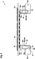
- Fig. 3 is a longitudinal section of a second embodiment of the electrical equipment 2.
- the second embodiment corresponds to the first embodiment unless differences are described in the following. Therein, identical reference signs denote identical or equivalent components.
- the inlet channel 24 is connected to a supply channel 36a.
- the supply channel 36a extends on an end of the inlet channel 24, said end is opposite to a cooling-channel-side end of the inlet channel 24, substantially in parallel to a plane defined by the first main wall 16.
- the outlet channel 25 is connected to a drain channel 36b.
- the drain channel 36b extends on an end of the outlet channel 25, said end is opposite to a cooling-channel-side end of the outlet channel 25, substantially in parallel to the afore-mentioned plane.
- the flap 26a of the first guiding device 26 extends from the wall 30a being opposite to the first side wall 22 towards the edge 27a.
- the flap 29a of the second guiding device 29 extends from the wall 30b being opposite to the second side wall 23 towards the second side wall 23.
- Fig. 4 and Fig. 5 are perspective views of the first guiding device 26 according to the second embodiment.
- the attachment sections 26c, 26d of the body 26b have a plate-like shape.
- the attachment section 26c is attached to the first side wall 22 and the attachment section 26d is attached to the wall 30a (see Fig. 3 ).
- the flap 26a is bent off the attachment section 26d.
- the body 26b has a further attachment section 26g that has the shape of a part of a wall of the inlet channel 24 that connects the first side wall 22 and the wall 30a (see Fig. 3 ).
- Fig. 6 and Fig. 7 are perspective views of the second guiding device 29 according to the second embodiment.
- the attachment sections 29d of the body 29b that is attached to the wall 30b has a plate-like shape.
- Two further attachment sections 29g, 29h extend from the attachment section 29d.
- the attachment section 29g is attached to the second side wall 23 as well as to a wall of the outlet channel 25 that connects the second side wall 23 and the wall 30b.
- the attachment section 29h is attached to second side wall 23 and to the other wall connecting the second side wall 23 and the wall 30b.
- Another attachment section 29i is provided with the body 29b, which is attached to a bottom 37 of the outlet channel 25. Therein, the bottom 37 may be considered as transition section between the outlet channel 25 and the drain channel 36b.
- the flap 29a is provided with two attachment members 38a, 38b that are bent into the direction of the first main wall 16 and attached to the walls connecting the second side wall 23 and the wall 30b.
- pin fins 34 see Fig. 2
- ribbon bonds 39 see Fig. 3
- other heat sink structures are attached the second side 18 first wall 16.
- the guiding devices 24, 29 allow an improved heat transfer from outermost pin fins 34, ribbon bonds 39 or heat sink structures, respectively.
- the attachment members and/or attachment sections of the guiding devices 26, 29 come against the respective wall to be attached.
- the attachment members and/or attachment sections come against the respective walls, the guiding device 26, 29 being force-fitted in the respective connection channel.
Landscapes
- Engineering & Computer Science (AREA)
- Physics & Mathematics (AREA)
- Thermal Sciences (AREA)
- Mechanical Engineering (AREA)
- General Engineering & Computer Science (AREA)
- Cooling Or The Like Of Semiconductors Or Solid State Devices (AREA)
- Inverter Devices (AREA)
Abstract
Description
- The present invention relates to a cooling device for semiconductor switching elements, comprising a first main wall for carrying the semiconductor switching elements, a second main wall being opposite to the first main wall, a cooling channel that is defined by the first main wall and the second main wall and allows a coolant to flow along the main walls in a main flow direction, a first side wall and a second side wall each extending from the first main wall, wherein the main flow direction is directed from one of the side walls to the other side wall, and at least one connection channel, which leads into the cooling channel through the second main wall.
- Besides, the invention relates to a power inverter device, an arrangement with a power inverter device and with an electric machine and to a method for manufacturing a cooling device.
- When operating semiconductor switching elements, exemplarily within a power inverter device that supplies an electric machine of an electric driven vehicle, significant power losses are generated that may cause overtemperature failures of the semiconductor switching elements. It is known to use a cooling device for cooling the semiconductor switching elements that has a cooling channel in order to allow a coolant to flow along the semiconductor switching elements for cooling them. Cooling channels may have two parallel main walls, along which the coolant flows, and connections channels which supply or drain, respectively, the coolant. If the coolant is supplied or drained through one main wall that is opposite to the main wall carrying the semiconductor switching elements, edge regions between the other main wall and a side wall may not be cooled sufficiently.
- Thus, it is an object of the invention to provide an improved possibility for cooling semiconductor switching elements, particularly with respect to applications in electrically driven vehicles.
- According to the invention the above object is solved by a cooling device as initially described, wherein at least one guiding device is arranged within the at least one connection channel and configured to direct the coolant towards an edge formed by the first main wall and one of the side walls.
- The invention aims to avoid recirculations and/or deadwater regions around the edge by guiding the coolant towards the edge, when the coolant changes its flow direction because of a transition between the connection channel and the cooling channel. Therein, it has to be noted that due to restrictions in a manufacturing process of the cooling device, e.g. casting restrictions, an angle between the second main wall and the connection channel cannot always be formed such that the coolant reaches the edge sufficiently. Thereto, the cooling device according to the invention provides the at least one guiding device that resolves recirculations and guides the coolant into such edge regions. Advantageously, the cooling device provides an easily castable cooling channel and has an increased cooling efficiency realized by the cheap guiding device.
- Preferably, a connection channel of the cooling device according to the invention is an inlet channel for supplying the coolant to the cooling channel, wherein a guiding device is arranged within the inlet channel and configured to direct the coolant towards the edge formed by the first main wall and the first side wall. This guiding device may also be regarded as first guiding device. This allows to cool edge regions near the inlet channel. The cooling device may be attached to wall of the inlet channel being opposite to the first side wall.
- Therein, the guiding device may comprise a flap being bent into the direction of the edge.
- Also, the guiding device may comprise a body having at least one attachment section configured to fix said guiding device in the inlet channel. Therein, an attachment section may be configured to come against the first side wall and/or an attachment section may be configured to come against a wall of the inlet channel being opposite to the first side wall and/or an attachment section may be configured to come against a wall connecting the first side wall and the or a wall of the inlet channel being opposite to the first side wall.
- Alternatively or additionally, a connection channel of the cooling device according to the invention is an outlet channel for draining the coolant out of the cooling channel, wherein a guiding device may be arranged within the outlet channel and configured to direct the coolant towards the edge being formed by the first main wall and the second side wall. This allows to cool edge regions near the outlet channel. This guiding device may also be regarded as second guiding device.
- Preferably, the guiding device is configured to narrow the outlet channel on a side of the outlet channel being opposite to the second side wall. Thereby, the coolant can be guided nearer towards the edge by prohibiting to flow directly into the outlet channel on the second side wall.
- Preferably, the guiding device comprises a flap being bent towards the second main wall.
- Alternatively, the guiding device may comprise a flap being bent towards the second side wall. Therein, the guiding device may be attached to a wall of the outlet channel being opposite to the second side wall.
- The guiding device may comprises a body having at least one attachment section configured to fix said guiding device in the outlet channel. Therein, an attachment section may be configured to come against the second side wall and/or an attachment section may be configured to come against a wall of the outlet channel being opposite to the second side wall and/or an attachment section or two attachment sections, wherein the or each attachment section may be configured to come against a wall connecting the second side wall and the wall of the outlet channel being opposite to the second side wall and/or one attachment section may be configured to come against a bottom of the outlet channel.
- The or each attachment section configured to come against the wall connecting the second side wall and the wall of the outlet channel being opposite to the second side wall may further be configured to come against the second side wall.
- According to a specific embodiment, the body of the first guiding device and/or the second guiding device may comprise a bridge section that connects the attachment sections configured to come against the side wall and the wall opposite thereto. The body may further comprise a splitting section that extends from the bridge section along the inlet channel or the outlet channel, respectively, and splits the inlet channel or the outlet channel, respectively, into two parallel parts. Therein, the flap may extend from the splitting section.
- With regard to the flap of the first guiding device and/or the flap of the second guiding device, the flap may comprise an attachment member that is bent off and configured to come against the connection channel.
- The at least one guiding device may be made of a sheet material, e.g. from plastics or metal.
- With respect to the cooling device according to the invention it is preferred that the cooling channel is formed by a cavity within a housing element of the cooling device. Such a cavity can be manufactured with low effort e.g. by casting. The housing element may be made of aluminum for realizing a low weight of the cooling device.
- Preferably, the first main wall is formed by a base plate that closes the cavity. The second main wall may be formed by a bottom of the cavity. The at least one connection channel may be formed by through-holes extending from the cavity through the housing element.
- According to the invention the above object is furthermore solved by an electrical equipment, comprising a plurality of semiconductor switching elements and a cooling device for the semiconductor switching elements according to the invention. For instance, the electrical equipment is a power inverter device.
- According to the invention the above object is furthermore solved by an arrangement comprising an electrical equipment according to the invention, said electrical equipment being a power inverter device, and an electric machine being suitable to drive a vehicle, wherein the power inverter device is configured to supply the electric machine.
- According to the invention the above object is furthermore solved by a method for manufacturing a cooling device for semiconductor switching elements according the invention, comprising steps of: casting the housing element so that the at least one connection channel is formed during casting; and arranging the at least one guiding element into the at least one connection channel. All statements referring to the inventive cooling device, the inventive power converter and the inventive arrangement apply analogously to the inventive method so that the above-mentioned advantages may be achieved by the method as well.
- Further details and advantages of the invention are disclosed in the following, wherein reference is made to the schematic drawings, which show:
- Fig. 1
- a block diagram of an embodiment of an arrangement according to the invention with an embodiment of an electrical equipment according to the invention having an embodiment of the cooling device according to the invention;
- Fig. 2
- a longitudinal section of a first embodiment of the electrical equipment;
- Fig. 3
- a longitudinal section of a second embodiment of the electrical equipment;
- Fig. 4
- a first perspective view of the inlet-side guiding device according to the second embodiment;
- Fig. 5
- a second perspective view of the inlet-side guiding device according to the second embodiment;
- Fig. 6
- a first perspective view of the outlet-side guiding device according to the second embodiment; and
- Fig. 7
- a second perspective view of the outlet-side guiding device according to the second embodiment.
-
Fig. 1 is a block diagram of an embodiment of anarrangement 1 with an embodiment of anelectrical equipment 2 and an electric machine 3. Theelectrical equipment 2 is a power inverter device that is configured to supply the electric machine 3. The electric machine 3 is suitable for driving a vehicle such as a battery electric vehicle or a hybrid electric vehicle. Furthermore,Fig. 1 shows a high-voltage battery 4 connected to a DC link of the power inverter device or to thearrangement 1, respectively. - The power inverter device comprises a
DC link capacitor 5, and a semiconductorswitching element module 6 having a first semiconductorswitching element arrangement 7, a second semiconductor switchingelement arrangement 8 and a third semiconductor switchingelement arrangement 9. Each semiconductorswitching element arrangement switching element arrangement semiconductor switching elements 10, 11. Eachsemiconductor switching element 10, 11 has a transistor structure 12 and anantiparallel diode structure 13. The transistor structure 12 and thediode structure 13 may be formed by one or multiple Power-MOSFETs or by one or multiple connections of an IGBT and a diode. - Furthermore, the power inverter device comprises a control unit 14 being configured to control the semiconductor
switching element module 6 or the semiconductorswitching element arrangements cooling device 15 for cooling thesemiconductor switching elements 10, 11. -
Fig. 2 is a longitudinal section of a first embodiment of theelectrical equipment 2. - The
cooling device 15 comprises a firstmain wall 16, which has afirst side 17 carrying thesemiconductor switching elements 10, 11 and asecond side 18 being opposite thereto, and a secondmain wall 19 being opposite to the firstmain wall 16. A coolingchannel 20 is defined by thesecond side 18 of the firstmain wall 16 and the secondmain wall 19 and allows a coolant to flow along themain walls main flow direction 21. Furthermore, thecooling device 15 comprises afirst side wall 22 and asecond side wall 23 that extend perpendicularly from the firstmain wall 16 so that themain flow direction 21 is directed form thefirst side wall 22 to thesecond side wall 23. - Besides, the
cooling device 15 comprises two connection channels, which lead into the coolingchannel 20 through the secondmain wall 19. The first connection channel is aninlet channel 24 for supplying the coolant to the coolingchannel 20 and the second connection channel is anoutlet channel 25 for draining the coolant out of the coolingchannel 20. - Within the inlet channel 24 a
first guiding device 26 of thecooling device 15 is arranged. Thefirst guiding device 26 is configured to direct the coolant towards afirst edge 27a formed by the firstmain wall 16 and thefirst side wall 22. Thefirst guiding device 26 comprises aflap 26a being bent into the direction of thefirst edge 27a. - Besides, within the outlet channel 25 a
second guiding device 29 of thecooling device 15 is arranged. Thesecond guiding device 29 is configured to direct the coolant towards asecond edge 27b formed by the firstmain wall 16 and thesecond side wall 23. Thesecond guiding device 29 comprises aflap 29a being bent towards the second main wall, therein narrowing theoutlet channel 25 on a side of theoutlet channel 25 being opposite to thesecond side wall 23. - As can be seen in
Fig. 2 the guidingdevices body respective flap body inlet channel 24 or theoutlet channel 25, respectively. - The
body 26b of thefirst guiding device 26 has anattachment section 26c that is attached to thefirst side wall 22 and anattachment section 26d that is attached to awall 30a of theinlet channel 24 being opposite to thefirst side wall 22. Correspondingly, thebody 29b of thesecond guiding device 29 has anattachment section 29c that is attached to thesecond side wall 23 and anattachment section 29d that is attached to awall 30b of theoutlet channel 25 being opposite to thesecond side wall 23. - Each
body bridge section attachment sections attachment sections splitting section 26f of thebody 26b extends from thebridge section 26e along theinlet channel 24 and splits theinlet channel 24 partially into two parallel parts. Therein, theflap 26a extends from thesplitting section 26f. Correspondingly, asplitting section 29f of thebody 29b extends from thebridge section 29e along theoutlet channel 25 and splits theinlet channel 25 partially into two parallel parts. Therein, theflap 29a extends from thesplitting section 29f. - Generally, the position of the
body 26b of thefirst guiding device 26 influences the fraction of fluid which is redirected into the deadwater/recirculation region of the prior art. Said position can therefore be used as a design parameter for optimizing the heat exchange. - The cooling
channel 20 is formed by acavity 31 within ahousing element 32 of thecooling device 15. The firstmain wall 16 is formed by abase plate 33 that closes thecavity 31. The secondmain wall 19 is formed by a bottom 35 of thecavity 31. Therein, thehousing element 32 and thebase plate 33 are made of aluminum, whereas the guidingdevices - The
inlet channel 24 and theoutlet channel 25 are formed by through-holes that are aligned perpendicularly to the secondmain wall 19. Therein, the through-holes and thecavity 31 are formed by casting thehousing element 32. Within restrictions of the casting process it is also possible that the inlet channel and theoutlet channel 25 enclose an obtuse angle with the secondmain wall 19. After casting thehousing element 32 the guidingdevices cavity 31 is closed by thebase plate 33 -
Fig. 3 is a longitudinal section of a second embodiment of theelectrical equipment 2. The second embodiment corresponds to the first embodiment unless differences are described in the following. Therein, identical reference signs denote identical or equivalent components. - In the second embodiment the
inlet channel 24 is connected to asupply channel 36a. Thesupply channel 36a extends on an end of theinlet channel 24, said end is opposite to a cooling-channel-side end of theinlet channel 24, substantially in parallel to a plane defined by the firstmain wall 16. Theoutlet channel 25 is connected to adrain channel 36b. Thedrain channel 36b extends on an end of theoutlet channel 25, said end is opposite to a cooling-channel-side end of theoutlet channel 25, substantially in parallel to the afore-mentioned plane. - According to the second embodiment the
flap 26a of thefirst guiding device 26 extends from thewall 30a being opposite to thefirst side wall 22 towards theedge 27a. Theflap 29a of thesecond guiding device 29 extends from thewall 30b being opposite to thesecond side wall 23 towards thesecond side wall 23. -
Fig. 4 and Fig. 5 are perspective views of thefirst guiding device 26 according to the second embodiment. - The
attachment sections body 26b have a plate-like shape. Theattachment section 26c is attached to thefirst side wall 22 and theattachment section 26d is attached to thewall 30a (seeFig. 3 ). Theflap 26a is bent off theattachment section 26d. Thebody 26b has afurther attachment section 26g that has the shape of a part of a wall of theinlet channel 24 that connects thefirst side wall 22 and thewall 30a (seeFig. 3 ). -
Fig. 6 and Fig. 7 are perspective views of thesecond guiding device 29 according to the second embodiment. - The
attachment sections 29d of thebody 29b that is attached to thewall 30b has a plate-like shape. Twofurther attachment sections attachment section 29d. Theattachment section 29g is attached to thesecond side wall 23 as well as to a wall of theoutlet channel 25 that connects thesecond side wall 23 and thewall 30b. Theattachment section 29h is attached tosecond side wall 23 and to the other wall connecting thesecond side wall 23 and thewall 30b. Anotherattachment section 29i is provided with thebody 29b, which is attached to a bottom 37 of theoutlet channel 25. Therein, the bottom 37 may be considered as transition section between theoutlet channel 25 and thedrain channel 36b. - The
flap 29a is provided with twoattachment members main wall 16 and attached to the walls connecting thesecond side wall 23 and thewall 30b. - Optionally, with regard to the afore-mentioned embodiments pin fins 34 (see
Fig. 2 ), ribbon bonds 39 (seeFig. 3 ) or other heat sink structures are attached thesecond side 18first wall 16. Thereby, the guidingdevices outermost pin fins 34,ribbon bonds 39 or heat sink structures, respectively. - In the above embodiments, the attachment members and/or attachment sections of the guiding
devices device
Claims (15)
- Cooling device (15) for semiconductor switching elements (10, 11), comprising- a first main wall (16) for carrying the semiconductor switching elements (10, 11),- a second main wall (19) being opposite to the first main wall (16),- a cooling channel (20) that is defined by the first main wall (16) and the second main wall (19) and allows a coolant to flow along the main walls (16, 19) in a main flow direction (21),- a first side wall (22) and a second side wall (23) each extending from the first main wall (16), wherein the main flow direction (21) is directed from one of the side walls (22) to the other side wall (23), and- at least one connection channel, which leads into the cooling channel (20) through the second main wall (19),characterized in that
at least one guiding device (26, 29) is arranged within the at least one connection channel and configured to direct the coolant towards an edge (27a, 27b), formed by the first main wall (16) and one of the side walls (22, 23). - Cooling device according to claim 1, wherein
a connection channel is an inlet channel (24) for supplying the coolant to the cooling channel (20), wherein a guiding device (26) is arranged within the inlet channel (24) and configured to direct the coolant towards the edge (27a) being formed by the first main wall (16) and the first side wall (22). - Cooling device according to claim 2, wherein
the guiding device (26) comprises a flap (26a) being bent into the direction of the edge (27a). - Cooling device according to claim 2 or 3, wherein
the guiding device (26) comprises a body (26b) having at least one attachment section (26c, 26d, 26g) configured to fix said guiding device (26c, 26d, 26g) in the inlet channel (24), wherein- an attachment section (26c) is configured to come against the first side wall (22) and/or- an attachment section (26d) is configured to come against a wall (30a) of the inlet channel (24) being opposite to the first side wall (22) and/or- an attachment section (26g) is configured to come against a wall connecting the first side wall (22) and the or a wall (30a) of the inlet channel (24) being opposite to the first side wall (22). - Cooling device according to any of the preceding claims, wherein
a connection channel is an outlet channel (25) for draining the coolant out of the cooling channel (20), wherein a guiding device (29) is arranged within the outlet channel (25) and configured to direct the coolant towards the edge (27b) being formed by the first main wall (16) and the second side wall (23). - Cooling device according to claim 5, wherein
the guiding device (29) is configured to narrow the outlet channel (25) on a side of the outlet channel (25) being opposite to the second side wall (23). - Cooling device according to claim 5 or 6, wherein
the guiding device (29) comprises a flap (29a) being bent towards the second main wall (19) or towards the second side wall (23). - Cooling device according to any of claims 5 to 7, wherein
the guiding device (29) comprises a body (29b) having at least one attachment section (29c, 29d, 29g, 29h, 29i), wherein- an attachment section (29c) is configured to come against the second side wall (23) and/or- an attachment section (29d) is configured to come against a wall (30b) of the outlet channel (25) being opposite to the second side wall (23) and/or- an attachment section or two attachment sections (29g, 29h), wherein the or each attachment section (29g, 29h) is configured to come against a wall connecting the second side wall (23) and the or a wall (30a) of the outlet channel (25) being opposite to the second side wall (23) and/or- an attachment section (29i) is configured to come against a bottom (37) of the outlet channel (25). - Cooling device according any of the preceding claims, wherein
the at least one guiding device (26, 29) is made of a sheet material. - Cooling device according to any of the preceding claims, wherein
the cooling channel (20) is formed by a cavity (31) within a housing element (32) of the cooling device (15). - Cooling device according to claim 10, wherein- the first main wall (16) is formed by a base plate (33) that closes the cavity (31)and/or
the second main wall (19) is formed by a bottom (35) of the cavity (31). - Cooling device according to claim 10 or 11, wherein
the at least one connection channel is formed by through-holes extending from the cavity (31) though the housing element (32). - Electrical equipment (2), comprising a plurality of semiconductor switching elements (10, 11) and a cooling device (15) for the semiconductor switching elements (10, 11) according to any of the preceding claims.
- Arrangement (1) comprising an electrical equipment (2) according to claim 13, said electrical equipment being a power inverter device, and an electric machine (3) being suitable to drive a vehicle, wherein the power inverter device is configured to supply the electric machine (3).
- Method for manufacturing a cooling device (15) according to any of claims 10 to 12, comprising steps of:- casting the housing element (32) so that the at least one connection channel is formed during casting; and- arranging the at least one guiding element (26, 29) into the at least one connection channel.
Priority Applications (1)
| Application Number | Priority Date | Filing Date | Title |
|---|---|---|---|
| EP19216160.2A EP3836206B1 (en) | 2019-12-13 | 2019-12-13 | Cooling device for semiconductor switching elements, power inverter device, arrangement and manufacturing method |
Applications Claiming Priority (1)
| Application Number | Priority Date | Filing Date | Title |
|---|---|---|---|
| EP19216160.2A EP3836206B1 (en) | 2019-12-13 | 2019-12-13 | Cooling device for semiconductor switching elements, power inverter device, arrangement and manufacturing method |
Publications (2)
| Publication Number | Publication Date |
|---|---|
| EP3836206A1 true EP3836206A1 (en) | 2021-06-16 |
| EP3836206B1 EP3836206B1 (en) | 2025-05-07 |
Family
ID=69061047
Family Applications (1)
| Application Number | Title | Priority Date | Filing Date |
|---|---|---|---|
| EP19216160.2A Active EP3836206B1 (en) | 2019-12-13 | 2019-12-13 | Cooling device for semiconductor switching elements, power inverter device, arrangement and manufacturing method |
Country Status (1)
| Country | Link |
|---|---|
| EP (1) | EP3836206B1 (en) |
Cited By (1)
| Publication number | Priority date | Publication date | Assignee | Title |
|---|---|---|---|---|
| DE102023123710A1 (en) | 2023-09-04 | 2025-03-06 | Schaeffler Technologies AG & Co. KG | POWER MODULE WITH COOLING CHANNEL |
Citations (3)
| Publication number | Priority date | Publication date | Assignee | Title |
|---|---|---|---|---|
| WO2007049807A1 (en) * | 2005-10-28 | 2007-05-03 | Toyota Jidosha Kabushiki Kaisha | Cooling structure of electric device |
| EP2080978A2 (en) * | 2008-01-15 | 2009-07-22 | Kabushiki Kaisha Toyoda Jidoshokki | Liquid-cooled-type cooling device |
| US20150102480A1 (en) * | 2013-10-16 | 2015-04-16 | Fuji Electric Co., Ltd. | Semiconductor device |
-
2019
- 2019-12-13 EP EP19216160.2A patent/EP3836206B1/en active Active
Patent Citations (3)
| Publication number | Priority date | Publication date | Assignee | Title |
|---|---|---|---|---|
| WO2007049807A1 (en) * | 2005-10-28 | 2007-05-03 | Toyota Jidosha Kabushiki Kaisha | Cooling structure of electric device |
| EP2080978A2 (en) * | 2008-01-15 | 2009-07-22 | Kabushiki Kaisha Toyoda Jidoshokki | Liquid-cooled-type cooling device |
| US20150102480A1 (en) * | 2013-10-16 | 2015-04-16 | Fuji Electric Co., Ltd. | Semiconductor device |
Cited By (1)
| Publication number | Priority date | Publication date | Assignee | Title |
|---|---|---|---|---|
| DE102023123710A1 (en) | 2023-09-04 | 2025-03-06 | Schaeffler Technologies AG & Co. KG | POWER MODULE WITH COOLING CHANNEL |
Also Published As
| Publication number | Publication date |
|---|---|
| EP3836206B1 (en) | 2025-05-07 |
Similar Documents
| Publication | Publication Date | Title |
|---|---|---|
| US7742303B2 (en) | Electric power converter | |
| JP5407275B2 (en) | Power converter | |
| US9072197B2 (en) | Cooling apparatus | |
| US7252167B2 (en) | Electrical apparatus, cooling system therefor, and electric vehicle | |
| US20150216089A1 (en) | Cooling structure and heat generating body | |
| JP7655915B2 (en) | Cooling device for semiconductor switching elements, power inverter device, and arrangement comprising a power inverter device and an electric machine | |
| US20160307821A1 (en) | Cooler and cooler fixing method | |
| WO2006103721A1 (en) | Power converter cooling structure | |
| CN113728546A (en) | Power conversion device | |
| EP3836206B1 (en) | Cooling device for semiconductor switching elements, power inverter device, arrangement and manufacturing method | |
| EP3758059A1 (en) | Power inverter device, arrangement and corresponding operating method | |
| JP7164545B2 (en) | Semiconductor equipment, power modules and power supplies | |
| JP6921282B1 (en) | Power converter | |
| US20170084515A1 (en) | Power-Module Device and Power Conversion Device | |
| KR101911618B1 (en) | Power module including heat sink | |
| EP3836205A1 (en) | Cooling device for semiconductor switching elements, power inverter device, arrangement and manufacturing method | |
| CN223391558U (en) | Power conversion equipment | |
| EP3474426B1 (en) | Inverter for an electric machine comprising a cooling channel, electric machine for a vehicle and vehicle | |
| JP7861513B2 (en) | Power converter | |
| EP4312261A1 (en) | Cooling device for semiconductor switching elements, power inverter device and arrangement with a power inverter device and an electric machine | |
| KR102920855B1 (en) | Power module cooling device and power converter equipped with the same | |
| JP7233510B1 (en) | power converter | |
| US12621968B2 (en) | Power electronic arrangement for an electric machine and motor vehicle |
Legal Events
| Date | Code | Title | Description |
|---|---|---|---|
| PUAI | Public reference made under article 153(3) epc to a published international application that has entered the european phase |
Free format text: ORIGINAL CODE: 0009012 |
|
| STAA | Information on the status of an ep patent application or granted ep patent |
Free format text: STATUS: THE APPLICATION HAS BEEN PUBLISHED |
|
| AK | Designated contracting states |
Kind code of ref document: A1 Designated state(s): AL AT BE BG CH CY CZ DE DK EE ES FI FR GB GR HR HU IE IS IT LI LT LU LV MC MK MT NL NO PL PT RO RS SE SI SK SM TR |
|
| STAA | Information on the status of an ep patent application or granted ep patent |
Free format text: STATUS: REQUEST FOR EXAMINATION WAS MADE |
|
| 17P | Request for examination filed |
Effective date: 20211210 |
|
| RBV | Designated contracting states (corrected) |
Designated state(s): AL AT BE BG CH CY CZ DE DK EE ES FI FR GB GR HR HU IE IS IT LI LT LU LV MC MK MT NL NO PL PT RO RS SE SI SK SM TR |
|
| RAP3 | Party data changed (applicant data changed or rights of an application transferred) |
Owner name: VALEO EAUTOMOTIVE GERMANY GMBH |
|
| P01 | Opt-out of the competence of the unified patent court (upc) registered |
Effective date: 20230528 |
|
| GRAP | Despatch of communication of intention to grant a patent |
Free format text: ORIGINAL CODE: EPIDOSNIGR1 |
|
| STAA | Information on the status of an ep patent application or granted ep patent |
Free format text: STATUS: GRANT OF PATENT IS INTENDED |
|
| INTG | Intention to grant announced |
Effective date: 20241209 |
|
| GRAS | Grant fee paid |
Free format text: ORIGINAL CODE: EPIDOSNIGR3 |
|
| GRAA | (expected) grant |
Free format text: ORIGINAL CODE: 0009210 |
|
| STAA | Information on the status of an ep patent application or granted ep patent |
Free format text: STATUS: THE PATENT HAS BEEN GRANTED |
|
| AK | Designated contracting states |
Kind code of ref document: B1 Designated state(s): AL AT BE BG CH CY CZ DE DK EE ES FI FR GB GR HR HU IE IS IT LI LT LU LV MC MK MT NL NO PL PT RO RS SE SI SK SM TR |
|
| REG | Reference to a national code |
Ref country code: GB Ref legal event code: FG4D |
|
| REG | Reference to a national code |
Ref country code: CH Ref legal event code: EP |
|
| REG | Reference to a national code |
Ref country code: DE Ref legal event code: R096 Ref document number: 602019069579 Country of ref document: DE |
|
| REG | Reference to a national code |
Ref country code: IE Ref legal event code: FG4D |
|
| REG | Reference to a national code |
Ref country code: NL Ref legal event code: MP Effective date: 20250507 |
|
| PG25 | Lapsed in a contracting state [announced via postgrant information from national office to epo] |
Ref country code: PT Free format text: LAPSE BECAUSE OF FAILURE TO SUBMIT A TRANSLATION OF THE DESCRIPTION OR TO PAY THE FEE WITHIN THE PRESCRIBED TIME-LIMIT Effective date: 20250908 Ref country code: FI Free format text: LAPSE BECAUSE OF FAILURE TO SUBMIT A TRANSLATION OF THE DESCRIPTION OR TO PAY THE FEE WITHIN THE PRESCRIBED TIME-LIMIT Effective date: 20250507 Ref country code: ES Free format text: LAPSE BECAUSE OF FAILURE TO SUBMIT A TRANSLATION OF THE DESCRIPTION OR TO PAY THE FEE WITHIN THE PRESCRIBED TIME-LIMIT Effective date: 20250507 |
|
| REG | Reference to a national code |
Ref country code: LT Ref legal event code: MG9D |
|
| PG25 | Lapsed in a contracting state [announced via postgrant information from national office to epo] |
Ref country code: GR Free format text: LAPSE BECAUSE OF FAILURE TO SUBMIT A TRANSLATION OF THE DESCRIPTION OR TO PAY THE FEE WITHIN THE PRESCRIBED TIME-LIMIT Effective date: 20250808 Ref country code: NO Free format text: LAPSE BECAUSE OF FAILURE TO SUBMIT A TRANSLATION OF THE DESCRIPTION OR TO PAY THE FEE WITHIN THE PRESCRIBED TIME-LIMIT Effective date: 20250807 |
|
| PG25 | Lapsed in a contracting state [announced via postgrant information from national office to epo] |
Ref country code: NL Free format text: LAPSE BECAUSE OF FAILURE TO SUBMIT A TRANSLATION OF THE DESCRIPTION OR TO PAY THE FEE WITHIN THE PRESCRIBED TIME-LIMIT Effective date: 20250507 Ref country code: PL Free format text: LAPSE BECAUSE OF FAILURE TO SUBMIT A TRANSLATION OF THE DESCRIPTION OR TO PAY THE FEE WITHIN THE PRESCRIBED TIME-LIMIT Effective date: 20250507 |
|
| REG | Reference to a national code |
Ref country code: AT Ref legal event code: MK05 Ref document number: 1793470 Country of ref document: AT Kind code of ref document: T Effective date: 20250507 |
|
| PG25 | Lapsed in a contracting state [announced via postgrant information from national office to epo] |
Ref country code: BG Free format text: LAPSE BECAUSE OF FAILURE TO SUBMIT A TRANSLATION OF THE DESCRIPTION OR TO PAY THE FEE WITHIN THE PRESCRIBED TIME-LIMIT Effective date: 20250507 |
|
| PG25 | Lapsed in a contracting state [announced via postgrant information from national office to epo] |
Ref country code: HR Free format text: LAPSE BECAUSE OF FAILURE TO SUBMIT A TRANSLATION OF THE DESCRIPTION OR TO PAY THE FEE WITHIN THE PRESCRIBED TIME-LIMIT Effective date: 20250507 |
|
| PG25 | Lapsed in a contracting state [announced via postgrant information from national office to epo] |
Ref country code: AT Free format text: LAPSE BECAUSE OF FAILURE TO SUBMIT A TRANSLATION OF THE DESCRIPTION OR TO PAY THE FEE WITHIN THE PRESCRIBED TIME-LIMIT Effective date: 20250507 |
|
| PG25 | Lapsed in a contracting state [announced via postgrant information from national office to epo] |
Ref country code: RS Free format text: LAPSE BECAUSE OF FAILURE TO SUBMIT A TRANSLATION OF THE DESCRIPTION OR TO PAY THE FEE WITHIN THE PRESCRIBED TIME-LIMIT Effective date: 20250807 |
|
| PG25 | Lapsed in a contracting state [announced via postgrant information from national office to epo] |
Ref country code: IS Free format text: LAPSE BECAUSE OF FAILURE TO SUBMIT A TRANSLATION OF THE DESCRIPTION OR TO PAY THE FEE WITHIN THE PRESCRIBED TIME-LIMIT Effective date: 20250907 |
|
| PG25 | Lapsed in a contracting state [announced via postgrant information from national office to epo] |
Ref country code: LV Free format text: LAPSE BECAUSE OF FAILURE TO SUBMIT A TRANSLATION OF THE DESCRIPTION OR TO PAY THE FEE WITHIN THE PRESCRIBED TIME-LIMIT Effective date: 20250507 |
|
| REG | Reference to a national code |
Ref country code: DE Ref legal event code: R079 Ref document number: 602019069579 Country of ref document: DE Free format text: PREVIOUS MAIN CLASS: H01L0023473000 Ipc: H10W0040470000 |
|
| PG25 | Lapsed in a contracting state [announced via postgrant information from national office to epo] |
Ref country code: SM Free format text: LAPSE BECAUSE OF FAILURE TO SUBMIT A TRANSLATION OF THE DESCRIPTION OR TO PAY THE FEE WITHIN THE PRESCRIBED TIME-LIMIT Effective date: 20250507 Ref country code: DK Free format text: LAPSE BECAUSE OF FAILURE TO SUBMIT A TRANSLATION OF THE DESCRIPTION OR TO PAY THE FEE WITHIN THE PRESCRIBED TIME-LIMIT Effective date: 20250507 |
|
| PGFP | Annual fee paid to national office [announced via postgrant information from national office to epo] |
Ref country code: FR Payment date: 20251230 Year of fee payment: 7 |
|
| PG25 | Lapsed in a contracting state [announced via postgrant information from national office to epo] |
Ref country code: CZ Free format text: LAPSE BECAUSE OF FAILURE TO SUBMIT A TRANSLATION OF THE DESCRIPTION OR TO PAY THE FEE WITHIN THE PRESCRIBED TIME-LIMIT Effective date: 20250507 |
|
| PG25 | Lapsed in a contracting state [announced via postgrant information from national office to epo] |
Ref country code: EE Free format text: LAPSE BECAUSE OF FAILURE TO SUBMIT A TRANSLATION OF THE DESCRIPTION OR TO PAY THE FEE WITHIN THE PRESCRIBED TIME-LIMIT Effective date: 20250507 |
|
| PG25 | Lapsed in a contracting state [announced via postgrant information from national office to epo] |
Ref country code: RO Free format text: LAPSE BECAUSE OF FAILURE TO SUBMIT A TRANSLATION OF THE DESCRIPTION OR TO PAY THE FEE WITHIN THE PRESCRIBED TIME-LIMIT Effective date: 20250507 Ref country code: SK Free format text: LAPSE BECAUSE OF FAILURE TO SUBMIT A TRANSLATION OF THE DESCRIPTION OR TO PAY THE FEE WITHIN THE PRESCRIBED TIME-LIMIT Effective date: 20250507 |
|
| PG25 | Lapsed in a contracting state [announced via postgrant information from national office to epo] |
Ref country code: IT Free format text: LAPSE BECAUSE OF FAILURE TO SUBMIT A TRANSLATION OF THE DESCRIPTION OR TO PAY THE FEE WITHIN THE PRESCRIBED TIME-LIMIT Effective date: 20250507 |
|
| REG | Reference to a national code |
Ref country code: DE Ref legal event code: R097 Ref document number: 602019069579 Country of ref document: DE |
|
| PLBE | No opposition filed within time limit |
Free format text: ORIGINAL CODE: 0009261 |
|
| STAA | Information on the status of an ep patent application or granted ep patent |
Free format text: STATUS: NO OPPOSITION FILED WITHIN TIME LIMIT |
|
| REG | Reference to a national code |
Ref country code: CH Ref legal event code: L10 Free format text: ST27 STATUS EVENT CODE: U-0-0-L10-L00 (AS PROVIDED BY THE NATIONAL OFFICE) Effective date: 20260318 |
|
| PGFP | Annual fee paid to national office [announced via postgrant information from national office to epo] |
Ref country code: DE Payment date: 20251231 Year of fee payment: 7 |
|
| 26N | No opposition filed |
Effective date: 20260210 |