EP3836197A1 - Method of forming and isolating a semiconductur device - Google Patents
Method of forming and isolating a semiconductur device Download PDFInfo
- Publication number
- EP3836197A1 EP3836197A1 EP19214527.4A EP19214527A EP3836197A1 EP 3836197 A1 EP3836197 A1 EP 3836197A1 EP 19214527 A EP19214527 A EP 19214527A EP 3836197 A1 EP3836197 A1 EP 3836197A1
- Authority
- EP
- European Patent Office
- Prior art keywords
- stack
- forming
- substacks
- layer
- semiconductor
- Prior art date
- Legal status (The legal status is an assumption and is not a legal conclusion. Google has not performed a legal analysis and makes no representation as to the accuracy of the status listed.)
- Pending
Links
Images




Classifications
-
- H—ELECTRICITY
- H10—SEMICONDUCTOR DEVICES; ELECTRIC SOLID-STATE DEVICES NOT OTHERWISE PROVIDED FOR
- H10D—INORGANIC ELECTRIC SEMICONDUCTOR DEVICES
- H10D84/00—Integrated devices formed in or on semiconductor substrates that comprise only semiconducting layers, e.g. on Si wafers or on GaAs-on-Si wafers
- H10D84/01—Manufacture or treatment
- H10D84/02—Manufacture or treatment characterised by using material-based technologies
- H10D84/03—Manufacture or treatment characterised by using material-based technologies using Group IV technology, e.g. silicon technology or silicon-carbide [SiC] technology
- H10D84/038—Manufacture or treatment characterised by using material-based technologies using Group IV technology, e.g. silicon technology or silicon-carbide [SiC] technology using silicon technology, e.g. SiGe
-
- H—ELECTRICITY
- H10—SEMICONDUCTOR DEVICES; ELECTRIC SOLID-STATE DEVICES NOT OTHERWISE PROVIDED FOR
- H10D—INORGANIC ELECTRIC SEMICONDUCTOR DEVICES
- H10D62/00—Semiconductor bodies, or regions thereof, of devices having potential barriers
- H10D62/10—Shapes, relative sizes or dispositions of the regions of the semiconductor bodies; Shapes of the semiconductor bodies
- H10D62/117—Shapes of semiconductor bodies
- H10D62/118—Nanostructure semiconductor bodies
- H10D62/119—Nanowire, nanosheet or nanotube semiconductor bodies
- H10D62/121—Nanowire, nanosheet or nanotube semiconductor bodies oriented parallel to substrates
-
- H—ELECTRICITY
- H10—SEMICONDUCTOR DEVICES; ELECTRIC SOLID-STATE DEVICES NOT OTHERWISE PROVIDED FOR
- H10D—INORGANIC ELECTRIC SEMICONDUCTOR DEVICES
- H10D30/00—Field-effect transistors [FET]
- H10D30/01—Manufacture or treatment
- H10D30/014—Manufacture or treatment of FETs having zero-dimensional [0D] or one-dimensional [1D] channels, e.g. quantum wire FETs, single-electron transistors [SET] or Coulomb blockade transistors
-
- H—ELECTRICITY
- H10—SEMICONDUCTOR DEVICES; ELECTRIC SOLID-STATE DEVICES NOT OTHERWISE PROVIDED FOR
- H10D—INORGANIC ELECTRIC SEMICONDUCTOR DEVICES
- H10D30/00—Field-effect transistors [FET]
- H10D30/01—Manufacture or treatment
- H10D30/021—Manufacture or treatment of FETs having insulated gates [IGFET]
- H10D30/031—Manufacture or treatment of FETs having insulated gates [IGFET] of thin-film transistors [TFT]
-
- H—ELECTRICITY
- H10—SEMICONDUCTOR DEVICES; ELECTRIC SOLID-STATE DEVICES NOT OTHERWISE PROVIDED FOR
- H10D—INORGANIC ELECTRIC SEMICONDUCTOR DEVICES
- H10D30/00—Field-effect transistors [FET]
- H10D30/01—Manufacture or treatment
- H10D30/021—Manufacture or treatment of FETs having insulated gates [IGFET]
- H10D30/031—Manufacture or treatment of FETs having insulated gates [IGFET] of thin-film transistors [TFT]
- H10D30/0321—Manufacture or treatment of FETs having insulated gates [IGFET] of thin-film transistors [TFT] comprising silicon, e.g. amorphous silicon or polysilicon
- H10D30/0323—Manufacture or treatment of FETs having insulated gates [IGFET] of thin-film transistors [TFT] comprising silicon, e.g. amorphous silicon or polysilicon comprising monocrystalline silicon
-
- H—ELECTRICITY
- H10—SEMICONDUCTOR DEVICES; ELECTRIC SOLID-STATE DEVICES NOT OTHERWISE PROVIDED FOR
- H10D—INORGANIC ELECTRIC SEMICONDUCTOR DEVICES
- H10D30/00—Field-effect transistors [FET]
- H10D30/40—FETs having zero-dimensional [0D], one-dimensional [1D] or two-dimensional [2D] charge carrier gas channels
- H10D30/43—FETs having zero-dimensional [0D], one-dimensional [1D] or two-dimensional [2D] charge carrier gas channels having one-dimensional [1D] charge carrier gas channels, e.g. quantum wire FETs or transistors having 1D quantum-confined channels
-
- H—ELECTRICITY
- H10—SEMICONDUCTOR DEVICES; ELECTRIC SOLID-STATE DEVICES NOT OTHERWISE PROVIDED FOR
- H10D—INORGANIC ELECTRIC SEMICONDUCTOR DEVICES
- H10D30/00—Field-effect transistors [FET]
- H10D30/60—Insulated-gate field-effect transistors [IGFET]
- H10D30/67—Thin-film transistors [TFT]
- H10D30/6729—Thin-film transistors [TFT] characterised by the electrodes
- H10D30/673—Thin-film transistors [TFT] characterised by the electrodes characterised by the shapes, relative sizes or dispositions of the gate electrodes
- H10D30/6735—Thin-film transistors [TFT] characterised by the electrodes characterised by the shapes, relative sizes or dispositions of the gate electrodes having gates fully surrounding the channels, e.g. gate-all-around
-
- H—ELECTRICITY
- H10—SEMICONDUCTOR DEVICES; ELECTRIC SOLID-STATE DEVICES NOT OTHERWISE PROVIDED FOR
- H10D—INORGANIC ELECTRIC SEMICONDUCTOR DEVICES
- H10D30/00—Field-effect transistors [FET]
- H10D30/60—Insulated-gate field-effect transistors [IGFET]
- H10D30/67—Thin-film transistors [TFT]
- H10D30/674—Thin-film transistors [TFT] characterised by the active materials
- H10D30/6741—Group IV materials, e.g. germanium or silicon carbide
-
- H—ELECTRICITY
- H10—SEMICONDUCTOR DEVICES; ELECTRIC SOLID-STATE DEVICES NOT OTHERWISE PROVIDED FOR
- H10D—INORGANIC ELECTRIC SEMICONDUCTOR DEVICES
- H10D30/00—Field-effect transistors [FET]
- H10D30/60—Insulated-gate field-effect transistors [IGFET]
- H10D30/67—Thin-film transistors [TFT]
- H10D30/674—Thin-film transistors [TFT] characterised by the active materials
- H10D30/6741—Group IV materials, e.g. germanium or silicon carbide
- H10D30/6743—Silicon
- H10D30/6744—Monocrystalline silicon
-
- H—ELECTRICITY
- H10—SEMICONDUCTOR DEVICES; ELECTRIC SOLID-STATE DEVICES NOT OTHERWISE PROVIDED FOR
- H10D—INORGANIC ELECTRIC SEMICONDUCTOR DEVICES
- H10D30/00—Field-effect transistors [FET]
- H10D30/60—Insulated-gate field-effect transistors [IGFET]
- H10D30/67—Thin-film transistors [TFT]
- H10D30/6757—Thin-film transistors [TFT] characterised by the structure of the channel, e.g. transverse or longitudinal shape or doping profile
-
- H—ELECTRICITY
- H10—SEMICONDUCTOR DEVICES; ELECTRIC SOLID-STATE DEVICES NOT OTHERWISE PROVIDED FOR
- H10D—INORGANIC ELECTRIC SEMICONDUCTOR DEVICES
- H10D62/00—Semiconductor bodies, or regions thereof, of devices having potential barriers
- H10D62/10—Shapes, relative sizes or dispositions of the regions of the semiconductor bodies; Shapes of the semiconductor bodies
- H10D62/113—Isolations within a component, i.e. internal isolations
- H10D62/115—Dielectric isolations, e.g. air gaps
- H10D62/116—Dielectric isolations, e.g. air gaps adjoining the input or output regions of field-effect devices, e.g. adjoining source or drain regions
-
- H—ELECTRICITY
- H10—SEMICONDUCTOR DEVICES; ELECTRIC SOLID-STATE DEVICES NOT OTHERWISE PROVIDED FOR
- H10D—INORGANIC ELECTRIC SEMICONDUCTOR DEVICES
- H10D62/00—Semiconductor bodies, or regions thereof, of devices having potential barriers
- H10D62/10—Shapes, relative sizes or dispositions of the regions of the semiconductor bodies; Shapes of the semiconductor bodies
- H10D62/117—Shapes of semiconductor bodies
- H10D62/118—Nanostructure semiconductor bodies
-
- H—ELECTRICITY
- H10—SEMICONDUCTOR DEVICES; ELECTRIC SOLID-STATE DEVICES NOT OTHERWISE PROVIDED FOR
- H10D—INORGANIC ELECTRIC SEMICONDUCTOR DEVICES
- H10D84/00—Integrated devices formed in or on semiconductor substrates that comprise only semiconducting layers, e.g. on Si wafers or on GaAs-on-Si wafers
- H10D84/01—Manufacture or treatment
- H10D84/0123—Integrating together multiple components covered by H10D12/00 or H10D30/00, e.g. integrating multiple IGBTs
- H10D84/0126—Integrating together multiple components covered by H10D12/00 or H10D30/00, e.g. integrating multiple IGBTs the components including insulated gates, e.g. IGFETs
- H10D84/0165—Integrating together multiple components covered by H10D12/00 or H10D30/00, e.g. integrating multiple IGBTs the components including insulated gates, e.g. IGFETs the components including complementary IGFETs, e.g. CMOS devices
- H10D84/0172—Manufacturing their gate conductors
-
- H—ELECTRICITY
- H10—SEMICONDUCTOR DEVICES; ELECTRIC SOLID-STATE DEVICES NOT OTHERWISE PROVIDED FOR
- H10D—INORGANIC ELECTRIC SEMICONDUCTOR DEVICES
- H10D84/00—Integrated devices formed in or on semiconductor substrates that comprise only semiconducting layers, e.g. on Si wafers or on GaAs-on-Si wafers
- H10D84/01—Manufacture or treatment
- H10D84/0123—Integrating together multiple components covered by H10D12/00 or H10D30/00, e.g. integrating multiple IGBTs
- H10D84/0126—Integrating together multiple components covered by H10D12/00 or H10D30/00, e.g. integrating multiple IGBTs the components including insulated gates, e.g. IGFETs
- H10D84/0165—Integrating together multiple components covered by H10D12/00 or H10D30/00, e.g. integrating multiple IGBTs the components including insulated gates, e.g. IGFETs the components including complementary IGFETs, e.g. CMOS devices
- H10D84/0188—Manufacturing their isolation regions
-
- H—ELECTRICITY
- H10—SEMICONDUCTOR DEVICES; ELECTRIC SOLID-STATE DEVICES NOT OTHERWISE PROVIDED FOR
- H10P—GENERIC PROCESSES OR APPARATUS FOR THE MANUFACTURE OR TREATMENT OF DEVICES COVERED BY CLASS H10
- H10P90/00—Preparation of wafers not covered by a single main group of this subclass, e.g. wafer reinforcement
- H10P90/19—Preparing inhomogeneous wafers
- H10P90/1904—Preparing vertically inhomogeneous wafers
- H10P90/1906—Preparing SOI wafers
-
- H—ELECTRICITY
- H10—SEMICONDUCTOR DEVICES; ELECTRIC SOLID-STATE DEVICES NOT OTHERWISE PROVIDED FOR
- H10W—GENERIC PACKAGES, INTERCONNECTIONS, CONNECTORS OR OTHER CONSTRUCTIONAL DETAILS OF DEVICES COVERED BY CLASS H10
- H10W10/00—Isolation regions in semiconductor bodies between components of integrated devices
- H10W10/01—Manufacture or treatment
- H10W10/011—Manufacture or treatment of isolation regions comprising dielectric materials
- H10W10/014—Manufacture or treatment of isolation regions comprising dielectric materials using trench refilling with dielectric materials, e.g. shallow trench isolations
-
- H—ELECTRICITY
- H10—SEMICONDUCTOR DEVICES; ELECTRIC SOLID-STATE DEVICES NOT OTHERWISE PROVIDED FOR
- H10W—GENERIC PACKAGES, INTERCONNECTIONS, CONNECTORS OR OTHER CONSTRUCTIONAL DETAILS OF DEVICES COVERED BY CLASS H10
- H10W10/00—Isolation regions in semiconductor bodies between components of integrated devices
- H10W10/01—Manufacture or treatment
- H10W10/061—Manufacture or treatment using SOI processes together with lateral isolation, e.g. combinations of SOI and shallow trench isolations
-
- H—ELECTRICITY
- H10—SEMICONDUCTOR DEVICES; ELECTRIC SOLID-STATE DEVICES NOT OTHERWISE PROVIDED FOR
- H10W—GENERIC PACKAGES, INTERCONNECTIONS, CONNECTORS OR OTHER CONSTRUCTIONAL DETAILS OF DEVICES COVERED BY CLASS H10
- H10W10/00—Isolation regions in semiconductor bodies between components of integrated devices
- H10W10/10—Isolation regions comprising dielectric materials
- H10W10/17—Isolation regions comprising dielectric materials formed using trench refilling with dielectric materials, e.g. shallow trench isolations
-
- H—ELECTRICITY
- H10—SEMICONDUCTOR DEVICES; ELECTRIC SOLID-STATE DEVICES NOT OTHERWISE PROVIDED FOR
- H10W—GENERIC PACKAGES, INTERCONNECTIONS, CONNECTORS OR OTHER CONSTRUCTIONAL DETAILS OF DEVICES COVERED BY CLASS H10
- H10W10/00—Isolation regions in semiconductor bodies between components of integrated devices
- H10W10/10—Isolation regions comprising dielectric materials
- H10W10/181—Semiconductor-on-insulator [SOI] isolation regions, e.g. buried oxide regions of SOI wafers
-
- B—PERFORMING OPERATIONS; TRANSPORTING
- B82—NANOTECHNOLOGY
- B82Y—SPECIFIC USES OR APPLICATIONS OF NANOSTRUCTURES; MEASUREMENT OR ANALYSIS OF NANOSTRUCTURES; MANUFACTURE OR TREATMENT OF NANOSTRUCTURES
- B82Y10/00—Nanotechnology for information processing, storage or transmission, e.g. quantum computing or single electron logic
Definitions
- the present inventive concept relates to of field of semiconductor devices.
- More particularly it relates to a method of forming and isolating a semiconductor device comprising horizontally stacked nanosheets .
- Horizontal channel field effect transistor (FET) devices include the finFET, which has a gate straddling a channel portion of a fin-shaped semiconductor structure, and the horizontal nanowire- or nanosheet-FET (horizontal NWFET or NSFET), which has a gate at least partly enclosing a channel portion of a horizontally oriented nanowire- or nanosheet-shaped semiconductor structure.
- FET Horizontal channel field effect transistor
- a method of forming a semiconducting device comprising the steps of
- the term vertical denotes a direction being parallel to a vertical geometrical axis extending perpendicular to the substrate.
- the terms “above”, “below”, “upper”, “top”, “lower” “bottom” are thus used to refer to relative positions along the vertical axis, and does hence not imply an absolute orientation of the substrate or device.
- the term lateral or horizontal refers to the direction perpendicular to the vertical direction, i.e. to the direction parallel to the substrate surface.
- the first aspect of the invention is based on the insight that the isolation between individual substacks of nanosheets, i.e. forming a dielectric "wall" between substacks of nanosheets, can be performed simultaneously as providing the bottom isolation.
- both bottom and wall isolation may be filled with the same dielectric material.
- the bottom isolation i.e. the isolation filling the bottom space, separates the substacks of nanosheets from the substrate.
- the substrate surface may be the surface of a semiconductor material, such as a single crystalline, polycrystalline or amorphous semiconductor material.
- the substrate may be single crystalline silicon.
- the stack of horizontally stacked nanosheets may be used to form horizontal channel FET devices, i.e. devices comprising a semiconductor structure comprising a first and a second source/drain portion and a channel portion located intermediate and extending horizontally between the first and second source/drain portions, and further comprising a gate structure extending horizontally along the channel portion.
- horizontal channel FET devices i.e. devices comprising a semiconductor structure comprising a first and a second source/drain portion and a channel portion located intermediate and extending horizontally between the first and second source/drain portions, and further comprising a gate structure extending horizontally along the channel portion.
- the first and second source/drain portions and the channel portion may intersect a common horizontal plane.
- the channel portion is adapted to (in use of the device) conduct a horizontally oriented flow of charge carriers between the source/drains.
- the semiconductor material sheets of the stack formed in step a) may thus be arranged to be used as channels in a formed horizontal channel FET device.
- the bottom semiconductor nanosheet may be arranged on the substrate surface. However, there may be intermediate layers other than horizontally stacked nanosheets between the substrate surface and the bottom semiconductor nanosheet.
- the bottom semiconductor nanosheet may comprise silicon germanium (SiGe).
- the other semiconductor nanosheets of the stack may be of a material such that the bottom semiconductor nanosheet can be selectively removed from the other sheets during step c).
- the bottom semiconductor nanosheet comprises SiGe having a Ge content of over 50%, i.e. Si 1-x Ge x , in which x>0.5.
- the bottom semiconductor nanosheet may be a Si 0.35 Ge 0.65 nanosheet.
- the other semiconductor nanosheets of the stack comprises SiGe sheets having a Ge content of below 40%.
- Si 1-x Ge x nanosheets in which X>0.5, may be selectively removed from other Si 1-x Ge x nanosheets, in which X ⁇ 0.4 during step c) of the method of the first aspect.
- these materials allow of selectively removing the bottom semiconductor nanosheet after forming the trench, thereby allowing for simultaneous fill of the same dielectric material in the trench and in the bottom space extending under the substacks formed when forming the trench.
- the formation of the trench in step b) may be a straight etch through the stack, e.g. using anisotropic etching, i.e. orientation dependent etching, of an exposed upper lateral surface area of the stack.
- the stack provided in step a) may thus be in the form of fins that are cut into two individual substacks by the trench in step b).
- the stack formed in step a) comprises an upper insulator layer above the semiconductor material sheets.
- Such an upper insulator layer may originate from the patterning of the stack, i.e. from the patterning of the fins.
- the upper insulator layer may be a hardener.
- the upper insulator layer may comprise Si 3 N 4 .
- the upper insulator layer may thus be a hardmask, e.g. used as a CMP stopping layer.
- the stack formed in step a) may further comprise a top oxide layer.
- a top oxide layer may originate from the formation of the horizontally stacked nanosheets.
- the top oxide layer may be hardmask during a lithographic patterning of the stacks on the substrate surface.
- the top oxide layer may comprise or consist of SiO 2 .
- the method may comprise the deposition of an STI (shallow trench isolation) oxide such that the semiconductor nanosheets are attached to this STI oxide during the removal of the bottom semiconductor nanosheet in step c).
- an STI oxide may thus be deposited before step c).
- the STI oxide may for example be silicon dioxide.
- step a) further comprises lining said stack with an insulator material and depositing an STI oxide conformally to the lined sidewalls of the stack, such that said stack is held together by said STI oxide during step c).
- the lining of the insulator material may be performed using atomic layer deposition (ALD).
- the lining may thus comprise a deposition of an insulator material on the sidewalls and on top of the stack, such as on top of the top oxide layer.
- the insulator material used for lining may for example be the same as the upper insulator layer.
- the insulator material may be Si 3 N 4 . Lining the stack with an insulator layer may decrease the risk of or prevent oxidation.
- the insulator liner may prevent oxidation on SiGe, e.g. during FCVD oxide annealing.
- Depositing of the STI oxide may be performed using chemical vapor deposition (CVD), such as flowable chemical vapor deposition (FCVD).
- CVD chemical vapor deposition
- FCVD flowable chemical vapor deposition
- the semiconductor structure may be planarized, i.e. the height may be reduced.
- the planarization may remove the top oxide layer.
- Forming the trench in step b) may performed using different approaches.
- step b) comprises the steps of
- forming the trench of step b) may include lithography and etching.
- the planarizing in step b11) may be performed using chemical mechanical polishing (CMP).
- CMP chemical mechanical polishing
- Step b12) may include forming a hardmask on the planarized structure and thereafter depositing a first sacrificial layer such as a spin-on-carbon (SOC) layer, and a second sacrificial layer, such as a spin-on-glass (SOG) layer. Thereafter a photoresist layer may be formed and patterned, using a pattern of irradiation as known in the art.
- the photoresist layer may comprise a hardmask.
- the vertical opening of step b) may include etching processes, such as a straight etch process through vertically down through the stack and the bottom semiconductor nanosheet at the position of the opening formed after lithography.
- step b) comprises
- the trench may be formed without using lithography.
- the trench formed in the stack is "self-aligned", meaning that also the subsequently formed dielectric wall between the substacks may be self-aligned.
- the planarizing of step b21) may for example be performed using chemical mechanical polishing (CMP).
- CMP chemical mechanical polishing
- the removal of the upper insulator layer in step b22) may be performed using an acid, such as phosphoric acid (H 3 PO 4 ).
- an acid such as phosphoric acid (H 3 PO 4 ).
- the upper insulator layer may be removed early in the process, i.e. before formation of the trench.
- the deposited STI thus forms vertically extending portions extending over the stack
- the vertically extending portions may extend all around the stack, thereby forming a continuous vertically extending portion around the stack.
- the vertically extending portions may also be formed so that they extend on two opposite sides of the stack, as seen in a cross-section through the stack.
- the height above the stack of the vertically extending portions may be lower than the horizontal width of the stack.
- deposition processes that can be used in depositing the spacer material include, for example, CVD, PVD, PECVD or atomic layer deposition (ALD). Plasma Enhanced Atomic Layer Deposition (PEALD).
- the spacer material may for example be an oxide, such as SiO 2 .
- the spacer material is deposited at vertically extending sidewalls such that a small lateral gap is left between the vertical extending structures. This gap is positioned vertically over the stack. As an example, the gap may be positioned substantially in the middle of the stack, such that the subsequent etching in the gap in step b24) divides the stack into two sub stacks of substantially the same size.
- the depositing of spacer material of step b23) may comprise a first deposition of spacer material, followed by a spacer etch.
- the spacer etch may include an anisotropic etch to remove spacer material that has been deposited on horizontal surfaces.
- etching that may be used for etching the deposited spacer material is reactive-ion etching RIE.
- the upper insulator layer may be trimmed in order to reduce the width of this layer before STI deposition.
- the lateral distance of the subsequently conformally deposited STI oxide will be shorter over the stack, meaning that after removal of the upper insulator layer in step b22), the vertically extending portion will be arranged closer to each other compared to if no trimming is performed.
- step a) may further comprise trimming the sidewalls of said upper insulator layer such that the upper insulator layer has a width that is smaller than the width of the semiconductor material sheets of the stack, said trimming being performed before lining said stack with an insulator material.
- Such a step of trimming may allow for a higher aspect ratio of the subsequently formed dielectric wall between the substacks, i.e. the width of the dielectric wall may be reduced.
- the simultaneous filling of the bottom space and the trench in step d) is performed using the same dielectric material.
- the dielectric material may comprise a silicon nitride (SiN) based material, a silicon carbon oxide (SiCO)-based material, silicon carbonitride (SiOCN, SiON), or silicon carbide (SiC).
- the dielectric material of step d) may be selected from the group consisting of comprises Si 3 N 4 , SiCO and SiO 2 .
- the dielectric material may be Si 3 N 4 .
- the method further comprises a step e) of planarizing the isolated substacks of step d).
- Such a planarization may be performed using chemical mechanical polishing (CMP).
- CMP chemical mechanical polishing
- the method further comprises forming gates around the substacks.
- the method may first comprise removing sacrificial layers that are present in the substacks between the semiconductor nanosheets.
- the gates may be formed such that they at least partly wrap around the semiconductor nanosheets of the substacks.
- gate structures may be formed such that they fully wrap around the released semiconductor nanosheets of the substacks, i.e. the released cannel portions.
- the distance between semiconductor nanosheets in the substacks may allow for forming a gate-all-around (GAA) structure, which may reduce the operating voltage of the FET device.
- GAA gate-all-around
- the gate around a first substack may be a p-gate and the gate around a second substack may be an n-gate.
- Forming the gates may thus comprise forming a p-type effective work function metal, WFM, on the first and second substacks. Forming the gates may further comprise selectively removing the p-type WFM from the second substack. Then, an n-type WFM may be formed on the second substack, which may be followed by forming a first gate electrode in contact with the first substack and a second gate electrode in contact with the second substack.
- WFM effective work function metal
- the method of the present disclosure provides for closer proximity of n-type and p-type semiconductor devices.
- Figs. 1a and 1b shows the general approach of the present disclosure for simultaneous wall formation and bottom isolation of a semiconductor device 1 .
- the semiconductor device comprises a stack 2 of horizontally stacked nanosheets on a substrate surface.
- the method comprises a step of forming a trench 3 in the stack, thereby dividing the stack 2 into two substacks 21, 22, and also selectively removing a bottom sheet to create a bottom space 4.
- the stack may be attached to e.g. an STI oxide 8.
- the trench 3 and the bottom space 4 may be simultaneously filled with the same dielectric material 13. Consequently, the formation of the wall between substacks and the bottom isolation may be performed while using STI oxide for holding the fins of the stack 2, instead of performing the isolation during e.g. subsequent gate patterning.
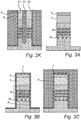
- Figs. 2a-2k illustrate a method according to a first embodiment for forming a semiconductor device according to the present disclosure.
- the method comprises a first step a) of forming a stack 2 of horizontally stacked nanosheets on a substrate surface 20 of Si.
- the stack 2 comprises semiconductor material sheets 2b and a bottom semiconductor nanosheet 2a.
- the bottom semiconductor nanosheet 2a is a Si 0.35 Ge 0.65 sheet
- the other semiconductor nanosheets 2b of the stack 2 comprises SiGe sheets having a Ge content of below 40%.
- the stack of semiconductor material sheets formed in step a) may comprise alternating SiGe sheets and sheets of another material.
- the channel material of the stack 2b may be Si, and the sacrificial material may be SiGe.
- Such a combination of materials may allow for selective removal of the sacrificial material while leaving the channel material.
- the channel material of the stack 2b may be silicon germanium SiGe and the sacrificial material may be silicon Si.
- the channel material of the stack 2b may be silicon germanium with a first concentration of germanium Si 1-x Ge x and the sacrificial material may be silicon germanium with a second concentration of germanium, different from the first concentration Si 1-y Ge y .
- Another combination may be using germanium (Ge) as the channel material, and silicon germanium (SiGe) as the sacrificial material.
- some embodiments may comprise a combination of channel/sacrificial materials wherein one material is from group (or family) III in the periodic table, and the other material is from group (or family) V in the periodic table.
- the channel material may be from group III, also known as the boron group, which comprises boron (B), aluminium (Al), gallium (Ga) and indium (In).
- the sacrificial material may be from group V, also known as the nitrogen group or pnictogens, which comprises nitrogen (N), phosphor (P), arsenic (As) and antimony (Sb).
- the channel material may be selected from group V and the sacrificial material selected from group III.
- the stack 2 formed in step a) comprises an upper insulator layer 5 above said semiconductor material sheets 2b.
- This upper insulator layer 5 may for example be a Si 3 N 4 layer, and may originate from the formation and patterning of the stack 2 on the substrate 20.
- a top oxide layer 6 has also been formed as the uppermost layer, which also may originate from the formation of the stack 2, e.g. during lithography.
- the top oxide layer 6 is in this example a SiO 2 layer. Both the upper insulator layer 5 and the top oxide layer 6.
- step a) further comprises lining the stack 2 with an insulator material 7. This may for example be performed using ALD.
- the stack 2 may for example be lined with Si 3 N 4 .
- the lining of the stack 2 may prevent oxidation.
- step a) may further comprise the deposition of an STI oxide 8 and subsequent planarization using e.g. CMP.
- the STI oxide 8 is deposited to the lined sidewalls 2c of the stack 2 such that the stack 2 may be held together by the STI oxide 8 during a simultaneous bottom isolation and wall formation of step c).
- the formed structure is planarized. In this example, it is planarized such that the upper insulator layer 5 is the uppermost layer of the stack 2.
- a patterned photoresist layer 9 is then formed atop of the stack such that an opening 10 in the photoresist layer 9 is positioned vertically over the stack 2.
- the width of the opening 10 determines the width of the trench that is subsequently formed for dividing the stack 2 into the two substacks.
- the step of forming the opening 10 comprises depositing a hardmask layer 14, such as SiO 2 , on top of the stack 2, and thereafter depositing a patterning stack which is used for patterning.
- the patterning stack may comprise a SoC layer 15, a SoG layer 16 and an upper photoresist 9 over the hardmask 14, which is patterned using any suitable photomask.
- the SoG and the SoC layers are then etched at the position of the opening 10 after removal of the photoresist layer, as illustrated in Fig. 2f .
- the hardmask 14 and the upper insulator layer 5 are etched using a suitable hard-mask open (HMO), as illustrated in Fig. 2g , before etching the trench 3 that divides the stack 2 into two substacks 21, 22, as illustrated in Fig. 2h .
- HMO hard-mask open
- the etch through the stacks may be performed using any suitable anisotropic (top-down) etch, and thus divides the stack 2 into two substacks 21, 22.
- step b) comprises the steps of
- the bottom semiconductor nanosheet 2a is selectively removed from the stack 2 in a step c) using e.g. etching based on an ammonia hydroxide-hydrogen peroxide-water mixture (APM). This is illustrated in Fig. 2i .
- APM ammonia hydroxide-hydrogen peroxide-water mixture
- Fig. 2i After removal of the bottom layer 2a, a bottom space 4 is formed under the stack 2, which extends under both of the substacks 21, 22.
- the bottom space 4 and the trench 3 are simultaneously filled in a step d) with the same dielectric material 13 to provide a bottom isolation 4a and formation of a dielectric wall 3a between said substacks 21,22.
- the bottom isolation 4a is thus at the filled bottom space 4 and the dielectric wall 3a is at the position of the previous trench 3.
- the dielectric material 13 that is deposited to form the bottom isolation 4a and the wall 3a may be selected from the group consisting of comprises Si 3 N 4 , SiCO and SiO 2 .
- the deposited dielectric material 13 may then be planarized, as illustrated in Fig. 2k .
- both substacks 21,22 may be planarized such that the upper dielectric material 5 is the uppermost layer of the stack 2.
- Figs. 3a-3k illustrate an embodiment with "self-aligned" wall formation.
- an STI oxide 8 may be deposited after lining the stack with an oxide 7, as discussed in relation to Figs. 2b and 2c above.
- the upper dielectric material 5, such as Si 3 N 4 may be removed using e.g. phosphoric acid (H 3 PO 4 ), as seen in Fig. 3e . In this way, vertically extending sidewalls 8a of the STI oxide 8 are formed around the remaining stack 2.
- spacer material 11 is conformally deposited over the stack 2 and the vertically extending sidewalls, as illustrated in Fig. 3f .
- the spacer material 11 is deposited using e.g. Plasma Enhanced Atomic Layer Deposition (PEALD) to an extend such that a horizontal gap 12 is formed between the sidewalls 8a.
- PEALD Plasma Enhanced Atomic Layer Deposition
- This gap 12 is arranged vertically above the stack 2 and thus defines the position of the trench 3 that is subsequently formed through the stack.
- the deposited spacer material 11 may then be etched-back, as seen in Fig. 3g , and a trench may be formed by etching the stack 2 at the position of the gap 12 formed between the deposited spacer material at the sidewalls 8a of the STI oxide 8, as seen in Fig. 3h .
- step b) comprises
- the bottom layer 8a may be selectively removed and the trench and the bottom space 4 be filled with the same dielectric material as discussed in relation to Figs. 2i and 2j above.
- the formed structure may be further planarized, as illustrated in Fig. 3k .
- the upper insulator layer may be trimmed before depositing of the STI oxide.
- Figs. 4a-4l shows a similar method for forming the trench and the isolation as discussed in relation to Figs. 3a-k above, but with an additional step of trimming the upper insulator layer 5, such as an upper Si 3 N 4 , layer, as illustrated in Fig. 4b , before lining the stack with a Si 3 N 4 liner in Fig. 4c .
- the trimming of the upper insulator layer may be performed using liquid phase or gas phase isotropic etch, such as a dry gas chemical reaction with e.g. HF and NH 3 .
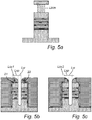
- the trimming operation may be used if the stack is wide, i.e. has a larger extension in the horizontal direction. With a wide stack and no trimming, the gap 12 formed after depositing spacer material at the sidewalls would be larger if depositing the same amount of spacer material. Thus, with no trimming, the trench 3 and subsequent wall separating the two substacks would be wider. Consequently, using a trimming operation of the upper insulator layer 5, a thinner gap 12 and trench 3 may be formed. This is further illustrated in Figs. 5a-c .
- the width of a substack 21, 22 is the width of the STI oxide over a substack (L ox ) + the width of the deposited spacer (L sp ).
- L ox may be adjusted by the trimming operation, i.e. the more the upper insulator layer is trimmed, illustrated by L trim in Fig. 5a , the larger L ox becomes after STI deposition.
- a thin stack is illustrated in Fig. 5b and a wider stack is illustrated in Fig. 5c .
- a different trimming operation can be performed to increase L trim and thus also L ox2 .
- the width of the STI oxide over a substack L ox2 of the wider stack becomes larger than the width of the STI oxide over a substack L ox1 of the thinner stack, as illustrated in Figs. 5b and 5c .
- Figs. 4i-l formation of trench 3 ( Fig. 4i ), selective removal of bottom sheet to form bottom space 4 ( Fig. 4j ), simultaneous isolation of trench 3 and bottom space 4 with dielectric material 13 ( Fig. 4k ) and planarization ( Fig. 4l ) may be performed as discussed in relation to the previous embodiments above.
- step a) further comprises trimming the sidewalls 5a of said upper insulator layer 5 such that the upper insulator layer 5) has a width that is smaller than the width of the semiconductor material sheets 2b of the stack 2, said trimming being performed before lining said stack 2 with an insulator material 7.
Landscapes
- Element Separation (AREA)
- Chemical & Material Sciences (AREA)
- Engineering & Computer Science (AREA)
- Crystallography & Structural Chemistry (AREA)
- Nanotechnology (AREA)
Abstract
Description
- The present inventive concept relates to of field of semiconductor devices.
- More particularly it relates to a method of forming and isolating a semiconductor device comprising horizontally stacked nanosheets .
- In the strive to provide even more power- and area-efficient circuit designs, new transistor devices are being developed.
- Horizontal channel field effect transistor (FET) devices include the finFET, which has a gate straddling a channel portion of a fin-shaped semiconductor structure, and the horizontal nanowire- or nanosheet-FET (horizontal NWFET or NSFET), which has a gate at least partly enclosing a channel portion of a horizontally oriented nanowire- or nanosheet-shaped semiconductor structure.
- Efficient process flows dedicated to fabrication of horizontal channel FET devices have been developed. However, individual horizontal channel field effect transistors need to be positioned close to each other to have area-efficient design, and there may thus be a challenge to efficiently isolate adjacent transistors from each other and to form a bottom isolation. Thus, there is a need in the art for improved methods of forming and isolating semiconductor devices.
- It is an object of the invention to at least partly overcome one or more limitations of the prior art. In particular, it is an object to provide a method allowing for an efficient isolation of semiconductor devices formed on the same substrate.
- As a first aspect of the invention, there is provided a method of forming a semiconducting device, said method comprising the steps of
- a) forming, on a substrate surface, a stack of horizontally stacked nanosheets, said stack comprising semiconductor material sheets and a bottom semiconductor nanosheet:
- b) forming a trench through said stack vertically down through said bottom semiconductor nanosheet; thereby separating the stack into two substacks;
- c) selectively removing said bottom semiconductor nanosheet, thereby forming a bottom space extending under said substacks;
- d) simultaneously filling said bottom space and said trench with the same dielectric material to provide a bottom isolation and formation of a dielectric wall between said substacks.
- As used herein, the term vertical denotes a direction being parallel to a vertical geometrical axis extending perpendicular to the substrate. The terms "above", "below", "upper", "top", "lower" "bottom" are thus used to refer to relative positions along the vertical axis, and does hence not imply an absolute orientation of the substrate or device. In addition, the term lateral or horizontal refers to the direction perpendicular to the vertical direction, i.e. to the direction parallel to the substrate surface.
- The first aspect of the invention is based on the insight that the isolation between individual substacks of nanosheets, i.e. forming a dielectric "wall" between substacks of nanosheets, can be performed simultaneously as providing the bottom isolation. Thus, both bottom and wall isolation may be filled with the same dielectric material.
- The bottom isolation, i.e. the isolation filling the bottom space, separates the substacks of nanosheets from the substrate.
- The substrate surface may be the surface of a semiconductor material, such as a single crystalline, polycrystalline or amorphous semiconductor material. As an example, the substrate may be single crystalline silicon.
- The stack of horizontally stacked nanosheets may be used to form horizontal channel FET devices, i.e. devices comprising a semiconductor structure comprising a first and a second source/drain portion and a channel portion located intermediate and extending horizontally between the first and second source/drain portions, and further comprising a gate structure extending horizontally along the channel portion. In a horizontal channel FET device, the first and second source/drain portions and the channel portion may intersect a common horizontal plane. The channel portion is adapted to (in use of the device) conduct a horizontally oriented flow of charge carriers between the source/drains.
- The semiconductor material sheets of the stack formed in step a) may thus be arranged to be used as channels in a formed horizontal channel FET device.
- The bottom semiconductor nanosheet may be arranged on the substrate surface. However, there may be intermediate layers other than horizontally stacked nanosheets between the substrate surface and the bottom semiconductor nanosheet.
- The bottom semiconductor nanosheet may comprise silicon germanium (SiGe). The other semiconductor nanosheets of the stack may be of a material such that the bottom semiconductor nanosheet can be selectively removed from the other sheets during step c).
- In embodiments of the first aspect, the bottom semiconductor nanosheet comprises SiGe having a Ge content of over 50%, i.e. Si1-xGex, in which x>0.5. As an example, the bottom semiconductor nanosheet may be a Si0.35Ge0.65 nanosheet.
- Moreover, the other semiconductor nanosheets of the stack comprises SiGe sheets having a Ge content of below 40%.
- It has been found that Si1-xGex nanosheets, in which X>0.5, may be selectively removed from other Si1-xGex nanosheets, in which X<0.4 during step c) of the method of the first aspect. Thus, these materials allow of selectively removing the bottom semiconductor nanosheet after forming the trench, thereby allowing for simultaneous fill of the same dielectric material in the trench and in the bottom space extending under the substacks formed when forming the trench.
- The formation of the trench in step b) may be a straight etch through the stack, e.g. using anisotropic etching, i.e. orientation dependent etching, of an exposed upper lateral surface area of the stack.
- The stack provided in step a) may thus be in the form of fins that are cut into two individual substacks by the trench in step b).
- In embodiments of the first aspect, the stack formed in step a) comprises an upper insulator layer above the semiconductor material sheets. Such an upper insulator layer may originate from the patterning of the stack, i.e. from the patterning of the fins. The upper insulator layer may be a hardener. As an example, the upper insulator layer may comprise Si3N4. The upper insulator layer may thus be a hardmask, e.g. used as a CMP stopping layer.
- Moreover, the stack formed in step a) may further comprise a top oxide layer. Also such a top oxide layer may originate from the formation of the horizontally stacked nanosheets. As an example, the top oxide layer may be hardmask during a lithographic patterning of the stacks on the substrate surface. The top oxide layer may comprise or consist of SiO2.
- The method may comprise the deposition of an STI (shallow trench isolation) oxide such that the semiconductor nanosheets are attached to this STI oxide during the removal of the bottom semiconductor nanosheet in step c). Such an STI oxide may thus be deposited before step c). The STI oxide may for example be silicon dioxide.
- In embodiments of the first aspect, step a) further comprises lining said stack with an insulator material and depositing an STI oxide conformally to the lined sidewalls of the stack, such that said stack is held together by said STI oxide during step c).
- The lining of the insulator material may be performed using atomic layer deposition (ALD). The lining may thus comprise a deposition of an insulator material on the sidewalls and on top of the stack, such as on top of the top oxide layer. The insulator material used for lining may for example be the same as the upper insulator layer. As an example, the insulator material may be Si3N4. Lining the stack with an insulator layer may decrease the risk of or prevent oxidation. As an example, the insulator liner may prevent oxidation on SiGe, e.g. during FCVD oxide annealing.
- Depositing of the STI oxide may be performed using chemical vapor deposition (CVD), such as flowable chemical vapor deposition (FCVD). This STI oxide may thus support the nanosheets during the formation of the trench and during the selective removal of the bottom semiconductor nanosheet.
- After deposition of the STI oxide, the semiconductor structure may be planarized, i.e. the height may be reduced. As an example, the planarization may remove the top oxide layer.
- Forming the trench in step b) may performed using different approaches.
- In embodiments, step b) comprises the steps of
- b11) planarizing the formed structure after STI oxide deposition such that the upper insulator layer above said semiconductor material sheets is the uppermost layer of the stack;
- b12) forming a patterned photoresist layer over the upper insulator layer such that an opening in said photoresist layer is positioned vertically over the stack; and
- b13) forming a trench through said stack vertically down through said bottom semiconductor nanosheet at the position of said opening; thereby separating the stack into two substacks.
- Consequently, forming the trench of step b) may include lithography and etching.
- The planarizing in step b11) may be performed using chemical mechanical polishing (CMP).
- Step b12) may include forming a hardmask on the planarized structure and thereafter depositing a first sacrificial layer such as a spin-on-carbon (SOC) layer, and a second sacrificial layer, such as a spin-on-glass (SOG) layer. Thereafter a photoresist layer may be formed and patterned, using a pattern of irradiation as known in the art. The photoresist layer may comprise a hardmask.
- Etching may then be performed at the areas exposed in the pattern. Thus, the vertical opening of step b) may include etching processes, such as a straight etch process through vertically down through the stack and the bottom semiconductor nanosheet at the position of the opening formed after lithography.
- In embodiments of the first aspect, step b) comprises
- b21) planarizing the formed structure after STI oxide deposition such that the upper insulator layer above said semiconductor material sheets is the uppermost layer of the stack;
- b22) removing said upper insulator layer such that said deposited STI oxide forms vertically extending sidewalls at the side of said stack;
- b23) depositing spacer material over said stack and at the vertically extending sidewalls, thereby defining a horizontal gap over said stack; and
- b24) forming a trench through said stack vertically down through said bottom semiconductor nanosheet at the position of said horizontal gap; thereby separating the stack into two substacks.
- Consequently, as an alternative, the trench may be formed without using lithography. In the above embodiment, the trench formed in the stack is "self-aligned", meaning that also the subsequently formed dielectric wall between the substacks may be self-aligned.
- The planarizing of step b21) may for example be performed using chemical mechanical polishing (CMP).
- The removal of the upper insulator layer in step b22) may be performed using an acid, such as phosphoric acid (H3PO4). Thus, the upper insulator layer may be removed early in the process, i.e. before formation of the trench. After removal of the upper insulator layer, the deposited STI thus forms vertically extending portions extending over the stack The vertically extending portions may extend all around the stack, thereby forming a continuous vertically extending portion around the stack. The vertically extending portions may also be formed so that they extend on two opposite sides of the stack, as seen in a cross-section through the stack.
- The height above the stack of the vertically extending portions may be lower than the horizontal width of the stack.
- Examples of deposition processes that can be used in depositing the spacer material include, for example, CVD, PVD, PECVD or atomic layer deposition (ALD). Plasma Enhanced Atomic Layer Deposition (PEALD). The spacer material may for example be an oxide, such as SiO2.
- The spacer material is deposited at vertically extending sidewalls such that a small lateral gap is left between the vertical extending structures. This gap is positioned vertically over the stack. As an example, the gap may be positioned substantially in the middle of the stack, such that the subsequent etching in the gap in step b24) divides the stack into two sub stacks of substantially the same size. The depositing of spacer material of step b23) may comprise a first deposition of spacer material, followed by a spacer etch. The spacer etch may include an anisotropic etch to remove spacer material that has been deposited on horizontal surfaces.
- An example of etching that may be used for etching the deposited spacer material is reactive-ion etching RIE.
- Furthermore, before performing steps b21) to b24) above, the upper insulator layer may be trimmed in order to reduce the width of this layer before STI deposition. Thus, the lateral distance of the subsequently conformally deposited STI oxide will be shorter over the stack, meaning that after removal of the upper insulator layer in step b22), the vertically extending portion will be arranged closer to each other compared to if no trimming is performed.
- Consequently, step a) may further comprise trimming the sidewalls of said upper insulator layer such that the upper insulator layer has a width that is smaller than the width of the semiconductor material sheets of the stack, said trimming being performed before lining said stack with an insulator material.
- Such a step of trimming may allow for a higher aspect ratio of the subsequently formed dielectric wall between the substacks, i.e. the width of the dielectric wall may be reduced.
- The simultaneous filling of the bottom space and the trench in step d) is performed using the same dielectric material. The dielectric material may comprise a silicon nitride (SiN) based material, a silicon carbon oxide (SiCO)-based material, silicon carbonitride (SiOCN, SiON), or silicon carbide (SiC).
- As an example, the dielectric material of step d) may be selected from the group consisting of comprises Si3N4, SiCO and SiO2. As an example, the dielectric material may be Si3N4.
- In embodiments of the first aspect, the method further comprises a step e) of planarizing the isolated substacks of step d).
- Such a planarization may be performed using chemical mechanical polishing (CMP).
- In embodiments of the first aspect, the method further comprises forming gates around the substacks.
- The method may first comprise removing sacrificial layers that are present in the substacks between the semiconductor nanosheets.
- The gates may be formed such that they at least partly wrap around the semiconductor nanosheets of the substacks. As an example, gate structures may be formed such that they fully wrap around the released semiconductor nanosheets of the substacks, i.e. the released cannel portions. In other words, the distance between semiconductor nanosheets in the substacks may allow for forming a gate-all-around (GAA) structure, which may reduce the operating voltage of the FET device.
- As an example, the gate around a first substack may be a p-gate and the gate around a second substack may be an n-gate.
- Forming the gates may thus comprise forming a p-type effective work function metal, WFM, on the first and second substacks. Forming the gates may further comprise selectively removing the p-type WFM from the second substack. Then, an n-type WFM may be formed on the second substack, which may be followed by forming a first gate electrode in contact with the first substack and a second gate electrode in contact with the second substack.
- Consequently, the method of the present disclosure provides for closer proximity of n-type and p-type semiconductor devices.
- The above, as well as additional objects, features and advantages of the present inventive concept, will be better understood through the following illustrative and non-limiting detailed description, with reference to the appended drawings. In the drawings like reference numerals will be used for like elements unless stated otherwise.
-
Figs. 1a and 1b are general illustrations of the approach of the present disclosure for simultaneous wall formation and bottom isolation. -
Figs. 2a-2k illustrate a method according to a first embodiment for forming a semiconductor device. -
Figs. 3a-3k illustrate a method according to a second embodiment for forming a semiconductor device. -
Figs. 4a-4I illustrate a method according to a third embodiment for forming a semiconductor device. -
Figs. 5a-c illustrate a semiconductor device with different thickness of the fins. - In the above the inventive concept has mainly been described with reference to a limited number of examples. However, as is readily appreciated by a person skilled in the art, other examples than the ones disclosed above are equally possible within the scope of the inventive concept, as defined by the appended claims.
-
Figs. 1a and 1b shows the general approach of the present disclosure for simultaneous wall formation and bottom isolation of asemiconductor device 1 . As seen inFig. 1 , the semiconductor device comprises astack 2 of horizontally stacked nanosheets on a substrate surface. The method comprises a step of forming atrench 3 in the stack, thereby dividing thestack 2 into twosubstacks bottom space 4. During this procedure, the stack may be attached to e.g. anSTI oxide 8. Thereafter, as illustrated inFig. 1b , thetrench 3 and thebottom space 4 may be simultaneously filled with the samedielectric material 13. Consequently, the formation of the wall between substacks and the bottom isolation may be performed while using STI oxide for holding the fins of thestack 2, instead of performing the isolation during e.g. subsequent gate patterning. -
Figs. 2a-2k illustrate a method according to a first embodiment for forming a semiconductor device according to the present disclosure. - The method comprises a first step a) of forming a
stack 2 of horizontally stacked nanosheets on asubstrate surface 20 of Si. Thestack 2 comprisessemiconductor material sheets 2b and abottom semiconductor nanosheet 2a. In this example, thebottom semiconductor nanosheet 2a is a Si0.35Ge0.65 sheet, whereas theother semiconductor nanosheets 2b of thestack 2 comprises SiGe sheets having a Ge content of below 40%. - Between the SiGe sheets in the
stack 2b, there may be sheets of a semiconductor material that are supposed to form the final channel material in the formed semiconductor device. Thus, the SiGe sheets may be sacrificial sheets that are subsequently removed. Consequently, the stack of semiconductor material sheets formed in step a) may comprise alternating SiGe sheets and sheets of another material. - As an example, the channel material of the
stack 2b may be Si, and the sacrificial material may be SiGe. - Such a combination of materials may allow for selective removal of the sacrificial material while leaving the channel material.
- Alternatively, the channel material of the
stack 2b may be silicon germanium SiGe and the sacrificial material may be silicon Si. - Further, the channel material of the
stack 2b may be silicon germanium with a first concentration of germanium Si1-xGex and the sacrificial material may be silicon germanium with a second concentration of germanium, different from the first concentration Si1-yGey. - Another combination may be using germanium (Ge) as the channel material, and silicon germanium (SiGe) as the sacrificial material.
- Further, some embodiments may comprise a combination of channel/sacrificial materials wherein one material is from group (or family) III in the periodic table, and the other material is from group (or family) V in the periodic table. For example, the channel material may be from group III, also known as the boron group, which comprises boron (B), aluminium (Al), gallium (Ga) and indium (In). The sacrificial material may be from group V, also known as the nitrogen group or pnictogens, which comprises nitrogen (N), phosphor (P), arsenic (As) and antimony (Sb). Alternatively, the channel material may be selected from group V and the sacrificial material selected from group III.
- Furthermore, the
stack 2 formed in step a) comprises anupper insulator layer 5 above saidsemiconductor material sheets 2b. Thisupper insulator layer 5 may for example be a Si3N4 layer, and may originate from the formation and patterning of thestack 2 on thesubstrate 20. Atop oxide layer 6 has also been formed as the uppermost layer, which also may originate from the formation of thestack 2, e.g. during lithography. Thetop oxide layer 6 is in this example a SiO2 layer. Both theupper insulator layer 5 and thetop oxide layer 6. - As illustrated in
Fig. 2b , the method according to the present embodiment, step a) further comprises lining thestack 2 with aninsulator material 7. This may for example be performed using ALD. Thestack 2 may for example be lined with Si3N4. The lining of thestack 2 may prevent oxidation. Moreover, as illustrated inFig. 2c , step a) may further comprise the deposition of anSTI oxide 8 and subsequent planarization using e.g. CMP. TheSTI oxide 8 is deposited to the lined sidewalls 2c of thestack 2 such that thestack 2 may be held together by theSTI oxide 8 during a simultaneous bottom isolation and wall formation of step c). After STI deposition, the formed structure is planarized. In this example, it is planarized such that theupper insulator layer 5 is the uppermost layer of thestack 2. - As illustrated in
Figs. 2d-2f , a patternedphotoresist layer 9 is then formed atop of the stack such that anopening 10 in thephotoresist layer 9 is positioned vertically over thestack 2. The width of theopening 10 determines the width of the trench that is subsequently formed for dividing thestack 2 into the two substacks. In this embodiment, the step of forming theopening 10 comprises depositing ahardmask layer 14, such as SiO2, on top of thestack 2, and thereafter depositing a patterning stack which is used for patterning. As an example, the patterning stack may comprise aSoC layer 15, aSoG layer 16 and anupper photoresist 9 over thehardmask 14, which is patterned using any suitable photomask. The SoG and the SoC layers are then etched at the position of theopening 10 after removal of the photoresist layer, as illustrated inFig. 2f . - Thereafter, the
hardmask 14 and theupper insulator layer 5 are etched using a suitable hard-mask open (HMO), as illustrated inFig. 2g , before etching thetrench 3 that divides thestack 2 into twosubstacks Fig. 2h . The etch through the stacks may be performed using any suitable anisotropic (top-down) etch, and thus divides thestack 2 into twosubstacks - Consequently, the embodiment as illustrated in
Figs. 2a-h ,
step b) comprises the steps of - b11) planarizing the formed structure after STI oxide deposition such that the
upper insulator layer 5 above saidsemiconductor material sheets 2b is the uppermost layer of thestack 2; - b12) forming a
patterned photoresist layer 9 over theupper insulator layer 5 such that anopening 10 in saidphotoresist layer 9 is positioned vertically over thestack 2; and - b13) forming a
trench 3 through said stack vertically down through saidbottom semiconductor nanosheet 2a at the position of saidopening 10; thereby separating the stack into twosubstacks - After forming the
trench 3, thebottom semiconductor nanosheet 2a is selectively removed from thestack 2 in a step c) using e.g. etching based on an ammonia hydroxide-hydrogen peroxide-water mixture (APM). This is illustrated inFig. 2i . After removal of thebottom layer 2a, abottom space 4 is formed under thestack 2, which extends under both of thesubstacks Fig 2j , thebottom space 4 and thetrench 3 are simultaneously filled in a step d) with the samedielectric material 13 to provide abottom isolation 4a and formation of adielectric wall 3a between said substacks 21,22. Thebottom isolation 4a is thus at the filledbottom space 4 and thedielectric wall 3a is at the position of theprevious trench 3. Thedielectric material 13 that is deposited to form thebottom isolation 4a and thewall 3a may be selected from the group consisting of comprises Si3N4, SiCO and SiO2. The depositeddielectric material 13 may then be planarized, as illustrated inFig. 2k . Thus, bothsubstacks dielectric material 5 is the uppermost layer of thestack 2. - The formation of the
trench 3 was in the embodiment discussed in relation toFigs 2a-2k formed by using lithography. However, other methods may be used for formation of thetrench 3.Figs. 3a-3k illustrate an embodiment with "self-aligned" wall formation. As illustrated inFigs. 3a-3d , anSTI oxide 8 may be deposited after lining the stack with anoxide 7, as discussed in relation toFigs. 2b and2c above. However, before formation of thetrench 3, the upperdielectric material 5, such as Si3N4, may be removed using e.g. phosphoric acid (H3PO4), as seen inFig. 3e . In this way, vertically extending sidewalls 8a of theSTI oxide 8 are formed around the remainingstack 2. Thereafter,spacer material 11 is conformally deposited over thestack 2 and the vertically extending sidewalls, as illustrated inFig. 3f . Thespacer material 11 is deposited using e.g. Plasma Enhanced Atomic Layer Deposition (PEALD) to an extend such that ahorizontal gap 12 is formed between the sidewalls 8a. Thisgap 12 is arranged vertically above thestack 2 and thus defines the position of thetrench 3 that is subsequently formed through the stack. The depositedspacer material 11 may then be etched-back, as seen inFig. 3g , and a trench may be formed by etching thestack 2 at the position of thegap 12 formed between the deposited spacer material at thesidewalls 8a of theSTI oxide 8, as seen inFig. 3h . - Consequently, in the embodiment as illustrated in
Fig. 3a-k , step b) comprises - b21) planarizing the formed structure after
STI oxide 8 deposition such that theupper insulator layer 5 above saidsemiconductor material sheets 2b is the uppermost layer of thestack 2; - b22) removing said
upper insulator layer 5 such that said depositedSTI oxide 8 forms vertically extending sidewalls 8a at the side of saidstack 2; - b23) depositing
spacer material 11 over saidstack 2 and at the vertically extending sidewalls 8a, thereby defining ahorizontal gap 12 over saidstack 2; and - b24) forming a
trench 3 through said stack vertically down through saidbottom semiconductor nanosheet 2a at the position of saidhorizontal gap 12; thereby separating the stack into two substacks. - Thereafter, as illustrated in
Figs. 3i-k , thebottom layer 8a may be selectively removed and the trench and thebottom space 4 be filled with the same dielectric material as discussed in relation toFigs. 2i and 2j above. The formed structure may be further planarized, as illustrated inFig. 3k . - In order to increase the aspect-ratio of the dielectric wall between the two sub stacks, the upper insulator layer may be trimmed before depositing of the STI oxide. Such an embodiment is illustrated in
Figs. 4a-4l , which shows a similar method for forming the trench and the isolation as discussed in relation toFigs. 3a-k above, but with an additional step of trimming theupper insulator layer 5, such as an upper Si3N4, layer, as illustrated inFig. 4b , before lining the stack with a Si3N4 liner inFig. 4c . The trimming of the upper insulator layer may be performed using liquid phase or gas phase isotropic etch, such as a dry gas chemical reaction with e.g. HF and NH3. - The effect of such a trimming operation is that the subsequent lining with the insulator material 7 (
Fig. 4c ), deposition of STI oxide 8 (Fig. 4d ) and removal of the top insulator layer 5 (Fig. 4e ) results in vertically extending sidewalls 8a of the STI oxide that are arranged closer to each other in the horizontal direction compared to if no trimming is performed, as illustrated inFig. 4f . - Thus, when depositing
spacer material 11 over thestack 2 and at the vertically extending sidewalls 8a, as illustrated inFig. 4g , a thinner spacer in the horizonal direction is needed for defining thehorizontal gap 12 over thestack 2, as illustrated inFigs. 4g and 4h . - In addition, the trimming operation may be used if the stack is wide, i.e. has a larger extension in the horizontal direction. With a wide stack and no trimming, the
gap 12 formed after depositing spacer material at the sidewalls would be larger if depositing the same amount of spacer material. Thus, with no trimming, thetrench 3 and subsequent wall separating the two substacks would be wider. Consequently, using a trimming operation of theupper insulator layer 5, athinner gap 12 andtrench 3 may be formed. This is further illustrated inFigs. 5a-c . The width of asubstack Fig. 5a , the larger Lox becomes after STI deposition. A thin stack is illustrated inFig. 5b and a wider stack is illustrated inFig. 5c . In order to maintain the same wall thickness Lw for the larger stack ofFig. 5c with the same spacer thickness Lsp, a different trimming operation can be performed to increase Ltrim and thus also Lox2. Thus, with a different trimming, the width of the STI oxide over a substack Lox2 of the wider stack becomes larger than the width of the STI oxide over a substack Lox1 of the thinner stack, as illustrated inFigs. 5b and 5c . - As shown in
Figs. 4i-l , formation of trench 3 (Fig. 4i ), selective removal of bottom sheet to form bottom space 4 (Fig. 4j ), simultaneous isolation oftrench 3 andbottom space 4 with dielectric material 13 (Fig. 4k ) and planarization (Fig. 4l ) may be performed as discussed in relation to the previous embodiments above. - Consequently, in the embodiment shown in
Figs. 4a-4l , step a) further comprises trimming thesidewalls 5a of saidupper insulator layer 5 such that the upper insulator layer 5) has a width that is smaller than the width of thesemiconductor material sheets 2b of thestack 2, said trimming being performed before lining saidstack 2 with aninsulator material 7.
Claims (15)
- A method of forming a semiconducting device (1), said method comprising the steps ofa) forming, on a substrate surface (20), a stack (2) of horizontally stacked nanosheets, said stack comprising semiconductor material sheets (2b) and a bottom semiconductor nanosheet (2a):b) forming a trench (3) through said stack (2) vertically down through said bottom semiconductor nanosheet (2a); thereby separating the stack into two substacks (21,22);c) selectively removing said bottom semiconductor nanosheet (2a), thereby forming a bottom space (4) extending under said substacks (21,22);d) simultaneously filling said bottom space (4) and said trench (3) with the same dielectric material (13) to provide a bottom isolation and formation of a dielectric wall between said substacks (21,22).
- A method according to claim 1, wherein said bottom semiconductor nanosheet (2a) comprises SiGe having a Ge content of over 50%.
- A method according to claim 2, wherein said bottom semiconductor nanosheet (2a) is a Si0.35Ge0.65 sheet.
- A method according to claim 2 or 3, wherein the other semiconductor nanosheets of the stack comprises SiGe sheets having a Ge content of below 40%.
- A method according to any previous claim, wherein the stack (2) formed in step a) comprises an upper insulator layer (5) above said semiconductor material sheets (2b).
- A method according to claim 5, wherein the upper insulator layer (5) comprises Si3N4.
- A method according to claim 5 or 6, wherein the stack (2) further comprises a top oxide layer (6).
- A method according to any one of claims 5-7, wherein step a) further comprises lining said stack (2) with an insulator material (7) and depositing an STI oxide (8) conformally to the lined sidewalls (2c) of the stack (2), such that said stack (2) is held together by said STI oxide (8) during step c).
- A method according to claim 8, wherein step b) comprises the steps ofb11) planarizing the formed structure after STI oxide deposition such that the upper insulator layer (5) above said semiconductor material sheets (2b) is the uppermost layer of the stack (2);b12) forming a patterned photoresist layer (9) over the upper insulator layer (5) such that an opening (10) in said photoresist layer (9) is positioned vertically over the stack (2); andb13) forming a trench (3) through said stack vertically down through said bottom semiconductor nanosheet (2a) at the position of said opening (10); thereby separating the stack (2) into two substacks (21,22).
- A method according to claim 8, wherein step b) comprisesb21) planarizing the formed structure after STI oxide (8) deposition such that the upper insulator layer (5) above said semiconductor material sheets (2b) is the uppermost layer of the stack (2);b22) removing said upper insulator layer (5) such that said deposited STI oxide (8) forms vertically extending sidewalls (8a) at the side of said stack (2);b23) depositing spacer material (11) over said stack (2) and at the vertically extending sidewalls (8a), thereby defining a horizontal gap (12) over said stack (2); andb24) forming a trench (3) through said stack vertically down through said bottom semiconductor nanosheet (2a) at the position of said horizontal gap (12); thereby separating the stack (2) into two substacks (21,22).
- A method according to claim 8, wherein step a) further comprises trimming the sidewalls (5a) of said upper insulator layer (5) such that the upper insulator layer (5) has a width that is smaller than the width of the semiconductor material sheets (2b) of the stack (2), said trimming being performed before lining said stack (2) with an insulator material (7).
- A method according to any previous claim, wherein the dielectric material (13) of step d) is selected from the group consisting of comprises Si3N4, SiCO and SiO2.
- A method according to any previous claim, wherein the method further comprises a step e) of planarizing the isolated substacks (21, 22) of step d).
- A method according to any previous claim, wherein the method further comprises forming gates around the substacks (21,22).
- A method according to claim 14, wherein the gate around a first substack (21) is a p-gate and wherein the gate around a second substack (22) is an n-gate.
Priority Applications (2)
| Application Number | Priority Date | Filing Date | Title |
|---|---|---|---|
| EP19214527.4A EP3836197A1 (en) | 2019-12-09 | 2019-12-09 | Method of forming and isolating a semiconductur device |
| US17/114,826 US11545401B2 (en) | 2019-12-09 | 2020-12-08 | Isolated semiconductor layer stacks for a semiconductor device |
Applications Claiming Priority (1)
| Application Number | Priority Date | Filing Date | Title |
|---|---|---|---|
| EP19214527.4A EP3836197A1 (en) | 2019-12-09 | 2019-12-09 | Method of forming and isolating a semiconductur device |
Publications (1)
| Publication Number | Publication Date |
|---|---|
| EP3836197A1 true EP3836197A1 (en) | 2021-06-16 |
Family
ID=68840959
Family Applications (1)
| Application Number | Title | Priority Date | Filing Date |
|---|---|---|---|
| EP19214527.4A Pending EP3836197A1 (en) | 2019-12-09 | 2019-12-09 | Method of forming and isolating a semiconductur device |
Country Status (2)
| Country | Link |
|---|---|
| US (1) | US11545401B2 (en) |
| EP (1) | EP3836197A1 (en) |
Families Citing this family (4)
| Publication number | Priority date | Publication date | Assignee | Title |
|---|---|---|---|---|
| US12170230B2 (en) * | 2021-08-08 | 2024-12-17 | Applied Materials, Inc. | Methods of forming bottom dielectric isolation layers |
| US12363977B2 (en) * | 2021-08-31 | 2025-07-15 | International Business Machines Corporation | Forming dielectric sidewall and bottom dielectric isolation in Fork-FET devices |
| CN114203636B (en) * | 2022-02-21 | 2022-05-10 | 广州粤芯半导体技术有限公司 | Method of forming a semiconductor device |
| US12568677B2 (en) * | 2023-03-06 | 2026-03-03 | Tokyo Electron Limited | Method of self-aligned dielectric wall formation for forksheet application |
Citations (4)
| Publication number | Priority date | Publication date | Assignee | Title |
|---|---|---|---|---|
| US10332803B1 (en) * | 2018-05-08 | 2019-06-25 | Globalfoundaries Inc. | Hybrid gate-all-around (GAA) field effect transistor (FET) structure and method of forming |
| US20190288117A1 (en) * | 2018-03-14 | 2019-09-19 | Globalfoundries Inc. | Gate-all-around transistor with spacer support and methods of forming same |
| US20190296151A1 (en) * | 2018-03-23 | 2019-09-26 | International Business Machines Corporation | Threshold voltage control using channel digital etch |
| US10461154B1 (en) * | 2018-06-21 | 2019-10-29 | International Business Machines Corporation | Bottom isolation for nanosheet transistors on bulk substrate |
Family Cites Families (3)
| Publication number | Priority date | Publication date | Assignee | Title |
|---|---|---|---|---|
| US10276452B1 (en) * | 2018-01-11 | 2019-04-30 | International Business Machines Corporation | Low undercut N-P work function metal patterning in nanosheet replacement metal gate process |
| US10714567B2 (en) * | 2018-11-09 | 2020-07-14 | Globalfoundries Inc. | Nanosheet field-effect transistor with substrate isolation |
| US11296226B2 (en) * | 2019-10-16 | 2022-04-05 | International Business Machines Corporation | Transistor having wrap-around source/drain contacts and under-contact spacers |
-
2019
- 2019-12-09 EP EP19214527.4A patent/EP3836197A1/en active Pending
-
2020
- 2020-12-08 US US17/114,826 patent/US11545401B2/en active Active
Patent Citations (4)
| Publication number | Priority date | Publication date | Assignee | Title |
|---|---|---|---|---|
| US20190288117A1 (en) * | 2018-03-14 | 2019-09-19 | Globalfoundries Inc. | Gate-all-around transistor with spacer support and methods of forming same |
| US20190296151A1 (en) * | 2018-03-23 | 2019-09-26 | International Business Machines Corporation | Threshold voltage control using channel digital etch |
| US10332803B1 (en) * | 2018-05-08 | 2019-06-25 | Globalfoundaries Inc. | Hybrid gate-all-around (GAA) field effect transistor (FET) structure and method of forming |
| US10461154B1 (en) * | 2018-06-21 | 2019-10-29 | International Business Machines Corporation | Bottom isolation for nanosheet transistors on bulk substrate |
Also Published As
| Publication number | Publication date |
|---|---|
| US11545401B2 (en) | 2023-01-03 |
| US20210175130A1 (en) | 2021-06-10 |
Similar Documents
| Publication | Publication Date | Title |
|---|---|---|
| US11201231B2 (en) | Silicon germanium alloy fins with reduced defects | |
| US11984450B2 (en) | Semiconductor device having spacer residue | |
| US20230223305A1 (en) | Semiconductor device and method of manufacturing the same | |
| US11545401B2 (en) | Isolated semiconductor layer stacks for a semiconductor device | |
| US9595614B2 (en) | Semiconductor structures and methods with high mobility and high energy bandgap materials | |
| US11610980B2 (en) | Method for processing a FinFET device | |
| US20220336601A1 (en) | Semiconductor device | |
| US9716045B2 (en) | Directly forming SiGe fins on oxide | |
| US20250359214A1 (en) | Field effect transistor with dual layer isolation structure and method | |
| US12581691B2 (en) | Methods of manufacturing semiconductor devices and semiconductor devices | |
| US9953976B2 (en) | Effective device formation for advanced technology nodes with aggressive fin-pitch scaling | |
| US9614040B1 (en) | Strained silicon germanium fin with block source/drain epitaxy and improved overlay capacitance | |
| US12057506B2 (en) | Semiconductor device and manufacturing method thereof | |
| US20250331236A1 (en) | Nanosheet transistors with reduced sub-channel leakage and the methods offorming the same | |
| US20250364313A1 (en) | Field effect transistor with dual layer isolation structure and method | |
| US20250107218A1 (en) | Stacked fets containing different shaped inner spacers | |
| US20260113982A1 (en) | Semiconductor device and manufacturing method thereof | |
| US11854899B2 (en) | Semiconductor devices and methods of manufacturing thereof | |
| US20260096199A1 (en) | Stacked fet with flexible inter-epi dielectric thickness | |
| US20250366137A1 (en) | Self-aligned backside via with buried semiconductor structure and trench isolation etchback | |
| US20250031436A1 (en) | Structure and formation method of semiconductor device with semiconductor nanostructures | |
| US20250022877A1 (en) | Structure and formation method of semiconductor device with spacers | |
| EP3819945A1 (en) | Method of forming a vertical channel device |
Legal Events
| Date | Code | Title | Description |
|---|---|---|---|
| PUAI | Public reference made under article 153(3) epc to a published international application that has entered the european phase |
Free format text: ORIGINAL CODE: 0009012 |
|
| STAA | Information on the status of an ep patent application or granted ep patent |
Free format text: STATUS: THE APPLICATION HAS BEEN PUBLISHED |
|
| AK | Designated contracting states |
Kind code of ref document: A1 Designated state(s): AL AT BE BG CH CY CZ DE DK EE ES FI FR GB GR HR HU IE IS IT LI LT LU LV MC MK MT NL NO PL PT RO RS SE SI SK SM TR |
|
| STAA | Information on the status of an ep patent application or granted ep patent |
Free format text: STATUS: REQUEST FOR EXAMINATION WAS MADE |
|
| 17P | Request for examination filed |
Effective date: 20211216 |
|
| RBV | Designated contracting states (corrected) |
Designated state(s): AL AT BE BG CH CY CZ DE DK EE ES FI FR GB GR HR HU IE IS IT LI LT LU LV MC MK MT NL NO PL PT RO RS SE SI SK SM TR |
|
| REG | Reference to a national code |
Ref country code: DE Ref legal event code: R079 Free format text: PREVIOUS MAIN CLASS: H01L0021762000 Ipc: H10D0030010000 |
|
| GRAP | Despatch of communication of intention to grant a patent |
Free format text: ORIGINAL CODE: EPIDOSNIGR1 |
|
| STAA | Information on the status of an ep patent application or granted ep patent |
Free format text: STATUS: GRANT OF PATENT IS INTENDED |
|
| RIC1 | Information provided on ipc code assigned before grant |
Ipc: H10D 30/01 20250101AFI20260211BHEP Ipc: H10D 62/10 20250101ALI20260211BHEP Ipc: H10D 30/43 20250101ALI20260211BHEP Ipc: H10D 30/67 20250101ALI20260211BHEP Ipc: H10P 90/00 20260101ALI20260211BHEP Ipc: H10W 10/10 20260101ALI20260211BHEP Ipc: H10W 10/17 20260101ALI20260211BHEP Ipc: H10W 10/00 20260101ALI20260211BHEP Ipc: B82Y 10/00 20110101ALN20260211BHEP |
|
| RIC1 | Information provided on ipc code assigned before grant |
Ipc: H10D 30/01 20250101AFI20260225BHEP Ipc: H10D 62/10 20250101ALI20260225BHEP Ipc: H10D 30/43 20250101ALI20260225BHEP Ipc: H10D 30/67 20250101ALI20260225BHEP Ipc: H10P 90/00 20260101ALI20260225BHEP Ipc: H10W 10/10 20260101ALI20260225BHEP Ipc: H10W 10/17 20260101ALI20260225BHEP Ipc: H10W 10/00 20260101ALI20260225BHEP Ipc: B82Y 10/00 20110101ALN20260225BHEP |
|
| INTG | Intention to grant announced |
Effective date: 20260304 |
|
| GRAS | Grant fee paid |
Free format text: ORIGINAL CODE: EPIDOSNIGR3 |
|
| GRAA | (expected) grant |
Free format text: ORIGINAL CODE: 0009210 |
|
| STAA | Information on the status of an ep patent application or granted ep patent |
Free format text: STATUS: THE PATENT HAS BEEN GRANTED |