EP3835857B1 - Display apparatus - Google Patents
Display apparatus Download PDFInfo
- Publication number
- EP3835857B1 EP3835857B1 EP20208756.5A EP20208756A EP3835857B1 EP 3835857 B1 EP3835857 B1 EP 3835857B1 EP 20208756 A EP20208756 A EP 20208756A EP 3835857 B1 EP3835857 B1 EP 3835857B1
- Authority
- EP
- European Patent Office
- Prior art keywords
- light
- color conversion
- display apparatus
- conversion layer
- transmission member
- Prior art date
- Legal status (The legal status is an assumption and is not a legal conclusion. Google has not performed a legal analysis and makes no representation as to the accuracy of the status listed.)
- Active
Links
Images



Classifications
-
- G—PHYSICS
- G02—OPTICS
- G02F—OPTICAL DEVICES OR ARRANGEMENTS FOR THE CONTROL OF LIGHT BY MODIFICATION OF THE OPTICAL PROPERTIES OF THE MEDIA OF THE ELEMENTS INVOLVED THEREIN; NON-LINEAR OPTICS; FREQUENCY-CHANGING OF LIGHT; OPTICAL LOGIC ELEMENTS; OPTICAL ANALOGUE/DIGITAL CONVERTERS
- G02F1/00—Devices or arrangements for the control of the intensity, colour, phase, polarisation or direction of light arriving from an independent light source, e.g. switching, gating or modulating; Non-linear optics
- G02F1/01—Devices or arrangements for the control of the intensity, colour, phase, polarisation or direction of light arriving from an independent light source, e.g. switching, gating or modulating; Non-linear optics for the control of the intensity, phase, polarisation or colour
- G02F1/13—Devices or arrangements for the control of the intensity, colour, phase, polarisation or direction of light arriving from an independent light source, e.g. switching, gating or modulating; Non-linear optics for the control of the intensity, phase, polarisation or colour based on liquid crystals, e.g. single liquid crystal display cells
- G02F1/133—Constructional arrangements; Operation of liquid crystal cells; Circuit arrangements
- G02F1/1333—Constructional arrangements; Manufacturing methods
- G02F1/1335—Structural association of cells with optical devices, e.g. polarisers or reflectors
- G02F1/133509—Filters, e.g. light shielding masks
- G02F1/133514—Colour filters
-
- G—PHYSICS
- G02—OPTICS
- G02F—OPTICAL DEVICES OR ARRANGEMENTS FOR THE CONTROL OF LIGHT BY MODIFICATION OF THE OPTICAL PROPERTIES OF THE MEDIA OF THE ELEMENTS INVOLVED THEREIN; NON-LINEAR OPTICS; FREQUENCY-CHANGING OF LIGHT; OPTICAL LOGIC ELEMENTS; OPTICAL ANALOGUE/DIGITAL CONVERTERS
- G02F1/00—Devices or arrangements for the control of the intensity, colour, phase, polarisation or direction of light arriving from an independent light source, e.g. switching, gating or modulating; Non-linear optics
- G02F1/01—Devices or arrangements for the control of the intensity, colour, phase, polarisation or direction of light arriving from an independent light source, e.g. switching, gating or modulating; Non-linear optics for the control of the intensity, phase, polarisation or colour
- G02F1/13—Devices or arrangements for the control of the intensity, colour, phase, polarisation or direction of light arriving from an independent light source, e.g. switching, gating or modulating; Non-linear optics for the control of the intensity, phase, polarisation or colour based on liquid crystals, e.g. single liquid crystal display cells
- G02F1/133—Constructional arrangements; Operation of liquid crystal cells; Circuit arrangements
- G02F1/1333—Constructional arrangements; Manufacturing methods
- G02F1/1335—Structural association of cells with optical devices, e.g. polarisers or reflectors
- G02F1/1336—Illuminating devices
-
- G—PHYSICS
- G02—OPTICS
- G02F—OPTICAL DEVICES OR ARRANGEMENTS FOR THE CONTROL OF LIGHT BY MODIFICATION OF THE OPTICAL PROPERTIES OF THE MEDIA OF THE ELEMENTS INVOLVED THEREIN; NON-LINEAR OPTICS; FREQUENCY-CHANGING OF LIGHT; OPTICAL LOGIC ELEMENTS; OPTICAL ANALOGUE/DIGITAL CONVERTERS
- G02F1/00—Devices or arrangements for the control of the intensity, colour, phase, polarisation or direction of light arriving from an independent light source, e.g. switching, gating or modulating; Non-linear optics
- G02F1/01—Devices or arrangements for the control of the intensity, colour, phase, polarisation or direction of light arriving from an independent light source, e.g. switching, gating or modulating; Non-linear optics for the control of the intensity, phase, polarisation or colour
- G02F1/13—Devices or arrangements for the control of the intensity, colour, phase, polarisation or direction of light arriving from an independent light source, e.g. switching, gating or modulating; Non-linear optics for the control of the intensity, phase, polarisation or colour based on liquid crystals, e.g. single liquid crystal display cells
- G02F1/133—Constructional arrangements; Operation of liquid crystal cells; Circuit arrangements
- G02F1/1333—Constructional arrangements; Manufacturing methods
- G02F1/1335—Structural association of cells with optical devices, e.g. polarisers or reflectors
- G02F1/1336—Illuminating devices
- G02F1/133601—Illuminating devices for spatial active dimming
-
- G—PHYSICS
- G02—OPTICS
- G02B—OPTICAL ELEMENTS, SYSTEMS OR APPARATUS
- G02B27/00—Optical systems or apparatus not provided for by any of the groups G02B1/00 - G02B26/00, G02B30/00
- G02B27/01—Head-up displays
- G02B27/0101—Head-up displays characterised by optical features
-
- G—PHYSICS
- G02—OPTICS
- G02B—OPTICAL ELEMENTS, SYSTEMS OR APPARATUS
- G02B26/00—Optical devices or arrangements for the control of light using movable or deformable optical elements
- G02B26/004—Optical devices or arrangements for the control of light using movable or deformable optical elements based on a displacement or a deformation of a fluid
- G02B26/005—Optical devices or arrangements for the control of light using movable or deformable optical elements based on a displacement or a deformation of a fluid based on electrowetting
-
- G—PHYSICS
- G02—OPTICS
- G02B—OPTICAL ELEMENTS, SYSTEMS OR APPARATUS
- G02B5/00—Optical elements other than lenses
- G02B5/20—Filters
-
- G—PHYSICS
- G02—OPTICS
- G02F—OPTICAL DEVICES OR ARRANGEMENTS FOR THE CONTROL OF LIGHT BY MODIFICATION OF THE OPTICAL PROPERTIES OF THE MEDIA OF THE ELEMENTS INVOLVED THEREIN; NON-LINEAR OPTICS; FREQUENCY-CHANGING OF LIGHT; OPTICAL LOGIC ELEMENTS; OPTICAL ANALOGUE/DIGITAL CONVERTERS
- G02F1/00—Devices or arrangements for the control of the intensity, colour, phase, polarisation or direction of light arriving from an independent light source, e.g. switching, gating or modulating; Non-linear optics
- G02F1/01—Devices or arrangements for the control of the intensity, colour, phase, polarisation or direction of light arriving from an independent light source, e.g. switching, gating or modulating; Non-linear optics for the control of the intensity, phase, polarisation or colour
- G02F1/13—Devices or arrangements for the control of the intensity, colour, phase, polarisation or direction of light arriving from an independent light source, e.g. switching, gating or modulating; Non-linear optics for the control of the intensity, phase, polarisation or colour based on liquid crystals, e.g. single liquid crystal display cells
- G02F1/133—Constructional arrangements; Operation of liquid crystal cells; Circuit arrangements
- G02F1/1333—Constructional arrangements; Manufacturing methods
- G02F1/1335—Structural association of cells with optical devices, e.g. polarisers or reflectors
- G02F1/133526—Lenses, e.g. microlenses or Fresnel lenses
-
- G—PHYSICS
- G02—OPTICS
- G02F—OPTICAL DEVICES OR ARRANGEMENTS FOR THE CONTROL OF LIGHT BY MODIFICATION OF THE OPTICAL PROPERTIES OF THE MEDIA OF THE ELEMENTS INVOLVED THEREIN; NON-LINEAR OPTICS; FREQUENCY-CHANGING OF LIGHT; OPTICAL LOGIC ELEMENTS; OPTICAL ANALOGUE/DIGITAL CONVERTERS
- G02F1/00—Devices or arrangements for the control of the intensity, colour, phase, polarisation or direction of light arriving from an independent light source, e.g. switching, gating or modulating; Non-linear optics
- G02F1/01—Devices or arrangements for the control of the intensity, colour, phase, polarisation or direction of light arriving from an independent light source, e.g. switching, gating or modulating; Non-linear optics for the control of the intensity, phase, polarisation or colour
- G02F1/13—Devices or arrangements for the control of the intensity, colour, phase, polarisation or direction of light arriving from an independent light source, e.g. switching, gating or modulating; Non-linear optics for the control of the intensity, phase, polarisation or colour based on liquid crystals, e.g. single liquid crystal display cells
- G02F1/133—Constructional arrangements; Operation of liquid crystal cells; Circuit arrangements
- G02F1/1333—Constructional arrangements; Manufacturing methods
- G02F1/1335—Structural association of cells with optical devices, e.g. polarisers or reflectors
- G02F1/133553—Reflecting elements
-
- G—PHYSICS
- G02—OPTICS
- G02F—OPTICAL DEVICES OR ARRANGEMENTS FOR THE CONTROL OF LIGHT BY MODIFICATION OF THE OPTICAL PROPERTIES OF THE MEDIA OF THE ELEMENTS INVOLVED THEREIN; NON-LINEAR OPTICS; FREQUENCY-CHANGING OF LIGHT; OPTICAL LOGIC ELEMENTS; OPTICAL ANALOGUE/DIGITAL CONVERTERS
- G02F1/00—Devices or arrangements for the control of the intensity, colour, phase, polarisation or direction of light arriving from an independent light source, e.g. switching, gating or modulating; Non-linear optics
- G02F1/01—Devices or arrangements for the control of the intensity, colour, phase, polarisation or direction of light arriving from an independent light source, e.g. switching, gating or modulating; Non-linear optics for the control of the intensity, phase, polarisation or colour
- G02F1/13—Devices or arrangements for the control of the intensity, colour, phase, polarisation or direction of light arriving from an independent light source, e.g. switching, gating or modulating; Non-linear optics for the control of the intensity, phase, polarisation or colour based on liquid crystals, e.g. single liquid crystal display cells
- G02F1/133—Constructional arrangements; Operation of liquid crystal cells; Circuit arrangements
- G02F1/1333—Constructional arrangements; Manufacturing methods
- G02F1/1335—Structural association of cells with optical devices, e.g. polarisers or reflectors
- G02F1/133553—Reflecting elements
- G02F1/133555—Transflectors
-
- G—PHYSICS
- G02—OPTICS
- G02F—OPTICAL DEVICES OR ARRANGEMENTS FOR THE CONTROL OF LIGHT BY MODIFICATION OF THE OPTICAL PROPERTIES OF THE MEDIA OF THE ELEMENTS INVOLVED THEREIN; NON-LINEAR OPTICS; FREQUENCY-CHANGING OF LIGHT; OPTICAL LOGIC ELEMENTS; OPTICAL ANALOGUE/DIGITAL CONVERTERS
- G02F1/00—Devices or arrangements for the control of the intensity, colour, phase, polarisation or direction of light arriving from an independent light source, e.g. switching, gating or modulating; Non-linear optics
- G02F1/01—Devices or arrangements for the control of the intensity, colour, phase, polarisation or direction of light arriving from an independent light source, e.g. switching, gating or modulating; Non-linear optics for the control of the intensity, phase, polarisation or colour
- G02F1/13—Devices or arrangements for the control of the intensity, colour, phase, polarisation or direction of light arriving from an independent light source, e.g. switching, gating or modulating; Non-linear optics for the control of the intensity, phase, polarisation or colour based on liquid crystals, e.g. single liquid crystal display cells
- G02F1/133—Constructional arrangements; Operation of liquid crystal cells; Circuit arrangements
- G02F1/1333—Constructional arrangements; Manufacturing methods
- G02F1/1335—Structural association of cells with optical devices, e.g. polarisers or reflectors
- G02F1/1336—Illuminating devices
- G02F1/133602—Direct backlight
- G02F1/133606—Direct backlight including a specially adapted diffusing, scattering or light controlling members
-
- G—PHYSICS
- G02—OPTICS
- G02F—OPTICAL DEVICES OR ARRANGEMENTS FOR THE CONTROL OF LIGHT BY MODIFICATION OF THE OPTICAL PROPERTIES OF THE MEDIA OF THE ELEMENTS INVOLVED THEREIN; NON-LINEAR OPTICS; FREQUENCY-CHANGING OF LIGHT; OPTICAL LOGIC ELEMENTS; OPTICAL ANALOGUE/DIGITAL CONVERTERS
- G02F1/00—Devices or arrangements for the control of the intensity, colour, phase, polarisation or direction of light arriving from an independent light source, e.g. switching, gating or modulating; Non-linear optics
- G02F1/01—Devices or arrangements for the control of the intensity, colour, phase, polarisation or direction of light arriving from an independent light source, e.g. switching, gating or modulating; Non-linear optics for the control of the intensity, phase, polarisation or colour
- G02F1/13—Devices or arrangements for the control of the intensity, colour, phase, polarisation or direction of light arriving from an independent light source, e.g. switching, gating or modulating; Non-linear optics for the control of the intensity, phase, polarisation or colour based on liquid crystals, e.g. single liquid crystal display cells
- G02F1/133—Constructional arrangements; Operation of liquid crystal cells; Circuit arrangements
- G02F1/1333—Constructional arrangements; Manufacturing methods
- G02F1/1335—Structural association of cells with optical devices, e.g. polarisers or reflectors
- G02F1/1336—Illuminating devices
- G02F1/133602—Direct backlight
- G02F1/133606—Direct backlight including a specially adapted diffusing, scattering or light controlling members
- G02F1/133607—Direct backlight including a specially adapted diffusing, scattering or light controlling members the light controlling member including light directing or refracting elements, e.g. prisms or lenses
-
- G—PHYSICS
- G02—OPTICS
- G02F—OPTICAL DEVICES OR ARRANGEMENTS FOR THE CONTROL OF LIGHT BY MODIFICATION OF THE OPTICAL PROPERTIES OF THE MEDIA OF THE ELEMENTS INVOLVED THEREIN; NON-LINEAR OPTICS; FREQUENCY-CHANGING OF LIGHT; OPTICAL LOGIC ELEMENTS; OPTICAL ANALOGUE/DIGITAL CONVERTERS
- G02F1/00—Devices or arrangements for the control of the intensity, colour, phase, polarisation or direction of light arriving from an independent light source, e.g. switching, gating or modulating; Non-linear optics
- G02F1/01—Devices or arrangements for the control of the intensity, colour, phase, polarisation or direction of light arriving from an independent light source, e.g. switching, gating or modulating; Non-linear optics for the control of the intensity, phase, polarisation or colour
- G02F1/13—Devices or arrangements for the control of the intensity, colour, phase, polarisation or direction of light arriving from an independent light source, e.g. switching, gating or modulating; Non-linear optics for the control of the intensity, phase, polarisation or colour based on liquid crystals, e.g. single liquid crystal display cells
- G02F1/133—Constructional arrangements; Operation of liquid crystal cells; Circuit arrangements
- G02F1/1333—Constructional arrangements; Manufacturing methods
- G02F1/1335—Structural association of cells with optical devices, e.g. polarisers or reflectors
- G02F1/1336—Illuminating devices
- G02F1/133614—Illuminating devices using photoluminescence, e.g. phosphors illuminated by UV or blue light
-
- G—PHYSICS
- G02—OPTICS
- G02F—OPTICAL DEVICES OR ARRANGEMENTS FOR THE CONTROL OF LIGHT BY MODIFICATION OF THE OPTICAL PROPERTIES OF THE MEDIA OF THE ELEMENTS INVOLVED THEREIN; NON-LINEAR OPTICS; FREQUENCY-CHANGING OF LIGHT; OPTICAL LOGIC ELEMENTS; OPTICAL ANALOGUE/DIGITAL CONVERTERS
- G02F1/00—Devices or arrangements for the control of the intensity, colour, phase, polarisation or direction of light arriving from an independent light source, e.g. switching, gating or modulating; Non-linear optics
- G02F1/01—Devices or arrangements for the control of the intensity, colour, phase, polarisation or direction of light arriving from an independent light source, e.g. switching, gating or modulating; Non-linear optics for the control of the intensity, phase, polarisation or colour
- G02F1/13—Devices or arrangements for the control of the intensity, colour, phase, polarisation or direction of light arriving from an independent light source, e.g. switching, gating or modulating; Non-linear optics for the control of the intensity, phase, polarisation or colour based on liquid crystals, e.g. single liquid crystal display cells
- G02F1/133—Constructional arrangements; Operation of liquid crystal cells; Circuit arrangements
- G02F1/1333—Constructional arrangements; Manufacturing methods
- G02F1/1343—Electrodes
-
- G—PHYSICS
- G02—OPTICS
- G02F—OPTICAL DEVICES OR ARRANGEMENTS FOR THE CONTROL OF LIGHT BY MODIFICATION OF THE OPTICAL PROPERTIES OF THE MEDIA OF THE ELEMENTS INVOLVED THEREIN; NON-LINEAR OPTICS; FREQUENCY-CHANGING OF LIGHT; OPTICAL LOGIC ELEMENTS; OPTICAL ANALOGUE/DIGITAL CONVERTERS
- G02F1/00—Devices or arrangements for the control of the intensity, colour, phase, polarisation or direction of light arriving from an independent light source, e.g. switching, gating or modulating; Non-linear optics
- G02F1/01—Devices or arrangements for the control of the intensity, colour, phase, polarisation or direction of light arriving from an independent light source, e.g. switching, gating or modulating; Non-linear optics for the control of the intensity, phase, polarisation or colour
- G02F1/13—Devices or arrangements for the control of the intensity, colour, phase, polarisation or direction of light arriving from an independent light source, e.g. switching, gating or modulating; Non-linear optics for the control of the intensity, phase, polarisation or colour based on liquid crystals, e.g. single liquid crystal display cells
- G02F1/133—Constructional arrangements; Operation of liquid crystal cells; Circuit arrangements
- G02F1/1333—Constructional arrangements; Manufacturing methods
- G02F1/1347—Arrangement of liquid crystal layers or cells in which the final condition of one light beam is achieved by the addition of the effects of two or more layers or cells
-
- G—PHYSICS
- G02—OPTICS
- G02B—OPTICAL ELEMENTS, SYSTEMS OR APPARATUS
- G02B27/00—Optical systems or apparatus not provided for by any of the groups G02B1/00 - G02B26/00, G02B30/00
- G02B27/01—Head-up displays
- G02B27/0101—Head-up displays characterised by optical features
- G02B2027/0112—Head-up displays characterised by optical features comprising device for genereting colour display
-
- G—PHYSICS
- G02—OPTICS
- G02B—OPTICAL ELEMENTS, SYSTEMS OR APPARATUS
- G02B27/00—Optical systems or apparatus not provided for by any of the groups G02B1/00 - G02B26/00, G02B30/00
- G02B27/01—Head-up displays
- G02B27/0101—Head-up displays characterised by optical features
- G02B2027/0123—Head-up displays characterised by optical features comprising devices increasing the field of view
-
- G—PHYSICS
- G02—OPTICS
- G02B—OPTICAL ELEMENTS, SYSTEMS OR APPARATUS
- G02B2207/00—Coding scheme for general features or characteristics of optical elements and systems of subclass G02B, but not including elements and systems which would be classified in G02B6/00 and subgroups
- G02B2207/115—Electrowetting
-
- G—PHYSICS
- G02—OPTICS
- G02F—OPTICAL DEVICES OR ARRANGEMENTS FOR THE CONTROL OF LIGHT BY MODIFICATION OF THE OPTICAL PROPERTIES OF THE MEDIA OF THE ELEMENTS INVOLVED THEREIN; NON-LINEAR OPTICS; FREQUENCY-CHANGING OF LIGHT; OPTICAL LOGIC ELEMENTS; OPTICAL ANALOGUE/DIGITAL CONVERTERS
- G02F1/00—Devices or arrangements for the control of the intensity, colour, phase, polarisation or direction of light arriving from an independent light source, e.g. switching, gating or modulating; Non-linear optics
- G02F1/01—Devices or arrangements for the control of the intensity, colour, phase, polarisation or direction of light arriving from an independent light source, e.g. switching, gating or modulating; Non-linear optics for the control of the intensity, phase, polarisation or colour
- G02F1/015—Devices or arrangements for the control of the intensity, colour, phase, polarisation or direction of light arriving from an independent light source, e.g. switching, gating or modulating; Non-linear optics for the control of the intensity, phase, polarisation or colour based on semiconductor elements having potential barriers, e.g. having a PN or PIN junction
- G02F1/017—Structures with periodic or quasi periodic potential variation, e.g. superlattices, quantum wells
- G02F1/01791—Quantum boxes or quantum dots
-
- G—PHYSICS
- G02—OPTICS
- G02F—OPTICAL DEVICES OR ARRANGEMENTS FOR THE CONTROL OF LIGHT BY MODIFICATION OF THE OPTICAL PROPERTIES OF THE MEDIA OF THE ELEMENTS INVOLVED THEREIN; NON-LINEAR OPTICS; FREQUENCY-CHANGING OF LIGHT; OPTICAL LOGIC ELEMENTS; OPTICAL ANALOGUE/DIGITAL CONVERTERS
- G02F1/00—Devices or arrangements for the control of the intensity, colour, phase, polarisation or direction of light arriving from an independent light source, e.g. switching, gating or modulating; Non-linear optics
- G02F1/01—Devices or arrangements for the control of the intensity, colour, phase, polarisation or direction of light arriving from an independent light source, e.g. switching, gating or modulating; Non-linear optics for the control of the intensity, phase, polarisation or colour
- G02F1/13—Devices or arrangements for the control of the intensity, colour, phase, polarisation or direction of light arriving from an independent light source, e.g. switching, gating or modulating; Non-linear optics for the control of the intensity, phase, polarisation or colour based on liquid crystals, e.g. single liquid crystal display cells
- G02F1/133—Constructional arrangements; Operation of liquid crystal cells; Circuit arrangements
- G02F1/1333—Constructional arrangements; Manufacturing methods
- G02F1/1335—Structural association of cells with optical devices, e.g. polarisers or reflectors
- G02F1/1336—Illuminating devices
- G02F1/133602—Direct backlight
- G02F1/133603—Direct backlight with LEDs
-
- G—PHYSICS
- G02—OPTICS
- G02F—OPTICAL DEVICES OR ARRANGEMENTS FOR THE CONTROL OF LIGHT BY MODIFICATION OF THE OPTICAL PROPERTIES OF THE MEDIA OF THE ELEMENTS INVOLVED THEREIN; NON-LINEAR OPTICS; FREQUENCY-CHANGING OF LIGHT; OPTICAL LOGIC ELEMENTS; OPTICAL ANALOGUE/DIGITAL CONVERTERS
- G02F2201/00—Constructional arrangements not provided for in groups G02F1/00 - G02F7/00
- G02F2201/34—Constructional arrangements not provided for in groups G02F1/00 - G02F7/00 reflector
- G02F2201/346—Constructional arrangements not provided for in groups G02F1/00 - G02F7/00 reflector distributed (Bragg) reflector
-
- G—PHYSICS
- G02—OPTICS
- G02F—OPTICAL DEVICES OR ARRANGEMENTS FOR THE CONTROL OF LIGHT BY MODIFICATION OF THE OPTICAL PROPERTIES OF THE MEDIA OF THE ELEMENTS INVOLVED THEREIN; NON-LINEAR OPTICS; FREQUENCY-CHANGING OF LIGHT; OPTICAL LOGIC ELEMENTS; OPTICAL ANALOGUE/DIGITAL CONVERTERS
- G02F2202/00—Materials and properties
- G02F2202/36—Micro- or nanomaterials
-
- G—PHYSICS
- G02—OPTICS
- G02F—OPTICAL DEVICES OR ARRANGEMENTS FOR THE CONTROL OF LIGHT BY MODIFICATION OF THE OPTICAL PROPERTIES OF THE MEDIA OF THE ELEMENTS INVOLVED THEREIN; NON-LINEAR OPTICS; FREQUENCY-CHANGING OF LIGHT; OPTICAL LOGIC ELEMENTS; OPTICAL ANALOGUE/DIGITAL CONVERTERS
- G02F2203/00—Function characteristic
- G02F2203/09—Function characteristic transflective
-
- Y—GENERAL TAGGING OF NEW TECHNOLOGICAL DEVELOPMENTS; GENERAL TAGGING OF CROSS-SECTIONAL TECHNOLOGIES SPANNING OVER SEVERAL SECTIONS OF THE IPC; TECHNICAL SUBJECTS COVERED BY FORMER USPC CROSS-REFERENCE ART COLLECTIONS [XRACs] AND DIGESTS
- Y10—TECHNICAL SUBJECTS COVERED BY FORMER USPC
- Y10S—TECHNICAL SUBJECTS COVERED BY FORMER USPC CROSS-REFERENCE ART COLLECTIONS [XRACs] AND DIGESTS
- Y10S977/00—Nanotechnology
- Y10S977/70—Nanostructure
- Y10S977/773—Nanoparticle, i.e. structure having three dimensions of 100 nm or less
- Y10S977/774—Exhibiting three-dimensional carrier confinement, e.g. quantum dots
Definitions
- the disclosure relates to a display apparatus, and more particularly, to a display apparatus capable of performing local dimming.
- a display apparatus that displays an image is an apparatus that uses a display panel to display the image and is used in various devices such as televisions (TVs), computer monitors, smartphones, etc.
- a general display apparatus needs a backlight unit including a separate light source because it is not capable of self-emitting light, and the display panel locates the backlight unit at the rear of a liquid crystal display (LCD).
- LCD liquid crystal display
- the backlight unit is a dimming device that irradiates light uniformly over the entire display panel, and a display panel including a general backlight unit uses a light-emitting diode (LED) of a certain color as a light source.
- LED light-emitting diode
- the backlight unit includes a light guide plate that diffuses light, thus uniformly emitting light.
- a light guide plate that diffuses light, thus uniformly emitting light.
- US 20190285950 discloses a display that may have a pixel array such as a liquid crystal pixel array.
- the pixel array may be illuminated with backlight illumination from a backlight unit.
- the backlight unit may include a printed circuit board, a plurality of light-emitting diodes mounted on the printed circuit board, at least one light spreading layer formed over the printed circuit board that spreads light received from the plurality of light-emitting diodes, a partially reflective layer formed over the at least one light spreading layer, a color conversion layer formed over the partially reflective layer, a collimating layer formed over the color conversion layer, a brightness enhancement film formed over the collimating layer, and a diffuser formed over the brightness enhancement film.
- the at least one light spreading layer may include two light spreading layers with elongated protrusions that are rotated relative to each other.
- US 2018/120639 A1 discloses a display device with a direct type backlight adapted for local dimming by the addition of a pixelated liquid crystal shutter between the light sources and the display panel.
- Embodiments of the disclosure provide a display apparatus capable of performing local dimming to improve a contrast ratio.
- the expression "at least one of a, b or c" indicates only a, only b, only c, both a and b, both a and c, both b and c, all of a, b, and c, or variations thereof.
- FIG. 1 illustrates an example of a display apparatus 100 according to an embodiment.
- the display apparatus 100 includes a light source array 110 in which a plurality of light sources 112 are arranged, a color conversion layer 130 that emits white light LW by using light emitted from the light source array 110, and a display panel 140 that outputs an image by using the white light LW.
- the plurality of light sources 112 may be arranged two-dimensionally. Each of the plurality of light sources 112 may emit light.
- the light source 112 may include a light-emitting diode (LED).
- the LED may be provided in the form of a package in which an LED chip is mounted on a substrate and resin is filled.
- a cold cathode fluorescent lamp (CCFL) or an external electrode fluorescent lamp (EEFL) may be used.
- the light source 112 may emit light of a certain color.
- the light of the certain color may include light in blue.
- the light in blue may mean light that has a wavelength of about 400 nm to about 500 nm and is visually seen as blue.
- the light source 112 may be implemented using a blue light-emitting diode to emit light in blue.
- the plurality of light sources 112 may be arranged spaced at certain intervals on a light source substrate 120.
- the light source substrate 120 may include a light source controller connected with the light source 112.
- the light source controller may analyze an image displayed on the display panel 140 to output a local dimming signal and control a luminance of light generated by the light source 112 in response to the local dimming signal.
- the light source controller may independently control the plurality of light sources 112 and group the plurality of light sources 112 to control each group of the light sources 112.
- the light source controller may be provided as being mounted on a separate circuit board and a position thereof is not specially limited.
- the color conversion layer 130 may include a base layer 132 and a plurality of color conversion particles 134 and 136 that are distributed in the base layer 132 and convert the light into light having a certain color.
- the base layer 132 may be formed of a transparent polymer material.
- the base layer 132 may be transparent cure resin.
- Each of the plurality of color conversion particles 134 and 136 may absorb at least a part of incident light and emit light having a certain color or transmit or pass the light therethrough.
- the color conversion particles 134 and 136 When the light incident on the color conversion layer 130 has enough energy to excite the color conversion particles 134 and 136, the color conversion particles 134 and 136 may be excited by absorbing at least a part of the incident light, and may then be stabilized and emit light having a certain color. On the other hand, when the incident light has energy that is not sufficient for exciting the color conversion particles 134 and 136, the incident light may be emitted by passing through the color conversion layer 130.
- the color of the light radiated from the color conversion particle may be determined.
- a particle size of a color conversion particle the color of the light radiated from the color conversion particle may be determined.
- light having a long wavelength may be generated, and for a small particle size, light having a short wavelength may be generated.
- each of the color conversion particles 134 and 135 may include a quantum dot (QD).
- QD quantum dot
- the light emitted from the color conversion particles 134 and 136 of the color conversion layer 130 may be radiated in various directions.
- the plurality of color conversion particles 134 and 136 may include a plurality of first color conversion particles 134 and a plurality of second color conversion particles 136.
- Each of the first color conversion particles 134 may absorb light having a first wavelength band and convert the absorbed light into light having a second wavelength band.
- a central wavelength of the second wavelength band may be greater than that of the first wavelength band.
- the first wavelength band may be about 400 nm to about 500 nm
- the second wavelength band may be about 480 nm to about 560 nm. That is, each of the first color conversion particles 134 may substantially convert blue light L B into green light L G .
- Each of the second color conversion particles 136 may absorb the light having the first wavelength band and convert the absorbed light into light having a third wavelength band.
- a central wavelength of the third wavelength band may be less than that of the second wavelength band.
- the third wavelength band may be about 640 nm to about 780 nm. That is, each of the second color conversion particles 136 may substantially convert blue light L B into red light L R .
- a wavelength of light generated by the corresponding color conversion particles 134 and 136 may be determined.
- the size of each of the first color conversion particles 134 may be less than that of each of the second color conversion particles 136.
- the color conversion layer 130 may further include scattering devices.
- the scattering devices may be mixed with the first color conversion particles 134 and the second color conversion particles 136.
- the display panel 140 may be provided in front of the color conversion layer 130 and block or transmit the light emitted from the color conversion layer 130 to form an image.
- the display panel 140 may be, for example, a liquid crystal display panel 140.
- the display panel 140 may include a plurality of pixels.
- the plurality of pixels included in the display panel 140 may independently block or transmit the light emitted from the color conversion layer 130, and the light passing through the plurality of pixels may form an image.
- the display panel 140 may include a first polarization film, a transparent substrate, a pixel electrode, a thin film transistor, a liquid crystal layer, a common electrode, a color filter, etc.
- a control assembly 150 may include a control circuit that controls operations of the display panel 140 and the light source array 110.
- the control circuit may process image data received from an external content source and transmit the image data to the display panel 140.
- the display apparatus 100 further includes a selective transmission member 160 that is arranged between the light source array 110 and the color conversion layer 130, transmits light incident from the light source array 110 through the color conversion layer 130, and does not transmit the light converted in the color conversion layer 130 toward the light source array 110.
- the selective transmission member 160 may totally reflect the light converted in the color conversion layer 130 when the converted light is incident thereon.
- the selective transmission member 160 may have optical properties including a plurality of different material layers. Incident light satisfying a certain condition may be totally reflected by interaction between the plurality of material layers and the incident light. For example, on an interfacial face between media having different refractive indices, light is refracted and reflected and passes, in which a total amount of reflected light and a total amount of transmitted light may be determined by interference between reflected light and transmitted light in multiple paths caused by a plurality of interfacial faces.
- a refractive index and a thickness of each layer may be determined to totally reflect the light satisfying the certain condition.
- the selective transmission member 160 may be designed to totally reflect light having a certain wavelength band, which is incident at a set reference angle, in which a transmissivity and a reflectivity vary with an incidence angle for light having other a different wavelength.
- the selective transmission member 160 may be referred to as, but not limited to, a dichroic filter.
- the refractive index and thickness of the material layer may be determined such that the selective transmission member 160 according to an embodiment transmits light incident from the light source array 110 to the color conversion layer 130 and does not transmit the light converted in the color conversion layer 130 to the light source array 110.
- the blue light L B may be emitted to the light source array 110, whereas the light converted in the color conversion layer 130 may be green light L G or red light L R .
- the selective transmission member 160 may selectively transmit or reflect the light according to a wavelength of the incident light.
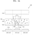
- FIG. 2A illustrates a traveling path of light when the selective transmission member 160 is arranged between the light source array 110 and the color conversion layer 130, according to an embodiment.
- the light source array 110 may be assumed to perform local dimming for each light source.
- a size of local dimming may be a certain range including one light source 112.
- the size of local dimming may also be a certain range including a plurality of light sources 112.
- one light source 112 of the light source array 110 may be in an on state where the light is emitted, and another light source 112 that is adjacent to the light source 112 may be in an off state where the light is not emitted.
- the light source 112 emitting light may be referred to as an on-light source 112a, and the light source 112 that does not emit light may be referred to as an off-light source 112b.
- a region in which an image is generated using light mainly emitted from the on-light source 112a to correspond to the on-light source 112a of the display apparatus 100 may be referred to as a dimming-on region 210, and a region corresponding to the off-light source 112b may be referred to as a dimming-off region 220.
- the light emitted from the on-light source 112a may be incident to the color conversion layer 130 by passing through the selective transmission member 160. A part of the light may go to the display panel 140 by passing through the color conversion layer 130. A partial light may be incident to the color conversion particles 134 and 136 scattered in the color conversion layer 130. The light incident on the first color conversion particles 134 may be converted into green light L G , and the light incident on the second color conversion particles 136 may be converted into red light L R . Thus, the color conversion layer 130 may emit white light Lw including blue light L B , green light L G , and red light L R .
- the partial converted green light L G or red light L R may go to the selective transmission member 160.
- the converted green light L G or red light L R incident to the selective transmission member 160 may be totally reflected from the selective transmission member 160 and emitted toward the display panel 140.
- a traveling space of the converted green light L G or red light L R may be limited in the color conversion layer 130, such that the converted green light L G or red light L R may go relatively short in the color conversion layer 130 and thus may be emitted to the display panel 140.
- a probability of the converted green light L G or red light L R being emitted in the color conversion layer 130 overlapping with the off-light source 112b is low.
- a contrast ratio may be improved in local dimming.
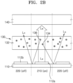
- FIG. 2B illustrates a traveling path of light when a selective transmission member is not arranged between a light source array and a color conversion layer, according to an embodiment, which is not according to the claims.
- the light L B emitted from the on-light source 112a may be incident to the color conversion layer 130.
- a part of the light L B may go to the display panel 140 by passing through the color conversion layer 130.
- a part of the light L B may be incident to the color conversion particles 134 and 136 scattered in the color conversion layer 130.
- the light L B incident to the first color conversion particles 134 may be converted into the green light L G
- the light L B incident to the second color conversion particles 136 may be converted into red light L R .
- the color conversion layer 130 may emit white light Lw including blue light L B , green light L G , and red light L R .
- the converted green light L G and red light L R may go to the light source array 110. Due to absence of the selective transmission member 160, the converted light L G and light L R may go to the light source array 110, may be reflected from the light source array 110 and the substrate, and may be incident again to the color conversion layer 130 overlapping with the off-light source 112b, thus going to the display panel 140. In spite of local dimming, the green light L G and the red light L R may pass through a region of the display panel 140 corresponding to the off-light source 112b, which may be noise degrading a contrast ratio of a color.
- the selective transmission member 160 may prevent light from going to the region of the display panel 140 in a dimming-off region in local dimming, thereby effectively controlling luminance.
- a refractive index and a thickness of each material layer may be determined such that a transmissivity and a reflectivity change with an incidence angle.
- a refractive index and a thickness of each material layer may be designed such that for an incidence angle of 0 degree, a transmissivity is highest, and a transmissivity decreases and a reflectivity increases as the incidence angle increases.
- a refractive index, a thickness, etc., of each material layer may be designed such that a transmittivity of a region of the selective transmission member 160, which overlaps with the light-emitting light source 112, may be higher than that of a region of the selective transmission member 160, which does not overlap with the light-emitting light source 112 and a reflectivity of the region of the selective transmission member 160, which overlaps with the light-emitting light source 112, may be lower than that of the region of the selective transmission member 160, which does not overlap with the light-emitting light source 112.
- a refractive index, a thickness, etc., of each material layer may be designed such that light incident on the selective transmission member 160 at a certain angle or more has a reflectivity higher than a transmissivity.
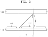
- the certain angle may be determined by a dimming size S of the light source array 110 and a distance D between the light source array 110 and the selective transmission member 160.
- FIG. 3 is a reference view for describing a relationship between a particular angle and a dimming size, according to an embodiment.
- the size S of local dimming may be a certain range including one light source 112, as shown in FIG. 3 .
- a tangent of a certain angle ⁇ may the size S of local dimming with respect to the distance D between the selective transmission member 160 and the light source substrate 120.
- the light incident at the certain angle ⁇ has a transmissivity higher than a reflectivity, whereas light incident at an angle larger than the certain angle ⁇ may have a reflectivity higher than a transmissivity.
- more light emitted from the light source 112 overlapping with the selective transmission member 160 may be incident to the color conversion layer 130, and less light emitted from the light source 112 not overlapping with the selective transmission member 160 may be incident to the color conversion layer 130, thereby more effectively implementing local dimming.
- a transmissivity of light emitted from a region of the light source 112 not overlapping with the selective transmission member 160 may be less than or equal to about 30% of a transmissivity of light emitted from a region of the light source 112 overlapping with the selective transmission member 160.
- light transmission or non-transmission of the selective transmission member 160 may vary with a wavelength of light incident thereto, and a transmittivity and a reflectivity change with an incidence angle, such that luminance control may be effective and color definition may be improved when the light source array 110 operates with a local dimming signal.
- the display apparatus 100 may also include various optical members that adjust a traveling path of light.
- the display apparatus 100 may further include a diffusion plate that diffuses white light emitted from a backlight unit to make overall color and brightness of an image displayed on the display panel 140 uniform, a prism sheet that increases luminance by refracting or gathering the light diffused by the diffusion plate, a dual brightness enhancement film that enhances light gathering power by using polarization characteristics.
- the display apparatus 100 may also include a heat radiating plate that removes heat generated in the light source 112.
- FIG. 4 illustrates a display apparatus 100 including a plurality of selective transmission members 160 and 170, according to an embodiment.
- the color conversion layer 130 in FIG. 4 may include a first color conversion layer 130a including the plurality of first color conversion particles 134 that convert blue light L B into green light L G and a second color conversion layer 130b including the plurality of second color conversion particles 136 that convert at least one of blue light L B or green light L G into red light L R .
- the selective transmission member 160 may be arranged between the light source array 110 and the first color conversion layer 130a.
- the selective transmission member 160 may transmit light incident from the light source array 110 to the first color conversion layer 130a, and may not transmit converted light incident from the first color conversion layer 130a, i.e., the red light L R .
- the selective transmission member 160 may be identical to the selective transmission member 160 described above with reference to FIG. 1 .
- another selective transmission member 170 may be further arranged between the first color conversion layer 130a and the second color conversion layer 130b.
- the selective transmission member 170 may transmit light incident from the first color conversion layer 130a, e.g., the blue light L B and the green light L G to the second color conversion layer 130b, and may not transmit the light converted in the second color conversion layer 130b, i.e., the red light L R .
- traveling paths of the green light L G and the red light L R respectively in the first color conversion layer 130a and the second color conversion layer 130b are short, such that a probability of light going to the dimming-off region 220 may be reduced.
- FIG. 5 illustrates a display apparatus 100 according to an embodiment.
- a color conversion layer 130c of FIG. 5 may include a plurality of barriers 138 arranged spaced apart from each other in the color conversion layer 130c.
- the plurality of barriers 138 may be parallel with an arrangement direction of the light sources 112 of the light source array 110.
- the barrier 138 may be arranged in a region of the color conversion layer 130c, which does not overlap with the light sources 112, to partition a local dimming region. Although it is illustrated that the barrier 138 is arranged for each light source 112, the disclosure is not limited thereto. When a plurality of light sources are grouped to define a local dimming region, the barrier 138 may be arranged spaced in the unit of a plurality of grouped light sources. The barrier 138 may include a reflective material. Hence, a light density of the dimming-on region 210 of the color conversion layer 130 may be improved.
- FIG. 6 illustrates a display apparatus 100 including an electro-optic layer 180 according to an embodiment.
- the display apparatus 100 may further include the electro-optic layer 180 capable of adjusting a transmissivity with respect to the selective transmission member 160 based on optical characteristics thereof that change with an applied electric signal.
- the electro-optic layer 180 may include a plurality of electro-optic particles having optical characteristics that change with an electric signal.
- the display apparatus 100 may further include an electrode part 190 that applies an electric signal to the electro-optic layer 180.
- the electrode part 190 may include a plurality of electrode pairs 192 and 194 arranged spaced with the electro-optic layer 180 therebetween.
- the plurality of electrode pairs 192 and 194 may be arranged spaced in the unit of a dimming region.
- each of the plurality of electrode pairs 192 and 194 may be arranged corresponding to each of the plurality of light sources. More specifically, each of the plurality of electrode pairs 192 and 194 may be arranged overlappingly with the corresponding light source 112.
- the electro-optic particles are substances having an electro-optic effect.
- the electro-optic effect is a phenomenon in which optical characteristics change with an electric field, and a refractive index, a phase delay, polarization characteristics, etc., of electro-optic particles may change with presence or absence of an electric field and/or a strength of the electric field.
- the electro-optic particles may include liquid crystal. At least one of a refractive index or polarization characteristics of the liquid crystal may change with presence or absence of an electric field and/or a strength of the electric field.
- a refractive index or polarization characteristics of the liquid crystal may change with presence or absence of an electric field and/or a strength of the electric field.
- PDLC polymer dispersed liquid crystal
- PNLC polymer network liquid crystal
- cholesteric liquid crystal cholesteric liquid crystal
- smectic liquid crystal etc.
- the electro-optic particles may identically refract incident light.
- light incident on the electro-optic particle may be refracted with an identical refractive index regardless of an incidence position, and the light may be refracted in the same direction regardless of the incidence position.
- the electro-optic particles may become transparent. That is, the electro-optic particles may transmit the incident light.
- the electro-optic particles may refract incident light with a different refractive index in a different direction according to a position.
- the light incident on the electro-optic particle may be refracted at a different refractive index according to a position in which the light is incident.
- the electro-optic particle may become opaque. That is, the electro-optic particles may scatter the incident light.
- an electric signal may be applied to an electrode pair arranged on the dimming-on region 210, and an electric signal may not be applied to an electrode pair arranged on the dimming-off region 220.
- Light traveling on the dimming-on region 210 may go straight due to absence of an influence of an electro-optic particle and may be incident to the selective transmission member 160.
- the light traveling on the dimming-off region 220 is incident to the electro-optic layer 180, the light may be scattered by the electro-optic particle.
- the amount of light incident on the selective transmission member 160 may be reduced.
- the electro-optic particle may include an electro-wetting material in addition to liquid crystal.
- Electro-wettability may mean that surface tension of liquid is changed using electricity, and upon application of an electric signal, wettability of an electro-wetting material increases, thus scattering incident light, and unless the electric signal is not applied, the wettability decreases, reducing disturbance of the traveling path of light.
- the electro-optic layer 180 is arranged between the light source array 110 and the selective transmission member 160, the disclosure is not limited thereto.
- FIG. 7 illustrates a display apparatus 100 including the electro-optic layer 180 according to an embodiment.
- the electro-optic layer 180 may be arranged between the color conversion layer 130 and the display panel 140.
- white light Lw may be prevented from being incident to a region of the display panel 140 arranged in the dimming-off region 220.
- a display apparatus capable of performing such local dimming may be implemented in various forms such as a TV, a monitor, a portable multimedia device, a portable communication device, a portable computing device, etc., to visually display an image.
- the display apparatus capable of performing local dimming may be useful for a display apparatus that projects an image to a real environment to implement augmented reality (AR) where the image appears to exist in the real environment, e.g., a head-up display or a see-through display.
- AR augmented reality
- FIG. 8 illustrates an example of a head-up display apparatus 200.
- the head-up display apparatus 200 may include a spatial light modulator 208, an image enlargement member 212 that enlarges an image generated in the spatial light modulator 208, and an image convergence member 230 that converges the enlarged image and an image corresponding to an external environment into a certain space.
- the certain space may be a user's visual organ 10, e.g., a pupil.
- the spatial light modulator 208 may include the above-described display apparatus 100.
- the spatial light modulator 208 according to an embodiment may provide an image by using light sources arranged two-dimensionally, thereby providing an image having a higher resolution than a spatial light modulator of a scanning type. With the head-up display apparatus 200, the user does not need to directly see the spatial light modulator 208 to recognize the image. Thus, the spatial light modulator 208 may be small.
- an image generated in the small spatial light modulator 208 is also small, such that the image enlargement member 212 may enlarge an image generated in the display apparatus 100.
- the image enlargement member 212 may enlarge the image corresponding to a range of an angle of view or field of view.
- the image enlargement member 212 may be an optical member such as a convex lens, etc.
- the image convergence member 230 may change at least one of an optical path of the enlarged image or an optical path of a real environment for convergence into one region, i.e., a user's visual organ 10.
- the image convergence member 230 may include a beam splitter, a transflective film, a fold mirror, an anisotropic mirror, etc.
- a lens may be further arranged between the image convergence member 230 and the user's visual organ 10.
- the lens is arranged close to the visual organ, such that the focal length of the lens may be shorter than the diameter of the lens. As a result, a wide angle of view or field of view may be easily secured.
- the lens may be an anisotropic mirror, more specifically, a polarization-dependent birefringence lens.
- the display apparatus 100 may improve the quality of the image by implementing local dimming, thus being useful for a head-up display apparatus.
- the display apparatus may improve a contrast ratio by local dimming.
- an image having a high resolution and an enhanced contrast ratio may be provided.
Landscapes
- Physics & Mathematics (AREA)
- Nonlinear Science (AREA)
- General Physics & Mathematics (AREA)
- Optics & Photonics (AREA)
- Mathematical Physics (AREA)
- Crystallography & Structural Chemistry (AREA)
- Chemical & Material Sciences (AREA)
- Control Of Indicators Other Than Cathode Ray Tubes (AREA)
- Devices For Indicating Variable Information By Combining Individual Elements (AREA)
- Led Device Packages (AREA)
- Liquid Crystal (AREA)
- Preparation Of Compounds By Using Micro-Organisms (AREA)
- Measuring Pulse, Heart Rate, Blood Pressure Or Blood Flow (AREA)
- Compounds Of Unknown Constitution (AREA)
Description
- This application is based on and claims priority under 35 U.S.C. § 119 to
Korean Patent Application No. 10-2019-0149894, filed on November 20, 2019 - The disclosure relates to a display apparatus, and more particularly, to a display apparatus capable of performing local dimming.
- A display apparatus that displays an image is an apparatus that uses a display panel to display the image and is used in various devices such as televisions (TVs), computer monitors, smartphones, etc. However, a general display apparatus needs a backlight unit including a separate light source because it is not capable of self-emitting light, and the display panel locates the backlight unit at the rear of a liquid crystal display (LCD).
- The backlight unit is a dimming device that irradiates light uniformly over the entire display panel, and a display panel including a general backlight unit uses a light-emitting diode (LED) of a certain color as a light source.
- Meanwhile, the backlight unit includes a light guide plate that diffuses light, thus uniformly emitting light. However, there is a limitation in achieving local dimming that differentiates a brightness according to a position.
-
US 20190285950 discloses a display that may have a pixel array such as a liquid crystal pixel array. The pixel array may be illuminated with backlight illumination from a backlight unit. The backlight unit may include a printed circuit board, a plurality of light-emitting diodes mounted on the printed circuit board, at least one light spreading layer formed over the printed circuit board that spreads light received from the plurality of light-emitting diodes, a partially reflective layer formed over the at least one light spreading layer, a color conversion layer formed over the partially reflective layer, a collimating layer formed over the color conversion layer, a brightness enhancement film formed over the collimating layer, and a diffuser formed over the brightness enhancement film. The at least one light spreading layer may include two light spreading layers with elongated protrusions that are rotated relative to each other.US 2018/120639 A1 discloses a display device with a direct type backlight adapted for local dimming by the addition of a pixelated liquid crystal shutter between the light sources and the display panel. - Embodiments of the disclosure provide a display apparatus capable of performing local dimming to improve a contrast ratio.
- Additional aspects will be set forth in part in the description which follows and, in part, will be apparent from the description, or may be learned by practice of the presented embodiments of the disclosure.
- According to an aspect, there is provided a display apparatus as set out in
claim 1. Optional features are set out in the dependent claims. - The above and other aspects, features, and advantages of certain embodiments of the present disclosure will be more apparent from the following description taken in conjunction with the accompanying drawings, in which:
-
FIG. 1 illustrates an example of a display apparatus according to an embodiment; -
FIG. 2A illustrates a traveling path of light when a selective transmission member is arranged between a light source array and a color conversion layer, according to an embodiment; -
FIG. 2B illustrates a traveling path of light when a selective transmission member is not arranged between a light source array and a color conversion layer, according to an embodiment, which is not according to the claims; -
FIG. 3 is a reference view for describing a relationship between a particular angle and a dimming size, according to an embodiment; -
FIG. 4 illustrates a display apparatus including a plurality of selective transmission members, according to an embodiment; -
FIG. 5 illustrates a display apparatus according to an embodiment; -
FIG. 6 illustrates a display apparatus including an electro-optic layer, according to an embodiment; -
FIG. 7 illustrates a display apparatus including an electro-optic layer, according to an embodiment; and -
FIG. 8 illustrates a head-up display apparatus, according to an embodiment. - Hereinafter, a display apparatus according to various embodiments of the disclosure will be disclosed with reference to the accompanying drawings. The width and thickness of layers or regions illustrated in the accompanying drawings may be exaggerated for clarity of the specification and convenience of explanation. Throughout the detailed description, identical reference numerals refer to identical elements.
- Terms such as "comprise" and "include" used in the embodiments of the disclosure should not be interpreted as including all of elements or operations described herein, and should be interpreted as excluding some of the elements or operations or as further including additional elements or operations.
- Throughout the disclosure, the expression "at least one of a, b or c" indicates only a, only b, only c, both a and b, both a and c, both b and c, all of a, b, and c, or variations thereof.
- Hereinbelow, an expression such as "above" or "on" may include not only the meaning of "immediately on/under/to the left/to the right in a contact manner", but also the meaning of "on/under/to the left/to the right in a non-contact manner". Hereinafter, embodiments of the disclosure of the disclosure will be described in detail for illustration with reference to the accompanying drawings.
- Terms such as first, second, and the like may be used to describe various elements, but the elements should not be limited to those terms. These terms may be used for the purpose of distinguishing one element from another element.
-
FIG. 1 illustrates an example of adisplay apparatus 100 according to an embodiment. - Referring to
FIG. 1 , thedisplay apparatus 100 includes alight source array 110 in which a plurality oflight sources 112 are arranged, acolor conversion layer 130 that emits white light LW by using light emitted from thelight source array 110, and adisplay panel 140 that outputs an image by using the white light LW. - In the
light source array 110, the plurality oflight sources 112 may be arranged two-dimensionally. Each of the plurality oflight sources 112 may emit light. Thelight source 112 may include a light-emitting diode (LED). The LED may be provided in the form of a package in which an LED chip is mounted on a substrate and resin is filled. However, unlike in the current embodiment of the disclosure, as thelight source 112, a cold cathode fluorescent lamp (CCFL) or an external electrode fluorescent lamp (EEFL) may be used. - The
light source 112 may emit light of a certain color. Herein, the light of the certain color may include light in blue. The light in blue may mean light that has a wavelength of about 400 nm to about 500 nm and is visually seen as blue. Thelight source 112 may be implemented using a blue light-emitting diode to emit light in blue. - The plurality of
light sources 112 may be arranged spaced at certain intervals on alight source substrate 120. Thelight source substrate 120 may include a light source controller connected with thelight source 112. The light source controller may analyze an image displayed on thedisplay panel 140 to output a local dimming signal and control a luminance of light generated by thelight source 112 in response to the local dimming signal. For example, the light source controller may independently control the plurality oflight sources 112 and group the plurality oflight sources 112 to control each group of thelight sources 112. In an embodiment, the light source controller may be provided as being mounted on a separate circuit board and a position thereof is not specially limited. - The
color conversion layer 130 may include abase layer 132 and a plurality ofcolor conversion particles base layer 132 and convert the light into light having a certain color. - The
base layer 132 may be formed of a transparent polymer material. For example, thebase layer 132 may be transparent cure resin. - Each of the plurality of
color conversion particles - When the light incident on the
color conversion layer 130 has enough energy to excite thecolor conversion particles color conversion particles color conversion particles color conversion layer 130. - For example, according to a particle size of a color conversion particle, the color of the light radiated from the color conversion particle may be determined. Overall, for a large particle size, light having a long wavelength may be generated, and for a small particle size, light having a short wavelength may be generated.
- According to the current embodiment of the disclosure, each of the
color conversion particles 134 and 135 may include a quantum dot (QD). The light emitted from thecolor conversion particles color conversion layer 130 may be radiated in various directions. - For example, the plurality of
color conversion particles color conversion particles 134 and a plurality of secondcolor conversion particles 136. Each of the firstcolor conversion particles 134 may absorb light having a first wavelength band and convert the absorbed light into light having a second wavelength band. A central wavelength of the second wavelength band may be greater than that of the first wavelength band. For example, the first wavelength band may be about 400 nm to about 500 nm, and the second wavelength band may be about 480 nm to about 560 nm. That is, each of the firstcolor conversion particles 134 may substantially convert blue light LB into green light LG. - Each of the second
color conversion particles 136 may absorb the light having the first wavelength band and convert the absorbed light into light having a third wavelength band. A central wavelength of the third wavelength band may be less than that of the second wavelength band. For example, the third wavelength band may be about 640 nm to about 780 nm. That is, each of the secondcolor conversion particles 136 may substantially convert blue light LB into red light LR. - As described above, according to the size of each of the
color conversion particles color conversion particles color conversion particles 134 may be less than that of each of the secondcolor conversion particles 136. - Although not shown, the
color conversion layer 130 may further include scattering devices. The scattering devices may be mixed with the firstcolor conversion particles 134 and the secondcolor conversion particles 136. - The
display panel 140 may be provided in front of thecolor conversion layer 130 and block or transmit the light emitted from thecolor conversion layer 130 to form an image. Thedisplay panel 140 may be, for example, a liquidcrystal display panel 140. - The
display panel 140 may include a plurality of pixels. The plurality of pixels included in thedisplay panel 140 may independently block or transmit the light emitted from thecolor conversion layer 130, and the light passing through the plurality of pixels may form an image. For example, to implement the plurality of pixels, thedisplay panel 140 may include a first polarization film, a transparent substrate, a pixel electrode, a thin film transistor, a liquid crystal layer, a common electrode, a color filter, etc. - A
control assembly 150 may include a control circuit that controls operations of thedisplay panel 140 and thelight source array 110. The control circuit may process image data received from an external content source and transmit the image data to thedisplay panel 140. - The
display apparatus 100 further includes aselective transmission member 160 that is arranged between thelight source array 110 and thecolor conversion layer 130, transmits light incident from thelight source array 110 through thecolor conversion layer 130, and does not transmit the light converted in thecolor conversion layer 130 toward thelight source array 110. Theselective transmission member 160 may totally reflect the light converted in thecolor conversion layer 130 when the converted light is incident thereon. - The
selective transmission member 160 may have optical properties including a plurality of different material layers. Incident light satisfying a certain condition may be totally reflected by interaction between the plurality of material layers and the incident light. For example, on an interfacial face between media having different refractive indices, light is refracted and reflected and passes, in which a total amount of reflected light and a total amount of transmitted light may be determined by interference between reflected light and transmitted light in multiple paths caused by a plurality of interfacial faces. - By considering such interference, a refractive index and a thickness of each layer may be determined to totally reflect the light satisfying the certain condition. Based on that the optical properties depend on a wavelength of incident light, the
selective transmission member 160 may be designed to totally reflect light having a certain wavelength band, which is incident at a set reference angle, in which a transmissivity and a reflectivity vary with an incidence angle for light having other a different wavelength. Theselective transmission member 160 may be referred to as, but not limited to, a dichroic filter. - The refractive index and thickness of the material layer may be determined such that the
selective transmission member 160 according to an embodiment transmits light incident from thelight source array 110 to thecolor conversion layer 130 and does not transmit the light converted in thecolor conversion layer 130 to thelight source array 110. For example, the blue light LB may be emitted to thelight source array 110, whereas the light converted in thecolor conversion layer 130 may be green light LG or red light LR. Thus, theselective transmission member 160 may selectively transmit or reflect the light according to a wavelength of the incident light. -
FIG. 2A illustrates a traveling path of light when theselective transmission member 160 is arranged between thelight source array 110 and thecolor conversion layer 130, according to an embodiment. To facilitate convenience of a description, thelight source array 110 may be assumed to perform local dimming for each light source. Then, a size of local dimming may be a certain range including onelight source 112. However, the disclosure is not limited thereto. The size of local dimming may also be a certain range including a plurality oflight sources 112. - As shown in
FIG. 2A , onelight source 112 of thelight source array 110 may be in an on state where the light is emitted, and anotherlight source 112 that is adjacent to thelight source 112 may be in an off state where the light is not emitted. Thelight source 112 emitting light may be referred to as an on-light source 112a, and thelight source 112 that does not emit light may be referred to as an off-light source 112b. A region in which an image is generated using light mainly emitted from the on-light source 112a to correspond to the on-light source 112a of thedisplay apparatus 100 may be referred to as a dimming-onregion 210, and a region corresponding to the off-light source 112b may be referred to as a dimming-off region 220. - The light emitted from the on-
light source 112a may be incident to thecolor conversion layer 130 by passing through theselective transmission member 160. A part of the light may go to thedisplay panel 140 by passing through thecolor conversion layer 130. A partial light may be incident to thecolor conversion particles color conversion layer 130. The light incident on the firstcolor conversion particles 134 may be converted into green light LG, and the light incident on the secondcolor conversion particles 136 may be converted into red light LR. Thus, thecolor conversion layer 130 may emit white light Lw including blue light LB, green light LG, and red light LR. - Meanwhile, the partial converted green light LG or red light LR may go to the
selective transmission member 160. The converted green light LG or red light LR incident to theselective transmission member 160 may be totally reflected from theselective transmission member 160 and emitted toward thedisplay panel 140. A traveling space of the converted green light LG or red light LR may be limited in thecolor conversion layer 130, such that the converted green light LG or red light LR may go relatively short in thecolor conversion layer 130 and thus may be emitted to thedisplay panel 140. Thus, a probability of the converted green light LG or red light LR being emitted in thecolor conversion layer 130 overlapping with the off-light source 112b is low. Hence, a contrast ratio may be improved in local dimming. -
FIG. 2B illustrates a traveling path of light when a selective transmission member is not arranged between a light source array and a color conversion layer, according to an embodiment, which is not according to the claims. As shown inFIG. 2B , the light LB emitted from the on-light source 112a may be incident to thecolor conversion layer 130. A part of the light LB may go to thedisplay panel 140 by passing through thecolor conversion layer 130. A part of the light LB may be incident to thecolor conversion particles color conversion layer 130. The light LB incident to the firstcolor conversion particles 134 may be converted into the green light LG, and the light LB incident to the secondcolor conversion particles 136 may be converted into red light LR. Thus, thecolor conversion layer 130 may emit white light Lw including blue light LB, green light LG, and red light LR. - Meanwhile, a part of the converted green light LG and red light LR may go to the
light source array 110. Due to absence of theselective transmission member 160, the converted light LG and light LR may go to thelight source array 110, may be reflected from thelight source array 110 and the substrate, and may be incident again to thecolor conversion layer 130 overlapping with the off-light source 112b, thus going to thedisplay panel 140. In spite of local dimming, the green light LG and the red light LR may pass through a region of thedisplay panel 140 corresponding to the off-light source 112b, which may be noise degrading a contrast ratio of a color. - Thus, the
selective transmission member 160 may prevent light from going to the region of thedisplay panel 140 in a dimming-off region in local dimming, thereby effectively controlling luminance. - Even the
selective transmission member 160 passes through light incident from thelight source array 110, a refractive index and a thickness of each material layer may be determined such that a transmissivity and a reflectivity change with an incidence angle. For example, a refractive index and a thickness of each material layer may be designed such that for an incidence angle of 0 degree, a transmissivity is highest, and a transmissivity decreases and a reflectivity increases as the incidence angle increases. - Alternatively, a refractive index, a thickness, etc., of each material layer may be designed such that a transmittivity of a region of the
selective transmission member 160, which overlaps with the light-emittinglight source 112, may be higher than that of a region of theselective transmission member 160, which does not overlap with the light-emittinglight source 112 and a reflectivity of the region of theselective transmission member 160, which overlaps with the light-emittinglight source 112, may be lower than that of the region of theselective transmission member 160, which does not overlap with the light-emittinglight source 112. - Alternatively, a refractive index, a thickness, etc., of each material layer may be designed such that light incident on the
selective transmission member 160 at a certain angle or more has a reflectivity higher than a transmissivity. The certain angle may be determined by a dimming size S of thelight source array 110 and a distance D between thelight source array 110 and theselective transmission member 160. -
FIG. 3 is a reference view for describing a relationship between a particular angle and a dimming size, according to an embodiment. When thelight source array 110 performs local dimming in the unit of thelight source 112, the size S of local dimming may be a certain range including onelight source 112, as shown inFIG. 3 . - A tangent of a certain angle θ may the size S of local dimming with respect to the distance D between the
selective transmission member 160 and thelight source substrate 120.

- The light incident at the certain angle θ has a transmissivity higher than a reflectivity, whereas light incident at an angle larger than the certain angle θ may have a reflectivity higher than a transmissivity. Hence, more light emitted from the
light source 112 overlapping with theselective transmission member 160 may be incident to thecolor conversion layer 130, and less light emitted from thelight source 112 not overlapping with theselective transmission member 160 may be incident to thecolor conversion layer 130, thereby more effectively implementing local dimming. For example, a transmissivity of light emitted from a region of thelight source 112 not overlapping with theselective transmission member 160 may be less than or equal to about 30% of a transmissivity of light emitted from a region of thelight source 112 overlapping with theselective transmission member 160. - As such, light transmission or non-transmission of the
selective transmission member 160 may vary with a wavelength of light incident thereto, and a transmittivity and a reflectivity change with an incidence angle, such that luminance control may be effective and color definition may be improved when thelight source array 110 operates with a local dimming signal. - The
display apparatus 100 may also include various optical members that adjust a traveling path of light. For example, thedisplay apparatus 100 may further include a diffusion plate that diffuses white light emitted from a backlight unit to make overall color and brightness of an image displayed on thedisplay panel 140 uniform, a prism sheet that increases luminance by refracting or gathering the light diffused by the diffusion plate, a dual brightness enhancement film that enhances light gathering power by using polarization characteristics. Thedisplay apparatus 100 may also include a heat radiating plate that removes heat generated in thelight source 112. -
FIG. 4 illustrates adisplay apparatus 100 including a plurality ofselective transmission members FIG. 1 withFIG. 4 , thecolor conversion layer 130 inFIG. 4 may include a firstcolor conversion layer 130a including the plurality of firstcolor conversion particles 134 that convert blue light LB into green light LG and a secondcolor conversion layer 130b including the plurality of secondcolor conversion particles 136 that convert at least one of blue light LB or green light LG into red light LR. - The
selective transmission member 160 may be arranged between thelight source array 110 and the firstcolor conversion layer 130a. Theselective transmission member 160 may transmit light incident from thelight source array 110 to the firstcolor conversion layer 130a, and may not transmit converted light incident from the firstcolor conversion layer 130a, i.e., the red light LR. Theselective transmission member 160 may be identical to theselective transmission member 160 described above with reference toFIG. 1 . - Meanwhile, another
selective transmission member 170 may be further arranged between the firstcolor conversion layer 130a and the secondcolor conversion layer 130b. Theselective transmission member 170 may transmit light incident from the firstcolor conversion layer 130a, e.g., the blue light LB and the green light LG to the secondcolor conversion layer 130b, and may not transmit the light converted in the secondcolor conversion layer 130b, i.e., the red light LR. Thus, traveling paths of the green light LG and the red light LR respectively in the firstcolor conversion layer 130a and the secondcolor conversion layer 130b are short, such that a probability of light going to the dimming-off region 220 may be reduced. -
FIG. 5 illustrates adisplay apparatus 100 according to an embodiment. ComparingFIG. 1 withFIG. 5 , acolor conversion layer 130c ofFIG. 5 may include a plurality ofbarriers 138 arranged spaced apart from each other in thecolor conversion layer 130c. The plurality ofbarriers 138 may be parallel with an arrangement direction of thelight sources 112 of thelight source array 110. - The
barrier 138 may be arranged in a region of thecolor conversion layer 130c, which does not overlap with thelight sources 112, to partition a local dimming region. Although it is illustrated that thebarrier 138 is arranged for eachlight source 112, the disclosure is not limited thereto. When a plurality of light sources are grouped to define a local dimming region, thebarrier 138 may be arranged spaced in the unit of a plurality of grouped light sources. Thebarrier 138 may include a reflective material. Hence, a light density of the dimming-onregion 210 of thecolor conversion layer 130 may be improved. -
FIG. 6 illustrates adisplay apparatus 100 including an electro-optic layer 180 according to an embodiment. ComparingFIG. 1 withFIG. 6 , as shown inFIG. 6 , thedisplay apparatus 100 may further include the electro-optic layer 180 capable of adjusting a transmissivity with respect to theselective transmission member 160 based on optical characteristics thereof that change with an applied electric signal. The electro-optic layer 180 may include a plurality of electro-optic particles having optical characteristics that change with an electric signal. - The
display apparatus 100 may further include anelectrode part 190 that applies an electric signal to the electro-optic layer 180. Theelectrode part 190 may include a plurality of electrode pairs 192 and 194 arranged spaced with the electro-optic layer 180 therebetween. The plurality of electrode pairs 192 and 194 may be arranged spaced in the unit of a dimming region. For example, each of the plurality of electrode pairs 192 and 194 may be arranged corresponding to each of the plurality of light sources. More specifically, each of the plurality of electrode pairs 192 and 194 may be arranged overlappingly with the correspondinglight source 112. - The electro-optic particles are substances having an electro-optic effect. The electro-optic effect is a phenomenon in which optical characteristics change with an electric field, and a refractive index, a phase delay, polarization characteristics, etc., of electro-optic particles may change with presence or absence of an electric field and/or a strength of the electric field.
- The electro-optic particles may include liquid crystal. At least one of a refractive index or polarization characteristics of the liquid crystal may change with presence or absence of an electric field and/or a strength of the electric field. For example, polymer dispersed liquid crystal (PDLC), polymer network liquid crystal (PNLC), cholesteric liquid crystal, smectic liquid crystal, etc., may be used as electro-optic particles.
- Upon application of an electric field to the electro-
optic layer 180, the electro-optic particles may identically refract incident light. In other words, light incident on the electro-optic particle may be refracted with an identical refractive index regardless of an incidence position, and the light may be refracted in the same direction regardless of the incidence position. Thus, upon application of an electric field to the electro-optic layer 180, the electro-optic particles may become transparent. That is, the electro-optic particles may transmit the incident light. - When the electric field is not applied to the electro-
optic layer 180, the electro-optic particles may refract incident light with a different refractive index in a different direction according to a position. In other words, the light incident on the electro-optic particle may be refracted at a different refractive index according to a position in which the light is incident. Thus, when the electric field is not applied to the electro-optic particle, the electro-optic particle may become opaque. That is, the electro-optic particles may scatter the incident light. - For example, an electric signal may be applied to an electrode pair arranged on the dimming-on
region 210, and an electric signal may not be applied to an electrode pair arranged on the dimming-off region 220. Light traveling on the dimming-onregion 210 may go straight due to absence of an influence of an electro-optic particle and may be incident to theselective transmission member 160. On the other hand, when the light traveling on the dimming-off region 220 is incident to the electro-optic layer 180, the light may be scattered by the electro-optic particle. Thus, the amount of light incident on theselective transmission member 160 may be reduced. - The electro-optic particle may include an electro-wetting material in addition to liquid crystal. Electro-wettability may mean that surface tension of liquid is changed using electricity, and upon application of an electric signal, wettability of an electro-wetting material increases, thus scattering incident light, and unless the electric signal is not applied, the wettability decreases, reducing disturbance of the traveling path of light.
- While it is illustrated in
FIG. 6 that the electro-optic layer 180 is arranged between thelight source array 110 and theselective transmission member 160, the disclosure is not limited thereto. -
FIG. 7 illustrates adisplay apparatus 100 including the electro-optic layer 180 according to an embodiment. As shown inFIG. 7 , the electro-optic layer 180 may be arranged between thecolor conversion layer 130 and thedisplay panel 140. When the electro-optic layer 180 is arranged between thecolor conversion layer 130 and thedisplay panel 140, white light Lw may be prevented from being incident to a region of thedisplay panel 140 arranged in the dimming-off region 220. - A display apparatus capable of performing such local dimming may be implemented in various forms such as a TV, a monitor, a portable multimedia device, a portable communication device, a portable computing device, etc., to visually display an image. In particular, the display apparatus capable of performing local dimming may be useful for a display apparatus that projects an image to a real environment to implement augmented reality (AR) where the image appears to exist in the real environment, e.g., a head-up display or a see-through display.
-
FIG. 8 illustrates an example of a head-updisplay apparatus 200. As shown inFIG. 8 , the head-updisplay apparatus 200 may include a spatiallight modulator 208, animage enlargement member 212 that enlarges an image generated in the spatiallight modulator 208, and animage convergence member 230 that converges the enlarged image and an image corresponding to an external environment into a certain space. The certain space may be a user'svisual organ 10, e.g., a pupil. - The spatial
light modulator 208 may include the above-describeddisplay apparatus 100. The spatiallight modulator 208 according to an embodiment may provide an image by using light sources arranged two-dimensionally, thereby providing an image having a higher resolution than a spatial light modulator of a scanning type. With the head-updisplay apparatus 200, the user does not need to directly see the spatiallight modulator 208 to recognize the image. Thus, the spatiallight modulator 208 may be small. - Meanwhile, an image generated in the small spatial
light modulator 208 is also small, such that theimage enlargement member 212 may enlarge an image generated in thedisplay apparatus 100. Theimage enlargement member 212 may enlarge the image corresponding to a range of an angle of view or field of view. Theimage enlargement member 212 may be an optical member such as a convex lens, etc. - The
image convergence member 230 may change at least one of an optical path of the enlarged image or an optical path of a real environment for convergence into one region, i.e., a user'svisual organ 10. Theimage convergence member 230 may include a beam splitter, a transflective film, a fold mirror, an anisotropic mirror, etc. - Although not shown, a lens may be further arranged between the
image convergence member 230 and the user'svisual organ 10. The lens is arranged close to the visual organ, such that the focal length of the lens may be shorter than the diameter of the lens. As a result, a wide angle of view or field of view may be easily secured. The lens may be an anisotropic mirror, more specifically, a polarization-dependent birefringence lens. - As such, when the image generated in the small spatial
light modulator 208, i.e., the display apparatus is recognized together with the external environment, brightness and definition of the image may be important factors. Thedisplay apparatus 100 according to an embodiment may improve the quality of the image by implementing local dimming, thus being useful for a head-up display apparatus. - The display apparatus according to an embodiment may improve a contrast ratio by local dimming.
- By applying the display apparatus according to an embodiment to the head-up display apparatus, an image having a high resolution and an enhanced contrast ratio may be provided.
- So far, the disclosure has been described with reference to the embodiments of the disclosure. It would be understood by those of ordinary skill in the art that the disclosure may be implemented in a modified form without departing from the scope of the claims.
Claims (14)
- A display apparatus (100) comprising:a light source array (110) in which a plurality of light sources emitting light and configured to be controlled according to a local dimming driving scheme are arranged;a color conversion layer (130) comprising color conversion particles (134, 136) that convert the emitted light into light of a certain color, and configured to emit white light (LW) by using the converted light;a display panel (140) configured to generate an image by using the white light; anda selective transmission member (160) which is arranged between the light source array and the color conversion layer, and configured to transmit the emitted light to the color conversion layer, and to block light converted in the color conversion layer (130) propagating towards the light source array,wherein a transmissivity of a first region corresponding to a light source, which is configured to emit the light, of the selective transmission member is greater than a transmissivity of a second region not corresponding to the light source, of the selective transmission member.
- The display apparatus of claim 1, wherein the selective transmission member totally reflects the converted light incident thereon.
- The display apparatus of claim 1 or 2, wherein the selective transmission member comprises a transmissivity and a reflectivity that change with an incidence angle of the light.
- The display apparatus of claim 3, wherein, for light that is incident on the selective transmission member at an incidence angle equal to or greater than a certain angle, the reflectivity of the selective transmission member is greater than the transmissivity of the selective transmission member.
- The display apparatus of claim 4, wherein the certain angle is determined based on a size of a local dimming area and a distance between the light source array and the selective transmission member.
- The display apparatus of claim 5, wherein the first region comprises a region overlapping with the light source that emits the light.
- The display apparatus of any one of the preceding claims, wherein the transmissivity of light of the second region is less than or equal to 30% of the transmissivity of light of the first region.
- The display apparatus of any one of the preceding claims, wherein the selective transmission member comprises a combination of a plurality of material layers having different refractive indices.
- The display apparatus of any one of the preceding claims, wherein the color conversion layer further comprises a plurality of barriers (138) arranged spaced in parallel in a direction in which the plurality of light sources are arranged in the color conversion layer.
- The display apparatus of claim 9, wherein the plurality of barriers are arranged in a region of the color conversion layer that does not overlap with the plurality of light sources.
- The display apparatus of any one of the preceding claims, wherein the color conversion layer further comprises:a first color conversion layer (130a) comprising first color conversion particles (134) that convert blue light into green light; anda second color conversion layer (130b) comprising second color conversion particles (136) that convert the blue light into red light.
- The display apparatus of claim 11, further comprising:another selective transmission member (170) arranged between the first color conversion layer and the second color conversion layer, and configured to transmit the blue light and the green light and reflect the red light,wherein the second color conversion layer is disposed between the another selective transmission member and the display panel.
- The display apparatus of any one of the preceding claims, further comprising:an electro-optic layer (180) configured to adjust the amount of light that is incident on the selective transmission member, based on optical characteristics thereof that change with an applied electric signal; andan electrode part configured to apply the applied electric signal to the electro-optic layer.
- The display apparatus of any one of the preceding claims, further comprising:an image enlargement member (212) configured to enlarge the image generated in the display panel; andan image convergence member (230) configured to converge the enlarged image and an image corresponding to an external environment into a certain space.
Applications Claiming Priority (1)
| Application Number | Priority Date | Filing Date | Title |
|---|---|---|---|
| KR1020190149894A KR102927816B1 (en) | 2019-11-20 | 2019-11-20 | Display apparatus |
Publications (3)
| Publication Number | Publication Date |
|---|---|
| EP3835857A2 EP3835857A2 (en) | 2021-06-16 |
| EP3835857A3 EP3835857A3 (en) | 2021-09-01 |
| EP3835857B1 true EP3835857B1 (en) | 2023-06-21 |
Family
ID=73497690
Family Applications (1)
| Application Number | Title | Priority Date | Filing Date |
|---|---|---|---|
| EP20208756.5A Active EP3835857B1 (en) | 2019-11-20 | 2020-11-19 | Display apparatus |
Country Status (4)
| Country | Link |
|---|---|
| US (1) | US11460695B2 (en) |
| EP (1) | EP3835857B1 (en) |
| KR (1) | KR102927816B1 (en) |
| CN (1) | CN112824959B (en) |
Families Citing this family (5)
| Publication number | Priority date | Publication date | Assignee | Title |
|---|---|---|---|---|
| CN117751402A (en) * | 2021-07-30 | 2024-03-22 | 3M创新有限公司 | Optical film and display system including the same |
| CN116259699B (en) * | 2021-12-09 | 2026-06-26 | 厦门市芯颖显示科技有限公司 | A display device and display |
| KR102822054B1 (en) * | 2021-12-27 | 2025-06-18 | 한국광기술원 | Stackable Color Filters and Display Apparatus Including the Same |
| WO2023150045A1 (en) * | 2022-02-07 | 2023-08-10 | Corning Incorporated | Reflective and transflective displays including quantum dot layers |
| CN116594221A (en) * | 2023-05-16 | 2023-08-15 | 业桓科技(成都)有限公司 | Light conversion film structure, backlight module and display device |
Family Cites Families (28)
| Publication number | Priority date | Publication date | Assignee | Title |
|---|---|---|---|---|
| US6160666A (en) * | 1994-02-07 | 2000-12-12 | I-O Display Systems Llc | Personal visual display system |
| US8921473B1 (en) | 2004-04-30 | 2014-12-30 | Sydney Hyman | Image making medium |
| US9744800B2 (en) | 1999-06-11 | 2017-08-29 | Sydney Hyman | Compositions and image making mediums |
| JP2001083601A (en) * | 1999-09-16 | 2001-03-30 | Ricoh Co Ltd | Projector device |
| JP2007225776A (en) * | 2006-02-22 | 2007-09-06 | Konica Minolta Opto Inc | Image projecting device |
| JP2008041361A (en) * | 2006-08-03 | 2008-02-21 | Idemitsu Kosan Co Ltd | Fluorescence conversion medium and color light emitting device including the same |
| CN100502065C (en) * | 2006-10-09 | 2009-06-17 | 李屹 | High-efficiency fluorescent conversion LED light source and backlight module |
| CN101609230B (en) * | 2008-06-18 | 2011-12-14 | 鸿富锦精密工业(深圳)有限公司 | Backlight module |
| GB2464102A (en) * | 2008-10-01 | 2010-04-07 | Optovate Ltd | Illumination apparatus comprising multiple monolithic subarrays |
| KR101178723B1 (en) * | 2009-12-30 | 2012-08-31 | 제일모직주식회사 | Multi-layered light diffuser plate for back light unit of lcd and back light unit comprising the same |
| KR20130015847A (en) * | 2011-08-05 | 2013-02-14 | 삼성전자주식회사 | Light emitting device, backlight unit and display apparatus using the same, and manufacturing method of the same |
| US20150323711A1 (en) * | 2012-11-30 | 2015-11-12 | Sharp Kabushiki Kaisha | Scatterer substrate |
| CN104854717B (en) * | 2012-12-05 | 2017-11-28 | 飞利浦照明控股有限公司 | Color conversion devices, lighting units, solid state light emitter packages and lamps |
| US10037689B2 (en) | 2015-03-24 | 2018-07-31 | Donald Warren Taylor | Apparatus and system to manage monitored vehicular flow rate |
| KR20150134926A (en) * | 2014-05-23 | 2015-12-02 | 주식회사 창강화학 | Quantum dot Film, Display Including Same and Manufacturing method of Quantum dot Film |
| KR102239112B1 (en) * | 2014-07-30 | 2021-04-13 | 삼성디스플레이 주식회사 | Display device |
| US9989763B2 (en) | 2015-12-04 | 2018-06-05 | Microsoft Technology Licensing, Llc | Imaging using multiple different narrow bands of light having respective different emission peaks |
| KR101975350B1 (en) * | 2016-04-18 | 2019-05-07 | 주식회사 엘지화학 | Color conversion film and backlight unit and display apparatus comprising the same |
| US10109054B1 (en) | 2016-07-19 | 2018-10-23 | Rockwell Collins, Inc. | Monitoring COTS display devices for HWD/HUD/EVS via transparent photodetectors and imagers |
| US10459289B2 (en) | 2016-11-02 | 2019-10-29 | Innolux Corporation | Display device |
| CN111983850B (en) * | 2016-11-02 | 2023-11-07 | 群创光电股份有限公司 | display device |
| KR102740164B1 (en) * | 2016-11-14 | 2024-12-10 | 삼성전자주식회사 | Back light unit and display apparatus comprising the same |
| US10988686B2 (en) * | 2017-06-02 | 2021-04-27 | Nexdot | Luminescent particles comprising encapsulated nanoparticles and uses thereof |
| JP6966225B2 (en) * | 2017-06-02 | 2021-11-10 | スリーエム イノベイティブ プロパティズ カンパニー | Direct backlight |
| US11112685B2 (en) * | 2017-06-02 | 2021-09-07 | Nexdot | Color conversion layer and display apparatus having the same |
| CN107132697A (en) * | 2017-07-18 | 2017-09-05 | 京东方科技集团股份有限公司 | A kind of backlight module and display device |
| GB201718307D0 (en) * | 2017-11-05 | 2017-12-20 | Optovate Ltd | Display apparatus |
| EP3765896A1 (en) | 2018-03-13 | 2021-01-20 | Apple Inc. | Displays with direct-lit backlight units |
-
2019
- 2019-11-20 KR KR1020190149894A patent/KR102927816B1/en active Active
-
2020
- 2020-11-06 US US17/091,591 patent/US11460695B2/en active Active
- 2020-11-13 CN CN202011267377.5A patent/CN112824959B/en active Active
- 2020-11-19 EP EP20208756.5A patent/EP3835857B1/en active Active
Also Published As
| Publication number | Publication date |
|---|---|
| EP3835857A3 (en) | 2021-09-01 |
| KR102927816B1 (en) | 2026-02-12 |
| KR20210061858A (en) | 2021-05-28 |
| US20210149193A1 (en) | 2021-05-20 |
| CN112824959B (en) | 2024-07-09 |
| EP3835857A2 (en) | 2021-06-16 |
| US11460695B2 (en) | 2022-10-04 |
| CN112824959A (en) | 2021-05-21 |
Similar Documents
| Publication | Publication Date | Title |
|---|---|---|
| US11460695B2 (en) | Display apparatus | |
| JP6403216B2 (en) | Suppression of crosstalk in directional backlight | |
| KR101518734B1 (en) | Back light unit providing polarized light and display apparatus employing the back light unit | |
| JP5304992B2 (en) | Display device | |
| JP4757577B2 (en) | Light source device, display device, terminal device, light source unit, and driving method of light source device | |
| US8368639B2 (en) | Planar light source device, display device, terminal device, and method for driving planar light source device | |
| JP3457591B2 (en) | Liquid crystal display | |
| EP0901033B1 (en) | Panel light source device and display comprising it | |
| US9581749B2 (en) | Lighting unit, display, and three-dimensional display | |
| US12038644B2 (en) | Light source apparatus and information display system using the same | |
| WO2009084176A1 (en) | Illuminating device and liquid crystal display device | |
| JP2022545685A (en) | Directional lighting and privacy displays | |
| EP2450742B1 (en) | Backlight source and thinning method for the same and liquid crystal device with the same | |
| JP4314890B2 (en) | Liquid crystal display | |
| JP2007279224A (en) | Liquid crystal display | |
| EP3825760B1 (en) | Backlight unit and display apparatus comprising same | |
| JP2011221196A (en) | Fiber-shaped light modulation element, illuminating device, and display device | |
| US11385398B2 (en) | Backlight unit and display apparatus having the same | |
| CN224232082U (en) | Backlight module and display device | |
| CN120406006A (en) | Backlight module and display device | |
| KR19990037940U (en) | Reflective liquid crystal display device | |
| WO2022177606A1 (en) | Backlight unit with emission modification | |
| TWM565320U (en) | Light guide film, backlight module and display device |
Legal Events
| Date | Code | Title | Description |
|---|---|---|---|
| PUAI | Public reference made under article 153(3) epc to a published international application that has entered the european phase |
Free format text: ORIGINAL CODE: 0009012 |
|
| STAA | Information on the status of an ep patent application or granted ep patent |
Free format text: STATUS: THE APPLICATION HAS BEEN PUBLISHED |
|
| AK | Designated contracting states |
Kind code of ref document: A2 Designated state(s): AL AT BE BG CH CY CZ DE DK EE ES FI FR GB GR HR HU IE IS IT LI LT LU LV MC MK MT NL NO PL PT RO RS SE SI SK SM TR |
|
| PUAL | Search report despatched |
Free format text: ORIGINAL CODE: 0009013 |
|
| AK | Designated contracting states |
Kind code of ref document: A3 Designated state(s): AL AT BE BG CH CY CZ DE DK EE ES FI FR GB GR HR HU IE IS IT LI LT LU LV MC MK MT NL NO PL PT RO RS SE SI SK SM TR |
|
| RIC1 | Information provided on ipc code assigned before grant |
Ipc: G02F 1/1335 20060101AFI20210727BHEP Ipc: G02F 1/13357 20060101ALI20210727BHEP Ipc: G02F 1/1347 20060101ALI20210727BHEP |
|
| STAA | Information on the status of an ep patent application or granted ep patent |
Free format text: STATUS: REQUEST FOR EXAMINATION WAS MADE |
|
| 17P | Request for examination filed |
Effective date: 20211119 |
|
| RBV | Designated contracting states (corrected) |
Designated state(s): AL AT BE BG CH CY CZ DE DK EE ES FI FR GB GR HR HU IE IS IT LI LT LU LV MC MK MT NL NO PL PT RO RS SE SI SK SM TR |
|
| GRAP | Despatch of communication of intention to grant a patent |
Free format text: ORIGINAL CODE: EPIDOSNIGR1 |
|
| STAA | Information on the status of an ep patent application or granted ep patent |
Free format text: STATUS: GRANT OF PATENT IS INTENDED |
|
| INTG | Intention to grant announced |
Effective date: 20230317 |
|
| GRAS | Grant fee paid |
Free format text: ORIGINAL CODE: EPIDOSNIGR3 |
|
| GRAA | (expected) grant |
Free format text: ORIGINAL CODE: 0009210 |
|
| STAA | Information on the status of an ep patent application or granted ep patent |
Free format text: STATUS: THE PATENT HAS BEEN GRANTED |
|
| AK | Designated contracting states |
Kind code of ref document: B1 Designated state(s): AL AT BE BG CH CY CZ DE DK EE ES FI FR GB GR HR HU IE IS IT LI LT LU LV MC MK MT NL NO PL PT RO RS SE SI SK SM TR |
|
| REG | Reference to a national code |
Ref country code: CH Ref legal event code: EP |
|
| REG | Reference to a national code |
Ref country code: DE Ref legal event code: R096 Ref document number: 602020012732 Country of ref document: DE |
|
| REG | Reference to a national code |
Ref country code: AT Ref legal event code: REF Ref document number: 1581321 Country of ref document: AT Kind code of ref document: T Effective date: 20230715 |
|
| REG | Reference to a national code |
Ref country code: IE Ref legal event code: FG4D |
|
| REG | Reference to a national code |
Ref country code: LT Ref legal event code: MG9D |
|
| REG | Reference to a national code |
Ref country code: NL Ref legal event code: MP Effective date: 20230621 |
|
| PG25 | Lapsed in a contracting state [announced via postgrant information from national office to epo] |
Ref country code: SE Free format text: LAPSE BECAUSE OF FAILURE TO SUBMIT A TRANSLATION OF THE DESCRIPTION OR TO PAY THE FEE WITHIN THE PRESCRIBED TIME-LIMIT Effective date: 20230621 Ref country code: NO Free format text: LAPSE BECAUSE OF FAILURE TO SUBMIT A TRANSLATION OF THE DESCRIPTION OR TO PAY THE FEE WITHIN THE PRESCRIBED TIME-LIMIT Effective date: 20230921 |
|
| REG | Reference to a national code |
Ref country code: AT Ref legal event code: MK05 Ref document number: 1581321 Country of ref document: AT Kind code of ref document: T Effective date: 20230621 |
|
| PG25 | Lapsed in a contracting state [announced via postgrant information from national office to epo] |
Ref country code: RS Free format text: LAPSE BECAUSE OF FAILURE TO SUBMIT A TRANSLATION OF THE DESCRIPTION OR TO PAY THE FEE WITHIN THE PRESCRIBED TIME-LIMIT Effective date: 20230621 Ref country code: NL Free format text: LAPSE BECAUSE OF FAILURE TO SUBMIT A TRANSLATION OF THE DESCRIPTION OR TO PAY THE FEE WITHIN THE PRESCRIBED TIME-LIMIT Effective date: 20230621 Ref country code: LV Free format text: LAPSE BECAUSE OF FAILURE TO SUBMIT A TRANSLATION OF THE DESCRIPTION OR TO PAY THE FEE WITHIN THE PRESCRIBED TIME-LIMIT Effective date: 20230621 Ref country code: LT Free format text: LAPSE BECAUSE OF FAILURE TO SUBMIT A TRANSLATION OF THE DESCRIPTION OR TO PAY THE FEE WITHIN THE PRESCRIBED TIME-LIMIT Effective date: 20230621 Ref country code: HR Free format text: LAPSE BECAUSE OF FAILURE TO SUBMIT A TRANSLATION OF THE DESCRIPTION OR TO PAY THE FEE WITHIN THE PRESCRIBED TIME-LIMIT Effective date: 20230621 Ref country code: GR Free format text: LAPSE BECAUSE OF FAILURE TO SUBMIT A TRANSLATION OF THE DESCRIPTION OR TO PAY THE FEE WITHIN THE PRESCRIBED TIME-LIMIT Effective date: 20230922 |
|
| PG25 | Lapsed in a contracting state [announced via postgrant information from national office to epo] |
Ref country code: FI Free format text: LAPSE BECAUSE OF FAILURE TO SUBMIT A TRANSLATION OF THE DESCRIPTION OR TO PAY THE FEE WITHIN THE PRESCRIBED TIME-LIMIT Effective date: 20230621 |
|
| PG25 | Lapsed in a contracting state [announced via postgrant information from national office to epo] |
Ref country code: SK Free format text: LAPSE BECAUSE OF FAILURE TO SUBMIT A TRANSLATION OF THE DESCRIPTION OR TO PAY THE FEE WITHIN THE PRESCRIBED TIME-LIMIT Effective date: 20230621 |
|
| PG25 | Lapsed in a contracting state [announced via postgrant information from national office to epo] |
Ref country code: ES Free format text: LAPSE BECAUSE OF FAILURE TO SUBMIT A TRANSLATION OF THE DESCRIPTION OR TO PAY THE FEE WITHIN THE PRESCRIBED TIME-LIMIT Effective date: 20230621 |
|
| PG25 | Lapsed in a contracting state [announced via postgrant information from national office to epo] |
Ref country code: IS Free format text: LAPSE BECAUSE OF FAILURE TO SUBMIT A TRANSLATION OF THE DESCRIPTION OR TO PAY THE FEE WITHIN THE PRESCRIBED TIME-LIMIT Effective date: 20231021 |
|
| PG25 | Lapsed in a contracting state [announced via postgrant information from national office to epo] |
Ref country code: SM Free format text: LAPSE BECAUSE OF FAILURE TO SUBMIT A TRANSLATION OF THE DESCRIPTION OR TO PAY THE FEE WITHIN THE PRESCRIBED TIME-LIMIT Effective date: 20230621 Ref country code: SK Free format text: LAPSE BECAUSE OF FAILURE TO SUBMIT A TRANSLATION OF THE DESCRIPTION OR TO PAY THE FEE WITHIN THE PRESCRIBED TIME-LIMIT Effective date: 20230621 Ref country code: RO Free format text: LAPSE BECAUSE OF FAILURE TO SUBMIT A TRANSLATION OF THE DESCRIPTION OR TO PAY THE FEE WITHIN THE PRESCRIBED TIME-LIMIT Effective date: 20230621 Ref country code: PT Free format text: LAPSE BECAUSE OF FAILURE TO SUBMIT A TRANSLATION OF THE DESCRIPTION OR TO PAY THE FEE WITHIN THE PRESCRIBED TIME-LIMIT Effective date: 20231023 Ref country code: IS Free format text: LAPSE BECAUSE OF FAILURE TO SUBMIT A TRANSLATION OF THE DESCRIPTION OR TO PAY THE FEE WITHIN THE PRESCRIBED TIME-LIMIT Effective date: 20231021 Ref country code: ES Free format text: LAPSE BECAUSE OF FAILURE TO SUBMIT A TRANSLATION OF THE DESCRIPTION OR TO PAY THE FEE WITHIN THE PRESCRIBED TIME-LIMIT Effective date: 20230621 Ref country code: EE Free format text: LAPSE BECAUSE OF FAILURE TO SUBMIT A TRANSLATION OF THE DESCRIPTION OR TO PAY THE FEE WITHIN THE PRESCRIBED TIME-LIMIT Effective date: 20230621 Ref country code: CZ Free format text: LAPSE BECAUSE OF FAILURE TO SUBMIT A TRANSLATION OF THE DESCRIPTION OR TO PAY THE FEE WITHIN THE PRESCRIBED TIME-LIMIT Effective date: 20230621 Ref country code: AT Free format text: LAPSE BECAUSE OF FAILURE TO SUBMIT A TRANSLATION OF THE DESCRIPTION OR TO PAY THE FEE WITHIN THE PRESCRIBED TIME-LIMIT Effective date: 20230621 |
|
| PG25 | Lapsed in a contracting state [announced via postgrant information from national office to epo] |
Ref country code: PL Free format text: LAPSE BECAUSE OF FAILURE TO SUBMIT A TRANSLATION OF THE DESCRIPTION OR TO PAY THE FEE WITHIN THE PRESCRIBED TIME-LIMIT Effective date: 20230621 |
|
| REG | Reference to a national code |
Ref country code: DE Ref legal event code: R097 Ref document number: 602020012732 Country of ref document: DE |
|
| PLBE | No opposition filed within time limit |
Free format text: ORIGINAL CODE: 0009261 |
|
| STAA | Information on the status of an ep patent application or granted ep patent |
Free format text: STATUS: NO OPPOSITION FILED WITHIN TIME LIMIT |
|
| PG25 | Lapsed in a contracting state [announced via postgrant information from national office to epo] |
Ref country code: DK Free format text: LAPSE BECAUSE OF FAILURE TO SUBMIT A TRANSLATION OF THE DESCRIPTION OR TO PAY THE FEE WITHIN THE PRESCRIBED TIME-LIMIT Effective date: 20230621 |
|
| PG25 | Lapsed in a contracting state [announced via postgrant information from national office to epo] |
Ref country code: SI Free format text: LAPSE BECAUSE OF FAILURE TO SUBMIT A TRANSLATION OF THE DESCRIPTION OR TO PAY THE FEE WITHIN THE PRESCRIBED TIME-LIMIT Effective date: 20230621 |
|
| 26N | No opposition filed |
Effective date: 20240322 |
|
| PG25 | Lapsed in a contracting state [announced via postgrant information from national office to epo] |
Ref country code: SI Free format text: LAPSE BECAUSE OF FAILURE TO SUBMIT A TRANSLATION OF THE DESCRIPTION OR TO PAY THE FEE WITHIN THE PRESCRIBED TIME-LIMIT Effective date: 20230621 Ref country code: IT Free format text: LAPSE BECAUSE OF FAILURE TO SUBMIT A TRANSLATION OF THE DESCRIPTION OR TO PAY THE FEE WITHIN THE PRESCRIBED TIME-LIMIT Effective date: 20230621 |
|
| REG | Reference to a national code |
Ref country code: CH Ref legal event code: PL |
|
| PG25 | Lapsed in a contracting state [announced via postgrant information from national office to epo] |
Ref country code: MC Free format text: LAPSE BECAUSE OF FAILURE TO SUBMIT A TRANSLATION OF THE DESCRIPTION OR TO PAY THE FEE WITHIN THE PRESCRIBED TIME-LIMIT Effective date: 20230621 |
|
| PG25 | Lapsed in a contracting state [announced via postgrant information from national office to epo] |
Ref country code: LU Free format text: LAPSE BECAUSE OF NON-PAYMENT OF DUE FEES Effective date: 20231119 |
|
| PG25 | Lapsed in a contracting state [announced via postgrant information from national office to epo] |
Ref country code: CH Free format text: LAPSE BECAUSE OF NON-PAYMENT OF DUE FEES Effective date: 20231130 |
|
| PG25 | Lapsed in a contracting state [announced via postgrant information from national office to epo] |
Ref country code: MC Free format text: LAPSE BECAUSE OF FAILURE TO SUBMIT A TRANSLATION OF THE DESCRIPTION OR TO PAY THE FEE WITHIN THE PRESCRIBED TIME-LIMIT Effective date: 20230621 Ref country code: LU Free format text: LAPSE BECAUSE OF NON-PAYMENT OF DUE FEES Effective date: 20231119 Ref country code: CH Free format text: LAPSE BECAUSE OF NON-PAYMENT OF DUE FEES Effective date: 20231130 |
|
| REG | Reference to a national code |
Ref country code: BE Ref legal event code: MM Effective date: 20231130 |
|
| REG | Reference to a national code |
Ref country code: IE Ref legal event code: MM4A |
|
| PG25 | Lapsed in a contracting state [announced via postgrant information from national office to epo] |
Ref country code: IE Free format text: LAPSE BECAUSE OF NON-PAYMENT OF DUE FEES Effective date: 20231119 |
|
| PG25 | Lapsed in a contracting state [announced via postgrant information from national office to epo] |
Ref country code: BE Free format text: LAPSE BECAUSE OF NON-PAYMENT OF DUE FEES Effective date: 20231130 |
|
| PG25 | Lapsed in a contracting state [announced via postgrant information from national office to epo] |
Ref country code: FR Free format text: LAPSE BECAUSE OF NON-PAYMENT OF DUE FEES Effective date: 20231130 |
|
| PG25 | Lapsed in a contracting state [announced via postgrant information from national office to epo] |
Ref country code: IE Free format text: LAPSE BECAUSE OF NON-PAYMENT OF DUE FEES Effective date: 20231119 Ref country code: FR Free format text: LAPSE BECAUSE OF NON-PAYMENT OF DUE FEES Effective date: 20231130 Ref country code: BE Free format text: LAPSE BECAUSE OF NON-PAYMENT OF DUE FEES Effective date: 20231130 |
|
| PG25 | Lapsed in a contracting state [announced via postgrant information from national office to epo] |
Ref country code: BG Free format text: LAPSE BECAUSE OF FAILURE TO SUBMIT A TRANSLATION OF THE DESCRIPTION OR TO PAY THE FEE WITHIN THE PRESCRIBED TIME-LIMIT Effective date: 20230621 |
|
| PG25 | Lapsed in a contracting state [announced via postgrant information from national office to epo] |
Ref country code: BG Free format text: LAPSE BECAUSE OF FAILURE TO SUBMIT A TRANSLATION OF THE DESCRIPTION OR TO PAY THE FEE WITHIN THE PRESCRIBED TIME-LIMIT Effective date: 20230621 |
|
| GBPC | Gb: european patent ceased through non-payment of renewal fee |
Effective date: 20241119 |
|
| PG25 | Lapsed in a contracting state [announced via postgrant information from national office to epo] |
Ref country code: CY Free format text: LAPSE BECAUSE OF FAILURE TO SUBMIT A TRANSLATION OF THE DESCRIPTION OR TO PAY THE FEE WITHIN THE PRESCRIBED TIME-LIMIT; INVALID AB INITIO Effective date: 20201119 |
|
| PG25 | Lapsed in a contracting state [announced via postgrant information from national office to epo] |
Ref country code: HU Free format text: LAPSE BECAUSE OF FAILURE TO SUBMIT A TRANSLATION OF THE DESCRIPTION OR TO PAY THE FEE WITHIN THE PRESCRIBED TIME-LIMIT; INVALID AB INITIO Effective date: 20201119 |
|
| PG25 | Lapsed in a contracting state [announced via postgrant information from national office to epo] |
Ref country code: GB Free format text: LAPSE BECAUSE OF NON-PAYMENT OF DUE FEES Effective date: 20241119 |
|
| PG25 | Lapsed in a contracting state [announced via postgrant information from national office to epo] |
Ref country code: TR Free format text: LAPSE BECAUSE OF FAILURE TO SUBMIT A TRANSLATION OF THE DESCRIPTION OR TO PAY THE FEE WITHIN THE PRESCRIBED TIME-LIMIT Effective date: 20230621 |
|
| PGFP | Annual fee paid to national office [announced via postgrant information from national office to epo] |
Ref country code: DE Payment date: 20251002 Year of fee payment: 6 |