EP3835757A1 - Emitter package for a photoacoustic sensor - Google Patents
Emitter package for a photoacoustic sensor Download PDFInfo
- Publication number
- EP3835757A1 EP3835757A1 EP19215002.7A EP19215002A EP3835757A1 EP 3835757 A1 EP3835757 A1 EP 3835757A1 EP 19215002 A EP19215002 A EP 19215002A EP 3835757 A1 EP3835757 A1 EP 3835757A1
- Authority
- EP
- European Patent Office
- Prior art keywords
- lid
- infrared radiation
- emitter package
- substrate
- rigid wall
- Prior art date
- Legal status (The legal status is an assumption and is not a legal conclusion. Google has not performed a legal analysis and makes no representation as to the accuracy of the status listed.)
- Granted
Links
Images





Classifications
-
- G—PHYSICS
- G01—MEASURING; TESTING
- G01N—INVESTIGATING OR ANALYSING MATERIALS BY DETERMINING THEIR CHEMICAL OR PHYSICAL PROPERTIES
- G01N21/00—Investigating or analysing materials by the use of optical means, i.e. using sub-millimetre waves, infrared, visible or ultraviolet light
- G01N21/17—Systems in which incident light is modified in accordance with the properties of the material investigated
- G01N21/1702—Systems in which incident light is modified in accordance with the properties of the material investigated with opto-acoustic detection, e.g. for gases or analysing solids
-
- B—PERFORMING OPERATIONS; TRANSPORTING
- B81—MICROSTRUCTURAL TECHNOLOGY
- B81B—MICROSTRUCTURAL DEVICES OR SYSTEMS, e.g. MICROMECHANICAL DEVICES
- B81B7/00—Microstructural systems ; Auxiliary parts of microstructural devices or systems
- B81B7/0032—Packages or encapsulation
- B81B7/0045—Packages or encapsulation for reducing stress inside of the package structure
- B81B7/0048—Packages or encapsulation for reducing stress inside of the package structure between the MEMS die and the substrate
-
- G—PHYSICS
- G01—MEASURING; TESTING
- G01H—MEASUREMENT OF MECHANICAL VIBRATIONS OR ULTRASONIC, SONIC OR INFRASONIC WAVES
- G01H9/00—Measuring mechanical vibrations or ultrasonic, sonic or infrasonic waves by using radiation-sensitive means, e.g. optical means
- G01H9/002—Measuring mechanical vibrations or ultrasonic, sonic or infrasonic waves by using radiation-sensitive means, e.g. optical means for representing acoustic field distribution
-
- B—PERFORMING OPERATIONS; TRANSPORTING
- B81—MICROSTRUCTURAL TECHNOLOGY
- B81B—MICROSTRUCTURAL DEVICES OR SYSTEMS, e.g. MICROMECHANICAL DEVICES
- B81B3/00—Devices comprising flexible or deformable elements, e.g. comprising elastic tongues or membranes
- B81B3/0018—Structures acting upon the moving or flexible element for transforming energy into mechanical movement or vice versa, i.e. actuators, sensors, generators
- B81B3/0029—Transducers for transforming light into mechanical energy or viceversa
-
- B—PERFORMING OPERATIONS; TRANSPORTING
- B81—MICROSTRUCTURAL TECHNOLOGY
- B81B—MICROSTRUCTURAL DEVICES OR SYSTEMS, e.g. MICROMECHANICAL DEVICES
- B81B7/00—Microstructural systems ; Auxiliary parts of microstructural devices or systems
- B81B7/0032—Packages or encapsulation
- B81B7/0058—Packages or encapsulation for protecting against damages due to external chemical or mechanical influences, e.g. shocks or vibrations
-
- B—PERFORMING OPERATIONS; TRANSPORTING
- B81—MICROSTRUCTURAL TECHNOLOGY
- B81B—MICROSTRUCTURAL DEVICES OR SYSTEMS, e.g. MICROMECHANICAL DEVICES
- B81B7/00—Microstructural systems ; Auxiliary parts of microstructural devices or systems
- B81B7/0032—Packages or encapsulation
- B81B7/0067—Packages or encapsulation for controlling the passage of optical signals through the package
-
- B—PERFORMING OPERATIONS; TRANSPORTING
- B81—MICROSTRUCTURAL TECHNOLOGY
- B81B—MICROSTRUCTURAL DEVICES OR SYSTEMS, e.g. MICROMECHANICAL DEVICES
- B81B7/00—Microstructural systems ; Auxiliary parts of microstructural devices or systems
- B81B7/02—Microstructural systems ; Auxiliary parts of microstructural devices or systems containing distinct electrical or optical devices of particular relevance for their function, e.g. microelectro-mechanical systems [MEMS]
-
- B—PERFORMING OPERATIONS; TRANSPORTING
- B81—MICROSTRUCTURAL TECHNOLOGY
- B81C—PROCESSES OR APPARATUS SPECIALLY ADAPTED FOR THE MANUFACTURE OR TREATMENT OF MICROSTRUCTURAL DEVICES OR SYSTEMS
- B81C1/00—Manufacture or treatment of devices or systems in or on a substrate
- B81C1/00015—Manufacture or treatment of devices or systems in or on a substrate for manufacturing microsystems
- B81C1/00261—Processes for packaging MEMS devices
- B81C1/00317—Packaging optical devices
-
- G—PHYSICS
- G01—MEASURING; TESTING
- G01J—MEASUREMENT OF INTENSITY, VELOCITY, SPECTRAL CONTENT, POLARISATION, PHASE OR PULSE CHARACTERISTICS OF INFRARED, VISIBLE OR ULTRAVIOLET LIGHT; COLORIMETRY; RADIATION PYROMETRY
- G01J3/00—Spectrometry; Spectrophotometry; Monochromators; Measuring colours
- G01J3/02—Details
- G01J3/10—Arrangements of light sources specially adapted for spectrometry or colorimetry
- G01J3/108—Arrangements of light sources specially adapted for spectrometry or colorimetry for measurement in the infrared range
-
- G—PHYSICS
- G01—MEASURING; TESTING
- G01N—INVESTIGATING OR ANALYSING MATERIALS BY DETERMINING THEIR CHEMICAL OR PHYSICAL PROPERTIES
- G01N29/00—Investigating or analysing materials by the use of ultrasonic, sonic or infrasonic waves; Visualisation of the interior of objects by transmitting ultrasonic or sonic waves through the object
- G01N29/04—Analysing solids
- G01N29/06—Visualisation of the interior, e.g. acoustic microscopy
- G01N29/0654—Imaging
- G01N29/0663—Imaging by acoustic holography
-
- G—PHYSICS
- G08—SIGNALLING
- G08C—TRANSMISSION SYSTEMS FOR MEASURED VALUES, CONTROL OR SIMILAR SIGNALS
- G08C15/00—Arrangements characterised by the use of multiplexing for the transmission of a plurality of signals over a common path
- G08C15/06—Arrangements characterised by the use of multiplexing for the transmission of a plurality of signals over a common path successively, i.e. using time division
-
- B—PERFORMING OPERATIONS; TRANSPORTING
- B81—MICROSTRUCTURAL TECHNOLOGY
- B81B—MICROSTRUCTURAL DEVICES OR SYSTEMS, e.g. MICROMECHANICAL DEVICES
- B81B2201/00—Specific applications of microelectromechanical systems
- B81B2201/02—Sensors
- B81B2201/0214—Biosensors; Chemical sensors
-
- B—PERFORMING OPERATIONS; TRANSPORTING
- B81—MICROSTRUCTURAL TECHNOLOGY
- B81B—MICROSTRUCTURAL DEVICES OR SYSTEMS, e.g. MICROMECHANICAL DEVICES
- B81B2201/00—Specific applications of microelectromechanical systems
- B81B2201/04—Optical MEMS
- B81B2201/047—Optical MEMS not provided for in B81B2201/042 - B81B2201/045
-
- B—PERFORMING OPERATIONS; TRANSPORTING
- B81—MICROSTRUCTURAL TECHNOLOGY
- B81C—PROCESSES OR APPARATUS SPECIALLY ADAPTED FOR THE MANUFACTURE OR TREATMENT OF MICROSTRUCTURAL DEVICES OR SYSTEMS
- B81C2203/00—Forming microstructural systems
- B81C2203/03—Bonding two components
- B81C2203/032—Gluing
-
- G—PHYSICS
- G01—MEASURING; TESTING
- G01N—INVESTIGATING OR ANALYSING MATERIALS BY DETERMINING THEIR CHEMICAL OR PHYSICAL PROPERTIES
- G01N21/00—Investigating or analysing materials by the use of optical means, i.e. using sub-millimetre waves, infrared, visible or ultraviolet light
- G01N21/17—Systems in which incident light is modified in accordance with the properties of the material investigated
- G01N21/1702—Systems in which incident light is modified in accordance with the properties of the material investigated with opto-acoustic detection, e.g. for gases or analysing solids
- G01N2021/1704—Systems in which incident light is modified in accordance with the properties of the material investigated with opto-acoustic detection, e.g. for gases or analysing solids in gases
-
- G—PHYSICS
- G01—MEASURING; TESTING
- G01N—INVESTIGATING OR ANALYSING MATERIALS BY DETERMINING THEIR CHEMICAL OR PHYSICAL PROPERTIES
- G01N21/00—Investigating or analysing materials by the use of optical means, i.e. using sub-millimetre waves, infrared, visible or ultraviolet light
- G01N21/17—Systems in which incident light is modified in accordance with the properties of the material investigated
- G01N21/25—Colour; Spectral properties, i.e. comparison of effect of material on the light at two or more different wavelengths or wavelength bands
- G01N21/31—Investigating relative effect of material at wavelengths characteristic of specific elements or molecules, e.g. atomic absorption spectrometry
- G01N21/35—Investigating relative effect of material at wavelengths characteristic of specific elements or molecules, e.g. atomic absorption spectrometry using infrared light
- G01N21/3504—Investigating relative effect of material at wavelengths characteristic of specific elements or molecules, e.g. atomic absorption spectrometry using infrared light for analysing gases, e.g. multi-gas analysis
Definitions
- Embodiments of the present disclosure relate to a package comprising an emitter device for a photoacoustic sensor.
- an emitter package comprising a rigid wall structure and a lid structure being attached to the wall structure.
- the lid structure may comprise an integrated filter structure.
- the photo acoustic (PA) effect is based on the transformation of pulsed radiation energy into sound.
- Photo acoustic spectroscopy (PAS) concepts may be used for detecting different gases based on the photoacoustic effect.
- Pulsed radiation e.g. infrared: IR
- IR infrared
- the gas may absorb the energy of the emitted pulsed radiation which causes an alternating local heating of the gas, which leads to a thermal expansion inside the measurement chamber creating a pressure wave that may be detected as sound.
- Certain gases may absorb the energy at different wavelengths creating a characteristic pressure wave or sound profile.
- hermetically sealed packages e.g. ceramic packages and metal can packages
- Some photoacoustic sensors may comprise a MEMS membrane as an infrared heat source and a lid being transparent for the emitted radiation.
- Known PAS emitter packages require a deep cavity with a minimum distance of 1 mm between the MEMS membrane to the lid.
- the tooling costs of a ceramic package with such a deep cavity is, however, too high to fulfil the cost requirement of an entire gas sensor solution.
- metal can packages these are typically high cost due to the materials and processes used in their manufacture. However, the costs of such a gas sensor solution will not be competitive if an expensive metal can, e.g. with sapphire glass window, is used.
- Molded QFN packages (Quad Flat No-lead package) offer a cavity solution with a reasonable cost.
- Broadband unfiltered IR signal may leak through the crack.
- wire bonding into a pre-moulded cavity requires space between the emitter die and cavity side wall in order to accommodate the wire bonding head. This space is required to prevent the head from coming into contact with the walls of the cavity during wire bonding and results in a larger package footprint.
- conventional solutions for monitoring gases such as the odourless and colourless CO 2 , are bulky and costly or simply not good enough for a widespread adoption.
- the emitter package may comprise a MEMS infrared radiation source for emitting pulsed infrared radiation in a first wavelength range.
- the MEMS infrared radiation source may be arranged on a substrate.
- the emitter package may further comprise a rigid wall structure being arranged on the substrate.
- the rigid wall structure may laterally surround a periphery of the MEMS infrared radiation source.
- the emitter package may further comprise a lid structure being attached to the wall structure.
- the lid structure may comprise a filter structure for filtering the infrared radiation emitted from the MEMS infrared radiation source thereby providing a filtered infrared radiation in a reduced second wavelength range.
- Method steps which are depicted by means of a block diagram and which are described with reference to said block diagram may also be executed in an order different from the depicted and/or described order. Furthermore, method steps concerning a particular feature of a device may be replaceable with said feature of said device, and the other way around.
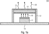
- Figure 1A shows a schematic side view of an emitter package 100 according to an embodiment
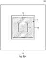
- Figure 1B shows a schematic top view of the emitter package 100.
- the emitter package 100 may comprise a MEMS infrared radiation source 11 for emitting pulsed infrared radiation 20 in a first wavelength range. Accordingly, the infrared radiation source 11 may also be referred to as a MEMS infrared emitter 11.
- the MEMS infrared emitter 11 may be configured to emit a broadband infrared signal 20.
- broadband infrared radiation may comprise wavelengths above 780 nm, e.g. between 780 nm and 1 mm, and preferably between 780 nm and 100 ⁇ m, or between 780 nm and 10 ⁇ m.
- the MEMS infrared radiation source 11 may be configured to emit infrared radiation 20 in the aforementioned wavelength ranges.
- the MEMS infrared radiation source 11 may be arranged on a substrate 10.
- the substrate 10 may be a laminate substrate, such as a Printed Circuit Board (PCB), for example.
- PCB Printed Circuit Board
- other types of substrates such as substrates comprising conducting materials, semiconducting materials or insulating materials, may be possible.
- the emitter package 100 may comprise a rigid wall structure 12 being arranged on the substrate 10.
- the rigid wall structure 12 may be arranged around the periphery of the MEMS infrared radiation source 11, or in other words, the rigid wall structure 12 may laterally surround the MEMS infrared radiation source 11.
- the rigid wall structure 12 may be in direct contact with or distanced from, i.e. not contacting, the MEMS infrared radiation source 11.
- the rigid wall structure 12 may be laterally and/or vertically distanced from the MEMS infrared radiation source 11.
- the rigid wall structure 12 may provide at least a laterally surrounding portion of the housing or package for housing or packaging the MEMS infrared radiation source 11.
- the vertical distance may be 1 mm or more, which will be explained in more detail somewhat later with reference to Figures 6 and 7 .
- the rigid wall structure 12 may be non-transparent or opaque (e.g. by at least 95% or more) with respect to the emitted infrared radiation 20 emitted by the MEMS infrared radiation source 11. Accordingly, the rigid wall structure 12 may substantially shield the emitted broadband infrared radiation 20 from radiating to the outside of the package.
- the rigid wall structure 12 may be arranged, e.g. mounted on the substrate 10 in a gapless manner, i.e. without any substantial gaps between the rigid wall structure 12 and the substrate 10 through which the emitted broadband infrared radiation 20 could otherwise escape. Therefore, an optional sealant may be provided at the transition between the rigid wall structure 12 and the substrate 10.
- the sealant may, for instance, be provided through an appropriate bonding means 53, e.g. an adhesive or glue (c.f. Figure 5G ).
- the emitter package 100 may further comprise a lid structure 13 being attached to the rigid wall structure 12.
- the lid structure 13 may comprise a filter structure 14 for filtering the broadband infrared radiation 20 emitted from the MEMS infrared radiation source 11 so as to provide a filtered infrared radiation 30 with a reduced second wavelength range.
- the filter structure 14 may be embedded in the lid structure 13, as exemplarily shown in Figure 1A .
- the filter structure 14 may be arranged on a bottom side of the lid structure 13, i.e. on a side of the lid structure 13 facing towards the MEMS infrared radiation source 11 (c.f. Figs. 2 and 6 ).
- the filter structure 14 may be arranged on a top side of the lid structure 13, i.e. on a side of the lid structure 13 facing away from the MEMS infrared radiation source 11.
- the MEMS infrared radiation source 11 may emit a broadband infrared radiation signal 20 in a first broadband wavelength range.
- the filter structure 14 may allow to transit only parts of the emitted broadband infrared radiation 20, i.e. filtered infrared radiation 30 in a reduced second wavelength range compared to the first broadband wavelength range.
- the filter structure 14 may only allow certain wavelengths to pass, which may be absorbed by an analyte that shall be detected.
- the filter structure 14 may only allow infrared radiation 30 at a wavelength of approximately ⁇ 4.2 ⁇ m to pass, since said wavelength corresponds to an absorption peak distinct to CO 2 molecules.
- the filter structure 14 may only allow a predetermined portion 30 of the emitted infrared radiation 20 to pass, said predetermined portion 30 comprising a predetermined wavelength with a tolerance of ⁇ 10% (e.g. ⁇ 4.2 ⁇ m ⁇ 10%), or a tolerance of 15%, or a tolerance of 20%.
- a tolerance of ⁇ 10% e.g. ⁇ 4.2 ⁇ m ⁇ 10%
- FIG. 2 shows a cross-sectional view of only a section of a lid structure 13 according to a non-limiting example (not drawn to scale).
- the lid structure 13 may comprise a lid substrate portion 13a, which may also be referred to as a die, for example bulk silicon,
- the lid substrate portion (die) 13a may comprise a thickness between 100 ⁇ m and 1000 ⁇ m, for example 650 ⁇ m as exemplarily depicted.
- the lid structure 13 may comprise a filter structure 14 that may be arranged at a first side (e.g. bottom side in Figure 2 ) of the lid substrate portion 13a, e.g. at a side of the lid substrate portion 13a or the lid structure 13 facing towards the MEMS infrared radiation source 11 in an assembled state.
- the filter structure 14 may comprise, or be provided as, a filter stack comprising two or more layers 21, 22 being alternatingly arranged atop each other.
- Figure 2 shows, as a non-limiting example, a first layer 21 comprising silicon oxide (SiO) and a second layer 22 comprising amorphous silicon (a-Si).
- SiO silicon oxide
- a-Si amorphous silicon
- other suitable materials may be possible.
- such an arrangement comprising a layer stack comprising a plurality of first layers 21 and a plurality of second layers 22 being alternatingly arranged one atop the other may be suitable as a gas filter stack for transiting only infrared radiation at a wavelength being suitable for detecting a particular gas.
- the filter structure 14 may be configured to transit only infrared radiation comprising a wavelength that is suitable for detecting a particular target gas.
- the filter structure 14 may be configured to transit only infrared radiation comprising a wavelength of approximately ⁇ 4.2 ⁇ m ⁇ 10%.
- the lid structure 13 may comprise an anti reflective coating (ARC) 15.
- the anti reflective coating 15 may be arranged at an opposite second side (e.g. top side in Figure 2 ) of the lid substrate portion 13a, i.e. opposite the filter structure 14, e.g. at a side of the lid structure 13 facing away from the MEMS infrared radiation source 11.
- the anti reflective coating 15 may comprise a layer stack comprising two or more layers 21, 22 being alternatingly arranged atop each other.
- Figure 2 shows, as a non-limiting example, a first layer 21 comprising silicon oxide (SiO) and a second layer 22 comprising amorphous silicon (a-Si).
- the anti reflective coating 15 may comprise a layer stack comprising a plurality of first layers 21 and a plurality of second layers 22 being alternatingly arranged one atop the other.
- the first and second layers 21, 22 in the filter stack 14 and/or in the anti reflective coating 15 may comprise the same or different materials, depending on the desired characteristics, for example the desired wavelengths to be filtered by the filter structure 14.
- a broadband infrared signal 20 being emitted from the MEMS infrared radiation source 11 may pass the lid structure 13, more particular the filter structure 14, the lid substrate portion 13a and the optionally available anti reflective coating 15.
- the filter structure 14 filters the broadband infrared signal 20 being emitted from the MEMS infrared radiation source 11 so as to produce the filtered infrared radiation 30 comprising a narrower second wavelength compared to the first broadband wavelength.
- the optionally available anti reflective coating 15 may increase the infrared signal throughput to about 90%.
- the lid structure 13 may comprise a filter stack 14 (e.g. suitable for CO 2 ) on the front side of the die 13a and an ARC (anti-reflective coating) 15 on the opposite back side of the die 13a.
- the filter stack 14 may only allow an infrared signal with a predetermined wavelength to transit, e.g. in case of CO 2 a wavelength of ⁇ 4.2 ⁇ m.
- said predetermined wavelength may correspond to an absorption peak distinct to molecules of an analyte, e.g. a target gas to be detected, such as CO 2 , for example.
- the lid structure 13 and the filter structure 14 may be configured such that the corresponding filter response may allow to pass wavelengths which are suitable to excite/detect other analytes (e.g. gases) different from CO 2 .
- these other analytes may comprise, for example, at least one of Methane, CO and volatile organic compounds (VOCs).
- the emitter package 100 may comprise a rigid wall structure 12 that shall be explained in more detail below with reference to Figures 3A to 3C .
- Figure 3A shows an example of a rigid wall structure 12 from a perspective view
- Figure 3B shows an assembled emitter package 100 comprising said rigid wall structure 12
- Figure 3C shows a cross-sectional side view of the assembled emitter package 100 comprising the rigid wall structure 12.
- the rigid wall structure 12 may comprise four adjacent wall portions 12a, 12b, 12c, 12d forming a rectangular, and particularly square-shaped, enclosure or cavity structure comprising a cavity portion 31 at the inside.
- the adjacent wall portions 12a, 12b, 12c, 12d may also be referred to as vertical or upright wall portions.
- the wall structure 12 may comprise a different number of adjacent wall portions 12a, 12b, 12c, 12c and/or a different geometrical shape than depicted.
- the rigid wall structure 12 may be topless and/or bottomless, i.e. the wall portions 12a, 12b, 12c, 12d may be freestanding or self-supporting.
- the rigid wall structure 12 may further comprise a bottom wall portion 12f that faces the substrate 10. Accordingly, the rigid wall structure 12 may be mounted onto the substrate 10 at its bottom wall portion 12f.
- the rigid wall structure 12 may further comprise a top wall portion 12e facing away from the substrate 10.
- the lid structure 13 may be arranged on said top wall portion 12e.
- the rigid wall structure 12 may be arranged on the substrate 10 at its bottom wall portion 12f and may laterally surround the MEMS infrared radiation source 11 that may also be arranged on the same substrate 10.
- the rigid wall structure 12 may be arranged around the periphery of the MEMS infrared radiation source 11. Accordingly, the MEMS infrared radiation source 11 may be placed inside the cavity 31 formed by the adjacent vertical wall portions 12a, 12b, 12c, 12d.
- the rigid wall structure 12 may comprise a height h, measured vertically from the substrate 10.
- the height h of the rigid wall structure 12 may be larger than a height of the MEMS infrared radiation source 11. Accordingly, in an assembled state, the rigid wall structure 12 may protrude from the substrate 10 to a greater extent than the mounted MEMS infrared radiation source 11.
- the lid structure 13 comprising the filter structure 14 may be mounted on a portion of the rigid wall structure 12 opposite the substrate 10, i.e. on the top wall portion 12e of the rigid wall structure 12 which faces away from the substrate 10. Accordingly, the rigid wall structure 12 and the thereon arranged lid structure 13 comprising the filter structure 14 may together provide the cavity 31 in which the MEMS infrared radiation source 11 is arranged.
- the lid structure 13 comprising the filter structure 14 may be bonded on top of the rigid wall structure 12 directly, i.e. on the plane surfaces of the top wall portion 12e (c.f. Figures 4C and 5F ).
- a recess structure may be provided on at least one of the top and the bottom side of the rigid wall structure 12.
- the rigid wall structure 12 may comprise a recess structure 33 being provided in the top wall portion 12e facing away from the substrate 10.
- the recess structure 33 may be arranged at the top of each of the adjacent vertical wall portions 12a, 12b, 12c, 12d.
- the recess structure 33 may be provided continuously along the top wall portion 12e of the adjacent wall portions 12a, 12b, 12c, 12d.
- the recess structure 33 may be provided along the lateral inner perimeter portion of the top wall portion 12e, which lateral inner perimeter portion faces the cavity 31.
- the lid structure 13 may then be placed inside said recess structure 33. Therefore, the outer lateral dimensions of the recess structure 33 may substantially correspond to the outer lateral dimensions of the lid structure 13 such that the lid structure 13 may fit into the recess structure 33, preferably without any substantial clearance.
- the rigid wall structure 12 may be opaque (e.g. to at least 95%) or non-transparent for the broadband infrared radiation 20 being emitted by the MEMS infrared radiation source 11.
- the lid structure 13 comprising the filter structure 14 may be at least partially transparent for the emitted infrared radiation 20 being emitted by the MEMS infrared radiation source 11. Accordingly, the rigid wall structure 12 and the lid structure 13 comprising the filter structure 14 may together provide the emitter package 100 which is laterally non-transparent for the emitted infrared radiation 20 except for the lid structure 13 being mounted on the top wall portion 12e which provides for an at least partly transmission of the emitted infrared radiation 20.
- Figure 3C shows an assembled emitter package 100 in a side sectional view.
- the MEMS infrared radiation source 11 is arranged inside the cavity 31 formed by the adjacent vertical wall portions 12a, 12b, 12c, 12d of the rigid wall structure 12. Accordingly, the adjacent vertical wall portions 12a, 12b, 12c, 12d may laterally surround the MEMS infrared radiation source 11 or, in other words, the adjacent vertical wall portions 12a, 12b, 12c, 12d may be arranged around the periphery of the MEMS infrared radiation source 11.
- the lid structure 13 comprising the filter structure 14 may be mounted on the top wall portion 12f, as explained above, e.g. at least partially inside the recess structure 33.
- the recess structure 33 may optionally comprise a standoff feature 34.
- This standoff feature 34, or standoff structure may be provided at a lateral inner perimeter portion of the recess structure 33 (i.e. an inner perimeter portion facing towards the cavity 31).
- the standoff feature 34 may be continuously provided at the lateral inner perimeter portion of the recess structure 33.
- the standoff structure 34 may stand off from a bottom 35 of the recess structure 33. That is, a distance d 1 between the top wall portion 12e and the standoff structure 34 is smaller than a distance d 2 between the top wall portion 12e and a bottom portion 35 of the recess structure 33.
- the standoff structure 34 is particularly useful for preventing a material used to bond the lid structure 13 to the wall structure 12, e.g. an adhesive, from flowing laterally inwards towards the MEMS infrared radiation source 11 inside the cavity 31 when mounting the lid structure 13.
- the additional optional recess structure 33 provided in the rigid wall structure 12 may be introduced to further improve the reliability of the emitter package 100.
- the recess structure 33 enables a good mechanical seal around the side of the lid structure 13 comprising the filter structure 14.
- the standoff feature 34 on the top wall portion 12e guarantees a desired bond line thickness of the lid/filter attach adhesive and stops the lid/filter attach adhesive from flowing into the cavity 31 towards the MEMS infrared radiation source 11.
- a standoff feature (not explicitly shown) similar to the one explained above, may be provided on the bottom wall portion 12f of the rigid wall structure 12. Such a standoff feature may guarantee the bond line thickness when attaching or bonding the rigid wall structure 12 onto the substrate 10.
- the emitter package 100 shall comprise a rigid wall structure 12 having a rigidity that is high enough to securely suspend the lid structure 13. Furthermore, the rigid wall structure shall not be prone to cracks. Still further, the rigid wall structure 12 shall be opaque or non-transparent to the emitted broadband infrared radiation 20 emitted by the MEMS infrared emitter 11. Yet further, the rigid wall structure 12 shall comprise a material that allows for an easy and secure attachment of the lid structure 13 as well as an easy and secure attachment of the wall structure 12 itself on the substrate 10. In order to fulfill all these requirements, the rigid wall structure 12 may comprise, or be made from, a Liquid Crystal Polymer (LCP).
- LCP Liquid Crystal Polymer
- LCP may be preferred since this will allow (besides the advantages already mentioned above) an emitter package 100 which has a considerably smaller footprint compared to conventional solutions.
- the footprint or the package outline dimensions of the emitter package 100 may, as a non-limiting example, be 4 ⁇ 4 ⁇ 2.3 mm (with ⁇ 0.1 mm tolerance).
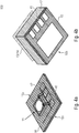
- Figures 4A-4C show an example of assembling such a small emitter package 100 according to the herein described innovative principle.
- Figure 4A shows the MEMS die 11 mounted onto the substrate 10.
- the substrate 10 may comprise a first (top) side 10a on which the MEMS infrared radiation source 11 is mounted, and an opposite second (bottom) side 10b.
- Figure 4A also shows wirebonds 42 connecting electrodes on the MEMS die surface to the substrate 10, e.g. to the first side 10a of the substrate 10.
- the substrate 10 may, for instance, be a laminate substrate, e.g. a PCB, having one or more electrical contacting regions 41.
- the MEMS infrared radiation source 11 may be connected to said electrical contacting regions 41 by means of bond wires 42, e.g. by gold wire bonds.
- this exemplary emitter package 100 may comprise a MEMS heater die or MEMS infrared radiation source 11, one or more gold wire bonds 42, a laminate substrate 10, a rigid wall structure 12, preferably comprising or being made from LCP, and a combined filter lid 13, 14, e.g. comprising or being made from silicon.
- Figure 4B shows a bottom view of the emitter package 100.
- the substrate 10 comprises the above mentioned one or more electrical contacting regions 41 on the bottom side 10b for attaching and contacting the emitter package 100 onto a carrier substrate, e.g. a system or component board (not shown).
- the (LCP) wall structure 12 may be bonded on the solder mask of the laminate substrate 10 at its top side 10a.
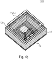
- Figure 4C shows a top view of the emitter package 100.
- the wall structure 12 may not comprise the above discussed recess structure 33.
- the top wall portion 12e of the rigid wall structure 12 may be substantially plane.
- the lid structure 13 comprising the filter structure 14 may be bonded directly onto said plane top wall portion 12e.
- the (silicon) filter lid structure 13, 14 may be bonded on top of the (LCP) wall structure 12 to create a sealed cavity 31, as explained above.
- the MEMS infrared radiation source 11 may emit a broadband IR signal 30 travelling towards the (silicon) filter lid structure 13, 14, the broadband IR signal 30 comprising a first broadband wavelength.
- the filter lid structure 13, 14 may only transit a portion of the broadband IR signal 20 having a reduced predetermined second wavelength, e.g. in the non-limiting example of CO 2 a wavelength of approximately ⁇ 4.2 ⁇ m.
- the filter structure 14 may be modified to selectively pass other wavelengths of light required to detect other gases.
- Figures 5A-5H show the single steps of an exemplary, and non-limiting, process of manufacturing and assembling an emitter package 100 according to the herein described innovative principle.
- the substrate 10 e.g. a laminate substrate such as a PCB or the like, may be provided.
- a bonding means 51 e.g. an adhesive, for bonding the MEMS infrared emitter 11 onto the substrate 10 may be provided at a predetermined portion on the first (top) side 10a of the substrate.
- the MEMS infrared emitter 11 may be bonded onto said predetermined portion of the substrate 10 comprising the bonding means 51.
- the MEMS infrared emitter 11 may be electrically contacted with dedicated electrical contacting regions 41 by means of electrical conductors, e.g. by means of bond wires 42.
- the rigid wall structure 12 may be provided.
- a bonding means 52 e.g. an adhesive, for bonding the lid structure 13 comprising the filter structure 14 may be provided at the top wall portion 12e of the rigid wall structure 12.
- the top wall portion 12e may be plane, as described above with reference to Figures 4A-4C .
- the top wall portion 12e may comprise the recess structure 33 (and optionally the standoff structure 34) as described above with reference to Figures 3A-3C .
- the bonding means 52 would be provided inside the recess structure 33.
- the lid structure 13 comprising the filter structure 14 may be bonded onto the top wall portion 12e by means of the bonding means 52.
- a bonding means 53 may be provided along lateral outer perimeter portions at the first (top) side 10a of the substrate 10 for bonding the rigid wall structure 12 with the substrate 10.
- the rigid wall structure 12 having the lid/filter structure 13, 14 arranged thereon may be bonded with the substrate 10 by means of suitable bonding means 53, e.g. an adhesive or glue, being provided on the lateral outer perimeter portions of the substrate 10.
- suitable bonding means 53 e.g. an adhesive or glue
- the bottom wall portion 12f of the rigid wall structure 12 may be attached to the bonding means 53 arranged on the first (top) side 10a of the substrate 10.
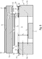
- Figure 6 shows a further example of an emitter package 100 according to the herein described innovative principle. It shows one non-limiting example of how the lid structure 13 comprising the filter structure 14 may be bonded with the rigid wall structure 12.
- the lid structure 13 may comprise a lid substrate 13a, e.g. a bulk silicon. Silicon may comprise a good bonding capability with LCP, in case the rigid wall structure 12 comprises, or is made from, LCP. However, additionally or alternatively, the lid substrate 13a may comprise other materials than silicon which may also have a good bonding capability with LCP.
- a lid substrate 13a e.g. a bulk silicon. Silicon may comprise a good bonding capability with LCP, in case the rigid wall structure 12 comprises, or is made from, LCP.
- the lid substrate 13a may comprise other materials than silicon which may also have a good bonding capability with LCP.
- the filter structure 14 may be arranged on the lid substrate 13a, e.g. on a first side (e.g. front side) facing towards the MEMS infrared emitter 11.
- the optional anti reflective coating ARC 15 may be arranged on the other side (e.g. back side) of the lid substrate 13a, e.g. on an opposite second side facing away from the MEMS infrared emitter 11.
- the front side of the lid structure 13 (e.g. with CO 2 filter stack 14) may be bonded directly on the plane surfaces of the top wall portion 12e of the rigid wall structure 12, as shown in Figure 6 .
- the front side of the lid structure 13 e.g. with CO 2 filter stack 14
- the lid structure 13 may be bonded directly on the plane surfaces of the top wall portion 12e of the rigid wall structure 12, as shown in Figure 6 .
- everything that is described herein with reference to the embodiment of Figure 6 also holds true for a rigid wall structure 12 having the optional recess structure 33, as discussed above with reference to Figures 3A to 3C .
- the anti reflective coating 15 may be structured, e.g. by means of etching.
- the anti reflective coating 15 may comprise a predetermined marking 57, e.g. a "Pin 1" marking, to assist pattern recognition in the package assembly and test. This avoids use of an expensive laser marking machine which is capable of marking on silicon.
- the anti reflective coating 15 may comprise an indication for marking a predetermined pin connecting point.
- lateral outer perimeter portions of the anti reflective coating 15 may be etched away along the lateral outer edges of the lid substrate 13a, such that said lateral outer edges of the lid substrate 13a may remain uncovered. This may provide for a dicing street 56.
- the filter structure 14 may be structured, e.g. by means of etching.
- the filter structure 14 may be etched away such that these lateral outer perimeter portions of the lid substrate 13a remain uncovered.
- the lid substrate 13a may comprise one or more uncovered portions 55 facing the top wall portion 12e.
- the uncovered portion 55 may, for example, be arranged along the lateral outer edges of the lid substrate 13a, i.e. the filter structure 14 may be completely removed along the entire lateral outer perimeter of the first side of the lid substrate 13a that faces towards the MEMS infrared emitter 11.
- the filter structure 14 may at least partially cover the first side of the lid substrate 13a leaving a lateral outer perimeter portion 55 of the lid structure 13 uncovered, wherein the lid structure 13 may be attached to the rigid wall structure 12 at least at said uncovered lateral outer perimeter portion 55.
- the filter structure 14 may laterally overlap, at least partially, with the top wall portion 12e and the bonding means 52 arranged thereon.
- This is indicated in Figure 6 as an overlapping portion 58 comprising a lateral overlap O 1 .
- Said lateral overlap O 1 may range from 20 ⁇ m to 200 ⁇ m, or from 50 ⁇ m to 150 ⁇ m.
- the lateral overlap O 1 may be 100 ⁇ m ⁇ 10%.
- the overlapping portion 58 may comprise a lateral extension O 1 of 100 ⁇ m or less at which the filter structure 14 laterally overlaps with the rigid wall structure 12.
- a lateral overlap O 1 of 100 ⁇ m or less between the lid/filter structure 13, 14 and the adhesion area 52 may allow a desired placement tolerance in the assembly process.
- the lid structure 13 may comprise an overlapping portion 58 at which the filter structure 14 may laterally overlap with the rigid wall structure 12, wherein the lid structure 13 may be attached to the rigid wall structure 12 with at least one of its uncovered portion 55 and its overlapping portion 58. In some embodiments, the lid structure 13 may be attached to the rigid wall structure 12 with both its uncovered portion 55 and its overlapping portion 58.
- a bonding means 52 e.g. an adhesive or glue, may be provided at the top wall portion 12e of the rigid wall structure 12.
- the bonding means 52 may comprise a bond line thickness BLT ranging between 10 ⁇ m and 50 ⁇ m, or between 20 ⁇ m and 40 ⁇ m. In some non-limiting examples the BLT may be approximately 30 ⁇ m ⁇ 10%.
- the lid structure 13 may then be attached to the rigid wall structure 12 by means of said bonding means 52.
- the above mentioned uncovered portions 55 of the lid substrate 13a may be brought into contact with the bonding means 52.
- the lid structure 13 may be provided as a double-side etched die, e.g. comprising or being made from silicon.
- a double-side etched die e.g. comprising or being made from silicon.
- those portions of the filter structure 14 which directly face the adhesion area i.e. the bonding means 52 may be etched away to improve the adhesion with the wall structure 12.
- this non-limiting exemplary embodiment may provide for a reduced size of the overlapping regions 55 providing an improved filter placement accuracy.
- each of the adjacent vertical side wall portions 12a-12d of the rigid wall structure 12 may comprise a lateral thickness D 1 ranging between 0.1 mm and 1.0 mm, or between 0.25 mm and 0.75 mm.
- the lateral thickness D 1 may be 0.5 mm ⁇ 10%.
- the cavity 31 that is formed by the adjacent vertical side wall portions 12a-12d of the rigid wall structure 12 may comprise a lateral inner dimension D 2 ranging between 1 mm and 5 mm, or between 2 mm and 4 mm. In some non-limiting examples, the lateral inner dimension D 2 may be 3 mm ⁇ 10%.
- a predetermined minimum vertical distance H 1 between the MEMS infrared emitter 11 and the lid structure 13 or filter structure 14 can be securely provided.
- the rigid wall structure 12 may comprise, or may be made from, LCP. This may be advantageous since it allows to provide a package or housing (i.e. the rigid wall structure 12) having rigid side wall portions 12a-12d.
- the rigidity of said side wall portions 12a-12d is sufficiently strong so as to provide a self-supporting wall structure 12 or package at which the lid structure 13 comprising the filter structure 14 may be securely attached.
- said predetermined minimum vertical distance H 1 is 1 mm or more.
- a requirement of a PAS sensor foresees a minimum distance between the infrared emitter 11 and the lid structure 13 of at least 1 mm.
- a deep cavity of at least 1 mm has to be created by patterning and joining together individual ceramic sheets.
- the tooling cost of such a ceramic package with deep cavity is too high to fulfil the cost requirement of the entire sensor solution.
- QFN molded packages may be provided.
- QFN packages may tend to crack at the interface between lead frame and mold compound.
- the herein described innovative principle suggests a rigid wall structure 12 comprising, or being made from, a Liquid Crystal Polymer (LCP).
- LCP Liquid Crystal Polymer
- the LCP wall structure 12 may provide a rigid structure that is rigid enough to suspend the lid structure 13 spaced apart from the MEMS infrared emitter 11 at a vertical distance H 1 of at least 1 mm.
- the tooling costs for the innovative LCP wall structure 12 are considerably lower compared to conventional packages.
- the LCP wall structure 12 may be easily mounted on the substrate 10, e.g. by appropriate bonding means 53, such as adhesives or glues.
- certain embodiments may provide a photo acoustic emitter package 100 constructed using a liquid crystal polymer (LCP) wall structure 12 and sealed by a double-side etched lid structure 13.
- LCP liquid crystal polymer
- this disclosure describes an LCP (liquid crystal polymer) sidewall structure 12 in combination with a double-side etched (silicon) filter lid 13, 14.
- the LCP material fulfils the requirement of a rigid sidewall structure 12 that also blocks the unfiltered IR signal 30.
- the LCP package also has low set up/tooling costs.
- FIG. 7 shows a non-limiting example of a photoacoustic sensor 1000 according to an embodiment.
- the photoacoustic sensor 1000 may comprise an emitter package 100 according to the innovative principle as described herein.
- the emitter package 100 may be arranged on a substrate 110.
- the photoacoustic sensor 1000 may further comprise a pressure transducer 1020, e.g. a microphone, being arranged on the same substrate 110 next to the emitter package 100.
- the photoacoustic sensor 1000 may further comprise a housing 1010, e.g. a non-transparent metal lid being soldered onto the substrate 110.
- the housing 1010 may define a measurement chamber 1030.
- the emitter package 100 and the pressure transducer 1020 may be arranged inside said measurement chamber 1030.
- the emitter package 100 may emit into the measurement chamber 1030 the filtered infrared radiation 30 at the reduced second wavelength after passing the lid structure 13 comprising the filter structure 14.
- the filter structure 14 may be configured to let infrared radiation pass having a reduced second wavelength of approximately ⁇ 4.2 ⁇ m ⁇ 10%.
- the CO 2 molecules may absorb the emitted (pulsed) infrared radiation 30, which molecules begin to alternatingly heating up and cooling down thereby creating pressure or sound waves inside the measurement chamber 1030 which can be detected by the pressure transducer 1020.
- the exemplarily depicted photoacoustic gas sensor 1000 comprises the herein described innovative emitter package 100 comprising a MEMS die 11 that emits a pulsed broadband infrared (IR) signal 20.
- the emitter package 100 may generate a filtered pulsed infrared signal 30 with a reduced wavelength, e.g. a wavelength of ⁇ 4.2 ⁇ m ⁇ 10%, which is absorbed by particular gas molecules, e.g. by CO 2 gas molecules.
- the absorbed energy causes local heating and a pressure change in the gas sensor 1000 that can be detected by, e.g. a silicon microphone 1020.
- the signal generated by the microphone 1020 correlates with the CO 2 concentration in the ambient air.
- the emitter package 100 may comprise:
- an emitter package 100 with an LCP sidewall structure 12 enables a new cost-sensitive, optical package 100 concept for gas sensors 1000.
- the double-side etched (silicon) filter lid structure 13, 14 improves the package reliability with minimum disturbance in the assembly operation.
- Use of the LCP sidewall structure 12 may also enable a smaller footprint compared to a conventional molded cavity solution.
- the use of the MEMS infrared emitter 11 within the emitter package 100 may enable a fast responding infra-red light source.
- the herein described emitter package 100 may enable a considerable miniaturization gas sensors 1000, such as CO 2 sensors, for example.
- the herein described photoacoustic sensor 1000 is ideal for smart home applications and building automation as well as indoor air quality loT devices.
- the gas sensor 1000 as described herein saves more than 75% of space in customer end products compared to commercially available gas sensors.
- the disclosure also enables unprecedented low manufacturing costs compared to solutions containing LEDs and lasers, which are commonly used as mid-infrared light sources for photoacoustic systems.
- the gas sensor 1000 as described herein may not only enable high volume and cost sensitive CO 2 gas sensing applications, but it may also allow for sensing other gases and volatile organic compounds.
- an emitter package 100 for a photoacoustic sensor 1000 comprising:
- the step of arranging the MEMS infrared radiation source 11 on the substrate 10 may be executed prior to the step of arranging the wall structure 12 on the substrate 10.
- the rigid wall structure 12 may laterally surround the MEMS infrared radiation source 11. Accordingly, the rigid wall structure 12 may form a cavity 31 inside of which the MEMS infrared radiation source 11 resides. Providing such a cavity 31 enables a smaller solution since no additional space inside the cavity 31 is required to accommodate the bond head.
- aspects have been described in the context of an apparatus, it is clear that these aspects also represent a description of the corresponding method, where a block or device corresponds to a method step or a feature of a method step. Analogously, aspects described in the context of a method step also represent a description of a corresponding block or item or feature of a corresponding apparatus.
Landscapes
- Engineering & Computer Science (AREA)
- Microelectronics & Electronic Packaging (AREA)
- Physics & Mathematics (AREA)
- General Physics & Mathematics (AREA)
- Computer Hardware Design (AREA)
- Chemical & Material Sciences (AREA)
- Analytical Chemistry (AREA)
- Health & Medical Sciences (AREA)
- General Health & Medical Sciences (AREA)
- Life Sciences & Earth Sciences (AREA)
- Biochemistry (AREA)
- Immunology (AREA)
- Pathology (AREA)
- Spectroscopy & Molecular Physics (AREA)
- Manufacturing & Machinery (AREA)
- Acoustics & Sound (AREA)
- Radar, Positioning & Navigation (AREA)
- Remote Sensing (AREA)
- Toxicology (AREA)
- Micromachines (AREA)
- Investigating Or Analysing Materials By Optical Means (AREA)
- Photometry And Measurement Of Optical Pulse Characteristics (AREA)
Abstract
Description
- Embodiments of the present disclosure relate to a package comprising an emitter device for a photoacoustic sensor. Some particular but non-limiting examples refer to an emitter package comprising a rigid wall structure and a lid structure being attached to the wall structure. In some embodiments, the lid structure may comprise an integrated filter structure.
- The photo acoustic (PA) effect is based on the transformation of pulsed radiation energy into sound. Photo acoustic spectroscopy (PAS) concepts may be used for detecting different gases based on the photoacoustic effect. Pulsed radiation (e.g. infrared: IR) may be emitted into a measurement chamber comprising a gas or a mixture of gases containing at least one analyte, i.e. at least one gas to be detected, such as CO2, for example. The gas may absorb the energy of the emitted pulsed radiation which causes an alternating local heating of the gas, which leads to a thermal expansion inside the measurement chamber creating a pressure wave that may be detected as sound. Certain gases may absorb the energy at different wavelengths creating a characteristic pressure wave or sound profile.
- In photo acoustic spectroscopy, hermetically sealed packages, e.g. ceramic packages and metal can packages, can be used to offer a rigid package architecture and high reliability with minimum infrared signal leakage over the lifetime of the application. Some photoacoustic sensors may comprise a MEMS membrane as an infrared heat source and a lid being transparent for the emitted radiation. Known PAS emitter packages require a deep cavity with a minimum distance of 1 mm between the MEMS membrane to the lid. The tooling costs of a ceramic package with such a deep cavity is, however, too high to fulfil the cost requirement of an entire gas sensor solution. Regarding metal can packages, these are typically high cost due to the materials and processes used in their manufacture. However, the costs of such a gas sensor solution will not be competitive if an expensive metal can, e.g. with sapphire glass window, is used.
- Molded QFN packages (Quad Flat No-lead package) offer a cavity solution with a reasonable cost. However, there is a potential reliability issue due to cracking at the interface between leadframe and mold compound. Broadband unfiltered IR signal may leak through the crack. In addition, wire bonding into a pre-moulded cavity requires space between the emitter die and cavity side wall in order to accommodate the wire bonding head. This space is required to prevent the head from coming into contact with the walls of the cavity during wire bonding and results in a larger package footprint. Furthermore, conventional solutions for monitoring gases, such as the odourless and colourless CO2, are bulky and costly or simply not good enough for a widespread adoption.
- Thus, it is desired to provide a photoacoustic sensor and an emitter package for a photoacoustic sensor, in which the emitter package is small, robust, reliable and at the same time producible at low cost.
- Therefore, it is suggested to provide an emitter package for a photoacoustic sensor comprising the features of independent claim 1.
- According to an aspect of the present disclosure, the emitter package may comprise a MEMS infrared radiation source for emitting pulsed infrared radiation in a first wavelength range. The MEMS infrared radiation source may be arranged on a substrate. The emitter package may further comprise a rigid wall structure being arranged on the substrate. The rigid wall structure may laterally surround a periphery of the MEMS infrared radiation source. The emitter package may further comprise a lid structure being attached to the wall structure. The lid structure may comprise a filter structure for filtering the infrared radiation emitted from the MEMS infrared radiation source thereby providing a filtered infrared radiation in a reduced second wavelength range.
- Some non-limiting examples, variations and embodiments are defined in the dependent claims.
- In the following, embodiments of the present disclosure are described in more detail with reference to the figures, in which:
- Fig. 1A
- shows a schematic block diagram of a side cross-sectional view of an emitter package according to an embodiment,
- Fig. 1B
- shows a schematic top view of an emitter package according to an embodiment,
- Fig. 2
- shows a schematic cross-sectional side view of a section of a lid structure comprising a filter structure and an optional anti reflective coating according to an embodiment,
- Fig. 3A
- shows a schematic perspective view of a rigid wall structure according to an embodiment,
- Fig. 3B
- shows a perspective view of an emitter package according to an embodiment,
- Fig. 3C
- shows a schematic cross-sectional view of an emitter package according to an embodiment,
- Fig. 4A
- shows a schematic perspective top view of a MEMS infrared emitter mounted on a substrate,
- Fig. 4B
- shows a perspective bottom view of an emitter package according to an embodiment,
- Fig. 4C
- shows a perspective top view of an emitter package according to an embodiment,
- Figs. 5A-5H
- show a method of assembling an emitter package according to an embodiment,
- Fig. 6
- shows a schematic cross-sectional view of an emitter package according to an embodiment before the lid structure is mounted onto the rigid wall structure, and
- Fig. 7
- shows a schematic side view of a photoacoustic sensor according to an embodiment.
- Equal or equivalent elements or elements with equal or equivalent functionality are denoted in the following description by equal or equivalent reference numerals.
- Method steps which are depicted by means of a block diagram and which are described with reference to said block diagram may also be executed in an order different from the depicted and/or described order. Furthermore, method steps concerning a particular feature of a device may be replaceable with said feature of said device, and the other way around.
-
Figure 1A shows a schematic side view of anemitter package 100 according to an embodiment, andFigure 1B shows a schematic top view of theemitter package 100. - The
emitter package 100 may comprise a MEMSinfrared radiation source 11 for emitting pulsedinfrared radiation 20 in a first wavelength range. Accordingly, theinfrared radiation source 11 may also be referred to as a MEMSinfrared emitter 11. The MEMSinfrared emitter 11 may be configured to emit a broadbandinfrared signal 20. - In this disclosure, broadband infrared radiation may comprise wavelengths above 780 nm, e.g. between 780 nm and 1 mm, and preferably between 780 nm and 100 µm, or between 780 nm and 10 µm. The MEMS
infrared radiation source 11 may be configured to emitinfrared radiation 20 in the aforementioned wavelength ranges. - The MEMS
infrared radiation source 11 may be arranged on asubstrate 10. Thesubstrate 10 may be a laminate substrate, such as a Printed Circuit Board (PCB), for example. However, other types of substrates, such as substrates comprising conducting materials, semiconducting materials or insulating materials, may be possible. - The
emitter package 100 may comprise arigid wall structure 12 being arranged on thesubstrate 10. Therigid wall structure 12 may be arranged around the periphery of the MEMSinfrared radiation source 11, or in other words, therigid wall structure 12 may laterally surround the MEMSinfrared radiation source 11. Therigid wall structure 12 may be in direct contact with or distanced from, i.e. not contacting, the MEMSinfrared radiation source 11. For example, as shown inFigure 1A , therigid wall structure 12 may be laterally and/or vertically distanced from the MEMSinfrared radiation source 11. - Accordingly, the
rigid wall structure 12 may provide at least a laterally surrounding portion of the housing or package for housing or packaging the MEMSinfrared radiation source 11. The vertical distance may be 1 mm or more, which will be explained in more detail somewhat later with reference toFigures 6 and7 . - The
rigid wall structure 12 may be non-transparent or opaque (e.g. by at least 95% or more) with respect to the emittedinfrared radiation 20 emitted by the MEMSinfrared radiation source 11. Accordingly, therigid wall structure 12 may substantially shield the emitted broadbandinfrared radiation 20 from radiating to the outside of the package. Therigid wall structure 12 may be arranged, e.g. mounted on thesubstrate 10 in a gapless manner, i.e. without any substantial gaps between therigid wall structure 12 and thesubstrate 10 through which the emitted broadbandinfrared radiation 20 could otherwise escape. Therefore, an optional sealant may be provided at the transition between therigid wall structure 12 and thesubstrate 10. The sealant may, for instance, be provided through an appropriate bonding means 53, e.g. an adhesive or glue (c.f.Figure 5G ). - The
emitter package 100 may further comprise alid structure 13 being attached to therigid wall structure 12. Thelid structure 13 may comprise afilter structure 14 for filtering the broadbandinfrared radiation 20 emitted from the MEMSinfrared radiation source 11 so as to provide a filteredinfrared radiation 30 with a reduced second wavelength range. - The
filter structure 14 may be embedded in thelid structure 13, as exemplarily shown inFigure 1A . Alternatively, thefilter structure 14 may be arranged on a bottom side of thelid structure 13, i.e. on a side of thelid structure 13 facing towards the MEMS infrared radiation source 11 (c.f.Figs. 2 and6 ). Further alternatively, thefilter structure 14 may be arranged on a top side of thelid structure 13, i.e. on a side of thelid structure 13 facing away from the MEMSinfrared radiation source 11. - As mentioned above, the MEMS
infrared radiation source 11 may emit a broadbandinfrared radiation signal 20 in a first broadband wavelength range. Thefilter structure 14 may allow to transit only parts of the emitted broadbandinfrared radiation 20, i.e. filteredinfrared radiation 30 in a reduced second wavelength range compared to the first broadband wavelength range. For instance, thefilter structure 14 may only allow certain wavelengths to pass, which may be absorbed by an analyte that shall be detected. For example, if CO2 shall be detected, thefilter structure 14 may only allowinfrared radiation 30 at a wavelength of approximately ∼ 4.2 µm to pass, since said wavelength corresponds to an absorption peak distinct to CO2 molecules. Thus, in more general terms, thefilter structure 14 may only allow apredetermined portion 30 of the emittedinfrared radiation 20 to pass, saidpredetermined portion 30 comprising a predetermined wavelength with a tolerance of ±10% (e.g. ∼ 4.2 µm ±10%), or a tolerance of 15%, or a tolerance of 20%. -
Figure 2 shows a cross-sectional view of only a section of alid structure 13 according to a non-limiting example (not drawn to scale). Thelid structure 13 may comprise alid substrate portion 13a, which may also be referred to as a die, for example bulk silicon, The lid substrate portion (die) 13a may comprise a thickness between 100 µm and 1000 µm, for example 650 µm as exemplarily depicted. Thelid structure 13 may comprise afilter structure 14 that may be arranged at a first side (e.g. bottom side inFigure 2 ) of thelid substrate portion 13a, e.g. at a side of thelid substrate portion 13a or thelid structure 13 facing towards the MEMSinfrared radiation source 11 in an assembled state. - The
filter structure 14 may comprise, or be provided as, a filter stack comprising two ormore layers Figure 2 shows, as a non-limiting example, afirst layer 21 comprising silicon oxide (SiO) and asecond layer 22 comprising amorphous silicon (a-Si). Of course, other suitable materials may be possible. However, such an arrangement comprising a layer stack comprising a plurality offirst layers 21 and a plurality ofsecond layers 22 being alternatingly arranged one atop the other may be suitable as a gas filter stack for transiting only infrared radiation at a wavelength being suitable for detecting a particular gas. In other words, thefilter structure 14 may be configured to transit only infrared radiation comprising a wavelength that is suitable for detecting a particular target gas. In the non-limiting case of CO2, e.g. thefilter structure 14 may be configured to transit only infrared radiation comprising a wavelength of approximately ∼ 4.2 µm ±10%. - Optionally, the
lid structure 13 may comprise an anti reflective coating (ARC) 15. The antireflective coating 15 may be arranged at an opposite second side (e.g. top side inFigure 2 ) of thelid substrate portion 13a, i.e. opposite thefilter structure 14, e.g. at a side of thelid structure 13 facing away from the MEMSinfrared radiation source 11. Similar to the above describedfilter structure 14, the antireflective coating 15 may comprise a layer stack comprising two ormore layers Figure 2 shows, as a non-limiting example, afirst layer 21 comprising silicon oxide (SiO) and asecond layer 22 comprising amorphous silicon (a-Si). Of course, other suitable materials may be possible. Accordingly, the antireflective coating 15 may comprise a layer stack comprising a plurality offirst layers 21 and a plurality ofsecond layers 22 being alternatingly arranged one atop the other. - The first and
second layers filter stack 14 and/or in the antireflective coating 15 may comprise the same or different materials, depending on the desired characteristics, for example the desired wavelengths to be filtered by thefilter structure 14. - Accordingly, a broadband
infrared signal 20 being emitted from the MEMSinfrared radiation source 11 may pass thelid structure 13, more particular thefilter structure 14, thelid substrate portion 13a and the optionally available antireflective coating 15. Thefilter structure 14 filters the broadbandinfrared signal 20 being emitted from the MEMSinfrared radiation source 11 so as to produce the filteredinfrared radiation 30 comprising a narrower second wavelength compared to the first broadband wavelength. The optionally available antireflective coating 15 may increase the infrared signal throughput to about 90%. - Summarizing, the lid structure 13 (e.g. comprising silicon) may comprise a filter stack 14 (e.g. suitable for CO2) on the front side of the
die 13a and an ARC (anti-reflective coating) 15 on the opposite back side of thedie 13a. Thefilter stack 14 may only allow an infrared signal with a predetermined wavelength to transit, e.g. in case of CO2 a wavelength of ∼ 4.2 µm. Generally, said predetermined wavelength may correspond to an absorption peak distinct to molecules of an analyte, e.g. a target gas to be detected, such as CO2, for example. - Of course, CO2 is only mentioned herein as a non-limiting example. The
lid structure 13 and thefilter structure 14 may be configured such that the corresponding filter response may allow to pass wavelengths which are suitable to excite/detect other analytes (e.g. gases) different from CO2. These other analytes may comprise, for example, at least one of Methane, CO and volatile organic compounds (VOCs). - As mentioned above, the
emitter package 100 may comprise arigid wall structure 12 that shall be explained in more detail below with reference toFigures 3A to 3C .Figure 3A shows an example of arigid wall structure 12 from a perspective view,Figure 3B shows an assembledemitter package 100 comprising saidrigid wall structure 12, andFigure 3C shows a cross-sectional side view of the assembledemitter package 100 comprising therigid wall structure 12. - The
rigid wall structure 12 may comprise fouradjacent wall portions cavity portion 31 at the inside. Theadjacent wall portions wall structure 12 may comprise a different number ofadjacent wall portions rigid wall structure 12 may be topless and/or bottomless, i.e. thewall portions - The
rigid wall structure 12 may further comprise abottom wall portion 12f that faces thesubstrate 10. Accordingly, therigid wall structure 12 may be mounted onto thesubstrate 10 at itsbottom wall portion 12f. Therigid wall structure 12 may further comprise atop wall portion 12e facing away from thesubstrate 10. Thelid structure 13 may be arranged on saidtop wall portion 12e. - As can be seen in
Figure 3B , therigid wall structure 12 may be arranged on thesubstrate 10 at itsbottom wall portion 12f and may laterally surround the MEMSinfrared radiation source 11 that may also be arranged on thesame substrate 10. In other words, therigid wall structure 12 may be arranged around the periphery of the MEMSinfrared radiation source 11. Accordingly, the MEMSinfrared radiation source 11 may be placed inside thecavity 31 formed by the adjacentvertical wall portions - The
rigid wall structure 12 may comprise a height h, measured vertically from thesubstrate 10. The height h of therigid wall structure 12 may be larger than a height of the MEMSinfrared radiation source 11. Accordingly, in an assembled state, therigid wall structure 12 may protrude from thesubstrate 10 to a greater extent than the mounted MEMSinfrared radiation source 11. - The
lid structure 13 comprising thefilter structure 14 may be mounted on a portion of therigid wall structure 12 opposite thesubstrate 10, i.e. on thetop wall portion 12e of therigid wall structure 12 which faces away from thesubstrate 10. Accordingly, therigid wall structure 12 and the thereon arrangedlid structure 13 comprising thefilter structure 14 may together provide thecavity 31 in which the MEMSinfrared radiation source 11 is arranged. - In an assembly process of the
emitter package 100, thelid structure 13 comprising the filter structure 14 (e.g. with CO2 filter stack) may be bonded on top of therigid wall structure 12 directly, i.e. on the plane surfaces of thetop wall portion 12e (c.f.Figures 4C and5F ). In order to guarantee a bond line thickness at the interface between thelid structure 13 and therigid wall structure 12, and/or between therigid wall structure 12 and thesubstrate 10, a recess structure may be provided on at least one of the top and the bottom side of therigid wall structure 12. - In the depicted non-limiting example of
Figure 3A , therigid wall structure 12 may comprise arecess structure 33 being provided in thetop wall portion 12e facing away from thesubstrate 10. Therecess structure 33 may be arranged at the top of each of the adjacentvertical wall portions recess structure 33 may be provided continuously along thetop wall portion 12e of theadjacent wall portions Figure 3A by way of a non-limiting example, therecess structure 33 may be provided along the lateral inner perimeter portion of thetop wall portion 12e, which lateral inner perimeter portion faces thecavity 31. As can be seen inFigure 3B , thelid structure 13 may then be placed inside saidrecess structure 33. Therefore, the outer lateral dimensions of therecess structure 33 may substantially correspond to the outer lateral dimensions of thelid structure 13 such that thelid structure 13 may fit into therecess structure 33, preferably without any substantial clearance. - As mentioned above, the
rigid wall structure 12 may be opaque (e.g. to at least 95%) or non-transparent for the broadbandinfrared radiation 20 being emitted by the MEMSinfrared radiation source 11. However, as mentioned above, thelid structure 13 comprising thefilter structure 14 may be at least partially transparent for the emittedinfrared radiation 20 being emitted by the MEMSinfrared radiation source 11. Accordingly, therigid wall structure 12 and thelid structure 13 comprising thefilter structure 14 may together provide theemitter package 100 which is laterally non-transparent for the emittedinfrared radiation 20 except for thelid structure 13 being mounted on thetop wall portion 12e which provides for an at least partly transmission of the emittedinfrared radiation 20. -
Figure 3C shows an assembledemitter package 100 in a side sectional view. The MEMSinfrared radiation source 11 is arranged inside thecavity 31 formed by the adjacentvertical wall portions rigid wall structure 12. Accordingly, the adjacentvertical wall portions infrared radiation source 11 or, in other words, the adjacentvertical wall portions infrared radiation source 11. Thelid structure 13 comprising thefilter structure 14 may be mounted on thetop wall portion 12f, as explained above, e.g. at least partially inside therecess structure 33. - As can be seen in detail here, the
recess structure 33 may optionally comprise astandoff feature 34. Thisstandoff feature 34, or standoff structure, may be provided at a lateral inner perimeter portion of the recess structure 33 (i.e. an inner perimeter portion facing towards the cavity 31). For example, thestandoff feature 34 may be continuously provided at the lateral inner perimeter portion of therecess structure 33. Thestandoff structure 34 may stand off from a bottom 35 of therecess structure 33. That is, a distance d1 between thetop wall portion 12e and thestandoff structure 34 is smaller than a distance d2 between thetop wall portion 12e and abottom portion 35 of therecess structure 33. Thestandoff structure 34 is particularly useful for preventing a material used to bond thelid structure 13 to thewall structure 12, e.g. an adhesive, from flowing laterally inwards towards the MEMSinfrared radiation source 11 inside thecavity 31 when mounting thelid structure 13. - The additional
optional recess structure 33 provided in therigid wall structure 12 may be introduced to further improve the reliability of theemitter package 100. Therecess structure 33 enables a good mechanical seal around the side of thelid structure 13 comprising thefilter structure 14. Thestandoff feature 34 on thetop wall portion 12e guarantees a desired bond line thickness of the lid/filter attach adhesive and stops the lid/filter attach adhesive from flowing into thecavity 31 towards the MEMSinfrared radiation source 11. - Additionally or alternatively, a standoff feature (not explicitly shown) similar to the one explained above, may be provided on the
bottom wall portion 12f of therigid wall structure 12. Such a standoff feature may guarantee the bond line thickness when attaching or bonding therigid wall structure 12 onto thesubstrate 10. - Summarizing, the
emitter package 100 shall comprise arigid wall structure 12 having a rigidity that is high enough to securely suspend thelid structure 13. Furthermore, the rigid wall structure shall not be prone to cracks. Still further, therigid wall structure 12 shall be opaque or non-transparent to the emitted broadbandinfrared radiation 20 emitted by the MEMSinfrared emitter 11. Yet further, therigid wall structure 12 shall comprise a material that allows for an easy and secure attachment of thelid structure 13 as well as an easy and secure attachment of thewall structure 12 itself on thesubstrate 10. In order to fulfill all these requirements, therigid wall structure 12 may comprise, or be made from, a Liquid Crystal Polymer (LCP). - Even though other mold compounds, which have similar mechanical and optical performance compared to LCP, may be used, LCP may be preferred since this will allow (besides the advantages already mentioned above) an
emitter package 100 which has a considerably smaller footprint compared to conventional solutions. The footprint or the package outline dimensions of theemitter package 100 may, as a non-limiting example, be 4 × 4 × 2.3 mm (with ±0.1 mm tolerance). -
Figures 4A-4C show an example of assembling such asmall emitter package 100 according to the herein described innovative principle.Figure 4A shows the MEMS die 11 mounted onto thesubstrate 10. Thesubstrate 10 may comprise a first (top)side 10a on which the MEMSinfrared radiation source 11 is mounted, and an opposite second (bottom)side 10b.Figure 4A also shows wirebonds 42 connecting electrodes on the MEMS die surface to thesubstrate 10, e.g. to thefirst side 10a of thesubstrate 10. - The
substrate 10 may, for instance, be a laminate substrate, e.g. a PCB, having one or more electrical contactingregions 41. The MEMSinfrared radiation source 11 may be connected to said electrical contactingregions 41 by means ofbond wires 42, e.g. by gold wire bonds. Accordingly, thisexemplary emitter package 100 may comprise a MEMS heater die or MEMSinfrared radiation source 11, one or moregold wire bonds 42, alaminate substrate 10, arigid wall structure 12, preferably comprising or being made from LCP, and a combinedfilter lid -
Figure 4B shows a bottom view of theemitter package 100. Thesubstrate 10 comprises the above mentioned one or more electrical contactingregions 41 on thebottom side 10b for attaching and contacting theemitter package 100 onto a carrier substrate, e.g. a system or component board (not shown). The (LCP)wall structure 12 may be bonded on the solder mask of thelaminate substrate 10 at itstop side 10a. -
Figure 4C shows a top view of theemitter package 100. In this non-limiting example, thewall structure 12 may not comprise the above discussedrecess structure 33. Instead, thetop wall portion 12e of therigid wall structure 12 may be substantially plane. Thelid structure 13 comprising thefilter structure 14 may be bonded directly onto said planetop wall portion 12e. - Accordingly, the (silicon)
filter lid structure wall structure 12 to create a sealedcavity 31, as explained above. In operation, the MEMSinfrared radiation source 11 may emit abroadband IR signal 30 travelling towards the (silicon)filter lid structure broadband IR signal 30 comprising a first broadband wavelength. Thefilter lid structure broadband IR signal 20 having a reduced predetermined second wavelength, e.g. in the non-limiting example of CO2 a wavelength of approximately ∼ 4.2 µm. As mentioned above, thefilter structure 14 may be modified to selectively pass other wavelengths of light required to detect other gases. -
Figures 5A-5H show the single steps of an exemplary, and non-limiting, process of manufacturing and assembling anemitter package 100 according to the herein described innovative principle. - In
Figure 5A thesubstrate 10, e.g. a laminate substrate such as a PCB or the like, may be provided. - In
Figure 5B a bonding means 51, e.g. an adhesive, for bonding the MEMSinfrared emitter 11 onto thesubstrate 10 may be provided at a predetermined portion on the first (top)side 10a of the substrate. - In
Figure 5C the MEMSinfrared emitter 11 may be bonded onto said predetermined portion of thesubstrate 10 comprising the bonding means 51. - In
Figure 5D the MEMSinfrared emitter 11 may be electrically contacted with dedicated electrical contactingregions 41 by means of electrical conductors, e.g. by means ofbond wires 42. - In
Figure 5E therigid wall structure 12 may be provided. A bonding means 52, e.g. an adhesive, for bonding thelid structure 13 comprising thefilter structure 14 may be provided at thetop wall portion 12e of therigid wall structure 12. In this non-limiting example, thetop wall portion 12e may be plane, as described above with reference toFigures 4A-4C . Alternatively, thetop wall portion 12e may comprise the recess structure 33 (and optionally the standoff structure 34) as described above with reference toFigures 3A-3C . In this case, the bonding means 52 would be provided inside therecess structure 33. - In
Figure 5F thelid structure 13 comprising thefilter structure 14 may be bonded onto thetop wall portion 12e by means of the bonding means 52. - In
Figure 5G a bonding means 53 may be provided along lateral outer perimeter portions at the first (top)side 10a of thesubstrate 10 for bonding therigid wall structure 12 with thesubstrate 10. - In
Figure 5H therigid wall structure 12 having the lid/filter structure substrate 10 by means of suitable bonding means 53, e.g. an adhesive or glue, being provided on the lateral outer perimeter portions of thesubstrate 10. In particular, thebottom wall portion 12f of therigid wall structure 12 may be attached to the bonding means 53 arranged on the first (top)side 10a of thesubstrate 10. -
Figure 6 shows a further example of anemitter package 100 according to the herein described innovative principle. It shows one non-limiting example of how thelid structure 13 comprising thefilter structure 14 may be bonded with therigid wall structure 12. - As previously described above, the
lid structure 13 may comprise alid substrate 13a, e.g. a bulk silicon. Silicon may comprise a good bonding capability with LCP, in case therigid wall structure 12 comprises, or is made from, LCP. However, additionally or alternatively, thelid substrate 13a may comprise other materials than silicon which may also have a good bonding capability with LCP. - As discussed above, the
filter structure 14 may be arranged on thelid substrate 13a, e.g. on a first side (e.g. front side) facing towards the MEMSinfrared emitter 11. The optional antireflective coating ARC 15 may be arranged on the other side (e.g. back side) of thelid substrate 13a, e.g. on an opposite second side facing away from the MEMSinfrared emitter 11. - In one non-limiting example of an assembly process of the
emitter package 100, the front side of the lid structure 13 (e.g. with CO2 filter stack 14) may be bonded directly on the plane surfaces of thetop wall portion 12e of therigid wall structure 12, as shown inFigure 6 . However, everything that is described herein with reference to the embodiment ofFigure 6 also holds true for arigid wall structure 12 having theoptional recess structure 33, as discussed above with reference toFigures 3A to 3C . - In order to improve the adhesion between the
lid structure 13 and the rigid (LCP)wall structure 12 in a cost sensitive package, a double-sideetched lid structure 13 may be used. For example, the antireflective coating 15 may be structured, e.g. by means of etching. In this regard, the antireflective coating 15 may comprise apredetermined marking 57, e.g. a "Pin 1" marking, to assist pattern recognition in the package assembly and test. This avoids use of an expensive laser marking machine which is capable of marking on silicon. Accordingly, the antireflective coating 15 may comprise an indication for marking a predetermined pin connecting point. - Additionally or alternatively, lateral outer perimeter portions of the anti
reflective coating 15 may be etched away along the lateral outer edges of thelid substrate 13a, such that said lateral outer edges of thelid substrate 13a may remain uncovered. This may provide for a dicingstreet 56. - Additionally or alternatively, the
filter structure 14 may be structured, e.g. by means of etching. For example, on one or more lateral outer perimeter portions of thelid substrate 13a, thefilter structure 14 may be etched away such that these lateral outer perimeter portions of thelid substrate 13a remain uncovered. Accordingly, thelid substrate 13a may comprise one or moreuncovered portions 55 facing thetop wall portion 12e. In a non-limiting embodiment, the uncoveredportion 55 may, for example, be arranged along the lateral outer edges of thelid substrate 13a, i.e. thefilter structure 14 may be completely removed along the entire lateral outer perimeter of the first side of thelid substrate 13a that faces towards the MEMSinfrared emitter 11. - Accordingly, in one non-limiting embodiment (not shown) the
filter structure 14 may at least partially cover the first side of thelid substrate 13a leaving a lateralouter perimeter portion 55 of thelid structure 13 uncovered, wherein thelid structure 13 may be attached to therigid wall structure 12 at least at said uncovered lateralouter perimeter portion 55. - In an alternative embodiment, such as in the non-limiting embodiment depicted in
Figure 6 , thefilter structure 14 may laterally overlap, at least partially, with thetop wall portion 12e and the bonding means 52 arranged thereon. This is indicated inFigure 6 as an overlappingportion 58 comprising a lateral overlap O1 . Said lateral overlap O1 may range from 20 µm to 200 µm, or from 50 µm to 150 µm. According to a particular embodiment, the lateral overlap O1 may be 100 µm ±10%. In other words, the overlappingportion 58 may comprise a lateral extension O1 of 100 µm or less at which thefilter structure 14 laterally overlaps with therigid wall structure 12. A lateral overlap O1 of 100 µm or less between the lid/filter structure adhesion area 52 may allow a desired placement tolerance in the assembly process. - In other words, the
lid structure 13 may comprise an overlappingportion 58 at which thefilter structure 14 may laterally overlap with therigid wall structure 12, wherein thelid structure 13 may be attached to therigid wall structure 12 with at least one of its uncoveredportion 55 and its overlappingportion 58. In some embodiments, thelid structure 13 may be attached to therigid wall structure 12 with both itsuncovered portion 55 and its overlappingportion 58. - Therefore, a bonding means 52, e.g. an adhesive or glue, may be provided at the
top wall portion 12e of therigid wall structure 12. For example, the bonding means 52 may comprise a bond line thickness BLT ranging between 10 µm and 50 µm, or between 20 µm and 40 µm. In some non-limiting examples the BLT may be approximately 30 µm ±10%. Thelid structure 13 may then be attached to therigid wall structure 12 by means of said bonding means 52. Preferably, the above mentioned uncoveredportions 55 of thelid substrate 13a may be brought into contact with the bonding means 52. - Summarizing, the
lid structure 13 may be provided as a double-side etched die, e.g. comprising or being made from silicon. For example, on the front side of thelid structure 13, which faces the MEMSinfrared emitter 11, those portions of thefilter structure 14 which directly face the adhesion area (i.e. the bonding means 52) may be etched away to improve the adhesion with thewall structure 12. - The advantages of this filter design are:
- It improves reliability of the
emitter package 100 by minimizing the risk of delamination in thefilter structure 14 at the interface between thefilter structure 14 and filter attach adhesive (i.e. the bonding means 52) - There is no requirement to use new laser marking equipment in the production line
- In other words, this non-limiting exemplary embodiment may provide for a reduced size of the overlapping
regions 55 providing an improved filter placement accuracy. - Further with continued reference to
Figure 6 , each of the adjacent verticalside wall portions 12a-12d of therigid wall structure 12 may comprise a lateral thickness D1 ranging between 0.1 mm and 1.0 mm, or between 0.25 mm and 0.75 mm. In some non-limiting examples, the lateral thickness D1 may be 0.5 mm ±10%. - The
cavity 31 that is formed by the adjacent verticalside wall portions 12a-12d of therigid wall structure 12 may comprise a lateral inner dimension D2 ranging between 1 mm and 5 mm, or between 2 mm and 4 mm. In some non-limiting examples, the lateral inner dimension D2 may be 3 mm ±10%. - When the
lid structure 13 is attached to therigid wall structure 12, i.e. when theemitter package 100 is assembled, a predetermined minimum vertical distance H1 between the MEMSinfrared emitter 11 and thelid structure 13 orfilter structure 14 can be securely provided. - As mentioned above, in a preferred embodiment the
rigid wall structure 12 may comprise, or may be made from, LCP. This may be advantageous since it allows to provide a package or housing (i.e. the rigid wall structure 12) having rigidside wall portions 12a-12d. The rigidity of saidside wall portions 12a-12d is sufficiently strong so as to provide a self-supportingwall structure 12 or package at which thelid structure 13 comprising thefilter structure 14 may be securely attached. In some non-limiting examples, said predetermined minimum vertical distance H1 is 1 mm or more. - As mentioned above, a requirement of a PAS sensor foresees a minimum distance between the
infrared emitter 11 and thelid structure 13 of at least 1 mm. In conventional ceramic packages, a deep cavity of at least 1 mm has to be created by patterning and joining together individual ceramic sheets. However, the tooling cost of such a ceramic package with deep cavity is too high to fulfil the cost requirement of the entire sensor solution. - As an alternative, QFN molded packages may be provided. However, such QFN packages may tend to crack at the interface between lead frame and mold compound.
- The herein described innovative principle suggests a
rigid wall structure 12 comprising, or being made from, a Liquid Crystal Polymer (LCP). This allows a solution to the above existing problems. In particular, theLCP wall structure 12 may provide a rigid structure that is rigid enough to suspend thelid structure 13 spaced apart from the MEMSinfrared emitter 11 at a vertical distance H1 of at least 1 mm. The tooling costs for the innovativeLCP wall structure 12 are considerably lower compared to conventional packages. Furthermore, theLCP wall structure 12 may be easily mounted on thesubstrate 10, e.g. by appropriate bonding means 53, such as adhesives or glues. - Accordingly, certain embodiments may provide a photo
acoustic emitter package 100 constructed using a liquid crystal polymer (LCP)wall structure 12 and sealed by a double-sideetched lid structure 13. Some advantages of the herein describedemitter package 100 are: - Allows LCP cavity placement after standard die attach and wire bond process. Enables smaller footprint devices by completing die bonding and wire bonding of the MEMS device before forming a cavity. This avoids having to create extra space inside the cavity to provide access for the wirebond head.
- Allows use of a LCP product platform with a cavity depth of 1.25 mm with minimal extra tooling cost (compared to molded QFN solutions and ceramic package solutions).
- Allows to use low cost, standard FR4 laminate.
- The step structure around the perimeter of the top side of the LCP sidewall prevents damage of the silicon filter by the dicing blade during package singulation process.
- Accordingly, this disclosure describes an LCP (liquid crystal polymer)
sidewall structure 12 in combination with a double-side etched (silicon)filter lid rigid sidewall structure 12 that also blocks theunfiltered IR signal 30. The LCP package also has low set up/tooling costs. -
Figure 7 shows a non-limiting example of aphotoacoustic sensor 1000 according to an embodiment. Thephotoacoustic sensor 1000 may comprise anemitter package 100 according to the innovative principle as described herein. Theemitter package 100 may be arranged on asubstrate 110. Thephotoacoustic sensor 1000 may further comprise apressure transducer 1020, e.g. a microphone, being arranged on thesame substrate 110 next to theemitter package 100. - The
photoacoustic sensor 1000 may further comprise ahousing 1010, e.g. a non-transparent metal lid being soldered onto thesubstrate 110. Thehousing 1010 may define ameasurement chamber 1030. Theemitter package 100 and thepressure transducer 1020 may be arranged inside saidmeasurement chamber 1030. Theemitter package 100 may emit into themeasurement chamber 1030 the filteredinfrared radiation 30 at the reduced second wavelength after passing thelid structure 13 comprising thefilter structure 14. As a non-limiting example, if CO2 shall be detected with thephotoacoustic sensor 1000, then thefilter structure 14 may be configured to let infrared radiation pass having a reduced second wavelength of approximately ∼ 4.2 µm ±10%. - The CO2 molecules may absorb the emitted (pulsed)
infrared radiation 30, which molecules begin to alternatingly heating up and cooling down thereby creating pressure or sound waves inside themeasurement chamber 1030 which can be detected by thepressure transducer 1020. - Accordingly, the exemplarily depicted
photoacoustic gas sensor 1000 comprises the herein describedinnovative emitter package 100 comprising a MEMS die 11 that emits a pulsed broadband infrared (IR)signal 20. Theemitter package 100 may generate a filtered pulsedinfrared signal 30 with a reduced wavelength, e.g. a wavelength of ∼ 4.2 µm ±10%, which is absorbed by particular gas molecules, e.g. by CO2 gas molecules. The absorbed energy causes local heating and a pressure change in thegas sensor 1000 that can be detected by, e.g. asilicon microphone 1020. According to this non-limiting example, the signal generated by themicrophone 1020 correlates with the CO2 concentration in the ambient air. - In order to detect the pressure change in the
photoacoustic gas sensor 1000 accurately, theemitter package 100 may comprise: - A
rigid sidewall structure 12 that maintains a constant package outline dimension in operation of the gas sensor 1000 (no expansion or contraction for the emitter package 100) - No leakage of IR signal with other wavelengths apart from the predetermined reduced second wavelength region (e.g ∼ 4.2 µm for CO2)
- The vertical distance H1 between MEMS
infrared emitter 11 and the combinedfilter lid structure - Small package footprint to save space in customer end products
- Low package cost to enable a cost effective gas sensor solution
- Accordingly, using an
emitter package 100 with anLCP sidewall structure 12, as described above, enables a new cost-sensitive,optical package 100 concept forgas sensors 1000. The double-side etched (silicon)filter lid structure LCP sidewall structure 12 may also enable a smaller footprint compared to a conventional molded cavity solution. The use of the MEMSinfrared emitter 11 within theemitter package 100 may enable a fast responding infra-red light source. - This fast responding infra-red light source may be used for different sensor applications. The herein described
emitter package 100 may enable a considerableminiaturization gas sensors 1000, such as CO2 sensors, for example. The herein describedphotoacoustic sensor 1000 is ideal for smart home applications and building automation as well as indoor air quality loT devices. - The
gas sensor 1000 as described herein saves more than 75% of space in customer end products compared to commercially available gas sensors. The disclosure also enables unprecedented low manufacturing costs compared to solutions containing LEDs and lasers, which are commonly used as mid-infrared light sources for photoacoustic systems. Thegas sensor 1000 as described herein may not only enable high volume and cost sensitive CO2 gas sensing applications, but it may also allow for sensing other gases and volatile organic compounds. - Furthermore, a method for manufacturing an
emitter package 100 for aphotoacoustic sensor 1000 is suggested, the method comprising: - providing a MEMS
infrared radiation source 11 for emitting pulsedinfrared radiation 20 in a first wavelength range, and arranging the MEMSinfrared radiation source 11 on asubstrate 10, - arranging a
rigid wall structure 12 on thesubstrate 10 such that it laterally surrounds the periphery of the MEMSinfrared radiation source 11, - providing a
lid structure 13 comprising afilter structure 14 for filtering theinfrared radiation 20 emitted from the MEMSinfrared radiation source 11 and to provide a filteredinfrared radiation 30 in a reduced second wavelength range, and attaching thelid structure 13 to therigid wall structure 12. - According to a further embodiment, the step of arranging the MEMS
infrared radiation source 11 on thesubstrate 10 may be executed prior to the step of arranging thewall structure 12 on thesubstrate 10. As mentioned above, therigid wall structure 12 may laterally surround the MEMSinfrared radiation source 11. Accordingly, therigid wall structure 12 may form acavity 31 inside of which the MEMSinfrared radiation source 11 resides. Providing such acavity 31 enables a smaller solution since no additional space inside thecavity 31 is required to accommodate the bond head. - Although some aspects have been described in the context of an apparatus, it is clear that these aspects also represent a description of the corresponding method, where a block or device corresponds to a method step or a feature of a method step. Analogously, aspects described in the context of a method step also represent a description of a corresponding block or item or feature of a corresponding apparatus.
- While this disclosure has been described with reference to illustrative embodiments, this description is not intended to be construed in a limiting sense. Various modifications and combinations of the illustrative embodiments, as well as other embodiments of this disclosure, will be apparent to persons skilled in the art upon reference to the description. It is therefore intended that the appended claims encompass any such modifications or embodiments.
Claims (15)
- An emitter package (100) for a photoacoustic sensor, the emitter package (100) comprising:a MEMS infrared radiation source (11) for emitting pulsed infrared radiation in a first wavelength range, the MEMS infrared radiation source (11) being arranged on a substrate (10),a rigid wall structure (12) being arranged on the substrate (10) and laterally surrounding a periphery of the MEMS infrared radiation source (11),a lid structure (13) being attached to the rigid wall structure (12), the lid structure (13) comprising a filter structure (14) for filtering the infrared radiation emitted from the MEMS infrared radiation source (11) and for providing a filtered infrared radiation in a reduced second wavelength range.
- The emitter package (100) of claim 1,
wherein the rigid wall structure (12) comprises or is made from a Liquid Crystal Polymer (LCP). - The emitter package (100) of claim 1 or 2,
wherein the lid structure (13) is mounted on a portion of the rigid wall structure (12) opposite the substrate (10) such that the lid structure (13) and the rigid wall structure (12) together form a cavity (31) in which the MEMS infrared heating source (11) is arranged. - The emitter package (100) of any one of claims 1 to 3,
wherein the rigid wall structure (12) is non-transparent for the infrared radiation (20) being emitted from the MEMS infrared radiation source (11). - The emitter package of any one of claims 1 to 4,
wherein the rigid wall structure (12) comprises a recess structure (33) being provided on a top wall portion (12f) facing away from the substrate (10), and wherein the lid structure (13) is mounted inside said recess structure (33). - The emitter package (100) of claim 5,
wherein the recess structure (33) comprises a standoff structure (34) for preventing a lid attach adhesive from flowing laterally inwards towards the MEMS infrared radiation source (11), wherein a distance (d1 ) between the top wall portion (12e) and the standoff structure (33) is smaller than a distance (d2 ) between the top wall portion (12e) and a bottom portion (35) of the recess structure (33). - The emitter package (100) of any one of claims 1 to 6,wherein the lid structure (13) comprises a lid substrate (13a),wherein the filter structure (14) is provided on a first side of the lid substrate (13a) facing towards the MEMS infrared radiation source (11), and/orwherein an anti reflective coating (15) is provided on an opposite second side of the lid substrate (13a) facing away from the MEMS infrared radiation source (11).
- The emitter package (100) of claim 7,
wherein the lid substrate (13a) comprises or is made from silicon. - The emitter package (100) of claim 7 or 8,
wherein the filter structure (14) partially covers the first side of the lid substrate (13a) leaving a lateral outer perimeter portion (55) of the lid structure uncovered, wherein the lid structure (13) is attached to the rigid wall structure (12) at least at said uncovered circumferential portion (55). - The emitter package (100) of any one of claims 7 to 9,
wherein the lid structure (13) comprises an overlapping portion (58) at which the filter structure (14) laterally overlaps with the rigid wall structure (12), and wherein the lid structure (13) is attached to the rigid wall structure (12) with at least one of its uncovered portion (55) and at its overlapping portion (58). - The emitter package (100) of claim 10,
wherein the overlapping portion (58) comprises a lateral extension (O1 ) of 100 µm or less at which the filter structure (14) laterally overlaps with the rigid wall structure (12). - The emitter package (100) of any one of claims 7 to 11,wherein the filter structure (14) comprises a plurality of layers (21, 22) being deposited on a first side of the lid substrate (13a), and/orwherein the Anti Reflective Coating (15) comprises a plurality of layers (21, 22) being deposited on a second side of the lid substrate (13a).
- The emitter package (100) of any one of claims 1 to 12,
wherein a distance (H1) between the lid structure (13) and the MEMS infrared radiation source (11) is at least 1 mm. - The emitter package (100) of any one of claims 1 to 13,
wherein the second wavelength range corresponds to an absorption spectrum of a target medium to be detected by means of the photoacoustic principle. - A photoacoustic sensor (1000) comprising an emitter package (100) according to any one of the preceding claims.
Priority Applications (4)
| Application Number | Priority Date | Filing Date | Title |
|---|---|---|---|
| EP19215002.7A EP3835757B1 (en) | 2019-12-10 | 2019-12-10 | Emitter package for a photoacoustic sensor |
| US16/951,365 US11609180B2 (en) | 2019-12-10 | 2020-11-18 | Emitter package for a photoacoustic sensor |
| CN202011346803.4A CN112938891B (en) | 2019-12-10 | 2020-11-26 | Emitter package for photoacoustic sensor |
| KR1020200170670A KR20210074201A (en) | 2019-12-10 | 2020-12-08 | Emitter package for a photoacoustic sensor |
Applications Claiming Priority (1)
| Application Number | Priority Date | Filing Date | Title |
|---|---|---|---|
| EP19215002.7A EP3835757B1 (en) | 2019-12-10 | 2019-12-10 | Emitter package for a photoacoustic sensor |
Publications (2)
| Publication Number | Publication Date |
|---|---|
| EP3835757A1 true EP3835757A1 (en) | 2021-06-16 |
| EP3835757B1 EP3835757B1 (en) | 2023-02-15 |
Family
ID=68848148
Family Applications (1)
| Application Number | Title | Priority Date | Filing Date |
|---|---|---|---|
| EP19215002.7A Active EP3835757B1 (en) | 2019-12-10 | 2019-12-10 | Emitter package for a photoacoustic sensor |
Country Status (4)
| Country | Link |
|---|---|
| US (1) | US11609180B2 (en) |
| EP (1) | EP3835757B1 (en) |
| KR (1) | KR20210074201A (en) |
| CN (1) | CN112938891B (en) |
Families Citing this family (4)
| Publication number | Priority date | Publication date | Assignee | Title |
|---|---|---|---|---|
| EP3863371A1 (en) * | 2020-02-07 | 2021-08-11 | Infineon Technologies AG | Ir emitter with glass lid |
| EP4202414A1 (en) | 2021-12-22 | 2023-06-28 | Infineon Technologies AG | Radiation source device |
| EP4421477B1 (en) * | 2023-02-23 | 2025-01-29 | Infineon Technologies AG | Optical radiation device package |
| JP2025012828A (en) * | 2023-07-14 | 2025-01-24 | ミツミ電機株式会社 | Optical gas sensor device and method for manufacturing the same |
Citations (4)
| Publication number | Priority date | Publication date | Assignee | Title |
|---|---|---|---|---|
| EP0859536A1 (en) * | 1997-02-15 | 1998-08-19 | Cerberus Ag | Infrared radiator and its application |
| US8575578B1 (en) * | 2013-02-01 | 2013-11-05 | Oriental System Technology, Inc. | Chip-scale infrared emitter package |
| US9360318B1 (en) * | 2014-12-23 | 2016-06-07 | Compass Technology Company Limited | Gyro MEMS sensor package |
| US20180146512A1 (en) * | 2016-11-22 | 2018-05-24 | Infineon Technologies Ag | Infrared emitter arrangement and method for producing an infrared emitter arrangement |
Family Cites Families (6)
| Publication number | Priority date | Publication date | Assignee | Title |
|---|---|---|---|---|
| US8695402B2 (en) * | 2010-06-03 | 2014-04-15 | Honeywell International Inc. | Integrated IR source and acoustic detector for photoacoustic gas sensor |
| EP3018092A1 (en) * | 2014-11-10 | 2016-05-11 | AT & S Austria Technologie & Systemtechnik Aktiengesellschaft | MEMS package |
| DE102018206669B9 (en) * | 2018-04-30 | 2020-03-05 | Infineon Technologies Ag | Fluid sensor and method for providing the same |
| CN208723309U (en) * | 2018-08-08 | 2019-04-09 | 光宝光电(常州)有限公司 | Light supply apparatus |
| CN208461195U (en) * | 2018-08-30 | 2019-02-01 | 信利光电股份有限公司 | A kind of laser module bracket |
| EP3614126A1 (en) * | 2019-05-17 | 2020-02-26 | Sensirion AG | Photoacoustic gas sensor device |
-
2019
- 2019-12-10 EP EP19215002.7A patent/EP3835757B1/en active Active
-
2020
- 2020-11-18 US US16/951,365 patent/US11609180B2/en active Active
- 2020-11-26 CN CN202011346803.4A patent/CN112938891B/en active Active
- 2020-12-08 KR KR1020200170670A patent/KR20210074201A/en active Pending
Patent Citations (4)
| Publication number | Priority date | Publication date | Assignee | Title |
|---|---|---|---|---|
| EP0859536A1 (en) * | 1997-02-15 | 1998-08-19 | Cerberus Ag | Infrared radiator and its application |
| US8575578B1 (en) * | 2013-02-01 | 2013-11-05 | Oriental System Technology, Inc. | Chip-scale infrared emitter package |
| US9360318B1 (en) * | 2014-12-23 | 2016-06-07 | Compass Technology Company Limited | Gyro MEMS sensor package |
| US20180146512A1 (en) * | 2016-11-22 | 2018-05-24 | Infineon Technologies Ag | Infrared emitter arrangement and method for producing an infrared emitter arrangement |
Non-Patent Citations (1)
| Title |
|---|
| "Photoacoustic gas sensor device", IP.COM JOURNAL, IP.COM INC., WEST HENRIETTA, NY, US, 21 June 2019 (2019-06-21), XP013183524, ISSN: 1533-0001 * |
Also Published As
| Publication number | Publication date |
|---|---|
| CN112938891B (en) | 2025-11-21 |
| US20210172862A1 (en) | 2021-06-10 |
| EP3835757B1 (en) | 2023-02-15 |
| CN112938891A (en) | 2021-06-11 |
| US11609180B2 (en) | 2023-03-21 |
| KR20210074201A (en) | 2021-06-21 |
Similar Documents
| Publication | Publication Date | Title |
|---|---|---|
| US11609180B2 (en) | Emitter package for a photoacoustic sensor | |
| CN110836855B (en) | Detector module for a photoacoustic gas sensor | |
| US20170212036A1 (en) | Integrated photo-acoustic gas sensor module | |
| US20180035548A1 (en) | Patterned layer compound | |
| EP1480301B1 (en) | A hermetic casing, for optical and optoelectronic sub-assemblies | |
| US11733213B2 (en) | Photoacoustic detector unit, photoacoustic sensor and associated production methods | |
| JP2013072981A5 (en) | ||
| CN102279156A (en) | Integrated ir source and acoustic detector for photoacoustic gas sensor | |
| US20140260612A1 (en) | Composite Sensor and Method for Manufacturing The Same | |
| JP4662930B2 (en) | Optical sensor device and corresponding manufacturing method | |
| US12399153B2 (en) | Photoacoustic sensors and MEMS devices | |
| JP2003337075A (en) | Absolute pressure type pressure sensor | |
| US20230085825A1 (en) | Methods including panel bonding acts and electronic devices including cavities | |
| CN111115552A (en) | MEMS sensor hybrid integrated packaging structure and packaging method | |
| US20240230519A9 (en) | Photoacoustic gas sensor device | |
| US20140192412A1 (en) | Package, optical module, and electronic apparatus | |
| JP2003270047A (en) | Infrared sensor | |
| CN106068682A (en) | Electronic control module and its manufacture method | |
| JP2007225455A (en) | Infrared detector | |
| US7157707B2 (en) | Radiation detector, sensor module having a radiation detector, and method for manufacturing a radiation detector | |
| US11686667B2 (en) | Photoacoustic sensors and associated production methods | |
| US7510947B2 (en) | Method for wafer level packaging and fabricating cap structures | |
| EP3984945A1 (en) | Method for manufacturing an emitter package for a photoacoustic sensor assembly | |
| CN2471058Y (en) | Improved packaging device of image sensor | |
| JP2012198095A (en) | Infrared sensor module |
Legal Events
| Date | Code | Title | Description |
|---|---|---|---|
| PUAI | Public reference made under article 153(3) epc to a published international application that has entered the european phase |
Free format text: ORIGINAL CODE: 0009012 |
|
| STAA | Information on the status of an ep patent application or granted ep patent |
Free format text: STATUS: THE APPLICATION HAS BEEN PUBLISHED |
|
| AK | Designated contracting states |
Kind code of ref document: A1 Designated state(s): AL AT BE BG CH CY CZ DE DK EE ES FI FR GB GR HR HU IE IS IT LI LT LU LV MC MK MT NL NO PL PT RO RS SE SI SK SM TR |
|
| STAA | Information on the status of an ep patent application or granted ep patent |
Free format text: STATUS: REQUEST FOR EXAMINATION WAS MADE |
|
| 17P | Request for examination filed |
Effective date: 20210719 |
|
| RBV | Designated contracting states (corrected) |
Designated state(s): AL AT BE BG CH CY CZ DE DK EE ES FI FR GB GR HR HU IE IS IT LI LT LU LV MC MK MT NL NO PL PT RO RS SE SI SK SM TR |
|
| GRAP | Despatch of communication of intention to grant a patent |
Free format text: ORIGINAL CODE: EPIDOSNIGR1 |
|
| STAA | Information on the status of an ep patent application or granted ep patent |
Free format text: STATUS: GRANT OF PATENT IS INTENDED |
|
| INTG | Intention to grant announced |
Effective date: 20220916 |
|
| GRAS | Grant fee paid |
Free format text: ORIGINAL CODE: EPIDOSNIGR3 |
|
| GRAA | (expected) grant |
Free format text: ORIGINAL CODE: 0009210 |
|
| STAA | Information on the status of an ep patent application or granted ep patent |
Free format text: STATUS: THE PATENT HAS BEEN GRANTED |
|
| AK | Designated contracting states |
Kind code of ref document: B1 Designated state(s): AL AT BE BG CH CY CZ DE DK EE ES FI FR GB GR HR HU IE IS IT LI LT LU LV MC MK MT NL NO PL PT RO RS SE SI SK SM TR |
|
| REG | Reference to a national code |
Ref country code: CH Ref legal event code: EP Ref country code: GB Ref legal event code: FG4D |
|
| REG | Reference to a national code |
Ref country code: DE Ref legal event code: R096 Ref document number: 602019025249 Country of ref document: DE |
|
| REG | Reference to a national code |
Ref country code: AT Ref legal event code: REF Ref document number: 1548461 Country of ref document: AT Kind code of ref document: T Effective date: 20230315 Ref country code: IE Ref legal event code: FG4D |
|
| REG | Reference to a national code |
Ref country code: LT Ref legal event code: MG9D |
|
| REG | Reference to a national code |
Ref country code: NL Ref legal event code: MP Effective date: 20230215 |
|
| P01 | Opt-out of the competence of the unified patent court (upc) registered |
Effective date: 20230528 |
|
| REG | Reference to a national code |
Ref country code: AT Ref legal event code: MK05 Ref document number: 1548461 Country of ref document: AT Kind code of ref document: T Effective date: 20230215 |
|
| PG25 | Lapsed in a contracting state [announced via postgrant information from national office to epo] |
Ref country code: RS Free format text: LAPSE BECAUSE OF FAILURE TO SUBMIT A TRANSLATION OF THE DESCRIPTION OR TO PAY THE FEE WITHIN THE PRESCRIBED TIME-LIMIT Effective date: 20230215 Ref country code: PT Free format text: LAPSE BECAUSE OF FAILURE TO SUBMIT A TRANSLATION OF THE DESCRIPTION OR TO PAY THE FEE WITHIN THE PRESCRIBED TIME-LIMIT Effective date: 20230615 Ref country code: NO Free format text: LAPSE BECAUSE OF FAILURE TO SUBMIT A TRANSLATION OF THE DESCRIPTION OR TO PAY THE FEE WITHIN THE PRESCRIBED TIME-LIMIT Effective date: 20230515 Ref country code: NL Free format text: LAPSE BECAUSE OF FAILURE TO SUBMIT A TRANSLATION OF THE DESCRIPTION OR TO PAY THE FEE WITHIN THE PRESCRIBED TIME-LIMIT Effective date: 20230215 Ref country code: LV Free format text: LAPSE BECAUSE OF FAILURE TO SUBMIT A TRANSLATION OF THE DESCRIPTION OR TO PAY THE FEE WITHIN THE PRESCRIBED TIME-LIMIT Effective date: 20230215 Ref country code: LT Free format text: LAPSE BECAUSE OF FAILURE TO SUBMIT A TRANSLATION OF THE DESCRIPTION OR TO PAY THE FEE WITHIN THE PRESCRIBED TIME-LIMIT Effective date: 20230215 Ref country code: HR Free format text: LAPSE BECAUSE OF FAILURE TO SUBMIT A TRANSLATION OF THE DESCRIPTION OR TO PAY THE FEE WITHIN THE PRESCRIBED TIME-LIMIT Effective date: 20230215 Ref country code: ES Free format text: LAPSE BECAUSE OF FAILURE TO SUBMIT A TRANSLATION OF THE DESCRIPTION OR TO PAY THE FEE WITHIN THE PRESCRIBED TIME-LIMIT Effective date: 20230215 Ref country code: AT Free format text: LAPSE BECAUSE OF FAILURE TO SUBMIT A TRANSLATION OF THE DESCRIPTION OR TO PAY THE FEE WITHIN THE PRESCRIBED TIME-LIMIT Effective date: 20230215 |
|
| PG25 | Lapsed in a contracting state [announced via postgrant information from national office to epo] |
Ref country code: SE Free format text: LAPSE BECAUSE OF FAILURE TO SUBMIT A TRANSLATION OF THE DESCRIPTION OR TO PAY THE FEE WITHIN THE PRESCRIBED TIME-LIMIT Effective date: 20230215 Ref country code: PL Free format text: LAPSE BECAUSE OF FAILURE TO SUBMIT A TRANSLATION OF THE DESCRIPTION OR TO PAY THE FEE WITHIN THE PRESCRIBED TIME-LIMIT Effective date: 20230215 Ref country code: IS Free format text: LAPSE BECAUSE OF FAILURE TO SUBMIT A TRANSLATION OF THE DESCRIPTION OR TO PAY THE FEE WITHIN THE PRESCRIBED TIME-LIMIT Effective date: 20230615 Ref country code: GR Free format text: LAPSE BECAUSE OF FAILURE TO SUBMIT A TRANSLATION OF THE DESCRIPTION OR TO PAY THE FEE WITHIN THE PRESCRIBED TIME-LIMIT Effective date: 20230516 Ref country code: FI Free format text: LAPSE BECAUSE OF FAILURE TO SUBMIT A TRANSLATION OF THE DESCRIPTION OR TO PAY THE FEE WITHIN THE PRESCRIBED TIME-LIMIT Effective date: 20230215 |
|
| PG25 | Lapsed in a contracting state [announced via postgrant information from national office to epo] |
Ref country code: SM Free format text: LAPSE BECAUSE OF FAILURE TO SUBMIT A TRANSLATION OF THE DESCRIPTION OR TO PAY THE FEE WITHIN THE PRESCRIBED TIME-LIMIT Effective date: 20230215 Ref country code: RO Free format text: LAPSE BECAUSE OF FAILURE TO SUBMIT A TRANSLATION OF THE DESCRIPTION OR TO PAY THE FEE WITHIN THE PRESCRIBED TIME-LIMIT Effective date: 20230215 Ref country code: EE Free format text: LAPSE BECAUSE OF FAILURE TO SUBMIT A TRANSLATION OF THE DESCRIPTION OR TO PAY THE FEE WITHIN THE PRESCRIBED TIME-LIMIT Effective date: 20230215 Ref country code: DK Free format text: LAPSE BECAUSE OF FAILURE TO SUBMIT A TRANSLATION OF THE DESCRIPTION OR TO PAY THE FEE WITHIN THE PRESCRIBED TIME-LIMIT Effective date: 20230215 Ref country code: CZ Free format text: LAPSE BECAUSE OF FAILURE TO SUBMIT A TRANSLATION OF THE DESCRIPTION OR TO PAY THE FEE WITHIN THE PRESCRIBED TIME-LIMIT Effective date: 20230215 |
|
| REG | Reference to a national code |
Ref country code: DE Ref legal event code: R097 Ref document number: 602019025249 Country of ref document: DE |
|
| PG25 | Lapsed in a contracting state [announced via postgrant information from national office to epo] |
Ref country code: SK Free format text: LAPSE BECAUSE OF FAILURE TO SUBMIT A TRANSLATION OF THE DESCRIPTION OR TO PAY THE FEE WITHIN THE PRESCRIBED TIME-LIMIT Effective date: 20230215 |
|
| PLBE | No opposition filed within time limit |
Free format text: ORIGINAL CODE: 0009261 |
|
| STAA | Information on the status of an ep patent application or granted ep patent |
Free format text: STATUS: NO OPPOSITION FILED WITHIN TIME LIMIT |
|
| 26N | No opposition filed |
Effective date: 20231116 |
|
| PG25 | Lapsed in a contracting state [announced via postgrant information from national office to epo] |
Ref country code: SI Free format text: LAPSE BECAUSE OF FAILURE TO SUBMIT A TRANSLATION OF THE DESCRIPTION OR TO PAY THE FEE WITHIN THE PRESCRIBED TIME-LIMIT Effective date: 20230215 |
|
| PG25 | Lapsed in a contracting state [announced via postgrant information from national office to epo] |
Ref country code: IT Free format text: LAPSE BECAUSE OF FAILURE TO SUBMIT A TRANSLATION OF THE DESCRIPTION OR TO PAY THE FEE WITHIN THE PRESCRIBED TIME-LIMIT Effective date: 20230215 |
|
| PG25 | Lapsed in a contracting state [announced via postgrant information from national office to epo] |
Ref country code: LU Free format text: LAPSE BECAUSE OF NON-PAYMENT OF DUE FEES Effective date: 20231210 |
|
| PG25 | Lapsed in a contracting state [announced via postgrant information from national office to epo] |
Ref country code: MC Free format text: LAPSE BECAUSE OF FAILURE TO SUBMIT A TRANSLATION OF THE DESCRIPTION OR TO PAY THE FEE WITHIN THE PRESCRIBED TIME-LIMIT Effective date: 20230215 |
|
| REG | Reference to a national code |
Ref country code: BE Ref legal event code: MM Effective date: 20231231 |
|
| PG25 | Lapsed in a contracting state [announced via postgrant information from national office to epo] |
Ref country code: MC Free format text: LAPSE BECAUSE OF FAILURE TO SUBMIT A TRANSLATION OF THE DESCRIPTION OR TO PAY THE FEE WITHIN THE PRESCRIBED TIME-LIMIT Effective date: 20230215 Ref country code: LU Free format text: LAPSE BECAUSE OF NON-PAYMENT OF DUE FEES Effective date: 20231210 |
|
| REG | Reference to a national code |
Ref country code: IE Ref legal event code: MM4A |
|
| PG25 | Lapsed in a contracting state [announced via postgrant information from national office to epo] |
Ref country code: IE Free format text: LAPSE BECAUSE OF NON-PAYMENT OF DUE FEES Effective date: 20231210 |
|
| PG25 | Lapsed in a contracting state [announced via postgrant information from national office to epo] |
Ref country code: BE Free format text: LAPSE BECAUSE OF NON-PAYMENT OF DUE FEES Effective date: 20231231 |
|
| PG25 | Lapsed in a contracting state [announced via postgrant information from national office to epo] |
Ref country code: IE Free format text: LAPSE BECAUSE OF NON-PAYMENT OF DUE FEES Effective date: 20231210 Ref country code: BE Free format text: LAPSE BECAUSE OF NON-PAYMENT OF DUE FEES Effective date: 20231231 |
|
| PG25 | Lapsed in a contracting state [announced via postgrant information from national office to epo] |
Ref country code: BG Free format text: LAPSE BECAUSE OF FAILURE TO SUBMIT A TRANSLATION OF THE DESCRIPTION OR TO PAY THE FEE WITHIN THE PRESCRIBED TIME-LIMIT Effective date: 20230215 |
|
| PG25 | Lapsed in a contracting state [announced via postgrant information from national office to epo] |
Ref country code: BG Free format text: LAPSE BECAUSE OF FAILURE TO SUBMIT A TRANSLATION OF THE DESCRIPTION OR TO PAY THE FEE WITHIN THE PRESCRIBED TIME-LIMIT Effective date: 20230215 |
|
| PG25 | Lapsed in a contracting state [announced via postgrant information from national office to epo] |
Ref country code: CY Free format text: LAPSE BECAUSE OF FAILURE TO SUBMIT A TRANSLATION OF THE DESCRIPTION OR TO PAY THE FEE WITHIN THE PRESCRIBED TIME-LIMIT; INVALID AB INITIO Effective date: 20191210 |
|
| PG25 | Lapsed in a contracting state [announced via postgrant information from national office to epo] |
Ref country code: HU Free format text: LAPSE BECAUSE OF FAILURE TO SUBMIT A TRANSLATION OF THE DESCRIPTION OR TO PAY THE FEE WITHIN THE PRESCRIBED TIME-LIMIT; INVALID AB INITIO Effective date: 20191210 |
|
| PG25 | Lapsed in a contracting state [announced via postgrant information from national office to epo] |
Ref country code: TR Free format text: LAPSE BECAUSE OF FAILURE TO SUBMIT A TRANSLATION OF THE DESCRIPTION OR TO PAY THE FEE WITHIN THE PRESCRIBED TIME-LIMIT Effective date: 20230215 |
|
| REG | Reference to a national code |
Ref country code: CH Ref legal event code: U11 Free format text: ST27 STATUS EVENT CODE: U-0-0-U10-U11 (AS PROVIDED BY THE NATIONAL OFFICE) Effective date: 20260101 |
|
| PGFP | Annual fee paid to national office [announced via postgrant information from national office to epo] |
Ref country code: GB Payment date: 20251219 Year of fee payment: 7 |
|
| PGFP | Annual fee paid to national office [announced via postgrant information from national office to epo] |
Ref country code: FR Payment date: 20251229 Year of fee payment: 7 |
|
| PGFP | Annual fee paid to national office [announced via postgrant information from national office to epo] |
Ref country code: DE Payment date: 20260224 Year of fee payment: 7 |
|
| PGFP | Annual fee paid to national office [announced via postgrant information from national office to epo] |
Ref country code: CH Payment date: 20260101 Year of fee payment: 7 |