EP3832743A1 - Integrating an mram device with a copper-based interconnect structure - Google Patents
Integrating an mram device with a copper-based interconnect structure Download PDFInfo
- Publication number
- EP3832743A1 EP3832743A1 EP19214053.1A EP19214053A EP3832743A1 EP 3832743 A1 EP3832743 A1 EP 3832743A1 EP 19214053 A EP19214053 A EP 19214053A EP 3832743 A1 EP3832743 A1 EP 3832743A1
- Authority
- EP
- European Patent Office
- Prior art keywords
- copper
- mram
- layer
- recess
- embedded layer
- Prior art date
- Legal status (The legal status is an assumption and is not a legal conclusion. Google has not performed a legal analysis and makes no representation as to the accuracy of the status listed.)
- Withdrawn
Links
- 239000010949 copper Substances 0.000 title claims abstract description 119
- RYGMFSIKBFXOCR-UHFFFAOYSA-N Copper Chemical compound [Cu] RYGMFSIKBFXOCR-UHFFFAOYSA-N 0.000 title claims abstract description 117
- 229910052802 copper Inorganic materials 0.000 title claims abstract description 117
- 238000000034 method Methods 0.000 claims abstract description 64
- 230000004888 barrier function Effects 0.000 claims description 11
- 238000000151 deposition Methods 0.000 claims description 8
- 238000004140 cleaning Methods 0.000 claims description 7
- 125000004122 cyclic group Chemical group 0.000 claims description 5
- 238000001039 wet etching Methods 0.000 claims description 5
- XKRFYHLGVUSROY-UHFFFAOYSA-N Argon Chemical compound [Ar] XKRFYHLGVUSROY-UHFFFAOYSA-N 0.000 claims description 4
- 238000001312 dry etching Methods 0.000 claims description 4
- 238000009499 grossing Methods 0.000 claims description 4
- WFKWXMTUELFFGS-UHFFFAOYSA-N tungsten Chemical compound [W] WFKWXMTUELFFGS-UHFFFAOYSA-N 0.000 claims description 4
- 229910052721 tungsten Inorganic materials 0.000 claims description 4
- 239000010937 tungsten Substances 0.000 claims description 4
- RTAQQCXQSZGOHL-UHFFFAOYSA-N Titanium Chemical compound [Ti] RTAQQCXQSZGOHL-UHFFFAOYSA-N 0.000 claims description 3
- NRTOMJZYCJJWKI-UHFFFAOYSA-N Titanium nitride Chemical compound [Ti]#N NRTOMJZYCJJWKI-UHFFFAOYSA-N 0.000 claims description 3
- 238000011065 in-situ storage Methods 0.000 claims description 3
- 229910052715 tantalum Inorganic materials 0.000 claims description 3
- GUVRBAGPIYLISA-UHFFFAOYSA-N tantalum atom Chemical compound [Ta] GUVRBAGPIYLISA-UHFFFAOYSA-N 0.000 claims description 3
- MZLGASXMSKOWSE-UHFFFAOYSA-N tantalum nitride Chemical compound [Ta]#N MZLGASXMSKOWSE-UHFFFAOYSA-N 0.000 claims description 3
- 239000010936 titanium Substances 0.000 claims description 3
- 229910052719 titanium Inorganic materials 0.000 claims description 3
- 229910052786 argon Inorganic materials 0.000 claims description 2
- 238000004544 sputter deposition Methods 0.000 claims description 2
- 230000010354 integration Effects 0.000 description 18
- 239000003989 dielectric material Substances 0.000 description 12
- 239000000463 material Substances 0.000 description 11
- 230000009977 dual effect Effects 0.000 description 5
- 238000001459 lithography Methods 0.000 description 5
- 238000005530 etching Methods 0.000 description 4
- VYPSYNLAJGMNEJ-UHFFFAOYSA-N Silicium dioxide Chemical compound O=[Si]=O VYPSYNLAJGMNEJ-UHFFFAOYSA-N 0.000 description 3
- ATJFFYVFTNAWJD-UHFFFAOYSA-N Tin Chemical compound [Sn] ATJFFYVFTNAWJD-UHFFFAOYSA-N 0.000 description 3
- 230000008021 deposition Effects 0.000 description 3
- 229910052814 silicon oxide Inorganic materials 0.000 description 3
- 229910019236 CoFeB Inorganic materials 0.000 description 2
- 238000000231 atomic layer deposition Methods 0.000 description 2
- 230000015572 biosynthetic process Effects 0.000 description 2
- 238000005229 chemical vapour deposition Methods 0.000 description 2
- 238000005538 encapsulation Methods 0.000 description 2
- 230000006870 function Effects 0.000 description 2
- 238000004519 manufacturing process Methods 0.000 description 2
- 230000003647 oxidation Effects 0.000 description 2
- 238000007254 oxidation reaction Methods 0.000 description 2
- 238000005240 physical vapour deposition Methods 0.000 description 2
- 230000001419 dependent effect Effects 0.000 description 1
- 238000005516 engineering process Methods 0.000 description 1
- 229910052751 metal Inorganic materials 0.000 description 1
- 239000002184 metal Substances 0.000 description 1
- 239000007800 oxidant agent Substances 0.000 description 1
- 239000011295 pitch Substances 0.000 description 1
- 238000005498 polishing Methods 0.000 description 1
- 238000011112 process operation Methods 0.000 description 1
- 239000000126 substance Substances 0.000 description 1
Images




Classifications
-
- H—ELECTRICITY
- H10—SEMICONDUCTOR DEVICES; ELECTRIC SOLID-STATE DEVICES NOT OTHERWISE PROVIDED FOR
- H10N—ELECTRIC SOLID-STATE DEVICES NOT OTHERWISE PROVIDED FOR
- H10N50/00—Galvanomagnetic devices
- H10N50/10—Magnetoresistive devices
-
- H—ELECTRICITY
- H10—SEMICONDUCTOR DEVICES; ELECTRIC SOLID-STATE DEVICES NOT OTHERWISE PROVIDED FOR
- H10N—ELECTRIC SOLID-STATE DEVICES NOT OTHERWISE PROVIDED FOR
- H10N50/00—Galvanomagnetic devices
- H10N50/01—Manufacture or treatment
Definitions
- the present invention relates to memory devices, in particular to Magnetoresistive Random Access Memory (MRAM) devices.
- MRAM Magnetoresistive Random Access Memory
- the invention provides a method for integrating an MRAM device with a copper-based interconnect structure. Further, the invention provides an integrated device, which comprises an MRAM device integrated with a copper-based interconnect structure.
- BE bottom electrode
- W tungsten
- BE smooth surface of the bottom electrode
- FIG. 8 illustrates the conventional integration scheme.
- FIG. 8 shows a final integrated device 80, which comprises a copper plug 81 of the copper-based interconnect structure, and an MRAM stack 84 for an MRAM device.
- the BE 82 typically made of W
- an embedded layer 83 typically made of TaN
- CMP chemical mechanical polishing
- this conventional integration scheme requires critical lithography operations (high cost), and at minimum ten extra process operations to create the BE 82.
- the BE 82 adds significantly to the thickness of the MRAM device (it acts as the bottom electrode of the MRAM device connected via the embedded layer 83 to the MRAM stack 84). This is highly undesirable, in particular, for advanced technology nodes where ix integration schemes do not have the vertical space for using this kind of BE 82.
- embodiments of the present invention aim to provide an improved scheme of integrating an MRAM device with a copper-based interconnect structure.
- An objective is in particular to simplify a method for realizing the integration. Further, a goal is to reduce a thickness of the integrated device, and specifically of the MRAM device. Thus, one desire is to find an alternative to the BE required in the conventional integration scheme.
- the method should also enable 1x integration schemes implemented with aggressive vertical pitches/dimensions.
- the embodiments of the invention base on creating a smooth surface directly on a copper (Cu) plug of the copper-based interconnect structure.
- Cu copper
- the MRAM stack can be arranged directly on top of the copper plug.
- a first aspect of the invention provides a method for integrating a MRAM device with a copper-based interconnect structure, the method comprising: forming a recess in a top part of a copper plug of the interconnect structure, forming an embedded layer in the recess, and fabricating an MRAM stack on the embedded layer to form the MRAM device, wherein the contact plug forms a bottom electrode of the MRAM device.
- the “copper plug” may include multiple copper plugs, one or more copper lines, or one or more copper vias, of the copper-based interconnect structure.
- the embedded layer may provide a smooth surface at the top of the copper plug.
- the MRAM stack can be provided directly on the copper-based interconnect structure with good contact. Thereby, at least ten processing operations are eliminated, and also one or more additional, cost heavy lithography operations can be eliminated, which would have been needed to create, e.g. the BE 82. This results in a more industry friendly integration scheme.
- the BE provided in the conventional integration scheme between the copper-based interconnect structure and the MRAM stack is eliminated, thus making the integrated device much more compact.
- the MRAM device which comprises the MRAM stack and the copper plug functioning as bottom electrode, can be made much thinner than in the conventional integration scheme.
- the embedded layer comprises a titanium layer, titanium nitride layer, tantalum layer, tantalum nitride layer, and/or tungsten layer.
- the MRAM stack comprises a Magnetic Tunnel Junction (MTJ) stack, which includes two magnetic layers that sandwich a tunnel barrier, and the MTJ stack is fabricated directly on the embedded layer.
- MTJ Magnetic Tunnel Junction
- fabricating the MRAM stack on the embedded layer is performed in a single mask flow.
- fabricating the MRAM stack on the copper-based interconnect structure cannot be done in a single mask flow, since the fabrication of the additional BE requires at least one extra mask and lithography step.
- the conventional integration scheme is more complex and costly.
- the method further comprises: pre-cleaning the recess, before depositing the embedded layer into the recess.
- the pre-cleaning and the depositing of the embedded layer are performed in-situ without an air break in between.
- the pre-cleaning comprises argon sputtering of the recess.
- Such a pre-cleaning technique can be easily and efficiently performed in-situ.
- the recess is formed by dry etching or wet etching, in particular by cyclic dry or wet etching.
- the recess has a depth of 20-30 nm into the top part of the copper plug.
- the method further comprises: smoothing the surface of the embedded layer, before fabricating the MRAM stack on the embedded layer.
- the method further comprises: smoothing the surface of the copper plug, before forming the recess in the top part of the copper plug.
- the method further comprises: fabricating a further copper plug or a copper line on top of the MRAM device.
- the further copper plug or the copper line is fabricated based on a Damascene process, in particular a dual Damascene process.
- the above implementation forms enable to insert the MRAM device in between two copper-based interconnect structures, which are arranged one above the other, for instance, on different layers of a device or chip.
- a second aspect of the invention provides an integrated device fabricated by using the method according to the first aspect or any implementation form thereof.
- the integrated device can be fabricated using a less complex fabrication method, and thus may enjoy higher yield. Further, the integrated device can be designed more compact than with the conventional integration scheme, in particular because the MRAM device is thinner (less high).
- a third aspect of the invention provides an integrated device including a MRAM device integrated with a copper-based interconnect structure, the integrated device comprising: a copper plug of the interconnect structure, an embedded layer formed in a recess in a top part of the copper plug, and an MRAM stack arranged on the embedded layer, wherein the MRAM device is formed by the MRAM stack and the copper plug, the copper plug forming a bottom electrode of the MRAM device.
- the integrated device according to the third aspect may have, in implementation forms of the integrated device, further features that correspond to the features fabricated in the implementation forms of the method of the first aspect.
- the integrated device can be designed more compact than an integrated device resulting from the conventional integration scheme (see e.g. FIG. 8 ), in particular since the copper plug forms itself the bottom electrode of the MRAM device, and not the BE 82 as in the conventional integration scheme.
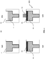
- FIG. 1 shows a method 10 according to a general embodiment of the invention.
- the method 10 is suitable for integrating an MRAM device with a copper-based interconnect structure.
- FIG. 1 shows how an MRAM stack 14 (of the MRAM device) can be integrated with a copper plug 11 (of the copper-based interconnect structure).
- FIG. i(a) shows that, initially, a copper plug 11 is provided.
- the copper plug 11 may include copper one or more plugs, copper vias, copper lines, or other copper elements belonging to the copper-based interconnect structure.
- the copper plug 11 may have a top surface, onto which further processing is performed in the following.
- FIG. i(b) shows a step of forming a recess 12 in the top part (at the top surface) of the copper plug 11.
- the recess 12 may be formed by controlled etching, particularly cyclic etching, more particularly cyclic wet etching, of the copper material at the top surface of the copper plug 11.
- FIG. i(c) shows a step of forming an embedded layer 13 in the recess 12.
- the embedded layer 13 may be deposited into the recess 12, e.g. by atomic layer deposition (ALD), chemical vapour deposition (CVD), physical vapour deposition (PVD), or similar conventional deposition techniques.
- the embedded layer 13 may comprises a titanium layer, a titanium nitride layer, a tantalum layer, a tantalum nitride layer, and/or a tungsten layer.
- FIG. i(d) shows a step of fabricating the MRAM stack 14 on top of the embedded layer 13, in order to proceed towards forming the MRAM device.
- the copper plug 11 thereby functions as the bottom electrode of the MRAM device, and is connected to the MRAM stack 14 from below.
- the MRAM stack 14 may comprises a MTJ stack, which may include two magnetic layers that sandwich a tunnel barrier.
- the embedded layer 13 may be connected, from below, to the lower magnetic layer (e.g. a magnetic free layer).
- the tunnel barrier e.g., comprising MgO
- the upper magnetic layer e.g. a magnetic reference layer
- a top electrode may be formed on the upper magnetic layer (e.g., comprising Co, or CoFeB).
- FIG. i(d) also shows the integrated device 100 that is obtained.
- the integrated device 100 comprises the copper plug 11 of the interconnect structure, and the embedded layer 13, which is formed in the recess 12 in the top part of the copper plug 11. Further, the integrated device 100 comprises the MRAM stack 14 arranged on the embedded layer 13.
- the MRAM device includes the MRAM stack 14 and the copper plug 11, wherein the copper plug 11 forms a bottom electrode of the MRAM device.
- FIGs. 2-7 show the method 10 according to a specific embodiment of the invention, which bases on the general embodiment shown in FIG. 1 .
- the FIGs. 2-7 show, in particular, multiple detailed steps of the method 10 according to this specific embodiment.
- an MRAM device is integrated into a process flow (comprising method 10) of creating two copper-based interconnect structures, which are arranged one above the other, e.g. on different layers of a device or chip.
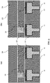
- FIG. 2(a) shows that, initially, two (or more) copper plugs 11 maybe provided (e.g., each copper plug 11 providing a surface with copper trenches or vias).
- the copper plugs 11 may each be surrounded by a barrier 22 (e.g., comprising TaN), and may each be embedded into a dielectric material (e.g., comprising an oxide, like SiOx).
- FIG. 2(b) shows the formation of a recess 12 in the top part of each copper plug 11.
- a controlled copper recess process may be performed.
- the copper recess process may comprise a cyclic controlled oxidation of the copper (surface), e.g. via a wet oxidizer chemistry. This may be followed by a controlled removal of the oxidized copper layer, e.g. via a wet etch chemistry.
- the depth of the copper recess 12, which may be about 20-30 nm, has a good reproducibility, due to the oxidation/etch process, which has a highly controlled sub-nanometer per cycle recess control.
- FIG. 2(c) shows that, after forming the recesses 12, embedded layer material 13a (e.g., comprising TaN) is deposited into each recess 12 and over the entire surface of the intermediate structure obtained after FIG. 2(b) .
- the deposition of the embedded layer material 13a may include a pre-clean process of the recesses 12.
- FIG. 2(d) shows that CMP is the performed on the embedded layer material 13a, in order to form an embedded layer 13 in the recess 12 of each copper plug 11.
- an ultra-smooth surface of each embedded layer 13 may thus be obtained.
- the CMP may stop on the surface of the dielectric material 21.
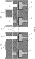
- FIG. 3(a) shows that an MRAM stack layer 14a is then formed on the surface of the embedded layers 13 and on the surface of the dielectric material 21 surrounding the copper plugs 11. Further, a hardmask layer material 31a (e.g., comprising TiN) is formed on the memory stack layer 14a.
- a hardmask layer material 31a e.g., comprising TiN
- FIG. 3(b) shows that the hardmask layer material 31a and the MRAM stack layer 14a are then patterned, in order to obtain an MRAM stack 14 on at least one of the copper plugs 11 (here only the left copper plug 11), in particular on top of the embedded layer 13 of that copper plug 11. Further, a hardmask layer 31 is formed on the MRAM stack 14.
- the hardmask layer e.g., TiN layer
- the hardmask layer may function as top electrode of the MRAM device. That means, the MRAM device may be formed by the copper plug 11/embedded layer 13 (functioning as bottom electrode), the MRAM stack (e.g., comprising a MTJ), and the hardmask layer 31 (functioning as top electrode).
- the pattering may be carried out by using a single lithographic exposure.
- the hardmask layer material 31a and the MRAM stack layer 14a are completely removed, exposing again the surface embedded layer 13.
- the surface of the dielectric material 21 is also exposed.
- FIG. 4(a) shows that the MRAM device is then encapsulated by an encapsulation layer 41 (e.g., comprising SiN), which is formed on the exposed top surfaces of the MRAM device and the intermediate structure obtained in FIG. 3(b) , respectively, and on the side surfaces of the MRAM device.
- an encapsulation layer 41 e.g., comprising SiN
- FIG. 4(b) shows a gap/fill deposition of additional dielectric material 42 (e.g., comprising oxide like SiOx) followed by CMP, so that the entire intermediate structure shown in FIG. 4(b) has a level upper surface. Specifically, a top surface of the additional dielectric material 42 and a top surface of the encapsulated MRAM device are aligned.
- additional dielectric material 42 e.g., comprising oxide like SiOx
- FIG. 5(a) shows that a barrier layer 51 (e.g., comprising SiN) is formed on the top surface of the intermediate structure obtained in FIG. 4(b) , and that further dielectric material 52 (e.g., comprising oxide like SiOx) is deposited onto the barrier layer 51.
- the further dielectric material 52 maybe used for a following dual Damascene process.
- FIG. 5(b) shows that a hardmask 53 (e.g., comprising TiN) is formed on the top surface of the further dielectric material 52.
- a hardmask 53 e.g., comprising TiN
- FIG. 6(a) shows that by performing lithography and etching, for implementing a dual damascene process, a first trench 61 is formed over the copper plug 11 not carrying an MRAM device (here the right copper plug 11).
- the first trench 61 is formed through the further dielectric material 52, the barrier layer 51, and the additional dielectric material 42, and lands on the encapsulation layer 41 provided on the embedded layer 13 of that plug 11.
- FIG. 6(b) shows that a second trench 62 may be formed by lithography and etching, for implementing the dual damascene process.
- the second trench 62 may be formed over the copper plug 11 carrying the MRAM device (here the left copper plug 11).
- the second trench 62 is formed through the further dielectric material 52 and the barrier layer 51, and lands on the hardmask layer 31 functioning as top electrode of the MRAM device.
- FIG. 7 shows that the sider surfaces and bottom surfaces exposed by/inside the first trench 61 and the second trench 62, respectively, are provided with a barrier 72 (e.g., comprising TaN). Then, the first trench 61 and the second trench 62 are filled with copper material (for forming a further copper plug 71, or a copper line, of an upper copper-based interconnect structure), and CMP may be applied to the copper material for the further copper plug 71, or copper line, to finish the dual Damascene process.
- the MRAM device is thus embedded between the lower copper-based interconnect structure including the copper plugs 11 and the upper copper-based interconnect structure including the copper plugs 71, or copper lines.
- the embodiments of the invention provide a new integration scheme for an MRAM device and at least one copper-based interconnect structure.
- the new integrations scheme is less complex (process-wise, i.e. the method 10) and results in a more compact integrate device 100.
Landscapes
- Engineering & Computer Science (AREA)
- Manufacturing & Machinery (AREA)
- Mram Or Spin Memory Techniques (AREA)
- Internal Circuitry In Semiconductor Integrated Circuit Devices (AREA)
Abstract
The present invention relates to Magnetoresistive Random Access Memory (MRAM) devices. The invention provides a method for integrating an MRAM device with a copper-based interconnect structure. Further, the invention provides an integrated device, which comprises an MRAM device integrated with a copper-based interconnect structure. The method comprises forming a recess in a top part of a copper plug of the interconnect structure, forming an embedded layer in the recess, and fabricating an MRAM stack on the embedded layer to form the MRAM device, wherein the copper plug forms a bottom electrode of the MRAM device.
Description
- Generally, the present invention relates to memory devices, in particular to Magnetoresistive Random Access Memory (MRAM) devices. The invention provides a method for integrating an MRAM device with a copper-based interconnect structure. Further, the invention provides an integrated device, which comprises an MRAM device integrated with a copper-based interconnect structure.
- A conventional scheme of integrating an MRAM device with a copper-based interconnect structure, in the back end of line (BEOL), requires a bottom electrode (BE) made of tungsten (W) or another metal, to connect the MRAM device to the interconnect structure, e.g., to standard Cu lines/plugs of the interconnect structure. In particular, in this conventional integration scheme, a smooth surface of the bottom electrode (BE) is created.
-
FIG. 8 illustrates the conventional integration scheme. In particular,FIG. 8 shows a final integrateddevice 80, which comprises acopper plug 81 of the copper-based interconnect structure, and anMRAM stack 84 for an MRAM device. To integrate theMRAM stack 84 with thecopper plug 81, the BE 82 (typically made of W) is provided on top of thecopper plug 81. Further an embedded layer 83 (typically made of TaN) is provided at the top surface of theBE 82. TheBE 82 is, to this end, recessed, subsequently filled with the embedded layer material, and finally chemical mechanical polishing (CMP) is applied to obtain a smooth surface of the embeddedlayer 83. Further, theMRAM stack 84 is then provided on the embeddedlayer 83. - Disadvantageously, this conventional integration scheme requires critical lithography operations (high cost), and at minimum ten extra process operations to create the
BE 82. Further, as it can be derived fromFIG. 8 , theBE 82 adds significantly to the thickness of the MRAM device (it acts as the bottom electrode of the MRAM device connected via the embeddedlayer 83 to the MRAM stack 84). This is highly undesirable, in particular, for advanced technology nodes where ix integration schemes do not have the vertical space for using this kind ofBE 82. - In view of the above-mentioned disadvantages, embodiments of the present invention aim to provide an improved scheme of integrating an MRAM device with a copper-based interconnect structure. An objective is in particular to simplify a method for realizing the integration. Further, a goal is to reduce a thickness of the integrated device, and specifically of the MRAM device. Thus, one desire is to find an alternative to the BE required in the conventional integration scheme. The method should also enable 1x integration schemes implemented with aggressive vertical pitches/dimensions.
- The objective is achieved by the embodiments of the invention provided in the enclosed independent claims. Advantageous implementations of these embodiments are defined in the dependent claims.
- In particular, the embodiments of the invention base on creating a smooth surface directly on a copper (Cu) plug of the copper-based interconnect structure. This means that the MRAM stack can be arranged directly on top of the copper plug.
- A first aspect of the invention provides a method for integrating a MRAM device with a copper-based interconnect structure, the method comprising: forming a recess in a top part of a copper plug of the interconnect structure, forming an embedded layer in the recess, and fabricating an MRAM stack on the embedded layer to form the MRAM device, wherein the contact plug forms a bottom electrode of the MRAM device.
- The "copper plug" may include multiple copper plugs, one or more copper lines, or one or more copper vias, of the copper-based interconnect structure.
- The embedded layer may provide a smooth surface at the top of the copper plug. Thus, the MRAM stack can be provided directly on the copper-based interconnect structure with good contact. Thereby, at least ten processing operations are eliminated, and also one or more additional, cost heavy lithography operations can be eliminated, which would have been needed to create, e.g. the
BE 82. This results in a more industry friendly integration scheme. - Furthermore, the BE provided in the conventional integration scheme between the copper-based interconnect structure and the MRAM stack is eliminated, thus making the integrated device much more compact. In particular, the MRAM device, which comprises the MRAM stack and the copper plug functioning as bottom electrode, can be made much thinner than in the conventional integration scheme.
- In an implementation of the method, the embedded layer comprises a titanium layer, titanium nitride layer, tantalum layer, tantalum nitride layer, and/or tungsten layer.
- These materials allow to create a particular smooth embedded layer surface, and provide a particular good contact between the copper plug and the MRAM stack.
- In an implementation of the method, the MRAM stack comprises a Magnetic Tunnel Junction (MTJ) stack, which includes two magnetic layers that sandwich a tunnel barrier, and the MTJ stack is fabricated directly on the embedded layer.
- In an implementation of the method, fabricating the MRAM stack on the embedded layer is performed in a single mask flow.
- In the conventional integration scheme, fabricating the MRAM stack on the copper-based interconnect structure cannot be done in a single mask flow, since the fabrication of the additional BE requires at least one extra mask and lithography step. Thus, the conventional integration scheme is more complex and costly.
- In an implementation, the method further comprises: pre-cleaning the recess, before depositing the embedded layer into the recess.
- This leads to a significantly better contact/interface between the copper plug and the embedded layer.
- In an implementation of the method, the pre-cleaning and the depositing of the embedded layer are performed in-situ without an air break in between.
- This leads to a higher quality embedded layer, which may, for example, be fabricated by deposition.
- In an implementation of the method, the pre-cleaning comprises argon sputtering of the recess.
- Such a pre-cleaning technique can be easily and efficiently performed in-situ.
- In an implementation of the method, the recess is formed by dry etching or wet etching, in particular by cyclic dry or wet etching.
- This enables a highly controlled recess process of the top part of the copper plug, thus making the formation of the embedded layer directly on copper very feasible.
- In an implementation of the method, the recess has a depth of 20-30 nm into the top part of the copper plug.
- These depths allow to create the embedded layer with a very smooth surface, on the one hand, while on the other hand also guaranteeing a good contact between the copper plug and the MRAM stack.
- In an implementation, the method further comprises: smoothing the surface of the embedded layer, before fabricating the MRAM stack on the embedded layer.
- This allows creating an ultra-smooth embedded layer surface, for an optimum contact to the MRAM stack.
- In an implementation, the method further comprises: smoothing the surface of the copper plug, before forming the recess in the top part of the copper plug.
- This improves the creation of the recess, and thus improves the quality of the embedded layer.
- In an implementation, the method further comprises: fabricating a further copper plug or a copper line on top of the MRAM device.
- In an implementation of the method, the further copper plug or the copper line is fabricated based on a Damascene process, in particular a dual Damascene process.
- The above implementation forms enable to insert the MRAM device in between two copper-based interconnect structures, which are arranged one above the other, for instance, on different layers of a device or chip.
- A second aspect of the invention provides an integrated device fabricated by using the method according to the first aspect or any implementation form thereof.
- The integrated device can be fabricated using a less complex fabrication method, and thus may enjoy higher yield. Further, the integrated device can be designed more compact than with the conventional integration scheme, in particular because the MRAM device is thinner (less high).
- A third aspect of the invention provides an integrated device including a MRAM device integrated with a copper-based interconnect structure, the integrated device comprising: a copper plug of the interconnect structure, an embedded layer formed in a recess in a top part of the copper plug, and an MRAM stack arranged on the embedded layer, wherein the MRAM device is formed by the MRAM stack and the copper plug, the copper plug forming a bottom electrode of the MRAM device.
- The integrated device according to the third aspect may have, in implementation forms of the integrated device, further features that correspond to the features fabricated in the implementation forms of the method of the first aspect.
- The integrated device can be designed more compact than an integrated device resulting from the conventional integration scheme (see e.g.
FIG. 8 ), in particular since the copper plug forms itself the bottom electrode of the MRAM device, and not theBE 82 as in the conventional integration scheme. - The above described aspects and implementations are explained in the following description of embodiments with respect to the enclosed drawings:
- FIG. 1
- shows a method according to a general embodiment of the invention.
- FIG. 2
- shows steps of a method according to a specific embodiment of the invention.
- FIG. 3
- shows further steps of the method according to the specific embodiment of the invention.
- FIG. 4
- shows further steps of the method according to the specific embodiment of the invention.
- FIG. 5
- shows further steps of the method according to the specific embodiment of the invention.
- FIG. 6
- shows further steps of the method according to the specific embodiment of the invention.
- FIG. 7
- shows further steps of the method according to the specific embodiment of the invention.
- FIG. 8
- shows an integrated device according to a conventional integration scheme.
-
FIG. 1 shows amethod 10 according to a general embodiment of the invention. In particular, themethod 10 is suitable for integrating an MRAM device with a copper-based interconnect structure. In particular,FIG. 1 shows how an MRAM stack 14 (of the MRAM device) can be integrated with a copper plug 11 (of the copper-based interconnect structure). - FIG. i(a) shows that, initially, a
copper plug 11 is provided. Thecopper plug 11 may include copper one or more plugs, copper vias, copper lines, or other copper elements belonging to the copper-based interconnect structure. Thecopper plug 11 may have a top surface, onto which further processing is performed in the following. - FIG. i(b) shows a step of forming a
recess 12 in the top part (at the top surface) of thecopper plug 11. Therecess 12 may be formed by controlled etching, particularly cyclic etching, more particularly cyclic wet etching, of the copper material at the top surface of thecopper plug 11. - FIG. i(c) shows a step of forming an embedded
layer 13 in therecess 12. The embeddedlayer 13 may be deposited into therecess 12, e.g. by atomic layer deposition (ALD), chemical vapour deposition (CVD), physical vapour deposition (PVD), or similar conventional deposition techniques. The embeddedlayer 13 may comprises a titanium layer, a titanium nitride layer, a tantalum layer, a tantalum nitride layer, and/or a tungsten layer. - FIG. i(d) shows a step of fabricating the
MRAM stack 14 on top of the embeddedlayer 13, in order to proceed towards forming the MRAM device. Thecopper plug 11 thereby functions as the bottom electrode of the MRAM device, and is connected to theMRAM stack 14 from below. TheMRAM stack 14 may comprises a MTJ stack, which may include two magnetic layers that sandwich a tunnel barrier. The embeddedlayer 13 may be connected, from below, to the lower magnetic layer (e.g. a magnetic free layer). The tunnel barrier (e.g., comprising MgO) may be provided on this lower magnetic layer (e.g., comprising Co or CoFeB), and the upper magnetic layer (e.g. a magnetic reference layer) may be provided on the tunnel barrier, and a top electrode may be formed on the upper magnetic layer (e.g., comprising Co, or CoFeB). - FIG. i(d) also shows the
integrated device 100 that is obtained. Theintegrated device 100 comprises thecopper plug 11 of the interconnect structure, and the embeddedlayer 13, which is formed in therecess 12 in the top part of thecopper plug 11. Further, theintegrated device 100 comprises theMRAM stack 14 arranged on the embeddedlayer 13. The MRAM device includes theMRAM stack 14 and thecopper plug 11, wherein thecopper plug 11 forms a bottom electrode of the MRAM device. -
FIGs. 2-7 show themethod 10 according to a specific embodiment of the invention, which bases on the general embodiment shown inFIG. 1 . TheFIGs. 2-7 show, in particular, multiple detailed steps of themethod 10 according to this specific embodiment. As shown in theFIGs. 2-7 , an MRAM device is integrated into a process flow (comprising method 10) of creating two copper-based interconnect structures, which are arranged one above the other, e.g. on different layers of a device or chip. -
FIG. 2(a) shows that, initially, two (or more) copper plugs 11 maybe provided (e.g., eachcopper plug 11 providing a surface with copper trenches or vias). The copper plugs 11 may each be surrounded by a barrier 22 (e.g., comprising TaN), and may each be embedded into a dielectric material (e.g., comprising an oxide, like SiOx). -
FIG. 2(b) shows the formation of arecess 12 in the top part of eachcopper plug 11. In particular, a controlled copper recess process may be performed. The copper recess process may comprise a cyclic controlled oxidation of the copper (surface), e.g. via a wet oxidizer chemistry. This may be followed by a controlled removal of the oxidized copper layer, e.g. via a wet etch chemistry. The depth of thecopper recess 12, which may be about 20-30 nm, has a good reproducibility, due to the oxidation/etch process, which has a highly controlled sub-nanometer per cycle recess control. -
FIG. 2(c) shows that, after forming therecesses 12, embeddedlayer material 13a (e.g., comprising TaN) is deposited into eachrecess 12 and over the entire surface of the intermediate structure obtained afterFIG. 2(b) . In particular, the deposition of the embeddedlayer material 13a may include a pre-clean process of therecesses 12. -
FIG. 2(d) shows that CMP is the performed on the embeddedlayer material 13a, in order to form an embeddedlayer 13 in therecess 12 of eachcopper plug 11. In particular, an ultra-smooth surface of each embeddedlayer 13 may thus be obtained. The CMP may stop on the surface of thedielectric material 21. -
FIG. 3(a) shows that anMRAM stack layer 14a is then formed on the surface of the embeddedlayers 13 and on the surface of thedielectric material 21 surrounding the copper plugs 11. Further, ahardmask layer material 31a (e.g., comprising TiN) is formed on thememory stack layer 14a. -
FIG. 3(b) shows that thehardmask layer material 31a and theMRAM stack layer 14a are then patterned, in order to obtain anMRAM stack 14 on at least one of the copper plugs 11 (here only the left copper plug 11), in particular on top of the embeddedlayer 13 of thatcopper plug 11. Further, ahardmask layer 31 is formed on theMRAM stack 14. The hardmask layer (e.g., TiN layer) may function as top electrode of the MRAM device. That means, the MRAM device may be formed by thecopper plug 11/embedded layer 13 (functioning as bottom electrode), the MRAM stack (e.g., comprising a MTJ), and the hardmask layer 31 (functioning as top electrode). The pattering may be carried out by using a single lithographic exposure. On the at least onecopper plug 11 on which noMRAM stack 14 is formed (here the right copper plug 11) thehardmask layer material 31a and theMRAM stack layer 14a are completely removed, exposing again the surface embeddedlayer 13. The surface of thedielectric material 21 is also exposed. -
FIG. 4(a) shows that the MRAM device is then encapsulated by an encapsulation layer 41 (e.g., comprising SiN), which is formed on the exposed top surfaces of the MRAM device and the intermediate structure obtained inFIG. 3(b) , respectively, and on the side surfaces of the MRAM device. -
FIG. 4(b) shows a gap/fill deposition of additional dielectric material 42 (e.g., comprising oxide like SiOx) followed by CMP, so that the entire intermediate structure shown inFIG. 4(b) has a level upper surface. Specifically, a top surface of the additionaldielectric material 42 and a top surface of the encapsulated MRAM device are aligned. -
FIG. 5(a) shows that a barrier layer 51 (e.g., comprising SiN) is formed on the top surface of the intermediate structure obtained inFIG. 4(b) , and that further dielectric material 52 (e.g., comprising oxide like SiOx) is deposited onto thebarrier layer 51. The furtherdielectric material 52 maybe used for a following dual Damascene process. -
FIG. 5(b) shows that a hardmask 53 (e.g., comprising TiN) is formed on the top surface of the furtherdielectric material 52. -
FIG. 6(a) shows that by performing lithography and etching, for implementing a dual damascene process, afirst trench 61 is formed over thecopper plug 11 not carrying an MRAM device (here the right copper plug 11). Thefirst trench 61 is formed through the furtherdielectric material 52, thebarrier layer 51, and the additionaldielectric material 42, and lands on theencapsulation layer 41 provided on the embeddedlayer 13 of thatplug 11. -
FIG. 6(b) shows that asecond trench 62 may be formed by lithography and etching, for implementing the dual damascene process. Thesecond trench 62 may be formed over thecopper plug 11 carrying the MRAM device (here the left copper plug 11). Thesecond trench 62 is formed through the furtherdielectric material 52 and thebarrier layer 51, and lands on thehardmask layer 31 functioning as top electrode of the MRAM device. -
FIG. 7 shows that the sider surfaces and bottom surfaces exposed by/inside thefirst trench 61 and thesecond trench 62, respectively, are provided with a barrier 72 (e.g., comprising TaN). Then, thefirst trench 61 and thesecond trench 62 are filled with copper material (for forming afurther copper plug 71, or a copper line, of an upper copper-based interconnect structure), and CMP may be applied to the copper material for thefurther copper plug 71, or copper line, to finish the dual Damascene process. The MRAM device is thus embedded between the lower copper-based interconnect structure including the copper plugs 11 and the upper copper-based interconnect structure including the copper plugs 71, or copper lines. - In summary, the embodiments of the invention provide a new integration scheme for an MRAM device and at least one copper-based interconnect structure. The new integrations scheme is less complex (process-wise, i.e. the method 10) and results in a more compact integrate
device 100.
Claims (15)
- Method (10) for integrating a Magnetoresistive Random Access Memory, MRAM, device with a copper-based interconnect structure, the method (10) comprising:forming a recess (12) in a top part of a copper plug (11) of the interconnect structure,forming an embedded layer (13) in the recess (12), andfabricating an MRAM stack (14) on the embedded layer (13) to form the MRAM device, wherein the copper plug (11) forms a bottom electrode of the MRAM device.
- The method (10) according to claim 1, wherein:
the embedded layer (13) comprises a titanium layer, titanium nitride layer, tantalum layer, tantalum nitride layer, and/or tungsten layer. - The method (10) according to claim 1 or 2, wherein:the MRAM stack (14) comprises a Magnetic Tunnel Junction, MTJ, stack, which includes two magnetic layers that sandwich a tunnel barrier, andthe MTJ stack (14) is fabricated directly on the embedded layer (13).
- Method (10) according to one of the claims 1 to 3, wherein:
fabricating the MRAM stack (14) on the embedded layer (13) is performed in a single mask flow. - Method (10) according to one of the claims 1 to 4, further comprising:
pre-cleaning the recess (12), before depositing the embedded layer (13) into the recess. - Method (10) according to claim 5, wherein:
the pre-cleaning and the depositing of the embedded layer (13) are performed in-situ without an air break in between. - Method (10) according to claim 5 or 6, wherein:
the pre-cleaning comprises argon sputtering of the recess (12). - Method (10) according to one of the claims 1 to 7, wherein:
the recess (12) is formed by dry etching or wet etching, in particular by cyclic dry or wet etching. - Method (10) according to one of the claims 1 to 8, wherein:
the recess (12) has a depth of 20-30 nm into the top part of the copper plug. - Method (10) according to one of the claims 1 to 9, further comprising:
smoothing the surface of the embedded layer (13), before fabricating the MRAM stack (14) on the embedded layer (13). - Method (10) according to one of the claims 1 to 10, further comprising:
smoothing the surface of the copper plug (11), before forming the recess (12) in the top part of the copper plug (11). - Method according to one of the claims 1 to 11, further comprising:
fabricating a further copper plug (71) or a copper line on top of the MRAM device. - Method (10) according to claim 12, wherein:
the further copper plug (71) or the copper line is fabricated based on a Damascene process. - Integrated device (100) fabricated by using the method (10) according to any one of the claims 1 to 13.
- Integrated device (100) including a Magnetoresistive Random Access Memory, MRAM, device integrated with a copper-based interconnect structure, the integrated device (100) comprising:a copper plug (11) of the interconnect structure,an embedded layer (13) formed in a recess (12) in a top part of the copper plug (11), andan MRAM stack (14) arranged on the embedded layer (13),wherein the MRAM device is formed by the MRAM stack (14) and the copper plug (11), the copper plug (11) forming a bottom electrode of the MRAM device.
Priority Applications (1)
| Application Number | Priority Date | Filing Date | Title |
|---|---|---|---|
| EP19214053.1A EP3832743A1 (en) | 2019-12-06 | 2019-12-06 | Integrating an mram device with a copper-based interconnect structure |
Applications Claiming Priority (1)
| Application Number | Priority Date | Filing Date | Title |
|---|---|---|---|
| EP19214053.1A EP3832743A1 (en) | 2019-12-06 | 2019-12-06 | Integrating an mram device with a copper-based interconnect structure |
Publications (1)
| Publication Number | Publication Date |
|---|---|
| EP3832743A1 true EP3832743A1 (en) | 2021-06-09 |
Family
ID=68808127
Family Applications (1)
| Application Number | Title | Priority Date | Filing Date |
|---|---|---|---|
| EP19214053.1A Withdrawn EP3832743A1 (en) | 2019-12-06 | 2019-12-06 | Integrating an mram device with a copper-based interconnect structure |
Country Status (1)
| Country | Link |
|---|---|
| EP (1) | EP3832743A1 (en) |
Cited By (1)
| Publication number | Priority date | Publication date | Assignee | Title |
|---|---|---|---|---|
| CN116018049A (en) * | 2021-10-20 | 2023-04-25 | 浙江驰拓科技有限公司 | A spin-orbit torque magnetoresistive random access memory and its manufacturing method |
Citations (4)
| Publication number | Priority date | Publication date | Assignee | Title |
|---|---|---|---|---|
| US20150357559A1 (en) * | 2014-06-05 | 2015-12-10 | Everspin Technologies, Inc. | Top electrode coupling in a magnetoresistive device using an etch stop layer |
| US20170062521A1 (en) * | 2015-09-01 | 2017-03-02 | Kabushiki Kaisha Toshiba | Magnetic memory device and method of manufacturing the same |
| CN109994602A (en) * | 2018-01-03 | 2019-07-09 | 上海磁宇信息科技有限公司 | A method of preparing magnetic RAM memory unit and logic unit |
| CN109994601A (en) * | 2018-01-03 | 2019-07-09 | 上海磁宇信息科技有限公司 | A method of making magnetic RAM circuit connection |
-
2019
- 2019-12-06 EP EP19214053.1A patent/EP3832743A1/en not_active Withdrawn
Patent Citations (4)
| Publication number | Priority date | Publication date | Assignee | Title |
|---|---|---|---|---|
| US20150357559A1 (en) * | 2014-06-05 | 2015-12-10 | Everspin Technologies, Inc. | Top electrode coupling in a magnetoresistive device using an etch stop layer |
| US20170062521A1 (en) * | 2015-09-01 | 2017-03-02 | Kabushiki Kaisha Toshiba | Magnetic memory device and method of manufacturing the same |
| CN109994602A (en) * | 2018-01-03 | 2019-07-09 | 上海磁宇信息科技有限公司 | A method of preparing magnetic RAM memory unit and logic unit |
| CN109994601A (en) * | 2018-01-03 | 2019-07-09 | 上海磁宇信息科技有限公司 | A method of making magnetic RAM circuit connection |
Cited By (1)
| Publication number | Priority date | Publication date | Assignee | Title |
|---|---|---|---|---|
| CN116018049A (en) * | 2021-10-20 | 2023-04-25 | 浙江驰拓科技有限公司 | A spin-orbit torque magnetoresistive random access memory and its manufacturing method |
Similar Documents
| Publication | Publication Date | Title |
|---|---|---|
| TWI683419B (en) | Integrated circuit and method for forming the same | |
| JP5089575B2 (en) | Interconnect structure and method of manufacturing the same | |
| TWI610343B (en) | Semiconductor structure with wedge-shaped mosaic holes and manufacturing method thereof | |
| US7193327B2 (en) | Barrier structure for semiconductor devices | |
| KR101130557B1 (en) | Interconnect structure and process of making the same | |
| TW200415747A (en) | Air gap dual damascene process and structure | |
| TW201532247A (en) | A cost-effective method of forming embedded dynamic random access memory capacitors | |
| TW201717278A (en) | Self-aligned gate contact with selective etch stop pad | |
| US8492269B2 (en) | Hybrid contact structure with low aspect ratio contacts in a semiconductor device | |
| US9570397B1 (en) | Local interconnect structure including non-eroded contact via trenches | |
| JP7588638B2 (en) | Encapsulated topography-assisted self-aligned MRAM top contact | |
| US20150311113A1 (en) | Trench structure for high performance interconnection lines of different resistivity and method of making same | |
| CN109524348B (en) | Perfectly aligned vias in ground rule areas | |
| CN101471285B (en) | Semiconductor device and method for manufacturing the device | |
| CN203659847U (en) | Integrated circuit device | |
| US7544609B2 (en) | Method for integrating liner formation in back end of line processing | |
| US20050266679A1 (en) | Barrier structure for semiconductor devices | |
| JP4231055B2 (en) | Semiconductor device and manufacturing method thereof | |
| KR100720515B1 (en) | Method of forming copper metal wiring with local barrier metal layer | |
| TW202245193A (en) | Semiconductor structure and method for manufacturing the same | |
| TW201528428A (en) | Semiconductor structure and method of manufacturing same | |
| US10825720B2 (en) | Single trench damascene interconnect using TiN HMO | |
| TWI838721B (en) | Subtractive metal etch with improved isolation for beol interconnect and cross point | |
| US20240188448A1 (en) | Multiple layers of void-free interlayer dielectric between adjacent magnetoresistive random-access memory devices | |
| JP2000232106A (en) | Semiconductor device and method of manufacturing semiconductor device |
Legal Events
| Date | Code | Title | Description |
|---|---|---|---|
| PUAI | Public reference made under article 153(3) epc to a published international application that has entered the european phase |
Free format text: ORIGINAL CODE: 0009012 |
|
| STAA | Information on the status of an ep patent application or granted ep patent |
Free format text: STATUS: THE APPLICATION HAS BEEN PUBLISHED |
|
| AK | Designated contracting states |
Kind code of ref document: A1 Designated state(s): AL AT BE BG CH CY CZ DE DK EE ES FI FR GB GR HR HU IE IS IT LI LT LU LV MC MK MT NL NO PL PT RO RS SE SI SK SM TR |
|
| STAA | Information on the status of an ep patent application or granted ep patent |
Free format text: STATUS: THE APPLICATION IS DEEMED TO BE WITHDRAWN |
|
| 18D | Application deemed to be withdrawn |
Effective date: 20211210 |