EP3832735A2 - Multilayer high-k gate dielectric for a high performance logic transistor - Google Patents
Multilayer high-k gate dielectric for a high performance logic transistor Download PDFInfo
- Publication number
- EP3832735A2 EP3832735A2 EP20198182.6A EP20198182A EP3832735A2 EP 3832735 A2 EP3832735 A2 EP 3832735A2 EP 20198182 A EP20198182 A EP 20198182A EP 3832735 A2 EP3832735 A2 EP 3832735A2
- Authority
- EP
- European Patent Office
- Prior art keywords
- gate dielectric
- fin
- multilayer
- gate
- dielectric stack
- Prior art date
- Legal status (The legal status is an assumption and is not a legal conclusion. Google has not performed a legal analysis and makes no representation as to the accuracy of the status listed.)
- Pending
Links
Images







Classifications
-
- H—ELECTRICITY
- H10—SEMICONDUCTOR DEVICES; ELECTRIC SOLID-STATE DEVICES NOT OTHERWISE PROVIDED FOR
- H10D—INORGANIC ELECTRIC SEMICONDUCTOR DEVICES
- H10D30/00—Field-effect transistors [FET]
- H10D30/60—Insulated-gate field-effect transistors [IGFET]
- H10D30/62—Fin field-effect transistors [FinFET]
-
- H—ELECTRICITY
- H10—SEMICONDUCTOR DEVICES; ELECTRIC SOLID-STATE DEVICES NOT OTHERWISE PROVIDED FOR
- H10D—INORGANIC ELECTRIC SEMICONDUCTOR DEVICES
- H10D64/00—Electrodes of devices having potential barriers
- H10D64/60—Electrodes characterised by their materials
- H10D64/66—Electrodes having a conductor capacitively coupled to a semiconductor by an insulator, e.g. MIS electrodes
- H10D64/68—Electrodes having a conductor capacitively coupled to a semiconductor by an insulator, e.g. MIS electrodes characterised by the insulator, e.g. by the gate insulator
- H10D64/681—Electrodes having a conductor capacitively coupled to a semiconductor by an insulator, e.g. MIS electrodes characterised by the insulator, e.g. by the gate insulator having a compositional variation, e.g. multilayered
- H10D64/683—Electrodes having a conductor capacitively coupled to a semiconductor by an insulator, e.g. MIS electrodes characterised by the insulator, e.g. by the gate insulator having a compositional variation, e.g. multilayered being parallel to the channel plane
-
- H—ELECTRICITY
- H10—SEMICONDUCTOR DEVICES; ELECTRIC SOLID-STATE DEVICES NOT OTHERWISE PROVIDED FOR
- H10D—INORGANIC ELECTRIC SEMICONDUCTOR DEVICES
- H10D30/00—Field-effect transistors [FET]
- H10D30/01—Manufacture or treatment
- H10D30/021—Manufacture or treatment of FETs having insulated gates [IGFET]
- H10D30/024—Manufacture or treatment of FETs having insulated gates [IGFET] of fin field-effect transistors [FinFET]
-
- H—ELECTRICITY
- H10—SEMICONDUCTOR DEVICES; ELECTRIC SOLID-STATE DEVICES NOT OTHERWISE PROVIDED FOR
- H10D—INORGANIC ELECTRIC SEMICONDUCTOR DEVICES
- H10D30/00—Field-effect transistors [FET]
- H10D30/60—Insulated-gate field-effect transistors [IGFET]
- H10D30/62—Fin field-effect transistors [FinFET]
- H10D30/6211—Fin field-effect transistors [FinFET] having fin-shaped semiconductor bodies integral with the bulk semiconductor substrates
-
- H—ELECTRICITY
- H10—SEMICONDUCTOR DEVICES; ELECTRIC SOLID-STATE DEVICES NOT OTHERWISE PROVIDED FOR
- H10D—INORGANIC ELECTRIC SEMICONDUCTOR DEVICES
- H10D30/00—Field-effect transistors [FET]
- H10D30/60—Insulated-gate field-effect transistors [IGFET]
- H10D30/67—Thin-film transistors [TFT]
- H10D30/6729—Thin-film transistors [TFT] characterised by the electrodes
- H10D30/673—Thin-film transistors [TFT] characterised by the electrodes characterised by the shapes, relative sizes or dispositions of the gate electrodes
- H10D30/6735—Thin-film transistors [TFT] characterised by the electrodes characterised by the shapes, relative sizes or dispositions of the gate electrodes having gates fully surrounding the channels, e.g. gate-all-around
-
- H—ELECTRICITY
- H10—SEMICONDUCTOR DEVICES; ELECTRIC SOLID-STATE DEVICES NOT OTHERWISE PROVIDED FOR
- H10D—INORGANIC ELECTRIC SEMICONDUCTOR DEVICES
- H10D64/00—Electrodes of devices having potential barriers
- H10D64/60—Electrodes characterised by their materials
- H10D64/66—Electrodes having a conductor capacitively coupled to a semiconductor by an insulator, e.g. MIS electrodes
- H10D64/68—Electrodes having a conductor capacitively coupled to a semiconductor by an insulator, e.g. MIS electrodes characterised by the insulator, e.g. by the gate insulator
- H10D64/681—Electrodes having a conductor capacitively coupled to a semiconductor by an insulator, e.g. MIS electrodes characterised by the insulator, e.g. by the gate insulator having a compositional variation, e.g. multilayered
- H10D64/685—Electrodes having a conductor capacitively coupled to a semiconductor by an insulator, e.g. MIS electrodes characterised by the insulator, e.g. by the gate insulator having a compositional variation, e.g. multilayered being perpendicular to the channel plane
-
- H—ELECTRICITY
- H10—SEMICONDUCTOR DEVICES; ELECTRIC SOLID-STATE DEVICES NOT OTHERWISE PROVIDED FOR
- H10D—INORGANIC ELECTRIC SEMICONDUCTOR DEVICES
- H10D64/00—Electrodes of devices having potential barriers
- H10D64/60—Electrodes characterised by their materials
- H10D64/66—Electrodes having a conductor capacitively coupled to a semiconductor by an insulator, e.g. MIS electrodes
- H10D64/68—Electrodes having a conductor capacitively coupled to a semiconductor by an insulator, e.g. MIS electrodes characterised by the insulator, e.g. by the gate insulator
- H10D64/691—Electrodes having a conductor capacitively coupled to a semiconductor by an insulator, e.g. MIS electrodes characterised by the insulator, e.g. by the gate insulator comprising metallic compounds, e.g. metal oxides or metal silicates
-
- H—ELECTRICITY
- H10—SEMICONDUCTOR DEVICES; ELECTRIC SOLID-STATE DEVICES NOT OTHERWISE PROVIDED FOR
- H10D—INORGANIC ELECTRIC SEMICONDUCTOR DEVICES
- H10D84/00—Integrated devices formed in or on semiconductor substrates that comprise only semiconducting layers, e.g. on Si wafers or on GaAs-on-Si wafers
- H10D84/01—Manufacture or treatment
- H10D84/0123—Integrating together multiple components covered by H10D12/00 or H10D30/00, e.g. integrating multiple IGBTs
- H10D84/0126—Integrating together multiple components covered by H10D12/00 or H10D30/00, e.g. integrating multiple IGBTs the components including insulated gates, e.g. IGFETs
- H10D84/0158—Integrating together multiple components covered by H10D12/00 or H10D30/00, e.g. integrating multiple IGBTs the components including insulated gates, e.g. IGFETs the components including FinFETs
-
- H—ELECTRICITY
- H10—SEMICONDUCTOR DEVICES; ELECTRIC SOLID-STATE DEVICES NOT OTHERWISE PROVIDED FOR
- H10D—INORGANIC ELECTRIC SEMICONDUCTOR DEVICES
- H10D84/00—Integrated devices formed in or on semiconductor substrates that comprise only semiconducting layers, e.g. on Si wafers or on GaAs-on-Si wafers
- H10D84/01—Manufacture or treatment
- H10D84/02—Manufacture or treatment characterised by using material-based technologies
- H10D84/03—Manufacture or treatment characterised by using material-based technologies using Group IV technology, e.g. silicon technology or silicon-carbide [SiC] technology
- H10D84/038—Manufacture or treatment characterised by using material-based technologies using Group IV technology, e.g. silicon technology or silicon-carbide [SiC] technology using silicon technology, e.g. SiGe
-
- H—ELECTRICITY
- H10—SEMICONDUCTOR DEVICES; ELECTRIC SOLID-STATE DEVICES NOT OTHERWISE PROVIDED FOR
- H10D—INORGANIC ELECTRIC SEMICONDUCTOR DEVICES
- H10D84/00—Integrated devices formed in or on semiconductor substrates that comprise only semiconducting layers, e.g. on Si wafers or on GaAs-on-Si wafers
- H10D84/80—Integrated devices formed in or on semiconductor substrates that comprise only semiconducting layers, e.g. on Si wafers or on GaAs-on-Si wafers characterised by the integration of at least one component covered by groups H10D12/00 or H10D30/00, e.g. integration of IGFETs
- H10D84/82—Integrated devices formed in or on semiconductor substrates that comprise only semiconducting layers, e.g. on Si wafers or on GaAs-on-Si wafers characterised by the integration of at least one component covered by groups H10D12/00 or H10D30/00, e.g. integration of IGFETs of only field-effect components
- H10D84/83—Integrated devices formed in or on semiconductor substrates that comprise only semiconducting layers, e.g. on Si wafers or on GaAs-on-Si wafers characterised by the integration of at least one component covered by groups H10D12/00 or H10D30/00, e.g. integration of IGFETs of only field-effect components of only insulated-gate FETs [IGFET]
- H10D84/834—Integrated devices formed in or on semiconductor substrates that comprise only semiconducting layers, e.g. on Si wafers or on GaAs-on-Si wafers characterised by the integration of at least one component covered by groups H10D12/00 or H10D30/00, e.g. integration of IGFETs of only field-effect components of only insulated-gate FETs [IGFET] comprising FinFETs
-
- H—ELECTRICITY
- H10—SEMICONDUCTOR DEVICES; ELECTRIC SOLID-STATE DEVICES NOT OTHERWISE PROVIDED FOR
- H10D—INORGANIC ELECTRIC SEMICONDUCTOR DEVICES
- H10D64/00—Electrodes of devices having potential barriers
- H10D64/60—Electrodes characterised by their materials
- H10D64/66—Electrodes having a conductor capacitively coupled to a semiconductor by an insulator, e.g. MIS electrodes
- H10D64/68—Electrodes having a conductor capacitively coupled to a semiconductor by an insulator, e.g. MIS electrodes characterised by the insulator, e.g. by the gate insulator
- H10D64/689—Electrodes having a conductor capacitively coupled to a semiconductor by an insulator, e.g. MIS electrodes characterised by the insulator, e.g. by the gate insulator having ferroelectric layers
Definitions
- Embodiments of the disclosure are in the field of integrated circuit structures and, in particular, a multilayer high-k gate dielectric for a high performance logic transistor.
- a gate oxide is a dielectric/insulating layer that separates the gate terminal of the transistor from the underlying source and drain terminals.
- An inversion layer is formed in the semiconductor substrate via capacitive coupling when a gate bias is applied. The inversion layer provides a channel through which current can pass between source and drain terminals.
- Conventional gate oxide scaling has limits that may also limit the inversion charge while meeting all the requirement in the reliability.
- a multilayer high-k gate dielectric for a high performance logic transistor are described.
- numerous specific details are set forth, such as specific material and tooling regimes, in order to provide a thorough understanding of embodiments of the present disclosure. It will be apparent to one skilled in the art that embodiments of the present disclosure may be practiced without these specific details. In other instances, well-known features, such as single or dual damascene processing, are not described in detail in order to not unnecessarily obscure embodiments of the present disclosure. Furthermore, it is to be understood that the various embodiments shown in the Figures are illustrative representations and are not necessarily drawn to scale.
- One or more embodiments described herein are directed to structures and architectures for fabricating a multilayer high-k gate dielectric for a high performance logic transistor, such as a FinFET or gate-all-around FET.
- One or more embodiments described herein are further directed to structures and architectures for fabricating an integrated circuit that utilizes SOI template formation while maintaining the capability of multi-layer high k, enabling high performing & low-leakage transistors.
- Embodiments may include or pertain to one or more of transistors, semiconducting oxide materials, and system-on-chip (SoC) technologies of future technology nodes.
- SoC system-on-chip
- a FinFET is one type of non-planar transistor which is built around a thin strip of semiconductor material (referred to as the "fin").
- the transistor includes the standard field effect transistor (FET) nodes/components: a gate, a gate dielectric, a source region, and a drain region.
- FET field effect transistor
- a conductive channel of the device resides on the outer sides of the fin beneath the gate dielectric. Specifically, current runs along "sidewalls" of the fin as well as along the top side of the fin. Because the conductive channel essentially resides along the three different outer, planar regions of the fin, such a FinFET is typically referred to as a "tri-gate" FinFET.
- Other types of FinFETs exist (such as “double-gate” FinFETs in which the conductive channel principally resides only along both sidewalls of the fin and not along the top side of the fin).
- fabricating a non-planar transistor includes depositing a dielectric material into a given space to form a gate dielectric or oxide to provide at least some electrical insulation between two adjoining structures, e.g., a fin and a gate.
- a common material for a gate dielectric is silicon dioxide, which has a dielectric constant around 3.8.
- a non-planar transistor is fabricated with a multilayer oxide using high-k gate materials and an amorphous layer and/or a crystalline layer, thus enabling a higher inversion charge.
- a non-planar transistor is fabricated with a buried high-k material combined with a pseudo-SOI template.
- Non-planar transistors fabricated using such architectures may exhibit an increase in gate control, stability, and performance of thin film transistors. Applications of such systems may include, but are not limited to, back end (BEOL) logic, memory, or analog applications.
- Embodiments described herein may include non-planar structures that effectively increase gate oxide thickness scaling and inversion charge by integrating a multilayer gate dielectric in unique architectures.
- high-k materials are used for the gate dielectric, where the high-k materials have a dielectric constant k greater than 7.
- the non-planar transistor may comprise any type of multi-gate, nanowire, or nanoribbon device.
- an integrated circuit structure provides a multilayer high-k gate dielectric stack comprising at least a first high-k material and a second high-k material.
- the first high-k material extends conformally over a fin over a channel region, while the second high-k material is conformal to the first high-k material, wherein either the first high-k material or the second high-k material has a modified material property different from the other high-k material, where the modified material property comprises at least one of ferroelectricity, crystalline phase, texturing, ordering orientation of the crystalline phase or texturing to a specific crystalline direction or plane, strain, surface roughness, and lattice constant and combinations thereof.
- a metal gate material is over and on a top most high-k material of the multilayer high-k gate dielectric stack.
- the modified material property may include different crystalline phases, including crystalline, poly crystalline, nanocrystalline, and amorphous.
- the modified strained property may originate from an annealing process or other heat treatment, and extra sequences of sacrificial material deposition and etching, which alters the physical and sometimes chemical properties of a material.
- FIG. 1 shows one example of a portion of an IC device 100 consistent with the present disclosure, in this case a portion of a FinFET.
- IC device 100 includes a substrate 101, a trench dielectric 102 on substrate 101, and a fin structure 110 disposed in a trench which is formed by trench dielectric 102.
- Fin structure 110 comprises, for example, a top surface 114 and a pair of laterally opposite sidewalls (sidewall 111 and opposing sidewall 112, respectively).
- portions of fin structure 110 which are vertically offset from one another comprise different respective group III-V (and/or other) semiconductor materials.
- Substrate 101 is formed of any of a variety of materials that are suitable for use as a substrate of a semiconductor device, and in particular as a substrate for non-planar transistors such as FinFETS and multi-gate transistors.
- suitable materials include silicon (Si), germanium (Ge), silicon-germanium (SiGe), silicon-carbide (SiC), sapphire, a group III-V semiconductor, a silicon on insulate (SOI) substrate, combinations thereof, and the like.
- substrate 101 is formed from or includes single crystal silicon.
- the non-planar semiconductor device includes at least one trench that is formed on or within the substrate.
- a trench (not separately labeled) is defined by the sidewalls of trench dielectric 102 (hereinafter, trench sidewalls) and an upper portion of substrate 101.
- the trench thus includes at least two opposing sides (trench sidewalls) and a bottom.
- a bottom of the trench is formed at least in part by an upper surface of the substrate, and/or one or more buffer and/or transition layers deposited on the substrate.
- a trench of any of a variety of suitable dimensions may be used, in different embodiments, according to implementation-specific details.
- the height (z-axis dimension) and width (y-axis dimension) of the trench enables the deposition of the materials used to form fin structure 110 - e.g., via an aspect ratio trapping (ART) process.
- the width of the trench is in a range of 1 nanometers (nm) to 500 nanometers (nm), such as in a range of 1 nm to 300 nm, in a range of 1 nm to 100 nm, in a range of 5 nm to 100 nm, or even in a range of 5 nm to 30 nm.
- the height of such a trench is range, for example, in a range of 1 nm to 500 nm, such as a range of 100 nm to 300 nm.
- Trench dielectric 102 which may also comprise multiple layers, is formed from any of a variety of materials that are suitable for use as a trench dielectric material of a non-planar semiconductor device.
- Non-limiting examples of such materials include oxides, nitrides and alloys, such as but not limited to silicon oxide (SiO 2 ), silicon nitride (SiN), silicon oxycarbide (SiCO), silicon carbon oxynitride (SiCON), silicon carbonitride (SiCN), combinations thereof, and the like.
- FIG. 2 shows a view of a cross-section X-X' of IC device 100.
- a non-planar transistor of IC device 100 comprises structures which are variously disposed in or on fin structure 110.
- such a non-planar transistor may include a channel structure 113, two doped source or drain (“SD") structures 116, 118 at opposite ends of the channel structure 113, and raised epitaxial (epi) source or drain regions 117, 119.
- SD doped source or drain
- epi epitaxial
- a gate structure of the non-planar transistor comprises gate electrode 162 and a multilayer high-k gate dielectric stack 140 comprising at least a first high-k material 140A and a second high-k material 140B up to an n th high-k material 140N.
- a gate electrode162 is over and on a topmost high-k material in the multilayer high-k gate dielectric stack 140. More particularly, gate electrode 162 extends over and across a portion of fin 110 in a region between insulation spacers 150, 151, which are shown as transparent to further show features of IC device 100.
- either the first high-k material 140A or the second high-k material 140B has a modified material property different from the other high-k material, wherein the modified property comprises at least one of ferroelectricity, crystalline phase, texturing, ordering orientation of the crystalline phase or texturing to a specific crystalline direction or plane, strain, surface roughness, and lattice constant and combinations thereof.
- the crystalline phases include crystalline, polycrystalline, nanocrystalline, and amorphous.
- the second high-k material 140B comprises the same or different material as the first high-k material 140A, but the second high-k material 140B may have a different crystalline phase, strain, surface roughness, and/or lattice constant than the first high-k material 140A.
- a channel treatment may be employed to modify one or more properties of one or more of the high-k materials 140A to 140N.
- annealing or surface texturing or an extra sequence of sacrificial material deposition and etching may be used to modify the strain of one or more of the high-k materials 140A to 140N.
- operation of IC device 100 includes selectively controlling a current between source or drain regions 116, 118 via channel region 113, by applying a voltage to gate electrode 162.
- This functionality is enabled in part by dielectric structures which provide electrical insulation between gate electrode 162 and channel region 113.
- the transistor Due to the interaction between the high-k materials 140A to 140N having different modified properties, the transistor provides a higher current. For example, different materials and dopants, or doping profile, material profile, strain and templating of each layer provides different growth characteristics in each distinct layer and in the whole stack, enabling higher inversion charge through the whole multilayer high-k gate dielectric stack 140. The result is a higher charge may be introduced into the channel 113 and higher current may be achieved for the transistor for higher performance.
- gate electrode 162 includes a metal with a work function below 5 eV.
- the metal gate electrode 162 includes, for example, an elemental metal layer, a metal alloy layer, or laminate structure of either or both.
- the gate electrode 162 may comprise a metal nitride, such as TiN (e.g., 4.0-4.7 eV).
- the gate electrode 162 may also comprise Al (e.g., TiAIN).
- Other alloy constituents may also be employed, such as, but not limited to C, Ta, W, Pt, and Zn.
- the multilayer high-k gate dielectric stack 140 may optionally include an optional underlayer gate dielectric 120 that extends conformally over the fin over the channel region under the multilayer high-k gate dielectric stack.
- the underlayer gate dielectric 120 has a dielectric constant less than the dielectric constant of the materials comprising the multilayer high-k gate dielectric stack 140.
- the underlayer gate dielectric 120 and the multilayer high-k gate dielectric stack 140 provide electrical insulation between gate electrode 162 and each of a top of the channel structure and opposite vertical sidewalls of the channel structure. The presence of underlayer gate dielectric 120, however, may preserve channel mobility by mitigating scattering from higher k material resulting from the use of higher-k materials as gate dielectrics.
- the underlayer dielectric 120 adjoins, and is conformal to, respective portions of the fin 110 sidewalls 111, 112 and top surface 114. In one embodiment, the underlayer dielectric 120 extends past the boundaries of the spacers 150 and 151. However, in the embodiment shown, the underlayer dielectric 120 is present on the fin 110 only within the boundaries of the spacers 150 and 151.
- the multilayer high-k gate dielectric stack 140 comprises at least two high-k material layers.
- the first high-k material 140A extends conformally over the fin over the channel region (and over the underlayer gate dielectric 120 if present), the second high-k material 140B is conformal to the first high-k material 140A, the next high-k material is conformal to the second high-k material 140B, and so on.
- the multilayer high-k gate dielectric stack 140 includes portions that variously extend each between gate electrode 162, a top of underlayer dielectric 120, and respective inner sidewalls of insulation spacers 150 and 151. It is noted that underlayer dielectric 120 is not conformal to the sides of insulation spacer 150, 151.
- a method for fabricating an IC device configured with transistor functionality may include forming a fin that extends up from a substrate, the fin comprising source and drain regions, and a channel region between the source and drain regions.
- a multilayer high-k gate dielectric stack is formed comprising at least a first high-k material and a second high-k material, the first high-k material extending conformally over the fin over the channel region, and the second high-k material conformal to the first high-k material, wherein either the first high-k material or the second high-k material has a modified property different from the other high-k material.
- the modified property comprises at least one of crystalline phase, strain, surface roughness, and lattice constant.
- a gate electrode is formed over and on a topmost high-k material in the multilayer high-k gate dielectric stack. Any of a variety of additional or alternative structures may be fabricated in different embodiments.
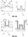
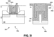
- Figures 3A-3I illustrate cross-sectional views are shown for respective stages 300-308 of processing to fabricate an IC device (configured to provide transistor functionality) having a multilayer high-k gate stack extending under a gate structure and over an existing semiconductor fin structure.
- Figures 3A-3I show respective median (y-z plane) cross-sectional views 300a-308a and respective transverse (x-z plane) cross-sectional views 300b-308b.
- Figure 3A shows the process after stage 300 in which a fin structure (such as the illustrative fin 310 shown) is formed extending through a trench which is formed at least in part by a trench dielectric 317.
- Fin 310 includes some or all of the features of fin structure 110, for example.
- fin 310 comprises one or more semiconductor materials and forms side surfaces including, for example, the illustrative side 312 shown.
- Side 312 has a vertical (z-axis) span "dz" which extends at least between a top of fin 310 and a horizontal surface, such as that of trench dielectric 317. In an example embodiment, such a vertical span is in a range of 10 nm to 200 nm. However, such dimensions may vary according to implementation-specific details, in different embodiments.
- the formation of fin 310 and trench dielectric 317 include operations that are adapted, for example, from conventional techniques for fabricating finFET transistors.
- Figure 3B shows the process after stage 301 in which a dielectric layer 320 is formed to extend, e.g., along the x-axis dimension shown - across and over at least a portion of fin 310.
- Dielectric layer 320 may correspond to underlayer gate dielectric 120, for example. At least a portion of dielectric layer 320 is to serve as a structure to promote electrical insulation in a transistor structure. At least a portion of dielectric layer 320 - e.g., a portion which is adjacent to, and conformal with, some of fin 310 - is to provide at least part of a gate dielectric structure.
- a material of the dielectric layer 320 comprises silicon and one of oxygen, nitrogen, or carbon - e.g., wherein the dielectric layer 320 material is one of silicon oxides (SiO 2 ), silicon oxynitrides (SiON), silicon nitrides (SiN), silicon carbonitrides (SiCN), carbon-doped oxide (SiOC), or combinations thereof.
- dielectric layer 320 includes any of a variety of suitable materials that are adapted from convention techniques for providing electrical insulation for non-planar transistors.
- an average thickness of the dielectric layer 320 is equal to or less than 40 Angstroms ( ⁇ ) thick - e.g., in a range of 5 ⁇ to 40 ⁇ and, in some embodiments, in a range of 5 ⁇ to 20 ⁇ .
- ⁇ Angstroms
- formation of the dielectric layer 320 includes any of a variety of additive processes (such as chemical vapor deposition, atomic layer deposition or the like) adapted, for example, from conventional semiconductor fabrication techniques.
- Figure 3C shows the process after stage 303 in which in order to form spacers that may correspond to spacers 150, 151, a dummy (i.e., sacrificial) gate 335 is first formed over a portion of fin 310.
- a portion of fin 310 under dummy gate 335 provides a channel region 113 ( Fig. 2 ) of a transistor structure (or other such IC device).
- Dummy gate 335 includes a layer of material such as polysilicon (e.g., doped, undoped, amorphous, crystalline or the like), or any of various suitable carbon or nitride based materials, for example.
- formation of dummy gate 335 includes forming a patterned resist or hard mask 337 on dielectric layer 320 and depositing a dummy gate material through the patterned resist mask. Any of a variety of known mask, patterning, deposition and/or etch methods and techniques can be used to form dummy gate 335, in various embodiments.
- Figure 3D shows the process after stage 304 in which etching and/or other subtractive processing is performed, e.g., with a patterned mask 337 to remove respective portions of dielectric layer 320 that is not under dummy gate 335. Such subtractive processing leaves portion 321 of dielectric layer 320 in this embodiment.
- Figure 3E shows the process after stage 305 in which spacers 350 and 351 are formed each at a respective opposite sidewall of dummy gate 335.
- Spacers 350 and 351 include features of insulation spacers 150 and 151 except where (for example) portions 321 abuts against, and does not extend under, spacer portions 350 and 351.
- Figure 3F shows the process after stage 306 in which doped source and drain regions 316 and 318 are formed in portions of fin 310 that are on opposite respective sides of channel region 113 ( Fig. 2 ).
- Other transistor structures formed by the additional fabrication include raised epitaxial (epi) source or drain regions 317 and 319 each extending over a respective one of the doped source or drain regions 316, 318 - source or drain contact structures (not shown), and/or the like.
- Such additional fabrication includes processes that, for example, are adapted from conventional mask, patterning, etching, deposition, doping, polishing, and/or other techniques.
- Figure 3G shows the process after stage 307 in which dummy gate 335 is etched or otherwise removed. Removal of dummy gate 335 exposes respective side surfaces 352 and 353 of spacers 350 and 351. In some embodiments, etching to remove dummy gate 335 also removes a dummy oxide (if any) which was previously deposited on layer 320. Note, layer 320 is subsequently removed and then reformed. In embodiments, the dummy oxide and reformed dummy oxide may comprise SiO 2 or SiON for example.
- Figure 3H shows the process after stage 308 in which a multilayer high-k gate dielectric stack 340 comprising at least a first high-k material 340A and a second high-k material 340B up to an n th high-k material 140N are sequentially formed.
- the first high-k material 340A extends across and over fin 310 in a region between spacers 350 and 351 such that the first high-k material 340A is adjacent and conformal to spacer sides 352 and 353 and dielectric layer 320.
- each successive high-k material is conformal to the previous high-k material.
- One or more treatments are performed to at least of the first high-k material layer such that one of the high-k materials has a modified property different from the other high-k materials, wherein the modified property comprises at least one of ferroelectricity, crystalline phase, strain, surface roughness, and lattice constant and combinations thereof.
- Formation of the multilayer high-k gate dielectric stack 340 comprises deposition of dielectric materials that have a higher dielectric constant than that of dielectric layer 320.
- the high-k materials used to form multilayer high-k gate dielectric stack 340 comprise oxygen and a metal which, for example, includes, but is not limited to, one or more of aluminum (Al), tantalum (Ta), hafnium (Hf), zirconium (Zr), lanthanum (La), titanium (Ti) magnesium (Mg) or manganese (Mn).
- the second dielectric material includes hafnium oxide, hafnium oxy-nitride, hafnium silicate, lanthanum oxide, zirconium oxide, zirconium silicate, tantalum oxide, barium strontium titanate, barium titanate, strontium titanate, yttrium oxide, aluminum oxide, lead scandium tantalum oxide, lead zinc niobate, or a combination thereof.
- the multilayer high-k gate dielectric stack 340 may be approximately 1 to 100 ⁇ in thickness.
- the various high-k material layers may be the same or different thicknesses, with a minimum thickness of. 5 ⁇ each.
- one high-k material layer may be 5 ⁇ , while the next is 1 nanometer, and the like.
- fabrication of one or more of layers 320, multilayer high-k gate dielectric stack 340, and/or spacers 350 and 351 comprise one or more operations which, for example, are adapted from conventional semiconductor fabrication techniques such as mask, lithography, deposition (e.g., chemical vapor deposition), etching and/or other processes. Some of these conventional techniques are not detailed herein to avoid obscuring certain features of various embodiments.
- Figure 3I shows the process after stage 309 in which a gate electrode structure 362 is formed on the multilayer high-k gate dielectric stack 340, e.g., using operations adapted from conventional metallization and/or other deposition techniques.
- an integrated circuit structure includes a multilayer high-k gate dielectric stack comprising at least a first high-k material and a second high-k material in combination with at least one low-k dielectric layer in a GAA (gate all around) architecture
- Figure 4B provides a cross-sectional illustration of the non-planar transistor 400 across the channel region 413 of the fin 410.
- the transistor 400 may be substantially similar to the transistor 100 described above with respect to Figures 1 and 2 , with the exception that the transistor depicted is a GAA transistor.
- the transistor 400 comprises a fin 410 extending from a substrate (not shown), the fin 410 comprises a hanging fin region, which includes a channel region 413, S/D regions 448 on opposite sides of the channel region 413, and a sub-fin 416 region under the channel region 413 between the S/D regions 448, where the channel region 413 and the sub-fin region 416 are spaced apart.
- a first isolation region 447 is adjacent both sides the sub-fin region 416 beneath a second isolation region 448.
- the second isolation region 448 includes a trench 449 in which the channel region 413 is located.
- a gate dielectric stack comprises a dummy oxide 431, a low-k material 402, a first high-k material 437, a second high-k material comprising a first portion 440-1 and a second portion 440-2, and a gate electrode 462 between gate spacers 438.
- the first high-k material 440-1 and the second high-k material 440-2 may comprise a multilayer high-k gate dielectric stack described above.
- the first high-k material 437 may comprise a single layer or layers 440A, 440B to 440N.
- the gate dielectric stack comprises the low-k material 402 conformal to a top surface of the first isolation region 447 and to sides and top of the channel region 413.
- the first high-k material 437 is conformal to the low-k material 402 over the first isolation region 447 and on sides and top of the channel region 413.
- the dummy oxide 431 is conformal to the first high-k material 437 over the first isolation region 447 and over the sides and top of the channel region 413.
- the first portion 440-1 of the second high-k material is over the first high-k material 437 on all four sides of the channel region 413, and the second portion 440-2 of the second high-k material is conformal to a top surface of the second isolation region 448, conformal to sides and bottom of the trench 449, and conformal to a top of the sub-fin region 416.
- the gate electrode 462 fills the trench 449 and surrounds a perimeter of the first portion 440-1 of the second high-k material over the channel region 413.
- Figure 4A shows a portion of the low-k material 402, the first portion 440-1 of the second high-k material, the gate electrode 462 and the second portion 440-2 of the second high-k material all below a bottommost surface of the channel region 413.
- the second isolation layer 448 e.g. an interlayer dielectric (ILD) surrounds the gate stack and is positioned over a top surface of the S/D regions 412.
- the low-k material 402 is shown conformal to the first isolation region 447
- the first high-k material 437 is shown conformal to the low-k material 402
- the dummy oxide 431 is shown conformal to first high-k material 437.
- the low-k material 402, the first high-k material 437 and the dummy oxide 431 each abut the second portion 440-2 of the second high-k material at the bottom of the trench 449.
- a transistor architecture comprising a hanging fin channel region spaced apart from a sub-fin region and a multilayer gate dielectric comprising a low-k material and two high-k materials may overcome the limit of inversion charge of conventional gate oxides by utilizing SOI template formation while maintaining the capability of multilayer high-k, and thus enabling high-performing and low-leakage transistors.
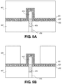
- Figures 5A-5F illustrate cross-sectional fin cut views of a process for fabricating an IC device (configured to provide transistor functionality) having a hanging fin channel region spaced apart from a sub-fin region and a multilayer gate dielectric comprising a low-k material and a high-k material.
- Figure 5A illustrates the fabrication process after formation of a channel region 413 over a sub-fin region 416 of a fin, where a first isolation region 447 is on either side of the sub-fin.
- the sub-fin region 416 further includes a top sacrificial layer 403, such as Si x Ge 1-x .
- a gate dielectric stack comprising the low-k material 402 is formed conformal to a top surface of the first isolation region 447 and sides and top of the channel region 413.
- the first high-k material 437 is formed conformal to the low-k material 402, and the dummy oxide 431 is formed conformal to the first high-k material 437.
- a dummy gate 401 (e.g., a-Si or p-Si) is formed over the fin and the gate dielectric stack.
- Figure 5B illustrates the fabrication process during a dummy gate replacement process is performed in which the dummy gate 401 is first removed and then replaced by forming a second isolation region 448 over the top of the gate dielectric stack.
- the second isolation region 448 is etched to form a trench on each side and over a top the channel region 413.
- the width of the channel region 413 may range from 10 to 100 nm and the width of the low-k material 402 may range from 3 to 50 nm.
- Figure 5C illustrates the fabrication process after a sacrificial material 404 is deposited in the trench over the gate dielectric stack on either side of the fin, and a non-conformal sacrificial material 406 is deposited over a top and sidewalls of the second isolation region 448 and over a top and sidewalls of the gate dielectric on the channel region 413.
- the non-conformal sacrificial material 406 is formed with thicker horizontal portions than vertical portions on the sidewalls.
- Figure 5D illustrates the fabrication process after the sacrificial material 404 and the non-conformal sacrificial material 406 are removed from over the gate dielectric stack at the bottom of the trench, but not from the channel region 413. Portions of the gate dielectric stack beneath the sacrificial material 404 and under the channel region 413 are also removed by etching along with the sacrificial layer 403 from the sub-fin region 416. The removal of these materials leaves a cavity 407 between hanging channel region and the sub-fin region.
- Figure 5E illustrates the fabrication process after removal of the non-conformal sacrificial material 406 and the dummy oxide 431 from the top and sides of the channel region 413.
- a top of the sub-fin region 416 is oxidized to form/grow low-k material (e.g., an oxide) 402.
- an ALD process could be used.
- the low-k material on the sub-fin region 416 may be the same or different than the low-k material over the first isolation regions 447 and the channel region 413.
- the presence of the low-k material 402 helps prevent the high-k material from touching the channel material to reduce high-k scattering and to preserve mobility of the channel material.
- Figure 5F illustrates the fabrication process after the second high-k material 440-2 is formed conformal to tops and sides of the second isolation region 448 and a bottom of the cavity 407; and after the first high-k material 440-1 is formed conformal to all four sides of the channel region 413.
- the final stage of the fabrication process is shown after the gate electrode 462 is formed in the trench in the second isolation region 448 and in the cavity 407 of the channel region 413 for four sided gate control.
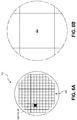
- FIGS. 6A and 6B are top views of a wafer and dies that include one or more multilayer high-k gate dielectrics, in accordance with one or more of the embodiments disclosed herein.
- a wafer 600 may be composed of semiconductor material and may include one or more dies 602 having integrated circuit (IC) structures formed on a surface of the wafer 600.
- IC integrated circuit
- Each of the dies 602 may be a repeating unit of a semiconductor product that includes any suitable IC (e.g., ICs including one or more multilayer high-k gate dielectrics, such as described above.
- the wafer 600 may undergo a singulation process in which each of the dies 602 is separated from one another to provide discrete "chips" of the semiconductor product.
- structures that include embedded non-volatile memory structures having an independently scaled selector as disclosed herein may take the form of the wafer 600 (e.g., not singulated) or the form of the die 602 (e.g., singulated).
- the die 602 may include one or more embedded non-volatile memory structures based independently scaled selectors and/or supporting circuitry to route electrical signals, as well as any other IC components.
- the wafer 600 or the die 602 may include an additional memory device (e.g., a static random access memory (SRAM) device), a logic device (e.g., an AND, OR, NAND, or NOR gate), or any other suitable circuit element. Multiple ones of these devices may be combined on a single die 602.
- a memory array formed by multiple memory devices may be formed on a same die 602 as a processing device or other logic that is configured to store information in the memory devices or execute instructions stored in the memory array.
- Embodiments disclosed herein may be used to manufacture a wide variety of different types of integrated circuits and/or microelectronic devices. Examples of such integrated circuits include, but are not limited to, processors, chipset components, graphics processors, digital signal processors, micro-controllers, and the like. In other embodiments, semiconductor memory may be manufactured. Moreover, the integrated circuits or other microelectronic devices may be used in a wide variety of electronic devices known in the arts. For example, in computer systems (e.g., desktop, laptop, server), cellular phones, personal electronics, etc. The integrated circuits may be coupled with a bus and other components in the systems. For example, a processor may be coupled by one or more buses to a memory, a chipset, etc. Each of the processor, the memory, and the chipset, may potentially be manufactured using the approaches disclosed herein.
- FIG. 7 illustrates a block diagram of an electronic system 700, in accordance with an embodiment of the present disclosure.
- the electronic system 700 can correspond to, for example, a portable system, a computer system, a process control system, or any other system that utilizes a processor and an associated memory.
- the electronic system 700 may include a microprocessor 702 (having a processor 704 and control unit 706), a memory device 708, and an input/output device 710 (it is to be appreciated that the electronic system 700 may have a plurality of processors, control units, memory device units and/or input/output devices in various embodiments).
- the electronic system 700 has a set of instructions that define operations which are to be performed on data by the processor 704, as well as, other transactions between the processor 704, the memory device 708, and the input/output device 710.
- the control unit 706 coordinates the operations of the processor 704, the memory device 708 and the input/output device 710 by cycling through a set of operations that cause instructions to be retrieved from the memory device 708 and executed.
- the memory device 708 can include a non-volatile memory cell as described in the present description.
- the memory device 708 is embedded in the microprocessor 702, as depicted in Figure 7 .
- the processor 704, or another component of electronic system 700 includes one or more multilayer high-k gate dielectrics, such as those described herein.
- Figure 8 is a cross-sectional side view of an integrated circuit (IC) device assembly that may include one or more multilayer high-k gate dielectrics, in accordance with one or more of the embodiments disclosed herein.
- IC integrated circuit
- an IC device assembly 800 includes components having one or more integrated circuit structures described herein.
- the IC device assembly 800 includes a number of components disposed on a circuit board 802 (which may be, e.g., a motherboard).
- the IC device assembly 800 includes components disposed on a first face 840 of the circuit board 802 and an opposing second face 842 of the circuit board 802.
- components may be disposed on one or both faces 840 and 842.
- any suitable ones of the components of the IC device assembly 800 may include a number of a multilayer high-k gate dielectric, such as disclosed herein.
- the circuit board 802 may be a printed circuit board (PCB) including multiple metal layers separated from one another by layers of dielectric material and interconnected by electrically conductive vias. Any one or more of the metal layers may be formed in a desired circuit pattern to route electrical signals (optionally in conjunction with other metal layers) between the components coupled to the circuit board 802.
- the circuit board 802 may be a non-PCB substrate.
- the IC device assembly 800 illustrated in Figure 8 includes a package-on-interposer structure 836 coupled to the first face 840 of the circuit board 802 by coupling components 816.
- the coupling components 816 may electrically and mechanically couple the package-on-interposer structure 836 to the circuit board 802, and may include solder balls (as shown in Figure 8 ), male and female portions of a socket, an adhesive, an underfill material, and/or any other suitable electrical and/or mechanical coupling structure.
- the package-on-interposer structure 836 may include an IC package 820 coupled to an interposer 804 by coupling components 818.
- the coupling components 818 may take any suitable form for the application, such as the forms discussed above with reference to the coupling components 816. Although a single IC package 820 is shown in Figure 8 , multiple IC packages may be coupled to the interposer 804. It is to be appreciated that additional interposers may be coupled to the interposer 804.
- the interposer 804 may provide an intervening substrate used to bridge the circuit board 802 and the IC package 820.
- the IC package 820 may be or include, for example, a die (the die 702 of Figure 7B ), or any other suitable component.
- the interposer 804 may spread a connection to a wider pitch or reroute a connection to a different connection.
- the interposer 804 may couple the IC package 820 (e.g., a die) to a ball grid array (BGA) of the coupling components 816 for coupling to the circuit board 802.
- BGA ball grid array
- the IC package 820 and the circuit board 802 are attached to opposing sides of the interposer 804.
- the IC package 820 and the circuit board 802 may be attached to a same side of the interposer 804.
- three or more components may be interconnected by way of the interposer 804.
- the interposer 804 may be formed of an epoxy resin, a fiberglass-reinforced epoxy resin, a ceramic material, or a polymer material such as polyimide. In some implementations, the interposer 804 may be formed of alternate rigid or flexible materials that may include the same materials described above for use in a semiconductor substrate, such as silicon, germanium, and other group III-V and group IV materials.
- the interposer 804 may include metal interconnects 810 and vias 808, including but not limited to through-silicon vias (TSVs) 806.
- TSVs through-silicon vias
- the interposer 804 may further include embedded devices, including both passive and active devices.
- Such devices may include, but are not limited to, capacitors, decoupling capacitors, resistors, inductors, fuses, diodes, transformers, sensors, electrostatic discharge (ESD) devices, and memory devices. More complex devices such as radio-frequency (RF) devices, power amplifiers, power management devices, antennas, arrays, sensors, and microelectromechanical systems (MEMS) devices may also be formed on the interposer 804.
- RF radio-frequency
- MEMS microelectromechanical systems
- the package-on-interposer structure 836 may take the form of any of the package-on-interposer structures known in the art.
- the IC device assembly 800 may include an IC package 824 coupled to the first face 840 of the circuit board 802 by coupling components 822.
- the coupling components 822 may take the form of any of the embodiments discussed above with reference to the coupling components 816
- the IC package 824 may take the form of any of the embodiments discussed above with reference to the IC package 820.
- the IC device assembly 800 illustrated in Figure 8 includes a package-on-package structure 834 coupled to the second face 842 of the circuit board 802 by coupling components 828.
- the package-on-package structure 834 may include an IC package 826 and an IC package 832 coupled together by coupling components 830 such that the IC package 826 is disposed between the circuit board 802 and the IC package 832.
- the coupling components 828 and 830 may take the form of any of the embodiments of the coupling components 816 discussed above, and the IC packages 826 and 832 may take the form of any of the embodiments of the IC package 820 discussed above.
- the package-on-package structure 834 may be configured in accordance with any of the package-on-package structures known in the art.
- FIG. 9 illustrates a computing device 900 in accordance with one implementation of the disclosure.
- the computing device 900 houses a board 902.
- the board 902 may include a number of components, including but not limited to a processor 904 and at least one communication chip 906.
- the processor 904 is physically and electrically coupled to the board 902.
- the at least one communication chip 906 is also physically and electrically coupled to the board 902.
- the communication chip 906 is part of the processor 904.
- computing device 900 may include other components that may or may not be physically and electrically coupled to the board 902. These other components include, but are not limited to, volatile memory (e.g., DRAM), non-volatile memory (e.g., ROM), flash memory, a graphics processor, a digital signal processor, a crypto processor, a chipset, an antenna, a display, a touchscreen display, a touchscreen controller, a battery, an audio codec, a video codec, a power amplifier, a global positioning system (GPS) device, a compass, an accelerometer, a gyroscope, a speaker, a camera, and a mass storage device (such as hard disk drive, compact disk (CD), digital versatile disk (DVD), and so forth).
- volatile memory e.g., DRAM
- non-volatile memory e.g., ROM
- flash memory e.g., a graphics processor, a digital signal processor, a crypto processor, a chipset, an antenna,
- the communication chip 906 enables wireless communications for the transfer of data to and from the computing device 900.
- wireless and its derivatives may be used to describe circuits, devices, systems, methods, techniques, communications channels, etc., that may communicate data through the use of modulated electromagnetic radiation through a non-solid medium. The term does not imply that the associated devices do not contain any wires, although in some embodiments they might not.
- the communication chip 906 may implement any of a number of wireless standards or protocols, including but not limited to Wi-Fi (IEEE 802.11 family), WiMAX (IEEE 802.16 family), IEEE 802.20, long term evolution (LTE), Ev-DO, HSPA+, HSDPA+, HSUPA+, EDGE, GSM, GPRS, CDMA, TDMA, DECT, Bluetooth, derivatives thereof, as well as any other wireless protocols that are designated as 3G, 4G, 5G, and beyond.
- the computing device 900 may include a plurality of communication chips 906.
- a first communication chip 906 may be dedicated to shorter range wireless communications such as Wi-Fi and Bluetooth and a second communication chip 906 may be dedicated to longer range wireless communications such as GPS, EDGE, GPRS, CDMA, WiMAX, LTE, Ev-DO, and others.
- the processor 904 of the computing device 900 includes an integrated circuit die packaged within the processor 904.
- the integrated circuit die of the processor includes one or more multilayer high-k gate dielectrics, in accordance with implementations of embodiments of the disclosure.
- the term "processor" may refer to any device or portion of a device that processes electronic data from registers and/or memory to transform that electronic data into other electronic data that may be stored in registers and/or memory.
- the communication chip 906 also includes an integrated circuit die packaged within the communication chip 906.
- the integrated circuit die of the communication chip 906 includes one or more multilayer high-k gate dielectrics, in accordance with implementations of embodiments of the disclosure.
- another component housed within the computing device 900 may contain an integrated circuit die that includes one or more multilayer high-k gate dielectrics, in accordance with implementations of embodiments of the disclosure.
- the computing device 900 may be a laptop, a netbook, a notebook, an ultrabook, a smartphone, a tablet, a personal digital assistant (PDA), an ultra mobile PC, a mobile phone, a desktop computer, a server, a printer, a scanner, a monitor, a set-top box, an entertainment control unit, a digital camera, a portable music player, or a digital video recorder.
- the computing device 900 may be any other electronic device that processes data.
- embodiments described herein include a multilayer high-k gate dielectric.
Landscapes
- Insulated Gate Type Field-Effect Transistor (AREA)
- Metal-Oxide And Bipolar Metal-Oxide Semiconductor Integrated Circuits (AREA)
- Thin Film Transistor (AREA)
Abstract
Description
- Embodiments of the disclosure are in the field of integrated circuit structures and, in particular, a multilayer high-k gate dielectric for a high performance logic transistor.
- For the past several decades, the scaling of features in integrated circuits has been a driving force behind an ever-growing semiconductor industry. Scaling to smaller and smaller features enables increased densities of functional units on the limited real estate of semiconductor chips. For example, shrinking transistor size allows for the incorporation of an increased number of memory or logic devices on a chip, lending to the fabrication of products with increased capacity. The drive for ever-more capacity, however, is not without issue. The necessity to optimize the performance of each device becomes increasingly significant.
- Variability in conventional and state-of-the-art fabrication processes may limit the possibility to further extend them into the sub-10 nm range. Consequently, fabrication of the functional components needed for future technology nodes may require the introduction of new methodologies or the integration of new technologies in current fabrication processes or in place of current fabrication processes.
- For example, in a FinFET, a type of non-planar transistor built around a thin strip of semiconductor material referred to as a fin, a gate oxide is a dielectric/insulating layer that separates the gate terminal of the transistor from the underlying source and drain terminals. An inversion layer is formed in the semiconductor substrate via capacitive coupling when a gate bias is applied. The inversion layer provides a channel through which current can pass between source and drain terminals. Conventional gate oxide scaling has limits that may also limit the inversion charge while meeting all the requirement in the reliability.
-
-
Figure 1 shows one example of a portion of an IC device consistent with the present disclosure, in this case a portion of a FinFET. -
Figure 2 shows a view of a cross-section X-X' ofIC device 100. -
Figures 3A-3I illustrate cross-sectional views are shown for respective of processing to fabricate an IC device (configured to provide transistor functionality) having a multilayer high-k gate stack extending under a gate structure and over an existing semiconductor fin structure. -
Figures 4A and 4B illustrate a pair of cross-sectional illustrations of a non-planar transistor is shown, in accordance with an embodiment. -
Figures 5A-5F illustrate cross-sectional fin cut views of a process for fabricating an IC device (configured to provide transistor functionality) having a hanging fin channel region spaced apart from a sub-fin region and a multilayer gate dielectric comprising a low-k material and a high-k material. -
Figures 6A and 6B are top views of a wafer and dies that include one or more multilayer high-k gate dielectrics, in accordance with one or more of the embodiments disclosed herein. -
Figure 7 illustrates a block diagram of an electronic system, in accordance with an embodiment of the present disclosure. -
Figure 8 is a cross-sectional side view of an integrated circuit (IC) device assembly that may include one or more multilayer high-k gate dielectrics, in accordance with one or more of the embodiments disclosed herein. -
Figure 9 illustrates a computing device in accordance with one implementation of the disclosure. - A multilayer high-k gate dielectric for a high performance logic transistor are described. In the following description, numerous specific details are set forth, such as specific material and tooling regimes, in order to provide a thorough understanding of embodiments of the present disclosure. It will be apparent to one skilled in the art that embodiments of the present disclosure may be practiced without these specific details. In other instances, well-known features, such as single or dual damascene processing, are not described in detail in order to not unnecessarily obscure embodiments of the present disclosure. Furthermore, it is to be understood that the various embodiments shown in the Figures are illustrative representations and are not necessarily drawn to scale. In some cases, various operations will be described as multiple discrete operations, in turn, in a manner that is most helpful in understanding the present disclosure, however, the order of description should not be construed to imply that these operations are necessarily order dependent. In particular, these operations need not be performed in the order of presentation.
- Certain terminology may also be used in the following description for the purpose of reference only, and thus are not intended to be limiting. For example, terms such as "upper", "lower", "above", "below," "bottom," and "top" refer to directions in the drawings to which reference is made. Terms such as "front", "back", "rear", and "side" describe the orientation and/or location of portions of the component within a consistent but arbitrary frame of reference which is made clear by reference to the text and the associated drawings describing the component under discussion. Such terminology may include the words specifically mentioned above, derivatives thereof, and words of similar import.
- One or more embodiments described herein are directed to structures and architectures for fabricating a multilayer high-k gate dielectric for a high performance logic transistor, such as a FinFET or gate-all-around FET. One or more embodiments described herein are further directed to structures and architectures for fabricating an integrated circuit that utilizes SOI template formation while maintaining the capability of multi-layer high k, enabling high performing & low-leakage transistors. Embodiments may include or pertain to one or more of transistors, semiconducting oxide materials, and system-on-chip (SoC) technologies of future technology nodes.
- To provide context, a FinFET is one type of non-planar transistor which is built around a thin strip of semiconductor material (referred to as the "fin"). The transistor includes the standard field effect transistor (FET) nodes/components: a gate, a gate dielectric, a source region, and a drain region. During operation, a conductive channel of the device resides on the outer sides of the fin beneath the gate dielectric. Specifically, current runs along "sidewalls" of the fin as well as along the top side of the fin. Because the conductive channel essentially resides along the three different outer, planar regions of the fin, such a FinFET is typically referred to as a "tri-gate" FinFET. Other types of FinFETs exist (such as "double-gate" FinFETs in which the conductive channel principally resides only along both sidewalls of the fin and not along the top side of the fin).
- Typically, fabricating a non-planar transistor includes depositing a dielectric material into a given space to form a gate dielectric or oxide to provide at least some electrical insulation between two adjoining structures, e.g., a fin and a gate. A common material for a gate dielectric is silicon dioxide, which has a dielectric constant around 3.8. However, as improvements to semiconductor fabrication processing continue to reduce the size of transistor structures, limits are placed on gate oxide thickness scaling. As a result, there is expected to be a growing premium placed on incremental improvements to techniques for overcoming the limits of gate oxide thickness scaling and the inversion charge of a conventional gate oxide, while maintaining low gate leakage.
- In accordance with a first aspect of the disclosed embodiments, a non-planar transistor is fabricated with a multilayer oxide using high-k gate materials and an amorphous layer and/or a crystalline layer, thus enabling a higher inversion charge. In accordance with a second aspect of the disclosed embodiments, a non-planar transistor is fabricated with a buried high-k material combined with a pseudo-SOI template. Non-planar transistors fabricated using such architectures may exhibit an increase in gate control, stability, and performance of thin film transistors. Applications of such systems may include, but are not limited to, back end (BEOL) logic, memory, or analog applications. Embodiments described herein may include non-planar structures that effectively increase gate oxide thickness scaling and inversion charge by integrating a multilayer gate dielectric in unique architectures. In one embodiment, high-k materials are used for the gate dielectric, where the high-k materials have a dielectric constant k greater than 7. In one embodiment, the non-planar transistor may comprise any type of multi-gate, nanowire, or nanoribbon device.
- Referring now to the first aspect of the disclosed embodiments, an integrated circuit structure provides a multilayer high-k gate dielectric stack comprising at least a first high-k material and a second high-k material. The first high-k material extends conformally over a fin over a channel region, while the second high-k material is conformal to the first high-k material, wherein either the first high-k material or the second high-k material has a modified material property different from the other high-k material, where the modified material property comprises at least one of ferroelectricity, crystalline phase, texturing, ordering orientation of the crystalline phase or texturing to a specific crystalline direction or plane, strain, surface roughness, and lattice constant and combinations thereof. A metal gate material is over and on a top most high-k material of the multilayer high-k gate dielectric stack. In embodiments, the modified material property may include different crystalline phases, including crystalline, poly crystalline, nanocrystalline, and amorphous. In embodiments, the modified strained property may originate from an annealing process or other heat treatment, and extra sequences of sacrificial material deposition and etching, which alters the physical and sometimes chemical properties of a material.
-
Figure 1 shows one example of a portion of anIC device 100 consistent with the present disclosure, in this case a portion of a FinFET. As shown,IC device 100 includes asubstrate 101, a trench dielectric 102 onsubstrate 101, and afin structure 110 disposed in a trench which is formed by trench dielectric 102.Fin structure 110 comprises, for example, atop surface 114 and a pair of laterally opposite sidewalls (sidewall 111 andopposing sidewall 112, respectively). In some embodiments, portions offin structure 110 which are vertically offset from one another comprise different respective group III-V (and/or other) semiconductor materials. -
Substrate 101 is formed of any of a variety of materials that are suitable for use as a substrate of a semiconductor device, and in particular as a substrate for non-planar transistors such as FinFETS and multi-gate transistors. Non-limiting examples of such suitable materials include silicon (Si), germanium (Ge), silicon-germanium (SiGe), silicon-carbide (SiC), sapphire, a group III-V semiconductor, a silicon on insulate (SOI) substrate, combinations thereof, and the like. Without limitation, in someembodiments substrate 101 is formed from or includes single crystal silicon. - In some embodiments the non-planar semiconductor device includes at least one trench that is formed on or within the substrate. In the embodiment of
IC device 100, a trench (not separately labeled) is defined by the sidewalls of trench dielectric 102 (hereinafter, trench sidewalls) and an upper portion ofsubstrate 101. The trench thus includes at least two opposing sides (trench sidewalls) and a bottom. A bottom of the trench is formed at least in part by an upper surface of the substrate, and/or one or more buffer and/or transition layers deposited on the substrate. A trench of any of a variety of suitable dimensions may be used, in different embodiments, according to implementation-specific details. Without limitation, in some embodiments the height (z-axis dimension) and width (y-axis dimension) of the trench enables the deposition of the materials used to form fin structure 110 - e.g., via an aspect ratio trapping (ART) process. Accordingly, in some embodiments the width of the trench is in a range of 1 nanometers (nm) to 500 nanometers (nm), such as in a range of 1 nm to 300 nm, in a range of 1 nm to 100 nm, in a range of 5 nm to 100 nm, or even in a range of 5 nm to 30 nm. Likewise, the height of such a trench is range, for example, in a range of 1 nm to 500 nm, such as a range of 100 nm to 300 nm. - Trench dielectric 102, which may also comprise multiple layers, is formed from any of a variety of materials that are suitable for use as a trench dielectric material of a non-planar semiconductor device. Non-limiting examples of such materials include oxides, nitrides and alloys, such as but not limited to silicon oxide (SiO2), silicon nitride (SiN), silicon oxycarbide (SiCO), silicon carbon oxynitride (SiCON), silicon carbonitride (SiCN), combinations thereof, and the like.
-
Figure 2 shows a view of a cross-section X-X' ofIC device 100. A non-planar transistor ofIC device 100 comprises structures which are variously disposed in or onfin structure 110. For example, such a non-planar transistor may include achannel structure 113, two doped source or drain ("SD")structures channel structure 113, and raised epitaxial (epi) source or drainregions - According to the first aspect of the disclosed embodiments, a gate structure of the non-planar transistor comprises
gate electrode 162 and a multilayer high-k gatedielectric stack 140 comprising at least a first high-k material 140A and a second high-k material 140B up to an nth high-k material 140N. A gate electrode162 is over and on a topmost high-k material in the multilayer high-k gatedielectric stack 140. More particularly,gate electrode 162 extends over and across a portion offin 110 in a region betweeninsulation spacers IC device 100. - According to the first aspect of the present embodiment, either the first high-
k material 140A or the second high-k material 140B has a modified material property different from the other high-k material, wherein the modified property comprises at least one of ferroelectricity, crystalline phase, texturing, ordering orientation of the crystalline phase or texturing to a specific crystalline direction or plane, strain, surface roughness, and lattice constant and combinations thereof. In embodiments, the crystalline phases, include crystalline, polycrystalline, nanocrystalline, and amorphous. For example, the second high-k material 140B comprises the same or different material as the first high-k material 140A, but the second high-k material 140B may have a different crystalline phase, strain, surface roughness, and/or lattice constant than the first high-k material 140A. A channel treatment may be employed to modify one or more properties of one or more of the high-k materials 140A to 140N. For example, annealing or surface texturing or an extra sequence of sacrificial material deposition and etching may be used to modify the strain of one or more of the high-k materials 140A to 140N. - In an embodiment, operation of
IC device 100 includes selectively controlling a current between source or drainregions channel region 113, by applying a voltage togate electrode 162. This functionality is enabled in part by dielectric structures which provide electrical insulation betweengate electrode 162 andchannel region 113. Due to the interaction between the high-k materials 140A to 140N having different modified properties, the transistor provides a higher current. For example, different materials and dopants, or doping profile, material profile, strain and templating of each layer provides different growth characteristics in each distinct layer and in the whole stack, enabling higher inversion charge through the whole multilayer high-k gatedielectric stack 140. The result is a higher charge may be introduced into thechannel 113 and higher current may be achieved for the transistor for higher performance. - In some embodiments,
gate electrode 162 includes a metal with a work function below 5 eV. Themetal gate electrode 162 includes, for example, an elemental metal layer, a metal alloy layer, or laminate structure of either or both. In some embodiments thegate electrode 162 may comprise a metal nitride, such as TiN (e.g., 4.0-4.7 eV). Thegate electrode 162 may also comprise Al (e.g., TiAIN). Other alloy constituents may also be employed, such as, but not limited to C, Ta, W, Pt, and Zn. - In one embodiment, the multilayer high-k gate
dielectric stack 140 may optionally include an optionalunderlayer gate dielectric 120 that extends conformally over the fin over the channel region under the multilayer high-k gate dielectric stack. In one embodiment, theunderlayer gate dielectric 120 has a dielectric constant less than the dielectric constant of the materials comprising the multilayer high-k gatedielectric stack 140. Theunderlayer gate dielectric 120 and the multilayer high-k gatedielectric stack 140 provide electrical insulation betweengate electrode 162 and each of a top of the channel structure and opposite vertical sidewalls of the channel structure. The presence ofunderlayer gate dielectric 120, however, may preserve channel mobility by mitigating scattering from higher k material resulting from the use of higher-k materials as gate dielectrics. - In the example embodiment shown, the
underlayer dielectric 120 adjoins, and is conformal to, respective portions of thefin 110sidewalls top surface 114. In one embodiment, theunderlayer dielectric 120 extends past the boundaries of thespacers underlayer dielectric 120 is present on thefin 110 only within the boundaries of thespacers - The multilayer high-k gate
dielectric stack 140 comprises at least two high-k material layers. The first high-k material 140A extends conformally over the fin over the channel region (and over theunderlayer gate dielectric 120 if present), the second high-k material 140B is conformal to the first high-k material 140A, the next high-k material is conformal to the second high-k material 140B, and so on. Thus, the multilayer high-k gatedielectric stack 140 includes portions that variously extend each betweengate electrode 162, a top ofunderlayer dielectric 120, and respective inner sidewalls ofinsulation spacers underlayer dielectric 120 is not conformal to the sides ofinsulation spacer - Generally, a method for fabricating an IC device configured with transistor functionality may include forming a fin that extends up from a substrate, the fin comprising source and drain regions, and a channel region between the source and drain regions. A multilayer high-k gate dielectric stack is formed comprising at least a first high-k material and a second high-k material, the first high-k material extending conformally over the fin over the channel region, and the second high-k material conformal to the first high-k material, wherein either the first high-k material or the second high-k material has a modified property different from the other high-k material. In embodiments, the modified property comprises at least one of crystalline phase, strain, surface roughness, and lattice constant. A gate electrode is formed over and on a topmost high-k material in the multilayer high-k gate dielectric stack. Any of a variety of additional or alternative structures may be fabricated in different embodiments.
-
Figures 3A-3I illustrate cross-sectional views are shown for respective stages 300-308 of processing to fabricate an IC device (configured to provide transistor functionality) having a multilayer high-k gate stack extending under a gate structure and over an existing semiconductor fin structure. For each of stages 300-308,Figures 3A-3I show respective median (y-z plane)cross-sectional views 300a-308a and respective transverse (x-z plane)cross-sectional views 300b-308b. -
Figure 3A shows the process afterstage 300 in which a fin structure (such as theillustrative fin 310 shown) is formed extending through a trench which is formed at least in part by atrench dielectric 317.Fin 310 includes some or all of the features offin structure 110, for example. In an embodiment,fin 310 comprises one or more semiconductor materials and forms side surfaces including, for example, theillustrative side 312 shown.Side 312 has a vertical (z-axis) span "dz" which extends at least between a top offin 310 and a horizontal surface, such as that oftrench dielectric 317. In an example embodiment, such a vertical span is in a range of 10 nm to 200 nm. However, such dimensions may vary according to implementation-specific details, in different embodiments. The formation offin 310 and trench dielectric 317 include operations that are adapted, for example, from conventional techniques for fabricating finFET transistors. -
Figure 3B shows the process afterstage 301 in which adielectric layer 320 is formed to extend, e.g., along the x-axis dimension shown - across and over at least a portion offin 310.Dielectric layer 320 may correspond tounderlayer gate dielectric 120, for example. At least a portion ofdielectric layer 320 is to serve as a structure to promote electrical insulation in a transistor structure. At least a portion of dielectric layer 320 - e.g., a portion which is adjacent to, and conformal with, some of fin 310 - is to provide at least part of a gate dielectric structure. By way of illustration and not limitation, a material of thedielectric layer 320 comprises silicon and one of oxygen, nitrogen, or carbon - e.g., wherein thedielectric layer 320 material is one of silicon oxides (SiO2), silicon oxynitrides (SiON), silicon nitrides (SiN), silicon carbonitrides (SiCN), carbon-doped oxide (SiOC), or combinations thereof. However, in other embodiments,dielectric layer 320 includes any of a variety of suitable materials that are adapted from convention techniques for providing electrical insulation for non-planar transistors. In some embodiments, an average thickness of thedielectric layer 320 is equal to or less than 40 Angstroms (Å) thick - e.g., in a range of 5 Å to 40 Å and, in some embodiments, in a range of 5 Å to 20 Å. However, such dimensions may vary according to implementation-specific details, in different embodiments. In an embodiment, formation of thedielectric layer 320 includes any of a variety of additive processes (such as chemical vapor deposition, atomic layer deposition or the like) adapted, for example, from conventional semiconductor fabrication techniques. -
Figure 3C shows the process afterstage 303 in which in order to form spacers that may correspond tospacers gate 335 is first formed over a portion offin 310. A portion offin 310 underdummy gate 335 provides a channel region 113 (Fig. 2 ) of a transistor structure (or other such IC device).Dummy gate 335 includes a layer of material such as polysilicon (e.g., doped, undoped, amorphous, crystalline or the like), or any of various suitable carbon or nitride based materials, for example. In an example embodiment, formation ofdummy gate 335 includes forming a patterned resist orhard mask 337 ondielectric layer 320 and depositing a dummy gate material through the patterned resist mask. Any of a variety of known mask, patterning, deposition and/or etch methods and techniques can be used to formdummy gate 335, in various embodiments. -
Figure 3D shows the process afterstage 304 in which etching and/or other subtractive processing is performed, e.g., with apatterned mask 337 to remove respective portions ofdielectric layer 320 that is not underdummy gate 335. Such subtractive processing leavesportion 321 ofdielectric layer 320 in this embodiment. -
Figure 3E shows the process afterstage 305 in which spacers 350 and 351 are formed each at a respective opposite sidewall ofdummy gate 335.Spacers insulation spacers portions 321 abuts against, and does not extend under,spacer portions -
Figure 3F shows the process afterstage 306 in which doped source and drainregions fin 310 that are on opposite respective sides of channel region 113 (Fig. 2 ). Other transistor structures formed by the additional fabrication include raised epitaxial (epi) source or drainregions regions 316, 318 - source or drain contact structures (not shown), and/or the like. Such additional fabrication includes processes that, for example, are adapted from conventional mask, patterning, etching, deposition, doping, polishing, and/or other techniques. -
Figure 3G shows the process afterstage 307 in whichdummy gate 335 is etched or otherwise removed. Removal ofdummy gate 335 exposes respective side surfaces 352 and 353 ofspacers dummy gate 335 also removes a dummy oxide (if any) which was previously deposited onlayer 320. Note,layer 320 is subsequently removed and then reformed. In embodiments, the dummy oxide and reformed dummy oxide may comprise SiO2 or SiON for example. -
Figure 3H shows the process afterstage 308 in which a multilayer high-k gatedielectric stack 340 comprising at least a first high-k material 340A and a second high-k material 340B up to an nth high-k material 140N are sequentially formed. The first high-k material 340A extends across and overfin 310 in a region betweenspacers k material 340A is adjacent and conformal to spacersides dielectric layer 320. After first high-k material 340A is formed, each successive high-k material is conformal to the previous high-k material. One or more treatments (not shown) are performed to at least of the first high-k material layer such that one of the high-k materials has a modified property different from the other high-k materials, wherein the modified property comprises at least one of ferroelectricity, crystalline phase, strain, surface roughness, and lattice constant and combinations thereof. - Formation of the multilayer high-k gate
dielectric stack 340 comprises deposition of dielectric materials that have a higher dielectric constant than that ofdielectric layer 320. In embodiments, the high-k materials used to form multilayer high-k gatedielectric stack 340 comprise oxygen and a metal which, for example, includes, but is not limited to, one or more of aluminum (Al), tantalum (Ta), hafnium (Hf), zirconium (Zr), lanthanum (La), titanium (Ti) magnesium (Mg) or manganese (Mn). For example, in some embodiments, the second dielectric material includes hafnium oxide, hafnium oxy-nitride, hafnium silicate, lanthanum oxide, zirconium oxide, zirconium silicate, tantalum oxide, barium strontium titanate, barium titanate, strontium titanate, yttrium oxide, aluminum oxide, lead scandium tantalum oxide, lead zinc niobate, or a combination thereof. - In various embodiments, the multilayer high-k gate
dielectric stack 340 may be approximately 1 to 100 Å in thickness. The various high-k material layers may be the same or different thicknesses, with a minimum thickness of. 5 Å each. For example, one high-k material layer may be 5 Å, while the next is 1 nanometer, and the like. - In some embodiments, fabrication of one or more of
layers 320, multilayer high-k gatedielectric stack 340, and/orspacers -
Figure 3I shows the process afterstage 309 in which agate electrode structure 362 is formed on the multilayer high-k gatedielectric stack 340, e.g., using operations adapted from conventional metallization and/or other deposition techniques. - Referring now to the second aspect of the disclosed embodiments, an integrated circuit structure includes a multilayer high-k gate dielectric stack comprising at least a first high-k material and a second high-k material in combination with at least one low-k dielectric layer in a GAA (gate all around) architecture, and
Figure 4B provides a cross-sectional illustration of thenon-planar transistor 400 across thechannel region 413 of thefin 410. In an embodiment, thetransistor 400 may be substantially similar to thetransistor 100 described above with respect toFigures 1 and 2 , with the exception that the transistor depicted is a GAA transistor. - In this embodiment, the
transistor 400 comprises afin 410 extending from a substrate (not shown), thefin 410 comprises a hanging fin region, which includes achannel region 413, S/D regions 448 on opposite sides of thechannel region 413, and a sub-fin 416 region under thechannel region 413 between the S/D regions 448, where thechannel region 413 and thesub-fin region 416 are spaced apart. Afirst isolation region 447 is adjacent both sides thesub-fin region 416 beneath asecond isolation region 448. Thesecond isolation region 448 includes atrench 449 in which thechannel region 413 is located. - In an embodiment, a gate dielectric stack comprises a
dummy oxide 431, a low-k material 402, a first high-k material 437, a second high-k material comprising a first portion 440-1 and a second portion 440-2, and agate electrode 462 betweengate spacers 438. In an embodiment, one or both of the first high-k material 440-1 and the second high-k material 440-2 may comprise a multilayer high-k gate dielectric stack described above. For example, the first high-k material 437 may comprise a single layer or layers 440A, 440B to 440N. - Referring to
Figure 4B , according to the second aspect of the disclosed embodiments, the gate dielectric stack comprises the low-k material 402 conformal to a top surface of thefirst isolation region 447 and to sides and top of thechannel region 413. The first high-k material 437 is conformal to the low-k material 402 over thefirst isolation region 447 and on sides and top of thechannel region 413. Thedummy oxide 431 is conformal to the first high-k material 437 over thefirst isolation region 447 and over the sides and top of thechannel region 413. - The first portion 440-1 of the second high-k material is over the first high-
k material 437 on all four sides of thechannel region 413, and the second portion 440-2 of the second high-k material is conformal to a top surface of thesecond isolation region 448, conformal to sides and bottom of thetrench 449, and conformal to a top of thesub-fin region 416. - The
gate electrode 462 fills thetrench 449 and surrounds a perimeter of the first portion 440-1 of the second high-k material over thechannel region 413. For example,Figure 4A shows a portion of the low-k material 402, the first portion 440-1 of the second high-k material, thegate electrode 462 and the second portion 440-2 of the second high-k material all below a bottommost surface of thechannel region 413. In an embodiment, the second isolation layer 448 (e.g. an interlayer dielectric (ILD)) surrounds the gate stack and is positioned over a top surface of the S/D regions 412. - Referring to
Figure 4B , between thefirst isolation layer 447 and thesecond isolation layer 448, the low-k material 402 is shown conformal to thefirst isolation region 447, the first high-k material 437 is shown conformal to the low-k material 402, and thedummy oxide 431 is shown conformal to first high-k material 437. The low-k material 402, the first high-k material 437 and thedummy oxide 431 each abut the second portion 440-2 of the second high-k material at the bottom of thetrench 449. - According to the second aspect of the disclosed embodiments, a transistor architecture comprising a hanging fin channel region spaced apart from a sub-fin region and a multilayer gate dielectric comprising a low-k material and two high-k materials may overcome the limit of inversion charge of conventional gate oxides by utilizing SOI template formation while maintaining the capability of multilayer high-k, and thus enabling high-performing and low-leakage transistors.
-
Figures 5A-5F illustrate cross-sectional fin cut views of a process for fabricating an IC device (configured to provide transistor functionality) having a hanging fin channel region spaced apart from a sub-fin region and a multilayer gate dielectric comprising a low-k material and a high-k material. -
Figure 5A illustrates the fabrication process after formation of achannel region 413 over asub-fin region 416 of a fin, where afirst isolation region 447 is on either side of the sub-fin. Thesub-fin region 416 further includes a topsacrificial layer 403, such as SixGe1-x. A gate dielectric stack comprising the low-k material 402 is formed conformal to a top surface of thefirst isolation region 447 and sides and top of thechannel region 413. The first high-k material 437 is formed conformal to the low-k material 402, and thedummy oxide 431 is formed conformal to the first high-k material 437. A dummy gate 401 (e.g., a-Si or p-Si) is formed over the fin and the gate dielectric stack. -
Figure 5B illustrates the fabrication process during a dummy gate replacement process is performed in which thedummy gate 401 is first removed and then replaced by forming asecond isolation region 448 over the top of the gate dielectric stack. Thesecond isolation region 448 is etched to form a trench on each side and over a top thechannel region 413. In one embodiment, the width of thechannel region 413 may range from 10 to 100 nm and the width of the low-k material 402 may range from 3 to 50 nm. -
Figure 5C illustrates the fabrication process after asacrificial material 404 is deposited in the trench over the gate dielectric stack on either side of the fin, and a non-conformalsacrificial material 406 is deposited over a top and sidewalls of thesecond isolation region 448 and over a top and sidewalls of the gate dielectric on thechannel region 413. In embodiments, the non-conformalsacrificial material 406 is formed with thicker horizontal portions than vertical portions on the sidewalls. -
Figure 5D illustrates the fabrication process after thesacrificial material 404 and the non-conformalsacrificial material 406 are removed from over the gate dielectric stack at the bottom of the trench, but not from thechannel region 413. Portions of the gate dielectric stack beneath thesacrificial material 404 and under thechannel region 413 are also removed by etching along with thesacrificial layer 403 from thesub-fin region 416. The removal of these materials leaves acavity 407 between hanging channel region and the sub-fin region. -
Figure 5E illustrates the fabrication process after removal of the non-conformalsacrificial material 406 and thedummy oxide 431 from the top and sides of thechannel region 413. A top of thesub-fin region 416 is oxidized to form/grow low-k material (e.g., an oxide) 402. Alternatively, an ALD process could be used. The low-k material on thesub-fin region 416 may be the same or different than the low-k material over thefirst isolation regions 447 and thechannel region 413. The presence of the low-k material 402 helps prevent the high-k material from touching the channel material to reduce high-k scattering and to preserve mobility of the channel material. -
Figure 5F illustrates the fabrication process after the second high-k material 440-2 is formed conformal to tops and sides of thesecond isolation region 448 and a bottom of thecavity 407; and after the first high-k material 440-1 is formed conformal to all four sides of thechannel region 413. - Referring again to
Figure 4B , the final stage of the fabrication process is shown after thegate electrode 462 is formed in the trench in thesecond isolation region 448 and in thecavity 407 of thechannel region 413 for four sided gate control. - The integrated circuit structures described herein may be included in an electronic device. As an example of one such apparatus,
Figures 6A and 6B are top views of a wafer and dies that include one or more multilayer high-k gate dielectrics, in accordance with one or more of the embodiments disclosed herein. - Referring to
Figures 6A and 6B , awafer 600 may be composed of semiconductor material and may include one or more dies 602 having integrated circuit (IC) structures formed on a surface of thewafer 600. Each of the dies 602 may be a repeating unit of a semiconductor product that includes any suitable IC (e.g., ICs including one or more multilayer high-k gate dielectrics, such as described above. After the fabrication of the semiconductor product is complete, thewafer 600 may undergo a singulation process in which each of the dies 602 is separated from one another to provide discrete "chips" of the semiconductor product. In particular, structures that include embedded non-volatile memory structures having an independently scaled selector as disclosed herein may take the form of the wafer 600 (e.g., not singulated) or the form of the die 602 (e.g., singulated). Thedie 602 may include one or more embedded non-volatile memory structures based independently scaled selectors and/or supporting circuitry to route electrical signals, as well as any other IC components. In some embodiments, thewafer 600 or thedie 602 may include an additional memory device (e.g., a static random access memory (SRAM) device), a logic device (e.g., an AND, OR, NAND, or NOR gate), or any other suitable circuit element. Multiple ones of these devices may be combined on asingle die 602. For example, a memory array formed by multiple memory devices may be formed on asame die 602 as a processing device or other logic that is configured to store information in the memory devices or execute instructions stored in the memory array. - Embodiments disclosed herein may be used to manufacture a wide variety of different types of integrated circuits and/or microelectronic devices. Examples of such integrated circuits include, but are not limited to, processors, chipset components, graphics processors, digital signal processors, micro-controllers, and the like. In other embodiments, semiconductor memory may be manufactured. Moreover, the integrated circuits or other microelectronic devices may be used in a wide variety of electronic devices known in the arts. For example, in computer systems (e.g., desktop, laptop, server), cellular phones, personal electronics, etc. The integrated circuits may be coupled with a bus and other components in the systems. For example, a processor may be coupled by one or more buses to a memory, a chipset, etc. Each of the processor, the memory, and the chipset, may potentially be manufactured using the approaches disclosed herein.
-
Figure 7 illustrates a block diagram of anelectronic system 700, in accordance with an embodiment of the present disclosure. Theelectronic system 700 can correspond to, for example, a portable system, a computer system, a process control system, or any other system that utilizes a processor and an associated memory. Theelectronic system 700 may include a microprocessor 702 (having aprocessor 704 and control unit 706), amemory device 708, and an input/output device 710 (it is to be appreciated that theelectronic system 700 may have a plurality of processors, control units, memory device units and/or input/output devices in various embodiments). In one embodiment, theelectronic system 700 has a set of instructions that define operations which are to be performed on data by theprocessor 704, as well as, other transactions between theprocessor 704, thememory device 708, and the input/output device 710. Thecontrol unit 706 coordinates the operations of theprocessor 704, thememory device 708 and the input/output device 710 by cycling through a set of operations that cause instructions to be retrieved from thememory device 708 and executed. Thememory device 708 can include a non-volatile memory cell as described in the present description. In an embodiment, thememory device 708 is embedded in themicroprocessor 702, as depicted inFigure 7 . In an embodiment, theprocessor 704, or another component ofelectronic system 700, includes one or more multilayer high-k gate dielectrics, such as those described herein. -
Figure 8 is a cross-sectional side view of an integrated circuit (IC) device assembly that may include one or more multilayer high-k gate dielectrics, in accordance with one or more of the embodiments disclosed herein. - Referring to
Figure 8 , anIC device assembly 800 includes components having one or more integrated circuit structures described herein. TheIC device assembly 800 includes a number of components disposed on a circuit board 802 (which may be, e.g., a motherboard). TheIC device assembly 800 includes components disposed on afirst face 840 of thecircuit board 802 and an opposingsecond face 842 of thecircuit board 802. Generally, components may be disposed on one or bothfaces IC device assembly 800 may include a number of a multilayer high-k gate dielectric, such as disclosed herein. - In some embodiments, the
circuit board 802 may be a printed circuit board (PCB) including multiple metal layers separated from one another by layers of dielectric material and interconnected by electrically conductive vias. Any one or more of the metal layers may be formed in a desired circuit pattern to route electrical signals (optionally in conjunction with other metal layers) between the components coupled to thecircuit board 802. In other embodiments, thecircuit board 802 may be a non-PCB substrate. - The
IC device assembly 800 illustrated inFigure 8 includes a package-on-interposer structure 836 coupled to thefirst face 840 of thecircuit board 802 by couplingcomponents 816. Thecoupling components 816 may electrically and mechanically couple the package-on-interposer structure 836 to thecircuit board 802, and may include solder balls (as shown inFigure 8 ), male and female portions of a socket, an adhesive, an underfill material, and/or any other suitable electrical and/or mechanical coupling structure. - The package-on-
interposer structure 836 may include anIC package 820 coupled to aninterposer 804 by couplingcomponents 818. Thecoupling components 818 may take any suitable form for the application, such as the forms discussed above with reference to thecoupling components 816. Although asingle IC package 820 is shown inFigure 8 , multiple IC packages may be coupled to theinterposer 804. It is to be appreciated that additional interposers may be coupled to theinterposer 804. Theinterposer 804 may provide an intervening substrate used to bridge thecircuit board 802 and theIC package 820. TheIC package 820 may be or include, for example, a die (thedie 702 ofFigure 7B ), or any other suitable component. Generally, theinterposer 804 may spread a connection to a wider pitch or reroute a connection to a different connection. For example, theinterposer 804 may couple the IC package 820 (e.g., a die) to a ball grid array (BGA) of thecoupling components 816 for coupling to thecircuit board 802. In the embodiment illustrated inFigure 8 , theIC package 820 and thecircuit board 802 are attached to opposing sides of theinterposer 804. In other embodiments, theIC package 820 and thecircuit board 802 may be attached to a same side of theinterposer 804. In some embodiments, three or more components may be interconnected by way of theinterposer 804. - The
interposer 804 may be formed of an epoxy resin, a fiberglass-reinforced epoxy resin, a ceramic material, or a polymer material such as polyimide. In some implementations, theinterposer 804 may be formed of alternate rigid or flexible materials that may include the same materials described above for use in a semiconductor substrate, such as silicon, germanium, and other group III-V and group IV materials. Theinterposer 804 may includemetal interconnects 810 and vias 808, including but not limited to through-silicon vias (TSVs) 806. Theinterposer 804 may further include embedded devices, including both passive and active devices. Such devices may include, but are not limited to, capacitors, decoupling capacitors, resistors, inductors, fuses, diodes, transformers, sensors, electrostatic discharge (ESD) devices, and memory devices. More complex devices such as radio-frequency (RF) devices, power amplifiers, power management devices, antennas, arrays, sensors, and microelectromechanical systems (MEMS) devices may also be formed on theinterposer 804. The package-on-interposer structure 836 may take the form of any of the package-on-interposer structures known in the art. - The
IC device assembly 800 may include anIC package 824 coupled to thefirst face 840 of thecircuit board 802 by couplingcomponents 822. Thecoupling components 822 may take the form of any of the embodiments discussed above with reference to thecoupling components 816, and theIC package 824 may take the form of any of the embodiments discussed above with reference to theIC package 820. - The
IC device assembly 800 illustrated inFigure 8 includes a package-on-package structure 834 coupled to thesecond face 842 of thecircuit board 802 by couplingcomponents 828. The package-on-package structure 834 may include anIC package 826 and anIC package 832 coupled together by couplingcomponents 830 such that theIC package 826 is disposed between thecircuit board 802 and theIC package 832. Thecoupling components coupling components 816 discussed above, and the IC packages 826 and 832 may take the form of any of the embodiments of theIC package 820 discussed above. The package-on-package structure 834 may be configured in accordance with any of the package-on-package structures known in the art. -
Figure 9 illustrates acomputing device 900 in accordance with one implementation of the disclosure. Thecomputing device 900 houses aboard 902. Theboard 902 may include a number of components, including but not limited to aprocessor 904 and at least onecommunication chip 906. Theprocessor 904 is physically and electrically coupled to theboard 902. In some implementations the at least onecommunication chip 906 is also physically and electrically coupled to theboard 902. In further implementations, thecommunication chip 906 is part of theprocessor 904. - Depending on its applications,
computing device 900 may include other components that may or may not be physically and electrically coupled to theboard 902. These other components include, but are not limited to, volatile memory (e.g., DRAM), non-volatile memory (e.g., ROM), flash memory, a graphics processor, a digital signal processor, a crypto processor, a chipset, an antenna, a display, a touchscreen display, a touchscreen controller, a battery, an audio codec, a video codec, a power amplifier, a global positioning system (GPS) device, a compass, an accelerometer, a gyroscope, a speaker, a camera, and a mass storage device (such as hard disk drive, compact disk (CD), digital versatile disk (DVD), and so forth). - The
communication chip 906 enables wireless communications for the transfer of data to and from thecomputing device 900. The term "wireless" and its derivatives may be used to describe circuits, devices, systems, methods, techniques, communications channels, etc., that may communicate data through the use of modulated electromagnetic radiation through a non-solid medium. The term does not imply that the associated devices do not contain any wires, although in some embodiments they might not. Thecommunication chip 906 may implement any of a number of wireless standards or protocols, including but not limited to Wi-Fi (IEEE 802.11 family), WiMAX (IEEE 802.16 family), IEEE 802.20, long term evolution (LTE), Ev-DO, HSPA+, HSDPA+, HSUPA+, EDGE, GSM, GPRS, CDMA, TDMA, DECT, Bluetooth, derivatives thereof, as well as any other wireless protocols that are designated as 3G, 4G, 5G, and beyond. Thecomputing device 900 may include a plurality ofcommunication chips 906. For instance, afirst communication chip 906 may be dedicated to shorter range wireless communications such as Wi-Fi and Bluetooth and asecond communication chip 906 may be dedicated to longer range wireless communications such as GPS, EDGE, GPRS, CDMA, WiMAX, LTE, Ev-DO, and others. - The
processor 904 of thecomputing device 900 includes an integrated circuit die packaged within theprocessor 904. In some implementations of the disclosure, the integrated circuit die of the processor includes one or more multilayer high-k gate dielectrics, in accordance with implementations of embodiments of the disclosure. The term "processor" may refer to any device or portion of a device that processes electronic data from registers and/or memory to transform that electronic data into other electronic data that may be stored in registers and/or memory. - The
communication chip 906 also includes an integrated circuit die packaged within thecommunication chip 906. In accordance with another implementation of embodiments of the disclosure, the integrated circuit die of thecommunication chip 906 includes one or more multilayer high-k gate dielectrics, in accordance with implementations of embodiments of the disclosure. - In further implementations, another component housed within the
computing device 900 may contain an integrated circuit die that includes one or more multilayer high-k gate dielectrics, in accordance with implementations of embodiments of the disclosure. - In various implementations, the
computing device 900 may be a laptop, a netbook, a notebook, an ultrabook, a smartphone, a tablet, a personal digital assistant (PDA), an ultra mobile PC, a mobile phone, a desktop computer, a server, a printer, a scanner, a monitor, a set-top box, an entertainment control unit, a digital camera, a portable music player, or a digital video recorder. In further implementations, thecomputing device 900 may be any other electronic device that processes data. - Thus, embodiments described herein include a multilayer high-k gate dielectric.
- The above description of illustrated implementations of embodiments of the disclosure, including what is described in the Abstract, is not intended to be exhaustive or to limit the disclosure to the precise forms disclosed. While specific implementations of, and examples for, the disclosure are described herein for illustrative purposes, various equivalent modifications are possible within the scope of the disclosure, as those skilled in the relevant art will recognize.
- These modifications may be made to the disclosure in light of the above detailed description. The terms used in the following claims should not be construed to limit the disclosure to the specific implementations disclosed in the specification and the claims. Rather, the scope of the disclosure is to be determined entirely by the following claims, which are to be construed in accordance with established doctrines of claim interpretation.
- Example embodiment 1: An integrated circuit structure comprises a fin extending from a substrate. The fin comprises source and drain regions and a channel region between the source and drain regions. A multilayer high-k gate dielectric stack comprises at least a first high-k material and a second high-k material, the first high-k material extending conformally over the fin over the channel region, and the second high-k material conformal to the first high-k material, wherein either the first high-k material or the second high-k material has a modified material property different from the other high-k material, wherein the modified material property comprises at least one of ferroelectricity, crystalline phase, texturing, ordering orientation of the crystalline phase or texturing to a specific crystalline direction or plane, strain, surface roughness, and lattice constant. A gate electrode ix over and on a topmost high-k material in the multilayer high-k gate dielectric stack. A selector element is above the metal layer.
- Example embodiment 2: The integrated circuit structure of embodiment 1, wherein the crystalline phases include crystalline, polycrystalline, nanocrystalline, and amorphous.
- Example embodiment 3: The integrated circuit structure of embodiment 1 or 2, wherein the second high-k material comprises a same material as the first high-k material.
- Example embodiment 4: The integrated circuit structure of embodiment 1 or 2, wherein the second high-k material comprises a different material than the first high-k material.
- Example embodiment 5: The integrated circuit structure of embodiment 1, 2, 3 or 4, wherein high-k materials used to form the multilayer high-k gate dielectric stack comprise oxygen and a metal, the metal including one or more of aluminum (Al), tantalum (Ta), hafnium (Hf), zirconium (Zr), lanthanum (La), titanium (Ti), magnesium (Mg) or manganese (Mn).
- Example embodiment 6: The integrated circuit structure of embodiment 1, 2, 3, 4 or 5, wherein the multilayer high-k gate dielectric stack is approximately 1 to 100 Å in thickness.
- Example embodiment 7: The integrated circuit structure of embodiment 1, 2, 3, 4, 5 or 6, further comprising a gate dielectric that extends conformally over the fin over the channel region under the multilayer high-k gate dielectric stack, wherein the gate dielectric has a dielectric constant less than the dielectric constant of materials comprising the multilayer high-k gate dielectric stack.
- Example embodiment 8: A method of fabricating an integrated circuit device comprises forming a fin that extends up from a substrate, the fin comprising source and drain regions, and a channel region between the source and drain regions. A multilayer high-k gate dielectric stack is formed comprising at least a first high-k material and a second high-k material, the first high-k material extending conformally over the fin over the channel region, and the second high-k material conformal to the first high-k material, wherein either the first high-k material or the second high-k material has a modified material property different from the other high-k material, wherein the modified material property comprises at least one of ferroelectricity, crystalline phase, strain, texturing, ordering orientation of the crystalline phase or texturing to a specific crystalline direction or plane, surface roughness, and lattice constant. A gate electrode is formed over and on a topmost high-k material in the multilayer high-k gate dielectric stack.
- Example embodiment 9: The method of embodiment 8, further comprising: modifying the crystalline phase to be one of crystalline, polycrystalline, nanocrystalline, and amorphous.
- Example embodiment 10: The method of embodiment 8 or 9, further comprising: forming the second high-k material to comprise a same material as the first high-k material.
- Example embodiment 11: The method of embodiment 8 or 9, further comprising: forming the second high-k material to comprise a different material than the first high-k material.
- Example embodiment 12: The method of embodiment 8, 9, 10, or 11, further comprising: forming high-k materials comprising the multilayer high-k gate dielectric stack to comprise oxygen and a metal, the metal including one or more of aluminum (Al), tantalum (Ta), hafnium (Hf), zirconium (Zr), lanthanum (La), titanium (Ti), magnesium (Mg) or manganese (Mn).
- Example embodiment 13: The method of embodiment 8, 9, 10, 11 or 12, further comprising: forming the multilayer high-k gate dielectric stack to have a thickness of approximately 1 to 100 Å in thickness.
- Example embodiment 14: The method of embodiment 8, 9, 10, 11, 12 or 13, further comprising a gate dielectric that extends conformally over the fin over the channel region under the multilayer high-k gate dielectric stack, wherein the gate dielectric has a dielectric constant less than the dielectric constant of materials comprising the multilayer high-k gate dielectric stack.
- Example embodiment 15: An integrated circuit structure comprises a fin extending from a substrate. The fin comprises a hanging fin region, which comprises a channel region, source and drain regions on opposite sides of the channel region, and a sub-fin region under the channel region between the source and drain regions, where the channel region and the sub-fin region are spaced apart. A first isolation region is adjacent both sides the sub-fin region beneath a second isolation region, wherein the second isolation region includes a trench in which the channel region is located. A gate dielectric stack comprises: i) a low-k material conformal to a top surface of the first isolation region and to sides and top of the channel region; ii) a first high-k material conformal to the low-k material over the first isolation region and on sides and top of the channel region; and iii) a second high-k material comprising a first portion and a second portion, wherein the first portion of the second high-k material is over the first high-k material on all four sides of the channel region, and the second portion of the second high-k material is conformal to a top surface of the second isolation region, conformal to sides and bottom of the trench, and conformal to a top of the sub-fin region. A gate electrode fills the trench and surrounds the second portion of the second high-k material around a perimeter of the channel region.
- Example embodiment 16: The integrated circuit structure of embodiment 15, wherein the first high-k material and the second high-k material comprise a multilayer high-k gate dielectric stack.
- Example embodiment 17: The integrated circuit structure of embodiment 15 or 16, wherein either the first high-k material or the second high-k material has a modified material property different from the other high-k material, wherein the modified material property comprises at least one of ferroelectricity, crystalline phase, strain, surface roughness, and lattice constant.
- Example embodiment 18: The integrated circuit structure of embodiment 17, wherein the crystalline phases include crystalline, polycrystalline, nanocrystalline, and amorphous.
- Example embodiment 19: The integrated circuit structure of embodiment 15, 16, 17 or 18, wherein the second high-k material comprises a same material as the first high-k material.
- Example embodiment 20: The integrated circuit structure of embodiment 15, 16, 17, 18 or 19, wherein the second high-k material comprises a different material than the first high-k material.
- Example embodiment 21: The integrated circuit structure of embodiment 15, 16, 17, 18, 19 or 20, wherein the low-k material is further on top of the sub-fin region.
- Example embodiment 22: The integrated circuit structure of embodiment 15, 16, 17, 18, 19, 20 or 21, wherein the gate dielectric stack further includes a dummy oxide conformal to the first high-k material over the first isolation region and over the sides and top of the channel region.
- Example embodiment 23: The integrated circuit structure of embodiment 15, 16, 17, 18, 19, 20, 21 or 22, wherein the integrated circuit structure comprises a gate all around transistor.
- Example embodiment 24: A method of forming an integrated circuit, comprises forming a fin extending from a substrate. The fin comprises a hanging fin region comprising a channel region, source and drain regions on opposite sides of the channel region, and a sub-fin region under the channel region between the source and drain regions, where the channel region and the sub-fin region are spaced apart A first isolation region is formed adjacent both sides the sub-fin region beneath a second isolation region, wherein the second isolation region includes a trench in which the channel region is located. A gate dielectric stack is formed comprising: i) a low-k material conformal to a top surface of the first isolation region and to sides and top of the channel region; ii) a first high-k material conformal to the low-k material over the first isolation region and on sides and top of the channel region; and iii) a second high-k material comprising a first portion and a second portion, wherein the first portion of the second high-k material is over the first high-k material on all four sides of the channel region, and the second portion of the second high-k material is conformal to a top surface of the second isolation region, conformal to sides and bottom of the trench, and conformal to a top of the sub-fin region. A gate electrode is formed to fill the trench and surround the second portion of the second high-k material around a perimeter of the channel region.
- Example embodiment 25: The method of embodiment 24, wherein either the first high-k material or the second high-k material has a modified material property different from the other high-k material, wherein the modified material property comprises at least one of ferroelectricity, crystalline phase, strain, surface roughness, and lattice constant.
Claims (14)
- An integrated circuit structure, comprising:a fin extending from a substrate, the fin comprising source and drain regions, and a channel region between the source and drain regions;a multilayer high-k gate dielectric stack comprising at least a first high-k material and a second high-k material, the first high-k material extending conformally over the fin over the channel region, and the second high-k material conformal to the first high-k material, wherein either the first high-k material or the second high-k material has a modified material property different from the other high-k material, wherein the modified material property comprises at least one of ferroelectricity, crystalline phase, texturing, ordering orientation of the crystalline phase or texturing to a specific crystalline direction or plane, strain, surface roughness, and lattice constant; anda gate electrode over and on a topmost high-k material in the multilayer high-k gate dielectric stack.
- The integrated circuit structure of claim 1, wherein the crystalline phases include crystalline, polycrystalline, nanocrystalline, and amorphous.
- The integrated circuit structure of claim 1 or 2, wherein the second high-k material comprises a same material as the first high-k material.
- The integrated circuit structure of claim 1 or 2, wherein the second high-k material comprises a different material than the first high-k material.
- The integrated circuit structure of claim 1, 2, 3 or 4, wherein high-k materials used to form the multilayer high-k gate dielectric stack comprise oxygen and a metal, the metal including one or more of aluminum (Al), tantalum (Ta), hafnium (Hf), zirconium (Zr), lanthanum (La), titanium (Ti), magnesium (Mg) or manganese (Mn).
- The integrated circuit structure of claim 1, 2, 3, 4 or 5, wherein the multilayer high-k gate dielectric stack is approximately 1 to 100 Å in thickness.
- The integrated circuit structure of claim 1, 2, 3, 4, 5 or 6, further comprising a gate dielectric that extends conformally over the fin over the channel region under the multilayer high-k gate dielectric stack, wherein the gate dielectric has a dielectric constant less than the dielectric constant of materials comprising the multilayer high-k gate dielectric stack.
- A method of fabricating an integrated circuit device, the method comprising:forming a fin that extends up from a substrate, the fin comprising source and drain regions, and a channel region between the source and drain regions;forming a multilayer high-k gate dielectric stack comprising at least a first high-k material and a second high-k material, the first high-k material extending conformally over the fin over the channel region, and the second high-k material conformal to the first high-k material, wherein either the first high-k material or the second high-k material has a modified material property different from the other high-k material, wherein the modified material property comprises at least one of ferroelectricity, crystalline phase, texturing, ordering orientation of the crystalline phase or texturing to a specific crystalline direction or plane, strain, surface roughness, and lattice constant; andforming a gate electrode over and on a topmost high-k material in the multilayer high-k gate dielectric stack.
- The method of claim 8, further comprising: modifying the crystalline phase to be one of crystalline, polycrystalline, nanocrystalline, and amorphous.
- The method of claim 8 or 9, further comprising: forming the second high-k material to comprise a same material as the first high-k material.
- The method of claim 8 or 9, further comprising: forming the second high-k material to comprise a different material than the first high-k material.
- The method of claim 8, 9, 10 or 11, further comprising: forming high-k materials comprising the multilayer high-k gate dielectric stack to comprise oxygen and a metal, the metal including one or more of aluminum (Al), tantalum (Ta), hafnium (Hf), zirconium (Zr), lanthanum (La), titanium (Ti), magnesium (Mg) or manganese (Mn).
- The method of claim 8, 9, 10, 11 or 12, further comprising: forming the multilayer high-k gate dielectric stack to have a thickness of approximately 1 to 100 Å in thickness.
- The method claim 8, 9, 10, 11, 12 or 13, further comprising a gate dielectric that extends conformally over the fin over the channel region under the multilayer high-k gate dielectric stack, wherein the gate dielectric has a dielectric constant less than the dielectric constant of materials comprising the multilayer high-k gate dielectric stack.
Applications Claiming Priority (1)
| Application Number | Priority Date | Filing Date | Title |
|---|---|---|---|
| US16/700,757 US11742407B2 (en) | 2019-12-02 | 2019-12-02 | Multilayer high-k gate dielectric for a high performance logic transistor |
Publications (2)
| Publication Number | Publication Date |
|---|---|
| EP3832735A2 true EP3832735A2 (en) | 2021-06-09 |
| EP3832735A3 EP3832735A3 (en) | 2021-07-14 |
Family
ID=72659603
Family Applications (1)
| Application Number | Title | Priority Date | Filing Date |
|---|---|---|---|
| EP20198182.6A Pending EP3832735A3 (en) | 2019-12-02 | 2020-09-24 | Multilayer high-k gate dielectric for a high performance logic transistor |
Country Status (2)
| Country | Link |
|---|---|
| US (1) | US11742407B2 (en) |
| EP (1) | EP3832735A3 (en) |
Families Citing this family (4)
| Publication number | Priority date | Publication date | Assignee | Title |
|---|---|---|---|---|
| US12310101B2 (en) | 2020-12-23 | 2025-05-20 | Intel Corporation | Gate dielectrics for complementary metal oxide semiconductors transistors and methods of fabrication |
| KR102940713B1 (en) * | 2021-09-14 | 2026-03-18 | 삼성전자주식회사 | Thermal pad, semiconductor chip including the same and method of manufacturing the semiconductor chip |
| US12495575B2 (en) * | 2022-06-02 | 2025-12-09 | Globalfoundries U.S. Inc. | Multi-channel replacement metal gate device |
| US20250204015A1 (en) * | 2023-12-14 | 2025-06-19 | Zinite Corporation | Gate stack for field effect transistors |
Family Cites Families (6)
| Publication number | Priority date | Publication date | Assignee | Title |
|---|---|---|---|---|
| US7632745B2 (en) | 2007-06-30 | 2009-12-15 | Intel Corporation | Hybrid high-k gate dielectric film |
| US9391162B2 (en) | 2014-04-04 | 2016-07-12 | Taiwan Semiconductor Manufacturing Company, Ltd. | Tunnel MOSFET with ferroelectric gate stack |
| US9853150B1 (en) * | 2016-08-15 | 2017-12-26 | Taiwan Semiconductor Manufacturing Co., Ltd. | Method of fabricating epitaxial gate dielectrics and semiconductor device of the same |
| US10276697B1 (en) | 2017-10-27 | 2019-04-30 | Taiwan Semiconductor Manufacturing Co., Ltd. | Negative capacitance FET with improved reliability performance |
| JP6920192B2 (en) | 2017-12-28 | 2021-08-18 | ルネサスエレクトロニクス株式会社 | Semiconductor devices and their manufacturing methods |
| US10879238B2 (en) | 2018-07-31 | 2020-12-29 | Taiwan Semiconductor Manufacturing Co., Ltd. | Negative capacitance finFET and method of fabricating thereof |
-
2019
- 2019-12-02 US US16/700,757 patent/US11742407B2/en active Active
-
2020
- 2020-09-24 EP EP20198182.6A patent/EP3832735A3/en active Pending
Also Published As
| Publication number | Publication date |
|---|---|
| US20210167182A1 (en) | 2021-06-03 |
| US11742407B2 (en) | 2023-08-29 |
| EP3832735A3 (en) | 2021-07-14 |
Similar Documents
| Publication | Publication Date | Title |
|---|---|---|
| US11664373B2 (en) | Isolation walls for vertically stacked transistor structures | |
| US10797139B2 (en) | Methods of forming backside self-aligned vias and structures formed thereby | |
| US12543349B2 (en) | Transistors with ferroelectric gates | |
| US11569370B2 (en) | DEPOP using cyclic selective spacer etch | |
| US10672868B2 (en) | Methods of forming self aligned spacers for nanowire device structures | |
| US11393818B2 (en) | Stacked transistors with Si PMOS and high mobility thin film transistor NMOS | |
| US11990476B2 (en) | Semiconductor nanowire device having (111)-plane channel sidewalls | |
| EP3832735A2 (en) | Multilayer high-k gate dielectric for a high performance logic transistor | |
| TW201709345A (en) | Tantalum nanowire transistor with gallium arsenide as sacrificial layer | |
| KR102309367B1 (en) | Apparatus and methods of forming fin structures with asymmetric profile | |
| US11270998B2 (en) | Embedded memory in three-dimensional integrated circuit | |
| KR102351550B1 (en) | Apparatus and methods of forming fin structures with sidewall liner | |
| US12057388B2 (en) | Integrated circuit structures having linerless self-forming barriers | |
| US12150297B2 (en) | Thin film transistors having a backside channel contact for high density memory | |
| US20250113586A1 (en) | Nbti reduction and reliability improvement for selective layouts | |
| EP4156288A1 (en) | High-k or ferroelectric gate oxide with zero-sio2 il process for transistor | |
| US20240006484A1 (en) | Contact architecture for 2d stacked nanoribbon transistor | |
| US11562999B2 (en) | Cost effective precision resistor using blocked DEPOP method in self-aligned gate endcap (SAGE) architecture | |
| US12080781B2 (en) | Fabrication of thin film fin transistor structure | |
| EP4156296A1 (en) | Elimination of sub-fin leakage in stacked nanosheet architectures | |
| US11721766B2 (en) | Metal-assisted single crystal transistors | |
| US12148806B2 (en) | Stacked source-drain-gate connection and process for forming such | |
| CN111133584A (en) | Isolation wall stress source structure for improving channel stress and manufacturing method thereof |
Legal Events
| Date | Code | Title | Description |
|---|---|---|---|
| PUAI | Public reference made under article 153(3) epc to a published international application that has entered the european phase |
Free format text: ORIGINAL CODE: 0009012 |
|
| STAA | Information on the status of an ep patent application or granted ep patent |
Free format text: STATUS: THE APPLICATION HAS BEEN PUBLISHED |
|
| AK | Designated contracting states |
Kind code of ref document: A2 Designated state(s): AL AT BE BG CH CY CZ DE DK EE ES FI FR GB GR HR HU IE IS IT LI LT LU LV MC MK MT NL NO PL PT RO RS SE SI SK SM TR |
|
| PUAL | Search report despatched |
Free format text: ORIGINAL CODE: 0009013 |
|
| AK | Designated contracting states |
Kind code of ref document: A3 Designated state(s): AL AT BE BG CH CY CZ DE DK EE ES FI FR GB GR HR HU IE IS IT LI LT LU LV MC MK MT NL NO PL PT RO RS SE SI SK SM TR |
|
| RIC1 | Information provided on ipc code assigned before grant |
Ipc: H01L 29/78 20060101AFI20210604BHEP Ipc: H01L 29/66 20060101ALI20210604BHEP Ipc: H01L 29/51 20060101ALI20210604BHEP |
|
| STAA | Information on the status of an ep patent application or granted ep patent |
Free format text: STATUS: REQUEST FOR EXAMINATION WAS MADE |
|
| 17P | Request for examination filed |
Effective date: 20220114 |
|
| RBV | Designated contracting states (corrected) |
Designated state(s): AL AT BE BG CH CY CZ DE DK EE ES FI FR GB GR HR HU IE IS IT LI LT LU LV MC MK MT NL NO PL PT RO RS SE SI SK SM TR |
|
| STAA | Information on the status of an ep patent application or granted ep patent |
Free format text: STATUS: EXAMINATION IS IN PROGRESS |
|
| 17Q | First examination report despatched |
Effective date: 20240426 |