EP3832729A1 - Display device and method of fabricating the same - Google Patents
Display device and method of fabricating the same Download PDFInfo
- Publication number
- EP3832729A1 EP3832729A1 EP20210954.2A EP20210954A EP3832729A1 EP 3832729 A1 EP3832729 A1 EP 3832729A1 EP 20210954 A EP20210954 A EP 20210954A EP 3832729 A1 EP3832729 A1 EP 3832729A1
- Authority
- EP
- European Patent Office
- Prior art keywords
- layer
- electrode
- deposition preventing
- forming
- emission assisting
- Prior art date
- Legal status (The legal status is an assumption and is not a legal conclusion. Google has not performed a legal analysis and makes no representation as to the accuracy of the status listed.)
- Pending
Links
Images



Classifications
-
- H—ELECTRICITY
- H10—SEMICONDUCTOR DEVICES; ELECTRIC SOLID-STATE DEVICES NOT OTHERWISE PROVIDED FOR
- H10K—ORGANIC ELECTRIC SOLID-STATE DEVICES
- H10K59/00—Integrated devices, or assemblies of multiple devices, comprising at least one organic light-emitting element covered by group H10K50/00
- H10K59/10—OLED displays
- H10K59/12—Active-matrix OLED [AMOLED] displays
-
- H—ELECTRICITY
- H10—SEMICONDUCTOR DEVICES; ELECTRIC SOLID-STATE DEVICES NOT OTHERWISE PROVIDED FOR
- H10K—ORGANIC ELECTRIC SOLID-STATE DEVICES
- H10K59/00—Integrated devices, or assemblies of multiple devices, comprising at least one organic light-emitting element covered by group H10K50/00
- H10K59/10—OLED displays
- H10K59/12—Active-matrix OLED [AMOLED] displays
- H10K59/1201—Manufacture or treatment
-
- H—ELECTRICITY
- H10—SEMICONDUCTOR DEVICES; ELECTRIC SOLID-STATE DEVICES NOT OTHERWISE PROVIDED FOR
- H10K—ORGANIC ELECTRIC SOLID-STATE DEVICES
- H10K59/00—Integrated devices, or assemblies of multiple devices, comprising at least one organic light-emitting element covered by group H10K50/00
- H10K59/10—OLED displays
- H10K59/12—Active-matrix OLED [AMOLED] displays
- H10K59/121—Active-matrix OLED [AMOLED] displays characterised by the geometry or disposition of pixel elements
-
- H—ELECTRICITY
- H10—SEMICONDUCTOR DEVICES; ELECTRIC SOLID-STATE DEVICES NOT OTHERWISE PROVIDED FOR
- H10K—ORGANIC ELECTRIC SOLID-STATE DEVICES
- H10K50/00—Organic light-emitting devices
- H10K50/10—OLEDs or polymer light-emitting diodes [PLED]
- H10K50/11—OLEDs or polymer light-emitting diodes [PLED] characterised by the electroluminescent [EL] layers
-
- H—ELECTRICITY
- H10—SEMICONDUCTOR DEVICES; ELECTRIC SOLID-STATE DEVICES NOT OTHERWISE PROVIDED FOR
- H10K—ORGANIC ELECTRIC SOLID-STATE DEVICES
- H10K50/00—Organic light-emitting devices
- H10K50/80—Constructional details
- H10K50/805—Electrodes
-
- H—ELECTRICITY
- H10—SEMICONDUCTOR DEVICES; ELECTRIC SOLID-STATE DEVICES NOT OTHERWISE PROVIDED FOR
- H10K—ORGANIC ELECTRIC SOLID-STATE DEVICES
- H10K50/00—Organic light-emitting devices
- H10K50/80—Constructional details
- H10K50/84—Passivation; Containers; Encapsulations
-
- H—ELECTRICITY
- H10—SEMICONDUCTOR DEVICES; ELECTRIC SOLID-STATE DEVICES NOT OTHERWISE PROVIDED FOR
- H10K—ORGANIC ELECTRIC SOLID-STATE DEVICES
- H10K50/00—Organic light-emitting devices
- H10K50/80—Constructional details
- H10K50/868—Arrangements for polarized light emission
-
- H—ELECTRICITY
- H10—SEMICONDUCTOR DEVICES; ELECTRIC SOLID-STATE DEVICES NOT OTHERWISE PROVIDED FOR
- H10K—ORGANIC ELECTRIC SOLID-STATE DEVICES
- H10K59/00—Integrated devices, or assemblies of multiple devices, comprising at least one organic light-emitting element covered by group H10K50/00
- H10K59/30—Devices specially adapted for multicolour light emission
- H10K59/35—Devices specially adapted for multicolour light emission comprising red-green-blue [RGB] subpixels
-
- H—ELECTRICITY
- H10—SEMICONDUCTOR DEVICES; ELECTRIC SOLID-STATE DEVICES NOT OTHERWISE PROVIDED FOR
- H10K—ORGANIC ELECTRIC SOLID-STATE DEVICES
- H10K59/00—Integrated devices, or assemblies of multiple devices, comprising at least one organic light-emitting element covered by group H10K50/00
- H10K59/40—OLEDs integrated with touch screens
-
- H—ELECTRICITY
- H10—SEMICONDUCTOR DEVICES; ELECTRIC SOLID-STATE DEVICES NOT OTHERWISE PROVIDED FOR
- H10K—ORGANIC ELECTRIC SOLID-STATE DEVICES
- H10K59/00—Integrated devices, or assemblies of multiple devices, comprising at least one organic light-emitting element covered by group H10K50/00
- H10K59/60—OLEDs integrated with inorganic light-sensitive elements, e.g. with inorganic solar cells or inorganic photodiodes
- H10K59/65—OLEDs integrated with inorganic image sensors
-
- H—ELECTRICITY
- H10—SEMICONDUCTOR DEVICES; ELECTRIC SOLID-STATE DEVICES NOT OTHERWISE PROVIDED FOR
- H10K—ORGANIC ELECTRIC SOLID-STATE DEVICES
- H10K59/00—Integrated devices, or assemblies of multiple devices, comprising at least one organic light-emitting element covered by group H10K50/00
- H10K59/80—Constructional details
- H10K59/805—Electrodes
- H10K59/8052—Cathodes
-
- H—ELECTRICITY
- H10—SEMICONDUCTOR DEVICES; ELECTRIC SOLID-STATE DEVICES NOT OTHERWISE PROVIDED FOR
- H10K—ORGANIC ELECTRIC SOLID-STATE DEVICES
- H10K59/00—Integrated devices, or assemblies of multiple devices, comprising at least one organic light-emitting element covered by group H10K50/00
- H10K59/80—Constructional details
- H10K59/87—Passivation; Containers; Encapsulations
- H10K59/873—Encapsulations
-
- H—ELECTRICITY
- H10—SEMICONDUCTOR DEVICES; ELECTRIC SOLID-STATE DEVICES NOT OTHERWISE PROVIDED FOR
- H10K—ORGANIC ELECTRIC SOLID-STATE DEVICES
- H10K59/00—Integrated devices, or assemblies of multiple devices, comprising at least one organic light-emitting element covered by group H10K50/00
- H10K59/80—Constructional details
- H10K59/8791—Arrangements for improving contrast, e.g. preventing reflection of ambient light
-
- H—ELECTRICITY
- H10—SEMICONDUCTOR DEVICES; ELECTRIC SOLID-STATE DEVICES NOT OTHERWISE PROVIDED FOR
- H10K—ORGANIC ELECTRIC SOLID-STATE DEVICES
- H10K59/00—Integrated devices, or assemblies of multiple devices, comprising at least one organic light-emitting element covered by group H10K50/00
- H10K59/80—Constructional details
- H10K59/8793—Arrangements for polarized light emission
-
- H—ELECTRICITY
- H10—SEMICONDUCTOR DEVICES; ELECTRIC SOLID-STATE DEVICES NOT OTHERWISE PROVIDED FOR
- H10K—ORGANIC ELECTRIC SOLID-STATE DEVICES
- H10K71/00—Manufacture or treatment specially adapted for the organic devices covered by this subclass
-
- H—ELECTRICITY
- H10—SEMICONDUCTOR DEVICES; ELECTRIC SOLID-STATE DEVICES NOT OTHERWISE PROVIDED FOR
- H10K—ORGANIC ELECTRIC SOLID-STATE DEVICES
- H10K71/00—Manufacture or treatment specially adapted for the organic devices covered by this subclass
- H10K71/621—Providing a shape to conductive layers, e.g. patterning or selective deposition
-
- H—ELECTRICITY
- H10—SEMICONDUCTOR DEVICES; ELECTRIC SOLID-STATE DEVICES NOT OTHERWISE PROVIDED FOR
- H10K—ORGANIC ELECTRIC SOLID-STATE DEVICES
- H10K85/00—Organic materials used in the body or electrodes of devices covered by this subclass
- H10K85/40—Organosilicon compounds, e.g. TIPS pentacene
-
- H—ELECTRICITY
- H10—SEMICONDUCTOR DEVICES; ELECTRIC SOLID-STATE DEVICES NOT OTHERWISE PROVIDED FOR
- H10K—ORGANIC ELECTRIC SOLID-STATE DEVICES
- H10K85/00—Organic materials used in the body or electrodes of devices covered by this subclass
- H10K85/60—Organic compounds having low molecular weight
- H10K85/649—Aromatic compounds comprising a hetero atom
- H10K85/654—Aromatic compounds comprising a hetero atom comprising only nitrogen as heteroatom
-
- H—ELECTRICITY
- H10—SEMICONDUCTOR DEVICES; ELECTRIC SOLID-STATE DEVICES NOT OTHERWISE PROVIDED FOR
- H10K—ORGANIC ELECTRIC SOLID-STATE DEVICES
- H10K50/00—Organic light-emitting devices
- H10K50/10—OLEDs or polymer light-emitting diodes [PLED]
- H10K50/17—Carrier injection layers
-
- H—ELECTRICITY
- H10—SEMICONDUCTOR DEVICES; ELECTRIC SOLID-STATE DEVICES NOT OTHERWISE PROVIDED FOR
- H10K—ORGANIC ELECTRIC SOLID-STATE DEVICES
- H10K50/00—Organic light-emitting devices
- H10K50/10—OLEDs or polymer light-emitting diodes [PLED]
- H10K50/17—Carrier injection layers
- H10K50/171—Electron injection layers
Definitions
- the present invention relates to a display device, and more particularly, to a display device including a transparent area for an auxiliary equipment such as a camera or a fingerprint sensor and a method of fabricating the display device.
- a mobile terminal is a portable terminal capable of transmitting and receiving a voice, a character and an image data through a wireless communication.
- a flat panel display (FPD) such as an organic light emitting diode (OLED) display device may be used for the mobile terminal.
- FPD flat panel display
- OLED organic light emitting diode
- a mobile terminal including an auxiliary equipment such as a camera for shooting and a fingerprint sensor for certification has been suggested.
- the auxiliary equipment is disposed on a rear surface of a display panel, and the display panel includes a transparent area corresponding to the auxiliary equipment so that the auxiliary equipment can recognize a subject over a front surface of the display panel.
- the transparent area for the auxiliary equipment is disposed inside the display area.
- a substrate, an array layer, a light emitting diode, an encapsulating layer and a polarizing layer of the transparent area are removed through a cutting process such as a laser trimming. As a result, a transmittance of the transparent area may increase.
- the light emitting diode and the encapsulating layer on the substrate are removed through the cutting process, a side surface of the light emitting diode and the encapsulating layer is exposed to the exterior (e.g. the surrounding atmosphere).
- the exterior e.g. the surrounding atmosphere.
- oxygen or moisture from the exterior can get in through the side surface of the light emitting diode and the encapsulating layer and can result in a deterioration such as a particulate contaminant is generated in the display panel.
- the light emitting diode is separated by forming a groove in the array layer under the light emitting diode.
- this further increases fabrication costs and decreases productivity due to an additional groove forming step.
- the present invention is directed to a display device and a method of fabricating the display device that substantially obviate one or more of the problems due to limitations and disadvantages of the related art.
- An object of the present invention is to provide a display device including a transparent area and a method of fabricating said display device where a second electrode is selectively formed in a display area except the transparent area using a deposition preventing layer.
- Another object of the present invention is to provide a display device including a transparent area and a method of fabricating the display device where a second electrode is selectively formed in a display area and a portion of the transparent area.
- a display device includes: a substrate including a display area having a plurality of first color subpixels and a transparent area inside the display area; an array layer in the display area on the substrate; a first electrode in each of the plurality of first color subpixels on the array layer; a first emission assisting layer on the first electrode; an emitting material layer in each of the plurality of first color subpixels on the first emission assisting layer; a second emission assisting layer on the emitting material layer; a deposition preventing layer in the transparent area on the second emission assisting layer; a second electrode on the second emission assisting layer, the second electrode selectively disposed in a region where the deposition preventing layer is not disposed; an encapsulating layer on the deposition preventing layer and the second electrode; a polarizing layer in the display area on the encapsulating layer; and an auxiliary equipment in the transparent area under the substrate.
- a method of fabricating a display device includes: forming an array layer on a substrate including a display area having a plurality of first color subpixels and a transparent area inside the display area, the array layer disposed in the display area; forming a first electrode in each of the plurality of first color subpixels on the array layer; forming a first emission assisting layer on the first electrode; forming an emitting material layer in each of the plurality of first color subpixels on the first emission assisting layer; forming a second emission assisting layer on the emitting material layer; forming a deposition preventing layer in the transparent area on the second emission assisting layer; forming a second electrode on the second emission assisting layer, the second electrode selectively disposed in a region where the deposition preventing layer is not disposed; forming an encapsulating layer on the deposition preventing layer and the second electrode; forming a polarizing layer in the display area on the encapsulating layer; and forming an auxiliary equipment in the transparent area under the substrate.
- the first emission assisting layer may include a hole injecting layer and a hole transporting layer which are sequentially disposed on the first electrode
- the second emission assisting layer may include an electron transporting layer and an electron injecting layer which are sequentially disposed on the emitting material layer.
- a surface energy of the electron injecting layer is preferably greater than a surface energy of the deposition preventing layer and smaller than a surface energy of the second electrode.
- the electron injecting layer may have a surface energy which is equal to or greater than 0.5 J/m2.
- the deposition preventing layer may have a surface energy which is equal to or smaller than 0.2 J/m2.
- the second electrode may have a surface energy which is equal to or greater than 0.5 J/m2.
- the deposition preventing layer may have a glass transition temperature equal to or lower than 40°C and/or a refractive index equal to or greater than 1.7 with respect to a light of a wavelength of 550 nm and/or a light absorption rate equal to or smaller than 0.02 with respect to a light of a wavelength of 550 nm and/or a thickness of 20 ⁇ to 300 ⁇ .
- the deposition preventing layer includes an open-ring isomer diarylethene which is represented by the following chemical formula 1:
- the transparent area includes a plurality of second color subpixels and a plurality of transparent subpixels alternating with the plurality of second color subpixels
- the array layer is further disposed in the plurality of second color subpixels on the substrate
- the emitting material layer is further disposed in the plurality of second color subpixels on the first emission assisting layer
- the deposition preventing layer is disposed in the plurality of transparent subpixels on the second emission assisting layer
- the second electrode is disposed in the display area and the plurality of second color subpixels on the second emission assisting layer.
- the device further comprises an anti-reflecting layer in the transparent area on the encapsulating layer.
- the device may comprise a touch layer between the encapsulating layer and the polarizing layer; a cover glass on the polarizing layer; a back plate between the substrate and the auxiliary equipment; and/or a system part in the display area under the back plate.
- the deposition preventing layer is only disposed in the transparent area. More preferably, the deposition preventing layer is only disposed in the transparent area and the second electrode is only disposed in the display area.
- the forming of a deposition preventing layer may comprise: disposing a shadow mask having a shielding area and an opening area over the second emission assisting layer; and depositing an organic material on the second emission assisting layer through the opening area of the shadow mask, wherein the shielding area and the opening area correspond to the display area and the transparent area, respectively.
- forming the second electrode may comprise depositing a metallic material on the second emission assisting layer and, optionally, also the deposition preventing layer, wherein the metallic material, if it is adsorbed on the deposition preventing layer, is desorbed from the deposition preventing layer and is adsorbed on the second emission assisting layer.
- the device may have a transparent area which includes a plurality of second color subpixels and a plurality of transparent subpixels alternating with the plurality of second color subpixels.
- forming the array layer further comprises forming the array layer in the plurality of second color subpixels on the substrate
- forming the emitting material layer further comprises forming the emitting material layer in the plurality of second color subpixels on the first emission assisting layer
- forming the deposition preventing layer comprises forming the deposition preventing layer in the plurality of transparent subpixels on the second emission assisting layer
- forming the second electrode comprises forming the second electrode in the display area and the plurality of second color subpixels on the second emission assisting layer.
- the method may also further comprise forming an anti-reflecting layer in the transparent area on the encapsulating layer.
- Additional steps of the method include: forming a touch layer between the encapsulating layer and the polarizing layer; forming a cover glass on the polarizing layer; attaching a back plate to a rear surface of the substrate; and/or disposing a system part in the display area under the back plate.
- the deposition preventing layer is only disposed in the transparent area. It is even more preferred if the deposition preventing layer is only disposed in the transparent area and the second electrode is only disposed in the display area.
- the element In construing an element, the element is construed as including an error or tolerance range even when there is no explicit description of such an error or tolerance range.
- first, second, etc. may be used herein to describe various elements, these elements should not be limited by these terms. These terms are only used to distinguish one element from another. For example, a first element could also be termed a second element, and, similarly, a second element could also be termed a first element, without departing from the scope of the present invention.
- FIG. 1 is a view showing a display device according to a first embodiment of the present invention
- FIG. 2 is a view showing a subpixel of a display device according to a first embodiment of the present invention.
- An organic light emitting diode(OLED) display device is exemplarily illustrated as a display device in FIGs. 1 and 2 .
- a display device 110 includes a timing controlling part 180, a data driving part 182, a gate driving part 184 and a display panel 186.
- the timing controlling part 180 generates a gate control signal, a data control signal and an image data using an image signal and a plurality of timing signals transmitted from an external system such as a graphic card or a television system.
- the timing controlling part 180 supplies the data control signal and the image data to the data driving part 182 and supplies the gate control signal to the gate driving part 184.
- the data driving part 182 generates a data signal (a data voltage) using the data control signal and the image data transmitted from the timing controlling part 180 and supplies the data voltage to a data line DL of the display panel 186.
- the gate driving part 184 generates a gate signal (a gate voltage) using the gate control signal transmitted from the timing controlling part 180 and supplies the gate voltage to a gate line GL of the display panel 186.
- the display panel 186 displays an image using the gate signal and the data signal.
- the display panel 186 includes the gate line GL, the data line DL and a plurality of subpixels SP (of FIG. 2 ) connected to the gate line GL and the data line DL.
- each of the plurality of subpixels SP may be defined by the gate line GL and the data line DL crossing each other, and the plurality of subpixels SP may include red, green and blue subpixels SPr, SPg and SPb corresponding to red, green and blue colors, respectively.
- Each of the plurality of subpixels SP includes a plurality of thin film transistors (TFTs).
- TFTs thin film transistors
- each of the plurality of subpixels SP may include a switching TFT, a driving TFT, a storage capacitor and a light emitting diode.
- each of the plurality of subpixels SP of the OLED display device 110 includes a switching TFT Ts, a driving TFT Td, a storage capacitor Cs and a light emitting diode De.
- the switching TFT Ts supplies the data signal of the data line DL to the driving TFT Td according to the gate signal of the gate line GL, and the driving TFT Td supplies a high level voltage ELVDD to the light emitting diode De according to the data signal applied to a gate electrode through the switching TFT Ts.
- the light emitting diode De displays various gray levels using various currents according to voltage differences between a voltage corresponding to the data signal and a low level voltage ELVSS.
- FIG. 3 is a plan view showing a display device according to a first embodiment of the present invention
- FIG. 4 is a magnified plan view showing a border region of a display area and a transparent area of FIG. 3
- FIG. 5 is a cross-sectional view taken along a line V-V of FIG. 4 .
- An organic light emitting diode (OLED) display device of an on-cell touch type and a top emission type is exemplarily illustrated as a display device.
- OLED organic light emitting diode
- a display device 110 includes a display area DA used for displaying an image and sensing a touch, a transparent area TA inside the display area DA and a non-display area NDA surrounding the display area DA.
- the display device 110 includes a display panel 186, a system part 170 and an auxiliary equipment 172.
- the display panel 186 may transmit an information to a user through an image displaying and may receive an information from the user through a touch sensing.
- the system part 170 may transmit and receive a signal and a power with the display panel and the auxiliary equipment 172.
- the auxiliary equipment 172 may receive an information such as a shape of a subject through the display panel 186.
- a back plate 162 supports and protects a substrate 120.
- the back plate 162 may include a plastic such as polyethylene terephthalate (PET) and may have a refractive index of about 1.6.
- PET polyethylene terephthalate
- the substrate 120 is disposed on the entire surface of the back plate 162, and a gate insulating layer 122, an interlayer insulating layer 124 and a passivation layer 126 are sequentially disposed in the display area DA on the substrate 120.
- the substrate 120 includes the display area DA and the transparent area TA.
- the display area DA includes a plurality of first color subpixels such as red, green and blue subpixels SPr, SPg and SPb, and the transparent area TA is disposed inside the display area DA.
- the substrate 120 may include a glass or a plastic such as polyethylene terephthalate (PET) and may have a refractive index of about 1.6.
- PET polyethylene terephthalate
- a plurality of thin film transistors such as a switching TFT Ts (of FIG. 2 ) and a driving TFT Td (of FIG. 2 ) and a storage capacitor Cs (of FIG. 2 ) may be disposed among the gate insulating layer 122, the interlayer insulating layer 124 and the passivation layer 126 of each of the red, green and blue subpixels SPr, SPg and SPb.
- the gate insulating layer 122 may be disposed between a gate electrode and a semiconductor layer of the switching TFT Ts and the driving TFT Td
- the interlayer insulating layer 124 may be disposed between the gate electrode and a source electrode and between the gate electrode and a drain electrode of the switching TFT Ts and the driving TFT Td
- the passivation layer 126 may be disposed on the source electrode and the drain electrode of the switching TFT Ts and the driving TFT Td.
- a first electrode 128 is disposed in each of the red, green and blue subpixels SPr, SPg and SPb on the passivation layer 126, and a first emission assisting layer 130 is disposed on the entire surface of the substrate 120 having the first electrode 128.
- the first electrode 128 may include a first layer of a metallic material having a relatively high reflectance and a second layer of a transparent conductive material having a relatively high work function.
- the first electrode 128 may be an anode supplying a hole to an emitting material layer 132 and may be connected to the driving TFT Td.
- the first emission assisting layer 130 may include a hole injecting layer injecting a hole into the emitting material layer 132 and a hole transporting layer transporting a hole to the emitting material layer 132.
- the hole injecting layer and the hole transporting layer may be sequentially disposed on the first electrode 128.
- the emitting material layer 132 is disposed in each of the red, green and blue subpixels SPr, SPg and SPb on the first emission assisting layer 130, and a second emission assisting layer 134 is disposed on the entire surface of the substrate 120 having the emitting material layer 132.
- the emitting material layer 132 combines a hole supplied from the first electrode 128 and an electron supplied from a second electrode 140 to emit a light.
- the emitting material layers 132 of the red, green and blue subpixels SPr, SPg and SPb exemplarily include different materials to emit red, green and blue colored lights, respectively, in the first embodiment, the emitting material layers 132 of the red, green and blue subpixels SPr, SPg and SPb may have the same structure of the same material to emit a white colored light and a color filter layer may be disposed on the second electrode 140 in another embodiment.
- the second emission assisting layer 134 may include an electron transporting layer transporting an electron to the emitting material layer 132 and an electron injecting layer injecting an electron.
- the electron transporting layer and the electron injecting layer may be sequentially disposed on the emitting material layer 132.
- the electron injecting layer may have a thickness of about 10 ⁇ to about 40 ⁇ .
- Each of the first and second emission assisting layer 130 and 134 may have a refractive index of about 1.8.
- first and second emission assisting layers 130 and 134 of the same material are exemplarily disposed on the entire surface of the substrate 120 in the first embodiment, the first and second emission assisting layers 130 and 134 may be selectively disposed in the red, green and blue subpixels SPr, SPg and SPb with different materials.
- the second electrode 140 and a deposition preventing layer 142 are disposed in the display area DA and the transparent area TA, respectively, on the second emission assisting layer 134.
- the second electrode 140 is selectively disposed in a region where the deposition preventing layer 142 is not formed. As a result, the second electrode 140 and the deposition preventing layer 142 may be disposed next to each other.
- the second electrode 140 may include a metallic material being semitransparent (e.g. half transparent) and a relatively low work function.
- the second electrode 140 may be a cathode supplying an electron to the emitting material layer 132.
- the second electrode 140 may have a thickness of about 100 ⁇ to about 200 ⁇ and may include magnesium silver (MgAg).
- the first electrode 128, the first emission assisting layer 130, the emitting material layer 132, the second emission assisting layer 134 and the second electrode 140 constitute a light emitting diode.
- the deposition preventing layer 142 which may include an organic material, may have a relatively low surface energy such that a metallic material is not adsorbed on and is detached from the deposition preventing layer 142 while the second electrode 140 is formed.
- the deposition preventing layer 142 may have a thickness of about 20 ⁇ to about 300 ⁇ .
- the deposition preventing layer 142 will be illustrated later.
- An encapsulating layer 150 is disposed on the entire surface of the substrate 120 having the second electrode 140 and the deposition preventing layer 142, and a touch layer 152 is disposed on the entire surface of the substrate 120 having the encapsulating layer 150.
- the encapsulating layer 150 prevents penetration of oxygen or moisture from the exterior.
- the encapsulating layer 150 may include a plurality of organic material layers and a plurality of inorganic material layers and may have a refractive index of about 1.8.
- the touch layer 152 senses a touch.
- the touch layer 152 may include a plurality of touch electrodes and an insulating layer, and the insulating layer may have a refractive index of about 1.5.
- the touch layer 152 is exemplarily disposed on the encapsulating layer 150 in the first embodiment, the touch layer 152 may be disposed inside an array layer including the gate insulating layer 122, the interlayer insulating layer 124 and the passivation layer 126 or may be omitted in another embodiment.
- a polarizing layer 154 is disposed in the display area DA on the touch layer 152, and an adhesive layer 156 is disposed in the display area DA on the polarizing layer 154.
- the polarizing layer 154 minimizes re-emission of an external light by reflection on the array layer and the light emitting diode.
- the polarizing layer 154 may include a quarter wave plate and a linear polarizing layer sequentially on the touch layer 152.
- a cover glass 160 is disposed on the entire surface of the substrate 120 having the adhesive layer 156.
- the cover glass 160 protects the touch layer 152, the light emitting diode and the plurality of TFTs.
- the back plate 162, the substrate 120, the plurality of TFTs, the light emitting diode and the cover glass 160 constitute the display panel.
- the system part 170 and the auxiliary equipment 172 are disposed in the display area DA and the transparent area TA, respectively, under the back plate 162.
- a cutting process of removing the light emitting diode and the encapsulating layer 150 of the transparent area TA is not performed. Instead, since the second electrode 140 of the light emitting diode is selectively formed in the display area DA using the deposition preventing layer 142, a side surface of the light emitting diode and the encapsulating layer 150 is not exposed to the exterior. As a result, penetration of external oxygen or external moisture is minimized and deterioration such as a particle is minimized.
- a method of fabricating the display device 110 is illustrated hereinafter.
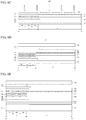
- FIGs. 6A to 6E are cross-sectional views showing a method of fabricating a display device according to a first embodiment of the present invention
- FIG. 7 is a view showing an adsorption and a desorption of a plurality of materials with respect to a surface energy of a display device according to a first embodiment of the present invention
- FIG. 8 is a behavior of a plurality of materials of a display device according to a first embodiment of the present invention.
- a plurality of thin film transistors such as a switching TFT Ts (of FIG. 2 ) and a driving TFT Td (of FIG. 2 ) and a storage capacitor Cs (of FIG. 2 ) may be disposed among a gate insulating layer 122, an interlayer insulating layer 124 and a passivation layer 126.
- the plurality of TFTs and a first electrode 128 may be formed through a photolithographic process.
- a first emission assisting layer 130 is formed on the entire surface of the substrate 120 having the first electrode 128, an emitting material layer 132 is formed in each of red, green and blue subpixels SPr, SPg and SPb on the first emission assisting layer 130, and a second emission assisting layer 134 is formed on a whole of the substrate 120 having the emitting material layer 132.
- the first emission assisting layer 130, the emitting material layer 132 and the second emission assisting layer 134 may be formed through a thermal evaporation process using a shadow mask such as a fine metal mask.
- An electron injecting layer of the second emission assisting layer 134 may be formed as a top surface of the substrate 120.
- the electron injecting layer which may comprise or consist of a metallic material, may have a relatively high surface energy.
- the electron injecting layer may have a surface energy equal to or greater than about 0.5 J/m 2 via a contact angle measurement.
- the metallic material for the electron injecting layer may have a relatively low melting point to be deposited at a relatively low temperature.
- the metallic material for the electron injecting layer may have a melting point equal to or lower than about 1000°C.
- the metallic material for the electron injecting layer may have a relatively great electric conductivity.
- the metallic material for the electron injecting layer may have an electric conductivity equal to or greater than about 4.0 ⁇ 10 6 ⁇ -1 m -1 .
- the metallic material for the electron injecting layer may have a relatively low work function.
- the metallic material for the electron injecting layer may have a work function of about 2.4 eV to about 2.8 eV.
- the electron injecting layer may have a thickness of about 10 ⁇ to about 40 ⁇ and may be formed with a deposition rate equal to or greater than about 0.05 ⁇ /sec.
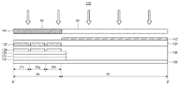
- a shadow mask 144 having a shielding area SA and an opening area OA is disposed over the second emission assisting layer 134, and an organic material is deposited on the second emission assisting layer 134 through the opening area OA.
- a deposition preventing layer 142 is formed in a transparent area TA on the second emission assisting layer 134, and the second emission assisting layer 134 of the display area DA is exposed.
- the shadow mask 144 may be aligned such that the shielding area SA and the opening area OA correspond to the display area DA and the transparent area TA, respectively.
- the deposition preventing layer 142 which may comprise or consist of an organic material, may have a relatively small surface energy and a relatively low glass transition temperature Tg.
- the deposition preventing layer 142 may have a surface energy equal to or smaller than about 0.2 J/m 2 and a glass transition temperature equal to or lower than about 40 °C.
- the organic material for the deposition preventing layer 142 may have a relatively great refractive index and a relatively small light absorption rate.
- the organic material for the deposition preventing layer 142 may have a refractive index equal to or greater than about 1.7 with respect to a light of a wavelength of about 550 nm and a light absorption rate equal to or smaller than about 0.02.
- the organic material for the deposition preventing layer 142 may be patterned using a shadow mask 144.
- the organic material for the deposition preventing layer 142 may be patterned through the shadow mask 144 to form a pattern corresponding to a pixel of a resolution of about 300 ppi.
- the organic material for the deposition preventing layer 142 may have a relatively great high temperature storage reliability.
- the organic material for the deposition preventing layer 142 may be determined such that deterioration does not occur even when the deposition preventing layer 142 of a thickness of about 300 ⁇ is left at a temperature of about 100 °C for about 500 hours.
- the deposition preventing layer 142 may have a thickness of about 20 ⁇ to about 300 ⁇ .
- the organic material for the deposition preventing layer 142 may be different from an organic insulating material such as photo acryl and polyimide used for the gate insulating layer 122, the interlayer insulating layer 124 and the passivation layer 126 and an inorganic insulating material such as silicon nitride (SiNx), silicon oxide (SiO 2 ) and silicon oxynitride (SiON).
- an organic insulating material such as photo acryl and polyimide used for the gate insulating layer 122, the interlayer insulating layer 124 and the passivation layer 126 and an inorganic insulating material such as silicon nitride (SiNx), silicon oxide (SiO 2 ) and silicon oxynitride (SiON).
- the organic insulating material for the gate insulating layer 122, the interlayer insulating layer 124 and the passivation layer 126 and the inorganic insulating material may be patterned through a photolithographic process
- the organic material for the deposition preventing layer 142 may not be patterned through a photolithographic process and may be patterned through a thermal deposition process using a shadow mask.
- the organic material for the deposition preventing layer 142 may include open-ring isomer diarylethene (DAE) expressed by a following chemical formula 1.
- DAE open-ring isomer diarylethene
- a metallic material is deposited on the second emission assisting layer 134 of the display area DA and the deposition preventing layer 142 of the transparent area TA.
- An atom 146 of the metallic material is not adsorbed onto and, if it happens to contact is desorbed immediately again due to a surface energy difference, from the deposition preventing layer 142 of the transparent area TA.
- the atom 146 of the metallic material is selectively adsorbed onto the second emission assisting layer 134 of the display area DA such that a second electrode 140 is selectively formed in the display area DA.
- the second electrode 140 which may comprise or consist of a metallic material, may have a relatively great surface energy.
- the second electrode 140 may have a surface energy equal to or greater than about 0.5 J/m 2 .
- a surface energy of the second electrode 140 may be greater than a surface energy the electron injecting layer of the second emission assisting layer 134.
- the metallic material for the second electrode 140 may have a relatively low melting point to be deposited at a relatively low temperature.
- the metallic material for the second electrode 140 may have a melting point equal to or lower than about 1000 °C.
- the metallic material for the second electrode 140 may have a relatively great electric conductivity.
- the metallic material for the second electrode 140 may have an electric conductivity equal to or greater than about 1.0 ⁇ 10 7 ⁇ -1 m -1 .
- the metallic material for the second electrode 140 may have a relatively small refractive index and a relatively small light absorption rate.
- the metallic material for the second electrode 140 may have a refractive index of about 1.0 with respect to a light of a wavelength of about 550 nm and a light absorption rate equal to or smaller than about 5.5.
- the metallic material for the second electrode 140 may have a thickness of about 100 ⁇ to about 200 ⁇ and may be formed with a deposition rate of about 0.1 ⁇ /sec to about 100 ⁇ /sec.
- the metallic material for the second emission assisting layer 134, the organic material for the deposition preventing layer 142 and the metallic material for the second electrode 140 have first, second and third surface energies SE1, SE2 and SE3, respectively.
- the first surface energy SE1 is greater than the second surface energy SE2 and is smaller than the third surface energy SE3. (SE2 ⁇ SE1 ⁇ SE3)
- the deposition preventing layer 142 which may be formed of an organic material, has the second surface energy SE2 of a relatively small value and a relatively low glass transition temperature, the deposition preventing layer 142 has an active surface atomic movement.
- the atom 146 of the metallic material for the second electrode 140 having the third surface energy SE3 is not adsorbed on and, if it happens to be adsorbed on is detached immediately again, from a surface of the deposition preventing layer 142 having the lowest surface energy SE2 of a relatively small value and a relatively low glass transition temperature in the transparent area TA and then moves to the display area DA.
- the atom 146 of the metallic material for the second electrode 140 having the third surface energy SE3 is selectively adsorbed on a surface of the electron injecting layer of the second emission assisting layer 134 having the first surface energy SE1 of a relatively great value in the display area DA.
- a nucleation of the atom 146 of the metallic material is performed and the atom 146 of the metallic material is gradually accumulated using a nucleus as a seed.
- the second electrode 140 is selectively formed in the display area DA.
- the second electrode 140 is selectively formed in the display area DA by adjusting the surface energies of the metallic material for the electron injecting layer of the second emission assisting layer 134, the organic material for the deposition preventing layer 142 and the metallic material for the second electrode 140 in the first embodiment, the second electrode 140 may also be selectively formed in the display area DA by adjusting deposition temperatures and deposition rates of the metallic material for the electron injecting layer of the second emission assisting layer 134, the organic material for the deposition preventing layer 142 and the metallic material for the second electrode 140 in another embodiment.
- an encapsulating layer 150 is formed on a whole of the substrate 120 having the second electrode 140 and the deposition preventing layer 142, and a touch layer 152 is formed on a whole of the substrate 120 having the encapsulating layer 150.
- a polarizing layer 154 is formed in the display area DA on the encapsulating layer 150.
- the polarizing layer 154 having a film type of a size corresponding to the display area DA may be attached to the encapsulating layer 150 of the display area DA.
- an adhesive layer 156 is formed in the display area DA on the polarizing layer 154, and a cover glass 160 is formed on a whole area of the substrate having the adhesive layer 156.
- the cover glass 160 may be attached to the polarizing layer 154 using the adhesive layer 156.
- a back plate 162 is formed on a whole of a rear surface of the substrate 120.
- the substrate 120 having the cover glass 160 may be attached to the back plate 162 using an adhesive layer.
- a system part 170 and an auxiliary equipment 172 are disposed in the display area DA and the transparent area TA, respectively, on the rear surface of the substrate 120.
- a cutting process of removing the light emitting diode and the encapsulating layer 150 of the transparent area TA is not performed.
- the metallic material for the second electrode 140 is not adsorbed on the deposition preventing layer 142 of the transparent area TA and is adsorbed on the second emission assisting layer 134 of the display area DA, the second electrode 140 of the light emitting diode is selectively formed in the display area DA such that a side surface of the light emitting diode and the encapsulating layer 150 is not exposed to the exterior.
- penetration of external oxygen or external moisture is minimized and deterioration is minimized.
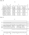
- FIG. 9 is a graph showing a transmittance of a display device according to a first embodiment of the present invention.
- FIG. 9 shows a transmittance of a display device where a cover glass 160 is omitted.
- the second electrode 140 is formed in the display area DA and is not formed in the transparent area TA due to the deposition preventing layer 142.
- a second electrode 140 being semitransparent is formed in a display area DA and a transparent area TA without a deposition preventing layer 142.
- the second electrode 140 includes magnesium silver (MgAg) and has a thickness of about 140 ⁇ .
- a transmittance of the transparent area TA of the display device 110 of the first embodiment is greater than a transmittance of the transparent area TA of the display device of the comparison example with respect to a light of a wavelength of about 400 nm to about 800 nm.
- the transparent area TA of the display device 110 of the first embodiment has intensities of about 107.6 %, about 107.2 % and about 108.0 % with respect to a light of wavelengths of about 430 nm, about 550 nm and about 620 nm, respectively.
- the transparent area TA of the display device of the comparison example has intensities of about 75.7%, about 75.8% and about 63.2% with respect to a light of wavelengths of about 430 nm, about 550 nm and about 620 nm, respectively.
- the transparent area TA of the display device 110 of the first embodiment has a greater transmittance by about 30% or more as compared with the transparent area TA of the display device of the comparison example, and a luminance of the display device 110 is improved.
- the transparent area TA of the display device 110 of the first embodiment has a uniform transmittance of a relatively high value, deterioration such as a color shift is minimized.
- the transparent area TA of the display device 110 of the first embodiment having the cover glass 160 may have intensities of about 97.6%, about 97.2% and about 98.0% with respect to a light of wavelengths of about 430 nm, about 550 nm and about 620 nm, respectively.
- the transparent area TA of the display device of the comparison example having the cover glass 160 has intensities of about 76.7%, about 65.8% and about 53.2% with respect to a light of wavelengths of about 430 nm, about 550 nm and about 620 nm, respectively.
- a cutting process of removing the light emitting diode and the encapsulating layer 150 of the transparent area TA is not performed. Instead, since the metallic material for the second electrode 140 is not adsorbed on the deposition preventing layer 142 of the transparent area TA and is adsorbed on the second emission assisting layer 134 of the display area DA, the second electrode 140 of the light emitting diode is selectively formed in the display area DA such that a side surface of the light emitting diode and the encapsulating layer 150 are not exposed to the exterior (e.g. the surrounding atmosphere).
- moisture penetration is increased. This can be observed in a storage reliability test which is carried out at a temperature of about 85°C and a humidity of about 85% for 200 hours.
- a storage reliability test which is carried out at a temperature of about 85°C and a humidity of about 85% for 200 hours.
- the second electrode 140 is selectively formed in the display area DA using the deposition preventing layer 142, increased moisture penetration is not observed in a storage reliability test that is carried out at a temperature of about 85°C and a humidity of about 85% for 408 hours.
- the transparent area TA has a uniform transmittance of a relatively high value, a luminance is improved and deterioration such as a color shift is minimized.
- a display quality of an image is improved by disposing color subpixels such as red, green and blue subpixels SPr, SPg and SPb in a portion of the transparent area TA.
- FIG. 10 is a magnified plan view showing a border region of a display area and a transparent area of a display device according to a second embodiment of the present invention
- FIG. 11 is a cross-sectional view taken along a line XI-XI of FIG. 10 .
- An organic light emitting diode (OLED) display device of an on-cell touch type and a top emission type is exemplarily illustrated as a display device.
- a display device 210 includes a display area DA used for displaying an image and sensing a touch, a transparent area TA inside the display area DA and a non-display area (not shown) surrounding the display area DA.
- the display device 210 includes a display panel, a system part 270 and an auxiliary equipment 272.
- the display panel may transmit an information to a user through an image displaying and may receive an information from the user through a touch sensing.
- the system part 270 may transmit and receive a signal and a power with the display panel and the auxiliary equipment 272.
- the auxiliary equipment 272 may receive an information such as a shape of a subject through the display panel.
- a back plate 262 supports and protects a substrate 220.
- the back plate 262 may include a plastic such as polyethylene terephthalate (PET) and may have a refractive index of about 1.6.
- PET polyethylene terephthalate
- the substrate 220 is disposed on a whole of the back plate 262, and a gate insulating layer 222, an interlayer insulating layer 224 and a passivation layer 226 are sequentially disposed in a plurality of first color subpixels of the display area DA and a plurality of second color subpixels of the transparent area TA on the substrate 220.
- the substrate 220 includes the display area DA and the transparent area TA.
- the display area DA includes the plurality of first color subpixels such as red, green and blue subpixels SPr, SPg and SPb
- the transparent area TA includes the plurality of second color subpixels such as red, green and blue subpixels SPr, SPg and SPb and a plurality of transparent subpixels SPt alternating with the plurality of second color subpixels.
- red, green and blue subpixels SPr, SPg and SPb of the plurality of second color subpixels and the plurality of transparent subpixels SPt of the transparent area TA exemplarily alternate with each other by 1:1 correspondence along a horizontal direction in the second embodiment
- the red, green and blue subpixels SPr, SPg and SPb of the plurality of second color subpixels and the plurality of transparent subpixels SPt of the transparent area TA may also alternate with each other by 1:plurality correspondence along a horizontal direction in another embodiment.
- the red, green and blue subpixels SPr, SPg and SPb of the plurality of second color subpixels and the plurality of transparent subpixels SPt of the transparent area TA may alternate with each other by 1:3 correspondence such that the transparent area TA has an aperture ratio of about 75%.
- the substrate 220 may include a glass or a plastic such as polyethylene terephthalate (PET) and may have a refractive index of about 1.6.
- PET polyethylene terephthalate
- a plurality of thin film transistors such as a switching TFT Ts (of FIG. 2 ) and a driving TFT Td (of FIG. 2 ) and a storage capacitor Cs (of FIG. 2 ) may be disposed among the gate insulating layer 222, the interlayer insulating layer 224 and the passivation layer 226 of each of the red, green and blue subpixels SPr, SPg and SPb.
- the gate insulating layer 222 may be disposed between a gate electrode and a semiconductor layer of the switching TFT Ts and the driving TFT Td
- the interlayer insulating layer 224 may be disposed between the gate electrode and a source electrode and between the gate electrode and a drain electrode of the switching TFT Ts and the driving TFT Td
- the passivation layer 226 may be disposed on the source electrode and the drain electrode of the switching TFT Ts and the driving TFT Td.
- a first electrode 228 is disposed in each of the red, green and blue subpixels SPr, SPg and SPb of the display area DA and the transparent area TA on the passivation layer 226, and a first emission assisting layer 230 is disposed on a whole of the substrate 220 having the first electrode 228.
- the first electrode 228 may include a first layer of a metallic material having a relatively high reflectance and a second layer of a transparent conductive material having a relatively high work function.
- the first electrode 228 may be an anode supplying a hole to an emitting material layer 232 and may be connected to the driving TFT Td.
- the first emission assisting layer 230 may include a hole injecting layer injecting a hole into the emitting material layer 232 and a hole transporting layer transporting a hole to the emitting material layer 232.
- the hole injecting layer and the hole transporting layer may be sequentially disposed on the first electrode 228.
- the emitting material layer 232 is disposed in each of the red, green and blue subpixels SPr, SPg and SPb on the first emission assisting layer 230, and a second emission assisting layer 234 is disposed on a whole of the substrate 220 having the emitting material layer 232.
- the emitting material layer 232 combines a hole supplied from the first electrode 228 and an electron supplied from a second electrode 240 to emit a light.
- the emitting material layers 232 of the red, green and blue subpixels SPr, SPg and SPb of the display area DA and the transparent area TA exemplarily include different materials to emit red, green and blue colored lights, respectively, in the second embodiment, the emitting material layers 232 of the red, green and blue subpixels SPr, SPg and SPb of the display area DA and the transparent area TA may have the same structure of the same material to emit a white colored light and a color filter layer may be disposed on the second electrode 240 in another embodiment.
- the second emission assisting layer 234 may include an electron transporting layer transporting an electron to the emitting material layer 232 and an electron injecting layer injecting an electron.
- the electron transporting layer and the electron injecting layer may be sequentially disposed on the emitting material layer 232.
- the electron injecting layer may have a thickness of about 10 ⁇ to about 40 ⁇ .
- Each of the first and second emission assisting layers 230 and 234 may have a refractive index of about 1.8.
- the first and second emission assisting layers 230 and 234 of the same material are exemplarily disposed on a whole of the substrate 220 in the second embodiment, the first and second emission assisting layers 230 and 234 may be selectively disposed in the red, green and blue subpixels SPr, SPg and SPb of the display area DA and the transparent area TA with different materials.
- the second electrode 240 is disposed in the red, green and blue subpixels SPr, SPg and SPb of the display area DA and the transparent area TA on the second emission assisting layer 234, and a deposition preventing layer 242 is disposed in the plurality of transparent subpixels SPt of the transparent area TA on the second emission assisting layer 234.
- the second electrode 240 is selectively disposed in a region where the deposition preventing layer 242 is not formed. As a result, and the second electrode 240 and the deposition preventing layer 242 may be disposed next to each other.
- the second electrode 240 may include a metallic material being semitransparent (e.g. half transparent) and having a relatively low work function.
- the second electrode 240 may be a cathode supplying an electron to the emitting material layer 232.
- the second electrode 240 may have a thickness of about 100 ⁇ to about 200 ⁇ and may include magnesium silver (MgAg).
- the first electrode 228, the first emission assisting layer 230, the emitting material layer 232, the second emission assisting layer 234 and the second electrode 240 constitute a light emitting diode.
- the deposition preventing layer 242 which may include an organic material, has a relatively low surface energy such that a metallic material is not adsorbed on and is detached from the deposition preventing layer 242 while the second electrode 240 is formed.
- the deposition preventing layer 242 may have a thickness of about 20 ⁇ to about 300 ⁇ .
- the deposition preventing layer 242 may be formed of the same material through the same process as the first embodiment.
- the second electrode 240 is not formed and the deposition preventing layer 242 is formed in the plurality of transparent subpixels SPt of the transparent area TA, a transmittance of the transparent area TA is improved.
- the plurality of transparent subpixels SPt of the transparent area TA may have a transmittance of about 94% and the transparent area TA may have an aperture ratio of about 75%.
- the transparent area TA without an anti-reflecting layer 258 may have a transmittance of about 71% and the transparent area TA with an anti-reflecting layer 258 may have a transmittance of about 75%.
- An encapsulating layer 250 is disposed on a whole of the substrate 220 having the second electrode 240 and the deposition preventing layer 242, and a touch layer 252 is disposed on a whole of the substrate 220 having the encapsulating layer 250.
- the encapsulating layer 250 prevents penetration of oxygen or moisture from the exterior (e.g. the surrounding atmosphere).
- the encapsulating layer 250 may include a plurality of organic material layers and a plurality of inorganic material layers and may have a refractive index of about 1.8.
- the touch layer 252 senses a touch.
- the touch layer 252 may include a plurality of touch electrodes and an insulating layer, and the insulating layer may have a refractive index of about 1.5.
- the touch layer 252 is exemplarily disposed on the encapsulating layer 250 in the second embodiment, the touch layer 252 may be disposed inside an array layer including the gate insulating layer 222, the interlayer insulating layer 224 and the passivation layer 226 or may be omitted in another embodiment.
- a polarizing layer 254 is disposed in the display area DA on the touch layer 252, and an adhesive layer 256 is disposed in the display area DA on the polarizing layer 254.
- the polarizing layer 254 minimizes re-emission of an external light by reflection on the array layer and the light emitting diode.
- the polarizing layer 254 may include a quarter wave plate and a linear polarizing layer sequentially on the touch layer 252.
- the anti-reflecting layer 258 is disposed in the transparent area TA on the touch layer 252.
- the anti-reflecting layer 258 improves a transmittance of the transparent area TA by adjusting an interference according to a reflection at an interface of the touch layer 252 and the anti-reflecting layer 258.
- the anti-reflecting layer 258 may be omitted in another embodiment.
- a cover glass 260 is disposed on a whole of the substrate 220 having the adhesive layer 256.
- the cover glass 260 protects the touch layer 252, the light emitting diode and the array layer.
- the back plate 262, the substrate 220, the plurality of TFTs, the light emitting diode and the cover glass 260 constitute the display panel.
- the system part 270 and the auxiliary equipment 272 are disposed in the display area DA and the transparent area TA, respectively, under the back plate 262.
- a cutting process of removing the light emitting diode and the encapsulating layer 250 of the transparent area TA is not performed. Instead, since the second electrode 240 of the light emitting diode is selectively formed in the plurality of first color subpixels of the display area DA and the plurality of second color subpixels of the transparent area TA using the deposition preventing layer 242, a side surface of the light emitting diode and the encapsulating layer 250 are not exposed to the exterior (e.g. the surrounding atmosphere). As a result, penetration of external oxygen or external moisture is minimized and deterioration is minimized.
- a display area of the display device 210 extends and a display quality of an image is improved.
- the light emitting diode including the second electrode 240 being semitransparent is disposed in the plurality of second color subpixels of the transparent area TA, a color reproducibility is improved due to a micro cavity effect and a lifetime increases.
- the deposition preventing layer 242 instead of the second electrode 240 is formed in the plurality of transparent subpixels SPt of the transparent area TA, a transmittance of the transparent area TA is improved.
- the second electrode of the light emitting diode is selectively disposed in the display area except for the transparent area using the deposition preventing layer, deterioration such as a particle is minimized, a fabrication cost is reduced, and a productivity is improved.
- the second electrode of the light emitting diode is selectively disposed in the display area and a portion of the transparent area using the deposition preventing layer, deterioration such as a particle is minimized, a fabrication cost is reduced, a productivity is improved, and an image is displayed even in the transparent area.
Landscapes
- Engineering & Computer Science (AREA)
- Chemical & Material Sciences (AREA)
- Physics & Mathematics (AREA)
- Inorganic Chemistry (AREA)
- Optics & Photonics (AREA)
- Microelectronics & Electronic Packaging (AREA)
- Manufacturing & Machinery (AREA)
- Life Sciences & Earth Sciences (AREA)
- Sustainable Development (AREA)
- Materials Engineering (AREA)
- Geometry (AREA)
- Devices For Indicating Variable Information By Combining Individual Elements (AREA)
- Spectroscopy & Molecular Physics (AREA)
- Electroluminescent Light Sources (AREA)
- Polarising Elements (AREA)
- Wood Science & Technology (AREA)
- Organic Chemistry (AREA)
- Physical Vapour Deposition (AREA)
- General Physics & Mathematics (AREA)
Abstract
Description
- The present application claims the priority of Republic of Korea Patent Application No.
10-2019-0160708 - The present invention relates to a display device, and more particularly, to a display device including a transparent area for an auxiliary equipment such as a camera or a fingerprint sensor and a method of fabricating the display device.
- A mobile terminal is a portable terminal capable of transmitting and receiving a voice, a character and an image data through a wireless communication. A flat panel display (FPD) such as an organic light emitting diode (OLED) display device may be used for the mobile terminal.
- Recently, a mobile terminal including an auxiliary equipment such as a camera for shooting and a fingerprint sensor for certification has been suggested.
- In the mobile terminal, the auxiliary equipment is disposed on a rear surface of a display panel, and the display panel includes a transparent area corresponding to the auxiliary equipment so that the auxiliary equipment can recognize a subject over a front surface of the display panel.
- To reduce a bezel of a non-display area and extend a display area, the transparent area for the auxiliary equipment is disposed inside the display area. After the display panel is completed, a substrate, an array layer, a light emitting diode, an encapsulating layer and a polarizing layer of the transparent area are removed through a cutting process such as a laser trimming. As a result, a transmittance of the transparent area may increase.
- However, fabrication costs are increased and a productivity is decreased due to the additional cutting process.
- In addition, since the light emitting diode and the encapsulating layer on the substrate are removed through the cutting process, a side surface of the light emitting diode and the encapsulating layer is exposed to the exterior (e.g. the surrounding atmosphere). As a result, oxygen or moisture from the exterior can get in through the side surface of the light emitting diode and the encapsulating layer and can result in a deterioration such as a particulate contaminant is generated in the display panel.
- To prevent the deterioration, the light emitting diode is separated by forming a groove in the array layer under the light emitting diode. However, this further increases fabrication costs and decreases productivity due to an additional groove forming step.
- Accordingly, the present invention is directed to a display device and a method of fabricating the display device that substantially obviate one or more of the problems due to limitations and disadvantages of the related art.
- An object of the present invention is to provide a display device including a transparent area and a method of fabricating said display device where a second electrode is selectively formed in a display area except the transparent area using a deposition preventing layer.
- Another object of the present invention is to provide a display device including a transparent area and a method of fabricating the display device where a second electrode is selectively formed in a display area and a portion of the transparent area.
- Additional features and advantages of the invention will be set forth in the description which follows.
- To achieve these and other advantages and in accordance with the purpose of the present invention, as embodied and broadly described herein, a display device includes: a substrate including a display area having a plurality of first color subpixels and a transparent area inside the display area; an array layer in the display area on the substrate; a first electrode in each of the plurality of first color subpixels on the array layer; a first emission assisting layer on the first electrode; an emitting material layer in each of the plurality of first color subpixels on the first emission assisting layer; a second emission assisting layer on the emitting material layer; a deposition preventing layer in the transparent area on the second emission assisting layer; a second electrode on the second emission assisting layer, the second electrode selectively disposed in a region where the deposition preventing layer is not disposed; an encapsulating layer on the deposition preventing layer and the second electrode; a polarizing layer in the display area on the encapsulating layer; and an auxiliary equipment in the transparent area under the substrate.
- In another aspect, a method of fabricating a display device includes: forming an array layer on a substrate including a display area having a plurality of first color subpixels and a transparent area inside the display area, the array layer disposed in the display area; forming a first electrode in each of the plurality of first color subpixels on the array layer; forming a first emission assisting layer on the first electrode; forming an emitting material layer in each of the plurality of first color subpixels on the first emission assisting layer; forming a second emission assisting layer on the emitting material layer; forming a deposition preventing layer in the transparent area on the second emission assisting layer; forming a second electrode on the second emission assisting layer, the second electrode selectively disposed in a region where the deposition preventing layer is not disposed; forming an encapsulating layer on the deposition preventing layer and the second electrode; forming a polarizing layer in the display area on the encapsulating layer; and forming an auxiliary equipment in the transparent area under the substrate.
- In the inventive device, the first emission assisting layer may include a hole injecting layer and a hole transporting layer which are sequentially disposed on the first electrode, and the second emission assisting layer may include an electron transporting layer and an electron injecting layer which are sequentially disposed on the emitting material layer.
- A surface energy of the electron injecting layer is preferably greater than a surface energy of the deposition preventing layer and smaller than a surface energy of the second electrode.
- More specifically, the electron injecting layer may have a surface energy which is equal to or greater than 0.5 J/m2. The deposition preventing layer may have a surface energy which is equal to or smaller than 0.2 J/m2. The second electrode may have a surface energy which is equal to or greater than 0.5 J/m2.
- Furthermore, the deposition preventing layer may have a glass transition temperature equal to or lower than 40°C and/or a refractive index equal to or greater than 1.7 with respect to a light of a wavelength of 550 nm and/or a light absorption rate equal to or smaller than 0.02 with respect to a light of a wavelength of 550 nm and/or a thickness of 20 Å to 300 Å.
- In a preferred embodiment, the deposition preventing layer includes an open-ring isomer diarylethene which is represented by the following chemical formula 1:

- In one embodiment of the present invention, the transparent area includes a plurality of second color subpixels and a plurality of transparent subpixels alternating with the plurality of second color subpixels, the array layer is further disposed in the plurality of second color subpixels on the substrate, the emitting material layer is further disposed in the plurality of second color subpixels on the first emission assisting layer, the deposition preventing layer is disposed in the plurality of transparent subpixels on the second emission assisting layer, and the second electrode is disposed in the display area and the plurality of second color subpixels on the second emission assisting layer.
- In the latter embodiment, it is preferred when the device further comprises an anti-reflecting layer in the transparent area on the encapsulating layer.
- Further, the device may comprise a touch layer between the encapsulating layer and the polarizing layer; a cover glass on the polarizing layer; a back plate between the substrate and the auxiliary equipment; and/or a system part in the display area under the back plate.
- Preferably, the deposition preventing layer is only disposed in the transparent area. More preferably, the deposition preventing layer is only disposed in the transparent area and the second electrode is only disposed in the display area.
- As far as the inventive method is concerned, the forming of a deposition preventing layer may comprise: disposing a shadow mask having a shielding area and an opening area over the second emission assisting layer; and depositing an organic material on the second emission assisting layer through the opening area of the shadow mask, wherein the shielding area and the opening area correspond to the display area and the transparent area, respectively.
- Besides that, forming the second electrode may comprise depositing a metallic material on the second emission assisting layer and, optionally, also the deposition preventing layer, wherein the metallic material, if it is adsorbed on the deposition preventing layer, is desorbed from the deposition preventing layer and is adsorbed on the second emission assisting layer.
- As indicated above, the device may have a transparent area which includes a plurality of second color subpixels and a plurality of transparent subpixels alternating with the plurality of second color subpixels. Then forming the array layer further comprises forming the array layer in the plurality of second color subpixels on the substrate, forming the emitting material layer further comprises forming the emitting material layer in the plurality of second color subpixels on the first emission assisting layer, forming the deposition preventing layer comprises forming the deposition preventing layer in the plurality of transparent subpixels on the second emission assisting layer, and forming the second electrode comprises forming the second electrode in the display area and the plurality of second color subpixels on the second emission assisting layer.
- The method may also further comprise forming an anti-reflecting layer in the transparent area on the encapsulating layer.
- Further preferable additional steps of the method include: forming a touch layer between the encapsulating layer and the polarizing layer; forming a cover glass on the polarizing layer; attaching a back plate to a rear surface of the substrate; and/or disposing a system part in the display area under the back plate.
- Apart from the above, it is also preferred when the deposition preventing layer is only disposed in the transparent area. It is even more preferred if the deposition preventing layer is only disposed in the transparent area and the second electrode is only disposed in the display area.
- It is to be understood that both, the foregoing general description and the following detailed description, are explanatory and are intended to provide further explanation of the invention as claimed.
- The accompanying drawings, which are included to provide further assistance in understanding the invention and are incorporated in and constitute a part of this specification, illustrate embodiments of the invention and together with the description serve to explain the principles of the invention. In the drawings:
-
FIG. 1 is a view showing a display device according to a first embodiment of the present invention; -
FIG. 2 is a view showing a subpixel of a display device according to a first embodiment of the present invention; -
FIG. 3 is a plan view showing a display device according to a first embodiment of the present invention; -
FIG. 4 is a magnified plan view showing a border region of a display area and a transparent area ofFIG. 3 ; -
FIG. 5 is a cross-sectional view taken along a line V-V ofFIG. 4 ; -
FIGs. 6A to 6E are cross-sectional views showing a method of fabricating a display device according to a first embodiment of the present invention; -
FIG. 7 is a view showing an adsorption and a desorption of a plurality of materials with respect to a surface energy of a display device according to a first embodiment of the present invention; -
FIG. 8 is a behavior of a plurality of materials of a display device according to a first embodiment of the present invention; -
FIG. 9 is a graph showing a transmittance of a display device according to a first embodiment of the present invention; -
FIG. 10 is a magnified plan view showing a border region of a display area and a transparent area of a display device according to a second embodiment of the present invention; and -
FIG. 11 is a cross-sectional view taken along a line XI-XI ofFIG. 10 . - Advantages and features of the present invention, and implementation methods thereof will be clarified through the following exemplary embodiments that are described with a reference to the accompanying drawings. The present invention may, however, be embodied in different forms and should not be construed as being limited to the exemplary embodiments set forth herein. Rather, these exemplary embodiments are provided so that the disclosure of this invention is detailed enough and complete to assist those skilled in the art to fully understand the subject-matter
- A shape, a size, a ratio, an angle, and a number disclosed in the drawings for describing embodiments of the present invention are merely examples. Thus, the present invention is not limited to the illustrated details. The same reference numerals refer to the same elements throughout. In the following description, when the detailed description of the relevant known function or configuration is determined to unnecessarily obscure an important point of the present invention, the detailed description of such known function or configuration may be omitted. In a case where terms "comprise", "have", and "include" described in the present specification are used, another part may be added unless a more limiting term, such as "only", is used. Terms that are used in a singular form may include plural forms unless otherwise indicated.
- In construing an element, the element is construed as including an error or tolerance range even when there is no explicit description of such an error or tolerance range.
- In describing a position relationship, when a position relation between two parts is described as, for example, "on", "over", "under", or "next", one or more other parts may be disposed between the two parts unless a more limiting term, such as "just" or "direct(ly)", is used.
- It will be understood that, although the terms "first", "second", etc. may be used herein to describe various elements, these elements should not be limited by these terms. These terms are only used to distinguish one element from another. For example, a first element could also be termed a second element, and, similarly, a second element could also be termed a first element, without departing from the scope of the present invention.
- Features of various embodiments of the present invention may be partially or overall coupled to or combined with each other, and may be variously inter-operated with each other and driven technically as those skilled in the art can sufficiently understand. Embodiments of the present invention may be carried out independently from each other, or may be carried out together in co-dependent relationship.
- Hereinafter, a display device and a method of fabricating the display device according to embodiments of the present invention will be described in detail with reference to the accompanying drawings.
-
FIG. 1 is a view showing a display device according to a first embodiment of the present invention, andFIG. 2 is a view showing a subpixel of a display device according to a first embodiment of the present invention. An organic light emitting diode(OLED) display device is exemplarily illustrated as a display device inFIGs. 1 and 2 . - In
FIG. 1 , adisplay device 110 includes atiming controlling part 180, adata driving part 182, agate driving part 184 and adisplay panel 186. - The
timing controlling part 180 generates a gate control signal, a data control signal and an image data using an image signal and a plurality of timing signals transmitted from an external system such as a graphic card or a television system. Thetiming controlling part 180 supplies the data control signal and the image data to thedata driving part 182 and supplies the gate control signal to thegate driving part 184. - The
data driving part 182 generates a data signal (a data voltage) using the data control signal and the image data transmitted from thetiming controlling part 180 and supplies the data voltage to a data line DL of thedisplay panel 186. - The
gate driving part 184 generates a gate signal (a gate voltage) using the gate control signal transmitted from thetiming controlling part 180 and supplies the gate voltage to a gate line GL of thedisplay panel 186. - The
display panel 186 displays an image using the gate signal and the data signal. Thedisplay panel 186 includes the gate line GL, the data line DL and a plurality of subpixels SP (ofFIG. 2 ) connected to the gate line GL and the data line DL. - For example, each of the plurality of subpixels SP may be defined by the gate line GL and the data line DL crossing each other, and the plurality of subpixels SP may include red, green and blue subpixels SPr, SPg and SPb corresponding to red, green and blue colors, respectively.
- Each of the plurality of subpixels SP includes a plurality of thin film transistors (TFTs). For example, each of the plurality of subpixels SP may include a switching TFT, a driving TFT, a storage capacitor and a light emitting diode.
- In
FIG. 2 , each of the plurality of subpixels SP of theOLED display device 110 according to a first embodiment of the present invention includes a switching TFT Ts, a driving TFT Td, a storage capacitor Cs and a light emitting diode De. - The switching TFT Ts supplies the data signal of the data line DL to the driving TFT Td according to the gate signal of the gate line GL, and the driving TFT Td supplies a high level voltage ELVDD to the light emitting diode De according to the data signal applied to a gate electrode through the switching TFT Ts.
- The light emitting diode De displays various gray levels using various currents according to voltage differences between a voltage corresponding to the data signal and a low level voltage ELVSS.
-
FIG. 3 is a plan view showing a display device according to a first embodiment of the present invention,FIG. 4 is a magnified plan view showing a border region of a display area and a transparent area ofFIG. 3 , andFIG. 5 is a cross-sectional view taken along a line V-V ofFIG. 4 . An organic light emitting diode (OLED) display device of an on-cell touch type and a top emission type is exemplarily illustrated as a display device. - In
FIGs. 3, 4 and5 , adisplay device 110 according to a first embodiment of the present invention includes a display area DA used for displaying an image and sensing a touch, a transparent area TA inside the display area DA and a non-display area NDA surrounding the display area DA. - The
display device 110 includes adisplay panel 186, asystem part 170 and anauxiliary equipment 172. Thedisplay panel 186 may transmit an information to a user through an image displaying and may receive an information from the user through a touch sensing. Thesystem part 170 may transmit and receive a signal and a power with the display panel and theauxiliary equipment 172. Theauxiliary equipment 172 may receive an information such as a shape of a subject through thedisplay panel 186. - A
back plate 162 supports and protects asubstrate 120. Theback plate 162 may include a plastic such as polyethylene terephthalate (PET) and may have a refractive index of about 1.6. - The
substrate 120 is disposed on the entire surface of theback plate 162, and agate insulating layer 122, aninterlayer insulating layer 124 and apassivation layer 126 are sequentially disposed in the display area DA on thesubstrate 120. - The
substrate 120 includes the display area DA and the transparent area TA. The display area DA includes a plurality of first color subpixels such as red, green and blue subpixels SPr, SPg and SPb, and the transparent area TA is disposed inside the display area DA. - The
substrate 120 may include a glass or a plastic such as polyethylene terephthalate (PET) and may have a refractive index of about 1.6. - A plurality of thin film transistors (TFTs) such as a switching TFT Ts (of
FIG. 2 ) and a driving TFT Td (ofFIG. 2 ) and a storage capacitor Cs (ofFIG. 2 ) may be disposed among thegate insulating layer 122, theinterlayer insulating layer 124 and thepassivation layer 126 of each of the red, green and blue subpixels SPr, SPg and SPb. - For example, the
gate insulating layer 122 may be disposed between a gate electrode and a semiconductor layer of the switching TFT Ts and the driving TFT Td, theinterlayer insulating layer 124 may be disposed between the gate electrode and a source electrode and between the gate electrode and a drain electrode of the switching TFT Ts and the driving TFT Td, and thepassivation layer 126 may be disposed on the source electrode and the drain electrode of the switching TFT Ts and the driving TFT Td. - A
first electrode 128 is disposed in each of the red, green and blue subpixels SPr, SPg and SPb on thepassivation layer 126, and a firstemission assisting layer 130 is disposed on the entire surface of thesubstrate 120 having thefirst electrode 128. - The
first electrode 128 may include a first layer of a metallic material having a relatively high reflectance and a second layer of a transparent conductive material having a relatively high work function. - For example, the
first electrode 128 may be an anode supplying a hole to an emittingmaterial layer 132 and may be connected to the driving TFT Td. - The first
emission assisting layer 130 may include a hole injecting layer injecting a hole into the emittingmaterial layer 132 and a hole transporting layer transporting a hole to the emittingmaterial layer 132. The hole injecting layer and the hole transporting layer may be sequentially disposed on thefirst electrode 128. - The emitting
material layer 132 is disposed in each of the red, green and blue subpixels SPr, SPg and SPb on the firstemission assisting layer 130, and a secondemission assisting layer 134 is disposed on the entire surface of thesubstrate 120 having the emittingmaterial layer 132. - The emitting
material layer 132 combines a hole supplied from thefirst electrode 128 and an electron supplied from asecond electrode 140 to emit a light. - Although the emitting material layers 132 of the red, green and blue subpixels SPr, SPg and SPb exemplarily include different materials to emit red, green and blue colored lights, respectively, in the first embodiment, the emitting material layers 132 of the red, green and blue subpixels SPr, SPg and SPb may have the same structure of the same material to emit a white colored light and a color filter layer may be disposed on the
second electrode 140 in another embodiment. - The second
emission assisting layer 134 may include an electron transporting layer transporting an electron to the emittingmaterial layer 132 and an electron injecting layer injecting an electron. The electron transporting layer and the electron injecting layer may be sequentially disposed on the emittingmaterial layer 132. - For example, the electron injecting layer may have a thickness of about 10Å to about 40Å.
- Each of the first and second
emission assisting layer - Although the first and second
emission assisting layers substrate 120 in the first embodiment, the first and secondemission assisting layers - The
second electrode 140 and adeposition preventing layer 142 are disposed in the display area DA and the transparent area TA, respectively, on the secondemission assisting layer 134. - The
second electrode 140 is selectively disposed in a region where thedeposition preventing layer 142 is not formed. As a result, thesecond electrode 140 and thedeposition preventing layer 142 may be disposed next to each other. - The
second electrode 140 may include a metallic material being semitransparent (e.g. half transparent) and a relatively low work function. - For example, the
second electrode 140 may be a cathode supplying an electron to the emittingmaterial layer 132. Thesecond electrode 140 may have a thickness of about 100Å to about 200Å and may include magnesium silver (MgAg). - The
first electrode 128, the firstemission assisting layer 130, the emittingmaterial layer 132, the secondemission assisting layer 134 and thesecond electrode 140 constitute a light emitting diode. - The
deposition preventing layer 142, which may include an organic material, may have a relatively low surface energy such that a metallic material is not adsorbed on and is detached from thedeposition preventing layer 142 while thesecond electrode 140 is formed. - For example, the
deposition preventing layer 142 may have a thickness of about 20Å to about 300Å. - The
deposition preventing layer 142 will be illustrated later. - An
encapsulating layer 150 is disposed on the entire surface of thesubstrate 120 having thesecond electrode 140 and thedeposition preventing layer 142, and atouch layer 152 is disposed on the entire surface of thesubstrate 120 having theencapsulating layer 150. - The
encapsulating layer 150 prevents penetration of oxygen or moisture from the exterior. Theencapsulating layer 150 may include a plurality of organic material layers and a plurality of inorganic material layers and may have a refractive index of about 1.8. - The
touch layer 152 senses a touch. Thetouch layer 152 may include a plurality of touch electrodes and an insulating layer, and the insulating layer may have a refractive index of about 1.5. - Although the
touch layer 152 is exemplarily disposed on theencapsulating layer 150 in the first embodiment, thetouch layer 152 may be disposed inside an array layer including thegate insulating layer 122, theinterlayer insulating layer 124 and thepassivation layer 126 or may be omitted in another embodiment. - A
polarizing layer 154 is disposed in the display area DA on thetouch layer 152, and anadhesive layer 156 is disposed in the display area DA on thepolarizing layer 154. - The
polarizing layer 154 minimizes re-emission of an external light by reflection on the array layer and the light emitting diode. Thepolarizing layer 154 may include a quarter wave plate and a linear polarizing layer sequentially on thetouch layer 152. - A
cover glass 160 is disposed on the entire surface of thesubstrate 120 having theadhesive layer 156. Thecover glass 160 protects thetouch layer 152, the light emitting diode and the plurality of TFTs. - The
back plate 162, thesubstrate 120, the plurality of TFTs, the light emitting diode and thecover glass 160 constitute the display panel. - The
system part 170 and theauxiliary equipment 172 are disposed in the display area DA and the transparent area TA, respectively, under theback plate 162. - In the
display device 110 according to a first embodiment of the present invention, a cutting process of removing the light emitting diode and theencapsulating layer 150 of the transparent area TA is not performed. Instead, since thesecond electrode 140 of the light emitting diode is selectively formed in the display area DA using thedeposition preventing layer 142, a side surface of the light emitting diode and theencapsulating layer 150 is not exposed to the exterior. As a result, penetration of external oxygen or external moisture is minimized and deterioration such as a particle is minimized. - In addition, since a cutting process such as a laser trimming and a process of forming a groove are omitted, a fabrication process is simplified, a fabrication cost is reduced, and a productivity is improved.
- A method of fabricating the
display device 110 is illustrated hereinafter. -
FIGs. 6A to 6E are cross-sectional views showing a method of fabricating a display device according to a first embodiment of the present invention,FIG. 7 is a view showing an adsorption and a desorption of a plurality of materials with respect to a surface energy of a display device according to a first embodiment of the present invention, andFIG. 8 is a behavior of a plurality of materials of a display device according to a first embodiment of the present invention. - In
FIG. 6A , a plurality of thin film transistors (TFTs) such as a switching TFT Ts (ofFIG. 2 ) and a driving TFT Td (ofFIG. 2 ) and a storage capacitor Cs (ofFIG. 2 ) may be disposed among agate insulating layer 122, aninterlayer insulating layer 124 and apassivation layer 126. - The plurality of TFTs and a
first electrode 128 may be formed through a photolithographic process. - Next, a first
emission assisting layer 130 is formed on the entire surface of thesubstrate 120 having thefirst electrode 128, an emittingmaterial layer 132 is formed in each of red, green and blue subpixels SPr, SPg and SPb on the firstemission assisting layer 130, and a secondemission assisting layer 134 is formed on a whole of thesubstrate 120 having the emittingmaterial layer 132. - The first
emission assisting layer 130, the emittingmaterial layer 132 and the secondemission assisting layer 134 may be formed through a thermal evaporation process using a shadow mask such as a fine metal mask. - An electron injecting layer of the second
emission assisting layer 134 may be formed as a top surface of thesubstrate 120. - The electron injecting layer, which may comprise or consist of a metallic material, may have a relatively high surface energy. For example, the electron injecting layer may have a surface energy equal to or greater than about 0.5 J/m2 via a contact angle measurement.
- The metallic material for the electron injecting layer may have a relatively low melting point to be deposited at a relatively low temperature. For example, the metallic material for the electron injecting layer may have a melting point equal to or lower than about 1000°C.
- The metallic material for the electron injecting layer may have a relatively great electric conductivity. For example, the metallic material for the electron injecting layer may have an electric conductivity equal to or greater than about 4.0∗106Ω-1m-1.
- The metallic material for the electron injecting layer may have a relatively low work function. For example, the metallic material for the electron injecting layer may have a work function of about 2.4 eV to about 2.8 eV.
- The electron injecting layer may have a thickness of about 10 Å to about 40 Å and may be formed with a deposition rate equal to or greater than about 0.05 Å/sec.
- In
FIG. 6B , ashadow mask 144 having a shielding area SA and an opening area OA is disposed over the secondemission assisting layer 134, and an organic material is deposited on the secondemission assisting layer 134 through the opening area OA. - As a result, a
deposition preventing layer 142 is formed in a transparent area TA on the secondemission assisting layer 134, and the secondemission assisting layer 134 of the display area DA is exposed. - The
shadow mask 144 may be aligned such that the shielding area SA and the opening area OA correspond to the display area DA and the transparent area TA, respectively. - The
deposition preventing layer 142, which may comprise or consist of an organic material, may have a relatively small surface energy and a relatively low glass transition temperature Tg. For example, thedeposition preventing layer 142 may have a surface energy equal to or smaller than about 0.2 J/m2 and a glass transition temperature equal to or lower than about 40 °C. - The organic material for the
deposition preventing layer 142 may have a relatively great refractive index and a relatively small light absorption rate. For example, the organic material for thedeposition preventing layer 142 may have a refractive index equal to or greater than about 1.7 with respect to a light of a wavelength of about 550 nm and a light absorption rate equal to or smaller than about 0.02. - The organic material for the
deposition preventing layer 142 may be patterned using ashadow mask 144. For example, the organic material for thedeposition preventing layer 142 may be patterned through theshadow mask 144 to form a pattern corresponding to a pixel of a resolution of about 300 ppi. - The organic material for the
deposition preventing layer 142 may have a relatively great high temperature storage reliability. For example, the organic material for thedeposition preventing layer 142 may be determined such that deterioration does not occur even when thedeposition preventing layer 142 of a thickness of about 300 Å is left at a temperature of about 100 °C for about 500 hours. - The
deposition preventing layer 142 may have a thickness of about 20 Å to about 300 Å. - The organic material for the
deposition preventing layer 142 may be different from an organic insulating material such as photo acryl and polyimide used for thegate insulating layer 122, theinterlayer insulating layer 124 and thepassivation layer 126 and an inorganic insulating material such as silicon nitride (SiNx), silicon oxide (SiO2) and silicon oxynitride (SiON). - While the organic insulating material for the
gate insulating layer 122, theinterlayer insulating layer 124 and thepassivation layer 126 and the inorganic insulating material may be patterned through a photolithographic process, the organic material for thedeposition preventing layer 142 may not be patterned through a photolithographic process and may be patterned through a thermal deposition process using a shadow mask. - For example, the organic material for the
deposition preventing layer 142 may include open-ring isomer diarylethene (DAE) expressed by a following chemical formula 1.
- In
FIG. 6C , a metallic material is deposited on the secondemission assisting layer 134 of the display area DA and thedeposition preventing layer 142 of the transparent area TA. - An
atom 146 of the metallic material is not adsorbed onto and, if it happens to contact is desorbed immediately again due to a surface energy difference, from thedeposition preventing layer 142 of the transparent area TA. Theatom 146 of the metallic material is selectively adsorbed onto the secondemission assisting layer 134 of the display area DA such that asecond electrode 140 is selectively formed in the display area DA. - The
second electrode 140, which may comprise or consist of a metallic material, may have a relatively great surface energy. For example, thesecond electrode 140 may have a surface energy equal to or greater than about 0.5 J/m2. - Specifically, a surface energy of the
second electrode 140 may be greater than a surface energy the electron injecting layer of the secondemission assisting layer 134. - The metallic material for the
second electrode 140 may have a relatively low melting point to be deposited at a relatively low temperature. For example, the metallic material for thesecond electrode 140 may have a melting point equal to or lower than about 1000 °C. - The metallic material for the
second electrode 140 may have a relatively great electric conductivity. For example, the metallic material for thesecond electrode 140 may have an electric conductivity equal to or greater than about 1.0∗107Ω-1m-1. - The metallic material for the
second electrode 140 may have a relatively small refractive index and a relatively small light absorption rate. For example, the metallic material for thesecond electrode 140 may have a refractive index of about 1.0 with respect to a light of a wavelength of about 550 nm and a light absorption rate equal to or smaller than about 5.5. - The metallic material for the
second electrode 140 may have a thickness of about 100 Å to about 200 Å and may be formed with a deposition rate of about 0.1 Å/sec to about 100 Å/sec. - In
FIGs. 7 and 8 , the metallic material for the secondemission assisting layer 134, the organic material for thedeposition preventing layer 142 and the metallic material for thesecond electrode 140 have first, second and third surface energies SE1, SE2 and SE3, respectively. The first surface energy SE1 is greater than the second surface energy SE2 and is smaller than the third surface energy SE3. (SE2 < SE1 < SE3) - Since the
deposition preventing layer 142, which may be formed of an organic material, has the second surface energy SE2 of a relatively small value and a relatively low glass transition temperature, thedeposition preventing layer 142 has an active surface atomic movement. - As a result, the
atom 146 of the metallic material for thesecond electrode 140 having the third surface energy SE3 is not adsorbed on and, if it happens to be adsorbed on is detached immediately again, from a surface of thedeposition preventing layer 142 having the lowest surface energy SE2 of a relatively small value and a relatively low glass transition temperature in the transparent area TA and then moves to the display area DA. - The
atom 146 of the metallic material for thesecond electrode 140 having the third surface energy SE3 is selectively adsorbed on a surface of the electron injecting layer of the secondemission assisting layer 134 having the first surface energy SE1 of a relatively great value in the display area DA. In the display area DA, a nucleation of theatom 146 of the metallic material is performed and theatom 146 of the metallic material is gradually accumulated using a nucleus as a seed. As a result, thesecond electrode 140 is selectively formed in the display area DA. - Although the
second electrode 140 is selectively formed in the display area DA by adjusting the surface energies of the metallic material for the electron injecting layer of the secondemission assisting layer 134, the organic material for thedeposition preventing layer 142 and the metallic material for thesecond electrode 140 in the first embodiment, thesecond electrode 140 may also be selectively formed in the display area DA by adjusting deposition temperatures and deposition rates of the metallic material for the electron injecting layer of the secondemission assisting layer 134, the organic material for thedeposition preventing layer 142 and the metallic material for thesecond electrode 140 in another embodiment. - In
FIG. 6D , anencapsulating layer 150 is formed on a whole of thesubstrate 120 having thesecond electrode 140 and thedeposition preventing layer 142, and atouch layer 152 is formed on a whole of thesubstrate 120 having theencapsulating layer 150. - Next, a
polarizing layer 154 is formed in the display area DA on theencapsulating layer 150. For example, thepolarizing layer 154 having a film type of a size corresponding to the display area DA may be attached to theencapsulating layer 150 of the display area DA. - Next, an
adhesive layer 156 is formed in the display area DA on thepolarizing layer 154, and acover glass 160 is formed on a whole area of the substrate having theadhesive layer 156. - For example, the
cover glass 160 may be attached to thepolarizing layer 154 using theadhesive layer 156. - Next, a
back plate 162 is formed on a whole of a rear surface of thesubstrate 120. - For example, the
substrate 120 having thecover glass 160 may be attached to theback plate 162 using an adhesive layer. - In
FIG. 6E , asystem part 170 and anauxiliary equipment 172 are disposed in the display area DA and the transparent area TA, respectively, on the rear surface of thesubstrate 120. - In the method of fabricating the
display device 110 according to a first embodiment of the present invention, a cutting process of removing the light emitting diode and theencapsulating layer 150 of the transparent area TA is not performed. Instead, since the metallic material for thesecond electrode 140 is not adsorbed on thedeposition preventing layer 142 of the transparent area TA and is adsorbed on the secondemission assisting layer 134 of the display area DA, thesecond electrode 140 of the light emitting diode is selectively formed in the display area DA such that a side surface of the light emitting diode and theencapsulating layer 150 is not exposed to the exterior. As a result, penetration of external oxygen or external moisture is minimized and deterioration is minimized. - In addition, since a cutting process such as a laser trimming and a process of forming a groove are omitted, a fabrication process is simplified, a fabrication cost is reduced, and a productivity is improved.
-
FIG. 9 is a graph showing a transmittance of a display device according to a first embodiment of the present invention.FIG. 9 shows a transmittance of a display device where acover glass 160 is omitted. - In the
display device 110 according to a first embodiment of the present invention ofFIG. 9 , thesecond electrode 140 is formed in the display area DA and is not formed in the transparent area TA due to thedeposition preventing layer 142. - In a display device according to a comparison example, a
second electrode 140 being semitransparent (e.g. half transparent) is formed in a display area DA and a transparent area TA without adeposition preventing layer 142. - The
second electrode 140 includes magnesium silver (MgAg) and has a thickness of about 140 Å. - A transmittance of the transparent area TA of the
display device 110 of the first embodiment is greater than a transmittance of the transparent area TA of the display device of the comparison example with respect to a light of a wavelength of about 400 nm to about 800 nm. - The transparent area TA of the
display device 110 of the first embodiment has intensities of about 107.6 %, about 107.2 % and about 108.0 % with respect to a light of wavelengths of about 430 nm, about 550 nm and about 620 nm, respectively. The transparent area TA of the display device of the comparison example has intensities of about 75.7%, about 75.8% and about 63.2% with respect to a light of wavelengths of about 430 nm, about 550 nm and about 620 nm, respectively. - As a result, the transparent area TA of the
display device 110 of the first embodiment has a greater transmittance by about 30% or more as compared with the transparent area TA of the display device of the comparison example, and a luminance of thedisplay device 110 is improved. - In addition, since the transparent area TA of the
display device 110 of the first embodiment has a uniform transmittance of a relatively high value, deterioration such as a color shift is minimized. - The transparent area TA of the
display device 110 of the first embodiment having thecover glass 160 may have intensities of about 97.6%, about 97.2% and about 98.0% with respect to a light of wavelengths of about 430 nm, about 550 nm and about 620 nm, respectively. The transparent area TA of the display device of the comparison example having thecover glass 160 has intensities of about 76.7%, about 65.8% and about 53.2% with respect to a light of wavelengths of about 430 nm, about 550 nm and about 620 nm, respectively. - In the
display device 110 according to a first embodiment of the present invention, a cutting process of removing the light emitting diode and theencapsulating layer 150 of the transparent area TA is not performed. Instead, since the metallic material for thesecond electrode 140 is not adsorbed on thedeposition preventing layer 142 of the transparent area TA and is adsorbed on the secondemission assisting layer 134 of the display area DA, thesecond electrode 140 of the light emitting diode is selectively formed in the display area DA such that a side surface of the light emitting diode and theencapsulating layer 150 are not exposed to the exterior (e.g. the surrounding atmosphere). - As a result, penetration of external oxygen or external moisture is minimized and deterioration is minimized.
- For example, in the display device of the comparison example where the light emitting diode and the
encapsulating layer 150 of the transparent area TA are removed through a cutting process such as a laser trimming, moisture penetration is increased. This can be observed in a storage reliability test which is carried out at a temperature of about 85°C and a humidity of about 85% for 200 hours. In thedisplay device 110 of the first embodiment where thesecond electrode 140 is selectively formed in the display area DA using thedeposition preventing layer 142, increased moisture penetration is not observed in a storage reliability test that is carried out at a temperature of about 85°C and a humidity of about 85% for 408 hours. - In addition, since a cutting process such as a laser trimming and a process of forming a groove are omitted, a fabrication process is simplified, a fabrication cost is reduced, and a productivity is improved.
- Further, since the transparent area TA has a uniform transmittance of a relatively high value, a luminance is improved and deterioration such as a color shift is minimized.
- In another embodiment, a display quality of an image is improved by disposing color subpixels such as red, green and blue subpixels SPr, SPg and SPb in a portion of the transparent area TA.
-
FIG. 10 is a magnified plan view showing a border region of a display area and a transparent area of a display device according to a second embodiment of the present invention, andFIG. 11 is a cross-sectional view taken along a line XI-XI ofFIG. 10 . An organic light emitting diode (OLED) display device of an on-cell touch type and a top emission type is exemplarily illustrated as a display device. - In
FIGs. 10 and 11 , adisplay device 210 according to a second embodiment of the present invention includes a display area DA used for displaying an image and sensing a touch, a transparent area TA inside the display area DA and a non-display area (not shown) surrounding the display area DA. - The
display device 210 includes a display panel, asystem part 270 and anauxiliary equipment 272. The display panel may transmit an information to a user through an image displaying and may receive an information from the user through a touch sensing. Thesystem part 270 may transmit and receive a signal and a power with the display panel and theauxiliary equipment 272. Theauxiliary equipment 272 may receive an information such as a shape of a subject through the display panel. - A
back plate 262 supports and protects asubstrate 220. Theback plate 262 may include a plastic such as polyethylene terephthalate (PET) and may have a refractive index of about 1.6. - The
substrate 220 is disposed on a whole of theback plate 262, and agate insulating layer 222, aninterlayer insulating layer 224 and apassivation layer 226 are sequentially disposed in a plurality of first color subpixels of the display area DA and a plurality of second color subpixels of the transparent area TA on thesubstrate 220. - The
substrate 220 includes the display area DA and the transparent area TA. The display area DA includes the plurality of first color subpixels such as red, green and blue subpixels SPr, SPg and SPb, and the transparent area TA includes the plurality of second color subpixels such as red, green and blue subpixels SPr, SPg and SPb and a plurality of transparent subpixels SPt alternating with the plurality of second color subpixels. - Although the red, green and blue subpixels SPr, SPg and SPb of the plurality of second color subpixels and the plurality of transparent subpixels SPt of the transparent area TA exemplarily alternate with each other by 1:1 correspondence along a horizontal direction in the second embodiment, the red, green and blue subpixels SPr, SPg and SPb of the plurality of second color subpixels and the plurality of transparent subpixels SPt of the transparent area TA may also alternate with each other by 1:plurality correspondence along a horizontal direction in another embodiment.
- For example, the red, green and blue subpixels SPr, SPg and SPb of the plurality of second color subpixels and the plurality of transparent subpixels SPt of the transparent area TA may alternate with each other by 1:3 correspondence such that the transparent area TA has an aperture ratio of about 75%.
- The
substrate 220 may include a glass or a plastic such as polyethylene terephthalate (PET) and may have a refractive index of about 1.6. - A plurality of thin film transistors (TFTs) such as a switching TFT Ts (of
FIG. 2 ) and a driving TFT Td (ofFIG. 2 ) and a storage capacitor Cs (ofFIG. 2 ) may be disposed among thegate insulating layer 222, theinterlayer insulating layer 224 and thepassivation layer 226 of each of the red, green and blue subpixels SPr, SPg and SPb. - For example, the
gate insulating layer 222 may be disposed between a gate electrode and a semiconductor layer of the switching TFT Ts and the driving TFT Td, theinterlayer insulating layer 224 may be disposed between the gate electrode and a source electrode and between the gate electrode and a drain electrode of the switching TFT Ts and the driving TFT Td, and thepassivation layer 226 may be disposed on the source electrode and the drain electrode of the switching TFT Ts and the driving TFT Td. - A
first electrode 228 is disposed in each of the red, green and blue subpixels SPr, SPg and SPb of the display area DA and the transparent area TA on thepassivation layer 226, and a firstemission assisting layer 230 is disposed on a whole of thesubstrate 220 having thefirst electrode 228. - The
first electrode 228 may include a first layer of a metallic material having a relatively high reflectance and a second layer of a transparent conductive material having a relatively high work function. - For example, the
first electrode 228 may be an anode supplying a hole to an emittingmaterial layer 232 and may be connected to the driving TFT Td. - The first
emission assisting layer 230 may include a hole injecting layer injecting a hole into the emittingmaterial layer 232 and a hole transporting layer transporting a hole to the emittingmaterial layer 232. The hole injecting layer and the hole transporting layer may be sequentially disposed on thefirst electrode 228. - The emitting
material layer 232 is disposed in each of the red, green and blue subpixels SPr, SPg and SPb on the firstemission assisting layer 230, and a secondemission assisting layer 234 is disposed on a whole of thesubstrate 220 having the emittingmaterial layer 232. - The emitting
material layer 232 combines a hole supplied from thefirst electrode 228 and an electron supplied from asecond electrode 240 to emit a light. - Although the emitting material layers 232 of the red, green and blue subpixels SPr, SPg and SPb of the display area DA and the transparent area TA exemplarily include different materials to emit red, green and blue colored lights, respectively, in the second embodiment, the emitting material layers 232 of the red, green and blue subpixels SPr, SPg and SPb of the display area DA and the transparent area TA may have the same structure of the same material to emit a white colored light and a color filter layer may be disposed on the
second electrode 240 in another embodiment. - The second
emission assisting layer 234 may include an electron transporting layer transporting an electron to the emittingmaterial layer 232 and an electron injecting layer injecting an electron. The electron transporting layer and the electron injecting layer may be sequentially disposed on the emittingmaterial layer 232. - For example, the electron injecting layer may have a thickness of about 10 Å to about 40 Å.
- Each of the first and second
emission assisting layers - Although the first and second
emission assisting layers substrate 220 in the second embodiment, the first and secondemission assisting layers - The
second electrode 240 is disposed in the red, green and blue subpixels SPr, SPg and SPb of the display area DA and the transparent area TA on the secondemission assisting layer 234, and adeposition preventing layer 242 is disposed in the plurality of transparent subpixels SPt of the transparent area TA on the secondemission assisting layer 234. - The
second electrode 240 is selectively disposed in a region where thedeposition preventing layer 242 is not formed. As a result, and thesecond electrode 240 and thedeposition preventing layer 242 may be disposed next to each other. - The
second electrode 240 may include a metallic material being semitransparent (e.g. half transparent) and having a relatively low work function. - For example, the
second electrode 240 may be a cathode supplying an electron to the emittingmaterial layer 232. Thesecond electrode 240 may have a thickness of about 100 Å to about 200 Å and may include magnesium silver (MgAg). - The
first electrode 228, the firstemission assisting layer 230, the emittingmaterial layer 232, the secondemission assisting layer 234 and thesecond electrode 240 constitute a light emitting diode. - The
deposition preventing layer 242, which may include an organic material, has a relatively low surface energy such that a metallic material is not adsorbed on and is detached from thedeposition preventing layer 242 while thesecond electrode 240 is formed. - For example, the
deposition preventing layer 242 may have a thickness of about 20Å to about 300Å. - The
deposition preventing layer 242 may be formed of the same material through the same process as the first embodiment. - Since the
second electrode 240 is not formed and thedeposition preventing layer 242 is formed in the plurality of transparent subpixels SPt of the transparent area TA, a transmittance of the transparent area TA is improved. - For example, the plurality of transparent subpixels SPt of the transparent area TA may have a transmittance of about 94% and the transparent area TA may have an aperture ratio of about 75%. As a result, the transparent area TA without an
anti-reflecting layer 258 may have a transmittance of about 71% and the transparent area TA with ananti-reflecting layer 258 may have a transmittance of about 75%. - An
encapsulating layer 250 is disposed on a whole of thesubstrate 220 having thesecond electrode 240 and thedeposition preventing layer 242, and atouch layer 252 is disposed on a whole of thesubstrate 220 having theencapsulating layer 250. - The
encapsulating layer 250 prevents penetration of oxygen or moisture from the exterior (e.g. the surrounding atmosphere). Theencapsulating layer 250 may include a plurality of organic material layers and a plurality of inorganic material layers and may have a refractive index of about 1.8. - The
touch layer 252 senses a touch. Thetouch layer 252 may include a plurality of touch electrodes and an insulating layer, and the insulating layer may have a refractive index of about 1.5. - Although the
touch layer 252 is exemplarily disposed on theencapsulating layer 250 in the second embodiment, thetouch layer 252 may be disposed inside an array layer including thegate insulating layer 222, theinterlayer insulating layer 224 and thepassivation layer 226 or may be omitted in another embodiment. - A
polarizing layer 254 is disposed in the display area DA on thetouch layer 252, and anadhesive layer 256 is disposed in the display area DA on thepolarizing layer 254. - The
polarizing layer 254 minimizes re-emission of an external light by reflection on the array layer and the light emitting diode. Thepolarizing layer 254 may include a quarter wave plate and a linear polarizing layer sequentially on thetouch layer 252. - The
anti-reflecting layer 258 is disposed in the transparent area TA on thetouch layer 252. - The
anti-reflecting layer 258 improves a transmittance of the transparent area TA by adjusting an interference according to a reflection at an interface of thetouch layer 252 and theanti-reflecting layer 258. - The
anti-reflecting layer 258 may be omitted in another embodiment. - A
cover glass 260 is disposed on a whole of thesubstrate 220 having theadhesive layer 256. Thecover glass 260 protects thetouch layer 252, the light emitting diode and the array layer. - The
back plate 262, thesubstrate 220, the plurality of TFTs, the light emitting diode and thecover glass 260 constitute the display panel. - The
system part 270 and theauxiliary equipment 272 are disposed in the display area DA and the transparent area TA, respectively, under theback plate 262. - In the
display device 210 according to a second embodiment of the present invention, a cutting process of removing the light emitting diode and theencapsulating layer 250 of the transparent area TA is not performed. Instead, since thesecond electrode 240 of the light emitting diode is selectively formed in the plurality of first color subpixels of the display area DA and the plurality of second color subpixels of the transparent area TA using thedeposition preventing layer 242, a side surface of the light emitting diode and theencapsulating layer 250 are not exposed to the exterior (e.g. the surrounding atmosphere). As a result, penetration of external oxygen or external moisture is minimized and deterioration is minimized. - In addition, since a cutting process such as a laser trimming and a process of forming a groove are omitted, a fabrication process is simplified, a fabrication cost is reduced, and a productivity is improved.
- Further, since the plurality of second color subpixels are disposed in the transparent area TA, a display area of the
display device 210 extends and a display quality of an image is improved. - Moreover, since the light emitting diode including the
second electrode 240 being semitransparent (e.g. half transparent) is disposed in the plurality of second color subpixels of the transparent area TA, a color reproducibility is improved due to a micro cavity effect and a lifetime increases. - Furthermore, since the
deposition preventing layer 242 instead of thesecond electrode 240 is formed in the plurality of transparent subpixels SPt of the transparent area TA, a transmittance of the transparent area TA is improved. - Consequently, in the display device and the method of fabricating the display device according to the first and second embodiments of the present invention, since the second electrode of the light emitting diode is selectively disposed in the display area except for the transparent area using the deposition preventing layer, deterioration such as a particle is minimized, a fabrication cost is reduced, and a productivity is improved.
- In addition, since the second electrode of the light emitting diode is selectively disposed in the display area and a portion of the transparent area using the deposition preventing layer, deterioration such as a particle is minimized, a fabrication cost is reduced, a productivity is improved, and an image is displayed even in the transparent area.
Claims (15)
- A display device (110, 210), comprising:a substrate (120, 220) including a display area (DA) having a plurality of first color subpixels and a transparent area (TA) inside the display area (DA);an array layer in the display area (DA) on the substrate (120, 220);a first electrode (128, 228) in each of the plurality of first color subpixels on the array layer;a first emission assisting layer (130, 230) on the first electrode (128, 228);an emitting material layer (132, 232) in each of the plurality of first color subpixels on the first emission assisting layer (130, 230);a second emission assisting layer (134, 234) on the emitting material layer (132, 232);a deposition preventing layer (142, 242) in the transparent area (TA) on the second emission assisting layer (134, 234);a second electrode (140, 240) on the second emission assisting layer (134, 234), the second electrode (140, 240) selectively disposed in a region where the deposition preventing layer (142, 242) is not disposed;an encapsulating layer (150, 250) on the deposition preventing layer (142, 242) and the second electrode (140, 240);a polarizing layer (154, 254) in the display area (DA) on the encapsulating layer (150, 250); andan auxiliary equipment (172, 272) in the transparent area (TA) under the substrate (120, 220).
- The device (110, 210) of claim 1, wherein the first emission assisting layer includes a hole injecting layer and a hole transporting layer sequentially on the first electrode (128, 228), and wherein the second emission assisting layer (134, 234) includes an electron transporting layer and an electron injecting layer sequentially on the emitting material layer (132, 232).
- The device (110, 210) of claim 2, wherein a surface energy of the electron injecting layer (SE1) is greater than a surface energy of the deposition preventing layer (SE2) and smaller than a surface energy of the second electrode (SE3), wherein the electron injecting layer preferably has a surface energy equal to or greater than 0.5 J/m2,
wherein the deposition preventing layer (142, 242) preferably has a surface energy equal to or smaller than 0.2 J/m2, and
wherein the second electrode (140, 240) preferably has a surface energy equal to or greater than 0.5 J/m2. - The device (110, 210) of any of the preceding claims, wherein the deposition preventing layer (142, 242) has a glass transition temperature equal to or lower than 40°C, a refractive index equal to or greater than 1.7 with respect to a light of a wavelength of 550 nm, a light absorption rate equal to or smaller than 0.02 with respect to a light of a wavelength of 550 nm, and a thickness of 20 Å to 300 Å.
- The device (110, 210) of any of the preceding claims, wherein the deposition preventing layer (142, 242) includes an open-ring isomer diarylethene expressed by the following chemical formula 1

- The device (210) of any of the preceding claims, wherein the transparent area (TA) includes a plurality of second color subpixels and a plurality of transparent subpixels (SPt) alternating with the plurality of second color subpixels,
wherein the array layer is further disposed in the plurality of second color subpixels on the substrate (220),
wherein the emitting material layer (230) is further disposed in the plurality of second color subpixels on the first emission assisting layer (234),
wherein the deposition preventing layer (242) is disposed in the plurality of transparent subpixels (SPt) on the second emission assisting layer (234), and
wherein the second electrode (240) is disposed in the display area (DA) and the plurality of second color subpixels on the second emission assisting layer (234). - The device (210) of claim 6, further comprising an anti-reflecting layer (258) in the transparent area (TA) on the encapsulating layer (250).
- The device (110, 210) of any of the preceding claims, further comprising:a touch layer (152, 252) between the encapsulating layer (150, 250) and the polarizing layer (154, 254);a cover glass (160, 260) on the polarizing layer (154, 254);a back plate (162, 262) between the substrate (120, 220) and the auxiliary equipment (172, 272); and
a system part (170, 270) in the display area (DA) under the back plate (162, 262). - The device (110) of one of claims 1 to 5 or of claim 8, wherein the deposition preventing layer (142) is only disposed in the transparent area (TA), and the second electrode (140) is only disposed in the display area (DA).
- A method of fabricating a display device (110, 210), comprising:forming an array layer on a substrate (120, 220) including a display area (DA) having a plurality of first color subpixels and a transparent area (TA) inside the display area (DA), the array layer disposed in the display area (DA);forming a first electrode (128, 228) in each of the plurality of first color subpixels on the array layer;forming a first emission assisting layer (130, 230) on the first electrode (128, 228);forming an emitting material layer (132, 232) in each of the plurality of first color subpixels on the first emission assisting layer (130, 230);forming a second emission assisting layer (134, 234) on the emitting material layer (132, 232);forming a deposition preventing layer (142, 242) in the transparent area (TA) on the second emission assisting layer (134, 234);forming a second electrode (140, 240) on the second emission assisting layer (134, 234), the second electrode (140, 240) selectively disposed in a region where the deposition preventing layer (142, 242) is not disposed;forming an encapsulating layer (150, 250) on the deposition preventing layer (142, 242) and the second electrode (140, 240);forming a polarizing layer (154, 254) in the display area on the encapsulating layer (150, 250); andforming an auxiliary equipment (172, 272) in the transparent area (TA) under the substrate (120, 220).
- The method of claim 10, wherein forming the deposition preventing layer (142, 242) comprises:disposing a shadow mask (144) having a shielding area (SA) and an opening area (OA) over the second emission assisting layer (134, 234); anddepositing an organic material on the second emission assisting layer (134, 234) through the opening area (OA) of the shadow mask (SA),wherein the shielding area (SA) and the opening area (OA) correspond to the display area (DA) and the transparent area (TA), respectively.
- The method of one of claims 10 or 11, wherein forming the second electrode (140, 240) comprises depositing a metallic material on the second emission assisting layer (134, 234) and the deposition preventing layer (142, 242), and
wherein the metallic material, if it is adsorbed on the deposition preventing layer (142, 242), is desorbed from the deposition preventing layer (142, 242) again and is adsorbed on the second emission assisting layer (134, 234). - The method of claim 11, wherein the transparent area (TA) includes a plurality of second color subpixels and a plurality of transparent subpixels (SPt) alternating with the plurality of second color subpixels,
wherein forming the array layer further comprises forming the array layer in the plurality of second color subpixels on the substrate (220),
wherein forming the emitting material (232) layer further comprises forming the emitting material layer (232) in the plurality of second color subpixels on the first emission assisting layer (230),
wherein forming the deposition preventing layer (242) comprises forming the deposition preventing layer (242) in the plurality of transparent subpixels (SPt) on the second emission assisting layer (234), and
wherein forming the second electrode (240) comprises forming the second electrode (240) in the display area (DA) and the plurality of second color subpixels on the second emission assisting layer (230),wherein the method preferably further comprises forming an anti-reflecting layer (258) in the transparent area (TA) on the encapsulating layer (250). - The method of claim 10, further comprising;
forming a touch layer (152, 252) between the encapsulating layer (150, 250) and the polarizing layer (154, 254);
forming a cover glass (160, 260) on the polarizing layer (154, 254);
attaching a back plate (162, 262) to a rear surface of the substrate (120, 220); and disposing a system part (170, 270) in the display area (DA) under the back plate (162, 262). - The method of claim 10, wherein the deposition preventing layer (142) is only disposed in the transparent area (TA), and the second electrode (140) is only disposed in the display area (DA).
Applications Claiming Priority (1)
| Application Number | Priority Date | Filing Date | Title |
|---|---|---|---|
| KR1020190160708A KR102835329B1 (en) | 2019-12-05 | 2019-12-05 | Display Device And Method Of Fabricating The Same |
Publications (1)
| Publication Number | Publication Date |
|---|---|
| EP3832729A1 true EP3832729A1 (en) | 2021-06-09 |
Family
ID=73654702
Family Applications (1)
| Application Number | Title | Priority Date | Filing Date |
|---|---|---|---|
| EP20210954.2A Pending EP3832729A1 (en) | 2019-12-05 | 2020-12-01 | Display device and method of fabricating the same |
Country Status (6)
| Country | Link |
|---|---|
| US (3) | US11678560B2 (en) |
| EP (1) | EP3832729A1 (en) |
| JP (3) | JP7075985B2 (en) |
| KR (2) | KR102835329B1 (en) |
| CN (3) | CN121127045A (en) |
| TW (1) | TWI762060B (en) |
Families Citing this family (10)
| Publication number | Priority date | Publication date | Assignee | Title |
|---|---|---|---|---|
| US11258041B2 (en) * | 2019-01-04 | 2022-02-22 | Samsung Display Co., Ltd. | Display apparatus, method of manufacturing the same, and electronic device |
| US11832473B2 (en) | 2019-06-26 | 2023-11-28 | Oti Lumionics Inc. | Optoelectronic device including light transmissive regions, with light diffraction characteristics |
| KR20240134240A (en) | 2019-06-26 | 2024-09-06 | 오티아이 루미오닉스 인크. | Optoelectronic device including light transmissive regions with light diffraction characteristics |
| WO2021070236A1 (en) * | 2019-10-08 | 2021-04-15 | シャープ株式会社 | Light-emitting device |
| KR102839630B1 (en) * | 2020-12-30 | 2025-07-28 | 엘지디스플레이 주식회사 | Display device |
| KR102957050B1 (en) | 2021-11-30 | 2026-04-24 | 삼성디스플레이 주식회사 | Display device |
| KR102930790B1 (en) * | 2021-12-23 | 2026-02-24 | 엘지디스플레이 주식회사 | Display device |
| KR20240107714A (en) * | 2022-12-30 | 2024-07-09 | 엘지디스플레이 주식회사 | Display device |
| TWI855647B (en) * | 2023-04-24 | 2024-09-11 | 瀚宇彩晶股份有限公司 | Display panel and method of fabricating the same |
| US20240389404A1 (en) * | 2023-05-15 | 2024-11-21 | Samsung Display Co., Ltd. | Display panel and electronic apparatus including the same |
Citations (7)
| Publication number | Priority date | Publication date | Assignee | Title |
|---|---|---|---|---|
| US20120104422A1 (en) * | 2010-10-28 | 2012-05-03 | Samsung Mobile Display Co., Ltd. | Organic light emitting display device and method of manufacturing the same |
| EP2521198A2 (en) * | 2011-05-03 | 2012-11-07 | Samsung Display Co., Ltd. | Organic Light-Emitting Display Device |
| JP5233074B2 (en) * | 2005-03-02 | 2013-07-10 | 三菱レイヨン株式会社 | Metal pattern, organic electronic device and manufacturing method thereof |
| US20170214003A1 (en) * | 2016-01-22 | 2017-07-27 | Samsung Display Co., Ltd. | Display device |
| US20180089485A1 (en) * | 2016-09-23 | 2018-03-29 | Samsung Display Co., Ltd. | Display device |
| WO2018198052A1 (en) * | 2017-04-26 | 2018-11-01 | Oti Lumionics Inc. | Method for patterning a coating on a surface and device including a patterned coating |
| US20190181345A1 (en) * | 2017-12-08 | 2019-06-13 | Lg Display Co., Ltd. | Phase-transition optical isomer compound, transparent electroluminescent display device and method of fabricating the transparent electroluminescent display device |
Family Cites Families (45)
| Publication number | Priority date | Publication date | Assignee | Title |
|---|---|---|---|---|
| JP2009228076A (en) * | 2008-03-24 | 2009-10-08 | Mitsubishi Chemicals Corp | Vapor deposition apparatus and method for producing metal vapor deposit |
| JP2010230797A (en) * | 2009-03-26 | 2010-10-14 | Seiko Epson Corp | Display device and electronic device |
| KR101244706B1 (en) * | 2009-12-01 | 2013-03-18 | 삼성디스플레이 주식회사 | Organic light emitting diode display |
| JP2013044927A (en) * | 2011-08-24 | 2013-03-04 | Osaka Kyoiku Univ | Diffraction grating and manufacturing method for the same |
| TWI457888B (en) * | 2011-12-16 | 2014-10-21 | Au Optronics Corp | Display panel |
| KR101979181B1 (en) | 2013-01-17 | 2019-05-15 | 카티바, 인크. | High resolution organic light-emitting diode devices |
| KR102124040B1 (en) * | 2013-02-01 | 2020-06-29 | 삼성디스플레이 주식회사 | Mask for thin film deposition, the fabrication method thereof, and the fabrication method of the organic light emitting display device using the same |
| KR20150005845A (en) * | 2013-07-05 | 2015-01-15 | 삼성디스플레이 주식회사 | Organic light emitting diode display |
| KR102117607B1 (en) | 2013-07-23 | 2020-06-02 | 삼성디스플레이 주식회사 | Organic light emitting display device and manufacturing method thereof |
| KR102116496B1 (en) * | 2013-08-26 | 2020-05-29 | 삼성디스플레이 주식회사 | Organic light emitting device |
| KR102166004B1 (en) | 2013-12-17 | 2020-10-15 | 엘지디스플레이 주식회사 | Organic Light Emitting Display Device and Method of manufacturing the same |
| CN104155791B (en) * | 2014-07-11 | 2017-01-18 | 京东方科技集团股份有限公司 | Double-sided display panel and double-sided display device |
| US20170362698A1 (en) * | 2014-12-03 | 2017-12-21 | Sharp Kabushiki Kaisha | Vapor deposition mask, vapor deposition device, method for manufacturing vapor deposition mask, and vapor deposition method |
| KR102370035B1 (en) | 2015-02-05 | 2022-03-07 | 삼성디스플레이 주식회사 | Transparent display substrates, transparent display devices and methods of manufacturing transparent display devices |
| KR102475504B1 (en) * | 2015-08-20 | 2022-12-09 | 엘지디스플레이 주식회사 | Transparent display pannel transparent display device including the same |
| KR102524754B1 (en) | 2015-09-09 | 2023-04-21 | 엘지디스플레이 주식회사 | Display device |
| KR102427249B1 (en) * | 2015-10-16 | 2022-08-01 | 삼성디스플레이 주식회사 | display device |
| CN105389049A (en) | 2015-11-11 | 2016-03-09 | 京东方科技集团股份有限公司 | Touch OLED display device and method for manufacturing same |
| KR102407869B1 (en) * | 2016-02-16 | 2022-06-13 | 삼성디스플레이 주식회사 | Organic light emitting display device and the fabrication method thereof |
| KR102534107B1 (en) * | 2016-03-24 | 2023-05-19 | 삼성디스플레이 주식회사 | Display device |
| JP2018017986A (en) * | 2016-07-29 | 2018-02-01 | 株式会社ジャパンディスプレイ | Display device |
| KR102656232B1 (en) * | 2016-08-31 | 2024-04-09 | 엘지디스플레이 주식회사 | Organic Light Emitting Array and Organic Light Emitting Display Device Using the Same |
| KR102615639B1 (en) * | 2016-09-26 | 2023-12-20 | 삼성디스플레이 주식회사 | organic light emitting display device, mask for fabricating the same, and the fabrication method thereof |
| KR102659854B1 (en) * | 2016-10-31 | 2024-04-22 | 엘지디스플레이 주식회사 | Organic light emitting display device and method of manufacturing the same |
| KR102711102B1 (en) * | 2016-11-15 | 2024-09-27 | 삼성디스플레이 주식회사 | Organic light emitting display device and manufacturing method thereof |
| KR102744865B1 (en) * | 2016-12-01 | 2024-12-23 | 삼성디스플레이 주식회사 | Display device and method of manufacturing the same |
| US11785834B2 (en) * | 2016-12-09 | 2023-10-10 | Boe Technology Group Co., Ltd. | Flexible display module and display device |
| JP6879746B2 (en) | 2017-01-13 | 2021-06-02 | 株式会社ジャパンディスプレイ | Display device |
| CN106876331B (en) * | 2017-03-03 | 2019-11-22 | 武汉华星光电技术有限公司 | OLED display panel, manufacturing method thereof, and display device |
| KR102394984B1 (en) * | 2017-09-04 | 2022-05-06 | 삼성디스플레이 주식회사 | Display device and manufacturing method of the same |
| CN109713007A (en) * | 2017-10-25 | 2019-05-03 | 京东方科技集团股份有限公司 | Array substrate and preparation method thereof, display panel, display device |
| CN108254963A (en) * | 2018-03-20 | 2018-07-06 | 京东方科技集团股份有限公司 | A kind of display panel, display module, display device and its driving method |
| KR102649144B1 (en) * | 2018-06-25 | 2024-03-21 | 삼성디스플레이 주식회사 | Display apparatus |
| KR102609512B1 (en) * | 2018-06-27 | 2023-12-04 | 엘지디스플레이 주식회사 | Panel, Display Device and Vehicle Mounted Display |
| KR102624153B1 (en) * | 2018-06-29 | 2024-01-12 | 삼성디스플레이 주식회사 | Display panel and display device including the same |
| CN110416437B (en) * | 2018-07-25 | 2021-01-26 | 京东方科技集团股份有限公司 | Display panel, method for manufacturing the same, and display device |
| CN109031500A (en) * | 2018-09-28 | 2018-12-18 | 武汉天马微电子有限公司 | A polarizer, a display panel and a display device |
| KR102607379B1 (en) * | 2018-10-05 | 2023-11-30 | 삼성디스플레이 주식회사 | Display device and method of manufacturing of the same |
| KR102664157B1 (en) * | 2018-12-03 | 2024-05-07 | 엘지디스플레이 주식회사 | Transparent Display Device |
| KR102651733B1 (en) * | 2018-12-20 | 2024-03-28 | 엘지디스플레이 주식회사 | Display device |
| KR102860001B1 (en) * | 2018-12-31 | 2025-09-12 | 엘지디스플레이 주식회사 | Electroluminesence display having a through-hole in display area |
| CN110058346A (en) * | 2019-04-29 | 2019-07-26 | 武汉华星光电技术有限公司 | Polaroid and panel |
| KR20220006670A (en) * | 2020-07-08 | 2022-01-18 | 삼성디스플레이 주식회사 | Display device |
| CN112068349A (en) * | 2020-09-14 | 2020-12-11 | 惠州市华星光电技术有限公司 | Liquid crystal display and method of manufacturing the same |
| KR20220039951A (en) * | 2020-09-22 | 2022-03-30 | 삼성디스플레이 주식회사 | Display device |
-
2019
- 2019-12-05 KR KR1020190160708A patent/KR102835329B1/en active Active
-
2020
- 2020-11-18 CN CN202511099475.5A patent/CN121127045A/en active Pending
- 2020-11-18 CN CN202511099470.2A patent/CN121127044A/en active Pending
- 2020-11-18 CN CN202011294724.3A patent/CN112928139B/en active Active
- 2020-11-23 US US17/102,028 patent/US11678560B2/en active Active
- 2020-12-01 EP EP20210954.2A patent/EP3832729A1/en active Pending
- 2020-12-02 TW TW109142401A patent/TWI762060B/en active
- 2020-12-03 JP JP2020201031A patent/JP7075985B2/en active Active
-
2022
- 2022-05-16 JP JP2022079921A patent/JP7309967B2/en active Active
-
2023
- 2023-04-28 US US18/140,865 patent/US11937491B2/en active Active
- 2023-07-05 JP JP2023110389A patent/JP7520188B2/en active Active
-
2024
- 2024-02-15 US US18/443,114 patent/US12550529B2/en active Active
-
2025
- 2025-07-14 KR KR1020250094322A patent/KR20250112215A/en active Pending
Patent Citations (7)
| Publication number | Priority date | Publication date | Assignee | Title |
|---|---|---|---|---|
| JP5233074B2 (en) * | 2005-03-02 | 2013-07-10 | 三菱レイヨン株式会社 | Metal pattern, organic electronic device and manufacturing method thereof |
| US20120104422A1 (en) * | 2010-10-28 | 2012-05-03 | Samsung Mobile Display Co., Ltd. | Organic light emitting display device and method of manufacturing the same |
| EP2521198A2 (en) * | 2011-05-03 | 2012-11-07 | Samsung Display Co., Ltd. | Organic Light-Emitting Display Device |
| US20170214003A1 (en) * | 2016-01-22 | 2017-07-27 | Samsung Display Co., Ltd. | Display device |
| US20180089485A1 (en) * | 2016-09-23 | 2018-03-29 | Samsung Display Co., Ltd. | Display device |
| WO2018198052A1 (en) * | 2017-04-26 | 2018-11-01 | Oti Lumionics Inc. | Method for patterning a coating on a surface and device including a patterned coating |
| US20190181345A1 (en) * | 2017-12-08 | 2019-06-13 | Lg Display Co., Ltd. | Phase-transition optical isomer compound, transparent electroluminescent display device and method of fabricating the transparent electroluminescent display device |
Non-Patent Citations (1)
| Title |
|---|
| "Makromoleküle", 1 January 1990, article HANS-GEORG ELIAS: "Makromoleküle", pages: 848 - 850, XP055264981 * |
Also Published As
| Publication number | Publication date |
|---|---|
| JP2022116070A (en) | 2022-08-09 |
| CN112928139B (en) | 2025-08-26 |
| US20230263041A1 (en) | 2023-08-17 |
| US20210175477A1 (en) | 2021-06-10 |
| CN121127045A (en) | 2025-12-12 |
| CN121127044A (en) | 2025-12-12 |
| TWI762060B (en) | 2022-04-21 |
| JP2023153772A (en) | 2023-10-18 |
| JP7520188B2 (en) | 2024-07-22 |
| KR20250112215A (en) | 2025-07-23 |
| US11678560B2 (en) | 2023-06-13 |
| KR102835329B1 (en) | 2025-07-16 |
| KR20210070667A (en) | 2021-06-15 |
| CN112928139A (en) | 2021-06-08 |
| JP2021089431A (en) | 2021-06-10 |
| JP7075985B2 (en) | 2022-05-26 |
| US11937491B2 (en) | 2024-03-19 |
| JP7309967B2 (en) | 2023-07-18 |
| TW202123506A (en) | 2021-06-16 |
| US20240188406A1 (en) | 2024-06-06 |
| US12550529B2 (en) | 2026-02-10 |
Similar Documents
| Publication | Publication Date | Title |
|---|---|---|
| US11937491B2 (en) | Display device and method of fabricating the same | |
| US7902743B2 (en) | Organic electroluminescent display device and method for producing the same | |
| US7259813B2 (en) | Liquid crystal display apparatus having insulated reflective layer and manufacturing method thereof | |
| US8299702B2 (en) | Luminescence display panel with auxiliary electrode and method for fabricating the same | |
| US20180166518A1 (en) | Organic light-emitting display apparatus | |
| US7545095B2 (en) | Electroluminescent display device | |
| US8952366B2 (en) | Organic electroluminescent display | |
| US7897975B2 (en) | Light emitting display device and method for fabricating the same | |
| TW201023679A (en) | Organic EL display and method of manufacturing the same | |
| JP2007335253A (en) | Organic el display device | |
| JP2003255378A (en) | Liquid crystal display | |
| US11600792B2 (en) | Apparatus for and method of manufacturing display apparatus | |
| JP4639588B2 (en) | Electro-optical device and method for manufacturing electro-optical device | |
| US20260136765A1 (en) | Display Device and Method of Fabricating the Same | |
| JP2007140547A (en) | Display device and its manufacturing method | |
| TWI839986B (en) | Display device | |
| US20230380245A1 (en) | Display apparatus | |
| JP2009020493A (en) | Organic light emitting panel | |
| US20080038866A1 (en) | Method for fabricating active matrix organic electro-luminescence display panel | |
| CN119497539A (en) | Display panel and method for manufacturing the same |
Legal Events
| Date | Code | Title | Description |
|---|---|---|---|
| PUAI | Public reference made under article 153(3) epc to a published international application that has entered the european phase |
Free format text: ORIGINAL CODE: 0009012 |
|
| STAA | Information on the status of an ep patent application or granted ep patent |
Free format text: STATUS: REQUEST FOR EXAMINATION WAS MADE |
|
| 17P | Request for examination filed |
Effective date: 20201201 |
|
| AK | Designated contracting states |
Kind code of ref document: A1 Designated state(s): AL AT BE BG CH CY CZ DE DK EE ES FI FR GB GR HR HU IE IS IT LI LT LU LV MC MK MT NL NO PL PT RO RS SE SI SK SM TR |
|
| RBV | Designated contracting states (corrected) |
Designated state(s): AL AT BE BG CH CY CZ DE DK EE ES FI FR GB GR HR HU IE IS IT LI LT LU LV MC MK MT NL NO PL PT RO RS SE SI SK SM TR |
|
| STAA | Information on the status of an ep patent application or granted ep patent |
Free format text: STATUS: EXAMINATION IS IN PROGRESS |
|
| 17Q | First examination report despatched |
Effective date: 20221124 |