EP3832676A1 - Inductor element and apparatus including same - Google Patents
Inductor element and apparatus including same Download PDFInfo
- Publication number
- EP3832676A1 EP3832676A1 EP19844237.8A EP19844237A EP3832676A1 EP 3832676 A1 EP3832676 A1 EP 3832676A1 EP 19844237 A EP19844237 A EP 19844237A EP 3832676 A1 EP3832676 A1 EP 3832676A1
- Authority
- EP
- European Patent Office
- Prior art keywords
- spin
- int
- inductor element
- pin
- spins
- Prior art date
- Legal status (The legal status is an assumption and is not a legal conclusion. Google has not performed a legal analysis and makes no representation as to the accuracy of the status listed.)
- Granted
Links
Images




Classifications
-
- H—ELECTRICITY
- H01—ELECTRIC ELEMENTS
- H01F—MAGNETS; INDUCTANCES; TRANSFORMERS; SELECTION OF MATERIALS FOR THEIR MAGNETIC PROPERTIES
- H01F10/00—Thin magnetic films, e.g. of one-domain structure
- H01F10/08—Thin magnetic films, e.g. of one-domain structure characterised by magnetic layers
- H01F10/10—Thin magnetic films, e.g. of one-domain structure characterised by magnetic layers characterised by the composition
- H01F10/18—Thin magnetic films, e.g. of one-domain structure characterised by magnetic layers characterised by the composition being compounds
- H01F10/193—Magnetic semiconductor compounds
-
- H—ELECTRICITY
- H01—ELECTRIC ELEMENTS
- H01F—MAGNETS; INDUCTANCES; TRANSFORMERS; SELECTION OF MATERIALS FOR THEIR MAGNETIC PROPERTIES
- H01F17/00—Fixed inductances of the signal type
- H01F17/04—Fixed inductances of the signal type with magnetic core
- H01F17/045—Fixed inductances of the signal type with magnetic core with core of cylindric geometry and coil wound along its longitudinal axis, i.e. rod or drum core
-
- H—ELECTRICITY
- H01—ELECTRIC ELEMENTS
- H01F—MAGNETS; INDUCTANCES; TRANSFORMERS; SELECTION OF MATERIALS FOR THEIR MAGNETIC PROPERTIES
- H01F10/00—Thin magnetic films, e.g. of one-domain structure
- H01F10/32—Spin-exchange-coupled multilayers, e.g. nanostructured superlattices
- H01F10/324—Exchange coupling of magnetic film pairs via a very thin non-magnetic spacer, e.g. by exchange with conduction electrons of the spacer
- H01F10/329—Spin-exchange coupled multilayers wherein the magnetisation of the free layer is switched by a spin-polarised current, e.g. spin torque effect
-
- H—ELECTRICITY
- H01—ELECTRIC ELEMENTS
- H01F—MAGNETS; INDUCTANCES; TRANSFORMERS; SELECTION OF MATERIALS FOR THEIR MAGNETIC PROPERTIES
- H01F17/00—Fixed inductances of the signal type
-
- H—ELECTRICITY
- H01—ELECTRIC ELEMENTS
- H01F—MAGNETS; INDUCTANCES; TRANSFORMERS; SELECTION OF MATERIALS FOR THEIR MAGNETIC PROPERTIES
- H01F27/00—Details of transformers or inductances, in general
- H01F27/24—Magnetic cores
-
- H—ELECTRICITY
- H01—ELECTRIC ELEMENTS
- H01F—MAGNETS; INDUCTANCES; TRANSFORMERS; SELECTION OF MATERIALS FOR THEIR MAGNETIC PROPERTIES
- H01F27/00—Details of transformers or inductances, in general
- H01F27/28—Coils; Windings; Conductive connections
- H01F27/2823—Wires
-
- B—PERFORMING OPERATIONS; TRANSPORTING
- B82—NANOTECHNOLOGY
- B82Y—SPECIFIC USES OR APPLICATIONS OF NANOSTRUCTURES; MEASUREMENT OR ANALYSIS OF NANOSTRUCTURES; MANUFACTURE OR TREATMENT OF NANOSTRUCTURES
- B82Y25/00—Nanomagnetism, e.g. magnetoimpedance, anisotropic magnetoresistance, giant magnetoresistance or tunneling magnetoresistance
-
- H—ELECTRICITY
- H01—ELECTRIC ELEMENTS
- H01F—MAGNETS; INDUCTANCES; TRANSFORMERS; SELECTION OF MATERIALS FOR THEIR MAGNETIC PROPERTIES
- H01F17/00—Fixed inductances of the signal type
- H01F17/04—Fixed inductances of the signal type with magnetic core
Definitions
- the present disclosure relates to an inductor device and an apparatus comprising the same. More particularly, the present disclosure relates to an inductor element that utilizes a spin structure of electrons and an apparatus comprising the same.
- basic passive elements in electric circuits that provide a linear relationship between applied voltage and current are typically the R (resistance), C (capacitance), and L (inductance) elements.
- the physical function of each element is the generation of heat associated with electric current (R), storing energy by electric charge (C), and storing energy by magnetic field (L).
- the present disclosure aims to solve at least some of the problems mentioned above.
- the present disclosure provides a new principle of inductor elements that utilizes the quantum phenomenon observed in the conduction electrons interacting with the spin structure of electrons, thereby contributing to the miniaturization and high density of electronic circuits employing inductor elements and apparatuses containing them.
- an inductor element comprising a metal medium with a spatially arrangement of ordered spins such that the ordered spins have a non-collinear spin structure when traced in a direction, wherein an electric current is applied through the metal medium in such a way that the electric current has a projection component in the direction.
- the term "inductor element” includes elements and devices also referred to as reactance elements, reactors, etc., unless otherwise noted hereinafter.
- the term “vector” may be added to the alphabet denoting a variable in the text in place of indicating an arrow above the alphabet.
- the term h-bar may be used in the text to mean the Planck constant h divided by 2n.
- academic conventions such as distinguishing variables among constants and variables by italicizing them are not expressed in characters, but only in embedded images. Inconsistencies with conventions due to these restrictions in notation and apparent inconsistencies occurring in written documents shall not affect the disclosure of this disclosure or the interpretation of the scope of rights, as they are caused by constraints imposed on the notation.
- an inductor element and an electronic device including the same which are based on a novel operating principle and can be easily miniaturized.
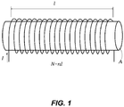
- FIG. 1 An illustration of the operating principle of a conventional inductor device is shown in FIG. 1 .
- a potential difference V that is proportional to a temporal change in current I is generated by electromagnetic induction.
- the most typical inductor element is the coil shown in FIG. 1 .
- B ⁇ H
- Equation (2) if the number of turns n per unit length is constant, the inductance L becomes small in proportion to the volume lA of the inductor element.
- the operating principle in this embodiment utilizes the interaction between the electron spin and the conduction electrons.
- Electrons behave as tiny magnets due to the fact that they have an angular momentum h-bar/2.
- h-bar is the Planck constant h divided by 2n.
- electron spins are the building blocks for the higher-order structure (magnetic structure or magnetic order) that produces the magnetic properties of materials such as ferromagnetism.
- the magnetic order in a material is determined by the arrangement of ordered electron spins (ordered spin), or spin structure.
- the ordered spins that can generate a spin structure are typically spins of localized electrons (localized spins) or spins of conduction electrons when the conduction electrons themselves create a magnetic order.
- the spin structure may take on a parallel spin structure or an anti-parallel spin structure.
- Parallel and anti-parallel spin structures are the origin of ferromagnetic and antiferromagnetic order, respectively, and both are spatially uniform. Spatially uniform structures that are either parallel or antiparallel, such as parallel and antiparallel spin structures, are also called collinear spin structures. On the other hand, it is also known that spin structures with inclination, in which nearby spins are neither parallel nor antiparallel, can be realized in materials, and are called non-collinear spin structures. The inductor elements of the present embodiment are related to this non-collinear spin structure.
- the wavefunction of conduction electrons propagating through the non-collinear spins is affected by the spatial structure of the ordered spins through Hund's coupling, which leads to the spin Berry phase.
- the spin Berry phase acts in the same way as the vector potential of the electromagnetic field.
- the effect of the said spin Berry phase on the conduction electrons can also be described by an electromagnetic field ("emergent electromagnetic fields"), which is a vector potential with an equivalent effect.
- n typically represents a spin structure created by, for example, the spin orientation of localized electrons in a material.
- n has one fixed direction for each position in the xyz Cartesian coordinate system and is time-dependent.
- the subscripts i, j, and k indicate the components of the Cartesian axes x, y, and z, and are chosen cyclically, e i and b i are the components of the emergent electric field and the emergent magnetic field, respectively, and ⁇ i and ⁇ t are the partial derivatives with respect to the spatial coordinate i and the time t, respectively.
- the motion of the conduction electrons is determined according to the superposition of the external electromagnetic field and also the emergent electromagnetic field determined in this way.
- the corresponding voltage drop V in the conduction electrons is given by [Formula 6]
- the current density vector J and the direction of the current-carrying line coincide with each other, and the component of the emergent electric field vector e in this direction is denoted as e, and the length of the line is denoted as 1.
- Non-Patent Documents 1 and 2 for the theory and Non-Patent Document 3 for experimental confirmation.
- Non-Patent Document 4 suggests theoretically that the voltage drop in the helical structure is caused by a deformation of the spin structure of the helical structure by the magnetic field.
- the inventors found that when an electric current is applied to a material with a non-collinear spin structure, an emf will be induced inside the material and the spin structure itself will also be deformed. In addition, we realized that the voltage drop could lead to an operation of inductance rather than simple resistance. In particular, we found that the dependence of the performance on the device size of inductor elements operated in this manner is advantageous for miniaturization.
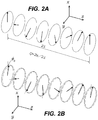
- FIG. 2A shows an arrangement of the ordered spins before an electric current is applied.
- the positions of the ordered spins are fixed, for example, at lattice points (atoms, etc.) not shown in the figure.
- the ordered spin at each position is oriented in plane of a certain plane (xy-plane), and if the orientations are traced perpendicular to the said plane (z-axis orientation), they rotate in the xy-plane in proportion to the distance.
- the ⁇ of the half-turn is the distance required for the spins to flip, which corresponds to the thickness of the magnetic wall dividing the two adjacent magnetic domains in the ferromagnetic order. Since generality will not be lost if the z-axis is defined as the axis of the wavenumber Q of the periodic structure that the helix structure has, the description in this disclosure assumes the Cartesian coordinates in such an orientation.
- Non-Patent Document 2 In a conventional theoretical prediction (Non-Patent Document 2) and experimental observation (Non-Patent Document 3) regarding the generation of a potential difference at the magnetic wall by applying a magnetic field, it has been confirmed that the magnetic wall parallel to the xy plane moves in the z direction under the influence of an external magnetic field, which is oriented perpendicular to the z axis (e.g., x axis) in the helical structure shown in FIG. 2A .
- These disclosures involve only the control of magnetic domains by magnetic fields alone.
- the inventors have found that the voltage drop (Eq. (6)) is efficiently generated by the emergent electric field e (Eq. (4)) in an arrangement where a time-varying alternating current is applied in the z-axis direction, which is the direction of the helix axis.
- e emergent electric field
- the conduction electrons responsible for the current interact with the spin structure.
- One such interaction is the rotational operation that rotates the entire spin structure around the z-axis in FIG. 2A .
- the rotating spin structure itself is deformed by the interaction with the conduction electrons.
- the deformation of the spin structure resulting from the interaction with the conduction electrons i.e., the tilt-up of the ordered spins in the z-axis direction (plane normal direction), is shown in FIG. 2B .
- energy accumulation in the inductor elements of the present embodiment is caused by the tilt-up deformation of the localized spins of the helical structure.
- the conduction electrons which are responsible for the current that causes the energy accumulation, detect the voltage drop caused by the emergent electric field.
- the inductor element 10 has a metal medium 2 having a non-collinear spin structure inside. If the spin structure is a helical structure, the outer shape of the metal medium 2 extends along the z-axis ( FIG. 2A ) so that the current is guided along the z-axis, which is most typically the direction of the wavenumber Q of the helical structure. An electric current I flows through the metal medium 2 in the direction it extends.
- the direction of the electric current I is, more generally, any direction in which the non-collinear spin structure can generate an emergent electric field from the current.
- the localized spins are spatially oriented so that they have a non-collinear spin structure when traced in a certain direction (the z-axis direction in FIG. 3 )
- the outer shape of the metal medium 2 is formed so that the current flowing through it has a projection component along the z-axis direction which gives the non-collinear spin structure.
- FIG 3 depicts, as an example, a structure of an inductor element 10 employing a metal medium 2 where the metal medium 2 has the non-collinear spin structure of the helix structure shown in FIG. 2 , while indicating a representation of the disk 4 containing the spins but omitting the arrows indicating the direction of the spins in FIG. 2 .
- the metal medium 2 has a cross-sectional area A and a length 1, at least locally, and an electric current I flows across this cross-sectional area over the length 1.
- the inductor element 10 is connected to an electric circuit, so the electric current I is the current flowing through the circuit to the inductor element 10.
- the metal medium 2 is depicted as a rectangular shape, but it can take any shape or form as long as the above relationship with the non-collinear spin structure is satisfied; for example, it can be a thin film, film, wiring, or any other pattern and external shape.
- the performance of an inductor element can be evaluated by estimating the degree of deformation of the spin structure caused by the interaction between the conduction electrons and the spin structure.
- the relationship between the deformation of the spin structure and the electric current due to the conduction electrons flowing through it can be analyzed by the equation of motion for the spin structure.
- the vector n which represents the spin structure of the helix shown in FIG.
- n ⁇ e ⁇ 1 cos Qz + ⁇ + e ⁇ 2 sin Qz + ⁇ + m e ⁇ 3 with vectors e 1 , e 2 , and e 3 as unit vectors in each of the xyz Cartesian coordinates.
- the vector n which indicates the orientation of the localized spins, is a vector whose length is 1 at each position, whose orientation is in the xy-plane when m is 0, and whose orientation is determined by z and the magnitude Q of the wavenumber vector of the helix structure.
- the tip of the vector n draws a helix when the vector n is traced along the direction (z-axis) of the wavenumber vector with magnitude Q.
- m is the component of tilt-up in the z-axis direction, which means that it has tilt-up if m is non-zero.
- cos Qz + ⁇ cos Q z ⁇ X
- X reflects ⁇ , which represents the phase of the helix structure that maintains the wavenumber Q, indicating the position of, so to speak, the center of the helicity.
- the determinant D( ⁇ ) becomes [Formula 14]
- D ⁇ ⁇ ⁇ 1 + ⁇ 2 ⁇ 2 + i ⁇ v c ⁇ + v pin ⁇ ⁇ v c ⁇ ⁇ v pin ⁇ .
- ⁇ 0 ⁇ j ⁇ i ⁇ ⁇ ⁇ ⁇ + v pin ⁇ 1 + ⁇ 2 ⁇ 2 + i ⁇ v c ⁇ + v pin ⁇ ⁇ v c ⁇ ⁇ v pin ⁇ .
- Equation (15) is the general form expressing the deformation of the spin structure.
- the performance of the inductor elements is evaluated by estimating the relevant physical quantities by applying the values of the physical parameters of actual materials, realistic values, constant values, etc. to the formulated relational equations.
- the spin anisotropy K ⁇ of intrinsic pinning is about 0.03 K to 2.4 K.
- This intrinsic pinning is the effect of pinning the spins so that they do not tilt-up toward the z-axis, and the anisotropy K ⁇ gives a strength of restoring force.
- This quantity becomes a measure to be overcome for spins to tilt-up.
- this value is the minimum current density required to tilt-up with a direct current (DC)
- AC alternating current
- j int the threshold current density
- ⁇ ⁇ 10 -2 we have v pin ⁇ ⁇ int .
- the dependence of the inductance value on the cross-sectional area A shows that L is proportional to A as shown in Equation (2) in the conventional case, while in the inductor element of the present embodiment L is inversely proportional to A as shown in Equations (31) and (32).
- the inductor device that operates on the principle of this embodiment has an innate property that is extremely favorable to device miniaturization in that L can be increased by reducing the cross-sectional area A.
- the Q value which is the performance index of the inductor element.
- the elevation angle ⁇ 0 is proportional to ⁇ - ⁇ (A-(ii), A-(iii), and B-(iii)). This means that the elevation angle ⁇ 0 remains zero when a specific condition is fulfilled, where the condition is that the damping term ⁇ and the non-adiabatic effect term ⁇ are equal. If the elevation angle ⁇ 0 is not generated, each ordered spin in the spin structure does not try to tilt-up in response to the conduction electron current. In this case, the helical spin structure only moves parallel to the z-axis direction.
- the inductor element in the present embodiment can function equally well by adopting other non-collinear spin structures than a helical structure.
- One such spin structure is the cycloidal structure.
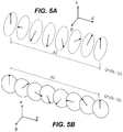
- FIG. 5 the spin structure of the cycloidal structure is shown ( FIG. 5B ) in contrast to the helical structure (also referred to as a proper helix structure, FIG. 5A ).
- the wavenumber of the periodic structure is oriented toward the z-axis while the spins at each position are contained in the xz-plane.
- an elevation angle ⁇ 0 was generated in the direction of the helical axis.
- an elevation angle ⁇ 1 (not shown) is generated from the xz plane to the y-axis direction.
- the voltage drop does not depend on the rotational plane of the spins. This is because the inductance is always in the same direction as the current flowing in the direction of the spin modulation vector, and the voltage appears in the same direction.
- a structure combining a helical structure and a cycloidal structure can be used as an inductor element. For example, in FIG. 3 , considering the multidimensional spin structure, we can combine a helical structure in the z-axis direction and a cycloidal structure in the y-axis direction.
- the spins have a rotational structure with a large wavenumber (short wavelength) when viewed in a certain direction in the zy plane, and when traced in that direction, the spin structure exhibits a rotation in a disk tilted from the direction of the wavenumber vector.
- the inductor element of this embodiment can be operated.
- inductor elements can be implemented in the same manner with materials that form a conical spin structure, where the spins tilt-up from the helix structure with a certain angle of elevation, or a tilted conical spin structure, where the spins are oriented along a conical surface whose conical axis is tilted from the wavenumber direction of the periodic structure.
- Helical structures, cycloidal structures, conical spin structures, tilted conical spin structures, and fan structures are all non-collinear spin structures; moreover, skyrmions, spin structures frustrated in three dimensions, etc. can also be employed to implement the present inductor element.
- FIG. 6 is a scanning electron microscope (SEM) image of a sample of the inductor element 10 in the present embodiment.
- SEM scanning electron microscope
- the rectangular Gd 3 Ru 4 Al 12 was formed on a silicon substrate by the micro-sampling method using a convergent ion beam.
- electrodes 114-128 made of tungsten were formed on both short sides (full width) and both long sides (where a distance of 7 ⁇ m is provided between electrodes on each side) of the metal medium 102.
- Gold thin film wirings 134, 136, 142, 144, 146, and 148 for connection to external circuits are connected to each electrode.
- the gold thin film wirings 134, 136, 142, 144, 146, and 148 were deposited by electron beam deposition and patterned by UV lithography and lift-off methods.
- the electrodes 114-128 were formed by convergent ion beam assisted deposition to connect the gold thin film wirings 134, 136, 142, 144, 146, and 148 to the metal medium 102.
- the short side ones are the drive electrodes 114 and 116 that apply an electric current to the inductor element sample 110, and the long side ones are the probe electrodes 122, 124, 126, and 128 for measuring the voltage drop along the length direction.
- FIG. 7 provides graphs showing the measurement results of the frequency characteristics of the voltage drop of the inductor element sample 110, one with a linear scale ( FIG. 7A ) and one with a logarithmic scale ( FIG. 7B ).
- the vertical axes show the voltage drop (-Im V) appearing in the imaginary part (phase advancement component) of the AC potential difference between the probe electrodes 122 and 124.
- the frequency ⁇ was measured over a range of 0 to 10 kHz
- the AC current applied between the driving electrodes 114 and 116 was set to a current density of 3.3 ⁇ 10 8 A/m 2 .
- the ambient temperature was set at 5 K and 15 K to ensure stability of operation and measurement accuracy.
- the measurement results in FIG7 where a voltage drop proportional to frequency is observed in the frequency range of 0 to 10 kHz, shows that the inductor element sample 110 is actually functioning as an inductance element and that the inductance (L) is substantially constant.
- the size and mass of the inductor element sample 110 is extremely small.
- calculating the mass from the density and volume, based on the density of Gd 3 Ru 4 Al 12 (10.8 g/cm 3 ) and the volume in the sample (approx. 10 ⁇ 20 ⁇ 0.3 ⁇ m 3 ) the size of the metal medium 102 alone, not including the electrodes and substrate, is about 0.65 ng.
- the volume of a conventional inductor element of 130 nH to 270 nH, which is available in the market and disclosed in Non-Patent Document 5, is about 0.6 mm ⁇ 0 .3 mm ⁇ 0.3 mm 54 ⁇ 10 ⁇ 3 mm 3 .
- the inductor element provided in this embodiment can have a similar inductance value with a size and mass of about 10 -6 of that of a conventional inductor element.
- a typical selection criterion is a metallic material that substantially has a ferromagnetic order (roughly parallel order) between adjacent spins, realizes a non-collinear spin structure as a result of modulation from the ferromagnetic order, and exhibits practical electrical conductivity. Examples of non-limiting materials that satisfy these properties are given in Table 1.
- the stacked structure consists of 20 unit structures stacked repeatedly.
- [Pt (3 nm)/Co (0.9 nm)/Ta (4 nm)] 15 is a composite material heterostructure of platinum-based heterostructure with a unit structure of Pt/Co/Ta.
- Each metal layer in the unit structure has the thickness (in nm) in parentheses, and is fabricated in a stacked structure with 15 unit structures repeatedly stacked.
- the lower limits of the domain wall widths of [Ir(10)/Fe(0-6)/Co(4-6)/Pt(10)] 20 and [Pt(3 nm)/Co(0.9 nm)/Ta(4 nm)] 15 are about 80 nm (Non-Patent Document 6) and 90 nm (Non-Patent Document 7), respectively. Therefore, it is expected that the pitch of the helical structure can be shortened to a considerable extent.
- non-collinear spin structure is a spin structure of localized spins that are modulated from the ferromagnetic order by spin-orbit coupling, represented by the Dzyaloshinskii-Moriya interaction, and can be selected from those described above, such as helical structures.
- Such materials can be selected from alloys, typically containing transition metals.
- Materials that realize a non-collinear spin structure among localized spins as a result of the RKKY interaction, which is another generation mechanism than the spin-orbit interaction, can also be employed.
- a non-collinear spin structure can also be realized among localized spins by magnetic frustration, and suitable materials for the inductor device can be selected from such a group of materials.
- the present disclosure also includes apparatus that incorporates electrical and electronic circuits containing the inductor elements described above.
- the inductor elements of the embodiments described above can be employed as basic elements for general electrical and electronic circuits, including, for example, resonant and filter circuits.
- the applicability of the inductor elements described above in principle is not specifically limited, but includes general electrical and electronic equipment including these electronic circuits, and includes electrical and electronic equipment, communication equipment, audio-visual equipment, and medical-related electronic equipment, whether for industrial or home use application. Since the inductor elements provided in the present disclosure can be fabricated in a lightweight and compact package, they can also be applied to hearing aids, cardiac pacemakers, and microelectromechanical systems (MEMS).
- MEMS microelectromechanical systems
- the present disclosure can be used for any device that includes an inductor element in a circuit.
Landscapes
- Engineering & Computer Science (AREA)
- Power Engineering (AREA)
- Microelectronics & Electronic Packaging (AREA)
- Chemical & Material Sciences (AREA)
- Crystallography & Structural Chemistry (AREA)
- Materials Engineering (AREA)
- Coils Or Transformers For Communication (AREA)
- Hall/Mr Elements (AREA)
- Hard Magnetic Materials (AREA)
- Thin Magnetic Films (AREA)
Abstract
Description
- The present disclosure relates to an inductor device and an apparatus comprising the same. More particularly, the present disclosure relates to an inductor element that utilizes a spin structure of electrons and an apparatus comprising the same.
- Among basic electronic devices, basic passive elements in electric circuits that provide a linear relationship between applied voltage and current are typically the R (resistance), C (capacitance), and L (inductance) elements. The physical function of each element is the generation of heat associated with electric current (R), storing energy by electric charge (C), and storing energy by magnetic field (L). Among these, elements responsible for inductance L (inductor elements) in particular have lagged behind in miniaturization. For instance, a product that shows the smallest size with a high inductance value has a size of 0.6 × 0.3 × 0.3 mm3 with inductance value of about L = 130 nH to 270 nH.
- On the other hand, there have been discoveries of physical phenomena with a different operating principle from those of conventional basic electronic elements, which primarily rely on electrons' spin in addition to charge. These physical phenomena are being used in passive devices, active devices, and memory devices. Such a field is sometimes referred to as spintronics, which has shown marked progress these days.
-
- Non-Patent Document 1: Gen Tatara and Hiroshi Kohno, "Theory of Current-Driven Domain Wall Motion: Spin Transfer versus Momentum Transfer," Phys. Rev. Lett. 92, 086601 (2004), DOI: 10.1103/PhysRevLett.92.086601
- Non-Patent Document 2: S. E. Barnes and S. Maekawa, "Generalization of Faraday's Law to Include Nonconservative Spin Forces," Phys. Rev. Lett. 98, 246601 (2007), DOI: 10.1103/PhysRevLett.98.246601
- Non-Patent Document 3: Pham Nam Hai et al., "Electromotive force and huge magnetoresistance in magnetic tunnel junctions," Nature 458, 489-492 (2009) DOI: 10.1038/nature07879
- Non-Patent Document 4: Jun-ichiro Kishine et al., "Coherent sliding dynamics and spin motive force driven by crossed magnetic fields in a chiral helimagnet," Phys. Rev. B 86, 214426 (2012) DOI: 10.1103/PhysRevB.86.214426
- Non-Patent Document 5: LQP03TN_02 series webpage in Murata Manufacturing Co., Ltd. website, [online] last retrieved: July 18, 2019, URL; https://www.murata.com/en-global/products/emiconfun/inductor/2014/02/27/en-20140227-p1
- Non-Patent Document 6: Anjan Soumyanarayanan et al., "Tunable room-temperature magnetic skyrmions in Ir/Fe/Co/Pt multilayers", Nature Materials 16, 898-904 (2017) DOI: 10.1038/nmat4934
- Non-Patent Document 7: Seonghoon Woo et al., "Observation of room-temperature magnetic skyrmions and their current-driven dynamics in ultrathin metallic ferromagnets", Nature Materials 15, 501-506 (2016) DOI: 10.1038/nmat4593
- With the continuing progress in miniaturization of various electronic devices, the demand for miniaturization of various electronic circuit elements remains unabated. In particular, the volume of conventional inductor elements has to be increased in order to gain a higher inductance value. There has been no known operating principle that can realize miniaturization.
- The present disclosure aims to solve at least some of the problems mentioned above. The present disclosure provides a new principle of inductor elements that utilizes the quantum phenomenon observed in the conduction electrons interacting with the spin structure of electrons, thereby contributing to the miniaturization and high density of electronic circuits employing inductor elements and apparatuses containing them.
- The inventors came to the conclusion that it is difficult to miniaturize inductor devices as long as they operate on the principle of conventional inductor devices, i.e., the principle of coupling an electric current to magnetic energy generated within a space or in a magnetic material. Then, we have created a new concept of inductor elements adopting degree of freedom of electrons' spin, and completed the present disclosure.
- That is, in certain aspects of the present disclosure provided is an inductor element comprising a metal medium with a spatially arrangement of ordered spins such that the ordered spins have a non-collinear spin structure when traced in a direction, wherein an electric current is applied through the metal medium in such a way that the electric current has a projection component in the direction.
- The term "inductor element" includes elements and devices also referred to as reactance elements, reactors, etc., unless otherwise noted hereinafter. In addition, due to limitations in the notation of the application document, the term "vector" may be added to the alphabet denoting a variable in the text in place of indicating an arrow above the alphabet. Likewise, due to limitations in notation, the term h-bar may be used in the text to mean the Planck constant h divided by 2n. In addition, due to limitations in notation, academic conventions such as distinguishing variables among constants and variables by italicizing them are not expressed in characters, but only in embedded images. Inconsistencies with conventions due to these restrictions in notation and apparent inconsistencies occurring in written documents shall not affect the disclosure of this disclosure or the interpretation of the scope of rights, as they are caused by constraints imposed on the notation.
- In a certain aspect of the present disclosure, there is provided an inductor element and an electronic device including the same, which are based on a novel operating principle and can be easily miniaturized.
-
-
FIG. 1 is an illustration of the operating principle of a conventional inductor element. -
FIG. 2 provides illustrations of the spin structure of the helix structure proposed in an embodiment of the present disclosure, showing the arrangement of the spins before the electric current is applied (FIG. 2A ) and the rising of the spins perpendicular to the plane as a result of interaction with conduction electrons (FIG. 2B ), respectively. -
FIG. 3 shows a structure showing an example of an inductor element in an embodiment of the present disclosure. -
FIG. 4 provides illustrations of the angles of elevation ϕ0 collectively in each range of angular frequency ω in an embodiment of the present disclosure. -
FIG. 5 provides explanatory illustrations of the non-collinear spin structure in an embodiment of the present disclosure, showing, in contrast to the helical structure (FIG. 5A ), the spin structure of the cycloidal structure (FIG. 5B ). -
FIG. 6 is a SEM (scanning electron microscope) image of a sample of an inductor element in an embodiment of the present disclosure. -
FIG. 7 provides graphs showing the measurement results of the frequency characteristics of the voltage drop of a sample of the inductor element in an embodiment of the present disclosure, one with a linear scale (FIG. 7A ) and one with a logarithmic scale (FIG. 7B ). - Embodiments of the inductor elements of the present disclosure will be described by referring to the following drawings. Throughout the drawings, common parts or elements are denoted by common reference numerals in this description, unless otherwise noted. In addition, each element of each embodiment in the drawing should be understood as not being drawn to scale.
- An illustration of the operating principle of a conventional inductor device is shown in
FIG. 1 . In an inductor element, a potential difference V that is proportional to a temporal change in current I is generated by electromagnetic induction. The relationship can be expressed as follows,
[Formula 1]
FIG. 1 . A material with a large permeability u, such as an iron core, may be placed in the center to increase the magnetic flux density B = µH, and the number of turns N increases the potential difference V in Equation (1). In the coil shown inFIG. 1 , the inductance L is given by the following,
[Formula 2]
- 1-2. Inductance by Interaction between Conduction Electrons and Ordered Spins (Principle)
- In stark contrast to the conventional one, the operating principle in this embodiment utilizes the interaction between the electron spin and the conduction electrons.
- Electrons behave as tiny magnets due to the fact that they have an angular momentum h-bar/2. Here, h-bar is the Planck constant h divided by 2n. Generally speaking, electron spins are the building blocks for the higher-order structure (magnetic structure or magnetic order) that produces the magnetic properties of materials such as ferromagnetism. The magnetic order in a material is determined by the arrangement of ordered electron spins (ordered spin), or spin structure. The ordered spins that can generate a spin structure are typically spins of localized electrons (localized spins) or spins of conduction electrons when the conduction electrons themselves create a magnetic order. The spin structure may take on a parallel spin structure or an anti-parallel spin structure. Parallel and anti-parallel spin structures are the origin of ferromagnetic and antiferromagnetic order, respectively, and both are spatially uniform. Spatially uniform structures that are either parallel or antiparallel, such as parallel and antiparallel spin structures, are also called collinear spin structures. On the other hand, it is also known that spin structures with inclination, in which nearby spins are neither parallel nor antiparallel, can be realized in materials, and are called non-collinear spin structures. The inductor elements of the present embodiment are related to this non-collinear spin structure.
- When the ordered spins have a non-collinear spin structure, the wavefunction of conduction electrons propagating through the non-collinear spins is affected by the spatial structure of the ordered spins through Hund's coupling, which leads to the spin Berry phase. In terms of the effect on the conduction electrons, the spin Berry phase acts in the same way as the vector potential of the electromagnetic field. For this reason, the effect of the said spin Berry phase on the conduction electrons can also be described by an electromagnetic field ("emergent electromagnetic fields"), which is a vector potential with an equivalent effect. We introduce a vector n, which typically represents a spin structure created by, for example, the spin orientation of localized electrons in a material. The vector n has one fixed direction for each position in the xyz Cartesian coordinate system and is time-dependent. The emergent electromagnetic field for describing the effects of the spin structure
[Formula 3]
[Formula 4]
[Formula 5]
[Formula 6]
- It is known that an example that has a non-collinear spin structure and results in a voltage drop is the magnetic wall dividing adjacent magnetic domains, and it has been theoretically investigated and experimentally confirmed that the magnetic wall can be driven by an electric current. The force (electric field) that can explain the voltage drop, such as imparting a potential to the charge, is known as electromotive force (emf). See, e.g.,
Non-Patent Documents Non-Patent Document 3 for experimental confirmation. Another non-collinear spin structure, a helical structure, has also been predicted to produce a voltage drop across the crystalline substance (Non-Patent Document 4).Non-Patent Document 4 suggests theoretically that the voltage drop in the helical structure is caused by a deformation of the spin structure of the helical structure by the magnetic field. - The inventors found that when an electric current is applied to a material with a non-collinear spin structure, an emf will be induced inside the material and the spin structure itself will also be deformed. In addition, we realized that the voltage drop could lead to an operation of inductance rather than simple resistance. In particular, we found that the dependence of the performance on the device size of inductor elements operated in this manner is advantageous for miniaturization.
- The illustrations in
FIG. 2 exemplifies the spin structure of the helical structure proposed in the present embodiment.FIG. 2A shows an arrangement of the ordered spins before an electric current is applied. The positions of the ordered spins are fixed, for example, at lattice points (atoms, etc.) not shown in the figure. At a certain point of time, the ordered spin at each position is oriented in plane of a certain plane (xy-plane), and if the orientations are traced perpendicular to the said plane (z-axis orientation), they rotate in the xy-plane in proportion to the distance. When the orientations of the spins make a full revolution with a period of 2λ, which period is spatial to the orientation of the helix axis, the wavenumber Q of the helix structure can be determined as Q = 2n / (2λ). Note that the λ of the half-turn is the distance required for the spins to flip, which corresponds to the thickness of the magnetic wall dividing the two adjacent magnetic domains in the ferromagnetic order. Since generality will not be lost if the z-axis is defined as the axis of the wavenumber Q of the periodic structure that the helix structure has, the description in this disclosure assumes the Cartesian coordinates in such an orientation. In a conventional theoretical prediction (Non-Patent Document 2) and experimental observation (Non-Patent Document 3) regarding the generation of a potential difference at the magnetic wall by applying a magnetic field, it has been confirmed that the magnetic wall parallel to the xy plane moves in the z direction under the influence of an external magnetic field, which is oriented perpendicular to the z axis (e.g., x axis) in the helical structure shown inFIG. 2A . These disclosures involve only the control of magnetic domains by magnetic fields alone. - The inventors have found that the voltage drop (Eq. (6)) is efficiently generated by the emergent electric field e (Eq. (4)) in an arrangement where a time-varying alternating current is applied in the z-axis direction, which is the direction of the helix axis. When such an electric current is applied, the conduction electrons responsible for the current interact with the spin structure. One such interaction is the rotational operation that rotates the entire spin structure around the z-axis in
FIG. 2A . In addition, the rotating spin structure itself is deformed by the interaction with the conduction electrons. The deformation of the spin structure resulting from the interaction with the conduction electrons, i.e., the tilt-up of the ordered spins in the z-axis direction (plane normal direction), is shown inFIG. 2B . In contrast to the previous inductor elements, in which energy accumulation as magnetic field energy is observed as a voltage drop (Equation (1)), energy accumulation in the inductor elements of the present embodiment is caused by the tilt-up deformation of the localized spins of the helical structure. The conduction electrons, which are responsible for the current that causes the energy accumulation, detect the voltage drop caused by the emergent electric field. - This section describes the configuration of the inductor element of this embodiment. The structure of the inductor element of the present embodiment is shown in
FIG. 3 . Theinductor element 10 has ametal medium 2 having a non-collinear spin structure inside. If the spin structure is a helical structure, the outer shape of themetal medium 2 extends along the z-axis (FIG. 2A ) so that the current is guided along the z-axis, which is most typically the direction of the wavenumber Q of the helical structure. An electric current I flows through themetal medium 2 in the direction it extends. This allows the electric current I to generate an emergent electric field against the ordered spins of the helical structure (more generally, the non-collinear spin structure), which is detected by the conduction electrons responsible for the electric current I. The direction of the electric current I is, more generally, any direction in which the non-collinear spin structure can generate an emergent electric field from the current. For example, if the localized spins are spatially oriented so that they have a non-collinear spin structure when traced in a certain direction (the z-axis direction inFIG. 3 ), the outer shape of themetal medium 2 is formed so that the current flowing through it has a projection component along the z-axis direction which gives the non-collinear spin structure.FIG 3 depicts, as an example, a structure of aninductor element 10 employing ametal medium 2 where themetal medium 2 has the non-collinear spin structure of the helix structure shown inFIG. 2 , while indicating a representation of thedisk 4 containing the spins but omitting the arrows indicating the direction of the spins inFIG. 2 . Themetal medium 2 has a cross-sectional area A and alength 1, at least locally, and an electric current I flows across this cross-sectional area over thelength 1. In general, theinductor element 10 is connected to an electric circuit, so the electric current I is the current flowing through the circuit to theinductor element 10. InFIG. 3 , themetal medium 2 is depicted as a rectangular shape, but it can take any shape or form as long as the above relationship with the non-collinear spin structure is satisfied; for example, it can be a thin film, film, wiring, or any other pattern and external shape. - The performance of an inductor element, such as the inductance value, can be evaluated by estimating the degree of deformation of the spin structure caused by the interaction between the conduction electrons and the spin structure. The relationship between the deformation of the spin structure and the electric current due to the conduction electrons flowing through it can be analyzed by the equation of motion for the spin structure. The vector n, which represents the spin structure of the helix shown in
FIG. 2A , is determined only by z in xyz Cartesian coordinates and is written as
[Formula 7]
[Formula 8]
Additionally, taking into account the interaction with the electric current by the conduction electrons, the equation of motion for the spin structure is given by the following equations, where ϕ0 is the angle of elevation of the spin from the xy-plane to the z-direction
[Formula 9]
[Formula 10]
[Formula 11]
[Formula 12]
[Formula 13]
[Formula 14]
[Formula 15]
- jint: threshold current density due to intrinsic pinning

- jpin: threshold current density due to extrinsic pinning


[Formula 16]
- Next, we divide into cases in terms of the relationship between vpin and νint, and investigate how the value of elevation angle ϕ0 is expressed for each range of values of ω (the time-dependent angular frequency of elevation angle ϕ0). The results can be easily understood by dividing them into two cases, Cases A and B, in terms of νpin and νint, and then dividing each case in terms of the value of angular frequency ω (six cases in total). At this point, it is assumed that vpin « vint as α, β « 1. Therefore, the denominator of the right-hand side of Equation (16) is reduced to ≈
ω 2+iαωνint-νpinνint. The "Denominator" and "Numerator" in this and other cases are those in the right-hand side of Equation (16) unless otherwise noted. - (A)

- A- (i)


Then, we have
[Formula 17]
- A- (ii) νpin / α << ω << νint
In this case, we have
[Formula 18]
- A- (iii) νint << ω
In this case, we have
[Formula 19]
- A- (i)
- (B) ανint << νpin << νint
- B-(i) ω<< ανint << νpin << νint
In this case

[Formula 20]
- B-(ii) ανint << ω << (νpin νint)1/2
In this case,

Then, we have
[Formula 21]
- B-(iii) (νpin νint)1/2 << ω << νint
In this case, we have
Denominator: ω2
Numerator:
therefore, Numerator ≈ iω(β-α)
Thus, we have
[Formula 22]
- B-(i) ω<< ανint << νpin << νint
- To classify the emergent electric field in terms of the helical spin structure, we can calculate Equation (4) for the spin field structure shown in Equation (6). Since
[Formula 23]
[Formula 24]
[Formula 25]
- The performance of the inductor elements is evaluated by estimating the relevant physical quantities by applying the values of the physical parameters of actual materials, realistic values, constant values, etc. to the formulated relational equations.
- The spin anisotropy K⊥ of intrinsic pinning is about 0.03 K to 2.4 K. This intrinsic pinning is the effect of pinning the spins so that they do not tilt-up toward the z-axis, and the anisotropy K⊥ gives a strength of restoring force. This quantity becomes a measure to be overcome for spins to tilt-up. Based on the relationship between

- By substituting the partial derivative over time in Equation (25) with each frequency and taking its real part, ez can be expressed as
[Formula 26]
- λ = 20 nm = 2 × 10⁻⁸ m
- e = 1.6 × 10⁻¹⁹ C
- h-bar = 10-31 J·sec,
- Furthermore, when the length of the sample is 1 = 1 mm and the current density J = 109 A/m2, the voltage is

- Next, we estimate the values of νint and νpin. For one of them, νint, assuming a material with the conduction properties of a common metal, we have the localized spin of magnitude S∼1, the electron density n, and the lattice constant a as na3 ∼ 1, and the threshold current density jint ∼ 1012 A/m2, to obtain the following:

Let P = 0.1 and a = 4 nm, we get
[Formula 28]

- For the other one, νpin, assuming jpin = 1010 A/m, we have
[Formula 29]
- Next, we will explain the characteristics of the inductor element. We make an estimation of inductance L for a linear conductor of cross-sectional area A and
length 1, whose direction of extension is aligned with the wavenumber direction of the helical structure (FIG. 3 ). In Equation (1), V = l ez, current value I = j A, and
[Formula 30]
[Formula 31]
[Formula 32]

- This value of L is about 1/400 of the value of the existing device described above (L = 130 nH to 270 nH approx.). What is completely different from the conventional one in this regard is a scaling law concerning the size of the inductor element itself. The dependence of the inductance value on the cross-sectional area A shows that L is proportional to A as shown in Equation (2) in the conventional case, while in the inductor element of the present embodiment L is inversely proportional to A as shown in Equations (31) and (32). In other words, the inductor device that operates on the principle of this embodiment has an innate property that is extremely favorable to device miniaturization in that L can be increased by reducing the cross-sectional area A.
- In order to predict the performance of the inductor element, we further calculate the Q value, which is the performance index of the inductor element.
- Since
- Q = Lω / R = 2 n L v / R, and
- R = ρl / A,
- By substituting jint = 1012 A/m and λ = 20 nm = 2 × 10⁻⁸ m and other values into the above, we obtain Q ∼ 0.3 × 10⁻⁸ v/p (sec-1/µΩ cm). For ρ ∼ 1 µΩ cm and ν ∼ 109 sec-1, we can obtain a value of about Q ∼ 3, which predicts that the inductor element in the present embodiment can actually function as an inductor element. In general, a good conductor with small p and a material with small λ (i.e., small helical pitch of the spin structure) is suitable for increasing Q.
- Returning to
FIG. 4 , we explain some of the findings for the elevation angle ϕ0. How the elevation angle ϕ0 behaves with respect to the angular frequency ω is shown inFIG. 4 . When the angular frequency ω in the temporal term is small and the operation is close to DC, the ratio of the intrinsic pinning of the current density j to the threshold current density jint determines the scale of the elevation angle ϕ0 in both Cases A and B. This is the reason why the threshold current density jint is important in DC. However, the threshold current density jint is rather irrelevant at high frequencies. There are also cases where the elevation angle ϕ0 is proportional to β - α (A-(ii), A-(iii), and B-(iii)). This means that the elevation angle ϕ0 remains zero when a specific condition is fulfilled, where the condition is that the damping term α and the non-adiabatic effect term β are equal. If the elevation angle ϕ0 is not generated, each ordered spin in the spin structure does not try to tilt-up in response to the conduction electron current. In this case, the helical spin structure only moves parallel to the z-axis direction. Note that a simple rotation of the helix structure about the z-axis cannot be distinguished from a translation of the helix structure itself along the z-axis for any value of the elevation angle, therefore they are considered identical. Also, if no elevation angle ϕ0 is generated, inductance is not generated. However, since β ≠ α can be assumed in the actual spin structure, it can be fully expected that the elevation angle ϕ0 is generated and that inductance is also generated. - The inductor element in the present embodiment can function equally well by adopting other non-collinear spin structures than a helical structure. One such spin structure is the cycloidal structure. In
FIG. 5 , the spin structure of the cycloidal structure is shown (FIG. 5B ) in contrast to the helical structure (also referred to as a proper helix structure,FIG. 5A ). - In a typical cycloidal structure, the wavenumber of the periodic structure is oriented toward the z-axis while the spins at each position are contained in the xz-plane. As mentioned above, as a result of the spin Berry phase acted on the conduction electrons in the helical structure (Proper Helix structure), an elevation angle ϕ0 was generated in the direction of the helical axis. In contrast to that, in the cycloidal structure, when an electric current is applied in the z-axis direction, an elevation angle ϕ1 (not shown) is generated from the xz plane to the y-axis direction. This is because the cycloidal structure can be described by the same equation in which the components of the unit vector e2 and e3 are interchanged in Equations (6), (23), and (24) for the helical structure described above, and because an emergent electric field ez proportional to the component of the unit vector e2, i.e., the elevation angle ϕ1, is generated as well. In this way, the properties established for the helix structure (proper helix structure) are also found in the case of the cycloidal structure shown in
FIG. 5B . The same is true for the estimation of each value. - It should be noted that the voltage drop does not depend on the rotational plane of the spins. This is because the inductance is always in the same direction as the current flowing in the direction of the spin modulation vector, and the voltage appears in the same direction. Also, a structure combining a helical structure and a cycloidal structure can be used as an inductor element. For example, in
FIG. 3 , considering the multidimensional spin structure, we can combine a helical structure in the z-axis direction and a cycloidal structure in the y-axis direction. In such a configuration, the spins have a rotational structure with a large wavenumber (short wavelength) when viewed in a certain direction in the zy plane, and when traced in that direction, the spin structure exhibits a rotation in a disk tilted from the direction of the wavenumber vector. When the current is applied in the direction where rotation of the spin direction can be traced (the direction in which electrons sense the non-collinear spin structure), including such structures mentioned above as well as helical and cycloidal structures, the inductor element of this embodiment can be operated. - Even if the structure is not a helical or cycloidal structure, a fan structure, in which the spins swing left and right to form a fan, will in principle exhibit the same phenomenon as in the case of a helical structure. Furthermore, since the same inductance does not cause sign reversal in either of the crystal helicities (right-handed or left-handed systems), there is no need to fabricate the metal medium so that it has a single-domain structure with matching helicities of ordered spins.
- In addition, other non-collinear spin structures can also be employed for this implementation of inductor elements. For example, inductor elements can be implemented in the same manner with materials that form a conical spin structure, where the spins tilt-up from the helix structure with a certain angle of elevation, or a tilted conical spin structure, where the spins are oriented along a conical surface whose conical axis is tilted from the wavenumber direction of the periodic structure. Helical structures, cycloidal structures, conical spin structures, tilted conical spin structures, and fan structures are all non-collinear spin structures; moreover, skyrmions, spin structures frustrated in three dimensions, etc. can also be employed to implement the present inductor element.
- Following the filing of basic application of this disclosure application, the inventors conducted an experimental demonstration of the operation of the inductor element proposed in this embodiment as a research theme adopted by the Japan Science and Technology Agency's Core Research for Evolutionary Science and Technology (CREST) program in 2018.
FIG. 6 is a scanning electron microscope (SEM) image of a sample of theinductor element 10 in the present embodiment. In theinductor element sample 110, a thin film of Gd3 Ru4 Al12 with a thickness of 0.3 µm was formed into a rectangle with a width of 10 µm and a length of 20 µm, which was used as themetal medium 102. Specifically, the rectangular Gd3 Ru4 Al12 was formed on a silicon substrate by the micro-sampling method using a convergent ion beam. In addition, electrodes 114-128 made of tungsten were formed on both short sides (full width) and both long sides (where a distance of 7 µm is provided between electrodes on each side) of themetal medium 102. Goldthin film wirings thin film wirings thin film wirings metal medium 102. The short side ones are thedrive electrodes inductor element sample 110, and the long side ones are theprobe electrodes - What is to be measured is the voltage drop between the
probe electrodes probe electrodes drive electrodes -
FIG. 7 provides graphs showing the measurement results of the frequency characteristics of the voltage drop of theinductor element sample 110, one with a linear scale (FIG. 7A ) and one with a logarithmic scale (FIG. 7B ). In both graphs, the horizontal axes show the frequency ν (= ω/2π) of the applied sine wave AC current, and the vertical axes show the voltage drop (-Im V) appearing in the imaginary part (phase advancement component) of the AC potential difference between theprobe electrodes electrodes - In general, the voltage drop V follows the relation

FIG7 , where a voltage drop proportional to frequency is observed in the frequency range of 0 to 10 kHz, shows that theinductor element sample 110 is actually functioning as an inductance element and that the inductance (L) is substantially constant. - If we use a measured value at a temperature of 5 K shown in
FIG. 7B to calculate the value of inductance L, i.e., Im V = 5 µV (value at a frequency of 10 kHz), the inductance value L can be valued at about 0.08 µH for a current density = 3.3 × 10⁸ A/m2, or about 80 nH. - The size and mass of the
inductor element sample 110 is extremely small. The effective volume of themetal medium 102 of the above sample, taking into account the distance between electrodes, is 0.3 µm × 10 µm × 7 µm = 21 × 10-9 mm3 and its mass is 1n grams, or less than 10-9 g. Specifically, calculating the mass from the density and volume, based on the density of Gd3 Ru4 Al12 (10.8 g/cm3) and the volume in the sample (approx. 10 × 20 × 0.3 µm3), the size of themetal medium 102 alone, not including the electrodes and substrate, is about 0.65 ng. - The volume of a conventional inductor element of 130 nH to 270 nH, which is available in the market and disclosed in
Non-Patent Document 5, is about
- Next, we will explain materials that can realize the non-collinear spin structure and operate as the inductor element of the present embodiment. From the above explanation, a typical selection criterion is a metallic material that substantially has a ferromagnetic order (roughly parallel order) between adjacent spins, realizes a non-collinear spin structure as a result of modulation from the ferromagnetic order, and exhibits practical electrical conductivity. Examples of non-limiting materials that satisfy these properties are given in Table 1.
[Table 1] Alloy Composition/ Composition Formula Spin Structure MnSi Helix Structure, Skyrmion Structure Fe(Ge,Si) Helix Structure, Skyrmion Structure Co-Zn-Mn (Co8Zn8Mn4) Helix Structure, Skyrmion Structure (Fe,Co)Si Helix Structure, Skyrmion Structure Mn(Ge,Si) Helix Structure, Skyrmion Structure YbNi3Al6 Helix Structure CeRhIn5 Helix Structure Gd3Ru4Al12 Helix Structure, Skyrmion Structure [Ir(10)/Fe(0-6)/Co(4-6)/Pt(10)]20 Helix Structure, Skyrmion Structure [Pt(3nm)/Co(0.9nm)/Ta(4nm)]15 Helix Structure, Skyrmion Structure - In general, materials with a non-collinear spin structure can be employed in the present embodiment. The non-collinear spin structure is a spin structure of localized spins that are modulated from the ferromagnetic order by spin-orbit coupling, represented by the Dzyaloshinskii-Moriya interaction, and can be selected from those described above, such as helical structures. Such materials can be selected from alloys, typically containing transition metals. Materials that realize a non-collinear spin structure among localized spins as a result of the RKKY interaction, which is another generation mechanism than the spin-orbit interaction, can also be employed. In addition, a non-collinear spin structure can also be realized among localized spins by magnetic frustration, and suitable materials for the inductor device can be selected from such a group of materials.
- The present disclosure also includes apparatus that incorporates electrical and electronic circuits containing the inductor elements described above. The inductor elements of the embodiments described above can be employed as basic elements for general electrical and electronic circuits, including, for example, resonant and filter circuits. The applicability of the inductor elements described above in principle is not specifically limited, but includes general electrical and electronic equipment including these electronic circuits, and includes electrical and electronic equipment, communication equipment, audio-visual equipment, and medical-related electronic equipment, whether for industrial or home use application. Since the inductor elements provided in the present disclosure can be fabricated in a lightweight and compact package, they can also be applied to hearing aids, cardiac pacemakers, and microelectromechanical systems (MEMS).
- In the above description, the embodiment of the present disclosure has been described specifically. Any description in this Specification is for the purpose of explaining the present disclosure, therefore the scope of the invention of this disclosure should be determined based on recitations of the claims. Furthermore, other variation based on any combination of the embodiment is included in the present disclosure, which variation should be also within a scope of the claims.
- The present disclosure can be used for any device that includes an inductor element in a circuit.
-
- 10
- inductor element
- 2
- metal medium
- 4
- disks (showing non-collinear spin structure)
- 110
- inductor element sample
- 102
- metal medium
- 114, 116, 122, 124, 126, 128
- electrodes
- 134, 136, 142, 144, 146, 148
- gold thin film wiring
[Formula 27]

[Formula 33]

Claims (5)
- An inductor element comprising a metal medium with a spatially arrangement of ordered spins such that the ordered spins have a non-collinear spin structure when traced in a direction, wherein an electric current is applied through the metal medium in such a way that the electric current has a projection component in the direction.
- The inductor element according to claim 1, wherein the metal medium is a material with the spatial arrangement of a helical structure whose wave vector direction is aligned with the direction.
- The inductor element according to claim 1, wherein the metal medium is a material with the spatial arrangement of a cycloidal structure whose wave vector direction is aligned with the direction.
- The inductor element according to claim 1, wherein the metal medium is a material with a ferromagnetic order in which the adjacent ordered spins are substantially ferromagnetic.
- An apparatus comprising an inductor element according to claim 1.
Applications Claiming Priority (2)
| Application Number | Priority Date | Filing Date | Title |
|---|---|---|---|
| JP2018145483 | 2018-08-01 | ||
| PCT/JP2019/030236 WO2020027268A1 (en) | 2018-08-01 | 2019-08-01 | Inductor element and apparatus including same |
Publications (3)
| Publication Number | Publication Date |
|---|---|
| EP3832676A1 true EP3832676A1 (en) | 2021-06-09 |
| EP3832676A4 EP3832676A4 (en) | 2022-05-04 |
| EP3832676B1 EP3832676B1 (en) | 2025-04-23 |
Family
ID=69231157
Family Applications (1)
| Application Number | Title | Priority Date | Filing Date |
|---|---|---|---|
| EP19844237.8A Active EP3832676B1 (en) | 2018-08-01 | 2019-08-01 | Inductor element and apparatus including same |
Country Status (5)
| Country | Link |
|---|---|
| US (1) | US12362085B2 (en) |
| EP (1) | EP3832676B1 (en) |
| JP (1) | JP7385283B2 (en) |
| CN (1) | CN112514012B (en) |
| WO (1) | WO2020027268A1 (en) |
Families Citing this family (8)
| Publication number | Priority date | Publication date | Assignee | Title |
|---|---|---|---|---|
| JP7560871B2 (en) * | 2021-02-03 | 2024-10-03 | 国立研究開発法人理化学研究所 | Inductor element and device including same |
| JP7580068B2 (en) * | 2021-02-26 | 2024-11-11 | 国立研究開発法人日本原子力研究開発機構 | Thin-film inductor element and thin-film variable inductor element |
| WO2023238334A1 (en) * | 2022-06-09 | 2023-12-14 | Tdk株式会社 | Spin inductor |
| CN118120034A (en) * | 2022-09-30 | 2024-05-31 | Tdk株式会社 | Spin Inductor |
| US20260179818A1 (en) * | 2023-07-04 | 2026-06-25 | Tdk Corporation | Spin inductor |
| CN118841235B (en) * | 2024-07-11 | 2025-05-06 | 南京大学 | Coilless proton inductor, design method and control method |
| WO2026033583A1 (en) * | 2024-08-05 | 2026-02-12 | Tdk株式会社 | Spin inductor |
| WO2026033584A1 (en) * | 2024-08-05 | 2026-02-12 | Tdk株式会社 | Spin inductor |
Family Cites Families (13)
| Publication number | Priority date | Publication date | Assignee | Title |
|---|---|---|---|---|
| JP4690675B2 (en) * | 2004-07-30 | 2011-06-01 | 株式会社東芝 | Magnetoresistive element, magnetic head, and magnetic recording / reproducing apparatus |
| JP2011508415A (en) * | 2007-12-21 | 2011-03-10 | コーニンクレッカ フィリップス エレクトロニクス エヌ ヴィ | Electromagnet having superconducting film and laminated ferromagnetic core for suppressing eddy magnetic field |
| DE102009021400A1 (en) * | 2009-05-14 | 2010-11-18 | Forschungszentrum Jülich GmbH | Magnetoelectronic components and measuring methods |
| WO2015118579A1 (en) | 2014-02-10 | 2015-08-13 | 独立行政法人理化学研究所 | Skyrmion drive method |
| JP6450389B2 (en) * | 2014-08-07 | 2019-01-09 | 国立研究開発法人理化学研究所 | Magnetic storage medium and data recording apparatus |
| WO2016158230A1 (en) * | 2015-03-31 | 2016-10-06 | 国立研究開発法人科学技術振興機構 | Skyrmion generation device, skyrmion generation method, and magnetic memory device |
| US9773540B2 (en) * | 2015-07-17 | 2017-09-26 | The Johns Hopkins University | Skyrmion based universal memory operated by electric current |
| CL2015003361A1 (en) * | 2015-11-16 | 2017-08-04 | Univ Santiago Chile | Alternate magnetic field nanogenerator that uses a nanowire that allows it to be applied in the alternating current generation at the nanoscale level; and associated method |
| US9899071B2 (en) * | 2016-01-20 | 2018-02-20 | The Johns Hopkins University | Heavy metal multilayers for switching of magnetic unit via electrical current without magnetic field, method and applications |
| US20170260634A1 (en) * | 2016-01-29 | 2017-09-14 | John Timothy Sullivan | Enhanced Exothermic Reaction (EER) Reactor |
| WO2017222588A1 (en) * | 2016-06-21 | 2017-12-28 | Intel Corporation | In-plane current driven magnetic skyrmion spin oscillator |
| US11557719B2 (en) * | 2018-02-06 | 2023-01-17 | Tohoku University | Magnetoresistance effect element, circuit device, and circuit unit |
| GB201806425D0 (en) * | 2018-04-20 | 2018-06-06 | Provost Fellows Found Scholars And The Other Members Of Board Of The College Of The Holy And Undivid | Single magnetic-layer microwave oscillator |
-
2019
- 2019-08-01 EP EP19844237.8A patent/EP3832676B1/en active Active
- 2019-08-01 WO PCT/JP2019/030236 patent/WO2020027268A1/en not_active Ceased
- 2019-08-01 JP JP2020534743A patent/JP7385283B2/en active Active
- 2019-08-01 CN CN201980050902.7A patent/CN112514012B/en active Active
- 2019-08-01 US US17/264,510 patent/US12362085B2/en active Active
Also Published As
| Publication number | Publication date |
|---|---|
| US12362085B2 (en) | 2025-07-15 |
| EP3832676B1 (en) | 2025-04-23 |
| CN112514012A (en) | 2021-03-16 |
| WO2020027268A1 (en) | 2020-02-06 |
| JPWO2020027268A1 (en) | 2021-09-09 |
| JP7385283B2 (en) | 2023-11-22 |
| CN112514012B (en) | 2024-03-08 |
| US20210383955A1 (en) | 2021-12-09 |
| EP3832676A4 (en) | 2022-05-04 |
Similar Documents
| Publication | Publication Date | Title |
|---|---|---|
| EP3832676B1 (en) | Inductor element and apparatus including same | |
| Qin et al. | Room-temperature magnetoresistance in an all-antiferromagnetic tunnel junction | |
| Yamada et al. | A metallic p-wave magnet with commensurate spin helix | |
| Hervé et al. | Stabilizing spin spirals and isolated skyrmions at low magnetic field exploiting vanishing magnetic anisotropy | |
| Niimi et al. | Reciprocal spin Hall effects in conductors with strong spin–orbit coupling: a review | |
| Cao et al. | Switchable anomalous Hall effects in polar-stacked 2D antiferromagnet MnBi2Te4 | |
| Qin et al. | Anomalous Hall effect, robust negative magnetoresistance, and memory devices based on a noncollinear antiferromagnetic metal | |
| EP3312841A1 (en) | Magnetic tunnel junction device and magnetic memory device | |
| Strigl et al. | Emerging magnetic order in platinum atomic contacts and chains | |
| JP7055480B2 (en) | Low power terahertz magnetic nanooscillator | |
| Huang et al. | Layer-dependent magnetism and spin fluctuations in atomically thin van der Waals magnet CrPS4 | |
| Zhang et al. | Room-temperature highly-tunable coercivity and highly-efficient multi-states magnetization switching by small current in single 2D ferromagnet Fe3GaTe2 | |
| Göbel et al. | Topological orbital Hall effect caused by skyrmions and antiferromagnetic skyrmions | |
| Han et al. | Harnessing magnetic octupole Hall effect to induce torque in altermagnets | |
| Zhang et al. | Lifshitz transition and anisotropic plasmons in altermagnetic two-dimensional Cairo pentagonal metal-organic frameworks | |
| Kobs | Magnetogalvanic effects in ferromagnets of reduced dimensions | |
| Zheng et al. | Crystal-orientation-modulated exchange bias in orthorhombic-ymno3/la0. 6sr0. 4mno3 multiferroic heterostructures | |
| Li et al. | Magnetization switching by asymmetric topological surfaces | |
| Chen et al. | Giant room-temperature third-order electrical transport in a thin-film altermagnet candidate | |
| Yu et al. | Observation of unconventional spin-polarization induced spin–orbit torque in L12-ordered antiferromagnetic Mn3Pt thin films | |
| Smorka et al. | Nonequilibrium dynamics in a spin valve with noncollinear magnetization | |
| Wu et al. | Enhancement of damping-like field and field-free switching in Pt/(Co/Pt)/PtMn trilayer films prepared in the presence of an in situ magnetic field | |
| Qin et al. | A quantitative Arrott analysis methodology for magnetic susceptibility of microscale ferromagnetic nanoflakes | |
| Wen et al. | Competition between Electronic and Magnonic Spin Currents in Metallic Antiferromagnets | |
| Shi et al. | Emergence of room temperature magnetotransport anomaly in epitaxial Pt/γ′-Fe4N/MgO heterostructures toward noncollinear spintronics |
Legal Events
| Date | Code | Title | Description |
|---|---|---|---|
| STAA | Information on the status of an ep patent application or granted ep patent |
Free format text: STATUS: THE INTERNATIONAL PUBLICATION HAS BEEN MADE |
|
| PUAI | Public reference made under article 153(3) epc to a published international application that has entered the european phase |
Free format text: ORIGINAL CODE: 0009012 |
|
| STAA | Information on the status of an ep patent application or granted ep patent |
Free format text: STATUS: REQUEST FOR EXAMINATION WAS MADE |
|
| 17P | Request for examination filed |
Effective date: 20210215 |
|
| AK | Designated contracting states |
Kind code of ref document: A1 Designated state(s): AL AT BE BG CH CY CZ DE DK EE ES FI FR GB GR HR HU IE IS IT LI LT LU LV MC MK MT NL NO PL PT RO RS SE SI SK SM TR |
|
| DAV | Request for validation of the european patent (deleted) | ||
| DAX | Request for extension of the european patent (deleted) | ||
| A4 | Supplementary search report drawn up and despatched |
Effective date: 20220407 |
|
| RIC1 | Information provided on ipc code assigned before grant |
Ipc: H01L 29/82 20060101ALI20220401BHEP Ipc: H01F 17/00 20060101ALI20220401BHEP Ipc: H01F 1/00 20060101ALI20220401BHEP Ipc: B82Y 25/00 20110101ALI20220401BHEP Ipc: H01F 10/32 20060101AFI20220401BHEP |
|
| STAA | Information on the status of an ep patent application or granted ep patent |
Free format text: STATUS: EXAMINATION IS IN PROGRESS |
|
| 17Q | First examination report despatched |
Effective date: 20240326 |
|
| GRAP | Despatch of communication of intention to grant a patent |
Free format text: ORIGINAL CODE: EPIDOSNIGR1 |
|
| STAA | Information on the status of an ep patent application or granted ep patent |
Free format text: STATUS: GRANT OF PATENT IS INTENDED |
|
| RIC1 | Information provided on ipc code assigned before grant |
Ipc: H01L 29/82 20060101ALI20241105BHEP Ipc: H01F 10/193 20060101ALI20241105BHEP Ipc: H01F 17/00 20060101ALI20241105BHEP Ipc: H01F 10/32 20060101AFI20241105BHEP |
|
| INTG | Intention to grant announced |
Effective date: 20241115 |
|
| GRAS | Grant fee paid |
Free format text: ORIGINAL CODE: EPIDOSNIGR3 |
|
| GRAA | (expected) grant |
Free format text: ORIGINAL CODE: 0009210 |
|
| STAA | Information on the status of an ep patent application or granted ep patent |
Free format text: STATUS: THE PATENT HAS BEEN GRANTED |
|
| AK | Designated contracting states |
Kind code of ref document: B1 Designated state(s): AL AT BE BG CH CY CZ DE DK EE ES FI FR GB GR HR HU IE IS IT LI LT LU LV MC MK MT NL NO PL PT RO RS SE SI SK SM TR |
|
| REG | Reference to a national code |
Ref country code: GB Ref legal event code: FG4D |
|
| REG | Reference to a national code |
Ref country code: CH Ref legal event code: EP |
|
| REG | Reference to a national code |
Ref country code: DE Ref legal event code: R096 Ref document number: 602019069103 Country of ref document: DE |
|
| REG | Reference to a national code |
Ref country code: IE Ref legal event code: FG4D |
|
| REG | Reference to a national code |
Ref country code: NL Ref legal event code: MP Effective date: 20250423 |
|
| PG25 | Lapsed in a contracting state [announced via postgrant information from national office to epo] |
Ref country code: NL Free format text: LAPSE BECAUSE OF FAILURE TO SUBMIT A TRANSLATION OF THE DESCRIPTION OR TO PAY THE FEE WITHIN THE PRESCRIBED TIME-LIMIT Effective date: 20250423 |
|
| REG | Reference to a national code |
Ref country code: AT Ref legal event code: MK05 Ref document number: 1788638 Country of ref document: AT Kind code of ref document: T Effective date: 20250423 |
|
| PG25 | Lapsed in a contracting state [announced via postgrant information from national office to epo] |
Ref country code: PT Free format text: LAPSE BECAUSE OF FAILURE TO SUBMIT A TRANSLATION OF THE DESCRIPTION OR TO PAY THE FEE WITHIN THE PRESCRIBED TIME-LIMIT Effective date: 20250825 Ref country code: FI Free format text: LAPSE BECAUSE OF FAILURE TO SUBMIT A TRANSLATION OF THE DESCRIPTION OR TO PAY THE FEE WITHIN THE PRESCRIBED TIME-LIMIT Effective date: 20250423 Ref country code: ES Free format text: LAPSE BECAUSE OF FAILURE TO SUBMIT A TRANSLATION OF THE DESCRIPTION OR TO PAY THE FEE WITHIN THE PRESCRIBED TIME-LIMIT Effective date: 20250423 |
|
| PGFP | Annual fee paid to national office [announced via postgrant information from national office to epo] |
Ref country code: DE Payment date: 20250820 Year of fee payment: 7 |
|
| REG | Reference to a national code |
Ref country code: LT Ref legal event code: MG9D |
|
| PG25 | Lapsed in a contracting state [announced via postgrant information from national office to epo] |
Ref country code: NO Free format text: LAPSE BECAUSE OF FAILURE TO SUBMIT A TRANSLATION OF THE DESCRIPTION OR TO PAY THE FEE WITHIN THE PRESCRIBED TIME-LIMIT Effective date: 20250723 Ref country code: GR Free format text: LAPSE BECAUSE OF FAILURE TO SUBMIT A TRANSLATION OF THE DESCRIPTION OR TO PAY THE FEE WITHIN THE PRESCRIBED TIME-LIMIT Effective date: 20250724 |
|
| PG25 | Lapsed in a contracting state [announced via postgrant information from national office to epo] |
Ref country code: PL Free format text: LAPSE BECAUSE OF FAILURE TO SUBMIT A TRANSLATION OF THE DESCRIPTION OR TO PAY THE FEE WITHIN THE PRESCRIBED TIME-LIMIT Effective date: 20250423 |
|
| PG25 | Lapsed in a contracting state [announced via postgrant information from national office to epo] |
Ref country code: BG Free format text: LAPSE BECAUSE OF FAILURE TO SUBMIT A TRANSLATION OF THE DESCRIPTION OR TO PAY THE FEE WITHIN THE PRESCRIBED TIME-LIMIT Effective date: 20250423 |
|
| PGFP | Annual fee paid to national office [announced via postgrant information from national office to epo] |
Ref country code: GB Payment date: 20250820 Year of fee payment: 7 |
|
| PG25 | Lapsed in a contracting state [announced via postgrant information from national office to epo] |
Ref country code: HR Free format text: LAPSE BECAUSE OF FAILURE TO SUBMIT A TRANSLATION OF THE DESCRIPTION OR TO PAY THE FEE WITHIN THE PRESCRIBED TIME-LIMIT Effective date: 20250423 |
|
| PG25 | Lapsed in a contracting state [announced via postgrant information from national office to epo] |
Ref country code: AT Free format text: LAPSE BECAUSE OF FAILURE TO SUBMIT A TRANSLATION OF THE DESCRIPTION OR TO PAY THE FEE WITHIN THE PRESCRIBED TIME-LIMIT Effective date: 20250423 |
|
| PGFP | Annual fee paid to national office [announced via postgrant information from national office to epo] |
Ref country code: FR Payment date: 20250828 Year of fee payment: 7 |
|
| PG25 | Lapsed in a contracting state [announced via postgrant information from national office to epo] |
Ref country code: RS Free format text: LAPSE BECAUSE OF FAILURE TO SUBMIT A TRANSLATION OF THE DESCRIPTION OR TO PAY THE FEE WITHIN THE PRESCRIBED TIME-LIMIT Effective date: 20250723 |
|
| PG25 | Lapsed in a contracting state [announced via postgrant information from national office to epo] |
Ref country code: IS Free format text: LAPSE BECAUSE OF FAILURE TO SUBMIT A TRANSLATION OF THE DESCRIPTION OR TO PAY THE FEE WITHIN THE PRESCRIBED TIME-LIMIT Effective date: 20250823 |
|
| PG25 | Lapsed in a contracting state [announced via postgrant information from national office to epo] |
Ref country code: LV Free format text: LAPSE BECAUSE OF FAILURE TO SUBMIT A TRANSLATION OF THE DESCRIPTION OR TO PAY THE FEE WITHIN THE PRESCRIBED TIME-LIMIT Effective date: 20250423 |
|
| PG25 | Lapsed in a contracting state [announced via postgrant information from national office to epo] |
Ref country code: SM Free format text: LAPSE BECAUSE OF FAILURE TO SUBMIT A TRANSLATION OF THE DESCRIPTION OR TO PAY THE FEE WITHIN THE PRESCRIBED TIME-LIMIT Effective date: 20250423 Ref country code: DK Free format text: LAPSE BECAUSE OF FAILURE TO SUBMIT A TRANSLATION OF THE DESCRIPTION OR TO PAY THE FEE WITHIN THE PRESCRIBED TIME-LIMIT Effective date: 20250423 |
|
| PG25 | Lapsed in a contracting state [announced via postgrant information from national office to epo] |
Ref country code: CZ Free format text: LAPSE BECAUSE OF FAILURE TO SUBMIT A TRANSLATION OF THE DESCRIPTION OR TO PAY THE FEE WITHIN THE PRESCRIBED TIME-LIMIT Effective date: 20250423 |
|
| PG25 | Lapsed in a contracting state [announced via postgrant information from national office to epo] |
Ref country code: EE Free format text: LAPSE BECAUSE OF FAILURE TO SUBMIT A TRANSLATION OF THE DESCRIPTION OR TO PAY THE FEE WITHIN THE PRESCRIBED TIME-LIMIT Effective date: 20250423 |
|
| REG | Reference to a national code |
Ref country code: DE Ref legal event code: R097 Ref document number: 602019069103 Country of ref document: DE |
|
| PG25 | Lapsed in a contracting state [announced via postgrant information from national office to epo] |
Ref country code: SK Free format text: LAPSE BECAUSE OF FAILURE TO SUBMIT A TRANSLATION OF THE DESCRIPTION OR TO PAY THE FEE WITHIN THE PRESCRIBED TIME-LIMIT Effective date: 20250423 Ref country code: RO Free format text: LAPSE BECAUSE OF FAILURE TO SUBMIT A TRANSLATION OF THE DESCRIPTION OR TO PAY THE FEE WITHIN THE PRESCRIBED TIME-LIMIT Effective date: 20250423 |
|
| PG25 | Lapsed in a contracting state [announced via postgrant information from national office to epo] |
Ref country code: IT Free format text: LAPSE BECAUSE OF FAILURE TO SUBMIT A TRANSLATION OF THE DESCRIPTION OR TO PAY THE FEE WITHIN THE PRESCRIBED TIME-LIMIT Effective date: 20250423 |
|
| PLBE | No opposition filed within time limit |
Free format text: ORIGINAL CODE: 0009261 |
|
| STAA | Information on the status of an ep patent application or granted ep patent |
Free format text: STATUS: NO OPPOSITION FILED WITHIN TIME LIMIT |
|
| REG | Reference to a national code |
Ref country code: CH Ref legal event code: L10 Free format text: ST27 STATUS EVENT CODE: U-0-0-L10-L00 (AS PROVIDED BY THE NATIONAL OFFICE) Effective date: 20260304 |
|
| REG | Reference to a national code |
Ref country code: CH Ref legal event code: H13 Free format text: ST27 STATUS EVENT CODE: U-0-0-H10-H13 (AS PROVIDED BY THE NATIONAL OFFICE) Effective date: 20260324 |
|
| PG25 | Lapsed in a contracting state [announced via postgrant information from national office to epo] |
Ref country code: MC Free format text: LAPSE BECAUSE OF FAILURE TO SUBMIT A TRANSLATION OF THE DESCRIPTION OR TO PAY THE FEE WITHIN THE PRESCRIBED TIME-LIMIT Effective date: 20250423 |
|
| 26N | No opposition filed |
Effective date: 20260126 |
|
| PG25 | Lapsed in a contracting state [announced via postgrant information from national office to epo] |
Ref country code: LU Free format text: LAPSE BECAUSE OF NON-PAYMENT OF DUE FEES Effective date: 20250801 |
|
| PG25 | Lapsed in a contracting state [announced via postgrant information from national office to epo] |
Ref country code: CH Free format text: LAPSE BECAUSE OF NON-PAYMENT OF DUE FEES Effective date: 20250831 |
|
| REG | Reference to a national code |
Ref country code: BE Ref legal event code: MM Effective date: 20250831 |
|
| PG25 | Lapsed in a contracting state [announced via postgrant information from national office to epo] |
Ref country code: LT Free format text: LAPSE BECAUSE OF FAILURE TO SUBMIT A TRANSLATION OF THE DESCRIPTION OR TO PAY THE FEE WITHIN THE PRESCRIBED TIME-LIMIT Effective date: 20250423 |
|
| PG25 | Lapsed in a contracting state [announced via postgrant information from national office to epo] |
Ref country code: IE Free format text: LAPSE BECAUSE OF NON-PAYMENT OF DUE FEES Effective date: 20250801 Ref country code: BE Free format text: LAPSE BECAUSE OF NON-PAYMENT OF DUE FEES Effective date: 20250831 |
|
| PG25 | Lapsed in a contracting state [announced via postgrant information from national office to epo] |
Ref country code: CY Free format text: LAPSE BECAUSE OF FAILURE TO SUBMIT A TRANSLATION OF THE DESCRIPTION OR TO PAY THE FEE WITHIN THE PRESCRIBED TIME-LIMIT Effective date: 20250423 Ref country code: SE Free format text: LAPSE BECAUSE OF FAILURE TO SUBMIT A TRANSLATION OF THE DESCRIPTION OR TO PAY THE FEE WITHIN THE PRESCRIBED TIME-LIMIT Effective date: 20250423 |