EP3832634A1 - Display device - Google Patents
Display device Download PDFInfo
- Publication number
- EP3832634A1 EP3832634A1 EP20210614.2A EP20210614A EP3832634A1 EP 3832634 A1 EP3832634 A1 EP 3832634A1 EP 20210614 A EP20210614 A EP 20210614A EP 3832634 A1 EP3832634 A1 EP 3832634A1
- Authority
- EP
- European Patent Office
- Prior art keywords
- pixel
- sub
- emissive
- area
- transparent area
- Prior art date
- Legal status (The legal status is an assumption and is not a legal conclusion. Google has not performed a legal analysis and makes no representation as to the accuracy of the status listed.)
- Pending
Links
Images





Classifications
-
- G—PHYSICS
- G09—EDUCATION; CRYPTOGRAPHY; DISPLAY; ADVERTISING; SEALS
- G09G—ARRANGEMENTS OR CIRCUITS FOR CONTROL OF INDICATING DEVICES USING STATIC MEANS TO PRESENT VARIABLE INFORMATION
- G09G3/00—Control arrangements or circuits, of interest only in connection with visual indicators other than cathode-ray tubes
- G09G3/20—Control arrangements or circuits, of interest only in connection with visual indicators other than cathode-ray tubes for presentation of an assembly of a number of characters, e.g. a page, by composing the assembly by combination of individual elements arranged in a matrix no fixed position being assigned to or needed to be assigned to the individual characters or partial characters
- G09G3/22—Control arrangements or circuits, of interest only in connection with visual indicators other than cathode-ray tubes for presentation of an assembly of a number of characters, e.g. a page, by composing the assembly by combination of individual elements arranged in a matrix no fixed position being assigned to or needed to be assigned to the individual characters or partial characters using controlled light sources
- G09G3/30—Control arrangements or circuits, of interest only in connection with visual indicators other than cathode-ray tubes for presentation of an assembly of a number of characters, e.g. a page, by composing the assembly by combination of individual elements arranged in a matrix no fixed position being assigned to or needed to be assigned to the individual characters or partial characters using controlled light sources using electroluminescent panels
- G09G3/32—Control arrangements or circuits, of interest only in connection with visual indicators other than cathode-ray tubes for presentation of an assembly of a number of characters, e.g. a page, by composing the assembly by combination of individual elements arranged in a matrix no fixed position being assigned to or needed to be assigned to the individual characters or partial characters using controlled light sources using electroluminescent panels semiconductive, e.g. using light-emitting diodes [LED]
- G09G3/3208—Control arrangements or circuits, of interest only in connection with visual indicators other than cathode-ray tubes for presentation of an assembly of a number of characters, e.g. a page, by composing the assembly by combination of individual elements arranged in a matrix no fixed position being assigned to or needed to be assigned to the individual characters or partial characters using controlled light sources using electroluminescent panels semiconductive, e.g. using light-emitting diodes [LED] organic, e.g. using organic light-emitting diodes [OLED]
- G09G3/3225—Control arrangements or circuits, of interest only in connection with visual indicators other than cathode-ray tubes for presentation of an assembly of a number of characters, e.g. a page, by composing the assembly by combination of individual elements arranged in a matrix no fixed position being assigned to or needed to be assigned to the individual characters or partial characters using controlled light sources using electroluminescent panels semiconductive, e.g. using light-emitting diodes [LED] organic, e.g. using organic light-emitting diodes [OLED] using an active matrix
-
- H—ELECTRICITY
- H10—SEMICONDUCTOR DEVICES; ELECTRIC SOLID-STATE DEVICES NOT OTHERWISE PROVIDED FOR
- H10K—ORGANIC ELECTRIC SOLID-STATE DEVICES
- H10K50/00—Organic light-emitting devices
- H10K50/80—Constructional details
-
- H—ELECTRICITY
- H10—SEMICONDUCTOR DEVICES; ELECTRIC SOLID-STATE DEVICES NOT OTHERWISE PROVIDED FOR
- H10K—ORGANIC ELECTRIC SOLID-STATE DEVICES
- H10K59/00—Integrated devices, or assemblies of multiple devices, comprising at least one organic light-emitting element covered by group H10K50/00
- H10K59/10—OLED displays
- H10K59/12—Active-matrix OLED [AMOLED] displays
-
- H—ELECTRICITY
- H10—SEMICONDUCTOR DEVICES; ELECTRIC SOLID-STATE DEVICES NOT OTHERWISE PROVIDED FOR
- H10K—ORGANIC ELECTRIC SOLID-STATE DEVICES
- H10K59/00—Integrated devices, or assemblies of multiple devices, comprising at least one organic light-emitting element covered by group H10K50/00
- H10K59/30—Devices specially adapted for multicolour light emission
- H10K59/35—Devices specially adapted for multicolour light emission comprising red-green-blue [RGB] subpixels
- H10K59/351—Devices specially adapted for multicolour light emission comprising red-green-blue [RGB] subpixels comprising more than three subpixels, e.g. red-green-blue-white [RGBW]
-
- H—ELECTRICITY
- H10—SEMICONDUCTOR DEVICES; ELECTRIC SOLID-STATE DEVICES NOT OTHERWISE PROVIDED FOR
- H10K—ORGANIC ELECTRIC SOLID-STATE DEVICES
- H10K59/00—Integrated devices, or assemblies of multiple devices, comprising at least one organic light-emitting element covered by group H10K50/00
- H10K59/30—Devices specially adapted for multicolour light emission
- H10K59/35—Devices specially adapted for multicolour light emission comprising red-green-blue [RGB] subpixels
- H10K59/353—Devices specially adapted for multicolour light emission comprising red-green-blue [RGB] subpixels characterised by the geometrical arrangement of the RGB subpixels
-
- G—PHYSICS
- G09—EDUCATION; CRYPTOGRAPHY; DISPLAY; ADVERTISING; SEALS
- G09G—ARRANGEMENTS OR CIRCUITS FOR CONTROL OF INDICATING DEVICES USING STATIC MEANS TO PRESENT VARIABLE INFORMATION
- G09G2300/00—Aspects of the constitution of display devices
- G09G2300/04—Structural and physical details of display devices
- G09G2300/0439—Pixel structures
- G09G2300/0452—Details of colour pixel setup, e.g. pixel composed of a red, a blue and two green components
Definitions
- the present disclosure relates to a display device.
- OLED organic light emitting display
- QDD quantum dot display
- LCD liquid crystal display
- the OLED or the like includes a display panel including a plurality of sub-pixels arranged in a matrix form, a driver for outputting a driving signal for driving the display panel, and a power supply for generating power to be supplied to the display panel or the driver.
- the driver includes a scan driver for supplying a scan signal (or a gate signal) to the display panel, and a data driver for supplying a data signal to the display panel.
- the aforementioned display device displays an image by enabling a selected sub-pixel to transmit light therethrough or to directly emit light when a driving signal, e.g., a scan signal and a data signal is supplied to sub-pixels formed on a display panel.
- the OLED has the excellent response speed, viewing angle, and contrast ratio, and is easily thinned.
- the OLED includes a display panel configured to have a separate transparent area as well as a light emissive area, and thus, has been studied as a next-generation display device in various fields.
- the present disclosure provides a display device including a lower substrate, and a pixel including sub-pixels having one transparent area defined to transmit light on the lower substrate and a plurality of emissive areas disposed around the one transparent area and defined to emit light with at least three different colors.
- the present disclosure provides a display device including a lower substrate, and a pixel including sub-pixels having one transparent area defined to transmit light on the lower substrate and one emissive area defined to emit light, wherein the one emissive area has an "L" shape.
- the present disclosure provides a display device including a lower substrate, and a pixel including sub-pixels having one transparent area defined to transmit light on the lower substrate and a plurality of emissive areas disposed on four sides of the one transparent area and defined to emit light with at least three different colors.
- OLED organic light emitting display
- QDD quantum dot display
- LCD liquid crystal display
- an OLED including an organic light emitting diode will be described with regard to exemplary embodiments of the present disclosure but the present disclosure may also be applied to other display devices including an inorganic light emitting display.
- FIG. 1 is a schematic block diagram showing an OLED
- FIG. 2 is a schematic diagram showing a configuration of a sub-pixel shown in FIG. 1
- FIG. 3 is a diagram showing an example of a detailed circuit configuration of a sub-pixel shown in FIG. 1
- FIG. 4 is a cross-sectional view for explaining a function of a display panel shown in FIG. 1 .
- the OLED may include an image supply 110, a timing controller 120, a scan driver 130, a data driver 140, a display panel 150, and a power supply 180.
- the image supply 110 may output various driving signals with an image data signal supplied from the outside or an image data signal stored in an internal memory.
- the image supply 110 may supply a data signal and various driving signals to the timing controller 120.
- the timing controller 120 may output a gate timing control signal GDC for controlling operation timing of the scan driver 130, a data timing control signal DDC for controlling operation timing of the data driver 140, and various synchronization signals (vertical synchronization signal Vsync and horizontal synchronization signal Hsync).
- the timing controller 120 may supply the data signal DATA supplied from the image supply 110 with the data timing control signal DDC to the data driver 140.
- the scan driver 130 may output the scan signal (or a gate signal) in response to the gate timing control signal GDC or the like, which is supplied from the timing controller 120.
- the scan driver 130 may supply the scan signal to sub-pixels included in the display panel 150 through scan lines GL1 to GLm.
- the scan driver 130 may be formed in the form of an integrated circuit (IC) or may be directly formed on the display panel 150 in a gate in panel method.
- the data driver 140 may sample and latch a data signal DATA in response to the data timing control signal DDC or the like supplied from the timing controller 120, may convert the data signal DATA into a data voltage in the form of an analog signal corresponding to a gamma reference voltage, and may output the data voltage.
- the data driver 140 may supply a data voltage to sub-pixels included in the display panel 150 through data lines DL1 to DLn.
- the data driver 140 may be formed in the formed of an integrated circuit (IC) and may be installed on the display panel 150 or may be installed on a printed circuit board, but the present disclosure is not limited thereto.
- the power supply 180 may generate and output a first driving voltage EVDD with a high potential and a second driving voltage EVSS with a low potential based on an external input voltage supplied from the outside.
- the power supply 180 may generate and output a voltage (e.g., a scan high voltage or a scan low voltage) required to drive the scan driver 130 or a voltage (a drain voltage or a half drain voltage) required to drive the data driver 140 as well as the first and second driving voltages EVDD and EVSS.
- the display panel 150 may display an image in response to the driving signal including a scan signal and the data voltage output from the driver including the scan driver 130 and the data driver 140, and the first and second driving voltages EVDD and EVSS output from the power supply 180.
- the sub-pixels of the display panel 150 may directly emit light.
- one sub-pixel SP may be defined by a first data line DL1, a first scan line GL1, the first driving voltage line EVDD, and the second driving voltage line EVSS.
- one sub-pixel SP may include a switching transistor SW, and a pixel circuit PC including a driving transistor, a storage capacitor, an organic light emitting diode, or the like.
- the sub-pixel SP used in the OLED may directly emit light and may have a complicated circuit configuration compared with a liquid crystal display.
- a compensation circuit for compensating for degradation of a driving transistor for supplying driving current to an organic light emitting diode as well as the organic light emitting diode for emitting light may be complicated and diversified.
- the pixel circuit PC included in the sub-pixel SP is illustrated in the form of a block.
- the sub-pixel SP may be embodied based on at least the configuration shown in FIG. 3 .
- one sub-pixel SP may include the switching transistor SW, a driving transistor DT, a sensing transistor SE, a storage capacitor CST, and an organic light emitting diode OLED.
- the switching transistor SW may have a gate electrode connected to the first scan line GL1, a first electrode connected to the first data line DL1, and a second electrode connected to a gate electrode of the driving transistor DT and one end of the storage capacitor CST.
- the switching transistor SW may apply a data voltage transferred through the first data line DL1 to one end of the storage capacitor CST.
- the driving transistor DT may have the gate electrode connected to the second electrode of the switching transistor SW and one end of the storage capacitor CST, a first electrode connected to the first driving voltage line EVDD, and a second electrode connected to the other end of the storage capacitor CST and an anode of the organic light emitting diode OLED.
- the driving transistor DT may generate driving current based on a data voltage stored in the storage capacitor CST.
- the sensing transistor SE may have a gate electrode connected to the first scan line GL1, a first electrode connected to the second electrode of the driving transistor DT and an anode of the organic light emitting diode OLED, and a second electrode connected to a referenced line REF.
- the sensing transistor SE may sense the characteristics (threshold voltage or current mobility) of the driving transistor DT or the characteristics (threshold voltage) of the organic light emitting diode OLED and may then transfer the sensed characteristics to an external circuit.
- the storage capacitor CST may have one end connected to the second electrode of the switching transistor SW and the gate electrode of the driving transistor DT, and the other end connected to the second electrode of the driving transistor DT, the first electrode of the sensing transistor SE, and the anode of the organic light emitting diode OLED.
- the storage capacitor CST may store a data voltage and may transfer the data voltage to the gate electrode of the driving transistor DT.
- the organic light emitting diode OLED may have the anode connected to the second electrode of the driving transistor DT, the first electrode of the sensing transistor SE, and the other end of the storage capacitor CST, and a cathode connected to the second driving voltage line EVSS.
- the organic light emitting diode OLED may emit light in response to the driving current generated by the driving transistor DT.
- the display panel 150 may include a display part 160 positioned between a lower substrate 150a and an upper substrate 150b.
- the display part 160 may be embodied based on the sub-pixel described with reference to FIG. 3 .
- the lower substrate 150a and the upper substrate 150b may be selected as the same material or different materials.
- the lower substrate 150a may be selected as a single material such as resin having flexibility or glass having rigidity
- the upper substrate 150b may be selected as a composite material such as organic/inorganic material, but the present disclosure is not limited thereto.
- the display part 160 may have an emissive area EMA that directly emits light and a transparent area TRA that does not emit light but transmits external light therethrough.
- an emissive area EMA that directly emits light
- a transparent area TRA that does not emit light but transmits external light therethrough.
- the OLED has the excellent response speed, viewing angle, and contrast ratio, and is easily thinned.
- the OLED includes a display panel configured to have a separate transparent area as well as a light emissive area, and thus, has been studied as a next-generation display device in various fields.
- the present disclosure provides the following configuration in order to enhance the transparency and haze of an OLED having an emissive area and a transparent area.
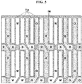
- FIG. 5 is a plan view of arrangement of pixels according to the first embodiment of the present disclosure
- FIG. 6 is a plan view of arrangement of a portion of one pixel illustrated in FIG. 5
- FIG. 7 is a diagram of arrangement of one pixel illustrated in FIG. 6
- FIG. 8 is a cross-sectional view showing an example of a region taken along A1-A2 of FIG. 7 .
- pixels according to the first embodiment may include sub-pixels each including the emissive area (e.g., R, W, B, or G) and the transparent area TRA.
- the emissive area e.g., R, W, B, or G
- the transparent area TRA e.g., R, W, B, or G
- R, W, B, G sub-pixels that emits red, white, blue, and green light
- a portion between the transparent area TRA and the emissive area e.g., R, W, B, or G
- the emissive area (e.g., R, W, B, or G) may have an " L" shape
- the transparent area TRA may have a rectangular shape different from the emissive area (e.g., R, W, B, or G).
- a vertical-direction portion may have a long rectangular shape and a horizontal-direction portion may have a polygonal shape shorter than the vertical-direction portion.
- the term horizontal-direction can be considered to be a first direction
- the term vertical-direction can be considered to be a second direction.
- the two directions being substantially perpendicular, i.e. 90 degrees to one another.
- two emissive areas that emit light with the same color may have upper and lower parts that are adjacently disposed to each other.
- the lower emissive area of the two emissive areas (e.g., R) that emit light with the same color may be formed by rotating the upper emissive area by 180°.
- two emissive areas (e.g., R) that are adjacently disposed to each other in up and down directions or right and left directions may configure a cross shape.
- a portion adjacent to two emissive areas (e.g., R or B) may configure a diagonal shape.
- Opposite edges of a vertical-direction end that is not connected to a horizontal-direction part in the emissive area may be removed rather than being formed like a straight line, but the present disclosure is not limited thereto.
- one pixel PIXEL may include a red sub-pixel having a red emissive area EMA_R and the transparent area TRA, a white sub-pixel having a white emissive area EMA_W and the transparent area TRA, a blue sub-pixel having a blue emissive area EMA_B and the transparent area TRA, and a green sub-pixel having a green emissive area EMA_G and the transparent area TRA.
- the red, white, blue, and green sub-pixels are arranged in the stated order, but the present disclosure is not limited thereto.
- the red emissive area EMA_R of the red sub-pixel may be defined by a red data line DL_R that is disposed on the left, a first reference line REF1 that is disposed on the right, and the first scan line GL1 that is disposed at a lower side.
- the transparent area TRA of the red sub-pixel may be defined by the first reference line REF1, a white data line DL_W adjacently disposed to a right side thereof, and the first scan line GL1 disposed at the lower side.
- the second driving voltage line EVSS may further disposed on the left of the red data line DL_R of the red sub-pixel.
- the second driving voltage line EVSS may correspond to a dummy voltage line that is further arranged to prevent voltage drop of the second driving voltage, and thus, may be omitted depending on the configuration of the display panel.
- the white emissive area EMA_W of the white sub-pixel may be defined by the white data line DL_W disposed on the left, a second reference line REF2 disposed on the right side, and the first scan line GL1 disposed at the lower side.
- the transparent area TRA of the white sub-pixel may be defined by the second reference line REF2, a blue data line DL_B adjacently disposed to a right side thereof, and the first scan line GL1 disposed at the lower side.
- the blue emissive area EMA_B of the blue sub-pixel may be defined by the blue data line DL_B disposed on the left, a third reference line REF3 disposed on the right, and the first scan line GL1 disposed at the lower side.
- the transparent area TRA of the blue sub-pixel may be defined by a third reference line REF3, a green data line DL_G adjacently disposed to a right side thereof, and the first scan line GL1 disposed at the lower side.
- the green emissive area EMA_G of the green sub-pixel may be defined by a green data line DL_G disposed on the left, a fourth reference line REF4 disposed on the right, and the first scan line GL1 disposed at the lower side.
- the first driving voltage line EVDD may be further disposed at a right side of the fourth reference line REF4.
- the first driving voltage line EVDD corresponds to a dummy voltage line that is further disposed to prevent voltage drop of the first driving voltage, and thus, is omitted depending on the configuration of a display panel.
- the transparent area TRA of the green sub-pixel may be defined by the first driving voltage line EVDD disposed on the left, and the first scan line GL1 disposed at the lower side.
- the transparent area TRA may also be defined by the fourth reference line REF4 and the first scan line GL1 disposed at the lower side.
- the red sub-pixel, the white sub-pixel, the blue sub-pixel, and the green sub-pixel may each include the switching transistor SW, the sensing transistor SE, the driving transistor DT, the storage capacitor CST, and an organic light emitting diode (not shown).
- an arrangement relationship of the switching transistor SW, the sensing transistor SE, the driving transistor DT, the storage capacitor CST, and the organic light emitting diode (not shown) may be the same as in the red sub-pixel, the white sub-pixel, the blue sub-pixel, and the green sub-pixel, which will be described below.
- the switching transistor SW and the sensing transistor SE are connected to the first scan line GL1, and thus, may be disposed at a lower side (a lower side of a storage capacitor) adjacent to the first scan line GL1.
- the driving transistor DT may be disposed at an upper side (an upper side of the storage capacitor) that is far away from the switching transistor SW and the sensing transistor SE.
- the storage capacitor CST may be connected to the switching transistor SW, the sensing transistor SE, the driving transistor DT, and the organic light emitting diode (not shown) and requires a wide space in order to form capacitance, and thus, may be disposed between the switching transistor SW (or a sensing transistor) and the driving transistor DT.
- each of the sub-pixels according to embodiments of the present disclosure includes the switching transistor SW, the sensing transistor SE, the driving transistor DT, the storage capacitor CST, and the organic light emitting diode (not shown), but the present disclosure is not limited thereto.
- the organic light emitting diode may cover arrangement positions of the switching transistor SW, the sensing transistor SE, the driving transistor DT, and the storage capacitor CST, which are disposed therebelow, and thus, is omitted in FIG. 7 .
- a configuration related to the organic light emitting diode will be understood based on the following description of FIG. 8 .
- the emissive area EMA_R and the transparent area TRA of the red sub-pixel may have different interlayer structures.
- the white sub-pixel, the blue sub-pixel, and the green sub-pixel may have interlayer structures shown in FIG. 8 , and thus hereinafter, the configuration of the emissive area EMA_R and the transparent area TRA will be described below based on the red sub-pixel.
- the driving transistor DT on the lower substrate 150a may be positioned in the emissive area EMA_R of the red sub-pixel.
- a lower electrode LE connected to a source electrode or a drain electrode of the driving transistor DT may be positioned on the driving transistor DT.
- the lower electrode LE may be an anode of the organic light emitting diode.
- the lower electrode LE may include a reflective layer.
- a bank layer BNK that has an opening region through which the lower electrode LE is partially exposed and defines an emissive area may be positioned on the lower electrode LE.
- An emissive layer EL may be positioned on the bank layer BNK.
- An upper electrode UE may be positioned on the emissive layer EL.
- the upper electrode UE may be a cathode of the organic light emitting diode.
- the upper electrode UE may be selected as a transparent oxide material or the like for transmitting light of the emissive layer EL therethrough.
- the aforementioned first embodiment of the present disclosure may have an effect of minimizing the width of a bank layer that occupies the largest area to embody a pixel by providing a pixel structure in which an emissive area and a transparent area are alternately disposed adjacent to each other.
- the first embodiment of the present disclosure may have an effect of enhancing transparency by forming the sub-pixel in an "L" shape and enhancing haze characteristics by dividing the transparent area for each sub-pixel.
- FIG. 9 is a first plan view of arrangement of pixels according to a second embodiment of the present disclosure
- FIG. 10 is a second plan view of arrangement of pixels according to the second embodiment of the present disclosure
- FIG. 11 is a third plan view of arrangement of pixels according to the second embodiment of the present disclosure
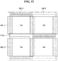
- FIG. 12 is a fourth plan view of arrangement of pixels according to the second embodiment of the present disclosure
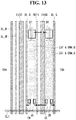
- FIG. 13 is a diagram showing arrangement of two sub-pixels shown in FIG. 10
- FIG. 14 is a diagram for further explaining another sub-pixel adjacent to the two sub-pixels shown in FIG. 10 .
- the pixels according to a first example of the second embodiment may include sub-pixels each including an emissive area (e.g., R, W, B, or G) and the transparent area TRA.
- One pixel may be defined by sub-pixels (R, W, B, and G) that emit red, white, blue, and green light, but the present disclosure is not limited thereto.
- a portion between the transparent area TRA and the emissive area (e.g., R, W, B, or G) may be defined by the black matrix BM, but the present disclosure is not limited thereto.
- the emissive area (e.g., R, W, B, or G) may have a square shape, and the transparent area TRA may have a square shape having four sides surrounded (or shared) by a plurality of emissive areas (e.g., R, W, B, or G). That is, a plurality of pixels that surround one transparent area TRA may have a shape surrounding one transparent area TRA.
- Two emissive areas that emit light with the same color (e.g., R) may be defined as one sub-pixel except that only regions are defined.
- an emissive area included in one pixel PIXEL may have a shape formed by rotating an "L" shape by 180 degrees in a counterclockwise direction (reversed "L" shape), and an emissive area that defines another pixel may be configured in an "L" shape in an opposite area. That is, at least two pixels may share one transparent area TRA while surrounding four sides of one transparent area TRA.
- one pixel PIXEL may include a red sub-pixel having the red emissive area EMA_R and the transparent area TRA, a white sub-pixel having the white emissive area EMA_W and the transparent area TRA, a blue sub-pixel having the blue emissive area EMA_B and the transparent area TRA, and a green sub-pixel having the green emissive area EMA_G and the transparent area TRA.
- the red emissive area EMA_R and the white emissive area EMA_W may be disposed in a horizontal direction and may be adjacently disposed to each other up and down, and the blue emissive area EMA_B and the green emissive area EMA_G may be disposed in a vertical direction and may be adjacently disposed to each other right and left.
- one pixel PIXEL may have a shape formed by rotating an "L" shape by 180 degrees in a counterclockwise direction when the transparent area TRA is excluded.
- the red sub-pixel and the white sub-pixel are arranged in a horizontal direction
- the blue sub-pixel and the green sub-pixel are arranged in a vertical direction, but the present disclosure is not limited thereto.
- one pixel PIXEL is formed in such a way that a circuit area DRA including circuits for driving an organic light emitting diode is positioned at a corner portion (or an edge portion) of the transparent area TRA.
- sub-pixels according to the present disclosure may be selected as a top emission type in which light is emitted in an opposite direction to a lower substrate.
- the circuit area DRA may be included in an emissive area of each sub-pixel rather than being separately defined. Accordingly, the separate circuit area DRA may not be defined.
- the pixels according to a third example of the second embodiment may be formed in such a way that a plurality of pixels that surrounds one transparent area TRA shares one transparent area TRA in the same or similar form as in the first example.
- one pixel PIXEL may have a cross shape including the red emissive area EMA_R, the white emissive area EMA_W, the blue emissive area EMA_B, and the green emissive area EMA_G.
- an emissive area included in one pixel PIXEL has a cross shape because two emissive areas that emit light with the same color are adjacently positioned on each side that surrounds the transparent area TRA.
- one emissive area may have a width corresponding to 1/2 of a horizontal or vertical side of the transparent area TRA.
- FIG. 11 illustrates an example in which the white emissive area EMA_W and the red emissive area EMA_R disposed in a horizontal direction are adjacently disposed to each other and the blue emissive area EMA_B and the green emissive area EMA_G disposed in a vertical direction are spaced apart from each other, but this is merely exemplary and the present disclosure is not limited thereto.
- the pixels according to a fourth example of the second embodiment may be formed in such a way that a plurality of pixels that surrounds one transparent area TRA shares one transparent area TRA in the same or similar form as in the second example.
- one pixel PIXEL may have a cross shape including the red emissive area EMA_R, the white emissive area EMA_W, the blue emissive area EMA_B, and the green emissive area EMA_G.
- an emissive area included in one pixel PIXEL has a cross shape because two emissive areas that emit light with the same color are adjacently positioned on each side that surrounds the transparent area TRA.
- one emissive area may have a width corresponding to a horizontal or vertical side of the transparent area TRA.
- FIG. 12 illustrates an example in which the white emissive area EMA_W and the red emissive area EMA_R disposed in a horizontal direction are adjacently disposed to each other and the blue emissive area EMA_B and the green emissive area EMA_G disposed in a vertical direction are spaced apart from each other, but this is merely exemplary and the present disclosure is not limited thereto.
- the blue emissive area EMA_B of the blue sub-pixel may be defined by the blue data line DL_B disposed on the left, the first reference line REF1 disposed on the right, and the first scan line GL1 disposed at a lower side.
- the green emissive area EMA_G of the green sub-pixel may be defined by the first driving voltage line EVDD disposed on the left, the green data line DL_G disposed on the right, and the first scan line GL1 disposed at the lower side.
- the second driving voltage line EVSS, the red data line DL_R, and the white data line DL_W may be positioned at a left side of the blue data line DL_B.
- the transparent area TRA of the blue sub-pixel may be positioned at a left side of the red data line DL_R, and the transparent area TRA of the green sub-pixel may be positioned at a right side of the green data line DL_G, but the present disclosure is not limited thereto.
- the blue sub-pixel and the green sub-pixel that are adjacent to each other may be symmetric with each other right and left based on the first reference line REF1 and the first driving voltage line EVDD to share the first reference line REF1 and the first driving voltage line EVDD. That is, the sensing transistor SE and the driving transistor DT that are respectively included in two sub-pixel may be arranged to be symmetric with each other to share the first reference line REF1 and the first driving voltage line EVDD that are disposed therebetween.
- Each of the blue sub-pixel and the green sub-pixel may include the switching transistor SW, the sensing transistor SE, the driving transistor DT, the storage capacitor CST, and the organic light emitting diode (not shown).
- an arrangement relationship of the switching transistor SW, the sensing transistor SE, the driving transistor DT, the storage capacitor CST, and the organic light emitting diode (not shown) may be the same as in the blue sub-pixel and the green sub-pixel, which will be described below.
- the switching transistor SW and the sensing transistor SE are connected to the first scan line GL1, and thus, may be disposed at a lower side (a lower side of a storage capacitor) adjacent to the first scan line GL1.
- the driving transistor DT may be disposed at an upper side (an upper side of the storage capacitor) that is far away from the switching transistor SW and the sensing transistor SE.
- the storage capacitor CST may be connected to the switching transistor SW, the sensing transistor SE, the driving transistor DT, and the organic light emitting diode (not shown) and requires a wide space in order to form capacitance, and thus, may be disposed between the switching transistor SW (or a sensing transistor) and the driving transistor DT.
- each of the sub-pixels according to embodiments of the present disclosure includes the switching transistor SW, the sensing transistor SE, the driving transistor DT, the storage capacitor CST, and the organic light emitting diode (not shown), but the present disclosure is not limited thereto.
- one pixel may have a cross shape when the transparent area TRA is excluded.
- all circuits DT, SW, SE, and CST included in one pixel may be symmetric with each other up and down or right and left.
- the blue sub-pixel and the green sub-pixel that are arranged in a vertical direction may be symmetric with each other right and left based on the first reference line REF1 and the first driving voltage line EVDD.
- the white sub-pixel and the red sub-pixel that are arranged in a horizontal direction may be symmetric with each other up and down based on the first scan line GL1.
- this is merely exemplary and at least one of circuits DT, SW, SE, and CST included in one pixel may not be symmetric with each other up and down or right and left.
- the aforementioned second embodiment of the present disclosure may have an effect of minimizing the width of a bank layer that occupies the largest area to embody a pixel having an emissive area and a transparent area.
- the second embodiment of the present disclosure may have an effect of enhancing transparency and haze characteristics by providing a pixel structure in which circuits are formed at intersections between horizontal and vertical regions and a plurality of adjacent emissive areas (sub-pixels) share one transparent area.
- the present disclosure may have an effect of enhancing transparency and haze characteristics by embodying a sub-pixel to minimize the width of a bank layer that occupies the largest area to embody a pixel having an emissive area and a transparent area and to configure the transparent area that is relatively wide compared with the emissive area.
Landscapes
- Engineering & Computer Science (AREA)
- Physics & Mathematics (AREA)
- Computer Hardware Design (AREA)
- General Physics & Mathematics (AREA)
- Theoretical Computer Science (AREA)
- Microelectronics & Electronic Packaging (AREA)
- Optics & Photonics (AREA)
- Electroluminescent Light Sources (AREA)
- Devices For Indicating Variable Information By Combining Individual Elements (AREA)
Abstract
Description
- This application claims the benefit of Korean Patent Application No.
10-2019-0160139, filed on December 04, 2019 - The present disclosure relates to a display device.
- With the development of information technologies, markets of display devices that are connection media between a user and information have expanded. Thus, display devices such as an organic light emitting display (OLED), a quantum dot display (QDD), and liquid crystal display (LCD) have been increasingly used.
- The OLED or the like includes a display panel including a plurality of sub-pixels arranged in a matrix form, a driver for outputting a driving signal for driving the display panel, and a power supply for generating power to be supplied to the display panel or the driver. The driver includes a scan driver for supplying a scan signal (or a gate signal) to the display panel, and a data driver for supplying a data signal to the display panel. The aforementioned display device displays an image by enabling a selected sub-pixel to transmit light therethrough or to directly emit light when a driving signal, e.g., a scan signal and a data signal is supplied to sub-pixels formed on a display panel.
- Some of the aforementioned display devices, for example, the OLED has the excellent response speed, viewing angle, and contrast ratio, and is easily thinned. The OLED includes a display panel configured to have a separate transparent area as well as a light emissive area, and thus, has been studied as a next-generation display device in various fields.
- The present disclosure provides a display device including a lower substrate, and a pixel including sub-pixels having one transparent area defined to transmit light on the lower substrate and a plurality of emissive areas disposed around the one transparent area and defined to emit light with at least three different colors.
- In another aspect, the present disclosure provides a display device including a lower substrate, and a pixel including sub-pixels having one transparent area defined to transmit light on the lower substrate and one emissive area defined to emit light, wherein the one emissive area has an "L" shape.
- In yet another aspect, the present disclosure provides a display device including a lower substrate, and a pixel including sub-pixels having one transparent area defined to transmit light on the lower substrate and a plurality of emissive areas disposed on four sides of the one transparent area and defined to emit light with at least three different colors.
- The accompanying drawings, which are included to provide a further understanding of the present disclosure and are incorporated in and constitute a part of this application, illustrate embodiment(s) of the present disclosure and together with the description serve to explain the principle of the present disclosure. In the drawings:
-
FIG. 1 is a schematic block diagram showing an organic light emitting display (OLED),FIG. 2 is a schematic diagram showing a configuration of a sub-pixel shown inFIG. 1 ,FIG. 3 is a diagram showing an example of a detailed circuit configuration of a sub-pixel shown inFIG. 1 , andFIG. 4 is a cross-sectional view for explaining a function of a display panel shown inFIG. 1 ; -
FIG. 5 is a plan view of arrangement of pixels according to the first embodiment of the present disclosure,FIG. 6 is a plan view of arrangement of a portion of one pixel illustrated inFIG. 5 ,FIG. 7 is a diagram of arrangement of one pixel illustrated inFIG. 6 , andFIG. 8 is a cross-sectional view showing an example of a region taken along A1-A2 ofFIG. 7 ; and -
FIG. 9 is a first plan view of arrangement of pixels according to a second embodiment of the present disclosure,FIG. 10 is a second plan view of arrangement of pixels according to the second embodiment of the present disclosure,FIG. 11 is a third plan view of arrangement of pixels according to the second embodiment of the present disclosure,FIG. 12 is a fourth plan view of arrangement of pixels according to the second embodiment of the present disclosure,FIG. 13 is a diagram showing arrangement of two sub-pixels shown inFIG. 10 , andFIG. 14 is a diagram for further explaining another sub-pixel adjacent to the two sub-pixels shown inFIG. 10 . - Reference will now be made to detailed embodiments of the present disclosure, examples of which are illustrated in the accompanying drawings.
- With the development of information technologies, markets of display devices that are connection media between a user and information have expanded. Thus, display devices such as an organic light emitting display (OLED), a quantum dot display (QDD), and liquid crystal display (LCD) have been increasingly used.
- Hereinafter, an OLED including an organic light emitting diode will be described with regard to exemplary embodiments of the present disclosure but the present disclosure may also be applied to other display devices including an inorganic light emitting display.
-
FIG. 1 is a schematic block diagram showing an OLED,FIG. 2 is a schematic diagram showing a configuration of a sub-pixel shown inFIG. 1 ,FIG. 3 is a diagram showing an example of a detailed circuit configuration of a sub-pixel shown inFIG. 1 , andFIG. 4 is a cross-sectional view for explaining a function of a display panel shown inFIG. 1 . - As shown in
FIG. 1 , the OLED may include an image supply 110, a timing controller 120, ascan driver 130, adata driver 140, adisplay panel 150, and apower supply 180. - The image supply 110 may output various driving signals with an image data signal supplied from the outside or an image data signal stored in an internal memory. The image supply 110 may supply a data signal and various driving signals to the timing controller 120.
- The timing controller 120 may output a gate timing control signal GDC for controlling operation timing of the
scan driver 130, a data timing control signal DDC for controlling operation timing of thedata driver 140, and various synchronization signals (vertical synchronization signal Vsync and horizontal synchronization signal Hsync). The timing controller 120 may supply the data signal DATA supplied from the image supply 110 with the data timing control signal DDC to thedata driver 140. - The
scan driver 130 may output the scan signal (or a gate signal) in response to the gate timing control signal GDC or the like, which is supplied from the timing controller 120. Thescan driver 130 may supply the scan signal to sub-pixels included in thedisplay panel 150 through scan lines GL1 to GLm. Thescan driver 130 may be formed in the form of an integrated circuit (IC) or may be directly formed on thedisplay panel 150 in a gate in panel method. - The
data driver 140 may sample and latch a data signal DATA in response to the data timing control signal DDC or the like supplied from the timing controller 120, may convert the data signal DATA into a data voltage in the form of an analog signal corresponding to a gamma reference voltage, and may output the data voltage. Thedata driver 140 may supply a data voltage to sub-pixels included in thedisplay panel 150 through data lines DL1 to DLn. Thedata driver 140 may be formed in the formed of an integrated circuit (IC) and may be installed on thedisplay panel 150 or may be installed on a printed circuit board, but the present disclosure is not limited thereto. - The
power supply 180 may generate and output a first driving voltage EVDD with a high potential and a second driving voltage EVSS with a low potential based on an external input voltage supplied from the outside. Thepower supply 180 may generate and output a voltage (e.g., a scan high voltage or a scan low voltage) required to drive thescan driver 130 or a voltage (a drain voltage or a half drain voltage) required to drive thedata driver 140 as well as the first and second driving voltages EVDD and EVSS. - The
display panel 150 may display an image in response to the driving signal including a scan signal and the data voltage output from the driver including thescan driver 130 and thedata driver 140, and the first and second driving voltages EVDD and EVSS output from thepower supply 180. The sub-pixels of thedisplay panel 150 may directly emit light. - As shown in
FIG. 2 , one sub-pixel SP may be defined by a first data line DL1, a first scan line GL1, the first driving voltage line EVDD, and the second driving voltage line EVSS. In addition, one sub-pixel SP may include a switching transistor SW, and a pixel circuit PC including a driving transistor, a storage capacitor, an organic light emitting diode, or the like. - The sub-pixel SP used in the OLED may directly emit light and may have a complicated circuit configuration compared with a liquid crystal display. In addition, a compensation circuit for compensating for degradation of a driving transistor for supplying driving current to an organic light emitting diode as well as the organic light emitting diode for emitting light may be complicated and diversified. Thus, it may be noted that the pixel circuit PC included in the sub-pixel SP is illustrated in the form of a block. However, according to the present disclosure, the sub-pixel SP may be embodied based on at least the configuration shown in
FIG. 3 . - As shown in
FIG. 3 , one sub-pixel SP may include the switching transistor SW, a driving transistor DT, a sensing transistor SE, a storage capacitor CST, and an organic light emitting diode OLED. - The switching transistor SW may have a gate electrode connected to the first scan line GL1, a first electrode connected to the first data line DL1, and a second electrode connected to a gate electrode of the driving transistor DT and one end of the storage capacitor CST. The switching transistor SW may apply a data voltage transferred through the first data line DL1 to one end of the storage capacitor CST.
- The driving transistor DT may have the gate electrode connected to the second electrode of the switching transistor SW and one end of the storage capacitor CST, a first electrode connected to the first driving voltage line EVDD, and a second electrode connected to the other end of the storage capacitor CST and an anode of the organic light emitting diode OLED. The driving transistor DT may generate driving current based on a data voltage stored in the storage capacitor CST.
- The sensing transistor SE may have a gate electrode connected to the first scan line GL1, a first electrode connected to the second electrode of the driving transistor DT and an anode of the organic light emitting diode OLED, and a second electrode connected to a referenced line REF. The sensing transistor SE may sense the characteristics (threshold voltage or current mobility) of the driving transistor DT or the characteristics (threshold voltage) of the organic light emitting diode OLED and may then transfer the sensed characteristics to an external circuit.
- The storage capacitor CST may have one end connected to the second electrode of the switching transistor SW and the gate electrode of the driving transistor DT, and the other end connected to the second electrode of the driving transistor DT, the first electrode of the sensing transistor SE, and the anode of the organic light emitting diode OLED. The storage capacitor CST may store a data voltage and may transfer the data voltage to the gate electrode of the driving transistor DT.
- The organic light emitting diode OLED may have the anode connected to the second electrode of the driving transistor DT, the first electrode of the sensing transistor SE, and the other end of the storage capacitor CST, and a cathode connected to the second driving voltage line EVSS. The organic light emitting diode OLED may emit light in response to the driving current generated by the driving transistor DT. Hereinafter, an example in which a display panel is embodied based on the sub-pixel shown in
FIG. 3 will be described with regard to the present disclosure. - As shown in
FIG. 4 , thedisplay panel 150 according to a first embodiment of the present disclosure may include adisplay part 160 positioned between alower substrate 150a and anupper substrate 150b. Thedisplay part 160 may be embodied based on the sub-pixel described with reference toFIG. 3 . - The
lower substrate 150a and theupper substrate 150b may be selected as the same material or different materials. For example, thelower substrate 150a may be selected as a single material such as resin having flexibility or glass having rigidity, and theupper substrate 150b may be selected as a composite material such as organic/inorganic material, but the present disclosure is not limited thereto. - The
display part 160 may have an emissive area EMA that directly emits light and a transparent area TRA that does not emit light but transmits external light therethrough. In order to embody thedisplay panel 150 as described above, an example in which one sub-pixel includes the emissive area EMA and the transparent area TRA is described, but the present disclosure is not limited thereto. - As described above, the OLED has the excellent response speed, viewing angle, and contrast ratio, and is easily thinned. The OLED includes a display panel configured to have a separate transparent area as well as a light emissive area, and thus, has been studied as a next-generation display device in various fields. The present disclosure provides the following configuration in order to enhance the transparency and haze of an OLED having an emissive area and a transparent area.
-
FIG. 5 is a plan view of arrangement of pixels according to the first embodiment of the present disclosure,FIG. 6 is a plan view of arrangement of a portion of one pixel illustrated inFIG. 5 ,FIG. 7 is a diagram of arrangement of one pixel illustrated inFIG. 6 , andFIG. 8 is a cross-sectional view showing an example of a region taken along A1-A2 ofFIG. 7 . - As shown in
FIG. 5 , pixels according to the first embodiment may include sub-pixels each including the emissive area (e.g., R, W, B, or G) and the transparent area TRA. An example in which one pixel is defined by sub-pixels (R, W, B, G) that emits red, white, blue, and green light is described, but the present disclosure is not limited thereto. A portion between the transparent area TRA and the emissive area (e.g., R, W, B, or G) may be defined by a black matrix BM, but the present disclosure is not limited thereto. - The emissive area (e.g., R, W, B, or G) may have an "L" shape, and the transparent area TRA may have a rectangular shape different from the emissive area (e.g., R, W, B, or G). In the emissive area (e.g., R, W, B, or G), a vertical-direction portion may have a long rectangular shape and a horizontal-direction portion may have a polygonal shape shorter than the vertical-direction portion. The term horizontal-direction can be considered to be a first direction, and the term vertical-direction can be considered to be a second direction. The two directions being substantially perpendicular, i.e. 90 degrees to one another.
- In the emissive area (e.g., R, W, B, or G), two emissive areas (e.g., R or B) that emit light with the same color may have upper and lower parts that are adjacently disposed to each other. In this case, the lower emissive area of the two emissive areas (e.g., R) that emit light with the same color may be formed by rotating the upper emissive area by 180°. As a result, two emissive areas (e.g., R) that are adjacently disposed to each other in up and down directions or right and left directions may configure a cross shape. A portion adjacent to two emissive areas (e.g., R or B) may configure a diagonal shape.
- Opposite edges of a vertical-direction end that is not connected to a horizontal-direction part in the emissive area (e.g., R, W, B, or G) may be removed rather than being formed like a straight line, but the present disclosure is not limited thereto.
- As shown in
FIG. 6 , one pixel PIXEL may include a red sub-pixel having a red emissive area EMA_R and the transparent area TRA, a white sub-pixel having a white emissive area EMA_W and the transparent area TRA, a blue sub-pixel having a blue emissive area EMA_B and the transparent area TRA, and a green sub-pixel having a green emissive area EMA_G and the transparent area TRA. In addition, viewed from the above, the red, white, blue, and green sub-pixels are arranged in the stated order, but the present disclosure is not limited thereto. - As shown in
FIG. 7 , the red emissive area EMA_R of the red sub-pixel may be defined by a red data line DL_R that is disposed on the left, a first reference line REF1 that is disposed on the right, and the first scan line GL1 that is disposed at a lower side. The transparent area TRA of the red sub-pixel may be defined by the first reference line REF1, a white data line DL_W adjacently disposed to a right side thereof, and the first scan line GL1 disposed at the lower side. The second driving voltage line EVSS may further disposed on the left of the red data line DL_R of the red sub-pixel. The second driving voltage line EVSS may correspond to a dummy voltage line that is further arranged to prevent voltage drop of the second driving voltage, and thus, may be omitted depending on the configuration of the display panel. - The white emissive area EMA_W of the white sub-pixel may be defined by the white data line DL_W disposed on the left, a second reference line REF2 disposed on the right side, and the first scan line GL1 disposed at the lower side. The transparent area TRA of the white sub-pixel may be defined by the second reference line REF2, a blue data line DL_B adjacently disposed to a right side thereof, and the first scan line GL1 disposed at the lower side.
- The blue emissive area EMA_B of the blue sub-pixel may be defined by the blue data line DL_B disposed on the left, a third reference line REF3 disposed on the right, and the first scan line GL1 disposed at the lower side. The transparent area TRA of the blue sub-pixel may be defined by a third reference line REF3, a green data line DL_G adjacently disposed to a right side thereof, and the first scan line GL1 disposed at the lower side.
- The green emissive area EMA_G of the green sub-pixel may be defined by a green data line DL_G disposed on the left, a fourth reference line REF4 disposed on the right, and the first scan line GL1 disposed at the lower side. The first driving voltage line EVDD may be further disposed at a right side of the fourth reference line REF4. The first driving voltage line EVDD corresponds to a dummy voltage line that is further disposed to prevent voltage drop of the first driving voltage, and thus, is omitted depending on the configuration of a display panel. Thus, the transparent area TRA of the green sub-pixel may be defined by the first driving voltage line EVDD disposed on the left, and the first scan line GL1 disposed at the lower side. The transparent area TRA may also be defined by the fourth reference line REF4 and the first scan line GL1 disposed at the lower side.
- As described above with reference to
FIG. 3 , the red sub-pixel, the white sub-pixel, the blue sub-pixel, and the green sub-pixel may each include the switching transistor SW, the sensing transistor SE, the driving transistor DT, the storage capacitor CST, and an organic light emitting diode (not shown). In addition, based on the first scan line GL1, an arrangement relationship of the switching transistor SW, the sensing transistor SE, the driving transistor DT, the storage capacitor CST, and the organic light emitting diode (not shown) may be the same as in the red sub-pixel, the white sub-pixel, the blue sub-pixel, and the green sub-pixel, which will be described below. - The switching transistor SW and the sensing transistor SE are connected to the first scan line GL1, and thus, may be disposed at a lower side (a lower side of a storage capacitor) adjacent to the first scan line GL1. The driving transistor DT may be disposed at an upper side (an upper side of the storage capacitor) that is far away from the switching transistor SW and the sensing transistor SE.
- The storage capacitor CST may be connected to the switching transistor SW, the sensing transistor SE, the driving transistor DT, and the organic light emitting diode (not shown) and requires a wide space in order to form capacitance, and thus, may be disposed between the switching transistor SW (or a sensing transistor) and the driving transistor DT. However, although each of the sub-pixels according to embodiments of the present disclosure includes the switching transistor SW, the sensing transistor SE, the driving transistor DT, the storage capacitor CST, and the organic light emitting diode (not shown), but the present disclosure is not limited thereto.
- The organic light emitting diode (not shown) may cover arrangement positions of the switching transistor SW, the sensing transistor SE, the driving transistor DT, and the storage capacitor CST, which are disposed therebelow, and thus, is omitted in
FIG. 7 . However, a configuration related to the organic light emitting diode (not shown) will be understood based on the following description ofFIG. 8 . - As shown in
FIG. 8 , the emissive area EMA_R and the transparent area TRA of the red sub-pixel may have different interlayer structures. The white sub-pixel, the blue sub-pixel, and the green sub-pixel may have interlayer structures shown inFIG. 8 , and thus hereinafter, the configuration of the emissive area EMA_R and the transparent area TRA will be described below based on the red sub-pixel. - The driving transistor DT on the
lower substrate 150a may be positioned in the emissive area EMA_R of the red sub-pixel. A lower electrode LE connected to a source electrode or a drain electrode of the driving transistor DT may be positioned on the driving transistor DT. The lower electrode LE may be an anode of the organic light emitting diode. The lower electrode LE may include a reflective layer. - A bank layer BNK that has an opening region through which the lower electrode LE is partially exposed and defines an emissive area may be positioned on the lower electrode LE. An emissive layer EL may be positioned on the bank layer BNK. An upper electrode UE may be positioned on the emissive layer EL. The upper electrode UE may be a cathode of the organic light emitting diode. The upper electrode UE may be selected as a transparent oxide material or the like for transmitting light of the emissive layer EL therethrough.
- An example in which only the
lower substrate 150a is present in the transparent area TRA of the red sub-pixel without another structure layer is illustrated. However, an insulating layer or the like that is commonly formed on an entire part of thelower substrate 150a irrespective of transmission of light may also be positioned in the transparent area TRA of the red sub-pixel. - The aforementioned first embodiment of the present disclosure may have an effect of minimizing the width of a bank layer that occupies the largest area to embody a pixel by providing a pixel structure in which an emissive area and a transparent area are alternately disposed adjacent to each other. In addition, the first embodiment of the present disclosure may have an effect of enhancing transparency by forming the sub-pixel in an "L" shape and enhancing haze characteristics by dividing the transparent area for each sub-pixel.
-
FIG. 9 is a first plan view of arrangement of pixels according to a second embodiment of the present disclosure,FIG. 10 is a second plan view of arrangement of pixels according to the second embodiment of the present disclosure,FIG. 11 is a third plan view of arrangement of pixels according to the second embodiment of the present disclosure,FIG. 12 is a fourth plan view of arrangement of pixels according to the second embodiment of the present disclosure,FIG. 13 is a diagram showing arrangement of two sub-pixels shown inFIG. 10 , andFIG. 14 is a diagram for further explaining another sub-pixel adjacent to the two sub-pixels shown inFIG. 10 . - As shown in
FIG. 9 , the pixels according to a first example of the second embodiment may include sub-pixels each including an emissive area (e.g., R, W, B, or G) and the transparent area TRA. One pixel may be defined by sub-pixels (R, W, B, and G) that emit red, white, blue, and green light, but the present disclosure is not limited thereto. A portion between the transparent area TRA and the emissive area (e.g., R, W, B, or G) may be defined by the black matrix BM, but the present disclosure is not limited thereto. - The emissive area (e.g., R, W, B, or G) may have a square shape, and the transparent area TRA may have a square shape having four sides surrounded (or shared) by a plurality of emissive areas (e.g., R, W, B, or G). That is, a plurality of pixels that surround one transparent area TRA may have a shape surrounding one transparent area TRA. Two emissive areas that emit light with the same color (e.g., R) may be defined as one sub-pixel except that only regions are defined.
- In the emissive area (e.g., R, W, B, or G), two emissive areas (e.g., R or W) that emit light with the same color may be adjacently disposed to each other right and left in a horizontal direction, and two emissive areas (e.g., B or G) that emit light with the same color may be adjacently disposed to each other up and down in a vertical direction. As a result, an emissive area included in one pixel PIXEL may have a shape formed by rotating an "L" shape by 180 degrees in a counterclockwise direction (reversed "L" shape), and an emissive area that defines another pixel may be configured in an "L" shape in an opposite area. That is, at least two pixels may share one transparent area TRA while surrounding four sides of one transparent area TRA.
- As shown in
FIG. 10 , the pixels according to a second example of the second embodiment may be formed in such a way that a plurality of pixels that surrounds one transparent area TRA shares one transparent area TRA in the same or similar form as in the first example. To this end, one pixel PIXEL may include a red sub-pixel having the red emissive area EMA_R and the transparent area TRA, a white sub-pixel having the white emissive area EMA_W and the transparent area TRA, a blue sub-pixel having the blue emissive area EMA_B and the transparent area TRA, and a green sub-pixel having the green emissive area EMA_G and the transparent area TRA. - The red emissive area EMA_R and the white emissive area EMA_W may be disposed in a horizontal direction and may be adjacently disposed to each other up and down, and the blue emissive area EMA_B and the green emissive area EMA_G may be disposed in a vertical direction and may be adjacently disposed to each other right and left. As a result, one pixel PIXEL may have a shape formed by rotating an "L" shape by 180 degrees in a counterclockwise direction when the transparent area TRA is excluded.
- Viewed from a portion of pixels having a shape formed by rotating an "L" shape by 180 degrees in a counterclockwise direction, the red sub-pixel and the white sub-pixel are arranged in a horizontal direction, and the blue sub-pixel and the green sub-pixel are arranged in a vertical direction, but the present disclosure is not limited thereto.
- For example, one pixel PIXEL is formed in such a way that a circuit area DRA including circuits for driving an organic light emitting diode is positioned at a corner portion (or an edge portion) of the transparent area TRA. However, sub-pixels according to the present disclosure may be selected as a top emission type in which light is emitted in an opposite direction to a lower substrate. Thus, the circuit area DRA may be included in an emissive area of each sub-pixel rather than being separately defined. Accordingly, the separate circuit area DRA may not be defined.
- As shown in
FIG. 11 , the pixels according to a third example of the second embodiment may be formed in such a way that a plurality of pixels that surrounds one transparent area TRA shares one transparent area TRA in the same or similar form as in the first example. In this case, when the transparent area TRA is excluded, one pixel PIXEL may have a cross shape including the red emissive area EMA_R, the white emissive area EMA_W, the blue emissive area EMA_B, and the green emissive area EMA_G. - As such, an emissive area included in one pixel PIXEL has a cross shape because two emissive areas that emit light with the same color are adjacently positioned on each side that surrounds the transparent area TRA. Here, one emissive area may have a width corresponding to 1/2 of a horizontal or vertical side of the transparent area TRA.
-
FIG. 11 illustrates an example in which the white emissive area EMA_W and the red emissive area EMA_R disposed in a horizontal direction are adjacently disposed to each other and the blue emissive area EMA_B and the green emissive area EMA_G disposed in a vertical direction are spaced apart from each other, but this is merely exemplary and the present disclosure is not limited thereto. - As shown in
FIG. 12 , the pixels according to a fourth example of the second embodiment may be formed in such a way that a plurality of pixels that surrounds one transparent area TRA shares one transparent area TRA in the same or similar form as in the second example. In this case, when the transparent area TRA is excluded, one pixel PIXEL may have a cross shape including the red emissive area EMA_R, the white emissive area EMA_W, the blue emissive area EMA_B, and the green emissive area EMA_G. - As such, an emissive area included in one pixel PIXEL has a cross shape because two emissive areas that emit light with the same color are adjacently positioned on each side that surrounds the transparent area TRA. Here, one emissive area may have a width corresponding to a horizontal or vertical side of the transparent area TRA.
-
FIG. 12 illustrates an example in which the white emissive area EMA_W and the red emissive area EMA_R disposed in a horizontal direction are adjacently disposed to each other and the blue emissive area EMA_B and the green emissive area EMA_G disposed in a vertical direction are spaced apart from each other, but this is merely exemplary and the present disclosure is not limited thereto. - As shown in
FIG. 13 , the blue emissive area EMA_B of the blue sub-pixel may be defined by the blue data line DL_B disposed on the left, the first reference line REF1 disposed on the right, and the first scan line GL1 disposed at a lower side. The green emissive area EMA_G of the green sub-pixel may be defined by the first driving voltage line EVDD disposed on the left, the green data line DL_G disposed on the right, and the first scan line GL1 disposed at the lower side. - The second driving voltage line EVSS, the red data line DL_R, and the white data line DL_W may be positioned at a left side of the blue data line DL_B. The transparent area TRA of the blue sub-pixel may be positioned at a left side of the red data line DL_R, and the transparent area TRA of the green sub-pixel may be positioned at a right side of the green data line DL_G, but the present disclosure is not limited thereto.
- The blue sub-pixel and the green sub-pixel that are adjacent to each other may be symmetric with each other right and left based on the first reference line REF1 and the first driving voltage line EVDD to share the first reference line REF1 and the first driving voltage line EVDD. That is, the sensing transistor SE and the driving transistor DT that are respectively included in two sub-pixel may be arranged to be symmetric with each other to share the first reference line REF1 and the first driving voltage line EVDD that are disposed therebetween.
- Each of the blue sub-pixel and the green sub-pixel may include the switching transistor SW, the sensing transistor SE, the driving transistor DT, the storage capacitor CST, and the organic light emitting diode (not shown). In addition, as described above with reference to
FIG. 7 , based on the first scan line GL1, an arrangement relationship of the switching transistor SW, the sensing transistor SE, the driving transistor DT, the storage capacitor CST, and the organic light emitting diode (not shown) may be the same as in the blue sub-pixel and the green sub-pixel, which will be described below. - The switching transistor SW and the sensing transistor SE are connected to the first scan line GL1, and thus, may be disposed at a lower side (a lower side of a storage capacitor) adjacent to the first scan line GL1. The driving transistor DT may be disposed at an upper side (an upper side of the storage capacitor) that is far away from the switching transistor SW and the sensing transistor SE.
- The storage capacitor CST may be connected to the switching transistor SW, the sensing transistor SE, the driving transistor DT, and the organic light emitting diode (not shown) and requires a wide space in order to form capacitance, and thus, may be disposed between the switching transistor SW (or a sensing transistor) and the driving transistor DT. However, although each of the sub-pixels according to embodiments of the present disclosure includes the switching transistor SW, the sensing transistor SE, the driving transistor DT, the storage capacitor CST, and the organic light emitting diode (not shown), but the present disclosure is not limited thereto.
- As shown in
FIG. 14 , one pixel may have a cross shape when the transparent area TRA is excluded. When one pixel has a cross shape, all circuits DT, SW, SE, and CST included in one pixel may be symmetric with each other up and down or right and left. - In addition to the above description, the blue sub-pixel and the green sub-pixel that are arranged in a vertical direction may be symmetric with each other right and left based on the first reference line REF1 and the first driving voltage line EVDD. The white sub-pixel and the red sub-pixel that are arranged in a horizontal direction may be symmetric with each other up and down based on the first scan line GL1. However, this is merely exemplary and at least one of circuits DT, SW, SE, and CST included in one pixel may not be symmetric with each other up and down or right and left.
- The aforementioned second embodiment of the present disclosure may have an effect of minimizing the width of a bank layer that occupies the largest area to embody a pixel having an emissive area and a transparent area. In addition, the second embodiment of the present disclosure may have an effect of enhancing transparency and haze characteristics by providing a pixel structure in which circuits are formed at intersections between horizontal and vertical regions and a plurality of adjacent emissive areas (sub-pixels) share one transparent area.
- According to the aforementioned first and second embodiments of the present disclosure, as seen from Table 1 below, transparency defined by a transparent area is enhanced while maintaining an aperture ratio defined by an emissive area at a level of 30% which is the same or similar as in the conventional case. In Table 1 below, a conventional structure is formed in such a way that all emissive areas of red, green, blue, and white sub-pixels are adjacently and closed to each other and a region adjacent thereto is used as a transparent area.
[Table 1] Division Conventional structure First Embodiment Second Embodiment Transparency 40% 50.7% 52.4% (+10.7%) (+12.4%) Aperture ratio 30% 30% 30% - The present disclosure may have an effect of enhancing transparency and haze characteristics by embodying a sub-pixel to minimize the width of a bank layer that occupies the largest area to embody a pixel having an emissive area and a transparent area and to configure the transparent area that is relatively wide compared with the emissive area.
- Also disclosed are the following numbered clauses:
- 1. A display device comprising:
- a lower substrate; and
- a pixel including sub-pixels having one transparent area defined to transmit light on the lower substrate and a plurality of emissive areas disposed around the one transparent area and defined to emit light with at least three different colors.
- 2. The display device of clause 1, wherein the plurality of emissive areas are arranged to surround the one transparent area.
- 3. The display device of any preceding clause, wherein the pixel includes a red sub-pixel having a red emissive area, a white sub-pixel having a white emissive area, a blue sub-pixel having a blue emissive area, and a green sub-pixel having a green emissive area; and
wherein the red sub-pixel, the white sub-pixel, the blue sub-pixel, and the green sub-pixel have an "L" shape or a shape formed by rotating the "L" shape, which surrounds a first surface and a second surface of the one transparent area. - 4. The display device of any preceding clause, wherein the one transparent area has a square shape having four sides surrounded by emissive areas included at least two pixels.
- 5. The display device of any preceding clause, wherein one of the plurality of emissive areas has a width corresponding to 1/2 of a horizontal or vertical side of the one transparent area.
- 6. The display device of any preceding clause, wherein one of the plurality of emissive areas has a width corresponding to a horizontal or vertical side of the one transparent area.
- 7. The display device of clause 6, wherein the one emissive area is divided in a horizontal or vertical direction.
- 8. A display device comprising:
- a lower substrate; and
- a pixel including sub-pixels each having one transparent area defined to transmit light on the lower substrate and one emissive area defined to emit light,
- wherein the one emissive area has an "L" shape.
- 9. The display device of clause 8, wherein an emissive area having a cross shape is disposed on the lower substrate and is configured by two emissive area having the "L" shape, and that are adjacent to each other up and down or right and left and emit light with the same color.
- 10. The display device of clause 9, wherein a portion adjacent to the two emissive areas has a diagonal shape.
- 11. A display device comprising:
- a lower substrate; and
- a pixel including sub-pixels having one transparent area defined to transmit light on the lower substrate and a plurality of emissive areas disposed on four sides of the one transparent area and defined to emit light with at least three different colors.
- 12. The display device of clause 11, wherein at least two emissive areas of the plurality of emissive areas are arranged on one side of the one transparent area.
- 13. The display device of
clause 12, wherein each sub-pixel on the lower substrate includes a circuit area including circuits for driving an organic light emitting diode, the circuit area disposed at a corner portion of the one transparent area.
Claims (7)
- A display device comprising:a lower substrate; anda pixel including sub-pixels, the pixel having a transparent area configured to transmit light therethrough and onto the lower substrate, and a plurality of emissive areas disposed around the transparent area and configured to emit light with at least three different colors.
- The display device of claim 1, wherein the plurality of emissive areas are arranged to surround the transparent area.
- The display device of any preceding claim, wherein the pixel includes a red sub-pixel having a red emissive area, a white sub-pixel having a white emissive area, a blue sub-pixel having a blue emissive area, and a green sub-pixel having a green emissive area; and
wherein the red sub-pixel, the white sub-pixel, the blue sub-pixel, and the green sub-pixel have an "L" shape or a shape formed by rotating the "L" shape, which surrounds a first surface and a second surface of the transparent area. - The display device of any preceding claim, wherein the transparent area has a square shape having four sides surrounded by emissive areas included at least two pixels.
- The display device of any preceding claim, wherein one of the plurality of emissive areas has a width corresponding to 1/2 of a side of a first direction or 1/2 of a side of a second direction of the transparent area, the first and second directions being 90 degrees to one another.
- The display device of any preceding claim, wherein one of the plurality of emissive areas has a width corresponding to a side of a first direction or a side of a second direction of the transparent area, the first and second directions being 90 degrees to one another.
- The display device of claim 6, wherein the one emissive area is divided in a first direction or a second direction, the first and second directions being 90 degrees to one another.
Applications Claiming Priority (1)
| Application Number | Priority Date | Filing Date | Title |
|---|---|---|---|
| KR1020190160139A KR20210070091A (en) | 2019-12-04 | 2019-12-04 | Display Device |
Publications (1)
| Publication Number | Publication Date |
|---|---|
| EP3832634A1 true EP3832634A1 (en) | 2021-06-09 |
Family
ID=73646163
Family Applications (1)
| Application Number | Title | Priority Date | Filing Date |
|---|---|---|---|
| EP20210614.2A Pending EP3832634A1 (en) | 2019-12-04 | 2020-11-30 | Display device |
Country Status (4)
| Country | Link |
|---|---|
| US (1) | US11751458B2 (en) |
| EP (1) | EP3832634A1 (en) |
| KR (1) | KR20210070091A (en) |
| CN (1) | CN112909045B (en) |
Families Citing this family (7)
| Publication number | Priority date | Publication date | Assignee | Title |
|---|---|---|---|---|
| CN114097102B (en) | 2019-06-26 | 2023-11-03 | Oti照明公司 | Optoelectronic device comprising a light transmissive region having light diffraction features |
| US11832473B2 (en) | 2019-06-26 | 2023-11-28 | Oti Lumionics Inc. | Optoelectronic device including light transmissive regions, with light diffraction characteristics |
| CN114342068A (en) | 2019-08-09 | 2022-04-12 | Oti照明公司 | Optoelectronic device comprising auxiliary electrodes and partitions |
| WO2022123431A1 (en) | 2020-12-07 | 2022-06-16 | Oti Lumionics Inc. | Patterning a conductive deposited layer using a nucleation inhibiting coating and an underlying metallic coating |
| CN113178140B (en) * | 2021-04-27 | 2023-07-14 | 上海天马微电子有限公司 | Display panel and display device |
| CN115101564A (en) | 2022-06-27 | 2022-09-23 | 武汉天马微电子有限公司 | Display panel and display device |
| US20260006965A1 (en) * | 2024-06-26 | 2026-01-01 | Samsung Display Co., Ltd. | Display device and electronic device including the same |
Citations (3)
| Publication number | Priority date | Publication date | Assignee | Title |
|---|---|---|---|---|
| EP2866261A1 (en) * | 2013-10-18 | 2015-04-29 | Samsung Display Co., Ltd. | Organic light emitting display device |
| US20160163770A1 (en) * | 2014-12-05 | 2016-06-09 | Lg Display Co., Ltd. | Transparent organic light emitting display device and method of manufacturing the same |
| US20170053971A1 (en) * | 2015-08-21 | 2017-02-23 | Japan Display Inc. | Display device |
Family Cites Families (16)
| Publication number | Priority date | Publication date | Assignee | Title |
|---|---|---|---|---|
| KR100567305B1 (en) * | 2003-02-20 | 2006-04-04 | 산요덴키가부시키가이샤 | Color electro luminescence display device |
| KR102045242B1 (en) * | 2013-06-21 | 2019-11-15 | 엘지디스플레이 주식회사 | Display apparatus |
| KR102274586B1 (en) | 2013-10-31 | 2021-07-07 | 엘지디스플레이 주식회사 | Transparent organic light emitting display device and method of decreasing reflection of light at the same |
| JP6223210B2 (en) * | 2014-01-30 | 2017-11-01 | 株式会社ジャパンディスプレイ | Display device |
| KR102184784B1 (en) * | 2014-06-30 | 2020-11-30 | 엘지디스플레이 주식회사 | Transparent organic light emitting display device |
| KR102291485B1 (en) | 2014-10-21 | 2021-08-20 | 삼성디스플레이 주식회사 | Transparent organic light emitting display device and the manufacturing method thereof |
| JP2016201216A (en) * | 2015-04-08 | 2016-12-01 | 株式会社ジャパンディスプレイ | Display device and manufacturing method of display device |
| KR102453420B1 (en) | 2015-04-30 | 2022-10-13 | 삼성디스플레이 주식회사 | Transparent organic light emitting display device and method of manufacturing organic light emitting display device |
| CN104795434B (en) * | 2015-05-12 | 2019-01-29 | 京东方科技集团股份有限公司 | OLED pixel unit, transparent display device and manufacturing method, display device |
| US9761171B2 (en) * | 2015-08-20 | 2017-09-12 | Chunghwa Picture Tubes, Ltd. | Pixel array of active matrix organic lighting emitting diode display, method of driving the same, and method of driving dual pixel of active matrix organic lighting emitting diode display |
| KR102500273B1 (en) * | 2015-10-19 | 2023-02-16 | 삼성디스플레이 주식회사 | Ddisplay apparatus |
| KR20170073018A (en) | 2015-12-17 | 2017-06-28 | 삼성디스플레이 주식회사 | Transparent display panel and transparent display device including the same |
| KR102636147B1 (en) | 2015-12-31 | 2024-02-08 | 엘지디스플레이 주식회사 | Transparent display device |
| KR102446875B1 (en) * | 2016-01-22 | 2022-09-26 | 삼성디스플레이 주식회사 | display device |
| CN108962021A (en) * | 2017-05-23 | 2018-12-07 | 群创光电股份有限公司 | Display panel |
| CN111435202B (en) * | 2019-01-11 | 2025-05-30 | 成都京东方光电科技有限公司 | Display substrate, display panel and display device |
-
2019
- 2019-12-04 KR KR1020190160139A patent/KR20210070091A/en active Pending
-
2020
- 2020-11-26 CN CN202011345629.1A patent/CN112909045B/en active Active
- 2020-11-30 EP EP20210614.2A patent/EP3832634A1/en active Pending
- 2020-12-01 US US17/108,856 patent/US11751458B2/en active Active
Patent Citations (3)
| Publication number | Priority date | Publication date | Assignee | Title |
|---|---|---|---|---|
| EP2866261A1 (en) * | 2013-10-18 | 2015-04-29 | Samsung Display Co., Ltd. | Organic light emitting display device |
| US20160163770A1 (en) * | 2014-12-05 | 2016-06-09 | Lg Display Co., Ltd. | Transparent organic light emitting display device and method of manufacturing the same |
| US20170053971A1 (en) * | 2015-08-21 | 2017-02-23 | Japan Display Inc. | Display device |
Also Published As
| Publication number | Publication date |
|---|---|
| CN112909045B (en) | 2025-07-11 |
| US11751458B2 (en) | 2023-09-05 |
| CN112909045A (en) | 2021-06-04 |
| US20210175298A1 (en) | 2021-06-10 |
| KR20210070091A (en) | 2021-06-14 |
Similar Documents
| Publication | Publication Date | Title |
|---|---|---|
| US11751458B2 (en) | Transparent display device having pixel capable of enhancing transparency | |
| KR102536628B1 (en) | Transparent display device | |
| US11069756B2 (en) | Display panel, display device and method for driving display panel | |
| KR102670405B1 (en) | Light Emitting Display Device | |
| WO2022027784A1 (en) | Oled display panel and display apparatus | |
| KR102873480B1 (en) | Light Emitting Display Device | |
| KR102612371B1 (en) | Display Device | |
| US20230363229A1 (en) | Display Panel and Display Device and Mobile Terminal Including the Same | |
| US10910444B2 (en) | Display panel | |
| KR102043846B1 (en) | Light Emitting Display Device | |
| KR20100119653A (en) | Organic electroluminescent display device and methods of driving and manufacturing the same | |
| KR102498518B1 (en) | Organic light emitting display device | |
| KR20190070770A (en) | Display Device | |
| KR20250036789A (en) | Display device and display panel | |
| KR102337073B1 (en) | Light Emitting Display Device | |
| KR20240118276A (en) | Pixel circuit and display device including the same | |
| KR20190076319A (en) | Organic Light Emitting Diode Display Having Same Brightness Between Same Color Pixel | |
| KR20220034330A (en) | Light emitting display device | |
| US20260047306A1 (en) | Display Apparatus | |
| US20250386703A1 (en) | Display Device | |
| US12507563B2 (en) | Display device having improved aperture ratio and resolution | |
| US20240257749A1 (en) | Display panel, pixel circuit arranged therein and display device including the same | |
| US11127802B2 (en) | Electroluminescence display | |
| KR20240119806A (en) | Display panel and display device including the same | |
| KR20230023509A (en) | Light Emitting Display Device and Manufacturing Method Thereof |
Legal Events
| Date | Code | Title | Description |
|---|---|---|---|
| PUAI | Public reference made under article 153(3) epc to a published international application that has entered the european phase |
Free format text: ORIGINAL CODE: 0009012 |
|
| STAA | Information on the status of an ep patent application or granted ep patent |
Free format text: STATUS: REQUEST FOR EXAMINATION WAS MADE |
|
| 17P | Request for examination filed |
Effective date: 20201130 |
|
| AK | Designated contracting states |
Kind code of ref document: A1 Designated state(s): AL AT BE BG CH CY CZ DE DK EE ES FI FR GB GR HR HU IE IS IT LI LT LU LV MC MK MT NL NO PL PT RO RS SE SI SK SM TR |
|
| RBV | Designated contracting states (corrected) |
Designated state(s): AL AT BE BG CH CY CZ DE DK EE ES FI FR GB GR HR HU IE IS IT LI LT LU LV MC MK MT NL NO PL PT RO RS SE SI SK SM TR |
|
| STAA | Information on the status of an ep patent application or granted ep patent |
Free format text: STATUS: EXAMINATION IS IN PROGRESS |
|
| 17Q | First examination report despatched |
Effective date: 20230209 |