EP3832443A1 - Display apparatus - Google Patents
Display apparatus Download PDFInfo
- Publication number
- EP3832443A1 EP3832443A1 EP18928706.3A EP18928706A EP3832443A1 EP 3832443 A1 EP3832443 A1 EP 3832443A1 EP 18928706 A EP18928706 A EP 18928706A EP 3832443 A1 EP3832443 A1 EP 3832443A1
- Authority
- EP
- European Patent Office
- Prior art keywords
- vibration generator
- electromagnetic wave
- wave shielding
- shielding member
- display device
- Prior art date
- Legal status (The legal status is an assumption and is not a legal conclusion. Google has not performed a legal analysis and makes no representation as to the accuracy of the status listed.)
- Granted
Links
Images













Classifications
-
- G—PHYSICS
- G06—COMPUTING OR CALCULATING; COUNTING
- G06F—ELECTRIC DIGITAL DATA PROCESSING
- G06F3/00—Input arrangements for transferring data to be processed into a form capable of being handled by the computer; Output arrangements for transferring data from processing unit to output unit, e.g. interface arrangements
- G06F3/01—Input arrangements or combined input and output arrangements for interaction between user and computer
- G06F3/048—Interaction techniques based on graphical user interfaces [GUI]
- G06F3/0487—Interaction techniques based on graphical user interfaces [GUI] using specific features provided by the input device, e.g. functions controlled by the rotation of a mouse with dual sensing arrangements, or of the nature of the input device, e.g. tap gestures based on pressure sensed by a digitiser
- G06F3/0488—Interaction techniques based on graphical user interfaces [GUI] using specific features provided by the input device, e.g. functions controlled by the rotation of a mouse with dual sensing arrangements, or of the nature of the input device, e.g. tap gestures based on pressure sensed by a digitiser using a touch-screen or digitiser, e.g. input of commands through traced gestures
- G06F3/04883—Interaction techniques based on graphical user interfaces [GUI] using specific features provided by the input device, e.g. functions controlled by the rotation of a mouse with dual sensing arrangements, or of the nature of the input device, e.g. tap gestures based on pressure sensed by a digitiser using a touch-screen or digitiser, e.g. input of commands through traced gestures for inputting data by handwriting, e.g. gesture or text
-
- G—PHYSICS
- G06—COMPUTING OR CALCULATING; COUNTING
- G06F—ELECTRIC DIGITAL DATA PROCESSING
- G06F3/00—Input arrangements for transferring data to be processed into a form capable of being handled by the computer; Output arrangements for transferring data from processing unit to output unit, e.g. interface arrangements
- G06F3/01—Input arrangements or combined input and output arrangements for interaction between user and computer
- G06F3/03—Arrangements for converting the position or the displacement of a member into a coded form
- G06F3/041—Digitisers, e.g. for touch screens or touch pads, characterised by the transducing means
- G06F3/0414—Digitisers, e.g. for touch screens or touch pads, characterised by the transducing means using force sensing means to determine a position
-
- G—PHYSICS
- G06—COMPUTING OR CALCULATING; COUNTING
- G06F—ELECTRIC DIGITAL DATA PROCESSING
- G06F1/00—Details not covered by groups G06F3/00 - G06F13/00 and G06F21/00
- G06F1/16—Constructional details or arrangements
- G06F1/1613—Constructional details or arrangements for portable computers
- G06F1/1626—Constructional details or arrangements for portable computers with a single-body enclosure integrating a flat display, e.g. Personal Digital Assistants [PDAs]
-
- G—PHYSICS
- G06—COMPUTING OR CALCULATING; COUNTING
- G06F—ELECTRIC DIGITAL DATA PROCESSING
- G06F1/00—Details not covered by groups G06F3/00 - G06F13/00 and G06F21/00
- G06F1/16—Constructional details or arrangements
- G06F1/1613—Constructional details or arrangements for portable computers
- G06F1/1633—Constructional details or arrangements of portable computers not specific to the type of enclosures covered by groups G06F1/1615 - G06F1/1626
- G06F1/1637—Details related to the display arrangement, including those related to the mounting of the display in the housing
-
- G—PHYSICS
- G06—COMPUTING OR CALCULATING; COUNTING
- G06F—ELECTRIC DIGITAL DATA PROCESSING
- G06F1/00—Details not covered by groups G06F3/00 - G06F13/00 and G06F21/00
- G06F1/16—Constructional details or arrangements
- G06F1/1613—Constructional details or arrangements for portable computers
- G06F1/1633—Constructional details or arrangements of portable computers not specific to the type of enclosures covered by groups G06F1/1615 - G06F1/1626
- G06F1/1637—Details related to the display arrangement, including those related to the mounting of the display in the housing
- G06F1/1643—Details related to the display arrangement, including those related to the mounting of the display in the housing the display being associated to a digitizer, e.g. laptops that can be used as penpads
-
- G—PHYSICS
- G06—COMPUTING OR CALCULATING; COUNTING
- G06F—ELECTRIC DIGITAL DATA PROCESSING
- G06F1/00—Details not covered by groups G06F3/00 - G06F13/00 and G06F21/00
- G06F1/16—Constructional details or arrangements
- G06F1/1613—Constructional details or arrangements for portable computers
- G06F1/1633—Constructional details or arrangements of portable computers not specific to the type of enclosures covered by groups G06F1/1615 - G06F1/1626
- G06F1/1637—Details related to the display arrangement, including those related to the mounting of the display in the housing
- G06F1/1652—Details related to the display arrangement, including those related to the mounting of the display in the housing the display being flexible, e.g. mimicking a sheet of paper, or rollable
-
- G—PHYSICS
- G06—COMPUTING OR CALCULATING; COUNTING
- G06F—ELECTRIC DIGITAL DATA PROCESSING
- G06F1/00—Details not covered by groups G06F3/00 - G06F13/00 and G06F21/00
- G06F1/16—Constructional details or arrangements
- G06F1/1613—Constructional details or arrangements for portable computers
- G06F1/1633—Constructional details or arrangements of portable computers not specific to the type of enclosures covered by groups G06F1/1615 - G06F1/1626
- G06F1/1656—Details related to functional adaptations of the enclosure, e.g. to provide protection against EMI, shock, water, or to host detachable peripherals like a mouse or removable expansions units like PCMCIA cards, or to provide access to internal components for maintenance or to removable storage supports like CDs or DVDs, or to mechanically mount accessories
-
- G—PHYSICS
- G06—COMPUTING OR CALCULATING; COUNTING
- G06F—ELECTRIC DIGITAL DATA PROCESSING
- G06F1/00—Details not covered by groups G06F3/00 - G06F13/00 and G06F21/00
- G06F1/16—Constructional details or arrangements
- G06F1/1613—Constructional details or arrangements for portable computers
- G06F1/1633—Constructional details or arrangements of portable computers not specific to the type of enclosures covered by groups G06F1/1615 - G06F1/1626
- G06F1/1684—Constructional details or arrangements related to integrated I/O peripherals not covered by groups G06F1/1635 - G06F1/1675
-
- G—PHYSICS
- G06—COMPUTING OR CALCULATING; COUNTING
- G06F—ELECTRIC DIGITAL DATA PROCESSING
- G06F1/00—Details not covered by groups G06F3/00 - G06F13/00 and G06F21/00
- G06F1/16—Constructional details or arrangements
- G06F1/1613—Constructional details or arrangements for portable computers
- G06F1/1633—Constructional details or arrangements of portable computers not specific to the type of enclosures covered by groups G06F1/1615 - G06F1/1626
- G06F1/1684—Constructional details or arrangements related to integrated I/O peripherals not covered by groups G06F1/1635 - G06F1/1675
- G06F1/1694—Constructional details or arrangements related to integrated I/O peripherals not covered by groups G06F1/1635 - G06F1/1675 the I/O peripheral being a single or a set of motion sensors for pointer control or gesture input obtained by sensing movements of the portable computer
-
- G—PHYSICS
- G06—COMPUTING OR CALCULATING; COUNTING
- G06F—ELECTRIC DIGITAL DATA PROCESSING
- G06F3/00—Input arrangements for transferring data to be processed into a form capable of being handled by the computer; Output arrangements for transferring data from processing unit to output unit, e.g. interface arrangements
- G06F3/01—Input arrangements or combined input and output arrangements for interaction between user and computer
- G06F3/016—Input arrangements with force or tactile feedback as computer generated output to the user
-
- G—PHYSICS
- G06—COMPUTING OR CALCULATING; COUNTING
- G06F—ELECTRIC DIGITAL DATA PROCESSING
- G06F3/00—Input arrangements for transferring data to be processed into a form capable of being handled by the computer; Output arrangements for transferring data from processing unit to output unit, e.g. interface arrangements
- G06F3/01—Input arrangements or combined input and output arrangements for interaction between user and computer
- G06F3/017—Gesture based interaction, e.g. based on a set of recognized hand gestures
-
- G—PHYSICS
- G06—COMPUTING OR CALCULATING; COUNTING
- G06F—ELECTRIC DIGITAL DATA PROCESSING
- G06F3/00—Input arrangements for transferring data to be processed into a form capable of being handled by the computer; Output arrangements for transferring data from processing unit to output unit, e.g. interface arrangements
- G06F3/01—Input arrangements or combined input and output arrangements for interaction between user and computer
- G06F3/03—Arrangements for converting the position or the displacement of a member into a coded form
- G06F3/041—Digitisers, e.g. for touch screens or touch pads, characterised by the transducing means
-
- G—PHYSICS
- G06—COMPUTING OR CALCULATING; COUNTING
- G06F—ELECTRIC DIGITAL DATA PROCESSING
- G06F3/00—Input arrangements for transferring data to be processed into a form capable of being handled by the computer; Output arrangements for transferring data from processing unit to output unit, e.g. interface arrangements
- G06F3/01—Input arrangements or combined input and output arrangements for interaction between user and computer
- G06F3/03—Arrangements for converting the position or the displacement of a member into a coded form
- G06F3/041—Digitisers, e.g. for touch screens or touch pads, characterised by the transducing means
- G06F3/0412—Digitisers structurally integrated in a display
-
- H—ELECTRICITY
- H10—SEMICONDUCTOR DEVICES; ELECTRIC SOLID-STATE DEVICES NOT OTHERWISE PROVIDED FOR
- H10D—INORGANIC ELECTRIC SEMICONDUCTOR DEVICES
- H10D86/00—Integrated devices formed in or on insulating or conducting substrates, e.g. formed in silicon-on-insulator [SOI] substrates or on stainless steel or glass substrates
- H10D86/40—Integrated devices formed in or on insulating or conducting substrates, e.g. formed in silicon-on-insulator [SOI] substrates or on stainless steel or glass substrates characterised by multiple TFTs
-
- H—ELECTRICITY
- H10—SEMICONDUCTOR DEVICES; ELECTRIC SOLID-STATE DEVICES NOT OTHERWISE PROVIDED FOR
- H10D—INORGANIC ELECTRIC SEMICONDUCTOR DEVICES
- H10D86/00—Integrated devices formed in or on insulating or conducting substrates, e.g. formed in silicon-on-insulator [SOI] substrates or on stainless steel or glass substrates
- H10D86/40—Integrated devices formed in or on insulating or conducting substrates, e.g. formed in silicon-on-insulator [SOI] substrates or on stainless steel or glass substrates characterised by multiple TFTs
- H10D86/60—Integrated devices formed in or on insulating or conducting substrates, e.g. formed in silicon-on-insulator [SOI] substrates or on stainless steel or glass substrates characterised by multiple TFTs wherein the TFTs are in active matrices
-
- H—ELECTRICITY
- H10—SEMICONDUCTOR DEVICES; ELECTRIC SOLID-STATE DEVICES NOT OTHERWISE PROVIDED FOR
- H10H—INORGANIC LIGHT-EMITTING SEMICONDUCTOR DEVICES HAVING POTENTIAL BARRIERS
- H10H20/00—Individual inorganic light-emitting semiconductor devices having potential barriers, e.g. light-emitting diodes [LED]
- H10H20/80—Constructional details
- H10H20/85—Packages
- H10H20/851—Wavelength conversion means
- H10H20/8511—Wavelength conversion means characterised by their material, e.g. binder
- H10H20/8512—Wavelength conversion materials
-
- H—ELECTRICITY
- H10—SEMICONDUCTOR DEVICES; ELECTRIC SOLID-STATE DEVICES NOT OTHERWISE PROVIDED FOR
- H10H—INORGANIC LIGHT-EMITTING SEMICONDUCTOR DEVICES HAVING POTENTIAL BARRIERS
- H10H20/00—Individual inorganic light-emitting semiconductor devices having potential barriers, e.g. light-emitting diodes [LED]
- H10H20/80—Constructional details
- H10H20/85—Packages
- H10H20/851—Wavelength conversion means
- H10H20/8514—Wavelength conversion means characterised by their shape, e.g. plate or foil
-
- H—ELECTRICITY
- H10—SEMICONDUCTOR DEVICES; ELECTRIC SOLID-STATE DEVICES NOT OTHERWISE PROVIDED FOR
- H10H—INORGANIC LIGHT-EMITTING SEMICONDUCTOR DEVICES HAVING POTENTIAL BARRIERS
- H10H20/00—Individual inorganic light-emitting semiconductor devices having potential barriers, e.g. light-emitting diodes [LED]
- H10H20/80—Constructional details
- H10H20/85—Packages
- H10H20/855—Optical field-shaping means, e.g. lenses
-
- H—ELECTRICITY
- H10—SEMICONDUCTOR DEVICES; ELECTRIC SOLID-STATE DEVICES NOT OTHERWISE PROVIDED FOR
- H10H—INORGANIC LIGHT-EMITTING SEMICONDUCTOR DEVICES HAVING POTENTIAL BARRIERS
- H10H20/00—Individual inorganic light-emitting semiconductor devices having potential barriers, e.g. light-emitting diodes [LED]
- H10H20/80—Constructional details
- H10H20/85—Packages
- H10H20/857—Interconnections, e.g. lead-frames, bond wires or solder balls
-
- H—ELECTRICITY
- H10—SEMICONDUCTOR DEVICES; ELECTRIC SOLID-STATE DEVICES NOT OTHERWISE PROVIDED FOR
- H10W—GENERIC PACKAGES, INTERCONNECTIONS, CONNECTORS OR OTHER CONSTRUCTIONAL DETAILS OF DEVICES COVERED BY CLASS H10
- H10W90/00—Package configurations
-
- B—PERFORMING OPERATIONS; TRANSPORTING
- B82—NANOTECHNOLOGY
- B82Y—SPECIFIC USES OR APPLICATIONS OF NANOSTRUCTURES; MEASUREMENT OR ANALYSIS OF NANOSTRUCTURES; MANUFACTURE OR TREATMENT OF NANOSTRUCTURES
- B82Y20/00—Nanooptics, e.g. quantum optics or photonic crystals
-
- G—PHYSICS
- G06—COMPUTING OR CALCULATING; COUNTING
- G06F—ELECTRIC DIGITAL DATA PROCESSING
- G06F2203/00—Indexing scheme relating to G06F3/00 - G06F3/048
- G06F2203/01—Indexing scheme relating to G06F3/01
- G06F2203/014—Force feedback applied to GUI
-
- G—PHYSICS
- G06—COMPUTING OR CALCULATING; COUNTING
- G06F—ELECTRIC DIGITAL DATA PROCESSING
- G06F2203/00—Indexing scheme relating to G06F3/00 - G06F3/048
- G06F2203/041—Indexing scheme relating to G06F3/041 - G06F3/045
- G06F2203/04105—Pressure sensors for measuring the pressure or force exerted on the touch surface without providing the touch position
-
- H—ELECTRICITY
- H10—SEMICONDUCTOR DEVICES; ELECTRIC SOLID-STATE DEVICES NOT OTHERWISE PROVIDED FOR
- H10H—INORGANIC LIGHT-EMITTING SEMICONDUCTOR DEVICES HAVING POTENTIAL BARRIERS
- H10H20/00—Individual inorganic light-emitting semiconductor devices having potential barriers, e.g. light-emitting diodes [LED]
- H10H20/01—Manufacture or treatment
- H10H20/036—Manufacture or treatment of packages
- H10H20/0364—Manufacture or treatment of packages of interconnections
Definitions
- the present disclosure relates to a display device.
- Electronic devices that represent images to a user such as a smart phone, a tablet PC, a digital camera, a laptop computer, a navigation device and a smart TV include a display device for displaying images.
- a display device includes a display panel for generating and displaying an image and various input means.
- a touch panel that recognizes a touch input has been widely employed for a display device of a smartphone or a tablet PC.
- a touch panel increasingly replaces existing physical input means such as a keypad.
- a touch panel is being further developed to receive a variety of inputs by employing a force sensor on a display device.
- a vibration generator is employed by a display device. Studies have been made to realize such a haptic feedback by incorporating a vibration generator into a touch panel or a force sensor.
- aspects of the present disclosure provide a display device capable of providing a haptic feedback by generating vibration only at a part of a display panel where a user's touch is made or a pressure is applied.
- a display device comprising: a display panel; a first force sensor disposed under the display panel; a first vibration generator disposed under the display panel and adjacent to the first force sensor; and a first electromagnetic wave shielding member surrounding side surfaces of the first vibration generator.
- the first electromagnetic wave shielding member is higher than the first vibration generator.
- the display device further comprising a middle frame disposed under the display panel.
- the first electromagnetic wave shielding member is disposed between a lower surface of the display panel and an upper surface of the middle frame.
- the display device further comprising: a first adhesive layer attached to the first electromagnetic wave shielding member and a lower surface of the display panel; and a second adhesive layer attached to the first electromagnetic wave shielding member and a upper surface of the middle frame.
- the first electromagnetic wave shielding member protrudes from the upper surface of the middle frame, and the display device further comprises a third adhesive layer attached to the first electromagnetic wave shielding member and the lower surface of the display panel.
- the first vibration generator and the first electromagnetic wave shielding member are accommodated in a first accommodating hole formed in the upper surface of the middle frame.
- the first electromagnetic wave shielding member is between the lower surface of the display panel and a floor surface of the first accommodating surface.
- the display device further comprising: a first adhesive layer attached to the first electromagnetic wave shielding member and the lower surface of the display panel; and a second adhesive layer attached to the first electromagnetic wave shielding member and the floor surface of the first accommodating hole.
- the first electromagnetic wave shielding member protrudes from the floor surface of the first accommodating hole.
- the display device of claim 1 further comprising: a circuit board connected to a first pad electrode and a second pad electrode of the first vibration generator, wherein the first electromagnetic wave shielding member is disposed on the circuit board.
- the first vibration generator vibrates when the first force sensor detects a force.
- the display device further comprising: a second force sensor disposed under the display panel; a second vibration generator disposed under the display panel and adjacent to the second force sensor; and a second electromagnetic wave shielding member surrounding side surfaces of the second vibration generator.
- the first force sensor is disposed closer to a first side end of the display panel than the first force sensor is, and wherein the second force sensor is disposed closer to a second side end of the display panel than the second force sensor is.
- the first vibration generator vibrates when the first force sensor detects a force
- the second vibration generator vibrates when the second force sensor detects force the force
- a height or width of the first vibration generator is different from a height or width of the second vibration generator.
- the display device further comprising: a third vibration generator disposed under the display panel and adjacent to the first force sensor; and a third electromagnetic wave shielding member surrounding side surfaces of the third vibration generator.
- the first force sensor comprises a plurality of force detection cells, and wherein the first vibration generator is disposed adjacent to one of the plurality of force detection cells, and the third vibration generator is disposed adjacent to another of the plurality of force detection cells.
- the first vibration generator vibrates when one of the plurality of force detection cells detects a force
- the third vibration generator vibrates when a another of the plurality of force detection cells detects the force
- the display device further comprising a first waterproof member disposed under the first force sensor.
- the first waterproof member is disposed to face one side surface of the first electromagnetic wave shielding member.
- the first electromagnetic wave shielding member is disposed to surround at least two of the side surfaces of the first vibration generator except one side surface.
- the first electromagnetic wave shielding member is disposed to surround at least two of the side surfaces of the first vibration generator except one side surface.
- a display device comprising: an input device configured to input a user's input; a display panel configured to display an image; a first vibration generator disposed under the display panel; and a first electromagnetic wave shielding member surrounding side surfaces of the first vibration generator, wherein the first vibration generator vibrates when a user's input is input by the input device.
- the vibration caused by a vibration generator is blocked by an electromagnetic wave shielding member, so that a user can feel the vibration only at the position where the vibration generator is disposed.
- one of a plurality of vibration generators that is adjacent to the input device vibrates, so that the vibration is generated only at the part of the display device to provide a haptic feedback.
- vibration generators are attached to the upper surface of a middle frame disposed under a display panel, and are connected to a display circuit board through a circuit board, so that the vibration generators, the circuit board and the middle frame can be implemented as a signal module with the display panel.
- the intensity of the vibration of the vibration generators can be adjusted by increasing the height and width of the vibration generators, without increasing a first driving voltage and a second driving voltage.
- the edges of the lower surface of the display panel are attached to the edges of the upper surface of the middle frame by a plurality of waterproof members, and thus it is possible to prevent moisture and dust from permeating into between the display panel and the middle frame. That is to say, a display device with waterproof and dustproof capabilities can be produced.
- a depression in the form of notch is formed each of a waterproof member and a force sensor so that a cable hole of a middle frame is not covered. Accordingly, a connection cable connected to the display circuit board can be extended to the rear surface of the middle frame through the cable hole, and connected to the main connector of the main circuit board. As a result, the display circuit board can be connected to the main circuit board stably.
- FIG. 1 is a perspective view of a display device according to some exemplary embodiments.
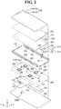
- FIG. 2 is an exploded, perspective view of a display device according to some exemplary embodiments.
- a display device 10 includes a cover window 100, a touch sensing device 200, a touch circuit board 210, a touch driver 220, a display panel 300, a display circuit board 310, a display driver 320, a first waterproof member 410, a second waterproof member 420, a third waterproof member 430, a fourth waterproof member 440, a first electromagnetic wave shielding member 450, a second electromagnetic wave shielding member 460, a third electromagnetic wave shielding member 470, a fourth electromagnetic wave shielding member 480, a first force sensor 510, a second force sensor 520, a middle frame 600, a main circuit board 700, a first vibration generator 810, a second vibration generator 820, a third vibration generator 830, a fourth vibration generator 840, and a bottom cover 900.
- the terms “above,” “top,” and “upper surface” refer to the side of the display panel 300 in the z-axis direction where the cover window 100 is disposed, whereas the terms “below,” “bottom,” and “lower surface” refer to the opposite side of the display panel 300 in the z-axis direction where the middle frame 600 is disposed.
- the terms “left,” “right,” “upper,” and “lower” indicate relative positions when the display panel 300 is viewed from the top.
- the "left side” refers to the opposite direction indicated by the arrow of the x-axis
- the “right side” refers to the direction indicated by the arrow of the x-axis
- the "upper side” refers to the direction indicated by the arrow of the y-axis
- the “lower side” refers to the opposite direction indicated by the arrow of the y-axis.
- the display device 10 may have a rectangular shape when viewed from the top.
- the display device 10 may have a rectangular shape having shorter sides in a first direction (e.g., the x-axis direction) and longer sides in a second direction (e.g., the y-axis direction) when viewed from the top as shown in FIGS. 1 and 2 .
- Each of the corners where the short side in the first direction (x-axis direction) meets the longer side in the second direction (y-axis direction) may be rounded with a predetermined curvature or may be a right angle.
- the shape of the display device 10 when viewed from the top is not limited to a rectangular shape, but may be formed in another polygonal shape, circular shape, elliptical shape, etc.
- the display device 10 may include a first area DR1 which is formed flat, and second areas DR2 extended from the right and left sides of the first area DR1.
- the second areas DR2 may be formed flat or may be curved.
- the angle formed by the first area DR1 and the second areas DR2 may be an obtuse angle.
- the second areas DR2 are formed as curved surfaces, they may have a constant curvature or a varying curvature.
- the second areas DR2 are extended from the left and right sides of the first area DR1 in FIG. 1 , this is merely illustrative. That is to say, the second area DR2 may be extended from only one of the right and left sides of the first area DR1. As another example, the second area DR2 may be extended from at least one of the upper and lower sides of the first area DR1, as well as (or as an alternative to) the left and right sides. In the following description, the second areas DR2 disposed at the left and right edges of the display device 10, respectively, will be described as an example.
- the cover window 100 may be disposed on the display panel 300 to cover the upper surface of the display panel 300. Thus, the cover window 100 can protect the upper surface of the display panel 300.
- the cover window 100 may be attached to the touch sensing device 200 through a first adhesive member 910 as shown in FIG. 13 .
- the first adhesive member 910 may be an optically cleared adhesive film (OCA) or an optically cleared resin (OCR).
- the cover window 100 may include a transmissive portion DA100 corresponding to the display panel 300 and a non-transmissive portion NDA100 corresponding to another area other than the display panel 300.
- the cover window 100 may be disposed in the first area DR1 and the second areas DR2, and the transmissive portion DA100 may be disposed in a part of the first area DR1 and a part of the second areas DR2.
- the non-transmissive portion NDA100 may be opaque.
- the non-transmissive portion NDA100 may be formed as a decoration layer having a pattern that can be displayed to the user when no image is displayed. For example, a company's logo, such as "SAMSUNG,” or various letters may be patterned in the non-transmissive portion NDA100.
- Holes HH for exposing various components may be formed in the non-transmissive portion NDA100 of the cover window 100.
- a front camera, a front speaker, an infrared sensor, an ultrasonic sensor, an illuminance sensor, etc. may be formed in the non-transmissive portion NDA100 of the cover window 100.
- some or all of the front camera, the front speaker, the infrared sensor, the ultrasonic sensor, and the illuminance sensor may be incorporated into (or as part of) the display panel 300, in which case some or all of the holes HH may be removed.
- the cover window 100 may be made of any suitable material, such as glass, sapphire, and/or plastic.
- the cover window 100 may be rigid and/or flexible.
- the touch sensing device 200 may be disposed between the cover window 100 and the display panel 300.
- the touch sensing device 200 may be disposed in the first area DR1 and the second areas DR2. Therefore, a user's touch (or touch interaction) can be detected not only in the first area DR1, but also in the second areas DR2.
- the touch sensing device 200 may be attached to the lower surface of the cover window 100 through the first adhesive member 910.
- a polarizing film (not shown) may be added on the touch sensing device 200 to avoid decreasing visibility otherwise due to reflection of external light.
- the polarizing film may be attached to the lower surface of the cover window 100 through the first adhesive member 910.
- the touch sensing device 200 is an element for sensing a user's touch position.
- the touch sensing device 200 may be implemented as a capacitive touch sensing device of a self-capacitance type or a mutual capacitance type.
- the touch sensing device 200 may include only touch driving electrodes.
- the touch sensing device 200 is of a mutual capacitance type, the touch sensing device 200 may include touch driving electrodes and touch sensing electrodes.
- a mutual capacitive type touch sensing device will be described as an example.
- the touch sensing device 200 may be in the form of panel or film.
- the touch sensing device 200 may be attached to a thin-film encapsulation layer (not shown) of the display panel 300 through the second adhesive member 920 as shown in FIG. 13 .
- the second adhesive member 920 may be a transparent adhesive film (OCA) or a transparent adhesive resin (OCR).
- the touch sensing device 200 may be formed integrally with the display panel 300.
- the touch driving electrodes and the touch sensing electrodes of the touch sensing device 200 may be formed on the thin-film encapsulation layer of the display panel 300.
- a touch circuit board 210 may be attached to one side of the touch sensing device 200.
- the touch circuit board 210 may be attached to pads disposed on one side of the touch sensing device 200 using an anisotropic conductive film.
- a touch connection portion may be provided at one end of the touch circuit board 210, and the touch connection portion may be connected to the connector of the display circuit board 310.
- the touch circuit board may be a flexible printed circuit board.
- the touch driver 220 may apply touch driving signals to the touch driving electrodes of the touch sensing device 200, may sense sensing signals from the touch sensing electrodes of the touch sensing device 200, and may calculate (or determine) a user's touch position by analyzing the sensing signals.
- the touch driver 220 may be formed as an integrated circuit and mounted on the touch circuit board 210.
- the display panel 300 may be disposed under the touch sensing device 200.
- the display panel 300 may overlap the transmissive portion DA100 of the cover window 100.
- the display panel 300 may be disposed in the first area DR1 and the second areas DR2. As such, an image on the display panel 300 may be seen not only in the first area DR1, but also in the second areas DR2.
- the display panel 300 may be a light-emitting display panel including a light-emitting element; however, exemplary embodiments are not limited thereto.
- the display panel 300 may include an organic light-emitting display panel using organic light-emitting diodes, a micro light-emitting diode display panel using micro light-emitting diodes, and a quantum-dot light-emitting display panel including quantum-dot light-emitting diodes.
- the display panel 300 may include a substrate, a thin-film transistor layer disposed on the substrate, a light-emitting element layer, and a thin-film encapsulation layer.
- the substrate may include a flexible substrate and a support substrate. Because the support substrate supports the flexible substrate, it may be less flexible than the substrate.
- Each of the flexible substrate and the support substrate may include a flexible polymer material; however, any suitable material may be utilized.
- each of the flexible substrate and the support substrate may be polyethersulfone (PES), polyacrylate (PA), polyacrylate (PAR), polyetherimide (PEI), polyethylene naphthalate (PEN), polyethylene terephthalate (PET), polyphenylene sulfide (PPS), polyallylate, polyimide (PI), polycarbonate (PC), cellulose triacetate (CAT), cellulose acetate propionate (CAP), etc., or any suitable combination thereof.
- PES polyethersulfone
- PA polyacrylate
- PAR polyacrylate
- PEI polyetherimide
- PEN polyethylene naphthalate
- PET polyethylene terephthalate
- PPS polyphenylene sulfide
- PI polyimide
- PC polycarbonate
- CAT cellulose triacetate
- CAP cellulose acetate propionate
- a thin-film transistor layer is disposed on the substrate.
- the thin-film transistor layer may include scan lines, data lines, and thin-film transistors.
- Each of the thin-film transistors includes a gate electrode, a semiconductor layer, and source and drain electrodes.
- a scan driver When a scan driver is formed directly on the substrate, it may be formed together with the thin-film transistor layer.
- the light-emitting element layer is disposed on the thin-film transistor layer.
- the light-emitting element layer includes anode electrodes, an emissive layer, a cathode electrode, and banks.
- the emissive layer may include an organic emissive layer containing an organic material.
- the emissive layer may include a hole injection layer, a hole transporting layer, an organic light-emitting layer, an electron transporting layer, and an electron injection layer. The hole injection layer and the electron injection layer may be omitted.
- the light-emitting element layer may be a pixel array layer where pixels are formed. Accordingly, the region where the light-emitting element layer is formed may be defined as a display area for displaying images.
- the peripheral area of the display area may be defined as a non-display area.
- An encapsulation layer (or thin film encapsulation layer) is disposed on the light-emitting element layer.
- the encapsulation layer serves to prevent permeation of oxygen or moisture into the light-emitting element layer.
- the encapsulating layer may include at least one inorganic layer and at least one organic layer.
- the display circuit board 310 may be attached to one side of the display panel 300.
- the display circuit board 310 may be attached to pads disposed on one side of the display panel 300 using an anisotropic conductive film.
- the touch circuit board 210 may also be bent toward the lower surface of the display panel 300, and the touch connection portion disposed at one end of the touch circuit board 210 may be connected to the connector of the display circuit board 310.
- the display circuit board 310 will be described in more detail with reference to FIGS. 3 and 4 .
- the display driver 320 outputs signals and voltages for driving the display panel 300 through the display circuit board 310.
- the display driver 320 may be formed as an integrated circuit and mounted on the display circuit board 310, but is not limited thereto.
- the display driver 320 may be attached to one side of the upper surface or the lower surface of the substrate of the display panel 300.
- a panel support member 390 may be disposed under the display panel 300 as shown in FIG. 13 .
- the panel support member 390 may be attached to the lower surface of the display panel 300 through a third adhesive member 930.
- the third adhesive member 930 may be a transparent adhesive film (OCA) or a transparent adhesive resin (OCR).
- the panel support member 390 may include at least one of a light-absorbing member for absorbing light incident from outside, a buffer member for absorbing external impact, a heat dissipating member for efficiently discharging heat from the display panel 300, and a light-blocking layer for blocking light incident from outside.
- the light-absorbing member may be disposed under the display panel 300.
- the light-absorbing member blocks the transmission of light to prevent elements disposed under the light-absorbing member from being seen from above the display panel 300, such as the first waterproof member 410, the first force sensor 510, the second waterproof member 420, the second force sensor 520, and the display circuit board 310.
- the light-absorbing member may include a light absorbing material, such as a black pigment or a dye.
- the buffer member may be disposed under the light-absorbing member.
- the buffer member absorbs an external impact to prevent (or at least reduce the likelihood of) the display panel 300 from being damaged.
- the buffer member may be made up of a single layer or multiple layers.
- the buffer member may be formed of a polymer resin, such as polyurethane, polycarbonate, polypropylene, polyethylene, etc., or may be formed of a material having elasticity, such as a rubber and a sponge obtained by foaming a urethane-based material or an acrylic-based material.
- the buffer member may be a cushion layer.
- the heat dissipating member may be disposed under the buffer member.
- the heat dissipation member may include a first heat dissipation layer including graphite or carbon nanotubes, and a second heat dissipation layer formed of a thin metal film, such as copper, nickel, ferrite, silver, etc., which can block electromagnetic waves and have high thermal conductivity.
- the first waterproof member 410, the second waterproof member 420, the first force sensor 510, and the second force sensor 520 may be disposed in the second area DR2. That is to say, the first waterproof member 410 and the first force sensor 510 may be disposed under the display panel 300 at the right edge (or side portion) of the display panel 300. The second waterproof member 420 and the second force sensor 520 may be disposed under the display panel 300 at the left edge (or side portion) of the display panel 300. The first force sensor 510 may face the second force sensor 520, and the first waterproof member 410 may face the second waterproof member 420.
- the first force sensor 510 may be attached to the lower surface of the panel support member 390.
- the first waterproof member 410 may be attached to the lower surface of the first force sensor 510. Additionally, the first waterproof member 410 may be attached to at least one side of the first force sensor 510 so as to prevent (or at least reduce) moisture or dust from permeating between the display panel 300 and the first force sensor 510. At least one side of the first force sensor 510 may be a side adjacent to the right edge of the display panel 300.
- the second force sensor 520 may be attached to the lower surface of the panel support member 390.
- the second waterproof member 420 may be attached to the lower surface of the second force sensor 520. Additionally, the second waterproof member 420 may be attached to at least one side of the second force sensor 520 so as to prevent (or at least reduce) moisture or dust from permeating between the display panel 300 and the second force sensor 520. At least one side of the second force sensor 520 may be a side adjacent to the left edge of the display panel 300.
- the third waterproof member 430 is disposed under the display panel 300 at the upper edge (or side portion) of the display panel 300.
- the fourth waterproof member 440 is disposed under the display panel 300 at the lower edge (or side portion) of the display panel 300.
- the third waterproof member 430 may face the fourth waterproof member 440.
- the height of the first waterproof member 410 and the height of the second waterproof member 420 may be greater than the height of the third waterproof member 430 or the height of the fourth waterproof member 440.
- a waterproof resin layer may be formed between the first waterproof member 410 and the third waterproof member 430, between the first waterproof member 410 and the fourth waterproof member 440, between the second waterproof member 420 and the third waterproof member 430, and between the second waterproof member 420 and the fourth waterproof member 440.
- Each of the first waterproof member 410, the second waterproof member 420, the third waterproof member 430, and the fourth waterproof member 440 includes a base film, a first adhesive film disposed on a surface of the base film, and a second adhesive film disposed on the other surface of the base film.
- the base film may be a polyethylene terephthalate (PET), a polyethylene terephthalate (PET), and a cushion layer, or a polyethylene foam (PE-foam).
- the first adhesive film and the second adhesive film may be pressure sensitive adhesive (PSA).
- the edges of the lower surface of the display panel 300 are attached to the edges of the upper surface of the middle frame 600 by the first waterproof member 410, the second waterproof member 420, the third waterproof member 430 and the fourth waterproof member 440. Accordingly, it is possible to prevent (or at least reduce) moisture and dust from permeating between the display panel 300 and the middle frame 600. That is to say, the display device 10 with waterproof and dustproof capabilities can be produced.
- the first force sensor 510 and the second force sensor 520 may be connected to the display circuit board 310 via a third circuit board 550 (see FIG. 8 ).
- FIGS. 3 and 8 show that the first force sensor 510 and the second force sensor 520 are connected to the third circuit board 550, exemplary embodiments are not limited thereto.
- the display device 10 may include more than one third circuit board 550, such that the first force sensor 510 may be connected to the display circuit board 310 via one third circuit board 550, and the second force sensor 520 may be connected to the display circuit board 310 via another third circuit board 550.
- a force sensing unit 330 for sensing the force by driving the first force sensor 510 and the second force sensor 520 may be mounted on the display circuit board 310.
- the force sensing unit 330 may be implemented as an integrated circuit.
- the force sensing unit 330 may be integrated with the display driver 320 to form a single integrated circuit.
- the third circuit board 550 may be connected to the touch circuit board 210 rather than the display circuit board 310. Then, the force sensing unit 330 may be mounted on the touch circuit board 210. The force sensing unit 330 may be integrated with the touch driver 220 to form a single integrated circuit.
- the middle frame 600 may be disposed below the panel support member 390.
- the middle frame 600 may include a synthetic resin, a metal, or both a synthetic resin and a metal.
- a first camera hole CMH1 for inserting a camera device 720, a battery hole BH for dissipating heat from a battery, and a cable hole CAH through which a second connection cable 314 connected to the display circuit board 310 passes.
- the cable hole CAH may be disposed in the second area DR2.
- the cable hole CAH may be disposed at (or near) the right edge of the middle frame 600, and may be covered by the first waterproof member 410 and the first force sensor 510 disposed under the display panel 300 at the right edge of the display panel 300.
- the first waterproof member 410 and the first force sensor 510 may include depressions NTH in the form of a notch for exposing the cable hole CAH as shown in FIG. 2 .
- the middle frame 600 is disposed below the panel support member 390 of the display panel 300, the first waterproof member 410, the second waterproof member 420, the third waterproof member 430, the fourth waterproof member 440, the first force sensor 510, and the second force sensor 520. Accordingly, the middle frame 600 can support the first force sensor 510 and the second force sensor 520 when a pressure is applied to at least one of the first force sensor 510 and the second force sensor 520. Accordingly, the first force sensor 510 and the second force sensor 520 can sense the applied force.
- the plurality of vibration generators may be disposed on the middle frame 600.
- the side surfaces of each of the plurality of vibration generators may be surrounded by the electromagnetic wave shielding members (e.g., first to fourth electromagnetic wave shielding members 450, 460, 470, and 480).
- the electromagnetic wave shielding members e.g., first to fourth electromagnetic wave shielding members 450, 460, 470, and 480.
- four vibration generators are disposed on the middle frame 600 for convenience of illustration, but exemplary embodiments are not limited thereto.
- the first vibration generator 810, the second vibration generator 820, the third vibration generator 830, and the fourth vibration generator 840 are disposed on the middle frame 600, e.g., disposed on the upper surface of the middle frame 600.
- the first vibration generator 810 and the third vibration generator 830 may be disposed adjacent to the first force sensor 510
- the second vibration generator 820 and the fourth vibration generator 840 may be disposed adjacent to the second force sensor 520.
- the first force sensor 510 may be disposed closer to a first side end of the display panel 300 or the middle frame 600 than the first vibration generator 810 and the third vibration generator 830.
- the second force sensor 520 may be disposed closer to a second side end of the display panel 300 or the middle frame 600 than the second vibration generator 820 and the fourth vibration generator 840.
- the first side of the display panel 300 or the middle frame 600 may be the right side, whereas the second side of the display panel 300 or the middle frame 600 may be the left side.
- the first vibration generator 810 may be disposed closer to the upper side than the third vibration generator 830, and the second vibration generator 820 may be disposed closer to the upper side than the fourth vibration generator 840.
- the first vibration generator 810, the second vibration generator 820, the third vibration generator 830, and the fourth vibration generator 840 may be connected to a vibration driver 340 of the display circuit board 310 via the fourth circuit board 890.
- the first vibration generator 810, the second vibration generator 820, the third vibration generator 830, and the fourth vibration generator 840 are connected to a single fourth circuit board 890 in FIG. 4 , exemplary embodiments are not limited thereto. That is to say, the display device 10 may include more than one fourth circuit board 890, and the first vibration generator 810, the second vibration generator 820, the third vibration generator 830, and the fourth vibration generator 840 may be connected to the display circuit board 310 through different fourth circuit boards 890, respectively.
- two of the first vibration generator 810, the second vibration generator 820, the third vibration generator 830, and the fourth vibration generator 840 may be connected to the display circuit board 310 via one fourth circuit board 890, and the other two of the first vibration generator 810, the second vibration generator 820, the third vibration generator 830, and the fourth vibration generator 840 may be connected to the display circuit board 310 via another fourth circuit board 890.
- the vibration driver 340 for driving the first vibration generator 810, the second vibration generator 820, the third vibration generator 830, and the fourth vibration generator 840 may be mounted on the display circuit board 310.
- the vibration driver 340 may be formed as an integrated circuit.
- the vibration driver 340 may be mounted on the fourth circuit board 890.
- the vibration driver 340 may generate first driving voltages and second driving voltages for driving each of the first vibration generator 810, the second vibration generator 820, the third vibration generator 830, and the fourth vibration generator 840 in response to vibration data received from a main processor 710.
- the vibration data from the main processor 710 may be transmitted to the vibration driver 340 via the second connection cable 314 of the main circuit board 700 and the display circuit board 310, the second circuit board 312, the first connection cable 313, and the first circuit board 311.
- the first driving voltages and the second driving voltages of the vibration driver 340 may be applied to the first vibration generator 810, the second vibration generator 820, the third vibration generator 830, and the fourth vibration generator 840 via the first circuit board 311 and the fourth circuit board 890 of the display circuit board 310.
- the vibration driver 340 may include a digital signal processor (DSP) for processing the vibration data, which is a digital signal, a digital-analog converter (DAC) for converting the vibration data processed by the digital signal processor in the form of a digital signal into the first driving voltages and the second driving voltages in the form of an analog signal, and an amplifier (AMP) for amplifying the first driving voltages and the second driving voltages converted by the digital-analog converter in the form of an analog signal to output the amplified first driving voltages and the amplified second driving voltages.
- DSP digital signal processor
- DAC digital-analog converter
- AMP amplifier
- the main processor 710 may control the first to fourth vibration generators 810, 820, 830, and 840 so that they have different vibration intensities and/or vibration cycles.
- the first vibration generator 810 may vibrate with the highest intensity
- the second vibration generator 820 may vibrate with the second highest intensity
- the third vibration generator 830 may vibrate with the third highest intensity
- the fourth vibration generator 840 may vibrate with the lowest intensity.
- the first vibration generator 810 may vibrate with the highest cycle
- the second vibration generator 820 may vibrate with the second highest cycle
- the third vibration generator 830 may vibrate with the third highest cycle
- the fourth vibration generator 840 may vibrate with the lowest cycle.
- each of the first vibration generator 810, the second vibration generator 820, the third vibration generator 830, and the fourth vibration generator 840 may be implemented as a sound generator that can generate sound by vibration.
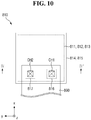
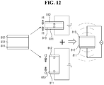
- the first vibration generator 810, the second vibration generator 820, the third vibration generator 830, and the fourth vibration generator 840 will be described in more detail with reference to FIGS. 10 to 12 .
- the first electromagnetic wave shielding member 450 may be disposed to surround the side surfaces of the first vibration generator 810 to prevent vibration generated by the first vibration generator 810 from propagating.
- the second electromagnetic wave shielding member 460 may be disposed to surround the side surfaces of the second vibration generator 820 to prevent vibration generated by the second vibration generator 820 from propagating.
- the third electromagnetic wave shielding member 470 may be disposed to surround the side surfaces of the third vibration generator 830 to prevent vibration generated by the third vibration generator 830 from propagating.
- the fourth electromagnetic wave shielding member 480 may be disposed to surround the side surfaces of the fourth vibration generator 840 to prevent vibration generated by the fourth vibration generator 840 from propagating.
- the first vibration generator 810 has a rectangular shape when viewed from the top and the first electromagnetic wave shielding member 450 surrounds all of the side surfaces of the first vibration generator 810; however, exemplary embodiments are not limited thereto.
- the first electromagnetic wave shielding member 450 may be disposed to surround two side surfaces of the first vibration generator 810.
- the first electromagnetic wave shielding member 450 may be disposed to surround three side surfaces of the first vibration generator 810.
- Each of the second to fourth electromagnetic wave shielding members 460, 470, and 480 may also be formed to surround two, three, or all side surfaces of the respective second to fourth vibration generators 820, 830, and 840 substantially in the same manner as the first vibration generator 810 depending on where the respective second to fourth vibration generators 820, 830, and 840 are disposed.
- vibration generated by the first vibration generator 810 can be blocked by the first electromagnetic wave shielding member 450. Accordingly, when the first vibration generator 810 vibrates, a user can feel the vibration only at the position where the first vibration generator 810 is disposed. Likewise, the user may feel vibration generated by the second vibration generator 820, vibration generated by the third vibration generator 830, or vibration generated by the fourth vibration generator 840 only at the position where the respective second to fourth vibration generators 820, 830, and 840 are disposed.
- the main circuit board 700 may be disposed under the middle frame 600.
- the main circuit board 700 may be a printed circuit board or a flexible printed circuit board.
- the main circuit board 700 may include a main processor 710, a camera device 720, a main connector 730, a fifth vibration generator 740, and a fifth electromagnetic wave shielding member 750.
- the main processor 710 may be disposed on the surface of the main circuit board 700 facing the middle frame 600, whereas the main connector 730 may be disposed on the other surface of the main circuit board 700 facing the bottom cover 900.
- the camera device 720 may be disposed on either surface of the main circuit board 700 such that the upper surface of the camera device 720 is disposed on the other surface of the main circuit board 700, and the lower surface of the camera device 720 is disposed on one surface of the main circuit board 700.
- the main processor 710 may control all or some of the functions of the display device 10. For example, the main processor 710 may output image data to the display driver 320 of the display circuit board 310 so that the display panel 300 displays an image. In addition, the main processor 710 may receive touch data from the touch driver 220 to determine the position of the user's touch, and may execute an application indicated by an icon displayed at the position of the user's touch. In addition, the main processor 710 may receive force sensing data from the touch driver 220 or the display driver 320 and may output a home screen, may control the volume of sound of the display device 10, may achieve haptic feedback in response to the force sensing data, and/or the like.
- the main processor 710 may output to the vibration driver 340 vibration data for vibrating the first vibration generator 810, the second vibration generator 820, the third vibration generator 830, and/or the fourth vibration generator 840, and may output the vibration signal for vibrating the fifth vibration generator 740.
- the main processor 710 may be an application processor, a central processing unit, or a system chip implemented as an integrated circuit.
- the camera device 720 processes image frames, such as still image and video obtained by the image sensor in the camera device 720, and outputs the image frames to the main processor 710.
- the second connection cable 314 passing through the cable hole CAH of the middle frame 600 may be connected to the main connector 730 disposed on the lower surface of the main circuit board 700 via a gap GAP between the middle frame 600 and the main circuit board 700. Accordingly, the main circuit board 700 may be electrically connected to the display circuit board 310 and the touch circuit board 210.
- the fifth vibration generator 740 may be a vibration generator, such as an eccentric rotating mass (ERM), a linear resonant actuator (LRA), or a piezo actuator.
- the fifth vibration generator 740 may generate vibration in response to a vibration signal received from the main processor 710.
- the fifth vibration generator 740 is disposed on (or near) the upper edge of the main circuit board 700 in FIG. 2 , exemplary embodiments are not limited thereto.
- the fifth electromagnetic wave shielding member 750 may be disposed to surround the side surfaces of the fifth vibration generator 740 to prevent vibration generated by the fifth vibration generator 740 from propagating.
- the fifth electromagnetic wave shielding member 750 shown in FIG. 2 surrounds all the side surfaces of the fifth vibration generator 740, but exemplary embodiments are not limited thereto.
- the fifth electromagnetic wave shielding member 750 may be disposed to surround two side surfaces of the fifth vibration generator 740.
- the fifth electromagnetic wave shielding member 750 may be disposed to surround three side surfaces of the fifth vibration generator 740.
- the fifth electromagnetic wave shielding member 750 may be made of a waterproof member (or material), such as at least one of plastic, steel, and a waterproof tape. In order to block (e.g., effectively block) the vibration by the fifth vibration generator 740 by the fifth electromagnetic wave shielding member 750, the fifth electromagnetic wave shielding member 750 may be disposed on the upper surface of the main circuit board 700 and the lower surface of the middle frame 600.
- a mobile communications module capable of transmitting/receiving a wireless signal to/from at least one of a base station, an external terminal, and a server over a mobile communications network may be further mounted on the main circuit board 700.
- the wireless signal may include various types of data depending on a voice signal, a video call signal, and/or a text/multimedia message transmission/reception.
- an acoustic output device capable of outputting sound, and a vibration generator capable of generating vibration for haptic feedback may be further mounted on the main circuit board 700.
- the bottom cover 900 may be disposed below the middle frame 600 and the main circuit board 700.
- the bottom cover 900 may be fastened and fixed to the middle frame 600.
- the bottom cover 900 may form the exterior of the lower surface of the display device 10.
- the bottom cover 900 may include plastic and/or metal.
- a second camera hole CMH2 may be formed in the bottom cover 900 through which the camera device 720 may be inserted to protrude to the outside.
- the positions of the camera device 720 and the first and second camera holes CMH1 and CMH2 in line with the camera device 720 are not limited to those shown in FIGS. 1-5 .
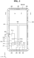
- FIG. 3 is a bottom view of a display panel attached a cover window according to some exemplary embodiments.
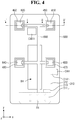
- FIG. 4 is a plan view of a middle frame according to some exemplary embodiments.
- FIG. 5 is a bottom view of a middle frame and a main circuit board according to some exemplary embodiments.
- FIG. 4 is a plan view
- FIGS. 3 and 5 are bottom views, and, as such, the left and right of the display device 10 in FIG. 4 are reversed in FIGS. 3 and 5 .
- the display circuit board 310 is depicted with a dashed line in FIG. 4
- the second connection cable 314 is depicted in a circle with a dot-dash line in FIG. 5 .
- the display circuit board 310 may include a first circuit board 311, a second circuit board 312, and a first connection cable 313.
- the first circuit board 311 may be attached to one side of the upper surface or the lower surface of the substrate of the display panel 300 and may be bent toward the lower surface of the substrate of the display panel 300.
- the first circuit board 311 may be fixed in the fixing holes FH formed in the middle frame 600 by fixing members as shown in FIG. 4 .
- the first circuit board 311 may include a display driver 320, a force sensing unit 330, a first connector 311a, a second connector 311b, and a third connector 311c.
- the display driver 320, the force sensing unit 330, the first connector 311a, the second connector 311b, and the third connector 311c may be disposed on the surface of the first circuit board 311.
- the first connector 311a may be connected to one end of the first connection cable 313 connected to the second circuit board 312.
- the display driver 320 and the force sensing unit 330 mounted on the first circuit board 311 may be electrically connected to the second circuit board 312 via the first connection cable 313.
- the second connector 311b may be connected to one end of the third circuit board 550 connected to the first force sensor 510 and the second force sensor 520. Accordingly, the first force sensor 510 and the second force sensor 520 may be electrically connected to the force sensing unit 330.
- the third connector 311c may be connected to one end of the fourth circuit board 890 connected to the first vibration generator 810, the second vibration generator 820, the third vibration generator 830, and the fourth vibration generator 840. Accordingly, each of the first vibration generator 810, the second vibration generator 820, the third vibration generator 830, and the fourth vibration generator 840 may be electrically connected to the vibration driver 340 of the display circuit board 310. Further, since the display circuit board 310 is electrically connected to the main circuit board 700 via the second connection cable 314, the first vibration generator 810, the second vibration generator 820, the third vibration generator 830, and the fourth vibration generator 840 may be electrically connected to the main processor 710 of the main circuit board 700.
- the second circuit board 312 may include a touch connector 312a, a first connector 312b, and a second connector 312c.
- the first connector 312b and the second connector 312c may be disposed on one surface of the second circuit board 312, and the touch connector 312a may be disposed on the other surface of the second circuit board 312.
- the touch connector 312a may be connected to one end of the touch circuit board 210. Accordingly, the touch driver 220 may be electrically connected to the second circuit board 312.
- the first connector 312b may be connected to the other end of the first connection cable 313 connected to the first circuit board 311.
- the display driver 320 and the force sensing unit 330 mounted on the first circuit board 311 may be electrically connected to the second circuit board 312 via the first connection cable 313.
- the second connector 312c may be connected to one end of a second connection cable 314 connected to the main connector 730 of the main circuit board 700.
- the second circuit board 312 may be electrically connected to the second circuit board 312 through the second connection cable 314.
- a connecting portion 315 may be formed at the other end of the second connection cable 314.
- the connecting portion 315 of the second connection cable 314 may be extended to the lower surface of the middle frame 600 through the cable hole CAH of the middle frame 600 as shown in FIGS. 4 and 5 .
- a depression NTH in the form of notch is formed in line with the cable hole CAH of the middle frame 600. Accordingly, the cable hole CAH of the middle frame 600 can be exposed without being covered by the first waterproof member 410 and the first force sensor 510.
- a gap GAP between the middle frame 600 and the main circuit board 700 is created in line with the cable hole CAH of the middle frame 600. Accordingly, the connecting portion 315 of the second connection cable 314, which has passed through the cable hole CAH, comes out through the gap GAP between the middle frame 600 and the main circuit board 700, to be extended to the lower surface of the main circuit board 700. In this manner, the connecting portion 315 of the second connection cable 314 may be connected to the main connector 730 disposed on the lower surface of the main circuit board 700.
- a depression NTH in the form of notch is formed in the first waterproof member 410 and the first force sensor 510 so as not to cover the cable hole CAH of the middle frame 600.
- the second connection cable 314 connected to the display circuit board 310 may be extended to the rear surface of the middle frame 600 through the cable hole CAH and may be connected to the main connector 730 of the main circuit board 700.
- the display circuit board 310 can be stably connected to the main circuit board 700.
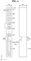
- FIG. 6 is a plan view of a first force sensor, first bumps, and a first waterproof member according to some exemplary embodiments.
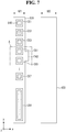
- FIG. 7 is a plan view of a second force sensor, second bumps, and a first waterproof member according to some exemplary embodiments.
- the first force sensor 510 may have a rectangular shape having shorter sides in a first direction (x-axis direction) and longer sides in a second direction (y-axis direction) when viewed from the top, e.g., in a third direction (z-axis direction); however, exemplary embodiments are not limited thereto.
- the shape of the first force sensor 510 may vary depending on where it is disposed.
- the first force sensor 510 includes a plurality of force detection cells CE1 to CE8. Although the first force sensor 510 shown in FIG. 6 includes eight force detection cells CE1 to CE8, the number of the force detection cells CE1 to CE8 is not limited to eight. Any suitable number of force detection cells may be utilized in association with exemplary embodiments.
- Each of the force detection cells CE1 to CE8 may individually sense force at their respective positions. Although the force detection cells CE1 to CE8 shown in FIG. 6 are arranged in a single row, exemplary embodiments are not limited thereto. The force detection cells CE1 to CE8 may be arranged in several rows as desired or arranged in any other suitable manner. In addition, the force detection cells CE1 to CE8 may be arranged at predetermined intervals as shown in FIG. 6 or may be arranged continuously or variably.
- the force detection cells CE1 to CE8 may have different areas depending on the use.
- the first to seventh force detection cells CE1 to CE7 may be used as physical buttons, such as volume control buttons VB+ and VB- and a power button PB disposed on a side of the display device 10.
- the eighth force detection cell CE8 may be used as a button SB for sensing a user's squeezing force.
- the eighth force detection cell CE8 may be formed to have a larger area than the first to seventh force detection cells CE1 to CE7.
- the eighth force detection cell CE8 may be longer than the first to seventh force detection cells CE1 to CE7 in the longitudinal direction (y-axis direction) of the first force sensor 510.
- first to seventh force detection cells CE1 to CE7 used as physical buttons have the same area in FIG. 6
- exemplary embodiments are not limited thereto.
- the first to seventh force detection cells CE1 to CE7 may have different areas from one another.
- some of the first to seventh force detection cells CE1 to CE7 may have the same area, whereas others may have the same area, which is different from the area of the some of the force detection cells.
- First bumps 530 may be disposed on the first to eighth force detection cells CE1 to CE8, respectively, such that the first bumps 530 overlap with the first to eighth force detection cells CE1 to CE8, respectively.
- the first bumps 530 may be used to press the first to eighth force detection cells CE1 to CE8 when a user's force is applied.
- Each of the first bumps 530 may be smaller than the respective one of the first to eighth force detection cells CE1 to CE8.
- the area of each of the first bumps 530 may be proportional to the area of the respective one of the first to eighth force detection cells CE1 to CE8. For example, as shown in FIG. 6 , when the area of the eighth force detection cell CE8 is larger than the area of each of the first to seventh force detection cells CE1 to CE7, the area of the first bump 530 on the eighth force detection cell CE8 may be larger than the area of the each of the first bumps 530 on the first to seventh force detection cells CE1 to CE7.
- the first waterproof member 410 may be attached to the lower surface and one side surface of the first force sensor 510.
- the width W2 of the first waterproof member 410 in the width direction (x-axis direction) may be larger than the width W1 of the first force sensor 510 in the width direction (x-axis direction).
- the area of the first waterproof member 410 may be larger than the area of the first force sensor 510.
- a first depression NTH1 in the form of notch may be formed in the first waterproof member 410 in line with the cable hole CAH of the middle frame 600, and a second depression NTH2 in the form of notch may be formed in the first force sensor 510.
- the first depression NTH1 does not cover the second depression NTH2 taking into account the process error margin (e.g., manufacturing tolerances), and thus, the width W3 of the first depression NTH1 is larger than the width W4 of the second depression NTH2.
- the second force sensor 520, the second bumps 540, and the second waterproof member 420 shown in FIG. 7 are different from the first force sensor 510, the first bumps 530, and the first waterproof member 410 in that no depressions NTH are formed in the second force sensor 520 and the second waterproof member 420.
- the second force sensor 520 may include a pad area PAD, which is described in more detail in association with FIGS. 8 and 9 . Therefore, the second force sensor 520, the second bump 540, and the second waterproof member 420 will not be described to avoid redundancy.
- FIG. 8 is an enlarged, plan view of area A shown in FIG. 7 according to some exemplary embodiments.
- FIG. 9 is a cross-sectional view taken along sectional line III - III' of FIG. 8 according to some exemplary embodiments.
- the first force sensor 510 includes a first substrate SUB1, a second substrate SUB2, a driving line TL, first to eighth sensing lines RL1 to RL8, a driving pad TP, first to eighth sensing pads RP1 to RP8, and first to eighth force detection cells CE1 to CE8, where p is an integer equal to or greater than two.
- FIG. 8 shows only the fourth force detection cell CE4, the fifth force detection cell CE5, and the pad area PAD for convenience of illustration.
- the second substrate SUB2 is not shown for convenience of illustration.
- the first substrate SUB1 faces the second substrate SUB2.
- Each of the first substrate SUB1 and the second substrate SUB2 may include a material, such as polyethylene, polyimide, polycarbonate, polysulfone, polyacrylate, polystyrene, polyvinylchloride, polyvinyl alcohol, poly(norbornene), and polyester.
- each of the first substrate SUB1 and the second substrate SUB2 may be formed as a polyethylene terephthalate (PET) film or a polyimide film.
- the first to eighth force detection cells CE1 to CE8 are disposed between the first substrate SUB1 and the second substrate SUB2.
- the driving line TL, the first to eighth sensing lines RL1 to RL8, the driving pad TP, and the first to eighth sensing pads RP1 to RP8 are disposed on one surface of the first substrate SUB1 facing the second substrate SUB2.
- the first to eighth force detection cells CE1 to CE8 are disposed between the first substrate SUB1 and the second substrate SUB2.
- Each of the first to eighth force detection cells CE1 to CE8 may be connected to at least one driving line (e.g., driving line TL) and at least one sensing line (e.g., at least one of first to eighth sensing lines RL1 to RL8).
- driving line TL driving line
- sensing line e.g., at least one of first to eighth sensing lines RL1 to RL8
- the first to eighth force detection cells CE1 to CE8 may be commonly connected to a single driving line TL, they may be connected to the first to eighth sensing lines RL1 to RL8, respectively.
- the fourth force detection cell CE4 may be connected to the driving line TL and the fourth sensing line RL4
- the fifth force detection cell CE5 may be connected to the driving line TL and the fifth sensing line RL5.
- the driving line TL may be connected to the driving pad TP, and the first to eighth sensing lines RL1 to RL8 may be connected to the first to eighth sensing pads RP1 to RP8, respectively.
- the first sensing line RL1 may be connected to the first sensing pad RP1
- the second sensing line RL2 may be connected to the second sensing pad RP2
- the third sensing line RL3 may be connected to the third sensing pad RP3
- the fourth sensing line RL4 may be connected to the fourth sensing pad RP4.
- the fifth sensing line RL5 may be connected to the fifth sensing pad RP5
- the sixth sensing line RL6 may be connected to the sixth sensing pad RP6
- the seventh sensing line RL7 may be connected to the seventh sensing pad RP7
- the eighth sensing line RL8 may be connected to the eighth sensing pad RP8.
- the pad area PAD may protrude from one side of the first substrate SUB1.
- the side of the first substrate SUB1 may be the longer side of the first force sensor 510.
- the pad area PAD protrudes from the center of the longer side of the first substrate SUB1 in FIG. 8 , exemplary embodiments are not limited thereto.
- the pad area PAD may protrude from one end or the other end of the longer side of the first substrate SUB1.
- the driving pad TP and the first to eighth sensing pads RP1 to RP8 may be disposed in (or on) the pad area PAD.
- the driving pad TP and the first to eighth sensing pads RP1 to RP8 may be connected to a driving lead line TL_F and first to eighth sensing lead lines RL1_F to RL8_F of the third circuit board 550, respectively, through an anisotropic conductive film.
- the driving pad TP may be connected to the driving lead line TL_F
- the first sensing pad RP1 may be connected to a first sensing lead line RL1_F
- the second sensing pad RP2 may be connected to a second sensing lead line RL2_F
- the third sensing pad RP3 may be connected to a third sensing lead line RL3_F
- the fourth sensing pad RP4 may be connected to a fourth sensing lead line RL4_F.
- the fifth sensing pad RP5 may be connected to the fifth sensing lead line RP5_F
- the sixth sensing pad RP6 may be connected to the sixth sensing lead line RP6_F
- the seventh sensing pad RP7 may be connected to the seventh sensing lead line RP7_F
- the eighth sensing pad RP8 may be connected to the eighth sensing lead line RP8_F.
- the third circuit board 550 is connected to the display circuit board 310 so that the third circuit board 550 may be electrically connected to the force sensing unit 330 mounted on the display circuit board 310.
- the force sensing unit 330 applies a driving voltage to the driving line TL through the driving lead line TL_F of the third circuit board 550 and the driving pad TP of the first force sensor 510, and senses the current values or voltage values from the first to eighth sensing lines RL1 to RL8 through the first to eighth sensing lead lines RL1_F to RL8_F connected to the first to eighth sensing pads RP1 to RP8 of the first force sensor 510, to thereby sense force applied to the first to eighth force detection cells CE1 to CE8.
- the first force sensor 510 may further include a coupling layer (not shown) disposed between the first substrate SUB1 and the second substrate SUB2 to couple the first substrate SUB1 and the second substrate SUB2 together.
- the coupling layer may be implemented as a pressure-sensitive adhesive layer or an adhesive layer.
- the coupling layer may be disposed along the periphery of the first substrate SUB1 and the second substrate SUB2. In some exemplary embodiments, the coupling layer may completely surround the edges of the first substrate SUB1 and the second substrate SUB2 to seal the inside of the first force sensor 510.
- the coupling layer may serve as a spacer for maintaining a distance between the first substrate SUB1 and the second substrate SUB2.
- the coupling layer may not overlap with the driving line TL, the first to eighth sensing lines RL1 to RL8, the first to eighth force detection cells CE1 to CE8, the driving pad TP, or the first to eighth sensing pads RP1 to RP8.
- the coupling layer may be first attached to one surface of one of the first substrate SUB1 and the second substrate SUB2 and then attached to one surface of the other substrate during a process of attaching the first substrate SUB1 and the second substrate SUB2 together.
- a coupling layer may be disposed on each of one surface of the first substrate SUB1 and one surface of the second substrate SUB2, and then the coupling layer on the first substrate SUB 1 may be attached to the coupling layer on the second substrate SUB2 during a process of attaching the first substrate SUB1 and the second substrate SUB2 together.
- each of the first to eighth force detection cells CE1 to CE8 includes a driving connection electrode TCE, a sensing connection electrode RCE, driving electrodes TE1, sensing electrodes RE1, and a force sensing layer PSL.
- the driving connection electrode TCE, the sensing connection electrode RCE, the driving electrodes TE1, and the sensing electrodes RE1 are disposed on the first substrate SUB1 facing the second substrate SUB2.
- the driving connection electrode TCE is connected to the driving line TL and the driving electrode TE1.
- the driving connection electrode TCE is connected to the driving line TL at one end in the longitudinal direction (y-axis direction).
- the driving electrodes TE1 may branch off in the width direction (x-axis direction) of the driving connection electrode TCE.
- the sensing connection electrode RCE is connected to one of the first to eighth sensing lines RL1 to RL8 and the sensing electrodes RE1.
- the sensing connection electrode RCE is connected to one of the first to eighth sensing lines RL1 to RL8 at one end in the longitudinal direction (y-axis direction).
- the sensing electrodes RE1 may branch off in the width direction (x-axis direction) of the sensing connection electrode RCE.
- the driving electrodes TE1 and the sensing electrodes RE1 may be disposed on the same layer.
- the driving electrodes TE1 and the sensing electrodes RE1 may be made of the same material.
- the driving electrodes TE1 and the sensing electrodes RE1 may include a conductive material, such as silver (Ag) and copper (Cu); however, exemplary embodiments are not limited thereto.
- the driving electrodes TE1 and the sensing electrodes RE1 may be formed on the first substrate SUB1 by screen printing.
- the driving electrodes TE1 and the sensing electrodes RE1 are disposed adjacent to each other, but are not connected to each other.
- the driving electrodes TE1 and the sensing electrodes RE1 may be arranged in parallel with one another.
- the driving electrodes TE1 and the sensing electrodes RE1 may be alternately arranged in the longitudinal direction (y-axis direction) of the driving connection electrode TCE and the sensing connection electrode RCE. That is to say, the driving electrode TE1, the sensing electrode RE1, the driving electrode TE1, and the sensing electrode RE1 may be arranged repeatedly in this order in the longitudinal direction (y-axis direction) of the driving connection electrode TCE and the sensing connection electrode RCE.
- the force sensing layer PSL is disposed on the surface of the second substrate SUB2 facing the first substrate SUB1.
- the force sensing layer PSL may be disposed such that the force sensing layer PSL overlaps with the driving electrodes TE1 and the sensing electrodes RE1.
- the force sensing layer PSL may include a pressure sensitive material and a polymer resin where the pressure sensitive material is disposed.
- the pressure sensitive material may be metal micro-particles (or metal nanoparticles), such as nickel, aluminum, titanium, tin and copper; however, exemplary embodiments are not limited thereto.
- the force sensing layer PSL may be a quantum tunneling composite (QTC).
- the force sensing layer PSL When a force is applied to the second substrate SUB2 in the height direction (z-axis direction) of the first force sensor 510, the force sensing layer PSL may come in contact with the driving electrodes TE1 and the sensing electrodes RE1. In this case, at least one of the driving electrodes TE1 and at least one of the sensing electrodes RE1 may be physically connected through the force sensing layer PSL, and the force sensing layer PSL may work as an electrical resistance.
- the area in which the force sensing layer PSL comes in contact with the driving electrodes TE1 and with the sensing electrodes RE1 depends on the force applied to the first force sensor 510, such that the resistance value of the sensing line electrically connected to the sensing electrodes RE1 may vary.
- the force sensing unit 330 senses a change in current value or a voltage value from the first to eighth sensing lines RL1 to RL8, thereby sensing the applied force, e.g., a force that the user presses by hand.
- the second force sensor 520 is substantially identical to the first force sensor 510 shown in FIGS. 8 and 9 , and, therefore, a redundant description will be omitted.
- FIG. 10 is a plan view showing a first vibration generator according to some exemplary embodiments.
- FIG. 11 is a cross-sectional view taken along sectional line IV - IV' of FIG. 10 according to some exemplary embodiments.
- the first vibration generator 810 may include a first electrode 811, a second electrode 812, a vibration layer 813, a first base substrate 814, a second base substrate 815, a first pad electrode 816, and a second pad electrode 817.
- the first electrode 811 may be disposed on the first surface of the first base substrate 814, and the vibration layer 813 may be disposed on the first electrode 811.
- the second electrode 812 may be disposed on the vibration layer 813, and the second base substrate 815 may be disposed on the second electrode 812.
- the first pad electrode 816 and the second pad electrode 817 may be disposed on the second surface of the first base substrate 814.
- the first electrode 811 and the second electrode 812 may be made of a conductive material.
- the conductive material may be a transparent conductive material, such as indium tin oxide (ITO), indium zinc oxide (IZO), etc., an opaque metal material, a conductive polymer, a carbon nanotube (CNT), etc.
- the first electrode 811 may be connected to the first pad electrode 816 through a first contact hole CH1 penetrating the first base substrate 814, and accordingly may be connected to the fourth circuit board 890 through the first pad electrode 816.
- the second electrode 812 may be connected to the second pad electrode 817 through a second contact hole CH2 penetrating the vibration layer 813 and the first base substrate 814, and accordingly may be connected to the fourth circuit board 890 through the second pad electrode 817.
- the first electrode 811 and the second electrode 812 can be electrically connected to the vibration driver 340 of the display circuit board 310 through the fourth circuit board 890, thereby receiving the first driving voltage and the second driving voltage from the vibration driver 340.
- FIG. 12 is a view for illustrating an example of vibration of the first vibration generator of FIG. 10 according to some exemplary embodiments.
- the vibration layer 813 may be a piezo actuator that is deformed as shown in FIG. 12 according to the difference between the voltage applied to the first electrode 811 and the voltage applied to the second electrode 812.
- the vibration layer 813 may be at least one of a piezoelectric material, such as a poly vinylidene fluoride (PVDF) film, a plumbum zirconate titanate (PZT), etc., and an electroactive polymer.
- PVDF poly vinylidene fluoride
- PZT plumbum zirconate titanate
- the vibration layer 813 contracts according to a first force F1 or relaxes according to a second force F2 according to the difference between the first driving voltage applied to the first electrode 811 and the second driving voltage applied to the second electrode 812.
- a first force F1 or relaxes according to a second force F2 according to the difference between the first driving voltage applied to the first electrode 811 and the second driving voltage applied to the second electrode 812.
- the vibration layer 813 adjacent to the first electrode 811 has a positive polarity characteristic
- the vibration layer 813 adjacent to the second electrode 812 has a negative polarity characteristic
- the positive first driving voltage is applied to the first electrode 811
- the negative second driving voltage is applied to the second electrode 812, such that the vibration layer 813 may contract according to the first force F1.
- the vibration layer 813 adjacent to the first electrode 811 has a positive polarity characteristic and the vibration layer 813 adjacent to the second electrode 812 has a negative polarity characteristic
- the negative first driving voltage is applied to the first electrode 811 and the positive second driving voltage is applied to the second electrode 812, such that the vibration layer 813 may relax according to the second force F2.
- the vibration layer 813 repeatedly contracts and relaxes. As a result, the first vibration generator 810 vibrates.
- the first vibration generator 810 may also vibrate the display panel 300 to output a first sound.
- the display device 10 can output sound by the a sound generator not exposed to the outside, the sound generator disposed on the front surface of the display device 10 can be eliminated.
- the transmissive portion DA100 can be widened. That is to say, the display area of the display device 10 can be widened or enlarged.
- the first base substrate 814 and the second base substrate 815 may be made of an insulating material.
- each of the first base substrate 814 and the second base substrate 815 may be polyethersulfone (PES), polyacrylate (PA), polyacrylate (PAR), polyetherimide (PEI), polyethylene naphthalate (PEN), polyethylene terephthalate (PET), polyphenylene sulfide (PPS), polyallylate, polyimide (PI), polycarbonate (PC), cellulose triacetate (CAT), cellulose acetate propionate (CAP), or any suitable combination thereof.
- each of the first base substrate 814 and the second base substrate 815 may be made of a plastic material.
- the first pad electrode 816 and the second pad electrode 817 may be made of a conductive material.
- the first pad electrode 816 and the second pad electrode 817 may be connected to the fourth circuit board 890 using an anisotropic conductive film.
- Each of the second vibration generator 820, the third vibration generator 830, and the fourth vibration generator 840 is substantially identical to the first vibration generator 810 described above with reference to FIGS. 10 to 12 , and, therefore, a redundant description will be omitted.
- the first vibration generator 810, the second vibration generator 820, the third vibration generator 830, and the fourth vibration generator 840 may be attached to the upper surface of the middle frame 600 disposed under the display panel 300, and connected to the display circuit board 310 through the fourth circuit board 890.
- the first vibration generator 810, the second vibration generator 820, the third vibration generator 830, the fourth vibration generator 840, the fourth circuit board 890, and the middle frame 600 may be implemented as a single module together with the display panel 300.
- FIG. 13 is a cross-sectional view taken along sectional lines of I - I' and II - II' of FIGS. 3 and 4 according to some exemplary embodiments.
- the first force sensor 510 may be disposed in the second area DR2 corresponding to a curved portion of the display device 10.
- the first bumps 530 may be disposed on the upper surface of the first force sensor 510.
- Each of the first bumps 530 may be attached to the lower surface of the panel support member 390 under the display panel 300 through the fourth adhesive member 940. Exemplary embodiments, however, are not limited thereto.
- each of the first bumps 530 may be disposed on the lower surface of the first force sensor 510.
- the upper surface of the first force sensor 510 may be attached to the lower surface of the panel support member 390 under the display panel 300 through the fourth adhesive member 940. Exemplary embodiments, however, are not limited thereto.
- each of the first bumps 530 may be disposed on the lower surface of the first force sensor 510.
- the upper surface of the first force sensor 510 may be attached to the lower surface of the panel support member 390 under the display panel 300 through the fourth adhesive member 940.
- the fourth adhesive member 940 may be an optically cleared adhesive film (OCA) or an optically cleared resin (OCR).
- the first waterproof member 410 may be disposed on the lower surface of the first force sensor 510.
- the first waterproof member 410 may be attached to the lower surface of the first force sensor 510 and the upper surface of the middle frame 600.
- the first waterproof member 410 may be additionally attached to a side surface of the first force sensor 510 so as to prevent moisture or dust from permeating between the display panel 300 and the first force sensor 510.
- the upper surface of the first waterproof member 410 attached to one side surface of the first force sensor 510 may be attached to the lower surface of the panel support member 390 of the display panel 300.
- the fourth adhesive member 940 may be eliminated. Since the first force sensor 510 is disposed at (or near) the right edge of the display panel 300, one side surface of the first force sensor 510 may be the right side surface of the first force sensor 510.
- the first waterproof member 410 is attached to the lower surface and the right side surface of the first force sensor 510. Accordingly, even if the first force sensor 510 is disposed at the right edge on the lower surface of the panel support member 390, it is possible to prevent moisture and dust from permeating between the display panel 300 and the middle frame 600 by the first waterproof member 410. That is to say, the display device 10 with waterproof and dustproof capabilities can be produced.
- the first vibration generator 810 may be disposed in the first area DR1 corresponding to the flat portion of the display device 10.
- the first vibration generator 810 may be disposed adjacent to the first force sensor 510.
- the first vibration generator 810 may be attached to the upper surface of the middle frame 600 through the fifth adhesive member 950.
- the fifth adhesive member 950 may be an optically cleared adhesive film (OCA) or an optically cleared resin (OCR).
- the fourth circuit board 890 may be attached to the first vibration generator 810.
- the fourth circuit board 890 may be attached to the first pad electrode 816 and the second pad electrode 817 disposed on the upper surface of the first vibration generator 810.
- the first electromagnetic wave shielding member 450 may be disposed to surround the side surfaces of the first vibration generator 810.
- the first electromagnetic wave shielding member 450 shown in FIG. 4 surrounds all the side surfaces of the first vibration generator 810, but exemplary embodiments are not limited thereto.
- the first electromagnetic wave shielding member 450 may be disposed to surround two side surfaces of the first vibration generator 810.
- the first electromagnetic wave shielding member 450 may be disposed to surround three side surfaces of the first vibration generator 810.
- the first electromagnetic wave shielding member 450 may be formed of a waterproof member (or material) substantially identical to the first waterproof member 410.
- the first electromagnetic wave shielding member 450 may include a base film, a first adhesive layer disposed on a surface of the base film, and a second adhesive layer disposed on the other surface of the base film.
- the base film may be a polyethylene terephthalate (PET), a polyethylene terephthalate (PET), and a cushion layer, or a polyethylene foam (PE-foam).
- the first adhesive film and the second adhesive film may be pressure sensitive adhesive (PSA).
- the first electromagnetic wave shielding member 450 may be higher (extender further from the middle frame 600) than the first vibration generator 810. Accordingly, the first electromagnetic wave shielding member 450 may be attached to the lower surface of the panel support member 390 of the display panel 300 and the upper surface of the middle frame 600. When the fourth circuit board 890 is disposed on one side of the first vibration generator 810, the first electromagnetic wave shielding member 450 may be attached to the lower surface of the panel support member 390 and the fourth circuit board 890. As seen in FIG.
- the upper surface, the lower surface, and the side surfaces of the first vibration generator 810 are surrounded by the panel support member 390 of the display panel 300, the middle frame 600, and the first electromagnetic wave shielding member 450. As such, it is possible to prevent vibration generated by the first vibration generator 810 from propagating to the surroundings by the first electromagnetic wave shielding member 450.
- FIG. 14A shows a vibration measurement image and a graph showing vibration of the vibration generator when there is no electromagnetic wave shielding member.
- FIG. 14B shows a vibration measurement image and a graph showing vibration of the vibration generator when there is an electromagnetic wave shielding member according to some exemplary embodiments.
- the x-axis represents the position of the first vibration generator 810 in the lateral direction
- the y-axis represents the position of the first vibration generator 810 in the vertical direction.
- the vibration displacement becomes lower in order of the various cross-hatched sections.
- the x-axis represents the position of the first vibration generator 810 in the lateral direction
- the y-axis also represents the vibration displacement.
- the vibration generated by the first vibration generator 810 propagates to the surroundings.
- the vibration generated by the first vibration generator 810 cannot pass the first electromagnetic wave shielding member 450.
- the vibration generated by the first vibration generator 810 is limited within the area surrounded by the first electromagnetic wave shielding member 450. In other words, the vibration generated by the first vibration generator 810 can be blocked by the first electromagnetic wave shielding member 450.
- the vibration by the first vibration generator 810 is blocked by the first electromagnetic wave shielding member 450. In this manner, when the first vibration generator 810 vibrates, a user can feel the vibration only at the position where the first vibration generator 810 is disposed.
- the cross-sectional view taken along line II - II' of FIG. 4 is substantially identical to the cross-sectional view shown in FIG. 13 taken along line I - I' of FIG. 4 , except that the second waterproof member 420, the second bump 540, the second force sensor 520, the second vibration generator 820, the second electromagnetic wave shielding member 460, and the fourth circuit board 890 are disposed at the left edge (or side portion) of the lower surface of the panel support member 390 of the display panel 300. Therefore, the cross-sectional view taken along line II - II' will not be described to avoid redundancy.
- each of the third vibration generator 830, the third electromagnetic wave shielding member 470, the fourth vibration generator 840, and the fourth electromagnetic wave shielding member 480 may be substantially identical to the first vibration generator 810 and the second vibration generator 820 shown in FIG. 13 . Therefore, the third vibration generator 830, the third electromagnetic wave shielding member 470, the fourth vibration generator 840, and the fourth electromagnetic wave shielding member 480 will not be described to avoid redundancy.
- FIGS. 15A and 15B show examples of display devices utilizing force sensors as physical buttons in which vibration generators generate vibration only at a part of the display device in conjunction with the force sensors or a touch sensing device according to some exemplary embodiments.
- FIGS. 15A and 15B show the first to eighth force detection cells CE1 to CE8 of each of the first force sensor 510 and the second force sensor 520 disposed in the second areas DR2 of the display device 10.
- the first vibration generator 810 may be disposed adjacent to the first to fourth force detection cells CE1, CE2, CE3, and CE4 of the first force sensor 510 disposed on the right curved portion of the display device 10.
- the third vibration generator 830 may be disposed adjacent to the fifth to eighth force detection cells CE5, CE6, CE7, and CE8.
- the second vibration generator 820 may be disposed adjacent to the first to fourth force detection cells CE1, CE2, CE3, and CE4 of the second force sensor 520 disposed on the left curved portion of the display device 10.
- the fourth vibration generator 840 may be disposed adjacent to the fifth to eighth force detection cells CE5, CE6, CE7, and CE8.
- FIG. 15A shows that a user holds the display device 10 by hand and presses the fifth force detection cell CE5 on the left curved portion corresponding to the second area DR2 of the display device 10 with the index finger.
- FIG. 15B shows that a user holds the display device 10 by hand and squeezes the eighth force detection cell CE8 on the left curved portion corresponding to the second area DR2 of the display device 10 with the middle finger, the ring finger, and the little finger while squeezing the eighth force detection cell CE8 on the right curved portion corresponding to the second area DR2 of the display device 10 with the palm of the hand.
- the first force sensor 510 and the second force sensor 520 may be utilized on behalf of physical buttons for the display device 10. For instance, when a force is applied to one or more of the first to eighth force detection cells CE1 to CE8 of the first force sensor 510 on the right curved portion of the display device 10 and/or to one or more of the first to eighth force detection cells CE1 to CE8 of the second force sensor 520 on the left curved portion of the display device 10, a predetermined application or operation can be performed.
- the first vibration generator 810 or the third vibration generator 830 adjacent to the first force sensor 510 may vibrate.
- the second vibration generator 820 or the fourth vibration generator 840 adjacent to the second force sensor 520 may vibrate.
- the vibration generator closest to the user's touch position may vibrate.
- the first force detection cell CE1 and the second force detection cell CE2 may be utilized as volume-up buttons VB+ that the user presses to turn up the volume of the display device 10.
- the third force detection cell CE3 and the fourth force detection cell CE4 may be utilized as volume-down buttons VB- that the user presses to turn down the volume of the display device 10.
- the fifth force detection cell CE5, the sixth force detection cell CE6, and the seventh force detection cell CE7 may be utilized as power buttons PWB that the user presses to turn off the power.
- the main processor 710 may control a speaker of the display device 10 so that the volume is turned up.
- the main processor 710 may control the speaker of the display device 10 so that the volume is turned down.
- the main processor 710 may output vibration data to the first vibration generator 810 adjacent to the first to fourth force detection cells CE1, CE2, CE3, and CE4 on the right curved portion of the display device 10 so that the first vibration generator 810 vibrates.
- the main processor 710 may output the vibration data to the first vibration generator 810 closest to the position of the user's touch so that the first vibration generator 810 vibrates in response to the touch data input from the touch driver 220.
- the main processor 710 may control the display device 10 so that the screen is turned off or the screen is turned on and a user can select to power off/on the display device 10.
- the main processor 710 may output vibration data to the third vibration generator 830 adjacent to the fifth to seventh force detection cells CE5, CE6, and CE7 on the right curved portion of the display device 10 so that the third vibration generator 830 vibrates.
- the main processor 710 may output the vibration data to the third vibration generator 830 closest to the position of the user's touch so that the third vibration generator 830 vibrates in response to the touch data input from the touch driver 220.
- the first force detection cell CE1 and the second force detection cell CE2 may be utilized as a call button CB that the user presses to run a phone application.
- the third force detection cell CE3 and the fourth force detection cell CE4 may be utilized as a camera button CMB that the user presses to run a camera application.
- the fifth force detection cell CE5, the sixth force detection cell CE6, and the seventh force detection cell CE7 may be utilized as an Internet button IB that the user presses to run an Internet application.
- the main processor 710 may control the display device 10 so that a phone application is run.
- the main processor 710 may control the display device 10 so that a camera application is run.
- the main processor 710 may output vibration data to the second vibration generator 820 adjacent to the first to fourth force detection cells CE1, CE2, CE3, and CE4 on the left curved portion of the display device 10 so that the second vibration generator 820 vibrates.
- the main processor 710 may output the vibration data to the second vibration generator 820 closest to the position of the user's touch so that the second vibration generator 820 vibrates in response to the touch data input from the touch driver 220.
- the main processor 710 may control the display device 10 so that an Internet application is run.
- the main processor 710 may output vibration data to the fourth vibration generator 840 adjacent to the fifth to seventh force detection cells CE5, CE6, and CE7 on the left curved portion of the display device 10 so that the fourth vibration generator 840 vibrates.
- the main processor 710 may output the vibration data to the fourth vibration generator 840 closest to the position of the user's touch so that the fourth vibration generator 840 vibrates in response to the touch data input from the touch driver 220.
- the main processor 710 may be programmed so that different operations are run when a force is applied to each of the first to seventh force detection cells CE1 to CE7 of the first force sensor 510 on the right curved portion of the display device 10 and each of the first to seventh force detection cells CE1 to CE7 of the second force sensor 520 on the left curved portion of the display device 10.
- the eighth force detection cell CE8 on each of the left curved portion and the right curved portion of the display device 10 may be utilized as a squeezing sensing button SB.
- the squeezing force applied to the eighth force detection cell CE8 may be higher and larger than the force applied to the first to seventh force detection cells CE1 through CE7.
- the main processor 710 may control the display device 10 so that a predetermined application or operation is performed.
- the main processor 710 may control the display device 10 so that it is turned on from a sleep mode. In this case, the main processor 710 may output vibration data to the third vibration generator 830 adjacent to the eighth force detection cell CE8 on the right curved portion so that the third vibration generator 830 vibrates. In addition, the main processor 710 may output vibration data to the fourth vibration generator 840 adjacent to the eighth force detection cell CE8 on the left curved portion so that the fourth vibration generator 840 vibrates.
- the first force sensor 510 and the second force sensor 520 are disposed in the second areas DR2 corresponding to the curved portions of the display device 10, such that the first force sensor 510 and the second force sensor 520 may be utilized on behalf of physical buttons such as a volume control button, a power button, a call button, a camera button, an Internet button, and a squeezing sensing button.
- physical buttons such as a volume control button, a power button, a call button, a camera button, an Internet button, and a squeezing sensing button.
- FIGS. 15A and 15B show the first and second force sensors 510 and 520 and the touch sensing device 200 as the input devices, exemplary embodiments are not limited thereto.
- a fingerprint recognition sensor or a camera device 720 may be employed as the input device.
- one of the first vibration generator 810, the second vibration generator 820, the third vibration generator 830, and the fourth vibration generator 840 that is closest to the fingerprint recognition sensor may vibrate, so that a haptic feedback can be provided.
- one of the first vibration generator 810, the second vibration generator 820, the third vibration generator 830, and the fourth vibration generator 840 may vibrate, so that a haptic feedback can be provided.
- FIG. 16 is a cross-sectional view of another example of the display panel attached the cover window of FIGS. 3 and 4 taken along sectional lines I - I' and II - II' according to some exemplary embodiments.
- the exemplary embodiment shown in FIG. 16 is different from the exemplary embodiment shown in FIG. 13 in that the height H1 and width W1 of the first vibration generator 810_1 are different from the height H2 and the width W2 of the second vibration generator 820_1.
- the elements of FIG. 16 identical to those of FIG. 13 will not be described to avoid redundancy.
- the height H1 of the first vibration generator 810_1 may be higher than the height H2 of the second vibration generator 820_1, and the width W1 of the first vibration generator 810_1 may be wider than the width W2 of the second vibration generator 820_1.
- the volume of the first vibration generator 810_1 may be larger than the volume of the second vibration generator 820_1. Therefore, when the first driving voltage and the second driving voltage, which have the same level, are applied to the first vibration generator 810_1 and the second vibration generator 820_1, the intensity of the vibration generated by the first vibration generator 810_1 may be greater than the intensity of vibration generated by the second vibration generator 820_1.
- the intensity of the vibration of the vibration generators can be adjusted by increasing the height and width of the vibration generators without increasing the first driving voltage and the second driving voltage.
- FIG. 17 is a cross-sectional view of another example of the display panel attached the cover window of FIGS. 3 and 4 taken along sectional lines I - I' and II - II' according to some exemplary embodiments.
- the exemplary embodiment shown in FIG. 17 is different from the exemplary embodiment shown in FIG. 13 in that the first electromagnetic wave shielding member 450_1 and the second electromagnetic wave shielding member 460_1 are made of steel instead of a waterproof member.
- the elements of FIG. 17 identical to those of FIG. 13 will not be described to avoid redundancy.
- the first electromagnetic wave shielding member 450_1 when the first electromagnetic wave shielding member 450_1 is made of steel, it is possible to more effectively block the vibration generated by the first vibration generator 810 and the vibration generated by the second vibration generator 820 than by an electromagnetic wave shielding member made of the waterproof member. In addition, to prevent (e.g., effectively prevent) the vibration generated by the first vibration generator 810 from propagating to the surroundings, the first electromagnetic wave shielding member 450_1 may be higher than the first vibration generator 810.
- a first adhesive layer 960 and a second adhesive layer 970 are used to attach it to the upper surface of the middle frame 600 and to the lower surface of the panel support member 390.
- the first adhesive layer 960 and the second adhesive layer 970 may be an optically cleared adhesive film (OCA) or an optically cleared resin (OCR).
- the first electromagnetic wave shielding member 450_1 may be attached to the lower surface of the panel support member 390 through the first adhesive layer 960 and may be attached to the upper surface of the middle frame 600 through the second adhesive layer 970.
- the fourth circuit board 890 is disposed on one side of the first vibration generator 810, the first electromagnetic wave shielding member 450_1 may be attached to the upper surface of the fourth circuit board 890 through the second adhesive layer 970.
- the upper surface, the lower surface, and the side surfaces of the first vibration generator 810 are surrounded by the panel support member 390, the middle frame 600, and the first electromagnetic wave shielding member 450_1. Accordingly, it is possible to prevent the vibration generated by the first vibration generator 810 from propagating to the surroundings by the first electromagnetic wave shielding member 450_1.
- the second electromagnetic wave shielding member 460_1 is substantially identical to the first electromagnetic wave shielding member 450_1 except that the second electromagnetic wave shielding member 460_1 is disposed on (or near) the left edge of the lower surface of the panel support member 390, and, therefore, a redundant description will be omitted.
- FIG. 18 is a cross-sectional view of another example of the display panel attached the cover window of FIGS. 3 and 4 taken along sectional lines I - I' and II - II' according to some exemplary embodiments.
- the exemplary embodiment shown in FIG. 18 is different from the exemplary embodiment shown in FIG. 13 in that a first vibration generator 810 and a first electromagnetic wave shielding member 450 are disposed in a first accommodating hole AH1 formed in the upper surface of the middle frame 600_1, and that a second vibration generator 820 and a second electromagnetic wave shielding member 460 are disposed in a second accommodating hole AH2 formed in the upper surface of the middle frame 600_1.
- the elements of FIG. 18 identical to those of FIG. 13 will not be described to avoid redundancy.
- a first accommodating hole AH1 and a second accommodating hole AH2 may be formed in the upper surface of the middle frame 600_1 that are recessed from the upper surface of the middle frame 600_1.
- the middle frame 600_1 may include a first area DR1 formed in a flat shape and second areas DR2 formed in a curved shape.
- the first accommodating hole AH1 and the second accommodating hole AH2 may be formed in the first area DR1.
- the first vibration generator 810 and the first electromagnetic wave shielding member 450 may be disposed in the first accommodating hole AH1.
- the first vibration generator 810 may be attached to the floor surface FS of the first accommodating hole AH1.
- the first electromagnetic wave shielding member 450 may be made of a waterproof member substantially identical to that of the first waterproof member 410. To prevent (e.g., effectively prevent) the vibration generated by the first vibration generator 810 from propagating to the surroundings, the first electromagnetic wave shielding member 450 may be higher than the first vibration generator 810. Accordingly, the first electromagnetic wave shielding member 450 may be attached to the floor surface FS of the first accommodating hole AH1 and the lower surface of the panel support member 390. When the fourth circuit board 890 is disposed on one side of the first vibration generator 810, the first electromagnetic wave shielding member 450 is attached to the lower surface of the panel support member 390 and the fourth circuit board 890.
- the upper surface, the lower surface, and the side surfaces of the first vibration generator 810 are surrounded by the panel support member 390, the middle frame 600_1, and the first electromagnetic wave shielding member 450. Accordingly, it is possible to prevent the vibration generated by the first vibration generator 810 from propagating to the surroundings by the first electromagnetic wave shielding member 450.
- the second vibration generator 820 and the second electromagnetic wave shielding member 460 are substantially identical to the first vibration generator 810 and the first electromagnetic wave shielding member 450, except that the second vibration generator 820 and the second electromagnetic wave shielding member 460 are disposed in the second accommodating hole AH2, and, therefore, a redundant description will be omitted.
- FIG. 19 is a cross-sectional view of another example of the display panel attached the cover window of FIGS. 3 and 4 taken along sectional lines I - I' and II - II' according to some exemplary embodiments.
- the exemplary embodiment shown in FIG. 19 is different from the exemplary embodiment shown in FIGS. 17 and 18 in that a first vibration generator 810 and a first electromagnetic wave shielding member 450_1 are disposed in a first accommodating hole AH1 formed in the upper surface of the middle frame 600_1, and that a second vibration generator 820 and a second electromagnetic wave shielding member 460_1 are disposed in a second accommodating hole AH2 formed in the upper surface of the middle frame 600_1.
- the elements of FIG. 19 identical to those of FIGS. 17 and 18 will not be described to avoid redundancy.
- a first accommodating hole AH1 and a second accommodating hole AH2 may be formed in the upper surface of the middle frame 600_1 that are recessed from the upper surface of the middle frame 600_1.
- the first vibration generator 810 and the first electromagnetic wave shielding member 450_1 may be disposed in the first accommodating hole AH1.
- the first vibration generator 810 may be attached to the floor surface FS of the first accommodating hole AH1.
- the first electromagnetic wave shielding member 450_1 is made of steel, and thus, it is possible to more effectively block the vibration generated by the first vibration generator 810 and the vibration generated by the second vibration generator 820 than by the electromagnetic wave shielding member made of a waterproof member.
- the first electromagnetic wave shielding member 450_1 may be higher than the first vibration generator 810.
- a first adhesive layer 960 and a second adhesive layer 970 are used to attach it to the upper surface of the middle frame 600_1 and to the lower surface of the panel support member 390.
- the first adhesive layer 960 and the second adhesive layer 970 may be an optically cleared adhesive film (OCA) or an optically cleared resin (OCR).
- the first electromagnetic wave shielding member 450_1 may be attached to the lower surface of the panel support member 390 through the first adhesive layer 960 and may be attached to the floor surface FS of the first accommodating hole AH1 through the second adhesive layer 970.
- the fourth circuit board 890 is disposed on one side of the first vibration generator 810, the first electromagnetic wave shielding member 450_1 may be attached to the fourth circuit board 890 through the second adhesive layer 970.
- the upper surface, the lower surface, and the side surfaces of the first vibration generator 810 are surrounded by the panel support member 390, the middle frame 600_1, and the first electromagnetic wave shielding member 450_1. As such, it is possible to prevent vibration generated by the first vibration generator 810 from propagating to the surroundings by the first electromagnetic wave shielding member 450_1.
- the second electromagnetic wave shielding member 460_1 is substantially identical to the first electromagnetic wave shielding member 450_1, except that it is disposed in the accommodating hole AH2, and, therefore, a redundant description will be omitted.
- FIG. 20 is a plan view showing another example of a middle frame according to some exemplary embodiments.
- FIG. 21 is a cross-sectional view of the display panel attached the cover window of FIGS. 3 and 20 taken along sectional lines I - I' and II - II' according to some exemplary embodiments.
- FIGS. 20 and 21 is different from the exemplary embodiment shown in FIG. 13 in that a first electromagnetic wave shielding member 450_2 and a second electromagnetic wave shielding member 460_2 protrude from the upper surface of the middle frame 600_2.
- the elements of FIGS. 20 and 21 identical to those of FIG. 13 will not be described to avoid redundancy.
- the first electromagnetic wave shielding member 450_2 may protrude from the upper surface of the middle frame 600_2. To prevent (e.g., effectively prevent) the vibration generated by the first vibration generator 810 from propagating to the surroundings, the first electromagnetic wave shielding member 450_2 may be higher than the first vibration generator 810.
- the first electromagnetic wave shielding member 450_2 may be attached to the lower surface of the panel support member 390 through a third adhesive layer 980.
- the third adhesive layer 980 may be an optically cleared adhesive film (OCA) or an optically cleared resin (OCR).
- the fourth circuit board 890 may be disposed on the upper surface of the first electromagnetic wave shielding member 450_2 disposed on one side of the first vibration generator 810.
- the third adhesive layer 980 may be attached to the lower surface of the panel support member 390 and the fourth circuit board 890.
- the upper surface, the lower surface, and the side surfaces of the first vibration generator 810 are surrounded by the panel support member 390 of the display panel 300, the middle frame 600_2, and the first electromagnetic wave shielding member 450_2. Accordingly, it is possible to prevent the vibration generated by the first vibration generator 810 from propagating to the surroundings by the first electromagnetic wave shielding member 450_2.
- the second electromagnetic wave shielding member 460_2, the third electromagnetic wave shielding member 470_2, and the fourth electromagnetic wave shielding member 480_2 may also be substantially identical to the first electromagnetic wave shielding member 450_2, and, therefore, a redundant description will be omitted.
- FIG. 22 is a cross-sectional view of another example of the display panel attached the cover window of FIGS. 3 and 20 taken along sectional lines I - I' and II - II' according to some exemplary embodiments.
- the exemplary embodiment shown in FIG. 22 is different from the exemplary embodiment shown in FIG. 19 in that a first electromagnetic wave shielding member 450_3 and a second electromagnetic wave shielding member 460_3 protrude from the floor surface FS of the first accommodating hole AH1 and the floor surface FS of the second accommodating hole AH2 of the middle frame 600_3.
- the elements of FIG. 22 identical to those of FIG. 19 will not be described to avoid redundancy.
- the first electromagnetic wave shielding member 450_3 may protrude from the floor surface FS of the first accommodating hole AH1 of the middle frame 600_3. To prevent (e.g., effectively prevent) the vibration generated by the first vibration generator 810 from propagating to the surroundings, the first electromagnetic wave shielding member 450_3 may be higher than the first vibration generator 810.
- the first electromagnetic wave shielding member 450_3 may be attached to the lower surface of the panel support member 390 through a third adhesive layer 980.
- the third adhesive layer 980 may be an optically cleared adhesive film (OCA) or an optically cleared resin (OCR).
- the fourth circuit board 890 may be disposed on the upper surface of the first electromagnetic wave shielding member 450_3 disposed on one side of the first vibration generator 810.
- the third adhesive layer 980 may be attached to the lower surface of the panel support member 390 and the fourth circuit board 890.
- the upper surface, the lower surface, and the side surfaces of the first vibration generator 810 are surrounded by the panel support member 390 of the display panel 300, the middle frame 600_3, and the first electromagnetic wave shielding member 450_3. Accordingly, it is possible to prevent the vibration generated by the first vibration generator 810 from propagating to the surroundings by the first electromagnetic wave shielding member 450_3.
- each of the second electromagnetic wave shielding member 460_3, the third electromagnetic wave shielding member 470_3, and the fourth electromagnetic wave shielding member 480_3 may also protrude from the floor surface of the accommodating hole of the middle frame 600_3, substantially identical to the first electromagnetic wave shielding member 450_3, and, therefore, a redundant description will be omitted.
- FIG. 23 is a cross-sectional view of another example of the display panel attached the cover window of FIGS. 3 and 20 taken along sectional lines I - I' and II - II' according to some exemplary embodiments.
- the exemplary embodiment shown in FIG. 23 is different from the exemplary embodiment shown in FIG. 13 in that each of the first electromagnetic wave shielding member 450_4 and the second electromagnetic wave shielding member 460_4 is removed from the region where the fourth circuit board 890 is disposed.
- the elements of FIG. 23 identical to those of FIG. 13 will not be described to avoid redundancy.
- a fourth circuit board 890 is disposed on one side surface and a part of the upper surface of a first vibration generator 810. Accordingly, to dispose the fourth circuit board 890, a part of the first electromagnetic wave shielding member 450_4 facing the side surface of the first vibration generator 810 may be removed.
- a portion of the second electromagnetic wave shielding member 460_4, the third electromagnetic wave shielding member 470_4, and the fourth electromagnetic wave shielding member 480_4 may also be removed, as well as the portion of the first electromagnetic wave shielding member 450_4.
- FIG. 24 is a plan view showing another example of a middle frame according to some exemplary embodiments.
- the exemplary embodiment shown in FIG. 24 is different from the exemplary embodiment shown in FIG. 4 in that a first electromagnetic wave shielding member 450_5 surrounds three side surfaces of the first vibration generator 810, a second electromagnetic wave shielding member 460_5 surrounds three side surfaces of the second vibration generator 820, a third electromagnetic wave shielding member 470_5 surrounds three side surfaces of the third vibration generator 830, and a fourth electromagnetic wave shielding member 480_5 surrounds three side surfaces of the fourth vibration generator 840.
- the elements of FIG. 24 identical to those of FIG. 4 will not be described to avoid redundancy.
- a first electromagnetic wave shielding member 450_5 surrounds the side surfaces of the first vibration generator 810, except the right side surface facing the first waterproof member 410. Accordingly, the vibration generated by the first vibration generator 810 can be propagated to the right end of the middle frame 600_4 without being blocked in the right side direction. In this case, since the first vibration generator 810 is disposed on the right side of the middle frame 600_4, vibration can be generated only at the area from the first vibration generator 810 to the right end of the middle frame 600_4.
- the second electromagnetic wave shielding member 460_5 surrounds the side surfaces of the second vibration generator 820, except the left side surface facing the second waterproof member 420. Accordingly, the vibration generated by the second vibration generator 820 can be propagated to the left end of the middle frame 600_4 without being blocked in the left side direction. In this case, since the second vibration generator 820 is disposed on the left side of the middle frame 600_4, vibration can be generated only at the area from the second vibration generator 820 to the left end of the middle frame 600_4.
- the third electromagnetic wave shielding member 470_5 surrounds the side surfaces of the first vibration generator 810, except the right side surface facing the first waterproof member 420. Accordingly, the vibration generated by the third vibration generator 830 can be propagated to the right end of the middle frame 600_4 without being blocked in the right side direction. In this case, since the third vibration generator 830 is disposed on the right side of the middle frame 600_4, vibration can be generated only at the area from the third vibration generator 830 to the right end of the middle frame 600_4.
- the fourth electromagnetic wave shielding member 480_5 surrounds the side surfaces of the fourth vibration generator 840, except the left side surface facing the second waterproof member 420. Accordingly, the vibration generated by the fourth vibration generator 840 can be propagated to the left end of the middle frame 600_4 without being blocked in the left side direction. In this case, since the fourth vibration generator 840 is disposed on the left side of the middle frame 600_4, vibration can be generated only at the area from the fourth vibration generator 840 to the left end of the middle frame 600_4.
- vibration when the vibration generators are disposed on the sides of the middle frame, by disposing the electromagnetic wave shielding member to surround the side surfaces of each of the vibration generators except the side surface facing the side end of the middle frame, vibration can be generated only in the limited positions.
- FIG. 25 is a plan view showing another example of a middle frame according to some exemplary embodiments.
- the exemplary embodiment shown in FIG. 25 is different from the exemplary embodiment shown in FIG. 24 in that a first electromagnetic wave shielding member 450_6 surrounds two side surfaces of the first vibration generator 810, and a second electromagnetic wave shielding member 460_6 surrounds two side surfaces of the second vibration generator 820.
- the elements of FIG. 25 identical to those of FIG. 24 will not be described to avoid redundancy.
- the first electromagnetic wave shielding member 450_6 surrounds the side surfaces of the first vibration generator 810 except its right side surface and upper side surface facing the right end and the upper end of the middle frame 600_5, respectively. Accordingly, the vibration generated by the first vibration generator 810 can be propagated to the right end and the upper end of the middle frame 600_5 without being blocked in the right side direction and in the upper side direction. Since the first vibration generator 810 is disposed on the upper right side of the middle frame 600_5, vibration may be generated only in the area from the first vibration generator 810 to the right end and to the upper end of the middle frame 600_5.
- the second electromagnetic wave shielding member 460_6 surrounds the side surfaces of the second vibration generator 820, except its left side surface and upper side surface facing the left end and the upper end of the middle frame 600_5, respectively.
- the vibration generated by the second vibration generator 820 can be propagated to the left end and the upper end of the middle frame 600_5 without being blocked in the left side direction and in the upper side direction. Since the second vibration generator 820 is disposed adjacent the upper left corner of the middle frame 600_5, vibration may be generated only in the area from the second vibration generator 820 to the left end and to the upper end of the middle frame 600_5.
- FIG. 26 is a plan view showing another example of a middle frame according to some exemplary embodiments.
- the exemplary embodiment shown in FIG. 26 is different from the exemplary embodiment shown in FIG. 25 in that a third electromagnetic wave shielding member 470_6 surrounds two side surfaces of the third vibration generator 830, and a fourth electromagnetic wave shielding member 480_6 surrounds two side surfaces of the fourth vibration generator 840.
- the elements of FIG. 26 identical to those of FIG. 25 will not be described to avoid redundancy.
- the third electromagnetic wave shielding member 470_6 surrounds the side surfaces of the third vibration generator 830, except its right side surface and lower side surface facing the right end and the lower end of the middle frame 600_6, respectively. Accordingly, the vibration generated by the third vibration generator 830 can be propagated to the right end and the lower end of the middle frame 600_6 without being blocked in the right side direction and in the lower side direction. Accordingly, vibration can be generated only at the area from the third vibration generator 830 to the right end and to the lower end of the middle frame 600 6.
- the fourth electromagnetic wave shielding member 480_6 surrounds the side surfaces of the fourth vibration generator 840, except its left side surface and lower side surface facing the left end and the lower end of the middle frame 600_6, respectively.
- the vibration generated by the fourth vibration generator 840 can be propagated to the left end and the lower end of the middle frame 600_6 without being blocked in the left side direction and in the lower side direction. Accordingly, vibration can be generated only at the area from the fourth vibration generator 840 to the left end and to the lower end of the middle frame 600 6.
Landscapes
- Engineering & Computer Science (AREA)
- Theoretical Computer Science (AREA)
- General Engineering & Computer Science (AREA)
- Human Computer Interaction (AREA)
- Physics & Mathematics (AREA)
- General Physics & Mathematics (AREA)
- Computer Hardware Design (AREA)
- Devices For Indicating Variable Information By Combining Individual Elements (AREA)
- Electroluminescent Light Sources (AREA)
Abstract
Description
- The present disclosure relates to a display device.
- Electronic devices that represent images to a user such as a smart phone, a tablet PC, a digital camera, a laptop computer, a navigation device and a smart TV include a display device for displaying images. Such a display device includes a display panel for generating and displaying an image and various input means.
- Recently, a touch panel that recognizes a touch input has been widely employed for a display device of a smartphone or a tablet PC. By virtue of its convenience, a touch panel increasingly replaces existing physical input means such as a keypad. Further, a touch panel is being further developed to receive a variety of inputs by employing a force sensor on a display device. Further, in order to realize a haptic feedback, a vibration generator is employed by a display device. Studies have been made to realize such a haptic feedback by incorporating a vibration generator into a touch panel or a force sensor.
- Aspects of the present disclosure provide a display device capable of providing a haptic feedback by generating vibration only at a part of a display panel where a user's touch is made or a pressure is applied.
- However, aspects of the present disclosure are not restricted to the one set forth herein. The above and other aspects of the present disclosure will become more apparent to one of ordinary skill in the art to which the present disclosure pertains by referencing the detailed description of the present disclosure given below.
- According to an aspect of the present disclosure, there is provided a display device comprising: a display panel; a first force sensor disposed under the display panel; a first vibration generator disposed under the display panel and adjacent to the first force sensor; and a first electromagnetic wave shielding member surrounding side surfaces of the first vibration generator.
- The first electromagnetic wave shielding member is higher than the first vibration generator.
- The display device further comprising a middle frame disposed under the display panel.
- The first electromagnetic wave shielding member is disposed between a lower surface of the display panel and an upper surface of the middle frame.
- The display device further comprising: a first adhesive layer attached to the first electromagnetic wave shielding member and a lower surface of the display panel; and a second adhesive layer attached to the first electromagnetic wave shielding member and a upper surface of the middle frame.
- The first electromagnetic wave shielding member protrudes from the upper surface of the middle frame, and the display device further comprises a third adhesive layer attached to the first electromagnetic wave shielding member and the lower surface of the display panel.
- The first vibration generator and the first electromagnetic wave shielding member are accommodated in a first accommodating hole formed in the upper surface of the middle frame.
- The first electromagnetic wave shielding member is between the lower surface of the display panel and a floor surface of the first accommodating surface.
- The display device further comprising: a first adhesive layer attached to the first electromagnetic wave shielding member and the lower surface of the display panel; and a second adhesive layer attached to the first electromagnetic wave shielding member and the floor surface of the first accommodating hole.
- The first electromagnetic wave shielding member protrudes from the floor surface of the first accommodating hole.
- The display device of
claim 1, further comprising: a circuit board connected to a first pad electrode and a second pad electrode of the first vibration generator, wherein the first electromagnetic wave shielding member is disposed on the circuit board. - The first vibration generator vibrates when the first force sensor detects a force.
- The display device further comprising: a second force sensor disposed under the display panel; a second vibration generator disposed under the display panel and adjacent to the second force sensor; and a second electromagnetic wave shielding member surrounding side surfaces of the second vibration generator.
- The first force sensor is disposed closer to a first side end of the display panel than the first force sensor is, and wherein the second force sensor is disposed closer to a second side end of the display panel than the second force sensor is.
- The first vibration generator vibrates when the first force sensor detects a force, and wherein the second vibration generator vibrates when the second force sensor detects force the force.
- A height or width of the first vibration generator is different from a height or width of the second vibration generator.
- The display device further comprising: a third vibration generator disposed under the display panel and adjacent to the first force sensor; and a third electromagnetic wave shielding member surrounding side surfaces of the third vibration generator.
- The first force sensor comprises a plurality of force detection cells, and wherein the first vibration generator is disposed adjacent to one of the plurality of force detection cells, and the third vibration generator is disposed adjacent to another of the plurality of force detection cells.
- The first vibration generator vibrates when one of the plurality of force detection cells detects a force, and the third vibration generator vibrates when a another of the plurality of force detection cells detects the force.
- The display device further comprising a first waterproof member disposed under the first force sensor.
- The first waterproof member is disposed to face one side surface of the first electromagnetic wave shielding member.
- The first electromagnetic wave shielding member is disposed to surround at least two of the side surfaces of the first vibration generator except one side surface.
- The first electromagnetic wave shielding member is disposed to surround at least two of the side surfaces of the first vibration generator except one side surface.
- According to another aspect of the present disclosure, there is provided a display device comprising: an input device configured to input a user's input; a display panel configured to display an image; a first vibration generator disposed under the display panel; and a first electromagnetic wave shielding member surrounding side surfaces of the first vibration generator, wherein the first vibration generator vibrates when a user's input is input by the input device.
- Other details of the present disclosure are included in the detailed description and the drawings.
- According to an exemplary embodiment of the present disclosure, the vibration caused by a vibration generator is blocked by an electromagnetic wave shielding member, so that a user can feel the vibration only at the position where the vibration generator is disposed.
- According to an exemplary embodiment of the present disclosure, when a user's input is received through an input device, one of a plurality of vibration generators that is adjacent to the input device vibrates, so that the vibration is generated only at the part of the display device to provide a haptic feedback.
- According to an exemplary embodiment of the present disclosure, vibration generators are attached to the upper surface of a middle frame disposed under a display panel, and are connected to a display circuit board through a circuit board, so that the vibration generators, the circuit board and the middle frame can be implemented as a signal module with the display panel.
- According to an exemplary embodiment of the present disclosure, the intensity of the vibration of the vibration generators can be adjusted by increasing the height and width of the vibration generators, without increasing a first driving voltage and a second driving voltage.
- According to an exemplary embodiment of the present disclosure, the edges of the lower surface of the display panel are attached to the edges of the upper surface of the middle frame by a plurality of waterproof members, and thus it is possible to prevent moisture and dust from permeating into between the display panel and the middle frame. That is to say, a display device with waterproof and dustproof capabilities can be produced.
- According to an exemplary embodiment of the present disclosure, a depression in the form of notch is formed each of a waterproof member and a force sensor so that a cable hole of a middle frame is not covered. Accordingly, a connection cable connected to the display circuit board can be extended to the rear surface of the middle frame through the cable hole, and connected to the main connector of the main circuit board. As a result, the display circuit board can be connected to the main circuit board stably.
- The effects according to the embodiments of the present disclosure are not limited to the contents exemplified above, and more various effects are included in the present specification.
-
-
FIG. 1 is a perspective view of a display device according to an exemplary embodiment of the present disclosure; -
FIG. 2 is an exploded, perspective view of a display device according to an exemplary embodiment of the present disclosure; -
FIG. 3 is a bottom view of a display panel attached a cover window according to an exemplary embodiment of the present disclosure; -
FIG. 4 is a plan view showing a middle frame according to an exemplary embodiment of the present disclosure; -
FIG. 5 is a bottom view of a middle frame and a main circuit board according to an exemplary embodiment of the present disclosure; -
FIG. 6 is a plan view showing a first force sensor, first bumps, and a first waterproof member according to an exemplary embodiment of the present disclosure; -
FIG. 7 is a plan view showing a second force sensor, second bumps, and a first waterproof member according to an exemplary embodiment of the present disclosure; -
FIG. 8 is a plan view of area A shown inFIG. 7 ; -
FIG. 9 is a cross-sectional view taken along line III - III' ofFIG. 8 ; -
FIG. 10 is a plan view showing the first vibration generator; -
FIG. 11 is a cross-sectional view of an example, taken along line IV - IV' ofFIG. 10 ; -
FIG. 12 is a view for illustrating an example of the vibration of the first vibration generator; -
FIG. 13 is a cross-sectional view of an example, taken along line of I - I' and II - II' ofFIGS. 3 and4 ; -
FIG. 14A shows vibration measurement image and a graph showing the vibration of the vibration generator when there is no electromagnetic wave shielding member; -
FIG. 14B shows vibration measurement image and a graph showing the vibration of the vibration generator when there is an electromagnetic wave shielding member; -
FIGS. 15A and15B show examples of display devices utilizing force sensors according to an exemplary embodiment of the present disclosure as physical buttons, in which vibration generators generate vibration only at a part of the display device in conjunction with the force sensors or a touch sensing device; -
FIG. 16 is a cross-sectional view of yet another example, taken along lines I - I' and II - II' ofFIGS. 3 and4 ; -
FIG. 17 is a cross-sectional view of yet another example, taken along lines I - I' and II - II' ofFIGS. 3 and4 ; -
FIG. 18 is a cross-sectional view of yet another example, taken along lines I - I' and II - II' ofFIGS. 3 and4 ; -
FIG. 19 is a cross-sectional view of yet another example, taken along lines I - I' and II - II' ofFIGS. 3 and4 ; -
FIG. 20 is a plan view showing a middle frame according to yet another exemplary embodiment; -
FIG. 21 is a cross-sectional view of an example, taken along line of I - I' and II - II' ofFIGS. 3 and20 ; -
FIG. 22 is a cross-sectional view of yet another example, taken along lines I - I' and II - II' ofFIGS. 3 and22 ; -
FIG. 23 is a plan view showing a middle frame according to yet another exemplary embodiment; and -
FIG. 24 is a plan view showing a middle frame according to yet another exemplary embodiment. - Advantages and features of the present disclosure and methods of accomplishing the same may be understood more readily by reference to the following detailed description of exemplary embodiments and the accompanying drawings. The present disclosure may, however, be embodied in many different forms and should not be construed as being limited to the embodiments set forth herein. Rather, these embodiments are provided so that this disclosure will be thorough and complete and will fully convey the concept of the invention to those skilled in the art, and the present disclosure will only be defined by the appended claims.
- It will be understood that when an element or layer is referred to as being "on" another element or layer, the element or layer can be directly on another element or layer or intervening elements or layers. Like numbers refer to like elements throughout.
- It will be understood that, although the terms first, second, etc., may be used herein to describe various elements, these elements should not be limited by these terms. These terms are only used to distinguish one element from another element. Thus, a first element discussed below could be termed a second element without departing from the teachings of the present disclosure.
- Hereinafter, embodiments of the present disclosure will be described with reference to the attached drawings.
-
FIG. 1 is a perspective view of a display device according to some exemplary embodiments.FIG. 2 is an exploded, perspective view of a display device according to some exemplary embodiments. - Referring to
FIGS. 1 and2 , adisplay device 10 according to some exemplary embodiments includes acover window 100, atouch sensing device 200, atouch circuit board 210, atouch driver 220, adisplay panel 300, adisplay circuit board 310, adisplay driver 320, a firstwaterproof member 410, a secondwaterproof member 420, a thirdwaterproof member 430, a fourthwaterproof member 440, a first electromagneticwave shielding member 450, a second electromagneticwave shielding member 460, a third electromagneticwave shielding member 470, a fourth electromagneticwave shielding member 480, afirst force sensor 510, asecond force sensor 520, amiddle frame 600, amain circuit board 700, afirst vibration generator 810, asecond vibration generator 820, athird vibration generator 830, afourth vibration generator 840, and abottom cover 900. - As used herein, the terms "above," "top," and "upper surface" refer to the side of the
display panel 300 in the z-axis direction where thecover window 100 is disposed, whereas the terms "below," "bottom," and "lower surface" refer to the opposite side of thedisplay panel 300 in the z-axis direction where themiddle frame 600 is disposed. As used herein, the terms "left," "right," "upper," and "lower" indicate relative positions when thedisplay panel 300 is viewed from the top. For example, the "left side" refers to the opposite direction indicated by the arrow of the x-axis, the "right side" refers to the direction indicated by the arrow of the x-axis, the "upper side" refers to the direction indicated by the arrow of the y-axis, and the "lower side" refers to the opposite direction indicated by the arrow of the y-axis. - The
display device 10 may have a rectangular shape when viewed from the top. For example, thedisplay device 10 may have a rectangular shape having shorter sides in a first direction (e.g., the x-axis direction) and longer sides in a second direction (e.g., the y-axis direction) when viewed from the top as shown inFIGS. 1 and2 . Each of the corners where the short side in the first direction (x-axis direction) meets the longer side in the second direction (y-axis direction) may be rounded with a predetermined curvature or may be a right angle. The shape of thedisplay device 10 when viewed from the top is not limited to a rectangular shape, but may be formed in another polygonal shape, circular shape, elliptical shape, etc. - The
display device 10 may include a first area DR1 which is formed flat, and second areas DR2 extended from the right and left sides of the first area DR1. The second areas DR2 may be formed flat or may be curved. When the second areas DR2 are formed flat, the angle formed by the first area DR1 and the second areas DR2 may be an obtuse angle. When the second areas DR2 are formed as curved surfaces, they may have a constant curvature or a varying curvature. - Although the second areas DR2 are extended from the left and right sides of the first area DR1 in
FIG. 1 , this is merely illustrative. That is to say, the second area DR2 may be extended from only one of the right and left sides of the first area DR1. As another example, the second area DR2 may be extended from at least one of the upper and lower sides of the first area DR1, as well as (or as an alternative to) the left and right sides. In the following description, the second areas DR2 disposed at the left and right edges of thedisplay device 10, respectively, will be described as an example. - The
cover window 100 may be disposed on thedisplay panel 300 to cover the upper surface of thedisplay panel 300. Thus, thecover window 100 can protect the upper surface of thedisplay panel 300. Thecover window 100 may be attached to thetouch sensing device 200 through a firstadhesive member 910 as shown inFIG. 13 . The firstadhesive member 910 may be an optically cleared adhesive film (OCA) or an optically cleared resin (OCR). - The
cover window 100 may include a transmissive portion DA100 corresponding to thedisplay panel 300 and a non-transmissive portion NDA100 corresponding to another area other than thedisplay panel 300. Thecover window 100 may be disposed in the first area DR1 and the second areas DR2, and the transmissive portion DA100 may be disposed in a part of the first area DR1 and a part of the second areas DR2. The non-transmissive portion NDA100 may be opaque. As another example, the non-transmissive portion NDA100 may be formed as a decoration layer having a pattern that can be displayed to the user when no image is displayed. For example, a company's logo, such as "SAMSUNG," or various letters may be patterned in the non-transmissive portion NDA100. - Holes HH for exposing various components, e.g., a front camera, a front speaker, an infrared sensor, an ultrasonic sensor, an illuminance sensor, etc., may be formed in the non-transmissive portion NDA100 of the
cover window 100. For example, some or all of the front camera, the front speaker, the infrared sensor, the ultrasonic sensor, and the illuminance sensor may be incorporated into (or as part of) thedisplay panel 300, in which case some or all of the holes HH may be removed. - The
cover window 100 may be made of any suitable material, such as glass, sapphire, and/or plastic. Thecover window 100 may be rigid and/or flexible. - The
touch sensing device 200 may be disposed between thecover window 100 and thedisplay panel 300. Thetouch sensing device 200 may be disposed in the first area DR1 and the second areas DR2. Therefore, a user's touch (or touch interaction) can be detected not only in the first area DR1, but also in the second areas DR2. - The
touch sensing device 200 may be attached to the lower surface of thecover window 100 through the firstadhesive member 910. A polarizing film (not shown) may be added on thetouch sensing device 200 to avoid decreasing visibility otherwise due to reflection of external light. The polarizing film may be attached to the lower surface of thecover window 100 through the firstadhesive member 910. - The
touch sensing device 200 is an element for sensing a user's touch position. For instance, thetouch sensing device 200 may be implemented as a capacitive touch sensing device of a self-capacitance type or a mutual capacitance type. When thetouch sensing device 200 is of a self-capacitance type, thetouch sensing device 200 may include only touch driving electrodes. On the other hand, when thetouch sensing device 200 is of a mutual capacitance type, thetouch sensing device 200 may include touch driving electrodes and touch sensing electrodes. In the following description, a mutual capacitive type touch sensing device will be described as an example. - The
touch sensing device 200 may be in the form of panel or film. Thetouch sensing device 200 may be attached to a thin-film encapsulation layer (not shown) of thedisplay panel 300 through the secondadhesive member 920 as shown inFIG. 13 . The secondadhesive member 920 may be a transparent adhesive film (OCA) or a transparent adhesive resin (OCR). - In some exemplary embodiments, the
touch sensing device 200 may be formed integrally with thedisplay panel 300. In this case, the touch driving electrodes and the touch sensing electrodes of thetouch sensing device 200 may be formed on the thin-film encapsulation layer of thedisplay panel 300. - A
touch circuit board 210 may be attached to one side of thetouch sensing device 200. For instance, thetouch circuit board 210 may be attached to pads disposed on one side of thetouch sensing device 200 using an anisotropic conductive film. In addition, a touch connection portion may be provided at one end of thetouch circuit board 210, and the touch connection portion may be connected to the connector of thedisplay circuit board 310. The touch circuit board may be a flexible printed circuit board. - The
touch driver 220 may apply touch driving signals to the touch driving electrodes of thetouch sensing device 200, may sense sensing signals from the touch sensing electrodes of thetouch sensing device 200, and may calculate (or determine) a user's touch position by analyzing the sensing signals. Thetouch driver 220 may be formed as an integrated circuit and mounted on thetouch circuit board 210. - The
display panel 300 may be disposed under thetouch sensing device 200. Thedisplay panel 300 may overlap the transmissive portion DA100 of thecover window 100. Thedisplay panel 300 may be disposed in the first area DR1 and the second areas DR2. As such, an image on thedisplay panel 300 may be seen not only in the first area DR1, but also in the second areas DR2. - The
display panel 300 may be a light-emitting display panel including a light-emitting element; however, exemplary embodiments are not limited thereto. For example, thedisplay panel 300 may include an organic light-emitting display panel using organic light-emitting diodes, a micro light-emitting diode display panel using micro light-emitting diodes, and a quantum-dot light-emitting display panel including quantum-dot light-emitting diodes. - Although not illustrated in detail, the
display panel 300 may include a substrate, a thin-film transistor layer disposed on the substrate, a light-emitting element layer, and a thin-film encapsulation layer. - Since the
display panel 300 may be flexible, it can be formed of plastic. As such, the substrate may include a flexible substrate and a support substrate. Because the support substrate supports the flexible substrate, it may be less flexible than the substrate. Each of the flexible substrate and the support substrate may include a flexible polymer material; however, any suitable material may be utilized. For example, each of the flexible substrate and the support substrate may be polyethersulfone (PES), polyacrylate (PA), polyacrylate (PAR), polyetherimide (PEI), polyethylene naphthalate (PEN), polyethylene terephthalate (PET), polyphenylene sulfide (PPS), polyallylate, polyimide (PI), polycarbonate (PC), cellulose triacetate (CAT), cellulose acetate propionate (CAP), etc., or any suitable combination thereof. - A thin-film transistor layer is disposed on the substrate. The thin-film transistor layer may include scan lines, data lines, and thin-film transistors. Each of the thin-film transistors includes a gate electrode, a semiconductor layer, and source and drain electrodes. When a scan driver is formed directly on the substrate, it may be formed together with the thin-film transistor layer.
- The light-emitting element layer is disposed on the thin-film transistor layer. The light-emitting element layer includes anode electrodes, an emissive layer, a cathode electrode, and banks. The emissive layer may include an organic emissive layer containing an organic material. For example, the emissive layer may include a hole injection layer, a hole transporting layer, an organic light-emitting layer, an electron transporting layer, and an electron injection layer. The hole injection layer and the electron injection layer may be omitted. When a voltage is applied to the anode electrode and the cathode electrode, the holes and electrons move to the organic emissive layer through the hole transporting layer and the electron transporting layer, respectively, such that they combine in the organic emissive layer to emit light. The light-emitting element layer may be a pixel array layer where pixels are formed. Accordingly, the region where the light-emitting element layer is formed may be defined as a display area for displaying images. The peripheral area of the display area may be defined as a non-display area.
- An encapsulation layer (or thin film encapsulation layer) is disposed on the light-emitting element layer. The encapsulation layer serves to prevent permeation of oxygen or moisture into the light-emitting element layer. The encapsulating layer may include at least one inorganic layer and at least one organic layer.
- The
display circuit board 310 may be attached to one side of thedisplay panel 300. For instance, thedisplay circuit board 310 may be attached to pads disposed on one side of thedisplay panel 300 using an anisotropic conductive film. Thetouch circuit board 210 may also be bent toward the lower surface of thedisplay panel 300, and the touch connection portion disposed at one end of thetouch circuit board 210 may be connected to the connector of thedisplay circuit board 310. Thedisplay circuit board 310 will be described in more detail with reference toFIGS. 3 and4 . - The
display driver 320 outputs signals and voltages for driving thedisplay panel 300 through thedisplay circuit board 310. Thedisplay driver 320 may be formed as an integrated circuit and mounted on thedisplay circuit board 310, but is not limited thereto. For example, thedisplay driver 320 may be attached to one side of the upper surface or the lower surface of the substrate of thedisplay panel 300. - A
panel support member 390 may be disposed under thedisplay panel 300 as shown inFIG. 13 . Thepanel support member 390 may be attached to the lower surface of thedisplay panel 300 through a thirdadhesive member 930. The thirdadhesive member 930 may be a transparent adhesive film (OCA) or a transparent adhesive resin (OCR). - The
panel support member 390 may include at least one of a light-absorbing member for absorbing light incident from outside, a buffer member for absorbing external impact, a heat dissipating member for efficiently discharging heat from thedisplay panel 300, and a light-blocking layer for blocking light incident from outside. - The light-absorbing member may be disposed under the
display panel 300. The light-absorbing member blocks the transmission of light to prevent elements disposed under the light-absorbing member from being seen from above thedisplay panel 300, such as the firstwaterproof member 410, thefirst force sensor 510, the secondwaterproof member 420, thesecond force sensor 520, and thedisplay circuit board 310. The light-absorbing member may include a light absorbing material, such as a black pigment or a dye. - The buffer member may be disposed under the light-absorbing member. The buffer member absorbs an external impact to prevent (or at least reduce the likelihood of) the
display panel 300 from being damaged. The buffer member may be made up of a single layer or multiple layers. For example, the buffer member may be formed of a polymer resin, such as polyurethane, polycarbonate, polypropylene, polyethylene, etc., or may be formed of a material having elasticity, such as a rubber and a sponge obtained by foaming a urethane-based material or an acrylic-based material. The buffer member may be a cushion layer. - The heat dissipating member may be disposed under the buffer member. The heat dissipation member may include a first heat dissipation layer including graphite or carbon nanotubes, and a second heat dissipation layer formed of a thin metal film, such as copper, nickel, ferrite, silver, etc., which can block electromagnetic waves and have high thermal conductivity.
- The first
waterproof member 410, the secondwaterproof member 420, thefirst force sensor 510, and thesecond force sensor 520 may be disposed in the second area DR2. That is to say, the firstwaterproof member 410 and thefirst force sensor 510 may be disposed under thedisplay panel 300 at the right edge (or side portion) of thedisplay panel 300. The secondwaterproof member 420 and thesecond force sensor 520 may be disposed under thedisplay panel 300 at the left edge (or side portion) of thedisplay panel 300. Thefirst force sensor 510 may face thesecond force sensor 520, and the firstwaterproof member 410 may face the secondwaterproof member 420. - The
first force sensor 510 may be attached to the lower surface of thepanel support member 390. The firstwaterproof member 410 may be attached to the lower surface of thefirst force sensor 510. Additionally, the firstwaterproof member 410 may be attached to at least one side of thefirst force sensor 510 so as to prevent (or at least reduce) moisture or dust from permeating between thedisplay panel 300 and thefirst force sensor 510. At least one side of thefirst force sensor 510 may be a side adjacent to the right edge of thedisplay panel 300. - The
second force sensor 520 may be attached to the lower surface of thepanel support member 390. The secondwaterproof member 420 may be attached to the lower surface of thesecond force sensor 520. Additionally, the secondwaterproof member 420 may be attached to at least one side of thesecond force sensor 520 so as to prevent (or at least reduce) moisture or dust from permeating between thedisplay panel 300 and thesecond force sensor 520. At least one side of thesecond force sensor 520 may be a side adjacent to the left edge of thedisplay panel 300. - In addition, the third
waterproof member 430 is disposed under thedisplay panel 300 at the upper edge (or side portion) of thedisplay panel 300. The fourthwaterproof member 440 is disposed under thedisplay panel 300 at the lower edge (or side portion) of thedisplay panel 300. The thirdwaterproof member 430 may face the fourthwaterproof member 440. - Since the gap between the
display panel 300 and themiddle frame 600 is larger at the left edge and the right edge than at the upper edge and the lower edge, the height of the firstwaterproof member 410 and the height of the secondwaterproof member 420 may be greater than the height of the thirdwaterproof member 430 or the height of the fourthwaterproof member 440. - To prevent (or at least reduce) moisture or dust from permeating, a waterproof resin layer may be formed between the first
waterproof member 410 and the thirdwaterproof member 430, between the firstwaterproof member 410 and the fourthwaterproof member 440, between the secondwaterproof member 420 and the thirdwaterproof member 430, and between the secondwaterproof member 420 and the fourthwaterproof member 440. - Each of the first
waterproof member 410, the secondwaterproof member 420, the thirdwaterproof member 430, and the fourthwaterproof member 440 includes a base film, a first adhesive film disposed on a surface of the base film, and a second adhesive film disposed on the other surface of the base film. The base film may be a polyethylene terephthalate (PET), a polyethylene terephthalate (PET), and a cushion layer, or a polyethylene foam (PE-foam). The first adhesive film and the second adhesive film may be pressure sensitive adhesive (PSA). - As shown in
FIGS. 1 and2 , the edges of the lower surface of thedisplay panel 300 are attached to the edges of the upper surface of themiddle frame 600 by the firstwaterproof member 410, the secondwaterproof member 420, the thirdwaterproof member 430 and the fourthwaterproof member 440. Accordingly, it is possible to prevent (or at least reduce) moisture and dust from permeating between thedisplay panel 300 and themiddle frame 600. That is to say, thedisplay device 10 with waterproof and dustproof capabilities can be produced. - The
first force sensor 510 and thesecond force sensor 520 may be connected to thedisplay circuit board 310 via a third circuit board 550 (seeFIG. 8 ). AlthoughFIGS. 3 and8 show that thefirst force sensor 510 and thesecond force sensor 520 are connected to thethird circuit board 550, exemplary embodiments are not limited thereto. For instance, thedisplay device 10 may include more than onethird circuit board 550, such that thefirst force sensor 510 may be connected to thedisplay circuit board 310 via onethird circuit board 550, and thesecond force sensor 520 may be connected to thedisplay circuit board 310 via anotherthird circuit board 550. - As shown in
FIGS. 2 and3 , aforce sensing unit 330 for sensing the force by driving thefirst force sensor 510 and thesecond force sensor 520 may be mounted on thedisplay circuit board 310. Theforce sensing unit 330 may be implemented as an integrated circuit. Theforce sensing unit 330 may be integrated with thedisplay driver 320 to form a single integrated circuit. - In some exemplary embodiments, the
third circuit board 550 may be connected to thetouch circuit board 210 rather than thedisplay circuit board 310. Then, theforce sensing unit 330 may be mounted on thetouch circuit board 210. Theforce sensing unit 330 may be integrated with thetouch driver 220 to form a single integrated circuit. - The
middle frame 600 may be disposed below thepanel support member 390. Themiddle frame 600 may include a synthetic resin, a metal, or both a synthetic resin and a metal. - In the
middle frame 600, a first camera hole CMH1 for inserting acamera device 720, a battery hole BH for dissipating heat from a battery, and a cable hole CAH through which asecond connection cable 314 connected to thedisplay circuit board 310 passes. The cable hole CAH may be disposed in the second area DR2. For instance, the cable hole CAH may be disposed at (or near) the right edge of themiddle frame 600, and may be covered by the firstwaterproof member 410 and thefirst force sensor 510 disposed under thedisplay panel 300 at the right edge of thedisplay panel 300. Accordingly, the firstwaterproof member 410 and thefirst force sensor 510 may include depressions NTH in the form of a notch for exposing the cable hole CAH as shown inFIG. 2 . - In addition, the
middle frame 600 is disposed below thepanel support member 390 of thedisplay panel 300, the firstwaterproof member 410, the secondwaterproof member 420, the thirdwaterproof member 430, the fourthwaterproof member 440, thefirst force sensor 510, and thesecond force sensor 520. Accordingly, themiddle frame 600 can support thefirst force sensor 510 and thesecond force sensor 520 when a pressure is applied to at least one of thefirst force sensor 510 and thesecond force sensor 520. Accordingly, thefirst force sensor 510 and thesecond force sensor 520 can sense the applied force. - The plurality of vibration generators (e.g., first to
fourth vibration generators middle frame 600. The side surfaces of each of the plurality of vibration generators may be surrounded by the electromagnetic wave shielding members (e.g., first to fourth electromagneticwave shielding members middle frame 600 for convenience of illustration, but exemplary embodiments are not limited thereto. - The
first vibration generator 810, thesecond vibration generator 820, thethird vibration generator 830, and thefourth vibration generator 840 are disposed on themiddle frame 600, e.g., disposed on the upper surface of themiddle frame 600. Thefirst vibration generator 810 and thethird vibration generator 830 may be disposed adjacent to thefirst force sensor 510, and thesecond vibration generator 820 and thefourth vibration generator 840 may be disposed adjacent to thesecond force sensor 520. - The
first force sensor 510 may be disposed closer to a first side end of thedisplay panel 300 or themiddle frame 600 than thefirst vibration generator 810 and thethird vibration generator 830. Thesecond force sensor 520 may be disposed closer to a second side end of thedisplay panel 300 or themiddle frame 600 than thesecond vibration generator 820 and thefourth vibration generator 840. As shown inFIG. 2 , the first side of thedisplay panel 300 or themiddle frame 600 may be the right side, whereas the second side of thedisplay panel 300 or themiddle frame 600 may be the left side. In addition, thefirst vibration generator 810 may be disposed closer to the upper side than thethird vibration generator 830, and thesecond vibration generator 820 may be disposed closer to the upper side than thefourth vibration generator 840. - The
first vibration generator 810, thesecond vibration generator 820, thethird vibration generator 830, and thefourth vibration generator 840 may be connected to avibration driver 340 of thedisplay circuit board 310 via thefourth circuit board 890. Although thefirst vibration generator 810, thesecond vibration generator 820, thethird vibration generator 830, and thefourth vibration generator 840 are connected to a singlefourth circuit board 890 inFIG. 4 , exemplary embodiments are not limited thereto. That is to say, thedisplay device 10 may include more than onefourth circuit board 890, and thefirst vibration generator 810, thesecond vibration generator 820, thethird vibration generator 830, and thefourth vibration generator 840 may be connected to thedisplay circuit board 310 through differentfourth circuit boards 890, respectively. For instance, two of thefirst vibration generator 810, thesecond vibration generator 820, thethird vibration generator 830, and thefourth vibration generator 840 may be connected to thedisplay circuit board 310 via onefourth circuit board 890, and the other two of thefirst vibration generator 810, thesecond vibration generator 820, thethird vibration generator 830, and thefourth vibration generator 840 may be connected to thedisplay circuit board 310 via anotherfourth circuit board 890. - As shown in
FIGS. 2 and3 , thevibration driver 340 for driving thefirst vibration generator 810, thesecond vibration generator 820, thethird vibration generator 830, and thefourth vibration generator 840 may be mounted on thedisplay circuit board 310. Thevibration driver 340 may be formed as an integrated circuit. As another example, thevibration driver 340 may be mounted on thefourth circuit board 890. - The
vibration driver 340 may generate first driving voltages and second driving voltages for driving each of thefirst vibration generator 810, thesecond vibration generator 820, thethird vibration generator 830, and thefourth vibration generator 840 in response to vibration data received from amain processor 710. The vibration data from themain processor 710 may be transmitted to thevibration driver 340 via thesecond connection cable 314 of themain circuit board 700 and thedisplay circuit board 310, thesecond circuit board 312, thefirst connection cable 313, and thefirst circuit board 311. The first driving voltages and the second driving voltages of thevibration driver 340 may be applied to thefirst vibration generator 810, thesecond vibration generator 820, thethird vibration generator 830, and thefourth vibration generator 840 via thefirst circuit board 311 and thefourth circuit board 890 of thedisplay circuit board 310. - The
vibration driver 340 may include a digital signal processor (DSP) for processing the vibration data, which is a digital signal, a digital-analog converter (DAC) for converting the vibration data processed by the digital signal processor in the form of a digital signal into the first driving voltages and the second driving voltages in the form of an analog signal, and an amplifier (AMP) for amplifying the first driving voltages and the second driving voltages converted by the digital-analog converter in the form of an analog signal to output the amplified first driving voltages and the amplified second driving voltages. - The
main processor 710 may control the first tofourth vibration generators first vibration generator 810 may vibrate with the highest intensity, thesecond vibration generator 820 may vibrate with the second highest intensity, thethird vibration generator 830 may vibrate with the third highest intensity, and thefourth vibration generator 840 may vibrate with the lowest intensity. As another example, thefirst vibration generator 810 may vibrate with the highest cycle, thesecond vibration generator 820 may vibrate with the second highest cycle, thethird vibration generator 830 may vibrate with the third highest cycle, and thefourth vibration generator 840 may vibrate with the lowest cycle. - In addition, each of the
first vibration generator 810, thesecond vibration generator 820, thethird vibration generator 830, and thefourth vibration generator 840 may be implemented as a sound generator that can generate sound by vibration. Thefirst vibration generator 810, thesecond vibration generator 820, thethird vibration generator 830, and thefourth vibration generator 840 will be described in more detail with reference toFIGS. 10 to 12 . - The first electromagnetic
wave shielding member 450 may be disposed to surround the side surfaces of thefirst vibration generator 810 to prevent vibration generated by thefirst vibration generator 810 from propagating. The second electromagneticwave shielding member 460 may be disposed to surround the side surfaces of thesecond vibration generator 820 to prevent vibration generated by thesecond vibration generator 820 from propagating. The third electromagneticwave shielding member 470 may be disposed to surround the side surfaces of thethird vibration generator 830 to prevent vibration generated by thethird vibration generator 830 from propagating. The fourth electromagneticwave shielding member 480 may be disposed to surround the side surfaces of thefourth vibration generator 840 to prevent vibration generated by thefourth vibration generator 840 from propagating. - In
FIGS. 2 and4 , thefirst vibration generator 810 has a rectangular shape when viewed from the top and the first electromagneticwave shielding member 450 surrounds all of the side surfaces of thefirst vibration generator 810; however, exemplary embodiments are not limited thereto. When thefirst vibration generator 810 is disposed at a corner of themiddle frame 600, the first electromagneticwave shielding member 450 may be disposed to surround two side surfaces of thefirst vibration generator 810. In addition, when thefirst vibration generator 810 is disposed at the edge of left side, an upper side, or a lower side of themiddle frame 600, the first electromagneticwave shielding member 450 may be disposed to surround three side surfaces of thefirst vibration generator 810. Each of the second to fourth electromagneticwave shielding members fourth vibration generators first vibration generator 810 depending on where the respective second tofourth vibration generators - As seen in
FIGS. 1 and2 , vibration generated by thefirst vibration generator 810 can be blocked by the first electromagneticwave shielding member 450. Accordingly, when thefirst vibration generator 810 vibrates, a user can feel the vibration only at the position where thefirst vibration generator 810 is disposed. Likewise, the user may feel vibration generated by thesecond vibration generator 820, vibration generated by thethird vibration generator 830, or vibration generated by thefourth vibration generator 840 only at the position where the respective second tofourth vibration generators - The
main circuit board 700 may be disposed under themiddle frame 600. Themain circuit board 700 may be a printed circuit board or a flexible printed circuit board. In some exemplary embodiments, themain circuit board 700 may include amain processor 710, acamera device 720, amain connector 730, afifth vibration generator 740, and a fifth electromagneticwave shielding member 750. - The
main processor 710 may be disposed on the surface of themain circuit board 700 facing themiddle frame 600, whereas themain connector 730 may be disposed on the other surface of themain circuit board 700 facing thebottom cover 900. In addition, thecamera device 720 may be disposed on either surface of themain circuit board 700 such that the upper surface of thecamera device 720 is disposed on the other surface of themain circuit board 700, and the lower surface of thecamera device 720 is disposed on one surface of themain circuit board 700. - The
main processor 710 may control all or some of the functions of thedisplay device 10. For example, themain processor 710 may output image data to thedisplay driver 320 of thedisplay circuit board 310 so that thedisplay panel 300 displays an image. In addition, themain processor 710 may receive touch data from thetouch driver 220 to determine the position of the user's touch, and may execute an application indicated by an icon displayed at the position of the user's touch. In addition, themain processor 710 may receive force sensing data from thetouch driver 220 or thedisplay driver 320 and may output a home screen, may control the volume of sound of thedisplay device 10, may achieve haptic feedback in response to the force sensing data, and/or the like. In addition, themain processor 710 may output to thevibration driver 340 vibration data for vibrating thefirst vibration generator 810, thesecond vibration generator 820, thethird vibration generator 830, and/or thefourth vibration generator 840, and may output the vibration signal for vibrating thefifth vibration generator 740. - The
main processor 710 may be an application processor, a central processing unit, or a system chip implemented as an integrated circuit. - The
camera device 720 processes image frames, such as still image and video obtained by the image sensor in thecamera device 720, and outputs the image frames to themain processor 710. - The
second connection cable 314 passing through the cable hole CAH of themiddle frame 600 may be connected to themain connector 730 disposed on the lower surface of themain circuit board 700 via a gap GAP between themiddle frame 600 and themain circuit board 700. Accordingly, themain circuit board 700 may be electrically connected to thedisplay circuit board 310 and thetouch circuit board 210. - The
fifth vibration generator 740 may be a vibration generator, such as an eccentric rotating mass (ERM), a linear resonant actuator (LRA), or a piezo actuator. Thefifth vibration generator 740 may generate vibration in response to a vibration signal received from themain processor 710. Although thefifth vibration generator 740 is disposed on (or near) the upper edge of themain circuit board 700 inFIG. 2 , exemplary embodiments are not limited thereto. - The fifth electromagnetic
wave shielding member 750 may be disposed to surround the side surfaces of thefifth vibration generator 740 to prevent vibration generated by thefifth vibration generator 740 from propagating. The fifth electromagneticwave shielding member 750 shown inFIG. 2 surrounds all the side surfaces of thefifth vibration generator 740, but exemplary embodiments are not limited thereto. When thefifth vibration generator 740 is disposed at a corner of themain circuit board 700, the fifth electromagneticwave shielding member 750 may be disposed to surround two side surfaces of thefifth vibration generator 740. In addition, when thefifth vibration generator 740 is disposed at (or near) the edge of left side, an upper side, or a lower side of themain circuit board 700, the fifth electromagneticwave shielding member 750 may be disposed to surround three side surfaces of thefifth vibration generator 740. - The fifth electromagnetic
wave shielding member 750 may be made of a waterproof member (or material), such as at least one of plastic, steel, and a waterproof tape. In order to block (e.g., effectively block) the vibration by thefifth vibration generator 740 by the fifth electromagneticwave shielding member 750, the fifth electromagneticwave shielding member 750 may be disposed on the upper surface of themain circuit board 700 and the lower surface of themiddle frame 600. - In some exemplary embodiments, a mobile communications module capable of transmitting/receiving a wireless signal to/from at least one of a base station, an external terminal, and a server over a mobile communications network may be further mounted on the
main circuit board 700. The wireless signal may include various types of data depending on a voice signal, a video call signal, and/or a text/multimedia message transmission/reception. In addition, an acoustic output device capable of outputting sound, and a vibration generator capable of generating vibration for haptic feedback may be further mounted on themain circuit board 700. - The
bottom cover 900 may be disposed below themiddle frame 600 and themain circuit board 700. Thebottom cover 900 may be fastened and fixed to themiddle frame 600. Thebottom cover 900 may form the exterior of the lower surface of thedisplay device 10. Thebottom cover 900 may include plastic and/or metal. A second camera hole CMH2 may be formed in thebottom cover 900 through which thecamera device 720 may be inserted to protrude to the outside. The positions of thecamera device 720 and the first and second camera holes CMH1 and CMH2 in line with thecamera device 720 are not limited to those shown inFIGS. 1-5 . -
FIG. 3 is a bottom view of a display panel attached a cover window according to some exemplary embodiments.FIG. 4 is a plan view of a middle frame according to some exemplary embodiments.FIG. 5 is a bottom view of a middle frame and a main circuit board according to some exemplary embodiments. - Hereinafter, referring to
FIGS. 3 to 5 , the connection between thedisplay circuit board 310 and thethird circuit board 550 and the connection between thesecond connection cable 314 and themain connector 730 of themain circuit board 700 will be described in more detail. It is to be noted thatFIG. 4 is a plan view, whereasFIGS. 3 and5 are bottom views, and, as such, the left and right of thedisplay device 10 inFIG. 4 are reversed inFIGS. 3 and5 . For convenience of illustration, thedisplay circuit board 310 is depicted with a dashed line inFIG. 4 , and thesecond connection cable 314 is depicted in a circle with a dot-dash line inFIG. 5 . - Referring to
FIGS. 3 to 5 , thedisplay circuit board 310 may include afirst circuit board 311, asecond circuit board 312, and afirst connection cable 313. - The
first circuit board 311 may be attached to one side of the upper surface or the lower surface of the substrate of thedisplay panel 300 and may be bent toward the lower surface of the substrate of thedisplay panel 300. Thefirst circuit board 311 may be fixed in the fixing holes FH formed in themiddle frame 600 by fixing members as shown inFIG. 4 . - The
first circuit board 311 may include adisplay driver 320, aforce sensing unit 330, afirst connector 311a, asecond connector 311b, and athird connector 311c. Thedisplay driver 320, theforce sensing unit 330, thefirst connector 311a, thesecond connector 311b, and thethird connector 311c may be disposed on the surface of thefirst circuit board 311. - The
first connector 311a may be connected to one end of thefirst connection cable 313 connected to thesecond circuit board 312. Thedisplay driver 320 and theforce sensing unit 330 mounted on thefirst circuit board 311 may be electrically connected to thesecond circuit board 312 via thefirst connection cable 313. - The
second connector 311b may be connected to one end of thethird circuit board 550 connected to thefirst force sensor 510 and thesecond force sensor 520. Accordingly, thefirst force sensor 510 and thesecond force sensor 520 may be electrically connected to theforce sensing unit 330. - The
third connector 311c may be connected to one end of thefourth circuit board 890 connected to thefirst vibration generator 810, thesecond vibration generator 820, thethird vibration generator 830, and thefourth vibration generator 840. Accordingly, each of thefirst vibration generator 810, thesecond vibration generator 820, thethird vibration generator 830, and thefourth vibration generator 840 may be electrically connected to thevibration driver 340 of thedisplay circuit board 310. Further, since thedisplay circuit board 310 is electrically connected to themain circuit board 700 via thesecond connection cable 314, thefirst vibration generator 810, thesecond vibration generator 820, thethird vibration generator 830, and thefourth vibration generator 840 may be electrically connected to themain processor 710 of themain circuit board 700. - The
second circuit board 312 may include atouch connector 312a, afirst connector 312b, and asecond connector 312c. Thefirst connector 312b and thesecond connector 312c may be disposed on one surface of thesecond circuit board 312, and thetouch connector 312a may be disposed on the other surface of thesecond circuit board 312. - The
touch connector 312a may be connected to one end of thetouch circuit board 210. Accordingly, thetouch driver 220 may be electrically connected to thesecond circuit board 312. - The
first connector 312b may be connected to the other end of thefirst connection cable 313 connected to thefirst circuit board 311. Thedisplay driver 320 and theforce sensing unit 330 mounted on thefirst circuit board 311 may be electrically connected to thesecond circuit board 312 via thefirst connection cable 313. - The
second connector 312c may be connected to one end of asecond connection cable 314 connected to themain connector 730 of themain circuit board 700. Thus, thesecond circuit board 312 may be electrically connected to thesecond circuit board 312 through thesecond connection cable 314. - A connecting
portion 315 may be formed at the other end of thesecond connection cable 314. The connectingportion 315 of thesecond connection cable 314 may be extended to the lower surface of themiddle frame 600 through the cable hole CAH of themiddle frame 600 as shown inFIGS. 4 and5 . In each of the firstwaterproof member 410 and thefirst force sensor 510, a depression NTH in the form of notch is formed in line with the cable hole CAH of themiddle frame 600. Accordingly, the cable hole CAH of themiddle frame 600 can be exposed without being covered by the firstwaterproof member 410 and thefirst force sensor 510. - As shown in
FIG. 5 , a gap GAP between themiddle frame 600 and themain circuit board 700 is created in line with the cable hole CAH of themiddle frame 600. Accordingly, the connectingportion 315 of thesecond connection cable 314, which has passed through the cable hole CAH, comes out through the gap GAP between themiddle frame 600 and themain circuit board 700, to be extended to the lower surface of themain circuit board 700. In this manner, the connectingportion 315 of thesecond connection cable 314 may be connected to themain connector 730 disposed on the lower surface of themain circuit board 700. - As seen in
FIGS. 3 to 5 , a depression NTH in the form of notch is formed in the firstwaterproof member 410 and thefirst force sensor 510 so as not to cover the cable hole CAH of themiddle frame 600. Accordingly, thesecond connection cable 314 connected to thedisplay circuit board 310 may be extended to the rear surface of themiddle frame 600 through the cable hole CAH and may be connected to themain connector 730 of themain circuit board 700. Thus, thedisplay circuit board 310 can be stably connected to themain circuit board 700. -
FIG. 6 is a plan view of a first force sensor, first bumps, and a first waterproof member according to some exemplary embodiments.FIG. 7 is a plan view of a second force sensor, second bumps, and a first waterproof member according to some exemplary embodiments. - Referring to
FIG. 6 , thefirst force sensor 510 may have a rectangular shape having shorter sides in a first direction (x-axis direction) and longer sides in a second direction (y-axis direction) when viewed from the top, e.g., in a third direction (z-axis direction); however, exemplary embodiments are not limited thereto. The shape of thefirst force sensor 510 may vary depending on where it is disposed. - The
first force sensor 510 includes a plurality of force detection cells CE1 to CE8. Although thefirst force sensor 510 shown inFIG. 6 includes eight force detection cells CE1 to CE8, the number of the force detection cells CE1 to CE8 is not limited to eight. Any suitable number of force detection cells may be utilized in association with exemplary embodiments. - Each of the force detection cells CE1 to CE8 may individually sense force at their respective positions. Although the force detection cells CE1 to CE8 shown in
FIG. 6 are arranged in a single row, exemplary embodiments are not limited thereto. The force detection cells CE1 to CE8 may be arranged in several rows as desired or arranged in any other suitable manner. In addition, the force detection cells CE1 to CE8 may be arranged at predetermined intervals as shown inFIG. 6 or may be arranged continuously or variably. - The force detection cells CE1 to CE8 may have different areas depending on the use. For example, as shown in
FIG. 15A , the first to seventh force detection cells CE1 to CE7 may be used as physical buttons, such as volume control buttons VB+ and VB- and a power button PB disposed on a side of thedisplay device 10. As another example, as shown inFIG. 15B , the eighth force detection cell CE8 may be used as a button SB for sensing a user's squeezing force. The eighth force detection cell CE8 may be formed to have a larger area than the first to seventh force detection cells CE1 to CE7. The eighth force detection cell CE8 may be longer than the first to seventh force detection cells CE1 to CE7 in the longitudinal direction (y-axis direction) of thefirst force sensor 510. - Additionally, although the first to seventh force detection cells CE1 to CE7 used as physical buttons have the same area in
FIG. 6 , exemplary embodiments are not limited thereto. For instance, the first to seventh force detection cells CE1 to CE7 may have different areas from one another. As another example, some of the first to seventh force detection cells CE1 to CE7 may have the same area, whereas others may have the same area, which is different from the area of the some of the force detection cells. -
First bumps 530 may be disposed on the first to eighth force detection cells CE1 to CE8, respectively, such that thefirst bumps 530 overlap with the first to eighth force detection cells CE1 to CE8, respectively. Thefirst bumps 530 may be used to press the first to eighth force detection cells CE1 to CE8 when a user's force is applied. Each of thefirst bumps 530 may be smaller than the respective one of the first to eighth force detection cells CE1 to CE8. - The area of each of the
first bumps 530 may be proportional to the area of the respective one of the first to eighth force detection cells CE1 to CE8. For example, as shown inFIG. 6 , when the area of the eighth force detection cell CE8 is larger than the area of each of the first to seventh force detection cells CE1 to CE7, the area of thefirst bump 530 on the eighth force detection cell CE8 may be larger than the area of the each of thefirst bumps 530 on the first to seventh force detection cells CE1 to CE7. - To prevent moisture or dust from permeating between the
display panel 300 and thefirst force sensor 510, the firstwaterproof member 410 may be attached to the lower surface and one side surface of thefirst force sensor 510. As such, the width W2 of the firstwaterproof member 410 in the width direction (x-axis direction) may be larger than the width W1 of thefirst force sensor 510 in the width direction (x-axis direction). Accordingly, the area of the firstwaterproof member 410 may be larger than the area of thefirst force sensor 510. - In addition, in order not to cover the cable hole CAH of the
middle frame 600, a first depression NTH1 in the form of notch may be formed in the firstwaterproof member 410 in line with the cable hole CAH of themiddle frame 600, and a second depression NTH2 in the form of notch may be formed in thefirst force sensor 510. It is to be noted that the first depression NTH1 does not cover the second depression NTH2 taking into account the process error margin (e.g., manufacturing tolerances), and thus, the width W3 of the first depression NTH1 is larger than the width W4 of the second depression NTH2. - It is to be noted that the
second force sensor 520, thesecond bumps 540, and the secondwaterproof member 420 shown inFIG. 7 are different from thefirst force sensor 510, thefirst bumps 530, and the firstwaterproof member 410 in that no depressions NTH are formed in thesecond force sensor 520 and the secondwaterproof member 420. It is noted, however, that thesecond force sensor 520 may include a pad area PAD, which is described in more detail in association withFIGS. 8 and9 . Therefore, thesecond force sensor 520, thesecond bump 540, and the secondwaterproof member 420 will not be described to avoid redundancy. -
FIG. 8 is an enlarged, plan view of area A shown inFIG. 7 according to some exemplary embodiments.FIG. 9 is a cross-sectional view taken along sectional line III - III' ofFIG. 8 according to some exemplary embodiments. - Referring to
FIGS. 8 and9 , thefirst force sensor 510 includes a first substrate SUB1, a second substrate SUB2, a driving line TL, first to eighth sensing lines RL1 to RL8, a driving pad TP, first to eighth sensing pads RP1 to RP8, and first to eighth force detection cells CE1 to CE8, where p is an integer equal to or greater than two. -
FIG. 8 shows only the fourth force detection cell CE4, the fifth force detection cell CE5, and the pad area PAD for convenience of illustration. InFIG. 8 , the second substrate SUB2 is not shown for convenience of illustration. - The first substrate SUB1 faces the second substrate SUB2. Each of the first substrate SUB1 and the second substrate SUB2 may include a material, such as polyethylene, polyimide, polycarbonate, polysulfone, polyacrylate, polystyrene, polyvinylchloride, polyvinyl alcohol, poly(norbornene), and polyester. According to some exemplary embodiments, each of the first substrate SUB1 and the second substrate SUB2 may be formed as a polyethylene terephthalate (PET) film or a polyimide film.
- The first to eighth force detection cells CE1 to CE8 are disposed between the first substrate SUB1 and the second substrate SUB2. The driving line TL, the first to eighth sensing lines RL1 to RL8, the driving pad TP, and the first to eighth sensing pads RP1 to RP8 are disposed on one surface of the first substrate SUB1 facing the second substrate SUB2. The first to eighth force detection cells CE1 to CE8 are disposed between the first substrate SUB1 and the second substrate SUB2.
- Each of the first to eighth force detection cells CE1 to CE8 may be connected to at least one driving line (e.g., driving line TL) and at least one sensing line (e.g., at least one of first to eighth sensing lines RL1 to RL8). For example, although the first to eighth force detection cells CE1 to CE8 may be commonly connected to a single driving line TL, they may be connected to the first to eighth sensing lines RL1 to RL8, respectively. As shown in
FIG. 8 , the fourth force detection cell CE4 may be connected to the driving line TL and the fourth sensing line RL4, whereas the fifth force detection cell CE5 may be connected to the driving line TL and the fifth sensing line RL5. - The driving line TL may be connected to the driving pad TP, and the first to eighth sensing lines RL1 to RL8 may be connected to the first to eighth sensing pads RP1 to RP8, respectively. The first sensing line RL1 may be connected to the first sensing pad RP1, the second sensing line RL2 may be connected to the second sensing pad RP2, the third sensing line RL3 may be connected to the third sensing pad RP3, and the fourth sensing line RL4 may be connected to the fourth sensing pad RP4. The fifth sensing line RL5 may be connected to the fifth sensing pad RP5, the sixth sensing line RL6 may be connected to the sixth sensing pad RP6, the seventh sensing line RL7 may be connected to the seventh sensing pad RP7, and the eighth sensing line RL8 may be connected to the eighth sensing pad RP8.
- The pad area PAD may protrude from one side of the first substrate SUB1. The side of the first substrate SUB1 may be the longer side of the
first force sensor 510. Although the pad area PAD protrudes from the center of the longer side of the first substrate SUB1 inFIG. 8 , exemplary embodiments are not limited thereto. For instance, the pad area PAD may protrude from one end or the other end of the longer side of the first substrate SUB1. - The driving pad TP and the first to eighth sensing pads RP1 to RP8 may be disposed in (or on) the pad area PAD. The driving pad TP and the first to eighth sensing pads RP1 to RP8 may be connected to a driving lead line TL_F and first to eighth sensing lead lines RL1_F to RL8_F of the
third circuit board 550, respectively, through an anisotropic conductive film. The driving pad TP may be connected to the driving lead line TL_F, the first sensing pad RP1 may be connected to a first sensing lead line RL1_F, the second sensing pad RP2 may be connected to a second sensing lead line RL2_F, the third sensing pad RP3 may be connected to a third sensing lead line RL3_F, and the fourth sensing pad RP4 may be connected to a fourth sensing lead line RL4_F. In addition, the fifth sensing pad RP5 may be connected to the fifth sensing lead line RP5_F, the sixth sensing pad RP6 may be connected to the sixth sensing lead line RP6_F, the seventh sensing pad RP7 may be connected to the seventh sensing lead line RP7_F, and the eighth sensing pad RP8 may be connected to the eighth sensing lead line RP8_F. - As shown in
FIGS. 3 and8 , thethird circuit board 550 is connected to thedisplay circuit board 310 so that thethird circuit board 550 may be electrically connected to theforce sensing unit 330 mounted on thedisplay circuit board 310. Theforce sensing unit 330 applies a driving voltage to the driving line TL through the driving lead line TL_F of thethird circuit board 550 and the driving pad TP of thefirst force sensor 510, and senses the current values or voltage values from the first to eighth sensing lines RL1 to RL8 through the first to eighth sensing lead lines RL1_F to RL8_F connected to the first to eighth sensing pads RP1 to RP8 of thefirst force sensor 510, to thereby sense force applied to the first to eighth force detection cells CE1 to CE8. - The
first force sensor 510 may further include a coupling layer (not shown) disposed between the first substrate SUB1 and the second substrate SUB2 to couple the first substrate SUB1 and the second substrate SUB2 together. The coupling layer may be implemented as a pressure-sensitive adhesive layer or an adhesive layer. The coupling layer may be disposed along the periphery of the first substrate SUB1 and the second substrate SUB2. In some exemplary embodiments, the coupling layer may completely surround the edges of the first substrate SUB1 and the second substrate SUB2 to seal the inside of thefirst force sensor 510. In addition, the coupling layer may serve as a spacer for maintaining a distance between the first substrate SUB1 and the second substrate SUB2. The coupling layer may not overlap with the driving line TL, the first to eighth sensing lines RL1 to RL8, the first to eighth force detection cells CE1 to CE8, the driving pad TP, or the first to eighth sensing pads RP1 to RP8. - The coupling layer may be first attached to one surface of one of the first substrate SUB1 and the second substrate SUB2 and then attached to one surface of the other substrate during a process of attaching the first substrate SUB1 and the second substrate SUB2 together. As another example, a coupling layer may be disposed on each of one surface of the first substrate SUB1 and one surface of the second substrate SUB2, and then the coupling layer on the
first substrate SUB 1 may be attached to the coupling layer on the second substrate SUB2 during a process of attaching the first substrate SUB1 and the second substrate SUB2 together. - As can be appreciated from
FIGS. 6 ,8 , and9 , each of the first to eighth force detection cells CE1 to CE8 includes a driving connection electrode TCE, a sensing connection electrode RCE, driving electrodes TE1, sensing electrodes RE1, and a force sensing layer PSL. - The driving connection electrode TCE, the sensing connection electrode RCE, the driving electrodes TE1, and the sensing electrodes RE1 are disposed on the first substrate SUB1 facing the second substrate SUB2.
- The driving connection electrode TCE is connected to the driving line TL and the driving electrode TE1. For instance, the driving connection electrode TCE is connected to the driving line TL at one end in the longitudinal direction (y-axis direction). The driving electrodes TE1 may branch off in the width direction (x-axis direction) of the driving connection electrode TCE.
- The sensing connection electrode RCE is connected to one of the first to eighth sensing lines RL1 to RL8 and the sensing electrodes RE1. For instance, the sensing connection electrode RCE is connected to one of the first to eighth sensing lines RL1 to RL8 at one end in the longitudinal direction (y-axis direction). The sensing electrodes RE1 may branch off in the width direction (x-axis direction) of the sensing connection electrode RCE.
- The driving electrodes TE1 and the sensing electrodes RE1 may be disposed on the same layer. The driving electrodes TE1 and the sensing electrodes RE1 may be made of the same material. For example, the driving electrodes TE1 and the sensing electrodes RE1 may include a conductive material, such as silver (Ag) and copper (Cu); however, exemplary embodiments are not limited thereto. The driving electrodes TE1 and the sensing electrodes RE1 may be formed on the first substrate SUB1 by screen printing.
- The driving electrodes TE1 and the sensing electrodes RE1 are disposed adjacent to each other, but are not connected to each other. The driving electrodes TE1 and the sensing electrodes RE1 may be arranged in parallel with one another. The driving electrodes TE1 and the sensing electrodes RE1 may be alternately arranged in the longitudinal direction (y-axis direction) of the driving connection electrode TCE and the sensing connection electrode RCE. That is to say, the driving electrode TE1, the sensing electrode RE1, the driving electrode TE1, and the sensing electrode RE1 may be arranged repeatedly in this order in the longitudinal direction (y-axis direction) of the driving connection electrode TCE and the sensing connection electrode RCE.
- The force sensing layer PSL is disposed on the surface of the second substrate SUB2 facing the first substrate SUB1. The force sensing layer PSL may be disposed such that the force sensing layer PSL overlaps with the driving electrodes TE1 and the sensing electrodes RE1. The force sensing layer PSL may include a pressure sensitive material and a polymer resin where the pressure sensitive material is disposed. The pressure sensitive material may be metal micro-particles (or metal nanoparticles), such as nickel, aluminum, titanium, tin and copper; however, exemplary embodiments are not limited thereto. For example, the force sensing layer PSL may be a quantum tunneling composite (QTC).
- When no force in the height (or thickness) direction (z-axis direction) of the
first force sensor 510 is applied to the second substrate SUB2, there is a gap between the force sensing layer PSL and the driving electrode TE1 and between the force sensing layer PSL and the sensing electrodes RE1 as shown inFIG. 9 . That is to say, when no force is applied to the second substrate SUB2, the force sensing layer PSL is spaced apart from the driving electrodes TE1 and the sensing electrodes RE1. - When a force is applied to the second substrate SUB2 in the height direction (z-axis direction) of the
first force sensor 510, the force sensing layer PSL may come in contact with the driving electrodes TE1 and the sensing electrodes RE1. In this case, at least one of the driving electrodes TE1 and at least one of the sensing electrodes RE1 may be physically connected through the force sensing layer PSL, and the force sensing layer PSL may work as an electrical resistance. - According to some exemplary embodiments, the area in which the force sensing layer PSL comes in contact with the driving electrodes TE1 and with the sensing electrodes RE1 depends on the force applied to the
first force sensor 510, such that the resistance value of the sensing line electrically connected to the sensing electrodes RE1 may vary. Theforce sensing unit 330 senses a change in current value or a voltage value from the first to eighth sensing lines RL1 to RL8, thereby sensing the applied force, e.g., a force that the user presses by hand. - The
second force sensor 520 is substantially identical to thefirst force sensor 510 shown inFIGS. 8 and9 , and, therefore, a redundant description will be omitted. -
FIG. 10 is a plan view showing a first vibration generator according to some exemplary embodiments.FIG. 11 is a cross-sectional view taken along sectional line IV - IV' ofFIG. 10 according to some exemplary embodiments. - Referring to
FIGS. 10 and11 , thefirst vibration generator 810 may include afirst electrode 811, asecond electrode 812, avibration layer 813, afirst base substrate 814, asecond base substrate 815, afirst pad electrode 816, and asecond pad electrode 817. - The
first electrode 811 may be disposed on the first surface of thefirst base substrate 814, and thevibration layer 813 may be disposed on thefirst electrode 811. Thesecond electrode 812 may be disposed on thevibration layer 813, and thesecond base substrate 815 may be disposed on thesecond electrode 812. Thefirst pad electrode 816 and thesecond pad electrode 817 may be disposed on the second surface of thefirst base substrate 814. - The
first electrode 811 and thesecond electrode 812 may be made of a conductive material. For example, the conductive material may be a transparent conductive material, such as indium tin oxide (ITO), indium zinc oxide (IZO), etc., an opaque metal material, a conductive polymer, a carbon nanotube (CNT), etc. - The
first electrode 811 may be connected to thefirst pad electrode 816 through a first contact hole CH1 penetrating thefirst base substrate 814, and accordingly may be connected to thefourth circuit board 890 through thefirst pad electrode 816. In addition, thesecond electrode 812 may be connected to thesecond pad electrode 817 through a second contact hole CH2 penetrating thevibration layer 813 and thefirst base substrate 814, and accordingly may be connected to thefourth circuit board 890 through thesecond pad electrode 817. As a result, thefirst electrode 811 and thesecond electrode 812 can be electrically connected to thevibration driver 340 of thedisplay circuit board 310 through thefourth circuit board 890, thereby receiving the first driving voltage and the second driving voltage from thevibration driver 340. -
FIG. 12 is a view for illustrating an example of vibration of the first vibration generator ofFIG. 10 according to some exemplary embodiments. - The
vibration layer 813 may be a piezo actuator that is deformed as shown inFIG. 12 according to the difference between the voltage applied to thefirst electrode 811 and the voltage applied to thesecond electrode 812. In this case, thevibration layer 813 may be at least one of a piezoelectric material, such as a poly vinylidene fluoride (PVDF) film, a plumbum zirconate titanate (PZT), etc., and an electroactive polymer. - In this case, the
vibration layer 813 contracts according to a first force F1 or relaxes according to a second force F2 according to the difference between the first driving voltage applied to thefirst electrode 811 and the second driving voltage applied to thesecond electrode 812. For instance, as shown inFIG. 12 , when thevibration layer 813 adjacent to thefirst electrode 811 has a positive polarity characteristic and thevibration layer 813 adjacent to thesecond electrode 812 has a negative polarity characteristic, the positive first driving voltage is applied to thefirst electrode 811 and the negative second driving voltage is applied to thesecond electrode 812, such that thevibration layer 813 may contract according to the first force F1. In addition, when thevibration layer 813 adjacent to thefirst electrode 811 has a positive polarity characteristic and thevibration layer 813 adjacent to thesecond electrode 812 has a negative polarity characteristic, the negative first driving voltage is applied to thefirst electrode 811 and the positive second driving voltage is applied to thesecond electrode 812, such that thevibration layer 813 may relax according to the second force F2. When the first driving voltage applied to thefirst electrode 811 and the second driving voltage applied to thesecond electrode 812 have alternately repeated positive and negative polarities, thevibration layer 813 repeatedly contracts and relaxes. As a result, thefirst vibration generator 810 vibrates. - In addition, the
first vibration generator 810 may also vibrate thedisplay panel 300 to output a first sound. In this case, since thedisplay device 10 can output sound by the a sound generator not exposed to the outside, the sound generator disposed on the front surface of thedisplay device 10 can be eliminated. As a result, the transmissive portion DA100 can be widened. That is to say, the display area of thedisplay device 10 can be widened or enlarged. - The
first base substrate 814 and thesecond base substrate 815 may be made of an insulating material. For example, each of thefirst base substrate 814 and thesecond base substrate 815 may be polyethersulfone (PES), polyacrylate (PA), polyacrylate (PAR), polyetherimide (PEI), polyethylene naphthalate (PEN), polyethylene terephthalate (PET), polyphenylene sulfide (PPS), polyallylate, polyimide (PI), polycarbonate (PC), cellulose triacetate (CAT), cellulose acetate propionate (CAP), or any suitable combination thereof. For example, each of thefirst base substrate 814 and thesecond base substrate 815 may be made of a plastic material. - The
first pad electrode 816 and thesecond pad electrode 817 may be made of a conductive material. Thefirst pad electrode 816 and thesecond pad electrode 817 may be connected to thefourth circuit board 890 using an anisotropic conductive film. - Each of the
second vibration generator 820, thethird vibration generator 830, and thefourth vibration generator 840 is substantially identical to thefirst vibration generator 810 described above with reference toFIGS. 10 to 12 , and, therefore, a redundant description will be omitted. - As can be appreciated from
FIGS. 10 to 12 , thefirst vibration generator 810, thesecond vibration generator 820, thethird vibration generator 830, and thefourth vibration generator 840 may be attached to the upper surface of themiddle frame 600 disposed under thedisplay panel 300, and connected to thedisplay circuit board 310 through thefourth circuit board 890. By doing so, thefirst vibration generator 810, thesecond vibration generator 820, thethird vibration generator 830, thefourth vibration generator 840, thefourth circuit board 890, and themiddle frame 600 may be implemented as a single module together with thedisplay panel 300. -
FIG. 13 is a cross-sectional view taken along sectional lines of I - I' and II - II' ofFIGS. 3 and4 according to some exemplary embodiments. - Referring to
FIG. 13 , thefirst force sensor 510 may be disposed in the second area DR2 corresponding to a curved portion of thedisplay device 10. Thefirst bumps 530 may be disposed on the upper surface of thefirst force sensor 510. Each of thefirst bumps 530 may be attached to the lower surface of thepanel support member 390 under thedisplay panel 300 through the fourthadhesive member 940. Exemplary embodiments, however, are not limited thereto. For example, each of thefirst bumps 530 may be disposed on the lower surface of thefirst force sensor 510. Then, the upper surface of thefirst force sensor 510 may be attached to the lower surface of thepanel support member 390 under thedisplay panel 300 through the fourthadhesive member 940. Exemplary embodiments, however, are not limited thereto. For example, each of thefirst bumps 530 may be disposed on the lower surface of thefirst force sensor 510. The upper surface of thefirst force sensor 510 may be attached to the lower surface of thepanel support member 390 under thedisplay panel 300 through the fourthadhesive member 940. The fourthadhesive member 940 may be an optically cleared adhesive film (OCA) or an optically cleared resin (OCR). - The first
waterproof member 410 may be disposed on the lower surface of thefirst force sensor 510. For instance, the firstwaterproof member 410 may be attached to the lower surface of thefirst force sensor 510 and the upper surface of themiddle frame 600. - In addition, the first
waterproof member 410 may be additionally attached to a side surface of thefirst force sensor 510 so as to prevent moisture or dust from permeating between thedisplay panel 300 and thefirst force sensor 510. For instance, as shown inFIG. 13 , the upper surface of the firstwaterproof member 410 attached to one side surface of thefirst force sensor 510 and may be attached to the lower surface of thepanel support member 390 of thedisplay panel 300. In this case, the fourthadhesive member 940 may be eliminated. Since thefirst force sensor 510 is disposed at (or near) the right edge of thedisplay panel 300, one side surface of thefirst force sensor 510 may be the right side surface of thefirst force sensor 510. - As seen in
FIG. 13 , the firstwaterproof member 410 is attached to the lower surface and the right side surface of thefirst force sensor 510. Accordingly, even if thefirst force sensor 510 is disposed at the right edge on the lower surface of thepanel support member 390, it is possible to prevent moisture and dust from permeating between thedisplay panel 300 and themiddle frame 600 by the firstwaterproof member 410. That is to say, thedisplay device 10 with waterproof and dustproof capabilities can be produced. - The
first vibration generator 810 may be disposed in the first area DR1 corresponding to the flat portion of thedisplay device 10. Thefirst vibration generator 810 may be disposed adjacent to thefirst force sensor 510. - The
first vibration generator 810 may be attached to the upper surface of themiddle frame 600 through the fifthadhesive member 950. The fifthadhesive member 950 may be an optically cleared adhesive film (OCA) or an optically cleared resin (OCR). - The
fourth circuit board 890 may be attached to thefirst vibration generator 810. Thefourth circuit board 890 may be attached to thefirst pad electrode 816 and thesecond pad electrode 817 disposed on the upper surface of thefirst vibration generator 810. - The first electromagnetic
wave shielding member 450 may be disposed to surround the side surfaces of thefirst vibration generator 810. The first electromagneticwave shielding member 450 shown inFIG. 4 surrounds all the side surfaces of thefirst vibration generator 810, but exemplary embodiments are not limited thereto. For instance, when thefirst vibration generator 810 is disposed at a corner of themiddle frame 600, the first electromagneticwave shielding member 450 may be disposed to surround two side surfaces of thefirst vibration generator 810. In addition, when thefirst vibration generator 810 is disposed at the edge of left side, upper side, or lower side of themiddle frame 600, the first electromagneticwave shielding member 450 may be disposed to surround three side surfaces of thefirst vibration generator 810. - The first electromagnetic
wave shielding member 450 may be formed of a waterproof member (or material) substantially identical to the firstwaterproof member 410. For instance, the first electromagneticwave shielding member 450 may include a base film, a first adhesive layer disposed on a surface of the base film, and a second adhesive layer disposed on the other surface of the base film. The base film may be a polyethylene terephthalate (PET), a polyethylene terephthalate (PET), and a cushion layer, or a polyethylene foam (PE-foam). The first adhesive film and the second adhesive film may be pressure sensitive adhesive (PSA). - To prevent (e.g., effectively prevent) vibration generated by the
first vibration generator 810 from propagating to its surroundings, the first electromagneticwave shielding member 450 may be higher (extender further from the middle frame 600) than thefirst vibration generator 810. Accordingly, the first electromagneticwave shielding member 450 may be attached to the lower surface of thepanel support member 390 of thedisplay panel 300 and the upper surface of themiddle frame 600. When thefourth circuit board 890 is disposed on one side of thefirst vibration generator 810, the first electromagneticwave shielding member 450 may be attached to the lower surface of thepanel support member 390 and thefourth circuit board 890. As seen inFIG. 13 , the upper surface, the lower surface, and the side surfaces of thefirst vibration generator 810 are surrounded by thepanel support member 390 of thedisplay panel 300, themiddle frame 600, and the first electromagneticwave shielding member 450. As such, it is possible to prevent vibration generated by thefirst vibration generator 810 from propagating to the surroundings by the first electromagneticwave shielding member 450. -
FIG. 14A shows a vibration measurement image and a graph showing vibration of the vibration generator when there is no electromagnetic wave shielding member.FIG. 14B shows a vibration measurement image and a graph showing vibration of the vibration generator when there is an electromagnetic wave shielding member according to some exemplary embodiments. - In the images of
FIGS. 14A and14B , the x-axis represents the position of thefirst vibration generator 810 in the lateral direction, and the y-axis represents the position of thefirst vibration generator 810 in the vertical direction. The vibration displacement becomes lower in order of the various cross-hatched sections. In the graphs ofFIGS. 14A and14B , the x-axis represents the position of thefirst vibration generator 810 in the lateral direction, and the y-axis also represents the vibration displacement. - When there is no first electromagnetic
wave shielding member 450 as shown inFIG. 14A , the vibration generated by thefirst vibration generator 810 propagates to the surroundings. In contrast, when there is the first electromagneticwave shielding member 450 as shown inFIG. 14B , the vibration generated by thefirst vibration generator 810 cannot pass the first electromagneticwave shielding member 450. As a result, the vibration generated by thefirst vibration generator 810 is limited within the area surrounded by the first electromagneticwave shielding member 450. In other words, the vibration generated by thefirst vibration generator 810 can be blocked by the first electromagneticwave shielding member 450. - As described in association with
FIGS. 13 and14B , the vibration by thefirst vibration generator 810 is blocked by the first electromagneticwave shielding member 450. In this manner, when thefirst vibration generator 810 vibrates, a user can feel the vibration only at the position where thefirst vibration generator 810 is disposed. - The cross-sectional view taken along line II - II' of
FIG. 4 is substantially identical to the cross-sectional view shown inFIG. 13 taken along line I - I' ofFIG. 4 , except that the secondwaterproof member 420, thesecond bump 540, thesecond force sensor 520, thesecond vibration generator 820, the second electromagneticwave shielding member 460, and thefourth circuit board 890 are disposed at the left edge (or side portion) of the lower surface of thepanel support member 390 of thedisplay panel 300. Therefore, the cross-sectional view taken along line II - II' will not be described to avoid redundancy. - In addition, the cross-sectional view of each of the
third vibration generator 830, the third electromagneticwave shielding member 470, thefourth vibration generator 840, and the fourth electromagneticwave shielding member 480 may be substantially identical to thefirst vibration generator 810 and thesecond vibration generator 820 shown inFIG. 13 . Therefore, thethird vibration generator 830, the third electromagneticwave shielding member 470, thefourth vibration generator 840, and the fourth electromagneticwave shielding member 480 will not be described to avoid redundancy. -
FIGS. 15A and15B show examples of display devices utilizing force sensors as physical buttons in which vibration generators generate vibration only at a part of the display device in conjunction with the force sensors or a touch sensing device according to some exemplary embodiments. -
FIGS. 15A and15B show the first to eighth force detection cells CE1 to CE8 of each of thefirst force sensor 510 and thesecond force sensor 520 disposed in the second areas DR2 of thedisplay device 10. Thefirst vibration generator 810 may be disposed adjacent to the first to fourth force detection cells CE1, CE2, CE3, and CE4 of thefirst force sensor 510 disposed on the right curved portion of thedisplay device 10. Thethird vibration generator 830 may be disposed adjacent to the fifth to eighth force detection cells CE5, CE6, CE7, and CE8. In addition, thesecond vibration generator 820 may be disposed adjacent to the first to fourth force detection cells CE1, CE2, CE3, and CE4 of thesecond force sensor 520 disposed on the left curved portion of thedisplay device 10. Thefourth vibration generator 840 may be disposed adjacent to the fifth to eighth force detection cells CE5, CE6, CE7, and CE8. -
FIG. 15A shows that a user holds thedisplay device 10 by hand and presses the fifth force detection cell CE5 on the left curved portion corresponding to the second area DR2 of thedisplay device 10 with the index finger.FIG. 15B shows that a user holds thedisplay device 10 by hand and squeezes the eighth force detection cell CE8 on the left curved portion corresponding to the second area DR2 of thedisplay device 10 with the middle finger, the ring finger, and the little finger while squeezing the eighth force detection cell CE8 on the right curved portion corresponding to the second area DR2 of thedisplay device 10 with the palm of the hand. - Referring to
FIGS. 15A and15B , thefirst force sensor 510 and thesecond force sensor 520 may be utilized on behalf of physical buttons for thedisplay device 10. For instance, when a force is applied to one or more of the first to eighth force detection cells CE1 to CE8 of thefirst force sensor 510 on the right curved portion of thedisplay device 10 and/or to one or more of the first to eighth force detection cells CE1 to CE8 of thesecond force sensor 520 on the left curved portion of thedisplay device 10, a predetermined application or operation can be performed. - In addition, when a force is applied to the
first force sensor 510, thefirst vibration generator 810 or thethird vibration generator 830 adjacent to thefirst force sensor 510 may vibrate. When a force is applied to thesecond force sensor 520, thesecond vibration generator 820 or thefourth vibration generator 840 adjacent to thesecond force sensor 520 may vibrate. In some exemplary embodiments, the vibration generator closest to the user's touch position may vibrate. - For example, among the first to eighth force detection cells CE1 to CE8 of the
first force sensor 510 on the right curved portion of thedisplay device 10, the first force detection cell CE1 and the second force detection cell CE2 may be utilized as volume-up buttons VB+ that the user presses to turn up the volume of thedisplay device 10. The third force detection cell CE3 and the fourth force detection cell CE4 may be utilized as volume-down buttons VB- that the user presses to turn down the volume of thedisplay device 10. The fifth force detection cell CE5, the sixth force detection cell CE6, and the seventh force detection cell CE7 may be utilized as power buttons PWB that the user presses to turn off the power. - When a force is sensed from the first force detection cell CE1 and the second force detection cell CE2 on the right curved portion of the
display device 10, themain processor 710 may control a speaker of thedisplay device 10 so that the volume is turned up. In addition, when a force is sensed from the third force detection cell CE3 and the fourth force detection cell CE4 on the right curved portion of thedisplay device 10, themain processor 710 may control the speaker of thedisplay device 10 so that the volume is turned down. In this case, themain processor 710 may output vibration data to thefirst vibration generator 810 adjacent to the first to fourth force detection cells CE1, CE2, CE3, and CE4 on the right curved portion of thedisplay device 10 so that thefirst vibration generator 810 vibrates. As another example, themain processor 710 may output the vibration data to thefirst vibration generator 810 closest to the position of the user's touch so that thefirst vibration generator 810 vibrates in response to the touch data input from thetouch driver 220. - In addition, when a force is sensed from the fifth force detection cell CE5 and the sixth force detection cell CE6, and the seventh force detection cell CE7 on the right curved portion of the
display device 10, themain processor 710 may control thedisplay device 10 so that the screen is turned off or the screen is turned on and a user can select to power off/on thedisplay device 10. In this case, themain processor 710 may output vibration data to thethird vibration generator 830 adjacent to the fifth to seventh force detection cells CE5, CE6, and CE7 on the right curved portion of thedisplay device 10 so that thethird vibration generator 830 vibrates. As another example, themain processor 710 may output the vibration data to thethird vibration generator 830 closest to the position of the user's touch so that thethird vibration generator 830 vibrates in response to the touch data input from thetouch driver 220. - In addition, among the first to eighth force detection cells CE1 to CE8 on the left curved portion of the
display device 10, the first force detection cell CE1 and the second force detection cell CE2 may be utilized as a call button CB that the user presses to run a phone application. The third force detection cell CE3 and the fourth force detection cell CE4 may be utilized as a camera button CMB that the user presses to run a camera application. The fifth force detection cell CE5, the sixth force detection cell CE6, and the seventh force detection cell CE7 may be utilized as an Internet button IB that the user presses to run an Internet application. - When a force is sensed from the first force detection cell CE1 and the second force detection cell CE2 on the left curved portion of the
display device 10, themain processor 710 may control thedisplay device 10 so that a phone application is run. In addition, when a force is sensed from the third force detection cell CE3 and the fourth force detection cell CE4 on the left curved portion of thedisplay device 10, themain processor 710 may control thedisplay device 10 so that a camera application is run. In this case, themain processor 710 may output vibration data to thesecond vibration generator 820 adjacent to the first to fourth force detection cells CE1, CE2, CE3, and CE4 on the left curved portion of thedisplay device 10 so that thesecond vibration generator 820 vibrates. As another example, themain processor 710 may output the vibration data to thesecond vibration generator 820 closest to the position of the user's touch so that thesecond vibration generator 820 vibrates in response to the touch data input from thetouch driver 220. - In addition, when a force is sensed from the fifth force detection cell CE5, the sixth force detection cell CE6, and the seventh force detection cell CE7 on the left curved portion of the
display device 10, themain processor 710 may control thedisplay device 10 so that an Internet application is run. In this case, themain processor 710 may output vibration data to thefourth vibration generator 840 adjacent to the fifth to seventh force detection cells CE5, CE6, and CE7 on the left curved portion of thedisplay device 10 so that thefourth vibration generator 840 vibrates. As another example, themain processor 710 may output the vibration data to thefourth vibration generator 840 closest to the position of the user's touch so that thefourth vibration generator 840 vibrates in response to the touch data input from thetouch driver 220. - It is to be understood that the exemplary embodiment described in association with
FIG. 15A is merely one example, and thus, exemplary embodiments are not limited thereto. That is to say, in response to a force applied to the first to seventh force detection cells CE1 to CE7 of thefirst force sensor 510 on the right curved portion of thedisplay device 10 and the first to seventh force detection cells CE1 to CE7 of thesecond force sensor 520 on the left curved portion of thedisplay device 10, various functions including or excluding the above-described functions may be run. Additionally, themain processor 710 may be programmed so that different operations are run when a force is applied to each of the first to seventh force detection cells CE1 to CE7 of thefirst force sensor 510 on the right curved portion of thedisplay device 10 and each of the first to seventh force detection cells CE1 to CE7 of thesecond force sensor 520 on the left curved portion of thedisplay device 10. - The eighth force detection cell CE8 on each of the left curved portion and the right curved portion of the
display device 10 may be utilized as a squeezing sensing button SB. The squeezing force applied to the eighth force detection cell CE8 may be higher and larger than the force applied to the first to seventh force detection cells CE1 through CE7. When a squeezing force is sensed from the eighth force detection cell CE8 on each of the left curved portion and the right curved portion, themain processor 710 may control thedisplay device 10 so that a predetermined application or operation is performed. - For example, when a squeezing force is sensed from the eighth force detection cell CE8 on each of the left curved portion and the right curved portion, the
main processor 710 may control thedisplay device 10 so that it is turned on from a sleep mode. In this case, themain processor 710 may output vibration data to thethird vibration generator 830 adjacent to the eighth force detection cell CE8 on the right curved portion so that thethird vibration generator 830 vibrates. In addition, themain processor 710 may output vibration data to thefourth vibration generator 840 adjacent to the eighth force detection cell CE8 on the left curved portion so that thefourth vibration generator 840 vibrates. - As described in association with
FIGS. 15A and15B , thefirst force sensor 510 and thesecond force sensor 520 are disposed in the second areas DR2 corresponding to the curved portions of thedisplay device 10, such that thefirst force sensor 510 and thesecond force sensor 520 may be utilized on behalf of physical buttons such as a volume control button, a power button, a call button, a camera button, an Internet button, and a squeezing sensing button. - In addition, when there is a user's input from an input device, one of the
first vibration generator 810, thesecond vibration generator 820, thethird vibration generator 830, and thefourth vibration generator 840 that is closest to the input device may vibrate, so that the vibration generates only at the position to provide a haptic feedback. AlthoughFIGS. 15A and15B show the first andsecond force sensors touch sensing device 200 as the input devices, exemplary embodiments are not limited thereto. For example, a fingerprint recognition sensor or acamera device 720 may be employed as the input device. For example, when there is a user's fingerprint recognition by a fingerprint recognition sensor, one of thefirst vibration generator 810, thesecond vibration generator 820, thethird vibration generator 830, and thefourth vibration generator 840 that is closest to the fingerprint recognition sensor may vibrate, so that a haptic feedback can be provided. As another example, when there is a user's iris recognition by thecamera device 720, one of thefirst vibration generator 810, thesecond vibration generator 820, thethird vibration generator 830, and thefourth vibration generator 840 may vibrate, so that a haptic feedback can be provided. -
FIG. 16 is a cross-sectional view of another example of the display panel attached the cover window ofFIGS. 3 and4 taken along sectional lines I - I' and II - II' according to some exemplary embodiments. - The exemplary embodiment shown in
FIG. 16 is different from the exemplary embodiment shown inFIG. 13 in that the height H1 and width W1 of the first vibration generator 810_1 are different from the height H2 and the width W2 of the second vibration generator 820_1. The elements ofFIG. 16 identical to those ofFIG. 13 will not be described to avoid redundancy. - Referring to
FIG. 16 , the height H1 of the first vibration generator 810_1 may be higher than the height H2 of the second vibration generator 820_1, and the width W1 of the first vibration generator 810_1 may be wider than the width W2 of the second vibration generator 820_1. As a result, the volume of the first vibration generator 810_1 may be larger than the volume of the second vibration generator 820_1. Therefore, when the first driving voltage and the second driving voltage, which have the same level, are applied to the first vibration generator 810_1 and the second vibration generator 820_1, the intensity of the vibration generated by the first vibration generator 810_1 may be greater than the intensity of vibration generated by the second vibration generator 820_1. - As described in association with
FIG. 16 , the intensity of the vibration of the vibration generators can be adjusted by increasing the height and width of the vibration generators without increasing the first driving voltage and the second driving voltage. -
FIG. 17 is a cross-sectional view of another example of the display panel attached the cover window ofFIGS. 3 and4 taken along sectional lines I - I' and II - II' according to some exemplary embodiments. - The exemplary embodiment shown in
FIG. 17 is different from the exemplary embodiment shown inFIG. 13 in that the first electromagnetic wave shielding member 450_1 and the second electromagnetic wave shielding member 460_1 are made of steel instead of a waterproof member. The elements ofFIG. 17 identical to those ofFIG. 13 will not be described to avoid redundancy. - Referring to
FIG. 17 , when the first electromagnetic wave shielding member 450_1 is made of steel, it is possible to more effectively block the vibration generated by thefirst vibration generator 810 and the vibration generated by thesecond vibration generator 820 than by an electromagnetic wave shielding member made of the waterproof member. In addition, to prevent (e.g., effectively prevent) the vibration generated by thefirst vibration generator 810 from propagating to the surroundings, the first electromagnetic wave shielding member 450_1 may be higher than thefirst vibration generator 810. - When the first electromagnetic wave shielding member 450_1 is made of steel, a first
adhesive layer 960 and a secondadhesive layer 970 are used to attach it to the upper surface of themiddle frame 600 and to the lower surface of thepanel support member 390. The firstadhesive layer 960 and the secondadhesive layer 970 may be an optically cleared adhesive film (OCA) or an optically cleared resin (OCR). - The first electromagnetic wave shielding member 450_1 may be attached to the lower surface of the
panel support member 390 through the firstadhesive layer 960 and may be attached to the upper surface of themiddle frame 600 through the secondadhesive layer 970. When thefourth circuit board 890 is disposed on one side of thefirst vibration generator 810, the first electromagnetic wave shielding member 450_1 may be attached to the upper surface of thefourth circuit board 890 through the secondadhesive layer 970. - As described in association with
FIG. 17 , the upper surface, the lower surface, and the side surfaces of thefirst vibration generator 810 are surrounded by thepanel support member 390, themiddle frame 600, and the first electromagnetic wave shielding member 450_1. Accordingly, it is possible to prevent the vibration generated by thefirst vibration generator 810 from propagating to the surroundings by the first electromagnetic wave shielding member 450_1. - The second electromagnetic wave shielding member 460_1 is substantially identical to the first electromagnetic wave shielding member 450_1 except that the second electromagnetic wave shielding member 460_1 is disposed on (or near) the left edge of the lower surface of the
panel support member 390, and, therefore, a redundant description will be omitted. -
FIG. 18 is a cross-sectional view of another example of the display panel attached the cover window ofFIGS. 3 and4 taken along sectional lines I - I' and II - II' according to some exemplary embodiments. - The exemplary embodiment shown in
FIG. 18 is different from the exemplary embodiment shown inFIG. 13 in that afirst vibration generator 810 and a first electromagneticwave shielding member 450 are disposed in a first accommodating hole AH1 formed in the upper surface of the middle frame 600_1, and that asecond vibration generator 820 and a second electromagneticwave shielding member 460 are disposed in a second accommodating hole AH2 formed in the upper surface of the middle frame 600_1. The elements ofFIG. 18 identical to those ofFIG. 13 will not be described to avoid redundancy. - Referring to
FIG. 18 , a first accommodating hole AH1 and a second accommodating hole AH2 may be formed in the upper surface of the middle frame 600_1 that are recessed from the upper surface of the middle frame 600_1. The middle frame 600_1 may include a first area DR1 formed in a flat shape and second areas DR2 formed in a curved shape. The first accommodating hole AH1 and the second accommodating hole AH2 may be formed in the first area DR1. - The
first vibration generator 810 and the first electromagneticwave shielding member 450 may be disposed in the first accommodating hole AH1. Thefirst vibration generator 810 may be attached to the floor surface FS of the first accommodating hole AH1. - The first electromagnetic
wave shielding member 450 may be made of a waterproof member substantially identical to that of the firstwaterproof member 410. To prevent (e.g., effectively prevent) the vibration generated by thefirst vibration generator 810 from propagating to the surroundings, the first electromagneticwave shielding member 450 may be higher than thefirst vibration generator 810. Accordingly, the first electromagneticwave shielding member 450 may be attached to the floor surface FS of the first accommodating hole AH1 and the lower surface of thepanel support member 390. When thefourth circuit board 890 is disposed on one side of thefirst vibration generator 810, the first electromagneticwave shielding member 450 is attached to the lower surface of thepanel support member 390 and thefourth circuit board 890. - As described in association with
FIG. 18 , the upper surface, the lower surface, and the side surfaces of thefirst vibration generator 810 are surrounded by thepanel support member 390, the middle frame 600_1, and the first electromagneticwave shielding member 450. Accordingly, it is possible to prevent the vibration generated by thefirst vibration generator 810 from propagating to the surroundings by the first electromagneticwave shielding member 450. - The
second vibration generator 820 and the second electromagneticwave shielding member 460 are substantially identical to thefirst vibration generator 810 and the first electromagneticwave shielding member 450, except that thesecond vibration generator 820 and the second electromagneticwave shielding member 460 are disposed in the second accommodating hole AH2, and, therefore, a redundant description will be omitted. -
FIG. 19 is a cross-sectional view of another example of the display panel attached the cover window ofFIGS. 3 and4 taken along sectional lines I - I' and II - II' according to some exemplary embodiments. - The exemplary embodiment shown in
FIG. 19 is different from the exemplary embodiment shown inFIGS. 17 and18 in that afirst vibration generator 810 and a first electromagnetic wave shielding member 450_1 are disposed in a first accommodating hole AH1 formed in the upper surface of the middle frame 600_1, and that asecond vibration generator 820 and a second electromagnetic wave shielding member 460_1 are disposed in a second accommodating hole AH2 formed in the upper surface of the middle frame 600_1. The elements ofFIG. 19 identical to those ofFIGS. 17 and18 will not be described to avoid redundancy. - Referring to
FIG. 19 , a first accommodating hole AH1 and a second accommodating hole AH2 may be formed in the upper surface of the middle frame 600_1 that are recessed from the upper surface of the middle frame 600_1. - The
first vibration generator 810 and the first electromagnetic wave shielding member 450_1 may be disposed in the first accommodating hole AH1. Thefirst vibration generator 810 may be attached to the floor surface FS of the first accommodating hole AH1. - The first electromagnetic wave shielding member 450_1 is made of steel, and thus, it is possible to more effectively block the vibration generated by the
first vibration generator 810 and the vibration generated by thesecond vibration generator 820 than by the electromagnetic wave shielding member made of a waterproof member. In addition, in order to prevent (e.g., effectively prevent) the vibration generated by thefirst vibration generator 810 from propagating to the surroundings, the first electromagnetic wave shielding member 450_1 may be higher than thefirst vibration generator 810. - When the first electromagnetic wave shielding member 450_1 is made of steel, a first
adhesive layer 960 and a secondadhesive layer 970 are used to attach it to the upper surface of the middle frame 600_1 and to the lower surface of thepanel support member 390. The firstadhesive layer 960 and the secondadhesive layer 970 may be an optically cleared adhesive film (OCA) or an optically cleared resin (OCR). - The first electromagnetic wave shielding member 450_1 may be attached to the lower surface of the
panel support member 390 through the firstadhesive layer 960 and may be attached to the floor surface FS of the first accommodating hole AH1 through the secondadhesive layer 970. When thefourth circuit board 890 is disposed on one side of thefirst vibration generator 810, the first electromagnetic wave shielding member 450_1 may be attached to thefourth circuit board 890 through the secondadhesive layer 970. - As described in association with
FIG. 19 , the upper surface, the lower surface, and the side surfaces of thefirst vibration generator 810 are surrounded by thepanel support member 390, the middle frame 600_1, and the first electromagnetic wave shielding member 450_1. As such, it is possible to prevent vibration generated by thefirst vibration generator 810 from propagating to the surroundings by the first electromagnetic wave shielding member 450_1. - The second electromagnetic wave shielding member 460_1 is substantially identical to the first electromagnetic wave shielding member 450_1, except that it is disposed in the accommodating hole AH2, and, therefore, a redundant description will be omitted.
-
FIG. 20 is a plan view showing another example of a middle frame according to some exemplary embodiments.FIG. 21 is a cross-sectional view of the display panel attached the cover window ofFIGS. 3 and20 taken along sectional lines I - I' and II - II' according to some exemplary embodiments. - The exemplary embodiment shown in
FIGS. 20 and21 is different from the exemplary embodiment shown inFIG. 13 in that a first electromagnetic wave shielding member 450_2 and a second electromagnetic wave shielding member 460_2 protrude from the upper surface of the middle frame 600_2. The elements ofFIGS. 20 and21 identical to those ofFIG. 13 will not be described to avoid redundancy. - Referring to
FIGS. 20 and21 , the first electromagnetic wave shielding member 450_2 may protrude from the upper surface of the middle frame 600_2. To prevent (e.g., effectively prevent) the vibration generated by thefirst vibration generator 810 from propagating to the surroundings, the first electromagnetic wave shielding member 450_2 may be higher than thefirst vibration generator 810. - The first electromagnetic wave shielding member 450_2 may be attached to the lower surface of the
panel support member 390 through a thirdadhesive layer 980. The thirdadhesive layer 980 may be an optically cleared adhesive film (OCA) or an optically cleared resin (OCR). - The
fourth circuit board 890 may be disposed on the upper surface of the first electromagnetic wave shielding member 450_2 disposed on one side of thefirst vibration generator 810. The thirdadhesive layer 980 may be attached to the lower surface of thepanel support member 390 and thefourth circuit board 890. - As described in association with
FIGS. 20 and21 , the upper surface, the lower surface, and the side surfaces of thefirst vibration generator 810 are surrounded by thepanel support member 390 of thedisplay panel 300, the middle frame 600_2, and the first electromagnetic wave shielding member 450_2. Accordingly, it is possible to prevent the vibration generated by thefirst vibration generator 810 from propagating to the surroundings by the first electromagnetic wave shielding member 450_2. - As shown in
FIGS. 20 and21 , the second electromagnetic wave shielding member 460_2, the third electromagnetic wave shielding member 470_2, and the fourth electromagnetic wave shielding member 480_2 may also be substantially identical to the first electromagnetic wave shielding member 450_2, and, therefore, a redundant description will be omitted. -
FIG. 22 is a cross-sectional view of another example of the display panel attached the cover window ofFIGS. 3 and20 taken along sectional lines I - I' and II - II' according to some exemplary embodiments. - The exemplary embodiment shown in
FIG. 22 is different from the exemplary embodiment shown inFIG. 19 in that a first electromagnetic wave shielding member 450_3 and a second electromagnetic wave shielding member 460_3 protrude from the floor surface FS of the first accommodating hole AH1 and the floor surface FS of the second accommodating hole AH2 of the middle frame 600_3. The elements ofFIG. 22 identical to those ofFIG. 19 will not be described to avoid redundancy. - Referring to
FIG. 22 , the first electromagnetic wave shielding member 450_3 may protrude from the floor surface FS of the first accommodating hole AH1 of the middle frame 600_3. To prevent (e.g., effectively prevent) the vibration generated by thefirst vibration generator 810 from propagating to the surroundings, the first electromagnetic wave shielding member 450_3 may be higher than thefirst vibration generator 810. - The first electromagnetic wave shielding member 450_3 may be attached to the lower surface of the
panel support member 390 through a thirdadhesive layer 980. The thirdadhesive layer 980 may be an optically cleared adhesive film (OCA) or an optically cleared resin (OCR). - The
fourth circuit board 890 may be disposed on the upper surface of the first electromagnetic wave shielding member 450_3 disposed on one side of thefirst vibration generator 810. The thirdadhesive layer 980 may be attached to the lower surface of thepanel support member 390 and thefourth circuit board 890. - As described in association with
FIG. 22 , the upper surface, the lower surface, and the side surfaces of thefirst vibration generator 810 are surrounded by thepanel support member 390 of thedisplay panel 300, the middle frame 600_3, and the first electromagnetic wave shielding member 450_3. Accordingly, it is possible to prevent the vibration generated by thefirst vibration generator 810 from propagating to the surroundings by the first electromagnetic wave shielding member 450_3. - In addition to as shown in
FIG. 22 , each of the second electromagnetic wave shielding member 460_3, the third electromagnetic wave shielding member 470_3, and the fourth electromagnetic wave shielding member 480_3 may also protrude from the floor surface of the accommodating hole of the middle frame 600_3, substantially identical to the first electromagnetic wave shielding member 450_3, and, therefore, a redundant description will be omitted. -
FIG. 23 is a cross-sectional view of another example of the display panel attached the cover window ofFIGS. 3 and20 taken along sectional lines I - I' and II - II' according to some exemplary embodiments. - The exemplary embodiment shown in
FIG. 23 is different from the exemplary embodiment shown inFIG. 13 in that each of the first electromagnetic wave shielding member 450_4 and the second electromagnetic wave shielding member 460_4 is removed from the region where thefourth circuit board 890 is disposed. The elements ofFIG. 23 identical to those ofFIG. 13 will not be described to avoid redundancy. - Referring to
FIG. 23 , afourth circuit board 890 is disposed on one side surface and a part of the upper surface of afirst vibration generator 810. Accordingly, to dispose thefourth circuit board 890, a part of the first electromagnetic wave shielding member 450_4 facing the side surface of thefirst vibration generator 810 may be removed. - In addition to as shown in
FIG. 23 , to dispose thefourth circuit board 890, a portion of the second electromagnetic wave shielding member 460_4, the third electromagnetic wave shielding member 470_4, and the fourth electromagnetic wave shielding member 480_4 may also be removed, as well as the portion of the first electromagnetic wave shielding member 450_4. -
FIG. 24 is a plan view showing another example of a middle frame according to some exemplary embodiments. - The exemplary embodiment shown in
FIG. 24 is different from the exemplary embodiment shown inFIG. 4 in that a first electromagnetic wave shielding member 450_5 surrounds three side surfaces of thefirst vibration generator 810, a second electromagnetic wave shielding member 460_5 surrounds three side surfaces of thesecond vibration generator 820, a third electromagnetic wave shielding member 470_5 surrounds three side surfaces of thethird vibration generator 830, and a fourth electromagnetic wave shielding member 480_5 surrounds three side surfaces of thefourth vibration generator 840. The elements ofFIG. 24 identical to those ofFIG. 4 will not be described to avoid redundancy. - Referring to
FIG. 24 , a first electromagnetic wave shielding member 450_5 surrounds the side surfaces of thefirst vibration generator 810, except the right side surface facing the firstwaterproof member 410. Accordingly, the vibration generated by thefirst vibration generator 810 can be propagated to the right end of the middle frame 600_4 without being blocked in the right side direction. In this case, since thefirst vibration generator 810 is disposed on the right side of the middle frame 600_4, vibration can be generated only at the area from thefirst vibration generator 810 to the right end of the middle frame 600_4. - The second electromagnetic wave shielding member 460_5 surrounds the side surfaces of the
second vibration generator 820, except the left side surface facing the secondwaterproof member 420. Accordingly, the vibration generated by thesecond vibration generator 820 can be propagated to the left end of the middle frame 600_4 without being blocked in the left side direction. In this case, since thesecond vibration generator 820 is disposed on the left side of the middle frame 600_4, vibration can be generated only at the area from thesecond vibration generator 820 to the left end of the middle frame 600_4. - The third electromagnetic wave shielding member 470_5 surrounds the side surfaces of the
first vibration generator 810, except the right side surface facing the firstwaterproof member 420. Accordingly, the vibration generated by thethird vibration generator 830 can be propagated to the right end of the middle frame 600_4 without being blocked in the right side direction. In this case, since thethird vibration generator 830 is disposed on the right side of the middle frame 600_4, vibration can be generated only at the area from thethird vibration generator 830 to the right end of the middle frame 600_4. - The fourth electromagnetic wave shielding member 480_5 surrounds the side surfaces of the
fourth vibration generator 840, except the left side surface facing the secondwaterproof member 420. Accordingly, the vibration generated by thefourth vibration generator 840 can be propagated to the left end of the middle frame 600_4 without being blocked in the left side direction. In this case, since thefourth vibration generator 840 is disposed on the left side of the middle frame 600_4, vibration can be generated only at the area from thefourth vibration generator 840 to the left end of the middle frame 600_4. - As described in association with
FIG. 24 , when the vibration generators are disposed on the sides of the middle frame, by disposing the electromagnetic wave shielding member to surround the side surfaces of each of the vibration generators except the side surface facing the side end of the middle frame, vibration can be generated only in the limited positions. -
FIG. 25 is a plan view showing another example of a middle frame according to some exemplary embodiments. - The exemplary embodiment shown in
FIG. 25 is different from the exemplary embodiment shown inFIG. 24 in that a first electromagnetic wave shielding member 450_6 surrounds two side surfaces of thefirst vibration generator 810, and a second electromagnetic wave shielding member 460_6 surrounds two side surfaces of thesecond vibration generator 820. The elements ofFIG. 25 identical to those ofFIG. 24 will not be described to avoid redundancy. - Referring to
FIG. 25 , the first electromagnetic wave shielding member 450_6 surrounds the side surfaces of thefirst vibration generator 810 except its right side surface and upper side surface facing the right end and the upper end of the middle frame 600_5, respectively. Accordingly, the vibration generated by thefirst vibration generator 810 can be propagated to the right end and the upper end of the middle frame 600_5 without being blocked in the right side direction and in the upper side direction. Since thefirst vibration generator 810 is disposed on the upper right side of the middle frame 600_5, vibration may be generated only in the area from thefirst vibration generator 810 to the right end and to the upper end of the middle frame 600_5. - In addition, the second electromagnetic wave shielding member 460_6 surrounds the side surfaces of the
second vibration generator 820, except its left side surface and upper side surface facing the left end and the upper end of the middle frame 600_5, respectively. As such, the vibration generated by thesecond vibration generator 820 can be propagated to the left end and the upper end of the middle frame 600_5 without being blocked in the left side direction and in the upper side direction. Since thesecond vibration generator 820 is disposed adjacent the upper left corner of the middle frame 600_5, vibration may be generated only in the area from thesecond vibration generator 820 to the left end and to the upper end of the middle frame 600_5. -
FIG. 26 is a plan view showing another example of a middle frame according to some exemplary embodiments. - The exemplary embodiment shown in
FIG. 26 is different from the exemplary embodiment shown inFIG. 25 in that a third electromagnetic wave shielding member 470_6 surrounds two side surfaces of thethird vibration generator 830, and a fourth electromagnetic wave shielding member 480_6 surrounds two side surfaces of thefourth vibration generator 840. The elements ofFIG. 26 identical to those ofFIG. 25 will not be described to avoid redundancy. - Referring to
FIG. 26 , the third electromagnetic wave shielding member 470_6 surrounds the side surfaces of thethird vibration generator 830, except its right side surface and lower side surface facing the right end and the lower end of the middle frame 600_6, respectively. Accordingly, the vibration generated by thethird vibration generator 830 can be propagated to the right end and the lower end of the middle frame 600_6 without being blocked in the right side direction and in the lower side direction. Accordingly, vibration can be generated only at the area from thethird vibration generator 830 to the right end and to the lower end of themiddle frame 600 6. - In addition, the fourth electromagnetic wave shielding member 480_6 surrounds the side surfaces of the
fourth vibration generator 840, except its left side surface and lower side surface facing the left end and the lower end of the middle frame 600_6, respectively. As such, the vibration generated by thefourth vibration generator 840 can be propagated to the left end and the lower end of the middle frame 600_6 without being blocked in the left side direction and in the lower side direction. Accordingly, vibration can be generated only at the area from thefourth vibration generator 840 to the left end and to the lower end of themiddle frame 600 6. - While the present disclosure has been particularly shown and described with reference to exemplary embodiments thereof, it will be understood by those of ordinary skill in the art that various changes in form and detail may be made therein without departing from the spirit and scope of the present disclosure as defined by the following claims. The exemplary embodiments should be considered in a descriptive sense only and not for purposes of limitation.
Claims (23)
- A display device comprising:a display panel;a first force sensor disposed under the display panel;a first vibration generator disposed under the display panel and adjacent to the first force sensor; anda first electromagnetic wave shielding member surrounding side surfaces of the first vibration generator.
- The display device of claim 1, wherein an upper surface of the first electromagnetic wave shielding member is closer to the display panel than an upper surface of the first vibration generator.
- The display device of claim 1, further comprising:
a middle frame disposed under the display panel. - The display device of claim 3, wherein the first electromagnetic wave shielding member is between a lower surface of the display panel and an upper surface of the middle frame.
- The display device of claim 3, further comprising:a first adhesive layer attached to the first electromagnetic wave shielding member, the first adhesive layer being between a lower surface of the display panel and the first electromagnetic wave shielding member; anda second adhesive layer attached to the first electromagnetic wave shielding member and an upper surface of the middle frame.
- The display device of claim 3, wherein:the first electromagnetic wave shielding member protrudes from an upper surface of the middle frame; andthe display device further comprises a third adhesive layer attached to the first electromagnetic wave shielding member, the third adhesive layer being between a lower surface of the display panel and the first electromagnetic wave shielding member.
- The display device of claim 3, wherein the first vibration generator and the first electromagnetic wave shielding member are accommodated in a first accommodating hole formed in an upper surface of the middle frame.
- The display device of claim 7, wherein the first electromagnetic wave shielding member is between the lower surface of the display panel and a floor surface of the first accommodating hole.
- The display device of claim 7, further comprising:a first adhesive layer attached to the first electromagnetic wave shielding member, the first adhesive layer being between a lower surface of the display panel and the first electromagnetic wave shielding member; anda second adhesive layer attached to the first electromagnetic wave shielding member and the floor surface of the first accommodating hole.
- The display device of claim 7, wherein the first electromagnetic wave shielding member protrudes from the floor surface of the first accommodating hole.
- The display device of claim 1, further comprising:a circuit board connected to a first pad electrode and a second pad electrode of the first vibration generator,wherein the first electromagnetic wave shielding member is disposed on the circuit board.
- The display device of claim 1, wherein the first vibration generator is configured to vibrate in response to detection of a force via the first force sensor.
- The display device of claim 1, further comprising:a second force sensor disposed under the display panel;a second vibration generator disposed under the display panel and adjacent to the second force sensor; anda second electromagnetic wave shielding member surrounding side surfaces of the second vibration generator.
- The display device of claim 13, wherein:the first force sensor is disposed closer to a first side end of the display panel than the first force sensor; andthe second force sensor is disposed closer to a second side end of the display panel than the second force sensor, the second side end being different from the first side end.
- The display device of claim 13, wherein:the first vibration generator is configured to vibrate in response to detection of a force via the first force sensor; andthe second vibration generator is configured to vibrate in response to detection of a force via the second force sensor.
- The display device of claim 13, wherein a height or width of the first vibration generator is different from a height or width of the second vibration generator.
- The display device of claim 1, further comprising:a third vibration generator disposed under the display panel and adjacent to the first force sensor; anda third electromagnetic wave shielding member surrounding side surfaces of the third vibration generator.
- The display device of claim 17, wherein:the first force sensor comprises a plurality of force detection cells;the first vibration generator is disposed adjacent to one of the plurality of force detection cells; andthe third vibration generator is disposed adjacent to another one of the plurality of force detection cells.
- The display device of claim 18, wherein:the first vibration generator is configured to vibrate in response to detection of a force via one of the plurality of force detection cells; andthe third vibration generator is configured to vibrate in response to detection of a force via another one of the plurality of force detection cells.
- The display device of claim 1, further comprising:
a first waterproof member disposed under the first force sensor. - The display device of claim 20, wherein the first waterproof member faces one side surface of the first electromagnetic wave shielding member.
- The display device of claim 20, wherein the first electromagnetic wave shielding member surrounds at least two side surfaces of the first vibration generator, except one side surface of the first vibration generator.
- A display device comprising:an input device configured to receive an input from a user;a display panel configured to display an image;a first vibration generator disposed under the display panel; anda first electromagnetic wave shielding member surrounding side surfaces of the first vibration generator,wherein the first vibration generator is configured to vibrate in response to reception of the input via the input device.
Applications Claiming Priority (2)
| Application Number | Priority Date | Filing Date | Title |
|---|---|---|---|
| KR1020180089754A KR102553104B1 (en) | 2018-08-01 | 2018-08-01 | Display device |
| PCT/KR2018/011384 WO2020027371A1 (en) | 2018-08-01 | 2018-09-28 | Display apparatus |
Publications (3)
| Publication Number | Publication Date |
|---|---|
| EP3832443A1 true EP3832443A1 (en) | 2021-06-09 |
| EP3832443A4 EP3832443A4 (en) | 2022-05-18 |
| EP3832443B1 EP3832443B1 (en) | 2025-06-18 |
Family
ID=69228599
Family Applications (2)
| Application Number | Title | Priority Date | Filing Date |
|---|---|---|---|
| EP18928326.0A Active EP3832442B1 (en) | 2018-08-01 | 2018-09-21 | Display apparatus |
| EP18928706.3A Active EP3832443B1 (en) | 2018-08-01 | 2018-09-28 | Display apparatus |
Family Applications Before (1)
| Application Number | Title | Priority Date | Filing Date |
|---|---|---|---|
| EP18928326.0A Active EP3832442B1 (en) | 2018-08-01 | 2018-09-21 | Display apparatus |
Country Status (5)
| Country | Link |
|---|---|
| US (3) | US10845912B2 (en) |
| EP (2) | EP3832442B1 (en) |
| KR (2) | KR102553104B1 (en) |
| CN (1) | CN112513793B (en) |
| WO (2) | WO2020027369A1 (en) |
Families Citing this family (19)
| Publication number | Priority date | Publication date | Assignee | Title |
|---|---|---|---|---|
| KR102553104B1 (en) * | 2018-08-01 | 2023-07-07 | 삼성디스플레이 주식회사 | Display device |
| CN109194820A (en) * | 2018-08-04 | 2019-01-11 | 瑞声科技(新加坡)有限公司 | A kind of image pickup method and mobile terminal |
| KR102589832B1 (en) * | 2018-08-17 | 2023-10-16 | 삼성디스플레이 주식회사 | Display device |
| KR102582316B1 (en) * | 2018-08-20 | 2023-09-25 | 삼성디스플레이 주식회사 | Display device |
| JP7138024B2 (en) * | 2018-11-28 | 2022-09-15 | 京セラ株式会社 | Electronics |
| KR102771506B1 (en) * | 2019-04-12 | 2025-02-21 | 삼성디스플레이 주식회사 | Display device |
| KR102733336B1 (en) * | 2019-06-19 | 2024-11-22 | 삼성디스플레이 주식회사 | Display device and method for driving the same |
| US11861087B2 (en) * | 2020-03-24 | 2024-01-02 | Lepton Computing Llc | Flexible display devices with a fold over camera window |
| US11556149B2 (en) * | 2020-07-13 | 2023-01-17 | Dell Products, Lp | Systems and methods of forming a video display |
| US11967172B2 (en) * | 2020-11-20 | 2024-04-23 | Image Match Design Inc. | Biometric sensor device with in-glass fingerprint sensor |
| US12136610B2 (en) * | 2020-11-30 | 2024-11-05 | Seoul Viosys Co., Ltd. | Unit pixel and displaying apparatus including the unit pixel |
| KR102949874B1 (en) * | 2020-12-29 | 2026-04-07 | 엘지디스플레이 주식회사 | Display Device |
| KR102921026B1 (en) * | 2021-03-31 | 2026-02-02 | 삼성디스플레이 주식회사 | Display device and method for fabricating the same |
| US12287252B2 (en) | 2021-04-06 | 2025-04-29 | Hexagon Technology As | Multi-element sensor for monitoring composite structure |
| US11619353B2 (en) | 2021-04-06 | 2023-04-04 | Hexagon Technology As | Composite cylinder monitoring system |
| CN217192489U (en) * | 2021-09-28 | 2022-08-16 | 荣耀终端有限公司 | Middle frame of electronic equipment, middle frame assembly and electronic equipment |
| EP4407405A4 (en) * | 2022-01-10 | 2025-01-01 | Samsung Electronics Co., Ltd. | FOLDABLE ELECTRONIC DEVICE COMPRISING A NON-CONDUCTIVE ELEMENT |
| KR20230136788A (en) * | 2022-03-17 | 2023-09-27 | 삼성디스플레이 주식회사 | Display device |
| KR20250160272A (en) * | 2024-05-03 | 2025-11-12 | 삼성디스플레이 주식회사 | Electronic device |
Family Cites Families (33)
| Publication number | Priority date | Publication date | Assignee | Title |
|---|---|---|---|---|
| JP3949912B2 (en) * | 2000-08-08 | 2007-07-25 | 株式会社エヌ・ティ・ティ・ドコモ | Portable electronic device, electronic device, vibration generator, notification method by vibration and notification control method |
| US8686952B2 (en) | 2008-12-23 | 2014-04-01 | Apple Inc. | Multi touch with multi haptics |
| US8654524B2 (en) | 2009-08-17 | 2014-02-18 | Apple Inc. | Housing as an I/O device |
| KR101187980B1 (en) | 2010-08-13 | 2012-10-05 | 삼성전기주식회사 | Haptic feedback device and electronic device including the same |
| US10013058B2 (en) * | 2010-09-21 | 2018-07-03 | Apple Inc. | Touch-based user interface with haptic feedback |
| US20120250320A1 (en) * | 2011-03-31 | 2012-10-04 | Xicato, Inc. | Color conversion cavities for led-based illumination modules |
| US8564187B2 (en) * | 2011-06-20 | 2013-10-22 | Emagin Corporation | Color organic light-emitting diode display device |
| KR20130063831A (en) * | 2011-12-07 | 2013-06-17 | 삼성전자주식회사 | Portable terminal |
| US9886116B2 (en) | 2012-07-26 | 2018-02-06 | Apple Inc. | Gesture and touch input detection through force sensing |
| KR102145191B1 (en) | 2014-01-24 | 2020-08-19 | 엘지전자 주식회사 | Mobile terminal |
| US10149044B2 (en) * | 2014-07-21 | 2018-12-04 | Nokia Technologies Oy | Vibration damping structure for audio device |
| KR20170022780A (en) * | 2015-08-21 | 2017-03-02 | 엘지전자 주식회사 | Mobile terminal and method for manufacturing the same |
| US9947882B2 (en) * | 2015-09-25 | 2018-04-17 | Apple Inc. | Electronic devices with robust flexible displays |
| US10678134B2 (en) * | 2015-09-29 | 2020-06-09 | Merck Patent Gmbh | Photosensitive composition and color converting film |
| KR101880670B1 (en) * | 2015-11-06 | 2018-08-16 | 주식회사 모다이노칩 | Electronic device having a pressure Sensor |
| KR102524805B1 (en) * | 2016-02-12 | 2023-04-25 | 삼성전자주식회사 | Lighting source module, display panel and display apparatus |
| KR101704517B1 (en) * | 2016-03-28 | 2017-02-09 | 엘지디스플레이 주식회사 | Display device for generating sound by panel vibration type |
| US10142738B2 (en) * | 2016-03-28 | 2018-11-27 | Lg Display Co., Ltd. | Panel vibration type sound-generating display device |
| KR20170111827A (en) | 2016-03-29 | 2017-10-12 | 삼성전자주식회사 | Electronic device including display and camera |
| JP6728386B2 (en) * | 2016-03-31 | 2020-07-22 | センセル インコーポレイテッドSensel,Inc. | Human computer interface system |
| US20170357325A1 (en) * | 2016-06-14 | 2017-12-14 | Apple Inc. | Localized Deflection Using a Bending Haptic Actuator |
| KR102558476B1 (en) * | 2016-07-21 | 2023-07-25 | 삼성전자 주식회사 | Electronic device with pressure sensor |
| KR102291493B1 (en) * | 2016-08-11 | 2021-08-20 | 삼성디스플레이 주식회사 | Color filter and display device including the same |
| KR102494541B1 (en) * | 2016-10-14 | 2023-02-01 | 삼성디스플레이 주식회사 | Display device and method for manufacturing the same |
| KR102771227B1 (en) * | 2016-10-21 | 2025-02-25 | 삼성전자주식회사 | Display panner and display apparatus having the same |
| KR102655324B1 (en) | 2016-12-09 | 2024-04-04 | 엘지디스플레이 주식회사 | Displya device |
| KR102639555B1 (en) * | 2017-01-13 | 2024-02-23 | 삼성전자주식회사 | EMI shielding structure having heat dissipation unit and manufacturing method the same |
| KR102522593B1 (en) * | 2017-01-19 | 2023-04-17 | 삼성디스플레이 주식회사 | Color conversion panel and display device including the same |
| KR102384033B1 (en) * | 2017-03-20 | 2022-04-06 | 엘지전자 주식회사 | Display Apparatus |
| KR102826303B1 (en) * | 2017-03-29 | 2025-06-30 | 애플 인크. | Device having integrated interface system |
| US20190087004A1 (en) * | 2017-09-15 | 2019-03-21 | Innolux Corporation | Display device |
| KR102455501B1 (en) * | 2017-12-20 | 2022-10-14 | 엘지디스플레이 주식회사 | Display apparatus |
| KR102553104B1 (en) * | 2018-08-01 | 2023-07-07 | 삼성디스플레이 주식회사 | Display device |
-
2018
- 2018-08-01 KR KR1020180089754A patent/KR102553104B1/en active Active
- 2018-09-21 WO PCT/KR2018/011307 patent/WO2020027369A1/en not_active Ceased
- 2018-09-21 EP EP18928326.0A patent/EP3832442B1/en active Active
- 2018-09-28 WO PCT/KR2018/011384 patent/WO2020027371A1/en not_active Ceased
- 2018-09-28 CN CN201880096221.XA patent/CN112513793B/en active Active
- 2018-09-28 EP EP18928706.3A patent/EP3832443B1/en active Active
-
2019
- 2019-03-21 US US16/360,771 patent/US10845912B2/en active Active
-
2020
- 2020-11-23 US US17/101,652 patent/US11573654B2/en active Active
-
2023
- 2023-02-02 US US18/105,177 patent/US12135844B2/en active Active
- 2023-07-04 KR KR1020230086338A patent/KR102654691B1/en active Active
Also Published As
| Publication number | Publication date |
|---|---|
| US10845912B2 (en) | 2020-11-24 |
| WO2020027369A1 (en) | 2020-02-06 |
| US20200042133A1 (en) | 2020-02-06 |
| US20210103353A1 (en) | 2021-04-08 |
| EP3832442A1 (en) | 2021-06-09 |
| US12135844B2 (en) | 2024-11-05 |
| KR20200014952A (en) | 2020-02-12 |
| EP3832442B1 (en) | 2024-03-20 |
| CN112513793A (en) | 2021-03-16 |
| KR102553104B1 (en) | 2023-07-07 |
| CN112513793B (en) | 2024-06-28 |
| KR20230106140A (en) | 2023-07-12 |
| US20230251733A1 (en) | 2023-08-10 |
| EP3832442A4 (en) | 2022-07-13 |
| WO2020027371A1 (en) | 2020-02-06 |
| KR102654691B1 (en) | 2024-04-04 |
| EP3832443B1 (en) | 2025-06-18 |
| US11573654B2 (en) | 2023-02-07 |
| EP3832443A4 (en) | 2022-05-18 |
Similar Documents
| Publication | Publication Date | Title |
|---|---|---|
| EP3832443B1 (en) | Display apparatus | |
| KR102699192B1 (en) | Display device | |
| CN110837311B (en) | Display device | |
| KR102582263B1 (en) | Display device and method for manufacturing the same | |
| KR102589832B1 (en) | Display device | |
| CN110837313B (en) | Display device | |
| KR102811520B1 (en) | Force sensor and display device including the same | |
| KR102644091B1 (en) | Display device | |
| KR20200014468A (en) | Display device | |
| KR102668405B1 (en) | Display device and method for driving the display device |
Legal Events
| Date | Code | Title | Description |
|---|---|---|---|
| STAA | Information on the status of an ep patent application or granted ep patent |
Free format text: STATUS: THE INTERNATIONAL PUBLICATION HAS BEEN MADE |
|
| PUAI | Public reference made under article 153(3) epc to a published international application that has entered the european phase |
Free format text: ORIGINAL CODE: 0009012 |
|
| STAA | Information on the status of an ep patent application or granted ep patent |
Free format text: STATUS: REQUEST FOR EXAMINATION WAS MADE |
|
| 17P | Request for examination filed |
Effective date: 20210201 |
|
| AK | Designated contracting states |
Kind code of ref document: A1 Designated state(s): AL AT BE BG CH CY CZ DE DK EE ES FI FR GB GR HR HU IE IS IT LI LT LU LV MC MK MT NL NO PL PT RO RS SE SI SK SM TR |
|
| DAV | Request for validation of the european patent (deleted) | ||
| DAX | Request for extension of the european patent (deleted) | ||
| A4 | Supplementary search report drawn up and despatched |
Effective date: 20220420 |
|
| RIC1 | Information provided on ipc code assigned before grant |
Ipc: G06F 3/01 20060101ALI20220412BHEP Ipc: G06F 3/041 20060101AFI20220412BHEP |
|
| P01 | Opt-out of the competence of the unified patent court (upc) registered |
Effective date: 20230516 |
|
| GRAP | Despatch of communication of intention to grant a patent |
Free format text: ORIGINAL CODE: EPIDOSNIGR1 |
|
| STAA | Information on the status of an ep patent application or granted ep patent |
Free format text: STATUS: GRANT OF PATENT IS INTENDED |
|
| INTG | Intention to grant announced |
Effective date: 20250121 |
|
| GRAS | Grant fee paid |
Free format text: ORIGINAL CODE: EPIDOSNIGR3 |
|
| GRAA | (expected) grant |
Free format text: ORIGINAL CODE: 0009210 |
|
| STAA | Information on the status of an ep patent application or granted ep patent |
Free format text: STATUS: THE PATENT HAS BEEN GRANTED |
|
| AK | Designated contracting states |
Kind code of ref document: B1 Designated state(s): AL AT BE BG CH CY CZ DE DK EE ES FI FR GB GR HR HU IE IS IT LI LT LU LV MC MK MT NL NO PL PT RO RS SE SI SK SM TR |
|
| REG | Reference to a national code |
Ref country code: GB Ref legal event code: FG4D |
|
| REG | Reference to a national code |
Ref country code: CH Ref legal event code: EP |
|
| REG | Reference to a national code |
Ref country code: DE Ref legal event code: R096 Ref document number: 602018082806 Country of ref document: DE |
|
| REG | Reference to a national code |
Ref country code: CH Ref legal event code: EP |
|
| REG | Reference to a national code |
Ref country code: IE Ref legal event code: FG4D |
|
| PG25 | Lapsed in a contracting state [announced via postgrant information from national office to epo] |
Ref country code: FI Free format text: LAPSE BECAUSE OF FAILURE TO SUBMIT A TRANSLATION OF THE DESCRIPTION OR TO PAY THE FEE WITHIN THE PRESCRIBED TIME-LIMIT Effective date: 20250618 |
|
| PGFP | Annual fee paid to national office [announced via postgrant information from national office to epo] |
Ref country code: DE Payment date: 20250922 Year of fee payment: 8 |
|
| REG | Reference to a national code |
Ref country code: LT Ref legal event code: MG9D |
|
| PG25 | Lapsed in a contracting state [announced via postgrant information from national office to epo] |
Ref country code: NO Free format text: LAPSE BECAUSE OF FAILURE TO SUBMIT A TRANSLATION OF THE DESCRIPTION OR TO PAY THE FEE WITHIN THE PRESCRIBED TIME-LIMIT Effective date: 20250918 Ref country code: GR Free format text: LAPSE BECAUSE OF FAILURE TO SUBMIT A TRANSLATION OF THE DESCRIPTION OR TO PAY THE FEE WITHIN THE PRESCRIBED TIME-LIMIT Effective date: 20250919 |
|
| PG25 | Lapsed in a contracting state [announced via postgrant information from national office to epo] |
Ref country code: BG Free format text: LAPSE BECAUSE OF FAILURE TO SUBMIT A TRANSLATION OF THE DESCRIPTION OR TO PAY THE FEE WITHIN THE PRESCRIBED TIME-LIMIT Effective date: 20250618 |
|
| PGFP | Annual fee paid to national office [announced via postgrant information from national office to epo] |
Ref country code: GB Payment date: 20250922 Year of fee payment: 8 |
|
| PG25 | Lapsed in a contracting state [announced via postgrant information from national office to epo] |
Ref country code: HR Free format text: LAPSE BECAUSE OF FAILURE TO SUBMIT A TRANSLATION OF THE DESCRIPTION OR TO PAY THE FEE WITHIN THE PRESCRIBED TIME-LIMIT Effective date: 20250618 |
|
| PGFP | Annual fee paid to national office [announced via postgrant information from national office to epo] |
Ref country code: FR Payment date: 20250925 Year of fee payment: 8 |
|
| PG25 | Lapsed in a contracting state [announced via postgrant information from national office to epo] |
Ref country code: RS Free format text: LAPSE BECAUSE OF FAILURE TO SUBMIT A TRANSLATION OF THE DESCRIPTION OR TO PAY THE FEE WITHIN THE PRESCRIBED TIME-LIMIT Effective date: 20250918 |
|
| REG | Reference to a national code |
Ref country code: NL Ref legal event code: MP Effective date: 20250618 |
|
| PG25 | Lapsed in a contracting state [announced via postgrant information from national office to epo] |
Ref country code: LV Free format text: LAPSE BECAUSE OF FAILURE TO SUBMIT A TRANSLATION OF THE DESCRIPTION OR TO PAY THE FEE WITHIN THE PRESCRIBED TIME-LIMIT Effective date: 20250618 |
|
| PG25 | Lapsed in a contracting state [announced via postgrant information from national office to epo] |
Ref country code: NL Free format text: LAPSE BECAUSE OF FAILURE TO SUBMIT A TRANSLATION OF THE DESCRIPTION OR TO PAY THE FEE WITHIN THE PRESCRIBED TIME-LIMIT Effective date: 20250618 |
|
| PG25 | Lapsed in a contracting state [announced via postgrant information from national office to epo] |
Ref country code: PT Free format text: LAPSE BECAUSE OF FAILURE TO SUBMIT A TRANSLATION OF THE DESCRIPTION OR TO PAY THE FEE WITHIN THE PRESCRIBED TIME-LIMIT Effective date: 20251020 |
|
| REG | Reference to a national code |
Ref country code: AT Ref legal event code: MK05 Ref document number: 1804804 Country of ref document: AT Kind code of ref document: T Effective date: 20250618 |
|
| PG25 | Lapsed in a contracting state [announced via postgrant information from national office to epo] |
Ref country code: IS Free format text: LAPSE BECAUSE OF FAILURE TO SUBMIT A TRANSLATION OF THE DESCRIPTION OR TO PAY THE FEE WITHIN THE PRESCRIBED TIME-LIMIT Effective date: 20251018 |
|
| PG25 | Lapsed in a contracting state [announced via postgrant information from national office to epo] |
Ref country code: AT Free format text: LAPSE BECAUSE OF FAILURE TO SUBMIT A TRANSLATION OF THE DESCRIPTION OR TO PAY THE FEE WITHIN THE PRESCRIBED TIME-LIMIT Effective date: 20250618 Ref country code: SM Free format text: LAPSE BECAUSE OF FAILURE TO SUBMIT A TRANSLATION OF THE DESCRIPTION OR TO PAY THE FEE WITHIN THE PRESCRIBED TIME-LIMIT Effective date: 20250618 |
|
| PG25 | Lapsed in a contracting state [announced via postgrant information from national office to epo] |
Ref country code: CZ Free format text: LAPSE BECAUSE OF FAILURE TO SUBMIT A TRANSLATION OF THE DESCRIPTION OR TO PAY THE FEE WITHIN THE PRESCRIBED TIME-LIMIT Effective date: 20250618 |
|
| PG25 | Lapsed in a contracting state [announced via postgrant information from national office to epo] |
Ref country code: PL Free format text: LAPSE BECAUSE OF FAILURE TO SUBMIT A TRANSLATION OF THE DESCRIPTION OR TO PAY THE FEE WITHIN THE PRESCRIBED TIME-LIMIT Effective date: 20250618 |
|
| PG25 | Lapsed in a contracting state [announced via postgrant information from national office to epo] |
Ref country code: EE Free format text: LAPSE BECAUSE OF FAILURE TO SUBMIT A TRANSLATION OF THE DESCRIPTION OR TO PAY THE FEE WITHIN THE PRESCRIBED TIME-LIMIT Effective date: 20250618 |
|
| PG25 | Lapsed in a contracting state [announced via postgrant information from national office to epo] |
Ref country code: SK Free format text: LAPSE BECAUSE OF FAILURE TO SUBMIT A TRANSLATION OF THE DESCRIPTION OR TO PAY THE FEE WITHIN THE PRESCRIBED TIME-LIMIT Effective date: 20250618 Ref country code: RO Free format text: LAPSE BECAUSE OF FAILURE TO SUBMIT A TRANSLATION OF THE DESCRIPTION OR TO PAY THE FEE WITHIN THE PRESCRIBED TIME-LIMIT Effective date: 20250618 |
|
| PG25 | Lapsed in a contracting state [announced via postgrant information from national office to epo] |
Ref country code: ES Free format text: LAPSE BECAUSE OF FAILURE TO SUBMIT A TRANSLATION OF THE DESCRIPTION OR TO PAY THE FEE WITHIN THE PRESCRIBED TIME-LIMIT Effective date: 20250618 |
|
| REG | Reference to a national code |
Ref country code: DE Ref legal event code: R097 Ref document number: 602018082806 Country of ref document: DE |
|
| PG25 | Lapsed in a contracting state [announced via postgrant information from national office to epo] |
Ref country code: DK Free format text: LAPSE BECAUSE OF FAILURE TO SUBMIT A TRANSLATION OF THE DESCRIPTION OR TO PAY THE FEE WITHIN THE PRESCRIBED TIME-LIMIT Effective date: 20250618 |
|
| PG25 | Lapsed in a contracting state [announced via postgrant information from national office to epo] |
Ref country code: IT Free format text: LAPSE BECAUSE OF FAILURE TO SUBMIT A TRANSLATION OF THE DESCRIPTION OR TO PAY THE FEE WITHIN THE PRESCRIBED TIME-LIMIT Effective date: 20250618 |
|
| PLBE | No opposition filed within time limit |
Free format text: ORIGINAL CODE: 0009261 |
|
| STAA | Information on the status of an ep patent application or granted ep patent |
Free format text: STATUS: NO OPPOSITION FILED WITHIN TIME LIMIT |
|
| REG | Reference to a national code |
Ref country code: CH Ref legal event code: H13 Free format text: ST27 STATUS EVENT CODE: U-0-0-H10-H13 (AS PROVIDED BY THE NATIONAL OFFICE) Effective date: 20260425 |
|
| REG | Reference to a national code |
Ref country code: CH Ref legal event code: L10 Free format text: ST27 STATUS EVENT CODE: U-0-0-L10-L00 (AS PROVIDED BY THE NATIONAL OFFICE) Effective date: 20260430 |