EP3832429A1 - Distributed control of a voltage regulator - Google Patents
Distributed control of a voltage regulator Download PDFInfo
- Publication number
- EP3832429A1 EP3832429A1 EP19306578.6A EP19306578A EP3832429A1 EP 3832429 A1 EP3832429 A1 EP 3832429A1 EP 19306578 A EP19306578 A EP 19306578A EP 3832429 A1 EP3832429 A1 EP 3832429A1
- Authority
- EP
- European Patent Office
- Prior art keywords
- voltage
- output
- module
- voltage regulator
- current
- Prior art date
- Legal status (The legal status is an assumption and is not a legal conclusion. Google has not performed a legal analysis and makes no representation as to the accuracy of the status listed.)
- Granted
Links
Images




Classifications
-
- G—PHYSICS
- G05—CONTROLLING; REGULATING
- G05F—SYSTEMS FOR REGULATING ELECTRIC OR MAGNETIC VARIABLES
- G05F1/00—Automatic systems in which deviations of an electric quantity from one or more predetermined values are detected at the output of the system and fed back to a device within the system to restore the detected quantity to its predetermined value or values, i.e. retroactive systems
- G05F1/10—Regulating voltage or current
- G05F1/46—Regulating voltage or current wherein the variable actually regulated by the final control device is DC
- G05F1/56—Regulating voltage or current wherein the variable actually regulated by the final control device is DC using semiconductor devices in series with the load as final control devices
- G05F1/59—Regulating voltage or current wherein the variable actually regulated by the final control device is DC using semiconductor devices in series with the load as final control devices including plural semiconductor devices as final control devices for a single load
-
- H—ELECTRICITY
- H02—GENERATION; CONVERSION OR DISTRIBUTION OF ELECTRIC POWER
- H02M—APPARATUS FOR CONVERSION BETWEEN AC AND AC, BETWEEN AC AND DC, OR BETWEEN DC AND DC, AND FOR USE WITH MAINS OR SIMILAR POWER SUPPLY SYSTEMS; CONVERSION OF DC OR AC INPUT POWER INTO SURGE OUTPUT POWER; CONTROL OR REGULATION THEREOF
- H02M3/00—Conversion of DC power input into DC power output
- H02M3/02—Conversion of DC power input into DC power output without intermediate conversion into AC
- H02M3/04—Conversion of DC power input into DC power output without intermediate conversion into AC by static converters
- H02M3/10—Conversion of DC power input into DC power output without intermediate conversion into AC by static converters using discharge tubes with control electrode or semiconductor devices with control electrode
- H02M3/145—Conversion of DC power input into DC power output without intermediate conversion into AC by static converters using discharge tubes with control electrode or semiconductor devices with control electrode using devices of a triode or transistor type requiring continuous application of a control signal
- H02M3/155—Conversion of DC power input into DC power output without intermediate conversion into AC by static converters using discharge tubes with control electrode or semiconductor devices with control electrode using devices of a triode or transistor type requiring continuous application of a control signal using semiconductor devices only
- H02M3/156—Conversion of DC power input into DC power output without intermediate conversion into AC by static converters using discharge tubes with control electrode or semiconductor devices with control electrode using devices of a triode or transistor type requiring continuous application of a control signal using semiconductor devices only with automatic control of output voltage or current, e.g. switching regulators
- H02M3/158—Conversion of DC power input into DC power output without intermediate conversion into AC by static converters using discharge tubes with control electrode or semiconductor devices with control electrode using devices of a triode or transistor type requiring continuous application of a control signal using semiconductor devices only with automatic control of output voltage or current, e.g. switching regulators including plural semiconductor devices as final control devices for a single load
- H02M3/1584—Conversion of DC power input into DC power output without intermediate conversion into AC by static converters using discharge tubes with control electrode or semiconductor devices with control electrode using devices of a triode or transistor type requiring continuous application of a control signal using semiconductor devices only with automatic control of output voltage or current, e.g. switching regulators including plural semiconductor devices as final control devices for a single load with a plurality of power processing stages connected in parallel
-
- G—PHYSICS
- G05—CONTROLLING; REGULATING
- G05F—SYSTEMS FOR REGULATING ELECTRIC OR MAGNETIC VARIABLES
- G05F1/00—Automatic systems in which deviations of an electric quantity from one or more predetermined values are detected at the output of the system and fed back to a device within the system to restore the detected quantity to its predetermined value or values, i.e. retroactive systems
- G05F1/10—Regulating voltage or current
- G05F1/46—Regulating voltage or current wherein the variable actually regulated by the final control device is DC
- G05F1/56—Regulating voltage or current wherein the variable actually regulated by the final control device is DC using semiconductor devices in series with the load as final control devices
-
- H—ELECTRICITY
- H02—GENERATION; CONVERSION OR DISTRIBUTION OF ELECTRIC POWER
- H02M—APPARATUS FOR CONVERSION BETWEEN AC AND AC, BETWEEN AC AND DC, OR BETWEEN DC AND DC, AND FOR USE WITH MAINS OR SIMILAR POWER SUPPLY SYSTEMS; CONVERSION OF DC OR AC INPUT POWER INTO SURGE OUTPUT POWER; CONTROL OR REGULATION THEREOF
- H02M1/00—Details of apparatus for conversion
- H02M1/0003—Details of control, feedback or regulation circuits
- H02M1/0025—Arrangements for modifying reference values, feedback values or error values in the control loop of a converter
-
- H—ELECTRICITY
- H02—GENERATION; CONVERSION OR DISTRIBUTION OF ELECTRIC POWER
- H02M—APPARATUS FOR CONVERSION BETWEEN AC AND AC, BETWEEN AC AND DC, OR BETWEEN DC AND DC, AND FOR USE WITH MAINS OR SIMILAR POWER SUPPLY SYSTEMS; CONVERSION OF DC OR AC INPUT POWER INTO SURGE OUTPUT POWER; CONTROL OR REGULATION THEREOF
- H02M1/00—Details of apparatus for conversion
- H02M1/0003—Details of control, feedback or regulation circuits
- H02M1/0009—Devices or circuits for detecting current in a converter
-
- H—ELECTRICITY
- H02—GENERATION; CONVERSION OR DISTRIBUTION OF ELECTRIC POWER
- H02M—APPARATUS FOR CONVERSION BETWEEN AC AND AC, BETWEEN AC AND DC, OR BETWEEN DC AND DC, AND FOR USE WITH MAINS OR SIMILAR POWER SUPPLY SYSTEMS; CONVERSION OF DC OR AC INPUT POWER INTO SURGE OUTPUT POWER; CONTROL OR REGULATION THEREOF
- H02M1/00—Details of apparatus for conversion
- H02M1/0003—Details of control, feedback or regulation circuits
- H02M1/0016—Control circuits providing compensation of output voltage deviations using feedforward of disturbance parameters
- H02M1/0019—Control circuits providing compensation of output voltage deviations using feedforward of disturbance parameters the disturbance parameters being load current fluctuations
-
- H—ELECTRICITY
- H02—GENERATION; CONVERSION OR DISTRIBUTION OF ELECTRIC POWER
- H02M—APPARATUS FOR CONVERSION BETWEEN AC AND AC, BETWEEN AC AND DC, OR BETWEEN DC AND DC, AND FOR USE WITH MAINS OR SIMILAR POWER SUPPLY SYSTEMS; CONVERSION OF DC OR AC INPUT POWER INTO SURGE OUTPUT POWER; CONTROL OR REGULATION THEREOF
- H02M3/00—Conversion of DC power input into DC power output
- H02M3/02—Conversion of DC power input into DC power output without intermediate conversion into AC
- H02M3/04—Conversion of DC power input into DC power output without intermediate conversion into AC by static converters
- H02M3/10—Conversion of DC power input into DC power output without intermediate conversion into AC by static converters using discharge tubes with control electrode or semiconductor devices with control electrode
- H02M3/145—Conversion of DC power input into DC power output without intermediate conversion into AC by static converters using discharge tubes with control electrode or semiconductor devices with control electrode using devices of a triode or transistor type requiring continuous application of a control signal
- H02M3/155—Conversion of DC power input into DC power output without intermediate conversion into AC by static converters using discharge tubes with control electrode or semiconductor devices with control electrode using devices of a triode or transistor type requiring continuous application of a control signal using semiconductor devices only
- H02M3/156—Conversion of DC power input into DC power output without intermediate conversion into AC by static converters using discharge tubes with control electrode or semiconductor devices with control electrode using devices of a triode or transistor type requiring continuous application of a control signal using semiconductor devices only with automatic control of output voltage or current, e.g. switching regulators
- H02M3/1566—Conversion of DC power input into DC power output without intermediate conversion into AC by static converters using discharge tubes with control electrode or semiconductor devices with control electrode using devices of a triode or transistor type requiring continuous application of a control signal using semiconductor devices only with automatic control of output voltage or current, e.g. switching regulators with means for compensating against rapid load changes, e.g. with auxiliary current source, with dual mode control or with inductance variation
Definitions
- This disclosure relates to multi-module voltage regulators, and voltage regulator modules and control modules therefor.
- Voltage regulators supply a regulated voltage to other circuits or systems.
- a voltage regulator can be linear (linear regulator, LDO) or a switching mode power supply SMPS (DCDC converters, charge pumps).
- FIG. 1 shows a multi-module voltage regulator system 100 having several regulator modules 110 each driven by the same control voltage supplied to a control input cntl.
- the outputs of the modules are combined to provide a current I to a load 120, at a voltage V out .
- the voltage V out is provided to each module through a feedback loop.
- This multi-module approach may provide for advantages such as scalability, improved thermal spreading, reduced electromagnetic interference (EMI), reduced filtering requirements, better transient response, and possible safety or fault tolerance mechanisms when a failing leg or module is identified and disabled.
- Conventional control methods use a centralized controller, either a separate unit, or in a mater/slave arrangement in which one of the modules is configured a master and has associated with it, the controller.
- the centralized controller or master provides a control voltage for the regulation operation. But this controller is a single point-of-failure, so typically the complete system fails if there is a failure in the controller.
- controller for a voltage regulator module including a power unit and providing, at an output, an output current, lout, at an output voltage, Vout, from an input current at an input voltage
- the voltage regulator module being configured for use in a multi-module voltage regulator having at least one neighbouring voltage regulator module having a respective output in connected in parallel with the output
- the controller comprising: a reference voltage source for providing a reference voltage (V ref ); a current balancing unit, configured to receive a respective output current from each of the at least one neighbouring voltage regulator module and to determine an adjusted reference voltage, V ref ', from the reference voltage and for balancing the output current with the at least one respective output current; and a control unit configured to use the adjusted reference voltage to control the voltage regulator module, to provide the output current at the output voltage from the input current at the input voltage, based on adaptive voltage positioning, AVP, regulation.
- the current balancing module is configured to determine a difference, the difference being a difference between the output current and the output current from a one neighbouring voltage regulator module, and to adjust the reference voltage in proportion to the difference to provide the adjusted reference voltage.
- the communication of the output current from the neighbouring voltage regulator module may be provided by a uni-directional link, or may be provided by a bi-directional link in the case that communication in one direction fails.
- the current balancing module is configured to determine a difference, the difference being a difference between the output current and the sum of half the output currents from each of two neighbouring voltage regulator modules, and to adjust the reference voltage in proportion to the difference to provide the adjusted reference voltage.
- the modules may typically be arranged in a daisy-chain, and then there is thus a communication path between the two direct neighbours of the voltage regulator module, and the module. This may typically be provided by bi-directional links.
- the current balancing module is configured to determine a difference, the difference being a difference between the output current and a weighted average of the output currents from a plurality of neighbouring voltage regulator modules, and to adjust the reference voltage in proportion to the difference to provide the adjusted reference voltage
- control unit (532) is configured to control the voltage regulator module to provide the output current from the input current, and the adjusted reference voltage by a control loop having a finite feedback gain, H. This may be useful to achieve the correct output voltage in cases where the reference voltage is fixed or in which the output voltage is higher than the supply of the control module.
- the current balancing unit (550) is configured to adjust the reference voltage by the difference multiplied by a finite loop gain value, H,Rdiff to determine the adjusted reference voltage.
- a finite loop gain value H,Rdiff
- Implementation of finite gain may assist in preventing, in operation, one controller from asserting a current on all the other controllers in the multi-module voltage regulator
- control loop of the control unit has an infinite DC gain. Providing an infinite DC gain may be useful to ensure accurate or precise AVP regulation in steady-state situations: otherwise steady-state error may provide an offset - typically fixed - for the output voltage V out .
- the controller is adapted for use in a multi-module voltage regulator comprising at least three voltage regulator modules operable with distributed control whose controllers are arranged in a logical daisy-chain, wherein the reference voltage source, the output current, the common output voltage and the respective output currents from the two immediately neighbouring voltage regulator modules in the daisy-chain are the only control inputs for controlling the output current.
- a multi-module voltage regulator comprising at least three voltage regulator modules operable with distributed control whose controllers are arranged in a logical daisy-chain, wherein the reference voltage source, the output current, the common output voltage and the respective output currents from the two immediately neighbouring voltage regulator modules in the daisy-chain are the only control inputs for controlling the output current.
- the current balancing module is further configured to detect a failure of communication from a one of the two neighbouring voltage regulator modules, and in response to the failure of communication determine the difference to be a difference between the output current and the output current from the other of the two neighbouring voltage regulator modules,
- a voltage regulator module comprising a controller described above and further comprising a power unit having at least one controllable switch and an impedance.
- the power unit may integral with the control unit, or may be separate, in the sense of being on a separate chip of in a separate package, therefrom.
- a multi-module voltage regulator comprising at least two such voltage regulator modules, having respective controllers arranged in a logical daisy-chain, wherein the respective controller of each voltage regulator modules includes a separate reference voltage source, and the output voltage of the regulator modules is common.
- the at least one neighbouring voltage regulator module may be supplied from the same input voltage as the voltage regulator module.
- the or each of the at least one neighbouring voltage regulator module may be supplied from one or more different input voltages. This may improve availability.
- a method of providing distributed control of a multi-module voltage regulator providing a common output voltage and comprising at least two voltage regulator modules and each having a respective controller, the controllers being arranged in a logical daisy-chain, the method comprising, in each voltage regulator module: providing a reference voltage by means of a reference voltage source; adjusting the reference voltage in dependence on a difference between an output current of the voltage regulator module and a weighted average of the respective output currents from at least one other voltage regulator module comprised in the multi-module voltage regulator by a finite gain feedback loop; and controlling the output current and the common output voltage from the adjusted reference voltage, by AVP regulation.
- the weighted average may be the sum of half the output currents from each of two neighbouring voltage regulator modules.
- the computer program may be a software implementation, and the computer may be considered as any appropriate hardware, including a digital signal processor, a microcontroller, and an implementation in read only memory (ROM), erasable programmable read only memory (EPROM) or electronically erasable programmable read only memory (EEPROM), as non-limiting examples.
- the software implementation may be an assembly program.
- the computer program may be provided on a computer-readable medium, which may be a physical computer-readable medium, such as a disc or a memory device, or may be embodied as another non-transient signal.
- An idealised voltage regulator may operate as a perfect voltage source - that is to say, the output voltage remains constant irrespective of the current supplied.
- the outputs of two such regulators could not be connected in parallel, since this would result in very high - theoretically infinite - currents flowing between the two, to try to offset any, even very small, differences in output voltage.
- AVP Adaptive Voltage Positioning
- AVP regulation with multiple modules can be implemented with each module having its own reference voltage.
- the output voltage is then proportional to the average of the reference voltages.
- parallelizing with AVP typically provides only a poor level of current sharing. Current imbalance is given by mismatches from the reference voltages and the output droops (i.e. virtual output impedance). Therefore, some communication links are required to improve the current sharing. That is why distributed, or decentralized, controllers are typically configured to be modular with standard connections - which allows the use of an unlimited number of elements.
- One such method is averaging the reference voltage in a shared wire, as shown in Error! Reference source not found..
- This figure shows a multi-module voltage regulator, having several regulator modules 310, each of which includes its own local voltage reference Vref 320 in addition to a control and power unit 330.
- the power and control unit 330 may have separate control unit 332 and power unit 334 as shown.
- the local voltage references are tied together by a shared wire 340.
- Shared wire approaches are in general not fault tolerant, since the shared wire is a single-point-of-failure, and such approaches still have poor current sharing because of the mismatches in the output currents resulting from the differences between each converter's output impedance. Further, although a single wire could be added for current balancing, this would also be a single point of failure (SPO F) and thus not fault-tolerant.
- SPO F single point of failure
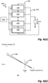
- the outputs from AVP converter-module control and power units 430 are connected in parallel at 450, and the currents are balanced using a circular chain, or daisy-chain, communication 460, such that each element balances the current with the average of its neighbours' current.
- This approach has two strengths: firstly it cancels out voltage offsets and droop mismatches, secondly it is fault tolerant on the current sharing - since there is no single wire, a fault on the inter-module communication 460 can be detected and isolated. However, it relies on a single voltage reference 420 that is shared with all modules, so it does not achieve high accuracy and fault tolerance on the reference.
- the voltage-current characteristic of the modules are shown in figure 4(b) .
- the modules can be controlled to each provide the same current Iload/n, at the operating voltage V out , as seen at 470. It is noted that one of the modules acts as master, with its V-I characteristic 480, and thus this approach is not entirely fault-tolerant.
- embodiments of the present disclosure may provide for truly distributed control, with fault tolerance, and the potential for high accuracy.
- figure 5 shows an arrangement 500 of multiple regulator modules 510 connected in parallel, each with a local voltage reference 520 and control and power unit 530, and current sharing, or daisy-chain, communication 560.
- the control and power unit may be subdivided, as shown, into a control unit 532, which controls the voltage regulation, and a power unit 534, which regulates the voltage.
- the power unit 534 may include a power-dissipating impedance
- the power unit may includes one or more switches and an impedance.
- each of the regulator modules 510 may be identical, and there is no artificial limit to the number which may be combined.
- the output from the modules are connected in parallel.
- Each module regulates independently its the output voltage, using its own reference voltage 520.
- Each module has a non-null virtual output impedance R out , to facilitate voltage droop, or AVP, regulation as discussed above.
- a common output voltage value V out is proportional to the average of the voltage references. The averaging occurs automatically at the output without a need for added communication between the modules, as will be explained in more detail below. Using an average of several voltage references may yield an accuracy that is improved compared to the accuracy of one module; this benefit may further increase with an increasing number of modules.
- a current sharing loop 560 is based on local current sensing 565 of the current output from each module, and typically provides communication of current values between neighbouring modules along a circular chain, or daisy-chain.
- An finite DC loop gain H but having an infinite output resistance R out such that H*R out is infinite, is further used to reduce differential currents while preserving the output voltage accuracy. That is to say, in steady state (or "DC") the control loops force the output currents to be the same.
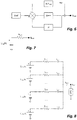
- FIG. 6 shows, schematically, the main control loop, in DC operation, of a module according to one or more embodiments.
- Each module comprises a voltage reference V ref , and a regulation loop with non-null output impedance.
- V ref voltage reference
- R out regulation loop with non-null output impedance.
- the output impedance R out is determined by a current loop with local current sensing of the output current.
- the loop gain G shows a high DC gain - typically greater than 1000; which is effectively an infinite DC gain.
- the output reference is proportional to the average of the local references and the output droop is also proportional to the average of the local droops.
- Equation (16) below describes the differential current attached to module "k" as a function of small shifts observed in the reference voltage value, feedback gain value and output impedance value. Differential currents are limited because the output impedance is not null. Equation (18) below shows that the bigger the output resistance is, the lower are the differential currents. However, a circuit for reducing the differential currents may be desirable, especially if choosing an output impedance of high value is not possible for the application.
- I out k ⁇ I load n ⁇ ⁇ V ref ⁇ ⁇ H ⁇ ⁇ V out ⁇ R out ⁇ + ⁇ V ref ⁇ ⁇ H ⁇ . ⁇ R out ⁇ . 1 + ⁇ vref k 1 + ⁇ h k . 1 + ⁇ rout k ⁇ V out ⁇ R out ⁇ . 1 1 + ⁇ rout k ⁇ I load n
- Equation (18) can be rewritten as: I out k ⁇ I load n ⁇ ⁇ h k ⁇ ⁇ vref k . ⁇ V ref ⁇ + ⁇ out k V ref ⁇ ⁇ V ref ⁇ ⁇ V out ⁇ H ⁇ . ⁇ R out ⁇
- the droop may be as little as one tenth, or less, of Vref. So it is in general preferable to match Vref to reduce, ⁇ vref k
- a current sharing - or current matching - circuit is implemented, to reduce differential currents.
- the current sharing circuit corrects the local reference voltage from sensing the local output current and comparing it with currents from other modules.
- the most convenient approach is to compare with the two immediately neighbouring modules, typically using bi-directional communication around a daisy-chain or circular chain). However, it is possible to compare with just a single neighbour (for instance, using uni-directional communication around the daisy-chain), or with additional, more remote, modules.
- the k-th module receives current sense information from modules (k-1) and (k+1), whilst in the unidirectional communication, the k-th module receives current sense information from only the (k-1)th module.
- the average of those currents are typically used for the comparison: (I k+1 +I k-1 )/2, as shown in figure 9 . Conversely, in embodiments where the comparison is with just one neighbour, that neighbour's current is used directly (I k-1 ).
- a weighted average may be used: w 1 . I 1 + w 2 . I 2 + ⁇ + w k ⁇ 1 . I k ⁇ 1 + w k + 1 .
- FIG. 9 shows, schematically, the control of a "k-th" voltage regulator module, according to embodiments of the present disclosure.
- the primary control loop 910 implements AVP or voltage droop regulation as discussed above. However, instead of controlling directly from the reference voltage V refk , the control is carried out based on an adjusted reference voltage V refk '.
- the adjusted reference voltage is determined by the current sharing, or current balancing, loop, 920. As shown, the current balancing loop uses the difference between the output current I outk from the local voltage regulator, and an average current from other voltage regulator modules in the multi-module voltage regulator - in this example, the mean of the currents I outk+1 and I outk-1 , from the two neighbouring modules.
- Proportional correction (finite DC gain) is applied in this current sharing loop.
- V out ⁇ V ref ⁇ ⁇ H ⁇ ⁇ ⁇ R out ⁇ n .
- Equation (21) and (23) lead to: I out k ⁇ I load n ⁇ ⁇ h k + ⁇ rout k ⁇ ⁇ vref k . ⁇ V ref ⁇ ⁇ ⁇ rout k . ⁇ H ⁇ . V out ⁇ H ⁇ . ⁇ R out ⁇ + R diff
- Equation (27), compared with equation (18), shows that the introduction of the current sharing operation can reduce differential currents as if an additional output impedance Rdiff was added in the modules, while common mode operation is not affected (equation (23)).
- embodiments according to the present disclosure may result in improved output voltage accuracy based on multiple reference voltages, reduced differential currents, and complete modular decentralized control with inter-module communication - typically along a daisy-chain or circular chain.
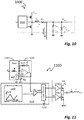
- FIG. 10 shows, as a non-limiting example, one such voltage regulator.
- the figure shows a switched mode buck converter 1000, having a half-bridge node SW which is switched between a supply voltage Vin and ground, by PWM controller 1110, to switchedly supply current through an inductor Lf, to an output by a filter Rdcr,Resr,Cout, where Rdcr is the parasitic resistance of the inductor Lf, and Resr if the parasitic resistance of the capacitor Cout
- the current through the inductor provides an output voltage Vout, and is sensed (Isense),.
- FIG 11 depicts a buck 1100 converter, the half-bridge switches of which are driven by high and low-side drivers Driver_HS, and Driver_LS.
- the drivers are controlled by logic control 1110.
- the logic takes input from an oscillator 1140.
- G infinite gain
Landscapes
- Engineering & Computer Science (AREA)
- Power Engineering (AREA)
- Physics & Mathematics (AREA)
- Electromagnetism (AREA)
- General Physics & Mathematics (AREA)
- Radar, Positioning & Navigation (AREA)
- Automation & Control Theory (AREA)
- Dc-Dc Converters (AREA)
- Continuous-Control Power Sources That Use Transistors (AREA)
Abstract
Description
- This disclosure relates to multi-module voltage regulators, and voltage regulator modules and control modules therefor.
- Voltage regulators (VRs) supply a regulated voltage to other circuits or systems. A voltage regulator can be linear (linear regulator, LDO) or a switching mode power supply SMPS (DCDC converters, charge pumps).
- The accuracy of the regulated voltage accuracy is directly proportional to the voltage reference. When the output current required is high, multiple converter legs, or modules, can be connected in parallel, as illustrated schematically in
figure 1 , which shows a multi-modulevoltage regulator system 100 havingseveral regulator modules 110 each driven by the same control voltage supplied to a control input cntl. The outputs of the modules are combined to provide a current I to aload 120, at a voltage Vout. The voltage Vout is provided to each module through a feedback loop. - This multi-module approach may provide for advantages such as scalability, improved thermal spreading, reduced electromagnetic interference (EMI), reduced filtering requirements, better transient response, and possible safety or fault tolerance mechanisms when a failing leg or module is identified and disabled. Conventional control methods use a centralized controller, either a separate unit, or in a mater/slave arrangement in which one of the modules is configured a master and has associated with it, the controller. The centralized controller or master provides a control voltage for the regulation operation. But this controller is a single point-of-failure, so typically the complete system fails if there is a failure in the controller.
- Recently, methods have been proposed for decentralised, or distributed, control, which can improve the fault tolerance of the regulator. However, there remain a problem for improved accuracy of such voltage regulators.
- According to a first aspect of the present disclosure there is provided controller for a voltage regulator module including a power unit and providing, at an output, an output current, lout, at an output voltage, Vout, from an input current at an input voltage, the voltage regulator module being configured for use in a multi-module voltage regulator having at least one neighbouring voltage regulator module having a respective output in connected in parallel with the output, the controller comprising: a reference voltage source for providing a reference voltage (Vref); a current balancing unit, configured to receive a respective output current from each of the at least one neighbouring voltage regulator module and to determine an adjusted reference voltage, Vref', from the reference voltage and for balancing the output current with the at least one respective output current; and a control unit configured to use the adjusted reference voltage to control the voltage regulator module, to provide the output current at the output voltage from the input current at the input voltage, based on adaptive voltage positioning, AVP, regulation.
- In one or more embodiments, the current balancing module is configured to determine a difference, the difference being a difference between the output current and the output current from a one neighbouring voltage regulator module, and to adjust the reference voltage in proportion to the difference to provide the adjusted reference voltage. The communication of the output current from the neighbouring voltage regulator module may be provided by a uni-directional link, or may be provided by a bi-directional link in the case that communication in one direction fails.
- In other embodiments, the current balancing module is configured to determine a difference, the difference being a difference between the output current and the sum of half the output currents from each of two neighbouring voltage regulator modules, and to adjust the reference voltage in proportion to the difference to provide the adjusted reference voltage. The modules may typically be arranged in a daisy-chain, and then there is thus a communication path between the two direct neighbours of the voltage regulator module, and the module. This may typically be provided by bi-directional links.
- In yet other embodiments, the current balancing module is configured to determine a difference, the difference being a difference between the output current and a weighted average of the output currents from a plurality of neighbouring voltage regulator modules, and to adjust the reference voltage in proportion to the difference to provide the adjusted reference voltage
- In one or more embodiments, wherein the control unit (532) is configured to control the voltage regulator module to provide the output current from the input current, and the adjusted reference voltage by a control loop having a finite feedback gain, H. This may be useful to achieve the correct output voltage in cases where the reference voltage is fixed or in which the output voltage is higher than the supply of the control module.
- In one or more embodiments, the current balancing unit (550) is configured to adjust the reference voltage by the difference multiplied by a finite loop gain value, H,Rdiff to determine the adjusted reference voltage. Implementation of finite gain may assist in preventing, in operation, one controller from asserting a current on all the other controllers in the multi-module voltage regulator
- In one or more embodiments the control loop of the control unit has an infinite DC gain. Providing an infinite DC gain may be useful to ensure accurate or precise AVP regulation in steady-state situations: otherwise steady-state error may provide an offset - typically fixed - for the output voltage Vout.
- In one or more embodiments the output voltage is determined, by voltage droop regulation, as the difference between the adjusted reference voltage divided by the feedback gain, and the output current multiplied by an output impedance, Rout:

- In one or more embodiments the controller is adapted for use in a multi-module voltage regulator comprising at least three voltage regulator modules operable with distributed control whose controllers are arranged in a logical daisy-chain, wherein the reference voltage source, the output current, the common output voltage and the respective output currents from the two immediately neighbouring voltage regulator modules in the daisy-chain are the only control inputs for controlling the output current. This may simplify the design, and may enhance the modularity of the controller.
- In one or more embodiments the current balancing module is further configured to detect a failure of communication from a one of the two neighbouring voltage regulator modules, and in response to the failure of communication determine the difference to be a difference between the output current and the output current from the other of the two neighbouring voltage regulator modules,
- According to a second aspect of the present disclosure, there is provided a voltage regulator module comprising a controller described above and further comprising a power unit having at least one controllable switch and an impedance. The power unit may integral with the control unit, or may be separate, in the sense of being on a separate chip of in a separate package, therefrom. According to a third aspect of the present disclosure, there is provided a multi-module voltage regulator, comprising at least two such voltage regulator modules, having respective controllers arranged in a logical daisy-chain, wherein the respective controller of each voltage regulator modules includes a separate reference voltage source, and the output voltage of the regulator modules is common. The at least one neighbouring voltage regulator module may be supplied from the same input voltage as the voltage regulator module. Conversely, in one of more other embodiments, the or each of the at least one neighbouring voltage regulator module may be supplied from one or more different input voltages. This may improve availability.
- According to a fourth aspect of the present disclosure, there is provided a method of providing distributed control of a multi-module voltage regulator providing a common output voltage and comprising at least two voltage regulator modules and each having a respective controller, the controllers being arranged in a logical daisy-chain, the method comprising, in each voltage regulator module: providing a reference voltage by means of a reference voltage source; adjusting the reference voltage in dependence on a difference between an output current of the voltage regulator module and a weighted average of the respective output currents from at least one other voltage regulator module comprised in the multi-module voltage regulator by a finite gain feedback loop; and controlling the output current and the common output voltage from the adjusted reference voltage, by AVP regulation.
- The weighted average may be the sum of half the output currents from each of two neighbouring voltage regulator modules.
- There may be provided a computer program, which when run on a computer, causes the computer to configure any apparatus, including a circuit, controller, sensor, filter, or device disclosed herein or perform any method disclosed herein. The computer program may be a software implementation, and the computer may be considered as any appropriate hardware, including a digital signal processor, a microcontroller, and an implementation in read only memory (ROM), erasable programmable read only memory (EPROM) or electronically erasable programmable read only memory (EEPROM), as non-limiting examples. The software implementation may be an assembly program.
- The computer program may be provided on a computer-readable medium, which may be a physical computer-readable medium, such as a disc or a memory device, or may be embodied as another non-transient signal.
- These and other aspects of the invention will be apparent from, and elucidated with reference to, the embodiments described hereinafter.
- Embodiments will be described, by way of example only, with reference to the drawings, in which
-
figure 1 shows, in schematic form, an arrangement of multiple regulators connected in parallel. -
figure 2 illustrates a voltage-current characteristic showing the concept of voltage droop; -
figure 3(a) shows an arrangement of multiple regulators connected in parallel with shared wired voltage references -
figure 3(b) illustrates the voltage-current characteristic of the modules offigure 3(a) ; -
figure 4(a) shows an arrangement of multiple regulators connected in parallel with daisy-chain current communication; -
figure 4(b) illustrates the voltage-current characteristic of the modules offigure 4(a) ; -
figure 5 shows an arrangement of multiple regulators connected in parallel with local voltage references and current sharing communication according to one or more embodiments; -
figure 6 shows, schematically, the DC operation of a module according to one or more embodiments; -
figure 7 shows a DC model of a single module; -
figure 8 shows a DC model of n modules connected in parallel; -
figure 9 shows the control scheme of a controller according to embodiments; -
figure 10 shows a switched mode buck converter; and -
figure 11 shows a switched mode buck converter operating under AVP. - It should be noted that the Figures are diagrammatic and not drawn to scale. Relative dimensions and proportions of parts of these Figures have been shown exaggerated or reduced in size, for the sake of clarity and convenience in the drawings. The same reference signs are generally used to refer to corresponding or similar features in modified and different embodiments.
- An idealised voltage regulator may operate as a perfect voltage source - that is to say, the output voltage remains constant irrespective of the current supplied. However, the outputs of two such regulators could not be connected in parallel, since this would result in very high - theoretically infinite - currents flowing between the two, to try to offset any, even very small, differences in output voltage.
- To enable two or more such regulator modules to be connected in parallel (or be "parallelized"), they must not be operated as ideal voltage sources. Instead, the concept of "voltage droop" is utilised. This is illustrated in
figure 2 . The regulator is designed to have a "virtual output impedance" Rout, such that the output voltage Vout decreases, or "droops", from an initial value Vout0, with increasing load current Iload up to a maximum allowed load current Iloadmax :
- The control of such voltage regulators may be described as being by "voltage droop regulation", which is also referred to as Adaptive Voltage Positioning (AVP) regulation. AVP allows parallel connection with well-controlled differential currents flowing from one module to another due to internal offsets or mismatches. AVP naturally provides some degree of current sharing and better transient response as well as improved system power efficiency, so that it is presently used in CPU/GPU (central processor unit / general processor unit) power supplies.
- As will be discussed in more detail below, AVP regulation with multiple modules can be implemented with each module having its own reference voltage. The output voltage is then proportional to the average of the reference voltages. However, parallelizing with AVP typically provides only a poor level of current sharing. Current imbalance is given by mismatches from the reference voltages and the output droops (i.e. virtual output impedance). Therefore, some communication links are required to improve the current sharing. That is why distributed, or decentralized, controllers are typically configured to be modular with standard connections - which allows the use of an unlimited number of elements.
- Methods of improving the current sharing for multi-module VRs are known. One such method is averaging the reference voltage in a shared wire, as shown in Error! Reference source not found.. This figure shows a multi-module voltage regulator, having
several regulator modules 310, each of which includes its own localvoltage reference Vref 320 in addition to a control andpower unit 330. The power andcontrol unit 330 may have separate control unit 332 and power unit 334 as shown. The local voltage references are tied together by a sharedwire 340. - Such an approach cancels out differential currents, at the nominated output current Iout0, due to voltage reference mismatch, as shown in
figure 3b , by the imposition of a common value of Vref; however, mismatches in the virtual output impendences of the modules, combined with droop mismatch, result in the modules providing a range of current outputs Ioutk, from each of the modules at a different operational voltage Vout. - Shared wire approaches are in general not fault tolerant, since the shared wire is a single-point-of-failure, and such approaches still have poor current sharing because of the mismatches in the output currents resulting from the differences between each converter's output impedance. Further, although a single wire could be added for current balancing, this would also be a single point of failure (SPO F) and thus not fault-tolerant.
- An alternative approach has been proposed by one of the present inventors (Cousineau, Marc, and Zijian Xiao. "Fully Decentralized Modular Approach for Parallel Converter Control." In Applied Power Electronics Conference and Exposition (APEC), 2013 Twenty-Eighth Annual IEEE, 237-243. IEEE, 2013). This is illustrated in
figure 4(a) . - In this approach, the outputs from AVP converter-module control and
power units 430 are connected in parallel at 450, and the currents are balanced using a circular chain, or daisy-chain,communication 460, such that each element balances the current with the average of its neighbours' current. This approach has two strengths: firstly it cancels out voltage offsets and droop mismatches, secondly it is fault tolerant on the current sharing - since there is no single wire, a fault on theinter-module communication 460 can be detected and isolated. However, it relies on asingle voltage reference 420 that is shared with all modules, so it does not achieve high accuracy and fault tolerance on the reference. - The voltage-current characteristic of the modules are shown in
figure 4(b) . In this approach, the modules can be controlled to each provide the same current Iload/n, at the operating voltage Vout, as seen at 470. It is noted that one of the modules acts as master, with its V-I characteristic 480, and thus this approach is not entirely fault-tolerant. - In contrast to the known approaches, embodiments of the present disclosure may provide for truly distributed control, with fault tolerance, and the potential for high accuracy. Once such embodiment is shown in
figure 5 , which shows an arrangement 500 ofmultiple regulator modules 510 connected in parallel, each with alocal voltage reference 520 and control andpower unit 530, and current sharing, or daisy-chain,communication 560. The control and power unit may be subdivided, as shown, into acontrol unit 532, which controls the voltage regulation, and apower unit 534, which regulates the voltage. As non-limiting examples, in a linear regulator thepower unit 534 may include a power-dissipating impedance, whereas in a switched mode power converter the power unit may includes one or more switches and an impedance. - In this arrangement, each of the
regulator modules 510 may be identical, and there is no artificial limit to the number which may be combined. The output from the modules are connected in parallel. Each module regulates independently its the output voltage, using itsown reference voltage 520. Each module has a non-null virtual output impedance Rout, to facilitate voltage droop, or AVP, regulation as discussed above. A common output voltage value Vout is proportional to the average of the voltage references. The averaging occurs automatically at the output without a need for added communication between the modules, as will be explained in more detail below. Using an average of several voltage references may yield an accuracy that is improved compared to the accuracy of one module; this benefit may further increase with an increasing number of modules. Acurrent sharing loop 560 is based on local current sensing 565 of the current output from each module, and typically provides communication of current values between neighbouring modules along a circular chain, or daisy-chain. An finite DC loop gain H, but having an infinite output resistance Rout such that H*Rout is infinite, is further used to reduce differential currents while preserving the output voltage accuracy. That is to say, in steady state (or "DC") the control loops force the output currents to be the same. - The control will now be explained, with reference to
figures 6 to 9 . -
Figure 6 shows, schematically, the main control loop, in DC operation, of a module according to one or more embodiments. Each module comprises a voltage reference Vref, and a regulation loop with non-null output impedance. Various forms of voltage reference, such as a band-gap reference, will be known to the skilled person. The output impedance Rout is determined by a current loop with local current sensing of the output current. The loop gain G shows a high DC gain - typically greater than 1000; which is effectively an infinite DC gain. Feedback gain H defines the ratio between the reference voltage Vref and the output voltage Vout. Then:
- The DC operation of a single module can be simplified and modelized with a voltage source Vref/H, followed by an output impedance, as illustrated in
Figure 7 . An arrangement of "n" modules gives the association of "n" voltage sources connected together to the output node through their output impedance, as illustrated infigure 8 , where, "n" is an integer greater or equal to two. - The following relationships can then be seen:
For all of the local references, Vrefk, k=1 to n, the following holds:

- The output impedances of the modules are, similarly:


- Moreover, the local feedback gains can be shown to be:


- And finally, the local output currents are:


- From the above, it can be shown that the output voltage Vout is proportional to the average of the voltage references:


- In other words, the output reference is proportional to the average of the local references and the output droop is also proportional to the average of the local droops.
- Potential mismatches between modules (voltage references Vref, feedback ratio H, output impedance Rout) generate undesirable differential currents (current flowing from a module to another, and thus not transferred to the load). Equation (16) below describes the differential current attached to module "k" as a function of small shifts observed in the reference voltage value, feedback gain value and output impedance value. Differential currents are limited because the output impedance is not null. Equation (18) below shows that the bigger the output resistance is, the lower are the differential currents. However, a circuit for reducing the differential currents may be desirable, especially if choosing an output impedance of high value is not possible for the application.
- Differential current in one module can be described through:


- Using a first order approximation gives:

- From (15) to (17), it follows that

- Equation (18) can be rewritten as:

- This shows that the impact of εvref
k the current error is much higher than the impact of εroutk because 〈Vref〉 tends to be 10 times bigger than the droop at full load: [〈Vref〉 - 〈H〉.Vout]. - Typically, the droop may be as little as one tenth, or less, of Vref. So it is in general preferable to match Vref to reduce, εvref
k - According to embodiments of the present disclosure, a current sharing - or current matching - circuit is implemented, to reduce differential currents. The current sharing circuit corrects the local reference voltage from sensing the local output current and comparing it with currents from other modules. The most convenient approach is to compare with the two immediately neighbouring modules, typically using bi-directional communication around a daisy-chain or circular chain). However, it is possible to compare with just a single neighbour (for instance, using uni-directional communication around the daisy-chain), or with additional, more remote, modules. An example of the latter would be a "leap-frog" communication chain in which each module would communicate with its immediate next-neighbours and its next-but-one neighbours, such that a k-th module communicates with, or more particularly receives current sense information from, modules (k-2), (k-1), (k+1) and (k=2). Conversely, in the bi-direction immediate neighbour arrangement, the k-th module receives current sense information from modules (k-1) and (k+1), whilst in the unidirectional communication, the k-th module receives current sense information from only the (k-1)th module.
- In embodiments in which the local output current is compared with the currents from with the two neighbouring modules, the average of those currents are typically used for the comparison: (Ik+1+Ik-1)/2, as shown in
figure 9 . Conversely, in embodiments where the comparison is with just one neighbour, that neighbour's current is used directly (Ik-1). In general, a weighted average may be used:
-
Figure 9 shows, schematically, the control of a "k-th" voltage regulator module, according to embodiments of the present disclosure. Theprimary control loop 910 implements AVP or voltage droop regulation as discussed above. However, instead of controlling directly from the reference voltage Vrefk, the control is carried out based on an adjusted reference voltage Vrefk'. The adjusted reference voltage is determined by the current sharing, or current balancing, loop, 920. As shown, the current balancing loop uses the difference between the output current Ioutk from the local voltage regulator, and an average current from other voltage regulator modules in the multi-module voltage regulator - in this example, the mean of the currents Ioutk+1 and Ioutk-1, from the two neighbouring modules. - Proportional correction (finite DC gain) is applied in this current sharing loop.
- The use of a finite DC gain (that is to say, as measured in Ohms, Hk.Rdiff ≠ avoids impacting the main voltage loop accuracy: otherwise, one of the modules might go into saturation under this loop operation, and it could impose its current as a new reference for all the modules currents. That would result in a shifting of the sum of the output currents, so the output voltage would be offset from the average of the references, which would generally not be desirable.
- With a finite DC gain in the current sharing loop, correction of the differential currents does not affect the accuracy of the output voltage, because the sum of the corrections from sharing operations is null as showed by equations (20) to (27) below.
- It follows from the circular-chained property, that (eq19):

- And using a first order approximation, this results in:

- Calculation of the output voltage with the current sharing loop:


- From (20) and (22) one gets:

- Calculation of the differential current with the correction:


- Equation (21) and (23) lead to:

- Equation (27), compared with equation (18), shows that the introduction of the current sharing operation can reduce differential currents as if an additional output impedance Rdiff was added in the modules, while common mode operation is not affected (equation (23)).
- It can thus be seen that embodiments according to the present disclosure may result in improved output voltage accuracy based on multiple reference voltages, reduced differential currents, and complete modular decentralized control with inter-module communication - typically along a daisy-chain or circular chain.
- The control methods and apparatus disclosed herein may be used with linear regulators, or switched mode regulators.
Figure 10 shows, as a non-limiting example, one such voltage regulator. The figure shows a switchedmode buck converter 1000, having a half-bridge node SW which is switched between a supply voltage Vin and ground, byPWM controller 1110, to switchedly supply current through an inductor Lf, to an output by a filter Rdcr,Resr,Cout, where Rdcr is the parasitic resistance of the inductor Lf, and Resr if the parasitic resistance of the capacitor Cout The current through the inductor provides an output voltage Vout, and is sensed (Isense),. - Control of such a VR, by AVP or voltage droop regulation, is illustrated in
figure 11. Figure 11 depicts abuck 1100 converter, the half-bridge switches of which are driven by high and low-side drivers Driver_HS, and Driver_LS. The drivers are controlled bylogic control 1110. The logic takes input from anoscillator 1140. An infinite gain (G=∞)DC control loop 1120 is provided with afeedback loop 1130, based on the output impedance Rout, to control the PWM signal in dependence on the output current li . The other details of such a buck converter will be familiar to the skilled person. - From reading the present disclosure, other variations and modifications will be apparent to the skilled person. Such variations and modifications may involve equivalent and other features which are already known in the art of voltage regulators, and which may be used instead of, or in addition to, features already described herein.
- Although the appended claims are directed to particular combinations of features, it should be understood that the scope of the disclosure of the present invention also includes any novel feature or any novel combination of features disclosed herein either explicitly or implicitly or any generalisation thereof, whether or not it relates to the same invention as presently claimed in any claim and whether or not it mitigates any or all of the same technical problems as does the present invention.
- Features which are described in the context of separate embodiments may also be provided in combination in a single embodiment. Conversely, various features which are, for brevity, described in the context of a single embodiment, may also be provided separately or in any suitable sub-combination. The applicant hereby gives notice that new claims may be formulated to such features and/or combinations of such features during the prosecution of the present application or of any further application derived therefrom.
- For the sake of completeness it is also stated that the term "comprising" does not exclude other elements or steps, the term "a" or "an" does not exclude a plurality, a single processor or other unit may fulfil the functions of several means recited in the claims and reference signs in the claims shall not be construed as limiting the scope of the claims.
-
- 100,300, 400
- multi-module voltage regulator
- 110
- regulator module
- 120
- load
- 310
- regulator module with local reference voltage
- 320
- local voltage reference
- 330
- control and power unit
- 332
- control unit
- 334
- power unit
- 340
- shared wired
- 420
- single voltage reference
- 430
- AVP converter module control and power unit
- 460
- parallel connection between control and power unit outputs
- 460
- daisy-chain communication
- 470
- operating point Vout with current Iload/n
- 480
- master module V-I characteristic
- 500
- arrangement of multiple regulator modules
- 510
- regulator module
- 515
- controller
- 520
- local voltage reference
- 530
- control and power unit
- 532
- control unit
- 534
- power unit
- 550
- current balancing unit
- 560
- current sharing, or daisy-chain communication
- 565
- local current sensing
- 1000
- buck converter
- 1010
- PWM controller
- 1100
- buck converter with AVP regulation
- 1110
- logic control
- 1120
- Infinite DC gain
- 1130
- feedback loop based in output impedance
- 1140
- oscillator
Claims (15)
- A controller (515),
for a voltage regulator module (510) including a power unit (534) and providing, at an output, an output current, lout, at an output voltage, Vout, from an input current at an input voltage, the voltage regulator module being configured for use in a multi-module voltage regulator (500) having at least one neighbouring voltage regulator module having a respective output connected in parallel with the output,
the controller comprising:a reference voltage source (520) for providing a reference voltage (Vref); a current balancing unit (550), configured to receive a respective output current from each of the at least one neighbouring voltage regulator module and to determine an adjusted reference voltage, Vref', from the reference voltage and for balancing the output current with the at least one respective output current; anda control unit (532) configured to use the adjusted reference voltage to control the voltage regulator module, to provide the output current at the output voltage from the input current at the input voltage, based on adaptive voltage positioning, AVP, regulation. - A controller as claimed in claim 1, wherein the current balancing module is configured to determine a difference, the difference being a difference between the output current and the output current from a one neighbouring voltage regulator module, and to adjust the reference voltage in proportion to the difference to provide the adjusted reference voltage.
- A controller as claimed in claim 1, wherein the current balancing module is configured to determine a difference, the difference being a difference between the output current and the sum of half the output currents from each of two neighbouring voltage regulator modules, and to adjust the reference voltage in proportion to the difference to provide the adjusted reference voltage.
- A controller as claimed in claim 1, wherein the current balancing module is configured to determine a difference, the difference being a difference between the output current and a weighted average of the output currents from a plurality of neighbouring voltage regulator modules, and to adjust the reference voltage in proportion to the difference to provide the adjusted reference voltage.
- A controller as claimed in any proceeding claim wherein the control unit (532) is configured to control the voltage regulator module to provide the output current from the input current, and the adjusted reference voltage by a control loop having a finite feedback gain, H.
- A controller as claimed in any of claims 2 to 4, wherein the current balancing unit (550) is configured to adjust the reference voltage by the difference multiplied by a finite loop gain value, H,Rdiff to determine the adjusted reference voltage.
- A controller as claimed in claim 5 wherein the control loop of the control unit has an infinite DC gain.
- A controller as claimed in any of claims 6 to 8, wherein the output voltage is determined, by voltage droop regulation, as the difference between the adjusted reference voltage divided by the feedback gain, and the output current multiplied by an output impedance, Rout:

- A controller as claimed in any previous claim and adapted for use in a multi-module voltage regulator comprising at least three voltage regulator modules operable with distributed control whose controllers are arranged in a logical daisy-chain, wherein the reference voltage source, the output current, the common output voltage and the respective output currents from the two immediately neighbouring voltage regulator modules in the daisy-chain are the only control inputs for controlling the output current.
- A controller as claimed any claim 3 or any of claims 4 to 9 when dependant on claim 3, wherein the current balancing module is further configured to detect a failure of communication from a one of the two neighbouring voltage regulator modules, and in response to the failure of communication determine the difference to be a difference between the output current and the output current from the other of the two neighbouring voltage regulator modules,
- A voltage regulator module comprising a controller as claimed in any preceding claim, and further comprising a power unit having at least one controllable switch and an impedance.
- A multi-module voltage regulator, comprising at least two voltage regulator modules as claim in claim 11 , having respective controllers arranged in a logical daisy-chain, wherein the respective controller of each voltage regulator modules includes a separate reference voltage source, and the output voltage of the regulator modules is common.
- A multi-module voltage regulator as claimed in claim 12, wherein the at least one neighbouring voltage regulator module is supplied from the input voltage.
- A method of providing distributed control of a multi-module voltage regulator providing a common output voltage and comprising at least two voltage regulator modules and each having a respective controller, the controllers being arranged in a logical daisy-chain, the method comprising, in each voltage regulator module:providing a reference voltage by means of a reference voltage source;adjusting the reference voltage in dependence on a difference between an output current of the voltage regulator module and a weighted average of the respective output currents from at least one other voltage regulator module comprised in the multi-module voltage regulator by a finite gain feedback loop; andcontrolling the output current and the common output voltage from the adjusted reference voltage, by AVP regulation.
- The method of claim 14 wherein adjusting the reference voltage the weighted average is the sum of half the output currents from each of two neighbouring voltage regulator modules.
Priority Applications (3)
| Application Number | Priority Date | Filing Date | Title |
|---|---|---|---|
| EP19306578.6A EP3832429B1 (en) | 2019-12-05 | 2019-12-05 | Distributed control of a voltage regulator |
| US17/109,977 US11456671B2 (en) | 2019-12-05 | 2020-12-02 | Distributed control of a voltage regulator |
| CN202011413859.7A CN112925372B (en) | 2019-12-05 | 2020-12-04 | Distributed control of voltage regulators |
Applications Claiming Priority (1)
| Application Number | Priority Date | Filing Date | Title |
|---|---|---|---|
| EP19306578.6A EP3832429B1 (en) | 2019-12-05 | 2019-12-05 | Distributed control of a voltage regulator |
Publications (2)
| Publication Number | Publication Date |
|---|---|
| EP3832429A1 true EP3832429A1 (en) | 2021-06-09 |
| EP3832429B1 EP3832429B1 (en) | 2023-02-08 |
Family
ID=69005649
Family Applications (1)
| Application Number | Title | Priority Date | Filing Date |
|---|---|---|---|
| EP19306578.6A Active EP3832429B1 (en) | 2019-12-05 | 2019-12-05 | Distributed control of a voltage regulator |
Country Status (3)
| Country | Link |
|---|---|
| US (1) | US11456671B2 (en) |
| EP (1) | EP3832429B1 (en) |
| CN (1) | CN112925372B (en) |
Families Citing this family (5)
| Publication number | Priority date | Publication date | Assignee | Title |
|---|---|---|---|---|
| KR20230045933A (en) * | 2021-09-29 | 2023-04-05 | 에스케이하이닉스 주식회사 | Storage device based on daisy chain topology |
| US12093068B2 (en) | 2022-06-14 | 2024-09-17 | Apple Inc. | Scalable low dropout regulator having multiple pass circuits |
| US11928000B1 (en) * | 2022-08-25 | 2024-03-12 | Dell Products L.P. | Calibrating processor system power consumption |
| CN116154749B (en) * | 2023-01-06 | 2025-11-11 | 西北工业大学 | Layering control method for high average peak ratio hybrid energy system of multi-motor aircraft |
| CN119717981B (en) * | 2024-12-20 | 2025-09-16 | 西安交通大学 | A linear voltage regulator and loop weight adjustment method thereof |
Family Cites Families (15)
| Publication number | Priority date | Publication date | Assignee | Title |
|---|---|---|---|---|
| US6215290B1 (en) * | 1999-11-15 | 2001-04-10 | Semtech Corporation | Multi-phase and multi-module power supplies with balanced current between phases and modules |
| US7274114B1 (en) * | 2004-11-15 | 2007-09-25 | National Semiconductor Corporation | Integrated tracking voltage regulation and control for PMUIC to prevent latch-up or excessive leakage current |
| US8441241B2 (en) * | 2010-05-03 | 2013-05-14 | Intel Corporation | Methods and systems to digitally balance currents of a multi-phase voltage regulator |
| US8841893B2 (en) * | 2010-12-16 | 2014-09-23 | International Business Machines Corporation | Dual-loop voltage regulator architecture with high DC accuracy and fast response time |
| US8669674B2 (en) * | 2010-12-17 | 2014-03-11 | Nxp B.V. | Power supply circuit with shared functionality and method for operating the power supply circuit |
| FR2993112B1 (en) | 2012-07-04 | 2014-08-15 | Toulouse Inst Nat Polytech | STATIC-BASED PARALLEL OR SERIAL AND DECENTRALIZED MODULAR CONTROL (CDM) STATIC CONVERTERS |
| US9461539B2 (en) * | 2013-03-15 | 2016-10-04 | Taiwan Semiconductor Manufacturing Company, Ltd. | Self-calibrated voltage regulator |
| US9401640B2 (en) | 2013-04-11 | 2016-07-26 | Telefonaktiebolaget L M Ericsson (Publ) | Voltage droop control in a voltage-regulated switched mode power supply |
| US10530303B2 (en) | 2016-05-25 | 2020-01-07 | Cirrus Logic, Inc. | Multi-phase power converter system using multiple amplifier integrated circuits |
| US10131245B2 (en) * | 2016-08-16 | 2018-11-20 | Ford Global Technologies, Llc | Electrified vehicle DC power conversion with distributed control |
| US10320296B2 (en) * | 2017-09-27 | 2019-06-11 | Taiwan Semiconductor Manufacturing Co., Ltd. | Multi-phase voltage regulator system |
| US10432088B1 (en) * | 2018-06-05 | 2019-10-01 | Dialog Semiconductor (Uk) Limited | Two-stage multi-phase switching power supply with cross-domain adaptive voltage and frequency regulation |
| KR102611984B1 (en) * | 2018-10-10 | 2023-12-08 | 삼성전자주식회사 | Multi-phase switching regulator comprising interleaving circuit and swithcing regulating method using thereof |
| CN110445381B (en) * | 2019-07-26 | 2021-07-16 | 成都芯源系统有限公司 | Multiphase switch converter containing daisy chain structure and phase switching control method thereof |
| CN115542996B (en) * | 2022-11-28 | 2023-03-24 | 中晟微电子(南京)有限公司 | A low-dropout linear regulator with high power supply rejection ratio and its control method |
-
2019
- 2019-12-05 EP EP19306578.6A patent/EP3832429B1/en active Active
-
2020
- 2020-12-02 US US17/109,977 patent/US11456671B2/en active Active
- 2020-12-04 CN CN202011413859.7A patent/CN112925372B/en active Active
Non-Patent Citations (6)
| Title |
|---|
| CINGOZ FATIH ET AL: "Optimized Settings of Droop Parameters Using Stochastic Load Modeling for Effective DC Microgrids Operation", IEEE TRANSACTIONS ON INDUSTRY APPLICATIONS, IEEE SERVICE CENTER, PISCATAWAY, NJ, US, vol. 53, no. 2, 1 March 2017 (2017-03-01), pages 1358 - 1371, XP011642991, ISSN: 0093-9994, [retrieved on 20170317], DOI: 10.1109/TIA.2016.2633538 * |
| COUSINEAU, MARCZIJIAN XIAO: "Applied Power Electronics Conference and Exposition (APEC), 2013 Twenty-Eighth Annual IEEE", 2013, IEEE, article "Fully Decentralized Modular Approach for Parallel Converter Control", pages: 237 - 243 |
| LE BOLLOCH M ET AL: "New Masterless Modular Current-Sharing technique for DC/DC Parallel converters", POWER ELECTRONICS AND MOTION CONTROL CONFERENCE (EPE/PEMC), 2010 14TH INTERNATIONAL, IEEE, PISCATAWAY, NJ, USA, 6 September 2010 (2010-09-06), pages T3 - 73, XP031778624, ISBN: 978-1-4244-7856-9 * |
| LU XIAONAN ET AL: "An Improved Droop Control Method for DC Microgrids Based on Low Bandwidth Communication With DC Bus Voltage Restoration and Enhanced Current Sharing Accuracy", IEEE TRANSACTIONS ON POWER ELECTRONICS, INSTITUTE OF ELECTRICAL AND ELECTRONICS ENGINEERS, USA, vol. 29, no. 4, 1 April 2014 (2014-04-01), pages 1800 - 1812, XP011529940, ISSN: 0885-8993, [retrieved on 20131015], DOI: 10.1109/TPEL.2013.2266419 * |
| NASIRIAN VAHIDREZA ET AL: "Distributed Cooperative Control of DC Microgrids", IEEE TRANSACTIONS ON POWER ELECTRONICS, INSTITUTE OF ELECTRICAL AND ELECTRONICS ENGINEERS, USA, vol. 30, no. 4, 1 April 2015 (2015-04-01), pages 2288 - 2303, XP011563514, ISSN: 0885-8993, [retrieved on 20141103], DOI: 10.1109/TPEL.2014.2324579 * |
| YAO K ET AL: "Optimal design of the active droop control method for the transient response", APEC 2003. 18TH. ANNUAL IEEE APPLIED POWER ELECTRONICS CONFERENCE AND EXPOSITION. MIAMI BEACH, FL, FEB. 9 - 13, 2003; [ANNUAL APPLIED POWER ELECTRONICS CONFERENCE], NEW YORK, NY : IEEE, US, 9 February 2003 (2003-02-09), pages 718 - 723vol.2, XP032155977, ISBN: 978-0-7803-7768-4, DOI: 10.1109/APEC.2003.1179293 * |
Also Published As
| Publication number | Publication date |
|---|---|
| CN112925372B (en) | 2024-01-30 |
| EP3832429B1 (en) | 2023-02-08 |
| US20210175806A1 (en) | 2021-06-10 |
| US11456671B2 (en) | 2022-09-27 |
| CN112925372A (en) | 2021-06-08 |
Similar Documents
| Publication | Publication Date | Title |
|---|---|---|
| US11456671B2 (en) | Distributed control of a voltage regulator | |
| EP1844533B1 (en) | Compensated droop method for paralleling of power supplies ( c-droop method) | |
| US7479772B2 (en) | Active current sharing multiphase DC-DC converter | |
| JP6647883B2 (en) | DC / DC converter and its control circuit, control method, and system power supply | |
| US6894466B2 (en) | Active current sharing circuit | |
| Jordan | UC3907 load share IC simplifies parallel power supply design | |
| US5448155A (en) | Regulated power supply using multiple load sensing | |
| RU2617835C2 (en) | Power supply source and method for power supplying | |
| US6433527B1 (en) | Phase failure detector for multi-phase switching regulators | |
| US10044273B2 (en) | Multi-phase switching converter | |
| US20070075689A1 (en) | Dual buck-boost converter with single inductor | |
| WO2009099867A1 (en) | Switch state controller with a sense current generated operating voltage | |
| US9973090B1 (en) | Buck boost converter and control method thereof | |
| KR20110121582A (en) | AC-coupled hysteretic PMM controller | |
| US10608537B2 (en) | Input calibration for switching voltage regulators | |
| US20180191246A1 (en) | System and method for controlling switching power supply | |
| US20240405659A1 (en) | Compensation circuit for transient response improvement | |
| KR20060049915A (en) | DC-DC converter circuit | |
| US10097087B2 (en) | Power conversion including sensing a load current and adapting output voltage based on the load current | |
| KR20190095136A (en) | Load current feedforward schemes for current-mode controlled power converters | |
| EP4356215B1 (en) | Load balancing architecture for ganging voltage regulators | |
| US20240186901A1 (en) | Multiphase switching converter with stackable controllers | |
| US10811970B2 (en) | AVP combined with DAC servo | |
| US7541789B2 (en) | Common sharing bus control circuit for signal regulation modules | |
| US10700518B2 (en) | Constant current limiting protection for series coupled power supplies |
Legal Events
| Date | Code | Title | Description |
|---|---|---|---|
| PUAI | Public reference made under article 153(3) epc to a published international application that has entered the european phase |
Free format text: ORIGINAL CODE: 0009012 |
|
| STAA | Information on the status of an ep patent application or granted ep patent |
Free format text: STATUS: THE APPLICATION HAS BEEN PUBLISHED |
|
| AK | Designated contracting states |
Kind code of ref document: A1 Designated state(s): AL AT BE BG CH CY CZ DE DK EE ES FI FR GB GR HR HU IE IS IT LI LT LU LV MC MK MT NL NO PL PT RO RS SE SI SK SM TR |
|
| STAA | Information on the status of an ep patent application or granted ep patent |
Free format text: STATUS: REQUEST FOR EXAMINATION WAS MADE |
|
| 17P | Request for examination filed |
Effective date: 20211209 |
|
| RBV | Designated contracting states (corrected) |
Designated state(s): AL AT BE BG CH CY CZ DE DK EE ES FI FR GB GR HR HU IE IS IT LI LT LU LV MC MK MT NL NO PL PT RO RS SE SI SK SM TR |
|
| GRAP | Despatch of communication of intention to grant a patent |
Free format text: ORIGINAL CODE: EPIDOSNIGR1 |
|
| STAA | Information on the status of an ep patent application or granted ep patent |
Free format text: STATUS: GRANT OF PATENT IS INTENDED |
|
| INTG | Intention to grant announced |
Effective date: 20220916 |
|
| GRAS | Grant fee paid |
Free format text: ORIGINAL CODE: EPIDOSNIGR3 |
|
| GRAA | (expected) grant |
Free format text: ORIGINAL CODE: 0009210 |
|
| STAA | Information on the status of an ep patent application or granted ep patent |
Free format text: STATUS: THE PATENT HAS BEEN GRANTED |
|
| AK | Designated contracting states |
Kind code of ref document: B1 Designated state(s): AL AT BE BG CH CY CZ DE DK EE ES FI FR GB GR HR HU IE IS IT LI LT LU LV MC MK MT NL NO PL PT RO RS SE SI SK SM TR |
|
| REG | Reference to a national code |
Ref country code: GB Ref legal event code: FG4D |
|
| REG | Reference to a national code |
Ref country code: CH Ref legal event code: EP Ref country code: AT Ref legal event code: REF Ref document number: 1547607 Country of ref document: AT Kind code of ref document: T Effective date: 20230215 |
|
| REG | Reference to a national code |
Ref country code: DE Ref legal event code: R096 Ref document number: 602019025112 Country of ref document: DE |
|
| REG | Reference to a national code |
Ref country code: IE Ref legal event code: FG4D |
|
| REG | Reference to a national code |
Ref country code: LT Ref legal event code: MG9D |
|
| REG | Reference to a national code |
Ref country code: NL Ref legal event code: MP Effective date: 20230208 |
|
| REG | Reference to a national code |
Ref country code: AT Ref legal event code: MK05 Ref document number: 1547607 Country of ref document: AT Kind code of ref document: T Effective date: 20230208 |
|
| PG25 | Lapsed in a contracting state [announced via postgrant information from national office to epo] |
Ref country code: RS Free format text: LAPSE BECAUSE OF FAILURE TO SUBMIT A TRANSLATION OF THE DESCRIPTION OR TO PAY THE FEE WITHIN THE PRESCRIBED TIME-LIMIT Effective date: 20230208 Ref country code: PT Free format text: LAPSE BECAUSE OF FAILURE TO SUBMIT A TRANSLATION OF THE DESCRIPTION OR TO PAY THE FEE WITHIN THE PRESCRIBED TIME-LIMIT Effective date: 20230609 Ref country code: NO Free format text: LAPSE BECAUSE OF FAILURE TO SUBMIT A TRANSLATION OF THE DESCRIPTION OR TO PAY THE FEE WITHIN THE PRESCRIBED TIME-LIMIT Effective date: 20230508 Ref country code: NL Free format text: LAPSE BECAUSE OF FAILURE TO SUBMIT A TRANSLATION OF THE DESCRIPTION OR TO PAY THE FEE WITHIN THE PRESCRIBED TIME-LIMIT Effective date: 20230208 Ref country code: LV Free format text: LAPSE BECAUSE OF FAILURE TO SUBMIT A TRANSLATION OF THE DESCRIPTION OR TO PAY THE FEE WITHIN THE PRESCRIBED TIME-LIMIT Effective date: 20230208 Ref country code: LT Free format text: LAPSE BECAUSE OF FAILURE TO SUBMIT A TRANSLATION OF THE DESCRIPTION OR TO PAY THE FEE WITHIN THE PRESCRIBED TIME-LIMIT Effective date: 20230208 Ref country code: HR Free format text: LAPSE BECAUSE OF FAILURE TO SUBMIT A TRANSLATION OF THE DESCRIPTION OR TO PAY THE FEE WITHIN THE PRESCRIBED TIME-LIMIT Effective date: 20230208 Ref country code: ES Free format text: LAPSE BECAUSE OF FAILURE TO SUBMIT A TRANSLATION OF THE DESCRIPTION OR TO PAY THE FEE WITHIN THE PRESCRIBED TIME-LIMIT Effective date: 20230208 Ref country code: AT Free format text: LAPSE BECAUSE OF FAILURE TO SUBMIT A TRANSLATION OF THE DESCRIPTION OR TO PAY THE FEE WITHIN THE PRESCRIBED TIME-LIMIT Effective date: 20230208 |
|
| PG25 | Lapsed in a contracting state [announced via postgrant information from national office to epo] |
Ref country code: SE Free format text: LAPSE BECAUSE OF FAILURE TO SUBMIT A TRANSLATION OF THE DESCRIPTION OR TO PAY THE FEE WITHIN THE PRESCRIBED TIME-LIMIT Effective date: 20230208 Ref country code: PL Free format text: LAPSE BECAUSE OF FAILURE TO SUBMIT A TRANSLATION OF THE DESCRIPTION OR TO PAY THE FEE WITHIN THE PRESCRIBED TIME-LIMIT Effective date: 20230208 Ref country code: IS Free format text: LAPSE BECAUSE OF FAILURE TO SUBMIT A TRANSLATION OF THE DESCRIPTION OR TO PAY THE FEE WITHIN THE PRESCRIBED TIME-LIMIT Effective date: 20230608 Ref country code: GR Free format text: LAPSE BECAUSE OF FAILURE TO SUBMIT A TRANSLATION OF THE DESCRIPTION OR TO PAY THE FEE WITHIN THE PRESCRIBED TIME-LIMIT Effective date: 20230509 Ref country code: FI Free format text: LAPSE BECAUSE OF FAILURE TO SUBMIT A TRANSLATION OF THE DESCRIPTION OR TO PAY THE FEE WITHIN THE PRESCRIBED TIME-LIMIT Effective date: 20230208 |
|
| PG25 | Lapsed in a contracting state [announced via postgrant information from national office to epo] |
Ref country code: SM Free format text: LAPSE BECAUSE OF FAILURE TO SUBMIT A TRANSLATION OF THE DESCRIPTION OR TO PAY THE FEE WITHIN THE PRESCRIBED TIME-LIMIT Effective date: 20230208 Ref country code: RO Free format text: LAPSE BECAUSE OF FAILURE TO SUBMIT A TRANSLATION OF THE DESCRIPTION OR TO PAY THE FEE WITHIN THE PRESCRIBED TIME-LIMIT Effective date: 20230208 Ref country code: EE Free format text: LAPSE BECAUSE OF FAILURE TO SUBMIT A TRANSLATION OF THE DESCRIPTION OR TO PAY THE FEE WITHIN THE PRESCRIBED TIME-LIMIT Effective date: 20230208 Ref country code: DK Free format text: LAPSE BECAUSE OF FAILURE TO SUBMIT A TRANSLATION OF THE DESCRIPTION OR TO PAY THE FEE WITHIN THE PRESCRIBED TIME-LIMIT Effective date: 20230208 Ref country code: CZ Free format text: LAPSE BECAUSE OF FAILURE TO SUBMIT A TRANSLATION OF THE DESCRIPTION OR TO PAY THE FEE WITHIN THE PRESCRIBED TIME-LIMIT Effective date: 20230208 |
|
| REG | Reference to a national code |
Ref country code: DE Ref legal event code: R097 Ref document number: 602019025112 Country of ref document: DE |
|
| PG25 | Lapsed in a contracting state [announced via postgrant information from national office to epo] |
Ref country code: SK Free format text: LAPSE BECAUSE OF FAILURE TO SUBMIT A TRANSLATION OF THE DESCRIPTION OR TO PAY THE FEE WITHIN THE PRESCRIBED TIME-LIMIT Effective date: 20230208 |
|
| PLBE | No opposition filed within time limit |
Free format text: ORIGINAL CODE: 0009261 |
|
| STAA | Information on the status of an ep patent application or granted ep patent |
Free format text: STATUS: NO OPPOSITION FILED WITHIN TIME LIMIT |
|
| 26N | No opposition filed |
Effective date: 20231109 |
|
| PG25 | Lapsed in a contracting state [announced via postgrant information from national office to epo] |
Ref country code: SI Free format text: LAPSE BECAUSE OF FAILURE TO SUBMIT A TRANSLATION OF THE DESCRIPTION OR TO PAY THE FEE WITHIN THE PRESCRIBED TIME-LIMIT Effective date: 20230208 |
|
| PG25 | Lapsed in a contracting state [announced via postgrant information from national office to epo] |
Ref country code: IT Free format text: LAPSE BECAUSE OF FAILURE TO SUBMIT A TRANSLATION OF THE DESCRIPTION OR TO PAY THE FEE WITHIN THE PRESCRIBED TIME-LIMIT Effective date: 20230208 |
|
| REG | Reference to a national code |
Ref country code: CH Ref legal event code: PL |
|
| PG25 | Lapsed in a contracting state [announced via postgrant information from national office to epo] |
Ref country code: LU Free format text: LAPSE BECAUSE OF NON-PAYMENT OF DUE FEES Effective date: 20231205 |
|
| PG25 | Lapsed in a contracting state [announced via postgrant information from national office to epo] |
Ref country code: MC Free format text: LAPSE BECAUSE OF FAILURE TO SUBMIT A TRANSLATION OF THE DESCRIPTION OR TO PAY THE FEE WITHIN THE PRESCRIBED TIME-LIMIT Effective date: 20230208 |
|
| REG | Reference to a national code |
Ref country code: BE Ref legal event code: MM Effective date: 20231231 |
|
| PG25 | Lapsed in a contracting state [announced via postgrant information from national office to epo] |
Ref country code: MC Free format text: LAPSE BECAUSE OF FAILURE TO SUBMIT A TRANSLATION OF THE DESCRIPTION OR TO PAY THE FEE WITHIN THE PRESCRIBED TIME-LIMIT Effective date: 20230208 Ref country code: LU Free format text: LAPSE BECAUSE OF NON-PAYMENT OF DUE FEES Effective date: 20231205 |
|
| REG | Reference to a national code |
Ref country code: IE Ref legal event code: MM4A |
|
| PG25 | Lapsed in a contracting state [announced via postgrant information from national office to epo] |
Ref country code: IE Free format text: LAPSE BECAUSE OF NON-PAYMENT OF DUE FEES Effective date: 20231205 |
|
| PG25 | Lapsed in a contracting state [announced via postgrant information from national office to epo] |
Ref country code: BE Free format text: LAPSE BECAUSE OF NON-PAYMENT OF DUE FEES Effective date: 20231231 |
|
| PG25 | Lapsed in a contracting state [announced via postgrant information from national office to epo] |
Ref country code: CH Free format text: LAPSE BECAUSE OF NON-PAYMENT OF DUE FEES Effective date: 20231231 |
|
| PG25 | Lapsed in a contracting state [announced via postgrant information from national office to epo] |
Ref country code: IE Free format text: LAPSE BECAUSE OF NON-PAYMENT OF DUE FEES Effective date: 20231205 Ref country code: CH Free format text: LAPSE BECAUSE OF NON-PAYMENT OF DUE FEES Effective date: 20231231 Ref country code: BE Free format text: LAPSE BECAUSE OF NON-PAYMENT OF DUE FEES Effective date: 20231231 |
|
| PG25 | Lapsed in a contracting state [announced via postgrant information from national office to epo] |
Ref country code: BG Free format text: LAPSE BECAUSE OF FAILURE TO SUBMIT A TRANSLATION OF THE DESCRIPTION OR TO PAY THE FEE WITHIN THE PRESCRIBED TIME-LIMIT Effective date: 20230208 |
|
| PG25 | Lapsed in a contracting state [announced via postgrant information from national office to epo] |
Ref country code: BG Free format text: LAPSE BECAUSE OF FAILURE TO SUBMIT A TRANSLATION OF THE DESCRIPTION OR TO PAY THE FEE WITHIN THE PRESCRIBED TIME-LIMIT Effective date: 20230208 |
|
| PG25 | Lapsed in a contracting state [announced via postgrant information from national office to epo] |
Ref country code: CY Free format text: LAPSE BECAUSE OF FAILURE TO SUBMIT A TRANSLATION OF THE DESCRIPTION OR TO PAY THE FEE WITHIN THE PRESCRIBED TIME-LIMIT; INVALID AB INITIO Effective date: 20191205 |
|
| PG25 | Lapsed in a contracting state [announced via postgrant information from national office to epo] |
Ref country code: HU Free format text: LAPSE BECAUSE OF FAILURE TO SUBMIT A TRANSLATION OF THE DESCRIPTION OR TO PAY THE FEE WITHIN THE PRESCRIBED TIME-LIMIT; INVALID AB INITIO Effective date: 20191205 |
|
| PG25 | Lapsed in a contracting state [announced via postgrant information from national office to epo] |
Ref country code: TR Free format text: LAPSE BECAUSE OF FAILURE TO SUBMIT A TRANSLATION OF THE DESCRIPTION OR TO PAY THE FEE WITHIN THE PRESCRIBED TIME-LIMIT Effective date: 20230208 |
|
| PGFP | Annual fee paid to national office [announced via postgrant information from national office to epo] |
Ref country code: DE Payment date: 20251126 Year of fee payment: 7 |
|
| PGFP | Annual fee paid to national office [announced via postgrant information from national office to epo] |
Ref country code: GB Payment date: 20251119 Year of fee payment: 7 |
|
| PGFP | Annual fee paid to national office [announced via postgrant information from national office to epo] |
Ref country code: FR Payment date: 20251120 Year of fee payment: 7 |