EP3828998A1 - Terminal device - Google Patents
Terminal device Download PDFInfo
- Publication number
- EP3828998A1 EP3828998A1 EP19840579.7A EP19840579A EP3828998A1 EP 3828998 A1 EP3828998 A1 EP 3828998A1 EP 19840579 A EP19840579 A EP 19840579A EP 3828998 A1 EP3828998 A1 EP 3828998A1
- Authority
- EP
- European Patent Office
- Prior art keywords
- terminal device
- slots
- slot
- curved surface
- metal frame
- Prior art date
- Legal status (The legal status is an assumption and is not a legal conclusion. Google has not performed a legal analysis and makes no representation as to the accuracy of the status listed.)
- Granted
Links
Images


Classifications
-
- H—ELECTRICITY
- H01—ELECTRIC ELEMENTS
- H01Q—ANTENNAS, i.e. RADIO AERIALS
- H01Q1/00—Details of, or arrangements associated with, antennas
- H01Q1/12—Supports; Mounting means
- H01Q1/22—Supports; Mounting means by structural association with other equipment or articles
- H01Q1/24—Supports; Mounting means by structural association with other equipment or articles with receiving set
-
- H—ELECTRICITY
- H01—ELECTRIC ELEMENTS
- H01Q—ANTENNAS, i.e. RADIO AERIALS
- H01Q1/00—Details of, or arrangements associated with, antennas
- H01Q1/12—Supports; Mounting means
- H01Q1/22—Supports; Mounting means by structural association with other equipment or articles
-
- H—ELECTRICITY
- H01—ELECTRIC ELEMENTS
- H01Q—ANTENNAS, i.e. RADIO AERIALS
- H01Q1/00—Details of, or arrangements associated with, antennas
- H01Q1/12—Supports; Mounting means
- H01Q1/22—Supports; Mounting means by structural association with other equipment or articles
- H01Q1/2258—Supports; Mounting means by structural association with other equipment or articles used with computer equipment
-
- H—ELECTRICITY
- H01—ELECTRIC ELEMENTS
- H01Q—ANTENNAS, i.e. RADIO AERIALS
- H01Q1/00—Details of, or arrangements associated with, antennas
- H01Q1/12—Supports; Mounting means
- H01Q1/22—Supports; Mounting means by structural association with other equipment or articles
- H01Q1/24—Supports; Mounting means by structural association with other equipment or articles with receiving set
- H01Q1/241—Supports; Mounting means by structural association with other equipment or articles with receiving set used in mobile communications, e.g. GSM
- H01Q1/242—Supports; Mounting means by structural association with other equipment or articles with receiving set used in mobile communications, e.g. GSM specially adapted for hand-held use
-
- H—ELECTRICITY
- H01—ELECTRIC ELEMENTS
- H01Q—ANTENNAS, i.e. RADIO AERIALS
- H01Q1/00—Details of, or arrangements associated with, antennas
- H01Q1/12—Supports; Mounting means
- H01Q1/22—Supports; Mounting means by structural association with other equipment or articles
- H01Q1/24—Supports; Mounting means by structural association with other equipment or articles with receiving set
- H01Q1/241—Supports; Mounting means by structural association with other equipment or articles with receiving set used in mobile communications, e.g. GSM
- H01Q1/242—Supports; Mounting means by structural association with other equipment or articles with receiving set used in mobile communications, e.g. GSM specially adapted for hand-held use
- H01Q1/243—Supports; Mounting means by structural association with other equipment or articles with receiving set used in mobile communications, e.g. GSM specially adapted for hand-held use with built-in antennas
-
- H—ELECTRICITY
- H01—ELECTRIC ELEMENTS
- H01Q—ANTENNAS, i.e. RADIO AERIALS
- H01Q1/00—Details of, or arrangements associated with, antennas
- H01Q1/36—Structural form of radiating elements, e.g. cone, spiral, umbrella; Particular materials used therewith
-
- H—ELECTRICITY
- H01—ELECTRIC ELEMENTS
- H01Q—ANTENNAS, i.e. RADIO AERIALS
- H01Q1/00—Details of, or arrangements associated with, antennas
- H01Q1/44—Details of, or arrangements associated with, antennas using equipment having another main function to serve additionally as an antenna, e.g. means for giving an antenna an aesthetic aspect
-
- H—ELECTRICITY
- H01—ELECTRIC ELEMENTS
- H01Q—ANTENNAS, i.e. RADIO AERIALS
- H01Q1/00—Details of, or arrangements associated with, antennas
- H01Q1/50—Structural association of antennas with earthing switches, lead-in devices or lightning protectors
-
- H—ELECTRICITY
- H01—ELECTRIC ELEMENTS
- H01Q—ANTENNAS, i.e. RADIO AERIALS
- H01Q13/00—Waveguide horns or mouths; Slot antennas; Leaky-waveguide antennas; Equivalent structures causing radiation along the transmission path of a guided wave
- H01Q13/10—Resonant slot antennas
-
- H—ELECTRICITY
- H01—ELECTRIC ELEMENTS
- H01Q—ANTENNAS, i.e. RADIO AERIALS
- H01Q15/00—Devices for reflection, refraction, diffraction or polarisation of waves radiated from an antenna, e.g. quasi-optical devices
- H01Q15/14—Reflecting surfaces; Equivalent structures
- H01Q15/16—Reflecting surfaces; Equivalent structures curved in two dimensions [2D], e.g. paraboloidal
-
- H—ELECTRICITY
- H01—ELECTRIC ELEMENTS
- H01Q—ANTENNAS, i.e. RADIO AERIALS
- H01Q19/00—Combinations of primary active antenna elements and units with secondary devices, e.g. with quasi-optical devices, for giving the antenna a desired directional characteristic
- H01Q19/10—Combinations of primary active antenna elements and units with secondary devices, e.g. with quasi-optical devices, for giving the antenna a desired directional characteristic using reflecting surfaces
- H01Q19/12—Combinations of primary active antenna elements and units with secondary devices, e.g. with quasi-optical devices, for giving the antenna a desired directional characteristic using reflecting surfaces wherein the surfaces are concave
- H01Q19/15—Combinations of primary active antenna elements and units with secondary devices, e.g. with quasi-optical devices, for giving the antenna a desired directional characteristic using reflecting surfaces wherein the surfaces are concave the primary radiating source being a line source, e.g. leaky waveguide antennas
-
- H—ELECTRICITY
- H01—ELECTRIC ELEMENTS
- H01Q—ANTENNAS, i.e. RADIO AERIALS
- H01Q19/00—Combinations of primary active antenna elements and units with secondary devices, e.g. with quasi-optical devices, for giving the antenna a desired directional characteristic
- H01Q19/10—Combinations of primary active antenna elements and units with secondary devices, e.g. with quasi-optical devices, for giving the antenna a desired directional characteristic using reflecting surfaces
- H01Q19/12—Combinations of primary active antenna elements and units with secondary devices, e.g. with quasi-optical devices, for giving the antenna a desired directional characteristic using reflecting surfaces wherein the surfaces are concave
- H01Q19/17—Combinations of primary active antenna elements and units with secondary devices, e.g. with quasi-optical devices, for giving the antenna a desired directional characteristic using reflecting surfaces wherein the surfaces are concave the primary radiating source comprising two or more radiating elements
-
- H—ELECTRICITY
- H01—ELECTRIC ELEMENTS
- H01Q—ANTENNAS, i.e. RADIO AERIALS
- H01Q21/00—Antenna arrays or systems
- H01Q21/06—Arrays of individually energised antenna units similarly polarised and spaced apart
-
- H—ELECTRICITY
- H01—ELECTRIC ELEMENTS
- H01Q—ANTENNAS, i.e. RADIO AERIALS
- H01Q21/00—Antenna arrays or systems
- H01Q21/06—Arrays of individually energised antenna units similarly polarised and spaced apart
- H01Q21/061—Two dimensional planar arrays
- H01Q21/064—Two dimensional planar arrays using horn or slot aerials
-
- H—ELECTRICITY
- H01—ELECTRIC ELEMENTS
- H01Q—ANTENNAS, i.e. RADIO AERIALS
- H01Q21/00—Antenna arrays or systems
- H01Q21/06—Arrays of individually energised antenna units similarly polarised and spaced apart
- H01Q21/08—Arrays of individually energised antenna units similarly polarised and spaced apart the units being spaced along or adjacent to a rectilinear path
Definitions
- the present disclosure relates to the field of communications technologies, and in particular, to a terminal device.
- a millimeter-wave antenna array is generally in a form of an independent antenna module, and thus an accommodating space needs to be provided for the independent antenna module in a terminal device, which may cause that the whole terminal device is large in volume and size, thereby resulting in a relatively low overall competitiveness of the terminal device.
- Some embodiments of the present disclosure provide a terminal device to solve a problem of the whole terminal device being large in volume and size, which is caused by that an accommodating space needs to be provided for a millimeter-wave antenna in the terminal device.
- the present disclosure is implemented as follows.
- the terminal device includes a metal frame. At least two slots are disposed on a side of the metal frame. At least two antenna feedpoints are disposed on an inner side wall of the metal frame, and different antenna feedpoints in the at least two antenna feedpoints are disposed on side edges of different slots.
- a signal reflection wall is further disposed inside the terminal device.
- a gap exists between the signal reflection wall and the at least two slots, and the signal reflection wall is formed by a metal wall of a battery chamber of the terminal device, wherein the battery chamber is a structure accommodating a battery of the terminal device.
- the metal frame and the signal reflection wall are both electrically connected to a ground plate of the terminal device.
- the terminal device provided by some embodiments of the present disclosure includes a metal frame. At least two slots are disposed on a side of the metal frame, at least two antenna feedpoints are provided on an inner side wall of the metal frame, and different antenna feedpoints in the at least two antenna feedpoints are disposed on side edges of different slots.
- a signal reflection wall is further disposed inside the terminal device, and there is a gap between the signal reflection wall and the at least two slots.
- the signal reflection wall is formed by a metal wall of a battery chamber of the terminal device, wherein the battery chamber is a structure that accommodates a battery of the terminal device.
- the metal frame and the signal reflection wall are both electrically connected to a ground plate of the terminal device.
- the metal frame provided with the slots is equivalent to a millimeter-wave antenna array of the terminal device, and the metal frame is also a radiating body of a communication antenna, and thus the space accommodating the millimeter-wave antenna is saved, thereby reducing the volume of the terminal device and supporting the design of metal appearance better.
- Some embodiments of the present disclosure provide a terminal device.
- the terminal device will be described below with reference to FIGS. 1 to 13 .
- the terminal device provided by some embodiments of the present disclosure includes a metal frame 1, and at least two slots 15 are disposed on a side of the metal frame 1. At least two antenna feedpoints 2 are disposed on an inner side wall of the metal frame 1, and different antenna feedpoints in the at least two antenna feedpoints 2 are located on side edges of different slots 15.
- the terminal device further has a signal reflection wall 3 disposed inside the terminal device, and there is a gap between the signal reflection wall 3 and the at least two slots 15.
- the signal reflection wall 3 is formed by a metal wall of a battery chamber 5 of the terminal device.
- the metal frame 1 and the signal reflection wall 3 are both electrically connected to a ground plate 4 of the terminal device, and the battery chamber is a structure that accommodates a battery of the terminal device.
- the metal frame 1 may be a frame with a head portion and a tail portion connected or unconnected, and the metal frame 1 may include a first side 11, a second side 12, a third side 13 and a fourth side 14.
- the at least two slots 15 may be disposed on one side of the metal frame 1.
- two opposite sides of the metal frame 1 may be both provided with at least two slots 15.
- the slots 15 may be filled with air or a non-conductive material, or the like.
- At least two antenna feedpoints 2 are disposed on the inner side wall of the metal frame 1, and different antenna feedpoints 2 in the at least two antenna feedpoints 2 are located on side edges of different slots 15, so that it may be ensured that there are at least two slots 15 on a side of the metal frame 1 and each of which has an antenna feedpoint 2, and thus the at least two slots 15 may form a millimeter-wave antenna array.
- the antenna feedpoints 2 of the millimeter-wave antenna array are located on side edges of the slots 15.
- the antenna feedpoints 2 may be located on a side of centers of the slots 15, so that millimeter-wave signals may be led to the antenna feedpoints 2 of the millimeter-wave antenna array, and are radiated through the metal frame 1.
- the metal frame 1 can also receive millimeter-wave signals.
- each slot 15 may be provided with an antenna feedpoint 2.
- the performance of the antenna may be enhanced, and the gain of the antenna may be improved.
- a side frame of the metal wall of the battery chamber in a length direction of the terminal device may be wider.
- the signal reflection wall 3 may be a reflection curved surface that is convex or concave, as shown in FIG. 1 .
- the signal reflection wall 3 may also be a flat surface, as shown in FIG. 2 .
- the terminal device has a battery chamber, and thus the metal wall of the battery chamber is directly used as a signal reflection wall, which makes it unnecessary to add additional materials, thereby saving the cost of the terminal device.
- the battery chamber 5 may be disposed above the ground plate 4, and the metal wall of the battery chamber 5 serves as the signal reflection wall 3 of the antenna (e.g., the millimeter-wave antenna array).
- the ground plate 4 may be a circuit board, a metal housing or a screen, etc.
- the metal frame 1 and the signal reflection wall 3 are both electrically connected to the ground plate 4 of the terminal device, so that the metal frame 1 and the signal reflection wall 3 may be grounded.
- the performance of the millimeter-wave antenna array may be enhanced by directly using the metal wall of the battery chamber as the signal reflection wall 3.
- the gain azimuth pattern shown by FIG. 3 is a gain azimuth pattern of an antenna array when there is no battery chamber or the battery chamber has no special design.
- the gain azimuth pattern shown by FIG. 4 is the gain azimuth pattern of an antenna array when the battery chamber has a special design (e.g., a parabolic design) and is disposed near a millimeter-wave slot antenna array.
- Scales in FIGS. 3 and 4 show an increase in gain from the zero scales upwards and a decrease from the zero scales downwards.
- a gain in a positive direction and a negative direction of the X axis are larger, and a gain near the origin of coordinates is smaller.
- a gain of a back lobe (the positive direction of the X axis) is larger than a gain of a positive direction of the X axis in FIG. 4
- a beamwidth of a main lobe (the negative direction of the X axis) in FIG. 3 is narrower than a beamwidth of a main lobe (a negative direction of the X axis) in FIG. 4
- a gain of the main lobe in FIG. 3 is smaller than the gain of the main lobe in FIG. 4 .
- a gain in a negative direction of the X axis is larger, and a gain near the origin of coordinates is smaller.
- a gain of a back lobe (the positive direction of the X axis) is smaller than the gain of the positive direction of the X axis in FIG. 3 , and thus the beamwidth of the main lobe (the negative direction of the X axis) in FIG. 4 is wider than the beamwidth of the main lobe (the negative direction of the X axis) in FIG. 3 , and the gain of the main lobe in FIG. 4 is larger than the gain of the main lobe in FIG. 3 .
- At least two slots 15 are provided on a side of the metal frame of the terminal device, which is equivalent to forming a millimeter-wave antenna array, and which may save the space accommodating the millimeter-wave antenna array without occupying antenna space of other antennas, and may further reduce a volume of the terminal device, and thus overall competitiveness of the terminal device may be improved.
- taking advantage of the structure of the terminal device as the antenna improves the communication effect, and does not affect the metal texture of the terminal device.
- using the metal wall of the battery chamber directly as the signal reflection wall 3 may enhance the performance of the millimeter-wave antenna array, improve the gain of the millimeter-wave antenna array, and optimize the gain azimuth pattern of the antenna array. What is more, it is also unnecessary to add additional materials, which may save the cost of the terminal.
- the design of the embodiment may better support the design of metal appearance, and may be compatible with a scheme that the appearance metal serves as other antennas, so as to improve the overall competitiveness of the product.
- the terminal device provided by some embodiments of the present disclosure not only solves a problem of the whole terminal device being large in volume and size, which is caused by that an accommodating space needs to be provided for a millimeter-wave antenna in the terminal device, but also solves a problem that it is difficult for the terminal device to support the design of metal appearance.
- the terminal device may be a mobile phone, a tablet personal computer, a laptop computer, a personal digital assistant (PDA), a mobile Internet device (MID), a wearable device, or the like.
- PDA personal digital assistant
- MID mobile Internet device
- the signal reflection wall 3 is a concave reflection curved surface.
- a directivity of an antenna signal may be improved by reflecting the antenna signal through the reflection curved surface.
- the reflection curved surface is formed by a generatrix parallel to a length direction of the metal frame; or the reflection curved surface is formed by a generatrix parallel to a width direction of the metal frame.
- the reflection curved surface is formed by the generatrix parallel to the length direction of the metal frame.
- the reflection curved surface is a paraboloid formed along the Y axis on the XZ plane of the coordinate system of the terminal device.
- the reflection curved surface is formed by the generatrix parallel to the width direction of the metal frame.
- the reflection curved surface is a paraboloid formed along the Z axis on the XY plane of the coordinate system of the terminal device. In this way, a plurality of arrangements of the reflection curved surface are provided for the terminal device, and the terminal device can select an appropriate arrangement according to actual needs.
- the reflection curved surface is a paraboloid.
- the reflection curved surface is a paraboloid
- the fourth side 14 is shown by the dotted line in the figure, and at least four slots 15 are provided on the fourth side 14.
- a concave paraboloid is located at a position near the fourth side 14.
- the paraboloid is the signal reflection wall 3 formed by the metal wall of the battery chamber of the terminal device, and can be used to reflect millimeter-wave signals radiated by the fourth side 14.
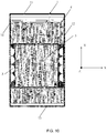
- the above arrangement can be understood in this way: digging the wider metal wall of the battery chamber along the Y-axis direction, such that the battery chamber forms an integrally concave reflection curved surface (which may be a paraboloid) that has opening portions facing a slot array formed by the plurality of slots 15.
- the integrally concave reflection curved surface is formed along the Y axis on the XZ plane, and the plurality of slots 15 are still on the fourth side 14 of the metal frame 1. That is, the slot array formed by the plurality of slots 15 is not at a same X position as the concave reflection curved surface.
- an upper edge of the signal reflection wall is not lower than upper edges of the slots, and a lower edge of the signal reflection wall is not higher than lower edges of the slots.
- the upper edge of the signal reflection wall 3 is not lower than the upper edges of the slots 15, and the lower edge of the signal reflection wall 3 is not higher than the lower edges of the slots 15, so that the signal reflection wall 3 formed by the metal wall of the battery chamber may well cover the slots 15 to facilitate better reflection of signals.
- FIGS. 6 and 7 there are at least four slots 15 on the fourth side 14 of the metal frame 1, and a length of a slot 15 is L1.
- L1 may be approximately half of a wavelength corresponding to a center frequency of an operating frequency band of the millimeter-wave antenna.
- a width H1 of the slot 15 is not limited.
- a distance between edges of the slots 15 is W1, and the distance W1 may be determined by an isolation between two adjacent antennas and a beam scanning coverage angle of the millimeter-wave antenna array.
- a thickness of the battery chamber is H2
- the battery chamber and the slots 15 are on a same side of the ground plate 4, and H2 is greater than or equal to H1.
- H2 is greater than or equal to H1.
- the upper edge of the signal reflection wall 3 formed by the metal wall of the battery chamber may be set no lower than the upper edges of the slots 15, and the lower edge of the signal reflection wall 3 may be set no higher than the lower edges of the slots 15. Therefore, the slots 15 may be covered well to facilitate better reflection of signals.
- the signal reflection wall 3 includes at least two reflection curved surfaces that are in a one-to-one correspondence with arrangement positions of the slots.
- one reflection curved surface may be provided for each slot 15 to facilitate better reflection of signals.
- a length of a slot 15 is L1, and there are at least four slots 15 on the fourth side 14 of the metal frame 1.
- a length of a reflection curved surface is L2, and there are at least four reflection curved surfaces.
- each reflection curved surface may correspond to one slot 15 to facilitate better reflection of signals.
- the number of reflection curved surfaces may be greater than or equal to the number of slots 15, so as to ensure that each slot 15 can correspond to one reflection curved surface. It will be noted that an interface of adjacent reflection curved surfaces may be connected to the fourth side 14, or may not be connected to the fourth side 14.
- L2 may be set to be greater than or equal to L1.
- a convex portion of each reflection curved surface may point to a corresponding slot 15, and there is a certain distance between the convex portion and the slot 15.
- the reflection curved surface is a paraboloid, and a focus of the paraboloid coincides with a midpoint of a slot corresponding to an arrangement position of the paraboloid.
- antenna gain and beam directivity may be improved.
- the at least two slots 15 are arranged along a length direction of the metal frame 1, a length of each slot 15 is the same, and a distance between any two adjacent slots 15 is the same.
- the at least two slots 15 are arranged along the length direction of the metal frame 1, the length of each slot 15 is the same, and the distance between any two adjacent slots 15 is the same, so that the at least two slots 15 can form a slot group to facilitate better radiation of millimeter-wave signals.
- the distance between two adjacent slots 15 is determined by the isolation between two adjacent antennas and the beam scanning coverage angle of the antenna array.
- the distance between two adjacent slots 15 is determined by the isolation between two adjacent antennas and the beam scanning coverage angle of the antenna array, so that the millimeter-wave signals may be better matched for operation.
- the slot 15 includes a first sub-slot 151 and a second sub-slot 152 that are intersected with each other.
- the slot 15 includes the first sub-slot 151 and the second sub-slot 152 that are intersected with each other. In this way, 15 may have horizontal polarization performance and vertical polarization performance.
- the signal reflection wall includes a first reflection curved surface 31 that is concave and corresponds to the first sub-slot 151, and a second reflection curved surface 32 that is concave and corresponds to the second sub-slot 152.
- a generatrix forming the first reflection curved surface 31 is intersected with a generatrix forming the second reflection curved surface 32.
- FIG. 9 is a schematic diagram provided by some embodiments of the present disclosure showing a structure of a reflection curved surface.
- the fourth side 14 is shown by the dotted line in the figure, and three slots 15 are provided on the fourth side.
- Each slot includes a first sub-slot 151 and a second sub-slot 152.
- a reflection curved surface corresponding to the first sub-slot 151 is the first reflection curved surface 31, and the first reflection curved surface 31 is a larger concave curved surface.
- a curved surface corresponding to the second sub-slot 152 is a second reflection curved surface 32, and three second reflection curved surfaces 32 are provided on the first reflection curved surface 31.
- the second reflection curved surfaces 32 are smaller concave curved surfaces, and each second reflection curved surface 32 corresponds to one slot 15.
- the generatrix forming the first reflection curved surface 31 is intersected with the generatrix forming the second reflection curved surface 32.
- the above arrangement may be understood in this way: as shown in FIG. 9 , digging the wider metal wall of the battery chamber along the Y-axis direction, such that the metal wall of the battery chamber forms a concave first reflection curved surface 31 and a plurality of concave second reflection curved surfaces 32.
- the first reflection curved surface 31 is a paraboloid formed along the Y axis on the XZ plane of the coordinate system of the terminal device
- the second reflection curved surface 32 is a paraboloid formed along the Z axis on the XY plane of the coordinate system of the terminal device
- the first reflection curved surface 31 is orthogonal to the plurality of second reflection curved surfaces 32.
- a plurality of slots 15 are provided on the fourth side 14 of the metal frame 1, and each slot 15 has horizontal polarization performance and vertical polarization performance. Opening directions of the first reflection curved surface 31 and the plurality of second reflection curved surfaces 32 both point to the slot group formed by the plurality of slots 15, the plurality of second reflection curved surfaces 32 are in a one-to-one correspondence with the plurality of slots 15, and the slot array formed by the plurality of slots 15 is not at a same X position as the plurality of second reflection curved surfaces 32 (both the first reflection curved surface 31 and the second reflection curved surfaces 32 may be paraboloids).
- the millimeter-wave antenna array formed by the slot group has both horizontal polarization performance and vertical polarization performance, which improves wireless connection capability.
- a parabolic design may further improve coverage of a scanning angle of the main lobe.
- a long side of the first sub-slot 151 is orthogonal to a long side of the second sub-slot 152, and/or the generatrix forming the first reflection curved surface 31 is orthogonal to the generatrix forming the second reflection curved surface 32.
- the long side of the first sub-slot 151 is orthogonal to the long side of the second sub-slot 152, which may be understood as that the first sub-slot 151 is perpendicular to the second sub-slot 152.
- the generatrix forming the first reflection curved surface 31 is orthogonal to the generatrix forming the second reflection curved surface 32, which may be understood as that the generatrix forming the first reflection curved surface 31 is perpendicular to the generatrix forming the second reflection curved surface 32. Therefore, the horizontal polarization performance and the vertical polarization performance of the slot 15 may be further improved.
- two opposite sides of the metal frame 1 are both provided with at least two slots 15.
- Two opposite sides of the metal frame 1 are both provided with at least two slots 15, and the at least two slots 15 on a same side can form a slot group, so that there is a slot group on both the two opposite sides of the metal frame 1, which may further improve a beam coverage of the millimeter-wave antenna array.
- the following description will be made with reference to FIGS. 10 to 12 .
- the two opposite sides of the terminal device are both provided with a signal reflection wall 3 formed by the metal wall of the battery chamber, and the signal reflection walls 3 on the two sides reflect a signal radiated by the second side 12 and a signal radiated by the fourth side 14, respectively.
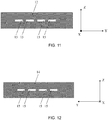
- FIG. 11 It can be seen from FIG. 11 that at least four slots 15 are provided on the second side 12. It can be seen in FIG. 12 that at least four slots 15 are provided on the fourth side 14.
- a main lobe of a millimeter-wave slot array formed by the slots 15 on the second side 12 points to the positive direction of the X axis
- a main lobe of a millimeter-wave slot array formed by the slots 15 on the fourth side 14 points to the negative direction of the X axis, therefore improving the beam coverage of the millimeter-wave antenna array.
- a length of the slot is determined according to a half wavelength corresponding to a center frequency of an antenna operating frequency band.
- the length of the slot 15 may be determined based on a half wavelength corresponding to a center frequency of an antenna operating frequency band.
- the length of the slot 15 may be approximately the half wavelength corresponding to the center frequency of the antenna operating frequency band, so that signals may be better transmitted and received.
- the antenna feedpoint is disposed at a non-central position of an inner side edge of the slot.
- the antenna feedpoint 2 is located at a non-central position of an edge of the slot 15, which may make the millimeter-wave antenna array have better performance.
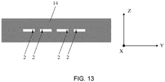
- FIG. 13 there are at least four slots 15 on the fourth side 14, antenna feedpoints 2 of the first slot and the third slot from left to right are proximate to a right side of a center of the slot 15, and antenna feedpoints 2 of the second slot and the at least fourth slot from left to right are proximate to a left side of the center of the slot 15.
- the millimeter-wave antenna array may have better performance.
- this is merely an example of one arrangement of the antenna feedpoints 2, and there may be some other arrangements besides this, and this embodiment is not limited thereto.
- the signal reflection wall 3 may be a reflection plane.
- a width of the gap may be W0, and W0 is greater than 0.
- a length of the gap may be L0, and a total length of the slot group of the antenna array may be Ls, and L0 is greater than or equal to Ls. It will be understood that the gap may be filled with air or a non-conductive material.
- the terminal device provided by some embodiments of the present disclosure includes a metal frame provided with at least two slots on a side. At least two antenna feedpoints are provided on an inner side wall of the metal frame, and different antenna feedpoints in the at least two antenna feedpoints are disposed on side edges of different slots.
- a signal reflection wall is further disposed inside the terminal device, and there is a gap between the signal reflection wall and the at least two slots.
- the signal reflection wall is formed by a metal wall of a battery chamber of the terminal device, wherein the battery chamber is a structure that accommodates a battery of the terminal device.
- the metal frame and the signal reflection wall are both electrically connected to a ground plate of the terminal device.
- the metal frame provided with the slots is equivalent to the millimeter-wave antenna array of the terminal device, and the metal frame is also a radiating body of a communication antenna, and thus the space accommodating the millimeter-wave antenna is saved, which may reduce the volume of the terminal device and support the design of metal appearance better.
- the metal frame may be designed to be compatible with a scheme that the appearance metal serves as other antennas, so as to improve the overall competitiveness of the terminal device.
Landscapes
- Engineering & Computer Science (AREA)
- Computer Networks & Wireless Communication (AREA)
- Physics & Mathematics (AREA)
- Electromagnetism (AREA)
- Computer Hardware Design (AREA)
- General Engineering & Computer Science (AREA)
- Aerials With Secondary Devices (AREA)
- Waveguide Aerials (AREA)
- Variable-Direction Aerials And Aerial Arrays (AREA)
Abstract
Description
- This application claims priority to Chinese Patent Application No.
201810820138.4 - The present disclosure relates to the field of communications technologies, and in particular, to a terminal device.
- With the rapid development of communications technologies, multi-antenna communication has become the mainstream and future development trend of terminal devices, and millimeter-wave antenna arrays are gradually introduced to terminal devices during this process. In the related art, a millimeter-wave antenna array is generally in a form of an independent antenna module, and thus an accommodating space needs to be provided for the independent antenna module in a terminal device, which may cause that the whole terminal device is large in volume and size, thereby resulting in a relatively low overall competitiveness of the terminal device. In addition, for the design of the current mainstream millimeter-wave antenna array, it is usually difficult to show better antenna performance under a design of metal appearance, that is, it is difficult to support the design of metal appearance, and thus the competitiveness of the terminal device is reduced.
- Some embodiments of the present disclosure provide a terminal device to solve a problem of the whole terminal device being large in volume and size, which is caused by that an accommodating space needs to be provided for a millimeter-wave antenna in the terminal device.
- In order to solve the above technical problem, the present disclosure is implemented as follows.
- Some embodiments of the present disclosure provide a terminal device. The terminal device includes a metal frame. At least two slots are disposed on a side of the metal frame. At least two antenna feedpoints are disposed on an inner side wall of the metal frame, and different antenna feedpoints in the at least two antenna feedpoints are disposed on side edges of different slots.
- A signal reflection wall is further disposed inside the terminal device. A gap exists between the signal reflection wall and the at least two slots, and the signal reflection wall is formed by a metal wall of a battery chamber of the terminal device, wherein the battery chamber is a structure accommodating a battery of the terminal device.
- The metal frame and the signal reflection wall are both electrically connected to a ground plate of the terminal device.
- The terminal device provided by some embodiments of the present disclosure includes a metal frame. At least two slots are disposed on a side of the metal frame, at least two antenna feedpoints are provided on an inner side wall of the metal frame, and different antenna feedpoints in the at least two antenna feedpoints are disposed on side edges of different slots. A signal reflection wall is further disposed inside the terminal device, and there is a gap between the signal reflection wall and the at least two slots. The signal reflection wall is formed by a metal wall of a battery chamber of the terminal device, wherein the battery chamber is a structure that accommodates a battery of the terminal device. The metal frame and the signal reflection wall are both electrically connected to a ground plate of the terminal device. In this way, the metal frame provided with the slots is equivalent to a millimeter-wave antenna array of the terminal device, and the metal frame is also a radiating body of a communication antenna, and thus the space accommodating the millimeter-wave antenna is saved, thereby reducing the volume of the terminal device and supporting the design of metal appearance better.
- In order to describe technical solutions in embodiments of the present disclosure more clearly, the accompanying drawings to be used in the description of embodiments of the present disclosure will be introduced briefly below. Obviously, the accompanying drawings in the following description are merely some embodiments of the present disclosure, and a person of ordinary skill in the art may also obtain other drawings according to those drawings without paying any creative effort.
-
FIG. 1 is a first schematic diagram showing a structure of a terminal device, in accordance with some embodiments of the present disclosure; -
FIG. 2 is a first schematic diagram showing a structure of a terminal device, in accordance with some embodiments of the present disclosure; -
FIG. 3 is a first schematic diagram showing a gain azimuth pattern, in accordance with some embodiments of the present disclosure; -
FIG. 4 is a second schematic diagram showing a gain azimuth pattern, in accordance with some embodiments of the present disclosure; -
FIG. 5 is a first schematic diagram showing a structure of a reflection curved surface, in accordance with some embodiments of the present disclosure; -
FIG. 6 is a first schematic diagram showing a structure of a side of a metal frame, in accordance with some embodiments of the present disclosure; -
FIG. 7 is a schematic diagram showing a relative position of a signal reflection wall and a side of a metal frame, in accordance with some embodiments of the present disclosure; -
FIG. 8 is a schematic diagram showing a structure of a slot, in accordance with some embodiments of the present disclosure; -
FIG. 9 is a second schematic diagram showing a structure of a reflection curved surface, in accordance with some embodiments of the present disclosure; -
FIG. 10 is a second schematic diagram showing a structure of a terminal device, in accordance with some embodiments of the present disclosure; -
FIG. 11 is a second schematic diagram showing a structure of a side of a metal frame, in accordance with some embodiments of the present disclosure; -
FIG. 12 is a third schematic diagram showing a structure of a side of a metal frame, in accordance with some embodiments of the present disclosure; and -
FIG. 13 is a schematic diagram of arrangement positions of antenna feedpoints, in accordance with some embodiments of the present disclosure. - Technical solutions in some embodiments of the present disclosure will be described clearly and completely with reference to accompanying drawings in some embodiments of the present disclosure. Obviously, the described embodiments are merely some but not all the embodiments of the present disclosure. All other embodiments obtained on a basis of the embodiments of the present disclosure by a person of ordinary skill in the art without paying any creative effort shall be included in the protection scope of the present disclosure.
- Some embodiments of the present disclosure provide a terminal device. For ease of understanding, the terminal device will be described below with reference to
FIGS. 1 to 13 . - Referring to
FIG. 1 , the terminal device provided by some embodiments of the present disclosure includes ametal frame 1, and at least twoslots 15 are disposed on a side of themetal frame 1. At least twoantenna feedpoints 2 are disposed on an inner side wall of themetal frame 1, and different antenna feedpoints in the at least twoantenna feedpoints 2 are located on side edges ofdifferent slots 15. The terminal device further has asignal reflection wall 3 disposed inside the terminal device, and there is a gap between thesignal reflection wall 3 and the at least twoslots 15. Thesignal reflection wall 3 is formed by a metal wall of abattery chamber 5 of the terminal device. Themetal frame 1 and thesignal reflection wall 3 are both electrically connected to aground plate 4 of the terminal device, and the battery chamber is a structure that accommodates a battery of the terminal device. - In this embodiment, the
metal frame 1 may be a frame with a head portion and a tail portion connected or unconnected, and themetal frame 1 may include afirst side 11, asecond side 12, athird side 13 and afourth side 14. The at least twoslots 15 may be disposed on one side of themetal frame 1. Alternatively, two opposite sides of themetal frame 1 may be both provided with at least twoslots 15. Theslots 15 may be filled with air or a non-conductive material, or the like. - In this embodiment, at least two
antenna feedpoints 2 are disposed on the inner side wall of themetal frame 1, anddifferent antenna feedpoints 2 in the at least twoantenna feedpoints 2 are located on side edges ofdifferent slots 15, so that it may be ensured that there are at least twoslots 15 on a side of themetal frame 1 and each of which has anantenna feedpoint 2, and thus the at least twoslots 15 may form a millimeter-wave antenna array. Theantenna feedpoints 2 of the millimeter-wave antenna array are located on side edges of theslots 15. For example, theantenna feedpoints 2 may be located on a side of centers of theslots 15, so that millimeter-wave signals may be led to theantenna feedpoints 2 of the millimeter-wave antenna array, and are radiated through themetal frame 1. Besides, themetal frame 1 can also receive millimeter-wave signals. Of course, it is optional that eachslot 15 may be provided with anantenna feedpoint 2. - In this embodiment, due to the existence of the
signal reflection wall 3, the performance of the antenna may be enhanced, and the gain of the antenna may be improved. There is a gap between thesignal reflection wall 3 and the at least twoslots 15, and the gap may be filled with air, or some non-conductive materials, or the like. - In this implementation, a side frame of the metal wall of the battery chamber in a length direction of the terminal device may be wider. The
signal reflection wall 3 may be a reflection curved surface that is convex or concave, as shown inFIG. 1 . Thesignal reflection wall 3 may also be a flat surface, as shown inFIG. 2 . Generally, the terminal device has a battery chamber, and thus the metal wall of the battery chamber is directly used as a signal reflection wall, which makes it unnecessary to add additional materials, thereby saving the cost of the terminal device. - In this embodiment, the
battery chamber 5 may be disposed above theground plate 4, and the metal wall of thebattery chamber 5 serves as thesignal reflection wall 3 of the antenna (e.g., the millimeter-wave antenna array). Theground plate 4 may be a circuit board, a metal housing or a screen, etc. Themetal frame 1 and thesignal reflection wall 3 are both electrically connected to theground plate 4 of the terminal device, so that themetal frame 1 and thesignal reflection wall 3 may be grounded. - In this embodiment, the performance of the millimeter-wave antenna array may be enhanced by directly using the metal wall of the battery chamber as the
signal reflection wall 3. Referring toFIGS. 3 and4 , the gain azimuth pattern shown byFIG. 3 is a gain azimuth pattern of an antenna array when there is no battery chamber or the battery chamber has no special design. The gain azimuth pattern shown byFIG. 4 is the gain azimuth pattern of an antenna array when the battery chamber has a special design (e.g., a parabolic design) and is disposed near a millimeter-wave slot antenna array. Scales inFIGS. 3 and4 show an increase in gain from the zero scales upwards and a decrease from the zero scales downwards. - In
FIG. 3 , a gain in a positive direction and a negative direction of the X axis are larger, and a gain near the origin of coordinates is smaller. ForFIG. 3 , a gain of a back lobe (the positive direction of the X axis) is larger than a gain of a positive direction of the X axis inFIG. 4 , and thus a beamwidth of a main lobe (the negative direction of the X axis) inFIG. 3 is narrower than a beamwidth of a main lobe (a negative direction of the X axis) inFIG. 4 , and a gain of the main lobe inFIG. 3 is smaller than the gain of the main lobe inFIG. 4 . - In
FIG. 4 , a gain in a negative direction of the X axis is larger, and a gain near the origin of coordinates is smaller. ForFIG. 4 , a gain of a back lobe (the positive direction of the X axis) is smaller than the gain of the positive direction of the X axis inFIG. 3 , and thus the beamwidth of the main lobe (the negative direction of the X axis) inFIG. 4 is wider than the beamwidth of the main lobe (the negative direction of the X axis) inFIG. 3 , and the gain of the main lobe inFIG. 4 is larger than the gain of the main lobe inFIG. 3 . - In this way, in some embodiments of the present disclosure, at least two
slots 15 are provided on a side of the metal frame of the terminal device, which is equivalent to forming a millimeter-wave antenna array, and which may save the space accommodating the millimeter-wave antenna array without occupying antenna space of other antennas, and may further reduce a volume of the terminal device, and thus overall competitiveness of the terminal device may be improved. In addition, taking advantage of the structure of the terminal device as the antenna improves the communication effect, and does not affect the metal texture of the terminal device. Moreover, using the metal wall of the battery chamber directly as thesignal reflection wall 3 may enhance the performance of the millimeter-wave antenna array, improve the gain of the millimeter-wave antenna array, and optimize the gain azimuth pattern of the antenna array. What is more, it is also unnecessary to add additional materials, which may save the cost of the terminal. - In addition, for the design of the current mainstream millimeter-wave antenna array, it is usually difficult to show better antenna performance under a design of metal appearance, that is, it is difficult to support the design of metal appearance, and thus the competitiveness of the terminal device is reduced. The design of the embodiment may better support the design of metal appearance, and may be compatible with a scheme that the appearance metal serves as other antennas, so as to improve the overall competitiveness of the product. The terminal device provided by some embodiments of the present disclosure not only solves a problem of the whole terminal device being large in volume and size, which is caused by that an accommodating space needs to be provided for a millimeter-wave antenna in the terminal device, but also solves a problem that it is difficult for the terminal device to support the design of metal appearance.
- In some embodiments of the present disclosure, the terminal device may be a mobile phone, a tablet personal computer, a laptop computer, a personal digital assistant (PDA), a mobile Internet device (MID), a wearable device, or the like.
- Optionally, the
signal reflection wall 3 is a concave reflection curved surface. - In this embodiment, a directivity of an antenna signal may be improved by reflecting the antenna signal through the reflection curved surface.
- Optionally, the reflection curved surface is formed by a generatrix parallel to a length direction of the metal frame; or the reflection curved surface is formed by a generatrix parallel to a width direction of the metal frame.
- In this implementation, the reflection curved surface is formed by the generatrix parallel to the length direction of the metal frame. For example, referring to
FIG. 5 , the reflection curved surface is a paraboloid formed along the Y axis on the XZ plane of the coordinate system of the terminal device. Alternatively, the reflection curved surface is formed by the generatrix parallel to the width direction of the metal frame. For example, referring toFIG. 1 , the reflection curved surface is a paraboloid formed along the Z axis on the XY plane of the coordinate system of the terminal device. In this way, a plurality of arrangements of the reflection curved surface are provided for the terminal device, and the terminal device can select an appropriate arrangement according to actual needs. - Optionally, the reflection curved surface is a paraboloid.
- In order to better understand that the reflection curved surface is a paraboloid, reference can be made to
FIG. 5 . Thefourth side 14 is shown by the dotted line in the figure, and at least fourslots 15 are provided on thefourth side 14. A concave paraboloid is located at a position near thefourth side 14. The paraboloid is thesignal reflection wall 3 formed by the metal wall of the battery chamber of the terminal device, and can be used to reflect millimeter-wave signals radiated by thefourth side 14. By designing the reflection curved surface as a paraboloid, the gain of the antenna may be optimized. - And the above arrangement can be understood in this way: digging the wider metal wall of the battery chamber along the Y-axis direction, such that the battery chamber forms an integrally concave reflection curved surface (which may be a paraboloid) that has opening portions facing a slot array formed by the plurality of
slots 15. The integrally concave reflection curved surface is formed along the Y axis on the XZ plane, and the plurality ofslots 15 are still on thefourth side 14 of themetal frame 1. That is, the slot array formed by the plurality ofslots 15 is not at a same X position as the concave reflection curved surface. - Optionally, an upper edge of the signal reflection wall is not lower than upper edges of the slots, and a lower edge of the signal reflection wall is not higher than lower edges of the slots.
- In this implementation, the upper edge of the
signal reflection wall 3 is not lower than the upper edges of theslots 15, and the lower edge of thesignal reflection wall 3 is not higher than the lower edges of theslots 15, so that thesignal reflection wall 3 formed by the metal wall of the battery chamber may well cover theslots 15 to facilitate better reflection of signals. - In order to better understand the above arrangement, reference may be made to
FIGS. 6 and7 . As can be seen fromFIG. 6 , there are at least fourslots 15 on thefourth side 14 of themetal frame 1, and a length of aslot 15 is L1. L1 may be approximately half of a wavelength corresponding to a center frequency of an operating frequency band of the millimeter-wave antenna. A width H1 of theslot 15 is not limited. A distance between edges of theslots 15 is W1, and the distance W1 may be determined by an isolation between two adjacent antennas and a beam scanning coverage angle of the millimeter-wave antenna array. InFIG. 7 , a thickness of the battery chamber is H2, the battery chamber and theslots 15 are on a same side of theground plate 4, and H2 is greater than or equal to H1. In this way, the upper edge of thesignal reflection wall 3 formed by the metal wall of the battery chamber may be set no lower than the upper edges of theslots 15, and the lower edge of thesignal reflection wall 3 may be set no higher than the lower edges of theslots 15. Therefore, theslots 15 may be covered well to facilitate better reflection of signals. - Optionally, the
signal reflection wall 3 includes at least two reflection curved surfaces that are in a one-to-one correspondence with arrangement positions of the slots. - In this implementation, one reflection curved surface may be provided for each
slot 15 to facilitate better reflection of signals. In order to better understand the above arrangement, reference may also be made toFIGS. 6 and7 . InFIG. 7 , a length of aslot 15 is L1, and there are at least fourslots 15 on thefourth side 14 of themetal frame 1. InFIG. 7 , a length of a reflection curved surface is L2, and there are at least four reflection curved surfaces. In this way, each reflection curved surface may correspond to oneslot 15 to facilitate better reflection of signals. Of course, the number of reflection curved surfaces may be greater than or equal to the number ofslots 15, so as to ensure that eachslot 15 can correspond to one reflection curved surface. It will be noted that an interface of adjacent reflection curved surfaces may be connected to thefourth side 14, or may not be connected to thefourth side 14. - In order to make a reflection curved surface corresponding to each
slot 15 better cover theslot 15, L2 may be set to be greater than or equal to L1. In addition, a convex portion of each reflection curved surface may point to acorresponding slot 15, and there is a certain distance between the convex portion and theslot 15. - Optionally, the reflection curved surface is a paraboloid, and a focus of the paraboloid coincides with a midpoint of a slot corresponding to an arrangement position of the paraboloid.
- In this embodiment, by coinciding the focus of the paraboloid with the midpoint of the slot corresponding to the arrangement position of the paraboloid, antenna gain and beam directivity may be improved.
- Optionally, the at least two
slots 15 are arranged along a length direction of themetal frame 1, a length of eachslot 15 is the same, and a distance between any twoadjacent slots 15 is the same. - In this implementation, the at least two
slots 15 are arranged along the length direction of themetal frame 1, the length of eachslot 15 is the same, and the distance between any twoadjacent slots 15 is the same, so that the at least twoslots 15 can form a slot group to facilitate better radiation of millimeter-wave signals. - Optionally, the distance between two
adjacent slots 15 is determined by the isolation between two adjacent antennas and the beam scanning coverage angle of the antenna array. - In this implementation, the distance between two
adjacent slots 15 is determined by the isolation between two adjacent antennas and the beam scanning coverage angle of the antenna array, so that the millimeter-wave signals may be better matched for operation. - Optionally, the
slot 15 includes afirst sub-slot 151 and asecond sub-slot 152 that are intersected with each other. - In order to better understand the above arrangement, reference may be made to
FIG. 8 , and theslot 15 includes thefirst sub-slot 151 and thesecond sub-slot 152 that are intersected with each other. In this way, 15 may have horizontal polarization performance and vertical polarization performance. - Optionally, the signal reflection wall includes a first reflection curved
surface 31 that is concave and corresponds to thefirst sub-slot 151, and a second reflection curvedsurface 32 that is concave and corresponds to thesecond sub-slot 152. A generatrix forming the first reflection curvedsurface 31 is intersected with a generatrix forming the second reflection curvedsurface 32. - In this implementation, in order to better understand the above arrangement, reference can be made to
FIG. 9, and FIG. 9 is a schematic diagram provided by some embodiments of the present disclosure showing a structure of a reflection curved surface. InFIG. 9 , thefourth side 14 is shown by the dotted line in the figure, and threeslots 15 are provided on the fourth side. Each slot includes afirst sub-slot 151 and asecond sub-slot 152. A reflection curved surface corresponding to thefirst sub-slot 151 is the first reflection curvedsurface 31, and the first reflection curvedsurface 31 is a larger concave curved surface. A curved surface corresponding to thesecond sub-slot 152 is a second reflection curvedsurface 32, and three second reflection curved surfaces 32 are provided on the first reflection curvedsurface 31. The second reflection curved surfaces 32 are smaller concave curved surfaces, and each second reflection curvedsurface 32 corresponds to oneslot 15. The generatrix forming the first reflection curvedsurface 31 is intersected with the generatrix forming the second reflection curvedsurface 32. - Or the above arrangement may be understood in this way: as shown in
FIG. 9 , digging the wider metal wall of the battery chamber along the Y-axis direction, such that the metal wall of the battery chamber forms a concave first reflection curvedsurface 31 and a plurality of concave second reflection curved surfaces 32. The first reflection curvedsurface 31 is a paraboloid formed along the Y axis on the XZ plane of the coordinate system of the terminal device, the second reflection curvedsurface 32 is a paraboloid formed along the Z axis on the XY plane of the coordinate system of the terminal device, and the first reflection curvedsurface 31 is orthogonal to the plurality of second reflection curved surfaces 32. A plurality ofslots 15 are provided on thefourth side 14 of themetal frame 1, and eachslot 15 has horizontal polarization performance and vertical polarization performance. Opening directions of the first reflection curvedsurface 31 and the plurality of second reflection curved surfaces 32 both point to the slot group formed by the plurality ofslots 15, the plurality of second reflection curved surfaces 32 are in a one-to-one correspondence with the plurality ofslots 15, and the slot array formed by the plurality ofslots 15 is not at a same X position as the plurality of second reflection curved surfaces 32 (both the first reflection curvedsurface 31 and the second reflection curved surfaces 32 may be paraboloids). - In this implementation, the millimeter-wave antenna array formed by the slot group has both horizontal polarization performance and vertical polarization performance, which improves wireless connection capability. Moreover, a parabolic design may further improve coverage of a scanning angle of the main lobe.
- Optionally, a long side of the
first sub-slot 151 is orthogonal to a long side of thesecond sub-slot 152, and/or the generatrix forming the first reflection curvedsurface 31 is orthogonal to the generatrix forming the second reflection curvedsurface 32. - In this implementation, the long side of the
first sub-slot 151 is orthogonal to the long side of thesecond sub-slot 152, which may be understood as that thefirst sub-slot 151 is perpendicular to thesecond sub-slot 152. The generatrix forming the first reflection curvedsurface 31 is orthogonal to the generatrix forming the second reflection curvedsurface 32, which may be understood as that the generatrix forming the first reflection curvedsurface 31 is perpendicular to the generatrix forming the second reflection curvedsurface 32. Therefore, the horizontal polarization performance and the vertical polarization performance of theslot 15 may be further improved. - Optionally, two opposite sides of the
metal frame 1 are both provided with at least twoslots 15. - Two opposite sides of the
metal frame 1 are both provided with at least twoslots 15, and the at least twoslots 15 on a same side can form a slot group, so that there is a slot group on both the two opposite sides of themetal frame 1, which may further improve a beam coverage of the millimeter-wave antenna array. In order to better understand the above arrangement, the following description will be made with reference toFIGS. 10 to 12 . - As shown in
FIG. 10 , the two opposite sides of the terminal device are both provided with asignal reflection wall 3 formed by the metal wall of the battery chamber, and thesignal reflection walls 3 on the two sides reflect a signal radiated by thesecond side 12 and a signal radiated by thefourth side 14, respectively. It can be seen fromFIG. 11 that at least fourslots 15 are provided on thesecond side 12. It can be seen inFIG. 12 that at least fourslots 15 are provided on thefourth side 14. In this way, a main lobe of a millimeter-wave slot array formed by theslots 15 on thesecond side 12 points to the positive direction of the X axis, and a main lobe of a millimeter-wave slot array formed by theslots 15 on thefourth side 14 points to the negative direction of the X axis, therefore improving the beam coverage of the millimeter-wave antenna array. - Optionally, a length of the slot is determined according to a half wavelength corresponding to a center frequency of an antenna operating frequency band.
- In this implementation, the length of the
slot 15 may be determined based on a half wavelength corresponding to a center frequency of an antenna operating frequency band. For example, the length of theslot 15 may be approximately the half wavelength corresponding to the center frequency of the antenna operating frequency band, so that signals may be better transmitted and received. - Optionally, the antenna feedpoint is disposed at a non-central position of an inner side edge of the slot.
- In this implementation, the
antenna feedpoint 2 is located at a non-central position of an edge of theslot 15, which may make the millimeter-wave antenna array have better performance. In order to better understand the above arrangement, the following description will be made with reference toFIG. 13 . As shown inFIG. 13 , there are at least fourslots 15 on thefourth side 14, antenna feedpoints 2 of the first slot and the third slot from left to right are proximate to a right side of a center of theslot 15, andantenna feedpoints 2 of the second slot and the at least fourth slot from left to right are proximate to a left side of the center of theslot 15. The millimeter-wave antenna array may have better performance. Of course, this is merely an example of one arrangement of theantenna feedpoints 2, and there may be some other arrangements besides this, and this embodiment is not limited thereto. - Optionally, the
signal reflection wall 3 may be a reflection plane. - For example, as shown in
FIG. 2 , there is a gap between the metal wall of the battery chamber and themetal frame 1. A width of the gap may be W0, and W0 is greater than 0. A length of the gap may be L0, and a total length of the slot group of the antenna array may be Ls, and L0 is greater than or equal to Ls. It will be understood that the gap may be filled with air or a non-conductive material. By using the metal wall of the battery chamber as thesignal reflection wall 3, not only may an azimuth pattern of the antenna array be optimized, but also the implementation is simpler. - The terminal device provided by some embodiments of the present disclosure includes a metal frame provided with at least two slots on a side. At least two antenna feedpoints are provided on an inner side wall of the metal frame, and different antenna feedpoints in the at least two antenna feedpoints are disposed on side edges of different slots. A signal reflection wall is further disposed inside the terminal device, and there is a gap between the signal reflection wall and the at least two slots. The signal reflection wall is formed by a metal wall of a battery chamber of the terminal device, wherein the battery chamber is a structure that accommodates a battery of the terminal device. The metal frame and the signal reflection wall are both electrically connected to a ground plate of the terminal device. In this way, the metal frame provided with the slots is equivalent to the millimeter-wave antenna array of the terminal device, and the metal frame is also a radiating body of a communication antenna, and thus the space accommodating the millimeter-wave antenna is saved, which may reduce the volume of the terminal device and support the design of metal appearance better. Furthermore, the metal frame may be designed to be compatible with a scheme that the appearance metal serves as other antennas, so as to improve the overall competitiveness of the terminal device.
- It will be noted that, the terms such as "include" and "comprise" or any other variation thereof herein are intended to cover non-exclusive inclusion, so that a process, a method, an article or an apparatus that includes a series of elements that not only includes those elements, but also includes other elements not explicitly listed or elements inherent to the process, the method, the article or the apparatus. In a case where there is no more limitation, an element defined by the phrase "including a..." does not exclude existence of other identical elements in a process, a method, an article or an apparatus that includes the element.
- The embodiments of the present disclosure are described above with reference to the accompanying drawings. However, the present disclosure is not limited to the above specific embodiments. The above specific embodiments are merely examples and are not restrictive. Under enlightenment of the present disclosure, a person of ordinary skill in the art may make a plurality of forms without departing from spirit of the present disclosure and the protection scope of the claims, all of which shall be included in the protection scope of the present disclosure.
Claims (17)
- A terminal device, comprising a metal frame with at least two slots disposed on a side of the metal frame, at least two antenna feedpoints being disposed on an inner side wall of the metal frame, and different antenna feedpoints in the at least two antenna feedpoints being disposed on side edges of different slots;
a signal reflection wall being further disposed inside the terminal device, a gap existing between the signal reflection wall and the at least two slots, and the signal reflection wall being formed by a metal wall of a battery chamber of the terminal device; wherein the battery chamber is a structure accommodating a battery of the terminal device; and
the metal frame and the signal reflection wall are both electrically connected to a ground plate of the terminal device. - The terminal device according to claim 1, wherein the signal reflection wall is a concave reflection curved surface.
- The terminal device according to claim 2, wherein the reflection curved surface is formed by a generatrix parallel to a length direction of the metal frame; or the reflection curved surface is formed by a generatrix parallel to a width direction of the metal frame.
- The terminal device according to claim 2, wherein the reflection curved surface is a paraboloid.
- The terminal device according to claim 1, wherein an upper edge of the signal reflection wall is not lower than upper edges of the slots, and a lower edge of the signal reflection wall is not higher than lower edges of the slots.
- The terminal device according to any one of claims 1 to 5, wherein the signal reflection wall comprises at least two reflection curved surfaces that are in one-to-one correspondence with arrangement positions of the slots.
- The terminal device according to claim 6, wherein the reflection curved surfaces are paraboloids, and focuses of the paraboloids coincide with midpoints of slots corresponding to arrangement positions of the paraboloids.
- The terminal device according to claim 6, wherein the at least two slots are arranged in a length direction of the metal frame, each slot has a same length, and there is a same distance between any two adjacent slots.
- The terminal device according to claim 8, wherein the distance between two adjacent slots is determined by an isolation between two adjacent antennas and a beam scanning coverage angle of an antenna array.
- The terminal device according to any one of claims 1 to 5, wherein a slot comprises a first sub-slot and a second sub-slot that are intersected with each other.
- The terminal device according to claim 10, wherein the signal reflection wall comprises a first reflection curved surface that is concave and corresponds to the first sub-slot, and a second reflection curved surface that is concave and corresponds to the second sub-slot; and a generatrix forming the first reflection curved surface is intersected with a generatrix forming the second reflection curved surface.
- The terminal device according to claim 11, wherein a long side of the first sub-slot is orthogonal to a long side of the second sub-slot; and/or a generatrix forming the first reflection curved surface is orthogonal to a generatrix forming the second reflection curved surface.
- The terminal device according to claim 1, wherein two opposite sides of the metal frame are both provided with at least two slots.
- The terminal device according to claim 1, wherein a length of a slot is determined according to a half wavelength corresponding to a center frequency of an operating frequency band of an antenna.
- The terminal device according to claim 1, wherein an antenna feedpoint is disposed at a non-central position of an inner side edge of a slot.
- The terminal device according to claim 1, wherein
the metal frame is a radiating body of a communication antenna. - A terminal device, comprising a radiating body of a communication antenna, a millimeter-wave antenna array being disposed on the radiating body.
Applications Claiming Priority (2)
| Application Number | Priority Date | Filing Date | Title |
|---|---|---|---|
| CN201810820138.4A CN108987944B (en) | 2018-07-24 | 2018-07-24 | a terminal device |
| PCT/CN2019/096685 WO2020020055A1 (en) | 2018-07-24 | 2019-07-19 | Terminal device |
Publications (3)
| Publication Number | Publication Date |
|---|---|
| EP3828998A1 true EP3828998A1 (en) | 2021-06-02 |
| EP3828998A4 EP3828998A4 (en) | 2021-08-04 |
| EP3828998B1 EP3828998B1 (en) | 2022-11-23 |
Family
ID=64550034
Family Applications (1)
| Application Number | Title | Priority Date | Filing Date |
|---|---|---|---|
| EP19840579.7A Active EP3828998B1 (en) | 2018-07-24 | 2019-07-19 | Terminal device |
Country Status (5)
| Country | Link |
|---|---|
| US (1) | US11527812B2 (en) |
| EP (1) | EP3828998B1 (en) |
| CN (1) | CN108987944B (en) |
| ES (1) | ES2932957T3 (en) |
| WO (1) | WO2020020055A1 (en) |
Families Citing this family (7)
| Publication number | Priority date | Publication date | Assignee | Title |
|---|---|---|---|---|
| CN108987945B (en) | 2018-07-24 | 2020-08-04 | 维沃移动通信有限公司 | a terminal device |
| CN108987905B (en) * | 2018-07-24 | 2021-01-08 | 维沃移动通信有限公司 | Terminal equipment |
| CN108987944B (en) | 2018-07-24 | 2021-04-23 | 维沃移动通信有限公司 | a terminal device |
| CN110098466B (en) * | 2019-04-26 | 2021-11-16 | 维沃移动通信有限公司 | Terminal equipment |
| CN112310653B (en) * | 2019-07-31 | 2023-04-25 | Oppo广东移动通信有限公司 | Electronic equipment |
| CN113497343A (en) * | 2020-03-20 | 2021-10-12 | 北京小米移动软件有限公司 | Antenna structure and electronic device |
| US12493570B2 (en) * | 2023-09-26 | 2025-12-09 | Microchip Technology Incorporated | Device and methods for functional descriptor-based DMA controller |
Family Cites Families (32)
| Publication number | Priority date | Publication date | Assignee | Title |
|---|---|---|---|---|
| JP3626618B2 (en) * | 1999-03-04 | 2005-03-09 | アルプス電気株式会社 | Converter for satellite broadcasting reception |
| JP3916068B2 (en) * | 2002-11-06 | 2007-05-16 | ソニー・エリクソン・モバイルコミュニケーションズ株式会社 | Wireless device |
| EP2025045B1 (en) | 2006-05-23 | 2011-05-11 | Intel Corporation | Chip-lens array antenna system |
| US8896487B2 (en) * | 2009-07-09 | 2014-11-25 | Apple Inc. | Cavity antennas for electronic devices |
| CN201590480U (en) * | 2009-12-30 | 2010-09-22 | 中兴通讯股份有限公司 | Handheld terminal and power supply battery |
| TWI429138B (en) * | 2010-03-25 | 2014-03-01 | Htc Corp | Planar bidirectional radiation antenna |
| US8754822B1 (en) * | 2010-08-17 | 2014-06-17 | Amazon Technologies, Inc. | Tuning elements for specific absorption rate reduction |
| JP2013115648A (en) * | 2011-11-29 | 2013-06-10 | Dexerials Corp | Antenna device and communication device |
| CN102544693A (en) * | 2012-01-20 | 2012-07-04 | 苏州佳世达电通有限公司 | Action electronic device |
| US8836587B2 (en) * | 2012-03-30 | 2014-09-16 | Apple Inc. | Antenna having flexible feed structure with components |
| KR102013588B1 (en) * | 2012-09-19 | 2019-08-23 | 엘지전자 주식회사 | Mobile terminal |
| KR102033311B1 (en) * | 2013-11-22 | 2019-10-17 | 현대모비스 주식회사 | Microstripline-fed slot array antenna and manufacturing method thereof |
| CN104282982A (en) * | 2014-10-20 | 2015-01-14 | 国网河南省电力公司漯河供电公司 | Computer battery plate with built-tin antenna |
| CN104901004B (en) * | 2015-06-01 | 2017-07-28 | 电子科技大学 | A kind of high-gain end-fire millimeter wave antenna |
| CN105337022B (en) * | 2015-10-19 | 2018-01-19 | 广东欧珀移动通信有限公司 | An LTE‑A MIMO antenna device with an all-metal casing |
| CN106935962B (en) | 2015-12-30 | 2020-02-14 | 华为技术有限公司 | Terminal device and antenna |
| WO2017122905A1 (en) * | 2016-01-11 | 2017-07-20 | Samsung Electronics Co., Ltd. | Wireless communication device with leaky-wave phased array antenna |
| KR102466002B1 (en) * | 2016-04-19 | 2022-11-11 | 삼성전자주식회사 | Electronic device including antenna |
| CN105789904B (en) | 2016-05-03 | 2019-01-25 | 南京信息职业技术学院 | A slot antenna based on rectangular slot waveguide |
| KR102465796B1 (en) * | 2016-05-27 | 2022-11-10 | 삼성전자주식회사 | Electronic device with multi-slot antenna |
| CN105933481A (en) * | 2016-06-29 | 2016-09-07 | 努比亚技术有限公司 | Antenna structure and mobile terminal |
| CN106785384A (en) * | 2016-11-30 | 2017-05-31 | 中国铁塔股份有限公司长春市分公司 | A kind of anti-interference antenna |
| CN106454608A (en) * | 2016-12-05 | 2017-02-22 | 深圳市科奈信科技有限公司 | Low-loss wireless Bluetooth headset |
| CN108270080A (en) * | 2017-01-03 | 2018-07-10 | 深圳市信维通信股份有限公司 | Millimeter wave array antenna system based on metal fuselage |
| CN206412466U (en) * | 2017-01-03 | 2017-08-15 | 深圳市信维通信股份有限公司 | Millimeter wave antenna and its antenna system |
| CN206370500U (en) * | 2017-01-19 | 2017-08-01 | 深圳市玛雅通讯设备有限公司 | Antenna structure based on battery of mobile phone bonnet |
| CN107317097B (en) * | 2017-07-03 | 2020-01-17 | 昆山睿翔讯通通信技术有限公司 | Millimeter wave array and non-millimeter wave integrated antenna |
| CN207624903U (en) | 2017-10-27 | 2018-07-17 | 上海安费诺永亿通讯电子有限公司 | A kind of compact double antenna unit and its mimo antenna system for becket mobile phone |
| CN108987906B (en) * | 2018-07-24 | 2021-01-08 | 维沃移动通信有限公司 | Terminal equipment |
| CN108987944B (en) * | 2018-07-24 | 2021-04-23 | 维沃移动通信有限公司 | a terminal device |
| CN108987905B (en) * | 2018-07-24 | 2021-01-08 | 维沃移动通信有限公司 | Terminal equipment |
| CN108987945B (en) * | 2018-07-24 | 2020-08-04 | 维沃移动通信有限公司 | a terminal device |
-
2018
- 2018-07-24 CN CN201810820138.4A patent/CN108987944B/en active Active
-
2019
- 2019-07-19 ES ES19840579T patent/ES2932957T3/en active Active
- 2019-07-19 EP EP19840579.7A patent/EP3828998B1/en active Active
- 2019-07-19 WO PCT/CN2019/096685 patent/WO2020020055A1/en not_active Ceased
-
2021
- 2021-01-22 US US17/156,143 patent/US11527812B2/en active Active
Also Published As
| Publication number | Publication date |
|---|---|
| ES2932957T3 (en) | 2023-01-30 |
| CN108987944A (en) | 2018-12-11 |
| EP3828998B1 (en) | 2022-11-23 |
| US20210143528A1 (en) | 2021-05-13 |
| US11527812B2 (en) | 2022-12-13 |
| WO2020020055A1 (en) | 2020-01-30 |
| EP3828998A4 (en) | 2021-08-04 |
| CN108987944B (en) | 2021-04-23 |
Similar Documents
| Publication | Publication Date | Title |
|---|---|---|
| US11527812B2 (en) | Terminal device | |
| US11355831B2 (en) | Antenna system and mobile terminal | |
| EP3828995B1 (en) | Terminal device | |
| AU2021215154A1 (en) | Communication device | |
| EP3905441A1 (en) | Antenna structure and high-frequency multi-band wireless communication terminal | |
| US11962066B2 (en) | Terminal device | |
| WO2020020056A1 (en) | Terminal device | |
| EP3806240B1 (en) | Antenna | |
| CN111864362A (en) | Antenna modules and electronic equipment | |
| EP3905435A1 (en) | Antenna structure and terminal | |
| US12107321B2 (en) | Antenna and electronic device including same | |
| CN111864343A (en) | Electronic equipment | |
| WO2022228188A1 (en) | Antenna array, antenna module, and electronic device | |
| WO2021233353A1 (en) | Antenna apparatus and radio communication device | |
| CN114665265A (en) | Electronic device | |
| CN119325669B (en) | Antenna structure | |
| CN113839170B (en) | Antenna Module and Mobile Terminal | |
| CN113571882A (en) | Communication equipment | |
| CN120511458A (en) | Electronic equipment | |
| CN122027727A (en) | Electronic equipment | |
| HK40051832B (en) | Communication device | |
| HK40051832A (en) | Communication device | |
| HK40010545A (en) | Communication device |
Legal Events
| Date | Code | Title | Description |
|---|---|---|---|
| STAA | Information on the status of an ep patent application or granted ep patent |
Free format text: STATUS: THE INTERNATIONAL PUBLICATION HAS BEEN MADE |
|
| PUAI | Public reference made under article 153(3) epc to a published international application that has entered the european phase |
Free format text: ORIGINAL CODE: 0009012 |
|
| STAA | Information on the status of an ep patent application or granted ep patent |
Free format text: STATUS: REQUEST FOR EXAMINATION WAS MADE |
|
| 17P | Request for examination filed |
Effective date: 20210223 |
|
| AK | Designated contracting states |
Kind code of ref document: A1 Designated state(s): AL AT BE BG CH CY CZ DE DK EE ES FI FR GB GR HR HU IE IS IT LI LT LU LV MC MK MT NL NO PL PT RO RS SE SI SK SM TR |
|
| A4 | Supplementary search report drawn up and despatched |
Effective date: 20210707 |
|
| RIC1 | Information provided on ipc code assigned before grant |
Ipc: H01Q 1/24 20060101AFI20210701BHEP Ipc: H01Q 21/08 20060101ALI20210701BHEP Ipc: H01Q 19/17 20060101ALI20210701BHEP Ipc: H01Q 1/44 20060101ALI20210701BHEP Ipc: H01Q 13/10 20060101ALI20210701BHEP |
|
| DAV | Request for validation of the european patent (deleted) | ||
| DAX | Request for extension of the european patent (deleted) | ||
| REG | Reference to a national code |
Ref country code: DE Ref legal event code: R079 Ref document number: 602019022358 Country of ref document: DE Free format text: PREVIOUS MAIN CLASS: H01Q0021060000 Ipc: H01Q0001240000 |
|
| GRAP | Despatch of communication of intention to grant a patent |
Free format text: ORIGINAL CODE: EPIDOSNIGR1 |
|
| RIC1 | Information provided on ipc code assigned before grant |
Ipc: H01Q 13/10 20060101ALI20220705BHEP Ipc: H01Q 1/44 20060101ALI20220705BHEP Ipc: H01Q 19/17 20060101ALI20220705BHEP Ipc: H01Q 21/08 20060101ALI20220705BHEP Ipc: H01Q 1/24 20060101AFI20220705BHEP |
|
| STAA | Information on the status of an ep patent application or granted ep patent |
Free format text: STATUS: GRANT OF PATENT IS INTENDED |
|
| INTG | Intention to grant announced |
Effective date: 20220811 |
|
| GRAS | Grant fee paid |
Free format text: ORIGINAL CODE: EPIDOSNIGR3 |
|
| GRAA | (expected) grant |
Free format text: ORIGINAL CODE: 0009210 |
|
| STAA | Information on the status of an ep patent application or granted ep patent |
Free format text: STATUS: THE PATENT HAS BEEN GRANTED |
|
| AK | Designated contracting states |
Kind code of ref document: B1 Designated state(s): AL AT BE BG CH CY CZ DE DK EE ES FI FR GB GR HR HU IE IS IT LI LT LU LV MC MK MT NL NO PL PT RO RS SE SI SK SM TR |
|
| REG | Reference to a national code |
Ref country code: GB Ref legal event code: FG4D |
|
| REG | Reference to a national code |
Ref country code: CH Ref legal event code: EP |
|
| REG | Reference to a national code |
Ref country code: AT Ref legal event code: REF Ref document number: 1533714 Country of ref document: AT Kind code of ref document: T Effective date: 20221215 Ref country code: DE Ref legal event code: R096 Ref document number: 602019022358 Country of ref document: DE |
|
| REG | Reference to a national code |
Ref country code: NL Ref legal event code: FP Ref country code: IE Ref legal event code: FG4D |
|
| REG | Reference to a national code |
Ref country code: ES Ref legal event code: FG2A Ref document number: 2932957 Country of ref document: ES Kind code of ref document: T3 Effective date: 20230130 |
|
| REG | Reference to a national code |
Ref country code: LT Ref legal event code: MG9D |
|
| REG | Reference to a national code |
Ref country code: AT Ref legal event code: MK05 Ref document number: 1533714 Country of ref document: AT Kind code of ref document: T Effective date: 20221123 |
|
| PG25 | Lapsed in a contracting state [announced via postgrant information from national office to epo] |
Ref country code: SE Free format text: LAPSE BECAUSE OF FAILURE TO SUBMIT A TRANSLATION OF THE DESCRIPTION OR TO PAY THE FEE WITHIN THE PRESCRIBED TIME-LIMIT Effective date: 20221123 Ref country code: PT Free format text: LAPSE BECAUSE OF FAILURE TO SUBMIT A TRANSLATION OF THE DESCRIPTION OR TO PAY THE FEE WITHIN THE PRESCRIBED TIME-LIMIT Effective date: 20230323 Ref country code: NO Free format text: LAPSE BECAUSE OF FAILURE TO SUBMIT A TRANSLATION OF THE DESCRIPTION OR TO PAY THE FEE WITHIN THE PRESCRIBED TIME-LIMIT Effective date: 20230223 Ref country code: LT Free format text: LAPSE BECAUSE OF FAILURE TO SUBMIT A TRANSLATION OF THE DESCRIPTION OR TO PAY THE FEE WITHIN THE PRESCRIBED TIME-LIMIT Effective date: 20221123 Ref country code: FI Free format text: LAPSE BECAUSE OF FAILURE TO SUBMIT A TRANSLATION OF THE DESCRIPTION OR TO PAY THE FEE WITHIN THE PRESCRIBED TIME-LIMIT Effective date: 20221123 Ref country code: AT Free format text: LAPSE BECAUSE OF FAILURE TO SUBMIT A TRANSLATION OF THE DESCRIPTION OR TO PAY THE FEE WITHIN THE PRESCRIBED TIME-LIMIT Effective date: 20221123 |
|
| PG25 | Lapsed in a contracting state [announced via postgrant information from national office to epo] |
Ref country code: RS Free format text: LAPSE BECAUSE OF FAILURE TO SUBMIT A TRANSLATION OF THE DESCRIPTION OR TO PAY THE FEE WITHIN THE PRESCRIBED TIME-LIMIT Effective date: 20221123 Ref country code: PL Free format text: LAPSE BECAUSE OF FAILURE TO SUBMIT A TRANSLATION OF THE DESCRIPTION OR TO PAY THE FEE WITHIN THE PRESCRIBED TIME-LIMIT Effective date: 20221123 Ref country code: LV Free format text: LAPSE BECAUSE OF FAILURE TO SUBMIT A TRANSLATION OF THE DESCRIPTION OR TO PAY THE FEE WITHIN THE PRESCRIBED TIME-LIMIT Effective date: 20221123 Ref country code: IS Free format text: LAPSE BECAUSE OF FAILURE TO SUBMIT A TRANSLATION OF THE DESCRIPTION OR TO PAY THE FEE WITHIN THE PRESCRIBED TIME-LIMIT Effective date: 20230323 Ref country code: HR Free format text: LAPSE BECAUSE OF FAILURE TO SUBMIT A TRANSLATION OF THE DESCRIPTION OR TO PAY THE FEE WITHIN THE PRESCRIBED TIME-LIMIT Effective date: 20221123 Ref country code: GR Free format text: LAPSE BECAUSE OF FAILURE TO SUBMIT A TRANSLATION OF THE DESCRIPTION OR TO PAY THE FEE WITHIN THE PRESCRIBED TIME-LIMIT Effective date: 20230224 |
|
| PG25 | Lapsed in a contracting state [announced via postgrant information from national office to epo] |
Ref country code: SM Free format text: LAPSE BECAUSE OF FAILURE TO SUBMIT A TRANSLATION OF THE DESCRIPTION OR TO PAY THE FEE WITHIN THE PRESCRIBED TIME-LIMIT Effective date: 20221123 Ref country code: RO Free format text: LAPSE BECAUSE OF FAILURE TO SUBMIT A TRANSLATION OF THE DESCRIPTION OR TO PAY THE FEE WITHIN THE PRESCRIBED TIME-LIMIT Effective date: 20221123 Ref country code: EE Free format text: LAPSE BECAUSE OF FAILURE TO SUBMIT A TRANSLATION OF THE DESCRIPTION OR TO PAY THE FEE WITHIN THE PRESCRIBED TIME-LIMIT Effective date: 20221123 Ref country code: DK Free format text: LAPSE BECAUSE OF FAILURE TO SUBMIT A TRANSLATION OF THE DESCRIPTION OR TO PAY THE FEE WITHIN THE PRESCRIBED TIME-LIMIT Effective date: 20221123 Ref country code: CZ Free format text: LAPSE BECAUSE OF FAILURE TO SUBMIT A TRANSLATION OF THE DESCRIPTION OR TO PAY THE FEE WITHIN THE PRESCRIBED TIME-LIMIT Effective date: 20221123 |
|
| P01 | Opt-out of the competence of the unified patent court (upc) registered |
Effective date: 20230712 |
|
| REG | Reference to a national code |
Ref country code: DE Ref legal event code: R097 Ref document number: 602019022358 Country of ref document: DE |
|
| PG25 | Lapsed in a contracting state [announced via postgrant information from national office to epo] |
Ref country code: SK Free format text: LAPSE BECAUSE OF FAILURE TO SUBMIT A TRANSLATION OF THE DESCRIPTION OR TO PAY THE FEE WITHIN THE PRESCRIBED TIME-LIMIT Effective date: 20221123 Ref country code: AL Free format text: LAPSE BECAUSE OF FAILURE TO SUBMIT A TRANSLATION OF THE DESCRIPTION OR TO PAY THE FEE WITHIN THE PRESCRIBED TIME-LIMIT Effective date: 20221123 |
|
| PLBE | No opposition filed within time limit |
Free format text: ORIGINAL CODE: 0009261 |
|
| STAA | Information on the status of an ep patent application or granted ep patent |
Free format text: STATUS: NO OPPOSITION FILED WITHIN TIME LIMIT |
|
| 26N | No opposition filed |
Effective date: 20230824 |
|
| PG25 | Lapsed in a contracting state [announced via postgrant information from national office to epo] |
Ref country code: SI Free format text: LAPSE BECAUSE OF FAILURE TO SUBMIT A TRANSLATION OF THE DESCRIPTION OR TO PAY THE FEE WITHIN THE PRESCRIBED TIME-LIMIT Effective date: 20221123 |
|
| PG25 | Lapsed in a contracting state [announced via postgrant information from national office to epo] |
Ref country code: MC Free format text: LAPSE BECAUSE OF FAILURE TO SUBMIT A TRANSLATION OF THE DESCRIPTION OR TO PAY THE FEE WITHIN THE PRESCRIBED TIME-LIMIT Effective date: 20221123 |
|
| PG25 | Lapsed in a contracting state [announced via postgrant information from national office to epo] |
Ref country code: MC Free format text: LAPSE BECAUSE OF FAILURE TO SUBMIT A TRANSLATION OF THE DESCRIPTION OR TO PAY THE FEE WITHIN THE PRESCRIBED TIME-LIMIT Effective date: 20221123 |
|
| REG | Reference to a national code |
Ref country code: CH Ref legal event code: PL |
|
| REG | Reference to a national code |
Ref country code: BE Ref legal event code: MM Effective date: 20230731 |
|
| PG25 | Lapsed in a contracting state [announced via postgrant information from national office to epo] |
Ref country code: LU Free format text: LAPSE BECAUSE OF NON-PAYMENT OF DUE FEES Effective date: 20230719 |
|
| PG25 | Lapsed in a contracting state [announced via postgrant information from national office to epo] |
Ref country code: LU Free format text: LAPSE BECAUSE OF NON-PAYMENT OF DUE FEES Effective date: 20230719 |
|
| REG | Reference to a national code |
Ref country code: IE Ref legal event code: MM4A |
|
| PG25 | Lapsed in a contracting state [announced via postgrant information from national office to epo] |
Ref country code: CH Free format text: LAPSE BECAUSE OF NON-PAYMENT OF DUE FEES Effective date: 20230731 |
|
| PG25 | Lapsed in a contracting state [announced via postgrant information from national office to epo] |
Ref country code: BE Free format text: LAPSE BECAUSE OF NON-PAYMENT OF DUE FEES Effective date: 20230731 |
|
| PG25 | Lapsed in a contracting state [announced via postgrant information from national office to epo] |
Ref country code: IE Free format text: LAPSE BECAUSE OF NON-PAYMENT OF DUE FEES Effective date: 20230719 |
|
| PG25 | Lapsed in a contracting state [announced via postgrant information from national office to epo] |
Ref country code: IE Free format text: LAPSE BECAUSE OF NON-PAYMENT OF DUE FEES Effective date: 20230719 |
|
| PG25 | Lapsed in a contracting state [announced via postgrant information from national office to epo] |
Ref country code: BG Free format text: LAPSE BECAUSE OF FAILURE TO SUBMIT A TRANSLATION OF THE DESCRIPTION OR TO PAY THE FEE WITHIN THE PRESCRIBED TIME-LIMIT Effective date: 20221123 |
|
| PG25 | Lapsed in a contracting state [announced via postgrant information from national office to epo] |
Ref country code: BG Free format text: LAPSE BECAUSE OF FAILURE TO SUBMIT A TRANSLATION OF THE DESCRIPTION OR TO PAY THE FEE WITHIN THE PRESCRIBED TIME-LIMIT Effective date: 20221123 |
|
| PGFP | Annual fee paid to national office [announced via postgrant information from national office to epo] |
Ref country code: GB Payment date: 20250529 Year of fee payment: 7 |
|
| PGFP | Annual fee paid to national office [announced via postgrant information from national office to epo] |
Ref country code: NL Payment date: 20250613 Year of fee payment: 7 |
|
| PGFP | Annual fee paid to national office [announced via postgrant information from national office to epo] |
Ref country code: FR Payment date: 20250610 Year of fee payment: 7 |
|
| PG25 | Lapsed in a contracting state [announced via postgrant information from national office to epo] |
Ref country code: CY Free format text: LAPSE BECAUSE OF FAILURE TO SUBMIT A TRANSLATION OF THE DESCRIPTION OR TO PAY THE FEE WITHIN THE PRESCRIBED TIME-LIMIT; INVALID AB INITIO Effective date: 20190719 |
|
| PG25 | Lapsed in a contracting state [announced via postgrant information from national office to epo] |
Ref country code: HU Free format text: LAPSE BECAUSE OF FAILURE TO SUBMIT A TRANSLATION OF THE DESCRIPTION OR TO PAY THE FEE WITHIN THE PRESCRIBED TIME-LIMIT; INVALID AB INITIO Effective date: 20190719 |
|
| PGFP | Annual fee paid to national office [announced via postgrant information from national office to epo] |
Ref country code: ES Payment date: 20250805 Year of fee payment: 7 |
|
| PGFP | Annual fee paid to national office [announced via postgrant information from national office to epo] |
Ref country code: DE Payment date: 20250528 Year of fee payment: 7 |
|
| PGFP | Annual fee paid to national office [announced via postgrant information from national office to epo] |
Ref country code: IT Payment date: 20250623 Year of fee payment: 7 |
|
| PG25 | Lapsed in a contracting state [announced via postgrant information from national office to epo] |
Ref country code: TR Free format text: LAPSE BECAUSE OF FAILURE TO SUBMIT A TRANSLATION OF THE DESCRIPTION OR TO PAY THE FEE WITHIN THE PRESCRIBED TIME-LIMIT Effective date: 20221123 |