EP3828994A1 - Antenna system - Google Patents
Antenna system Download PDFInfo
- Publication number
- EP3828994A1 EP3828994A1 EP19869958.9A EP19869958A EP3828994A1 EP 3828994 A1 EP3828994 A1 EP 3828994A1 EP 19869958 A EP19869958 A EP 19869958A EP 3828994 A1 EP3828994 A1 EP 3828994A1
- Authority
- EP
- European Patent Office
- Prior art keywords
- antenna
- glass plate
- plate
- dielectric substrate
- transmission line
- Prior art date
- Legal status (The legal status is an assumption and is not a legal conclusion. Google has not performed a legal analysis and makes no representation as to the accuracy of the status listed.)
- Granted
Links
Images








Classifications
-
- H—ELECTRICITY
- H01—ELECTRIC ELEMENTS
- H01Q—ANTENNAS, i.e. RADIO AERIALS
- H01Q1/00—Details of, or arrangements associated with, antennas
- H01Q1/27—Adaptation for use in or on movable bodies
- H01Q1/32—Adaptation for use in or on road or rail vehicles
- H01Q1/3208—Adaptation for use in or on road or rail vehicles characterised by the application wherein the antenna is used
-
- H—ELECTRICITY
- H01—ELECTRIC ELEMENTS
- H01Q—ANTENNAS, i.e. RADIO AERIALS
- H01Q13/00—Waveguide horns or mouths; Slot antennas; Leaky-waveguide antennas; Equivalent structures causing radiation along the transmission path of a guided wave
- H01Q13/10—Resonant slot antennas
-
- H—ELECTRICITY
- H01—ELECTRIC ELEMENTS
- H01Q—ANTENNAS, i.e. RADIO AERIALS
- H01Q1/00—Details of, or arrangements associated with, antennas
- H01Q1/12—Supports; Mounting means
- H01Q1/1271—Supports; Mounting means for mounting on windscreens
-
- H—ELECTRICITY
- H01—ELECTRIC ELEMENTS
- H01Q—ANTENNAS, i.e. RADIO AERIALS
- H01Q1/00—Details of, or arrangements associated with, antennas
- H01Q1/27—Adaptation for use in or on movable bodies
- H01Q1/32—Adaptation for use in or on road or rail vehicles
-
- H—ELECTRICITY
- H01—ELECTRIC ELEMENTS
- H01Q—ANTENNAS, i.e. RADIO AERIALS
- H01Q1/00—Details of, or arrangements associated with, antennas
- H01Q1/27—Adaptation for use in or on movable bodies
- H01Q1/32—Adaptation for use in or on road or rail vehicles
- H01Q1/3208—Adaptation for use in or on road or rail vehicles characterised by the application wherein the antenna is used
- H01Q1/3233—Adaptation for use in or on road or rail vehicles characterised by the application wherein the antenna is used particular used as part of a sensor or in a security system, e.g. for automotive radar, navigation systems
-
- H—ELECTRICITY
- H01—ELECTRIC ELEMENTS
- H01Q—ANTENNAS, i.e. RADIO AERIALS
- H01Q1/00—Details of, or arrangements associated with, antennas
- H01Q1/36—Structural form of radiating elements, e.g. cone, spiral, umbrella; Particular materials used therewith
- H01Q1/38—Structural form of radiating elements, e.g. cone, spiral, umbrella; Particular materials used therewith formed by a conductive layer on an insulating support
-
- H—ELECTRICITY
- H01—ELECTRIC ELEMENTS
- H01Q—ANTENNAS, i.e. RADIO AERIALS
- H01Q21/00—Antenna arrays or systems
- H01Q21/06—Arrays of individually energised antenna units similarly polarised and spaced apart
- H01Q21/08—Arrays of individually energised antenna units similarly polarised and spaced apart the units being spaced along or adjacent to a rectilinear path
-
- H—ELECTRICITY
- H01—ELECTRIC ELEMENTS
- H01Q—ANTENNAS, i.e. RADIO AERIALS
- H01Q9/00—Electrically-short antennas having dimensions not more than twice the operating wavelength and consisting of conductive active radiating elements
- H01Q9/04—Resonant antennas
- H01Q9/0407—Substantially flat resonant element parallel to ground plane, e.g. patch antenna
- H01Q9/045—Substantially flat resonant element parallel to ground plane, e.g. patch antenna with particular feeding means
- H01Q9/0457—Substantially flat resonant element parallel to ground plane, e.g. patch antenna with particular feeding means electromagnetically coupled to the feed line
Definitions
- the present invention relates to an antenna system.
- the technique of PTL 1 has a problem in that the configuration becomes complicated because the window glass itself is mechanically processed and a member other than the window glass is included in a portion where the window glass is normally present.
- the present disclosure provides an antenna system that transmits and receives electromagnetic waves in a predetermined radio frequency band with the use of a conventional glass plate with a thickness of 1.1 mm or more and a dielectric loss tangent of 0.005 or more at 28 GHz without complicating the configuration of the glass plate.
- the present disclosure provides an antenna system including:
- an antenna system can be provided that transmits and receives electromagnetic waves in a predetermined radio frequency band with the use of a conventional glass plate with a thickness of 1.1 mm or more and a dielectric loss tangent of 0.005 or more at 28 GHz without complicating the configuration of the glass plate.
- an X axis direction, a Y axis direction, and a Z axis direction represent a direction parallel to the X axis, a direction parallel to the Y axis, and a direction parallel to the Z axis, respectively.
- the X axis direction, the Y axis direction, and the Z axis direction are orthogonal to each other.
- the XY plane, the YZ plane, and the ZX plane are a virtual plane parallel to the X axis direction and the Y axis direction, a virtual plane parallel to the Y axis direction and the Z axis direction, and a virtual plane parallel to the Z axis direction and the X axis direction, respectively.
- the antenna system of the present invention is not limited to an antenna system for a vehicle, and may be antenna systems for buildings or electronic devices.
- an antenna system for a vehicle is adopted as a typical example.
- the antenna for the vehicle according to the embodiment of the present disclosure is suitable for transmitting and receiving electromagnetic waves in radio frequency bands such as microwaves and millimeter waves (for example, 0.3 GHz to 300 GHz, and in particular, radio frequency bands in 10 GHz or higher, such as 28 GHz and 39 GHz).
- the antenna for the vehicle according to the embodiment of the present disclosure can be applied to, for example, a V2X communication system, a fifth generation mobile communication system (i.e., what is termed as "5G"), a vehicle-mounted radar system, and the like, but the system to which the antenna for the vehicle according to the embodiment of the present disclosure can be applied is not limited thereto.
- a V2X communication system is an electronic toll collection (ETC) system.
- Fig. 1 is a perspective view illustrating an example of an antenna system according to the embodiment of the present disclosure.
- the antenna system 101 as illustrated in Fig. 1 includes a glass plate 70 for window of a vehicle 80; and an antenna 110 for a vehicle (which may be hereinafter simply referred to as an "antenna 110") attached to the glass plate 70.
- the glass plate 70 has a thickness (T) of 1.1 mm or more, and has a dielectric loss tangent (referred to as "tan ⁇ ") of 0.005 or more at 28 GHz.
- the glass plate 70 is, for example, a windshield provided on the front side of the vehicle 80.
- the glass plate 70 is attached to a window frame on the front side of the vehicle 80 with a predetermined arrangement angle ⁇ with respect to a horizontal plane 90.
- the upper limit of the thickness (T) of the glass plate 70 is not particularly limited, but, for example, when the glass plate 70 is a vehicle-use glass plate, and the glass plate 70 is constituted by a single glazing, the thickness (T) of the glass plate 70 is usually 5 mm or less.
- the maximum thickness of the glass plate 70 is about 10 mm or less (5 mm ⁇ 2).
- the thickness of the glass plate 70 may be 2 mm or more, or 3 mm or more.
- the thickness of the glass plate 70 is 4 mm or more (2 mm ⁇ 2 or more), or may be 6 mm or more (3 mm ⁇ 2 or more).
- the dielectric loss tangent (tan5) is a value measured at 25 degrees Celsius at 28 GHz using a cavity resonator and a vector network analyzer by a method specified in Japanese Industrial Standards (JIS R 1641: 2007). Unless otherwise specified, the value of dielectric loss tangent (tan5) in the present specification shall be a value measured according to the above Standards at 25 degrees Celsius at 28 GHz.
- the composition of the glass constituting the glass plate 70 is not particularly limited, but the composition of the glass plate 70 may include, as expressed in oxide-based mol%, 50 to 80% of SiO 2 , 0 to 10% of B 2 O 3 , 0.1 to 25% of Al 2 O 3 , totally 3 to 30% of at least one type of alkali metal oxide selected from the group consisting of Li 2 O, Na 2 O, or K 2 O, 0 to 25% of MgO, 0 to 25% of CaO, 0 to 5% of SrO, 0 to 5% of BaO, 0 to 5% of ZrO 2 , and 0 to 5% of SnO 2 .
- oxide-based mol% 50 to 80% of SiO 2 , 0 to 10% of B 2 O 3 , 0.1 to 25% of Al 2 O 3 , totally 3 to 30% of at least one type of alkali metal oxide selected from the group consisting of Li 2 O, Na 2 O, or K 2 O, 0 to 25% of MgO, 0 to 25% of
- the antenna 110 is located away from one of the surfaces of the glass plate 70.
- the antenna 110 is attached to the interior side of the glass plate 70 with a member such as a housing and the like, not illustrated, so that the antenna 110 is located away from the interior-side surface of the glass plate 70.
- the antenna 110 is attached to an approximately central portion in an upper area of the glass plate 70.
- a single antenna 110 is attached to the glass plate 70, but multiple antennas 110 may be attached to the glass plate 70.
- a distance D between the one of the surfaces of the glass plate 70 and the antenna 110 is preferably 2 ⁇ ⁇ 0 or less in terms of low profile considerations. More preferably, the distance D is 1.5 ⁇ ⁇ 0 or less, and still more preferably, the distance D is 1.0 ⁇ ⁇ 0 or less.
- the antenna 110 is indirectly attached to the interior-side surface of the glass plate 70 via an attachment member, not illustrated, but as long as the antenna 110 is attached to a position away from the interior-side surface of the glass plate 70, the antenna 110 may be attached to other attachment portions.
- the antenna 110 may be attached to the ceiling of the vehicle 80, a rearview mirror, or the like.
- the distance D from the glass plate 70 may be 2 ⁇ ⁇ 0 or less. More preferably, the distance D is 1.5 ⁇ ⁇ 0 or less, and still more preferably, the distance D is 1.0 ⁇ ⁇ 0 or less.
- the distance D is preferably in the above range even when a matching layer and a spacer explained later are interposed between the glass plate 70 and the antenna 110.
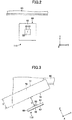
- Fig. 2 is a drawing illustrating the antenna in a front view.
- Fig. 3 is a drawing illustrating the antenna in a side view.
- the antenna 110 illustrated in Figs. 2, 3 is arranged at a position away from the interior-side surface 76 of the glass plate 70.
- the glass plate 70 includes the interior-side surface 76 at an interior side of the vehicle 80 and an exterior-side surface 77 at an exterior side of the vehicle 80.
- the interior-side surface 76 is the one of the surfaces of the glass plate 70.
- the exterior-side surface 77 is a surface on the opposite side from the one of the surfaces of the glass plate 70.
- the plate thickness T denotes the thickness of the glass plate 70, and is 1.1 mm or more as explained above.
- the distance D is the shortest distance between the interior-side surface 76 and the antenna 110.
- the distance D denotes the shortest distance between the radiation plate 20 and the interior-side surface 76.
- the antenna 110 is arranged away from the glass plate 70, and accordingly, the distance D is more than zero. In other words, when the distance D is zero, the antenna 110 is in contact with the interior-side surface 76. Note that the antenna 110 may be arranged parallel to or non-parallel to the interior-side surface 76, and even when the antenna 110 is arranged non-parallel, the distance D represents the shortest distance between the radiation plate 20 and the interior-side surface 76.
- the distance D may be the shortest distance between the radiation plate 20 and the interior-side surface 76 as described above.
- the radiation plate 20 is an example for radiating electromagnetic waves at a predetermined frequency of 10 GHz or more, and in the present specification, not only the radiation plate 20 but also a slot for radiating electromagnetic waves at approximately the same frequency are collectively referred to as a "radiation unit 20".
- An aspect in which the antenna 110 is located away from one of the surfaces of the glass plate 70 includes, as long as an adhesive member for bonding the antenna 110 with the one of the surfaces has a finite thickness, an aspect in which the adhesive member is interposed between the antenna 110 and the one of the surfaces. In this case, (the shortest distance of) the thickness of the adhesive member corresponds to the distance D.
- adhesive members include adhesive agents, pressure-sensitive adhesive agents, adhesive tapes, and the like.
- an aspect in which the antenna 110 is located away from one of the surfaces of the glass plate 70 includes an aspect in which the antenna 110 is in contact with the one of the surfaces via an interposing member such as an adhesive member and the like.
- adhesive members examples include acrylic resin, rubber, silicone resin, butadiene resin, epoxy resin, polyurethane resin, polyvinyl acetal resin, polyvinyl chloride resin, ionomer, polyester resin, ethylene-vinyl acetate copolymer resin, ethylene-ethyl acrylic copolymer resin, polycycloolefin resin, and the like. Among them, only one type may be used, or two or more types may be used in combination.
- a ratio of radiated electric power radiated from the antenna 110 to input electric power input into the antenna 110 is defined as a radiation efficiency.
- the input electric power input to the antenna 110 represents the electric power received by the antenna 110 from among the electric power fed to the antenna 110. Therefore, for example, the electric power lost in a transmission line such as a coaxial cable and a microstrip line connected to the antenna 110 is not included in the above "input electric power input to the antenna 110".
- the radiation efficiency is related to the plate thickness T and the distance D.
- an effective wavelength of electromagnetic waves at a predetermined frequency of 10 GHz or more is denoted as ⁇ g.
- the effective wavelength ⁇ g means a wavelength in view of a wavelength shortening rate (i.e., a velocity factor) of such a material.
- the matching layer and the spacer may be formed by a coating such as a dry coating or a wet coating.
- the inventors of the present application have found that, when the glass plate 70 and the antenna 110 are arranged to obtain a radiation efficiency ⁇ A [dB] satisfying " ⁇ A ⁇ ⁇ 0 + ( ⁇ ⁇ g/2 - ⁇ 0 ) ⁇ 0.1", electromagnetic waves at a radio frequency band of 10 GHz or more can be transmitted and received without processing the glass plate 70.
- the radiation efficiency ⁇ A satisfies " ⁇ A ⁇ ⁇ 0 + ( ⁇ ⁇ g/2 - ⁇ 0 ) ⁇ 0.2”, and more preferably satisfies " ⁇ A ⁇ ⁇ 0 + ( ⁇ ⁇ g/2 - ⁇ 0 ) ⁇ 0.3".
- without processing the glass plate 70 includes a case of not performing processing to partially reduce the thickness of the glass plate 70 in proximity to the antenna 110, and in normal circumstances, "without processing the glass plate 70" means that the state of the single glazing or the insulated glazing used is maintained.
- the inventors of the present application have found that, when the glass plate 70 and the antenna 110 are arranged to obtain a radiation efficiency ⁇ A of - 10 [dB] or more, electromagnetic waves at a radio frequency band of 10 GHz or more can be transmitted and received without processing the glass plate 70. Also, the inventors of the present application have found that, when the glass plate 70 and the antenna 110 are arranged to obtain a radiation efficiency ⁇ A of preferably -7 [dB] or more, more preferably -5 [dB] or more, still more preferably -3 [dB] or more, and yet still more preferably -1 [dB] or more, electromagnetic waves at a radio frequency band of 10 GHz or more can be transmitted and received without processing the glass plate 70.
- the antenna 110 as illustrated in Figs. 2, 3 includes at least the conductor plate 10 and the radiation plate 20.
- the conductor plate 10 is a planar layer of which the surface is parallel to the XY plane, and functions as the ground of the antenna 110.
- the conductor plate 10 is a plate-shaped or film-shaped conductor. Examples of materials of conductors used for the conductor plate 10 include silver, copper, and the like, but are not limited thereto.
- the shapes of the conductor plates 10 illustrated in the drawings are squares in a plan view (i.e., as seen in the Z axis direction), the shapes may also be polygonal shapes other than a square, and may be other shapes such as circular shapes.
- plate-shaped or “film-shaped” may include shapes having three-dimensional shapes such as, for example, a protruding shape, a recessed shape, a wavy shape, and the like. This is also applicable to a conductor plate and a dielectric substrate explained later.
- "plate-shaped” or “film-shaped” explained above is preferably a planar shape (two-dimensional shape) because predetermined antenna gain characteristics can be easily predicted.
- the radiation plate 20 is a plate-shaped or film-shaped conductor arranged to face the conductor plate 10 in the Z axis direction, and the size of area of the radiation plate 20 is smaller than the size of area of the conductor plate 10.
- the radiation plate 20 is a planar layer of which the surface is parallel to the XY plane, and functions as a radiating element of the antenna 110. Examples of materials of conductors used for the radiation plate 20 include silver, copper, and the like. However, the materials of the conductors are not limited thereto.
- the shapes of the radiation plates 20 illustrated in the drawings are squares in the plan views (i.e., as seen in the Z axis direction), the shapes may also be polygonal shapes other than a square, and may be other shapes such as circular shapes.
- the radiation plate 20 is arranged away from the conductor plate 10.
- the medium between the conductor plate 10 and the radiation plate 20 includes either a space or a dielectric substrate, or includes both of the space and the dielectric substrate.
- Figs. 2, 3 illustrate cases where the medium is constituted by only the dielectric substrate 60.
- the radiation plate 20 and the conductor plate 10 may be fixed by a housing, not illustrated, as necessary.
- the dielectric substrate 60 is a plate-shaped or film-shaped dielectric layer of which the main component is a dielectric.
- the dielectric substrate 60 includes a first surface 61 and a second surface 62 on a side opposite to the first surface 61.
- the surfaces 61, 62 are parallel to the XY plane.
- the radiation plate 20 is provided on the surface 61, i.e., one of the surfaces of the dielectric substrate 60.
- the conductor plate 10 is provided on the surface 62, i.e., the other of the surfaces of the dielectric substrate 60.
- the dielectric substrate 60 may be, for example, a dielectric substrate such as a glass epoxy substrate or a dielectric sheet.
- a dielectric substrate such as a glass epoxy substrate or a dielectric sheet.
- materials of dielectrics used for the dielectric substrate 60 include glass such as silica glass, ceramics, fluororesin such as polytetrafluoroethylene, liquid crystal polymer, cycloolefin polymer, and the like, but are not limited thereto.
- the dielectric substrate 60 is a resin material
- the surface of the resin may be coated with an ultraviolet absorbing layer, or an ultraviolet absorber may be added to the resin material in order to increase the ultraviolet resistance.
- the antenna 110 is, for example, a planar antenna arranged so as to be parallel to the interior-side surface 76.
- the antenna 110 i.e., the planar antenna
- the antenna 110 can be easily implemented with a low profile.
- the antenna 110 is a planar antenna including the dielectric substrate 60, the radiation plate 20 arranged on the first surface 61, and the conductor plate 10 on the opposite side of the dielectric substrate 60 from the radiation plate 20.
- the planar antenna having such a structure is referred to as a patch antenna or a microstrip antenna.
- Fig. 4 is a perspective view illustrating the antenna 110 including the dielectric substrate 60 formed with the conductor plate 10 and the radiation plate 20.
- Fig. 5 is a cross-sectional view illustrating the antenna 110 including the dielectric substrate 60 formed with the conductor plate 10 and the radiation plate 20.
- the antenna 110 includes a connection conductor 40 connecting the feeding portion 30 and the radiation plate 20 so as to penetrate a portion of the dielectric substrate 60.
- the feeding portion 30 is a portion to be fed with or without contact, and is a portion that is brought into contact with or arranged in proximity to one end of a transmission line (not illustrated).
- a transmission line include a coaxial cable and a microstrip line.
- the other end of the transmission line is connected to a communication apparatus for communicating with the outside of the vehicle using the antenna 110.
- the feeding portion 30 is located on the same side as the conductor plate 10 with respect to the radiation plate 20.
- connection conductor 40 is not in contact with the conductor plate 10.
- One end of the connection conductor 40 is connected to the feeding portion 30, and the other end is connected to the radiation plate 20 at a connection point 22.
- the connection point 22 is shifted from a center of gravity 21 of the radiation plate 20.
- the connection point 22 is located on the negative side of the Y axis direction with respect to the center of gravity 21.
- the center of gravity 21 corresponds to the center of a symmetric figure when the radiation plate 20 has a symmetric figure such as a square.
- connection conductor 40 examples include a conductor formed in a through hole penetrating the dielectric substrate 60 in the Z axis direction, a core wire of a coaxial cable, and a conductor pin formed in a pin shape, but the connection conductor 40 is not limited thereto.
- the connection conductor 40 include a core wire of a coaxial cable and a conductor pin, but the connection conductor 40 is not limited thereto.
- the center of gravity 21 of the radiation plate 20 preferably overlaps with a center of gravity 11 of the conductor plate 10 as seen from a viewpoint on the side of the radiation plate 20 with respect to the conductor plate 10, in order to improve the antenna gain of the antenna 110 in the direction from the conductor plate 10 to the radiation plate 20.
- the viewpoint on the side of the radiation plate 20 with respect to the conductor plate 10 means a view point as seen from the positive side of the Z axis direction
- the direction from the conductor plate 10 to the radiation plate 20 means a direction toward the positive side of the Z axis direction.
- the coaxial cable and the microstrip line have been explained as examples of the transmission line to the planar antenna, but hereinafter the transmission line is explained in a more specific manner.
- the planar antenna and the transmission line are collectively referred to as a "transmission line-attached antenna".
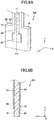
- Fig. 6A is a perspective view illustrating a transmission line-attached antenna 201
- Fig. 6B is a cross-sectional view taken along Y1-Y1'.
- the transmission line-attached antenna 201 includes a dielectric substrate 60, a radiation plate 20 arranged on a first surface 61 of the dielectric substrate 60, and a microstrip line 24 arranged on the first surface 61 and connected to the radiation plate 20.
- the transmission line-attached antenna 201 includes a conductor plate 10 on a second surface 62 on the opposite side of the dielectric substrate 60 from the first surface 61, and functions as a ground.
- the dielectric loss tangent (tan ⁇ ) of the dielectric substrate 60 may be 0.03 or less, more preferably 0.008 or less, and still more preferably 0.001 or less.
- the transmission loss from the transmission line can be reduced more greatly, and accordingly, the transmission loss of the microstrip line 24 can be reduced more greatly.
- the effect of reducing the transmission loss is likely to become more significant.
- a configuration having a matching layer 74 or having both of the matching layer 74 and a spacer 75 between the radiation plate 20 (i.e., the antenna 110) and the glass plate 70 as explained later with reference to Fig. 12 to Fig.
- the transmission loss of the microstrip line 24 can be reduced more greatly when the thickness of the dielectric substrate 60 is thinner.
- the thickness of the dielectric substrate 60 may be 0.1 ⁇ ⁇ 0 or less, more preferably 0.08 ⁇ ⁇ 0 or less, and still more preferably 0.06 ⁇ ⁇ 0 or less.
- the lower limit of the thickness of the dielectric substrate 60 is not particularly limited, the lower limit may be 0.01 mm or more for the ease of handling.
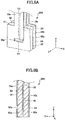
- Fig. 7A is a perspective view illustrating a transmission line-attached antenna 202.
- Fig. 7B is a cross-sectional view taken along Y2-Y2'.
- the transmission line-attached antenna 202 includes a first dielectric substrate 60a, a second dielectric substrate 60b, a radiation plate 20, a conductor plate 10, a connection conductor 40, and a microstrip line 25.
- the first dielectric substrate 60a and the second dielectric substrate 60b are arranged to overlap with each other in the thickness direction.
- the first dielectric substrate 60a includes a first surface 61 on the opposite side from the second dielectric substrate 60b and a second surface 62 on the same side as the second dielectric substrate 60b.
- the second dielectric substrate 60b includes a third surface 63 on the same side as the first dielectric substrate 60a and a fourth surface 64 on the opposite side from the first dielectric substrate 60a.
- the first dielectric substrate 60a and the second dielectric substrate 60b may be made of different materials or may be made of the same material.
- the transmission line-attached antenna 202 includes a radiation plate 20 arranged on the first surface 61, a connection conductor 40 connected to the radiation plate 20, and a microstrip line 25 connected to the connection conductor 40.
- the transmission line-attached antenna 202 includes, between the first dielectric substrate 60a and the second dielectric substrate 60b, a conductor plate 10 on the second surface 62 and the third surface 63.
- the conductor plate 10 functions as a ground.
- the connection conductor 40 is a conductor that extends in the thickness direction (i.e., the Z axis direction) of the first dielectric substrate 60a and the second dielectric substrate 60b to be formed in a through hole penetrating the first dielectric substrate 60a, the conductor plate 10, and the second dielectric substrate 60b.
- the connection conductor 40 is not connected to at least the conductor plate 10.
- the microstrip line 25 is provided on the fourth surface 64.
- the microstrip line 25 is provided on the opposite side of the conductor plate 10 from the radiation plate 20 (i.e., on the minus side of the Z axis direction). Therefore, the transmission line-attached antenna 202 can reduce the transmission loss of the microstrip line 25 caused by a dielectric, not illustrated, provided between the radiation plate 20 and the glass plate 70 or caused by the glass plate 70.
- Fig. 8A is a perspective view illustrating a transmission line-attached antenna 203.
- Fig. 8B is a cross-sectional view taken along Y3-Y3'.
- the transmission line-attached antenna 203 includes a first dielectric substrate 60a, a second dielectric substrate 60b, a slot 20a, a first conductor plate 10a, a second conductor plate 10b, and a strip line 26.
- the first dielectric substrate 60a and the second dielectric substrate 60b are arranged to overlap with each other in the thickness direction.
- the first dielectric substrate 60a includes a first surface 61 on the opposite side from the second dielectric substrate 60b and a second surface 62 on the same side as the second dielectric substrate 60b.
- the second dielectric substrate 60b includes a third surface 63 on the same side as the first dielectric substrate 60a and a fourth surface 64 on the opposite side from the first dielectric substrate 60a.
- the first dielectric substrate 60a and the second dielectric substrate 60b may be made of different materials or may be made of the same material.
- a slot 20a corresponds to the "radiation unit 20".
- the transmission line-attached antenna 203 includes a strip line 26 provided between the second surface 62 and the third surface 63.
- the transmission line-attached antenna 203 includes a first conductor plate 10a on a first surface 61, so that the first conductor plate 10a overlaps with at least a portion of the strip line 26 as seen from the thickness direction (i.e., the Z axis direction) of the first dielectric substrate 60a and the second dielectric substrate 60b.
- the first conductor plate 10a functions as a ground.
- the transmission line-attached antenna 203 is a what is termed as a slot antenna that has the slot 20a formed with an opening in a portion of the first conductor plate 10a.
- the slot 20a preferably overlaps with at least a portion of the strip line 26 (for example, an end portion).
- the slot 20a may be formed by a concave portion in which the first surface 61 is exposed, and in this case, the medium of the concave portion forming the slot 20a is air, but the concave portion may be filled with a dielectric material other than air.
- the transmission line-attached antenna 203 includes a second conductor plate 10b on the fourth surface 64, so that the second conductor plate 10b overlaps with the slot 20a and the strip line 26, as seen in the thickness direction (i.e., the Z axis direction) of the first dielectric substrate 60a and the second dielectric substrate 60b.
- the second conductor plate 10b functions as a ground.
- the strip line 26 is arranged between the first conductor plate 10a and the second conductor plate 10b as seen in the Z axis direction. Therefore, the transmission line-attached antenna 203 can reduce the transmission loss of the strip line 26 caused by a dielectric, not illustrated, provided between the first conductor plate 10a and the glass plate 70 and caused by the glass plate 70.
- Fig. 9A is a perspective view illustrating a transmission line-attached antenna 204.
- Fig. 9B is a cross-sectional view taken along Y4-Y4'.
- Fig. 9C is a cross-sectional view taken along Y5-Y5'.
- the transmission line-attached antenna 204 is configured such that a transmission line of a signal functions as a substrate integrated waveguide (SIW).
- the transmission line-attached antenna 204 includes a first surface 61 and a (first) dielectric substrate 60a opposite to the first surface 61, a first conductor plate 27a arranged on the first surface 61, and a second conductor plate 27b arranged on the second surface 62.
- the transmission line-attached antenna 204 is a what is termed as a slot antenna that has a slot 20a formed with an opening in a portion of the first conductor plate 27a.
- the concave portion of the slot 20a may be filled with air or a dielectric material other than air.
- the transmission line-attached antenna 204 includes conductor walls 28a, 28b, 28c that extend in the thickness direction of the dielectric substrate 60a and that are made of conductor materials to connect the first conductor plate 27a and the second conductor plate 27b.
- the transmission line-attached antenna 204 as illustrated in Fig. 9A includes (a plurality of) conductor walls 28a arranged with regular intervals in the Y axis direction, (a plurality of) conductor walls 28b arranged substantially parallel to the (plurality of) conductor walls 28a, and (a plurality of) conductor walls 28c arranged with regular intervals in the X axis direction so as to surround the slot 20a.
- the transmission line corresponds to the dielectric substrate 60a located between (the plurality of) conductor walls 28a, (the plurality of) conductor walls 28b, and (the plurality of) conductor walls 28c.
- the conductor walls 28a, the conductor walls 28b, and the conductor walls 28c are collectively referred to as "conductor walls 28".
- the conductor walls 28 are arranged in a U shape so as to surround the slot 20a as seen in the thickness direction of the dielectric substrate 60a (i.e., the Z axis direction).
- the transmission line-attached antenna 204 includes conductor plates (i.e., the first conductor plate 27a and the second conductor plate 27b) arranged on both of the principal surfaces of the dielectric substrate 60a and the conductor walls 28 connecting both of the conductor plates in the thickness direction of the dielectric substrate 60a. Because the conductor plates (i.e., the first conductor plate 27a and the second conductor plate 27b) and the conductor walls 28 are provided, the transmission loss of the transmission line provided in the dielectric substrate 60a caused by a dielectric, not illustrated, provided between the first conductor plate 27a and the glass plate 70 and caused by the glass plate 70 can be reduced.
- conductor plates i.e., the first conductor plate 27a and the second conductor plate 27b
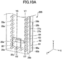
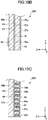
- Fig. 10A is a perspective view illustrating a transmission line-attached antenna 205.
- Fig. 10B is a cross-sectional view taken along Y6-Y6'.
- Fig. 10C is a cross-sectional view taken along Y7-Y7'.
- the transmission line-attached antenna 205 includes additional elements in addition to the transmission line-attached antenna 204, and explanation about features similar to the explanation about the transmission line-attached antenna 204 is omitted.
- the transmission line-attached antenna 205 includes, as the additional elements, a second dielectric substrate 60b and a slot 20a.
- the first dielectric substrate 60a and the second dielectric substrate 60b are arranged to overlap with each other in the thickness direction.
- the first dielectric substrate 60a includes a first surface 61 on the same side as the second dielectric substrate 60b and a second surface 62 on the opposite side from the second dielectric substrate 60b.
- the second dielectric substrate 60b includes a third surface 63 on the opposite side from the first dielectric substrate 60a and a fourth surface 64 on the same side as the first dielectric substrate 60a.
- the first dielectric substrate 60a and the second dielectric substrate 60b may be made of different materials or may be made of the same material.
- the second dielectric substrate 60b includes a radiation plate 20 on the third surface 63, and includes a first conductor plate 27a on the fourth surface 64.
- the radiation plate 20 is arranged at a position close to the slot 20a as seen in the thickness direction of the first dielectric substrate 60a and the second dielectric substrate (i.e., the Z axis direction).
- the transmission line-attached antenna 205 includes: the conductor plates (i.e., the first conductor plate 27a and the second conductor plate 27b) on both of the principal surfaces of the first dielectric substrate 60a; and the conductor walls 28 connecting both of the conductor plates in the thickness direction of the first dielectric substrate 60a.
- the conductor plates i.e., the first conductor plate 27a and the second conductor plate 27b
- the conductor walls 28 are provided, the transmission loss of the transmission line provided in the first dielectric substrate 60a caused by a dielectric, not illustrated, provided between the radiation plate 20 and the glass plate 70 and caused by the glass plate 70 can be reduced.
- the radiation unit corresponds to the radiation plate 20.
- transmission lines include a coplanar line, a conductor back coplanar wave guide (CBCPW), a post wall waveguide (PWW), a coplanar strip (CPS), and a slot line.
- CBCPW conductor back coplanar wave guide
- PWW post wall waveguide
- CPS coplanar strip
- Fig. 11 is a partial cross-sectional view of an example of an antenna for a vehicle system having multiple antennas (transmission line-attached antennas) .
- An antenna system 100 as illustrated in Fig. 11 includes a windshield 71, a rear window glass 72, a front antenna 111 attached to the windshield 71, and a rear antenna 112 attached to the rear window glass 72.
- the windshield 71 and the rear window glass 72 are examples of the glass plate 70 explained above.
- the front antenna 111 and the rear antenna 112 are examples of the antenna 110 explained above.
- the front antenna 111 is an example of the first antenna.
- the rear antenna 112 is an example of the second antenna.
- the radiation plate 20 of the front antenna 111 is arranged at a predetermined inclination angle ⁇ with respect to a vertical plane 91 perpendicular to the horizontal plane 90. Even in that case, by adjusting the inclination angle ⁇ so that the radiation plate 20 is parallel to the interior-side surface of the windshield 71, the front antenna 111 can be easily implemented with a low profile.
- the radiation plate 20 of the rear antenna 112 is arranged at a predetermined inclination angle with respect to the vertical plane 91 perpendicular to the horizontal plane 90. Even in that case, by adjusting the inclination angle ⁇ so that the radiation plate 20 is parallel to the interior-side surface of the rear window glass 72, the rear antenna 112 can be easily implemented with a low profile.
- the front antenna 111 is arranged away from one of the surfaces of the windshield 71 so that the radiation plate 20 is located on the vehicle front-side with respect to the conductor plate 10.
- the rear antenna 112 is arranged away from one of the surfaces of the rear window glass 72 so that the radiation plate 20 is located on the vehicle rear-side with respect to the conductor plate 10.
- the front antenna 111 and the rear antenna 112 are attached in this manner, so that the front antenna 111 can ensure the antenna gain in the range in front of the vehicle, the rear antenna 112 can ensure the antenna gain in the range at the rear of the vehicle. Therefore, the antenna gain in the longitudinal direction of the vehicle 80 can be ensured.
- the conductor plate 10 of the front antenna 111 is arranged at a predetermined inclination angle ⁇ with respect to the vertical plane 91 perpendicular to the horizontal plane 90. Even in that case, by adjusting the inclination angle ⁇ so that the conductor plate 10 is parallel to the interior-side surface of the windshield 71, the front antenna 111 can be easily implemented with a low profile. This is also applicable to the inclination angle ⁇ of the conductor plate 10 of the rear antenna 112.
- “Arranging with an inclination of 0 degrees with respect to the vertical plane 91” means arranging parallel to the vertical plane 91.
- the antenna for the vehicle i.e., the transmission line-attached antenna
- the antenna 100 for the vehicle system may include: at least two window glasses selected from the windshield 71, the rear window glass 72, and the side window glass 73; and at least one antenna for the vehicle (i.e., the transmission line-attached antenna) attached to each of the at least two window glasses.
- the antenna system 100 may include multiple antennas on the windshield 71, and may include multiple antennas (i.e., transmission line-attached antennas) on the rear window glass 72.
- Fig. 12 is an arrangement drawing (i.e., a cross-sectional schematic view in the YZ plane) illustrating a configuration in which a matching layer 74 and air 92 are present between the glass plate 70 and the antenna 110.
- the matching layer 74 matches the impedance, so that the transmittance of the electromagnetic waves being transmitted through the glass plate 70 and the matching layer 74 can be improved.
- the matching layer 74 is in contact with one of the surfaces of the glass plate 70.
- the matching layer 74 is not limited to being in contact with the interior-side surface of the glass plate 70 with an adhesive agent, and the matching layer 74 may be configured to be in contact with the interior-side surface of the glass plate 70 via an attachment member such as a bracket and the like, not illustrated, without any adhesive agent.
- the matching layer 74 has a certain thickness, i.e., a rectangular shape, but the matching layer 74 is not limited thereto.
- the cross section of the matching layer 74 may be in a shape of a triangle, a trapezoid, or the like, with a surface that is not parallel to the interior-side surface 76 of the glass plate 70 or the antenna 110.
- the matching layer 74 may be a dielectric lens in a shape of plano-convex, plano-concave, or the like.
- the matching layer 74 has a distribution in the thickness, so that the directivity of the antenna can be adjusted according to desired specifications.
- the aspect of the matching layer 74 with a distribution in the thickness is not limited to Fig. 12 , and can also be applied to the explanations of Fig. 13 and Fig. 14 described later.
- the matching layer 74 may be configured to have an area in which the outer edge of the matching layer 74 is outside of the outer edge of the radiation unit 20 (i.e., the radiation plate 20 or the slot 20a). This is because electromagnetic waves from the radiation unit (i.e., the radiation plate 20 or the slot 20a) are radiated not only in the thickness direction (i.e., the Z axis direction) of the matching layer 74 but also with a predetermined spread angle with respect to the thickness direction, and accordingly, the effects of the matching layer 74 are also achieved in the direction of the electromagnetic waves radiated with such an angle. Further, in the plan view of the glass plate 70, the matching layer 74 may have an area in which the outer edge of the matching layer 74 is outside of the outer edge of the antenna 110.
- the material of the matching layer 74 is not particularly limited, and may be made of an organic material such as resin and an inorganic material such as glass.
- the matching layer 74 may be polyethylene terephthalate (PET) resin, cycloolefin resin (COP), acrylic resin, ABS resin, polycarbonate resin, vinyl chloride resin, and the like.
- PET polyethylene terephthalate
- COP cycloolefin resin
- acrylic resin acrylic resin
- ABS resin polycarbonate resin
- vinyl chloride resin vinyl chloride resin
- the matching layer 74 may be preferably made of cycloolefin resin due to its heat resistance.
- the surface of the resin may be coated with an ultraviolet absorbing layer, or an ultraviolet absorber may be added to the resin material in order to increase the ultraviolet resistance.
- the dielectric loss tangent (tan ⁇ ) of the matching layer 74 is preferably 0.03 or less, so that the gain of the antenna 110 can be improved as compared with the case where the dielectric loss tangent (tan ⁇ ) is more than 0.03.
- the dielectric loss tangent (tan ⁇ ) of the matching layer 74 is more preferably 0.02 or less, and still more preferably 0.01 or less, in order to improve the gain of the antenna 110.
- the lower limit value of the dielectric loss tangent (tan5) of the matching layer 74 may be more than zero (i.e., the dielectric loss tangent (tan ⁇ ) of air) .
- the matching layer 74 is not limited to be formed with only a dielectric, and may include a meta-material in which a plurality of metal patterns are coated with resin or the like, and the matching layer 74 itself may be composed of the meta-material.
- the meta-material can be designed to attain a dielectric constant and a magnetic permeability for a specific wavelength, and by applying this feature, the directivity of the antenna 110 can be adjusted to desired specifications.
- the matching layer 74 contains a dielectric and a meta-material
- the meta-material may be provided on the interior-side surface 76 of the glass plate 70 with respect to the dielectric, or may be provided on the side of the antenna 110 with respect to the dielectric. In a case where the spacer 75 explained below is provided, the meta-material may be arranged on the surface of the spacer 75.
- the meta-material may have a configuration capable of active control for changing the dielectric constant of the metal pattern by using an electric control circuit.
- the meta-material can adjust the directivity of the antenna 110 to a desired state according to the situation.
- the matching layer 74 is not limited to be formed with only the dielectric, and may include a director. With the director controlling the phase of electromagnetic waves, the directivity of the antenna 110 can be adjusted.
- the matching layer 74 is not limited to be formed with only the dielectric, and may include a frequency selective surface (FSS) constituted by a conductor (metal) pattern.
- FSS frequency selective surface
- the matching layer 74 itself may be constituted by a frequency selective surface.
- the frequency selective surface has openings (that do not have conductors) on the conductor surface, and can selectively transmit electromagnetic waves at a predetermined frequency with the pattern of the openings, so that a particular frequency transmitted and received by the antenna 110 can be selected more suitably for a desired range.
- the frequency selective surface may be provided on the interior-side surface 76 of the glass plate 70 with respect to the dielectric, or may be provided on the side of the antenna 110 with respect to the dielectric.
- the frequency selective surface may be arranged on the surface of the spacer 75. The frequency selective surface matches the impedance, so that the transmittance of the electromagnetic waves being transmitted through the glass plate 70 and the matching layer 74 can be improved.
- Fig. 13 is an arrangement drawing illustrating a configuration in which the matching layer 74 is present between the glass plate 70 and the antenna 110.
- air is not present between the glass plate 70 and the antenna 110.
- the matching layer 74 includes a first matching surface in contact with one of the surfaces of the glass plate 70 and a second matching surface in contact with the antenna 110.
- a preferable range of the dielectric loss tangent of the matching layer 74 is the same as described above.
- the matching layer 74 and the antenna 110 are illustrated as the same area, but due to a reason similar to the reason explained with reference to Fig.
- the matching layer 74 may have an area in which the outer edge of the matching layer 74 is outside of the outer edge of the radiation unit 20 (i.e., the radiation plate 20 or the slot 20a). Further, in the plan view, the matching layer 74 may have an area in which the outer edge of the matching layer 74 is outside of the outer edge of the antenna 110.
- Fig. 14 is an arrangement drawing illustrating a configuration in which the matching layer 74 and the spacer 75 are provided between the glass plate 70 and the antenna 110.
- air is not present between the glass plate 70 and the antenna 110, but air may be present between the glass plate 70 and the antenna 110.
- the matching layer 74 may not be provided.
- the matching layer 74 includes a first matching surface in contact with one of the surfaces of the glass plate 70 and a second matching surface in contact with the spacer 75.
- a preferable range of the dielectric loss tangent of the matching layer 74 is the same as described above.
- the spacer 75 is a distance adjustment member for adjusting the distance from the glass plate 70 to the antenna 110.
- the spacer 75 not only has a shape for adjusting the distance, but also can achieve a function similar to the matching layer by using a material capable of adjusting the impedance.
- the spacer 75 illustrated in Fig. 14 includes a first spacer surface in contact with the matching layer 74 and a second spacer surface in contact with the antenna 110.
- the spacer 75 is not limited to the spacer illustrated in Fig. 14 , and may have, for example, a tubular structure having a predetermined thickness of a peripheral wall and formed with a through hole in the center.
- the spacer 75 and the matching layer 74 preferably have an area in which the outer edge of the spacer 75 and of the matching layer 74 is outside of the radiation unit (i.e., the radiation plate 20 or the slot 20a).
- electromagnetic waves from (the radiation plate 20 of) the antenna 110 are radiated not only in the thickness direction (i.e., the Z axis direction) of the spacer 75 and the matching layer 74 but also with a predetermined spread angle with respect to the thickness direction.
- the spacer 75 and the matching layer 74 may be configured to have an area in which the outer edge of the spacer 75 and of the matching layer 74 is outside of the outer edge of the antenna 110.
- the dielectric loss tangent (tan ⁇ ) of the spacer 75 is preferably 0.03 or less, so that the gain of the antenna 110 can be improved as compared with the case where the dielectric loss tangent (tan ⁇ ) is more than 0.03.
- the dielectric loss tangent (tan5) of the spacer 75 is more preferably 0.02 or less, and is still more preferably 0.01 or less.
- the lower limit value of the dielectric loss tangent (tan ⁇ ) of the spacer 75 may be more than zero (i.e., the dielectric loss tangent (tan ⁇ ) of air).
- the material of the spacer 75 is not particularly limited, and in a manner similar to the matching layer 74 explained above, the material of the spacer 75 may be made of an organic material such as resin and an inorganic material such as glass.
- the spacer 75 is a resin material, in a manner similar to the matching layer 74, the surface of the resin may be coated with an ultraviolet absorbing layer, or an ultraviolet absorber may be added to the resin material in order to increase the ultraviolet resistance.
- the antenna 110 can be easily designed as compared with the case where the relative dielectric constant of the spacer 75 is more than the relative dielectric constant of the glass plate 70.
- the relative dielectric constant of the glass plate 70 is 5 or more and is 9 or less, and accordingly, the relative dielectric constant of the spacer 75 is preferably 1.5 or more and 7 or less, and more preferably 2 or more and 5 or less.
- the relative dielectric constant is a value at a frequency of 28 GHz.
- Fig. 15 is a drawing illustrating an example of an antenna system having an array antenna.
- An antenna i.e., a transmission line-attached antenna located away from one of the surfaces of the glass plate 70 may be an array antenna in which a plurality of antenna elements are arranged.
- Fig. 15 illustrates an array antenna 113 in which four antenna elements 20A, 20B, 20C, and 20D are arranged in the Y axis direction.
- the array antenna 113 includes multiple antennas, in an array form, having a configuration similar to the configuration of the antenna 110 explained above.
- Each of the antenna elements 20A, 20B, 20C, and 20D has a configuration similar to the radiation plate 20 or the slot 20a explained above.
- Each of the feeding portions 30A, 30B, 30C, and 30D has a configuration similar to the feeding portion 30 explained above.
- the antenna i.e., the transmission line-attached antenna located away from one of the surfaces of the glass plate 70 is the array antenna in which the plurality of antenna elements are arranged, the radiation range of the antenna (the directivity of the antenna) can be expanded.
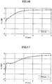
- Figs. 16 to 19 are graphs illustrating examples of changes in the radiation efficiency ⁇ A of electromagnetic waves at 28 GHz according to the distance D between the antenna 110 and the glass plate 70, when the plate thickness T of the glass plate 70 was 2, 3, 4, 5 mm, respectively.
- Figs. 16 to 19 illustrate data measured by a simulation.
- the medium constituting the distance D was air.
- the sizes of respective portions of the antenna 110 illustrated in Fig. 4 were as follows, in units of millimeters. L60 : 10 L61 : 10 L62 : 0.2 L20 : 2.6 L21 : 2.6
- the shortest distance from the connection point 22 to one side of the radiation plate 20 in the square shape was 0.9 mm.
- the relative dielectric constant of the dielectric substrate 60 for electromagnetic waves at 28 GHz was 3.79.
- the shape of the glass plate 70 was a square with a length of 50 mm and a width of 50 mm.
- the glass plate 70 had a relative dielectric constant of 6.8 and a dielectric loss tangent of 0.01.
- the simulation was performed under a condition that the surface of the radiation plate 20 and the interior-side surface of the glass plate 70 were arranged parallel to each other, and at any position, the distance therebetween was the distance D.
- Figs. 16 to 19 As shown in Figs. 16 to 19 , as the distance D decreases, the radiation efficiency ⁇ A tends to decrease. When compared with the same distance D, the radiation efficiency ⁇ A decreases more greatly as the plate thickness T increases.
- the measurement data shown in Figs. 16 to 19 indicates that radiation efficiencies ⁇ A satisfying " ⁇ A ⁇ ⁇ 0 + ( ⁇ ⁇ g/2 - ⁇ 0 ) ⁇ 0.1" explained above have been attained.
- Fig. 16 to Fig. 19 illustrate characteristics of electromagnetic waves at the frequency of 28 GHz, the wavelength decreases as the frequency increases, and accordingly, the value of the distance D satisfying " ⁇ A ⁇ ⁇ 0 + ( ⁇ ⁇ g/2 - ⁇ 0 ) ⁇ 0.1" decreases. In other words, when the frequency of the electromagnetic waves transmitted and received is high, the distance D can be reduced, and accordingly, the antenna 110 can be brought closer to the glass plate 70, and the antenna system can be easily implemented with a low profile.
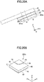
- Fig. 20A illustrates a configuration in which a transmission line-attached antenna 201 is attached to a glass plate 70 via a matching layer 74, and includes a first adhesive member 51 connecting the transmission line-attached antenna 201 and the matching layer 74 and a second adhesive member 52 connecting the glass plate 70 and the matching layer 74.
- Fig. 20A illustrates a configuration in which a transmission line-attached antenna 201 is attached to a glass plate 70 via a matching layer 74, and includes a first adhesive member 51 connecting the transmission line-attached antenna 201 and the matching layer 74 and a second adhesive member 52 connecting the glass plate 70 and the matching layer 74.
- the transmission line-attached antenna 201 includes an antenna area 201a included in the area A and a transmission line area 201b included in the area B.
- Fig. 20B is a perspective view illustrating only the transmission line area 201b of the transmission line-attached antenna 201 from among the area B.
- the transmission line area 201b includes a dielectric substrate 60, a microstrip line 24 serving as a transmission line on the first surface 61 of the dielectric substrate 60, and a conductor plate 10 provided on the second surface 62 to function as a ground.
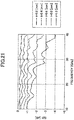
- the transmission characteristic (S21) of the transmission line with respect to the frequency was simulated under the same condition except that the thickness (t) of the dielectric substrate 60 was changed in the area B, i.e., the structure in which the transmission line area 201b of the transmission line-attached antenna 201, the first adhesive member 51, the matching layer 74, the second adhesive member 52, and the glass plate 70 are stacked in this order.
- the thickness (t) of the dielectric substrate 60 was changed to 0.2 mm (0.027 ⁇ ⁇ 0'), 0.4 mm (0.053 ⁇ ⁇ 0'), 0.6 mm (0.080 ⁇ ⁇ 0'), 0.8 mm (0.11 ⁇ ⁇ 0'), and 1.0 mm (0.13 ⁇ ⁇ 0').
- ⁇ 0' denotes a wavelength (approximately 7.5 mm) in a vacuum at 40 GHz.
- the conditions of this simulation were as follows. [Table 1] Thickness [mm] Relative dielectric constant Glass plate 70 3.0 6.8 Second adhesive member 52 0.5 2.5 Matching layer 74 5.0 3.0 First adhesive member 51 0.5 2.5 Dielectric substrate 60 0.2 to 1.0 3.79
- the simulation was performed while the matching layer 74 was assumed to be a cycloolefin polymer (COP) and the dielectric substrate 60 was assumed to be synthetic fused silica glass (manufactured by AGC Inc. under the tradename of "AQ Series") .
- the transmission line area 201b as illustrated in Fig. 20B was in a quadrangular shape with a size of 10 mm by 10 mm in the XY plane.
- the microstrip line 24 had a width of 0.25 mm, and included a straight line with a length of 3.5 mm in parallel to the X axis direction, a straight line with a length of 3.5 mm in parallel to the Y axis direction, and a straight line connecting these two straight lines and having a length of 2.1 mm at an angle of 45 degrees with respect to the X axis and the Y axis.
- the microstrip line 24 was a line the entire length of which was about 9.1 mm and which had two bending points bent by 135 degrees in the XY plane.
- Fig. 21 is a graph showing transmission losses (S21 in units of [dB]) that occur in the microstrip line 24 in the laminate referred to as the area B when signals were transmitted between both ends of the microstrip line 24 of Fig. 20B , i.e., in a path from a point P1 to a point P2.
- the transmission loss the value of S21
- the characteristic S21 for the frequency of 10 GHz or more becomes more stable (the fluctuation decreases).
- the glass plate is not limited to a glass plate for a vehicle, and may be glass plates for buildings or electronic devices.
Landscapes
- Physics & Mathematics (AREA)
- Electromagnetism (AREA)
- Engineering & Computer Science (AREA)
- Computer Security & Cryptography (AREA)
- Radar, Positioning & Navigation (AREA)
- Remote Sensing (AREA)
- Waveguide Aerials (AREA)
- Variable-Direction Aerials And Aerial Arrays (AREA)
- Support Of Aerials (AREA)
- Details Of Aerials (AREA)
Abstract
Description
- The present invention relates to an antenna system.
- In recent years, there is an ongoing trend of expansion of services using high-speed and large-capacity wireless communication systems communicating in microwave and millimeter wave frequency bands, such as a trend of transition from 4G LTE to 5G (sub6). Specifically, the bandwidth used for such services tends to expand from the 3 GHz band to the 5 to 6 GHz band. An antenna that can support such frequency bands with a high directivity and a high reception sensitivity is desired. V2X (Vehicle to Everything), which is expected to be used as vehicle-to-vehicle communication and road-to-vehicle communication, has been developed for various purposes such as, e.g., an electronic toll collection (ETC) system in 5.9 GHz band in Europe. In addition, attempts have been made to spread wireless communication systems that use frequencies higher than sub6 (for example, 28 GHz band, 40 GHz band, 60 GHz band, and 70 GHz band).
- In order to perform such high frequency band communication, for example, when a millimeter wave radar mounted on a car performs transmission and reception, an attenuation in the gain may occur due to window glass, which does not occur significantly with conventional frequency band communication. Therefore, in order to obtain a higher gain, a configuration in which an electromagnetic wave transmitting material is embedded in a portion of a window glass is disclosed (see for example, PTL 1).
- PTL 1: International Publication No.
2017/188415 - However, the technique of
PTL 1 has a problem in that the configuration becomes complicated because the window glass itself is mechanically processed and a member other than the window glass is included in a portion where the window glass is normally present. - In view of the above, the present disclosure provides an antenna system that transmits and receives electromagnetic waves in a predetermined radio frequency band with the use of a conventional glass plate with a thickness of 1.1 mm or more and a dielectric loss tangent of 0.005 or more at 28 GHz without complicating the configuration of the glass plate.
- The present disclosure provides an antenna system including:
- a glass plate having a thickness of 1.1 mm or more and having a dielectric loss tangent of 0.005 or more at 28 GHz; and
- an antenna located away from one of surfaces of the glass plate,
- wherein a ratio of electric power radiated from the antenna to electric power input into the antenna is defined as a radiation efficiency, and
- wherein where an effective wavelength of an electromagnetic wave at a predetermined frequency that is 10 GHz or more is denoted as λg, and where the radiation efficiency is denoted as η0 [dB] when the glass plate and the antenna are in contact with each other, and is denoted as ηλg/2 [dB] when a distance between the one of the surfaces and the antenna is λg/2, the glass plate and the antenna are arranged so as to obtain the radiation efficiency of ηA [dB] that satisfies ηA ≥ η0 + (ηλg/2 - η0) × 0.1.
- According to the technique of the present disclosure, an antenna system can be provided that transmits and receives electromagnetic waves in a predetermined radio frequency band with the use of a conventional glass plate with a thickness of 1.1 mm or more and a dielectric loss tangent of 0.005 or more at 28 GHz without complicating the configuration of the glass plate.
-
-
FIG. 1 is a perspective view illustrating an antenna system; -
Fig. 2 is a front view of an antenna; -
Fig. 3 is a side view of an antenna; -
Fig. 4 is a perspective view of an antenna; -
Fig. 5 is a cross-sectional view of an antenna; -
Fig. 6A is a perspective view of a transmission line-attached antenna; -
Fig. 6B is a cross-sectional view of a transmission line-attached antenna; -
Fig. 7A is a perspective view of a transmission line-attached antenna; -
Fig. 7B is a cross-sectional view of a transmission line-attached antenna; -
Fig. 8A is a perspective view of a transmission line-attached antenna; -
Fig. 8B is a cross-sectional view of a transmission line-attached antenna; -
Fig. 9A is a perspective view of a transmission line-attached antenna; -
Fig. 9B is a cross-sectional view of a transmission line-attached antenna; -
Fig. 9C is a cross-sectional view of a transmission line-attached antenna; -
Fig. 10A is a perspective view of a transmission line-attached antenna; -
Fig. 10B is a cross-sectional view of a transmission line-attached antenna; -
Fig. 10C is a cross-sectional view of a transmission line-attached antenna; -
Fig. 11 is a drawing illustrating an example of an antenna system including a plurality of antennas; -
Fig. 12 is an arrangement drawing illustrating a configuration in which a matching layer and air are present between a glass plate and an antenna; -
Fig. 13 is an arrangement drawing illustrating a configuration in which a matching layer is present between the glass plate and the antenna; -
Fig. 14 is an arrangement drawing illustrating a configuration in which a matching layer and a spacer are present between the glass plate and the antenna; -
Fig. 15 is a drawing illustrating an example of an antenna system having an array antenna; -
Fig. 16 is a graph illustrating an example of a change in a radiation efficiency according to a distance between an antenna and a glass plate with a plate thickness of 2 mm; -
Fig. 17 is a graph illustrating an example of a change in a radiation efficiency according to a distance between an antenna and a glass plate with a plate thickness of 3 mm; -
Fig. 18 is a graph illustrating an example of a change in a radiation efficiency according to a distance between an antenna and a glass plate with a plate thickness of 4 mm; -
Fig. 19 is a graph illustrating an example of a change in a radiation efficiency according to a distance between an antenna and a glass plate with a plate thickness of 5 mm; -
Fig. 20A is an arrangement drawing illustrating a configuration in which a matching layer is present between a glass plate and a transmission line-attached antenna; -
Fig. 20B is a perspective view illustrating a transmission line area of a transmission line-attached antenna; and -
Fig. 21 is a graph illustrating an example of a change in a transmission loss of a transmission line according to a thickness of a dielectric substrate. - Hereinafter, an embodiment according to the present disclosure is described with reference to drawings. In the embodiment, deviations from directions such as parallel direction, perpendicular direction, orthogonal direction, horizontal direction, vertical direction, height direction, width direction, and the like are tolerated so long as the effects of the present invention are not impaired. Further, an X axis direction, a Y axis direction, and a Z axis direction represent a direction parallel to the X axis, a direction parallel to the Y axis, and a direction parallel to the Z axis, respectively. The X axis direction, the Y axis direction, and the Z axis direction are orthogonal to each other. The XY plane, the YZ plane, and the ZX plane are a virtual plane parallel to the X axis direction and the Y axis direction, a virtual plane parallel to the Y axis direction and the Z axis direction, and a virtual plane parallel to the Z axis direction and the X axis direction, respectively.
- The antenna system of the present invention is not limited to an antenna system for a vehicle, and may be antenna systems for buildings or electronic devices. In the following explanation of the embodiment of the present disclosure, an antenna system for a vehicle is adopted as a typical example.
- The antenna for the vehicle according to the embodiment of the present disclosure is suitable for transmitting and receiving electromagnetic waves in radio frequency bands such as microwaves and millimeter waves (for example, 0.3 GHz to 300 GHz, and in particular, radio frequency bands in 10 GHz or higher, such as 28 GHz and 39 GHz). The antenna for the vehicle according to the embodiment of the present disclosure can be applied to, for example, a V2X communication system, a fifth generation mobile communication system (i.e., what is termed as "5G"), a vehicle-mounted radar system, and the like, but the system to which the antenna for the vehicle according to the embodiment of the present disclosure can be applied is not limited thereto. An example of a V2X communication system is an electronic toll collection (ETC) system.
-
Fig. 1 is a perspective view illustrating an example of an antenna system according to the embodiment of the present disclosure. Theantenna system 101 as illustrated inFig. 1 includes aglass plate 70 for window of avehicle 80; and anantenna 110 for a vehicle (which may be hereinafter simply referred to as an "antenna 110") attached to theglass plate 70. - The
glass plate 70 has a thickness (T) of 1.1 mm or more, and has a dielectric loss tangent (referred to as "tanδ") of 0.005 or more at 28 GHz. Theglass plate 70 is, for example, a windshield provided on the front side of thevehicle 80. Theglass plate 70 is attached to a window frame on the front side of thevehicle 80 with a predetermined arrangement angle θ with respect to ahorizontal plane 90. The upper limit of the thickness (T) of theglass plate 70 is not particularly limited, but, for example, when theglass plate 70 is a vehicle-use glass plate, and theglass plate 70 is constituted by a single glazing, the thickness (T) of theglass plate 70 is usually 5 mm or less. When theglass plate 70 is constituted by an insulated glazing with a structure obtained by laminating two panes of glass, the maximum thickness of theglass plate 70 is about 10 mm or less (5 mm × 2). Depending on the purpose, the thickness of theglass plate 70 may be 2 mm or more, or 3 mm or more. When theglass plate 70 is constituted by an insulated glazing, for example, the thickness of theglass plate 70 is 4 mm or more (2 mm × 2 or more), or may be 6 mm or more (3 mm × 2 or more). - The dielectric loss tangent (tan5) is a value measured at 25 degrees Celsius at 28 GHz using a cavity resonator and a vector network analyzer by a method specified in Japanese Industrial Standards (JIS R 1641: 2007). Unless otherwise specified, the value of dielectric loss tangent (tan5) in the present specification shall be a value measured according to the above Standards at 25 degrees Celsius at 28 GHz.
- The composition of the glass constituting the
glass plate 70 is not particularly limited, but the composition of theglass plate 70 may include, as expressed in oxide-based mol%, 50 to 80% of SiO2, 0 to 10% of B2O3, 0.1 to 25% of Al2O3, totally 3 to 30% of at least one type of alkali metal oxide selected from the group consisting of Li2O, Na2O, or K2O, 0 to 25% of MgO, 0 to 25% of CaO, 0 to 5% of SrO, 0 to 5% of BaO, 0 to 5% of ZrO2, and 0 to 5% of SnO2. - The
antenna 110 is located away from one of the surfaces of theglass plate 70. For example, theantenna 110 is attached to the interior side of theglass plate 70 with a member such as a housing and the like, not illustrated, so that theantenna 110 is located away from the interior-side surface of theglass plate 70. In this example, theantenna 110 is attached to an approximately central portion in an upper area of theglass plate 70. In this example, asingle antenna 110 is attached to theglass plate 70, butmultiple antennas 110 may be attached to theglass plate 70. Where a wavelength of an electromagnetic wave at a predetermined frequency of 10 GHz or more transmitted and received by theantenna 110 is denoted as λ0, a distance D between the one of the surfaces of theglass plate 70 and theantenna 110 is preferably 2 × λ0 or less in terms of low profile considerations. More preferably, the distance D is 1.5 × λ0 or less, and still more preferably, the distance D is 1.0 × λ0 or less. - In this example, the
antenna 110 is indirectly attached to the interior-side surface of theglass plate 70 via an attachment member, not illustrated, but as long as theantenna 110 is attached to a position away from the interior-side surface of theglass plate 70, theantenna 110 may be attached to other attachment portions. For example, theantenna 110 may be attached to the ceiling of thevehicle 80, a rearview mirror, or the like. Even when theantenna 110 is attached to such an attachment portion, the distance D from theglass plate 70 may be 2 × λ0 or less. More preferably, the distance D is 1.5 × λ0 or less, and still more preferably, the distance D is 1.0 × λ0 or less. The distance D is preferably in the above range even when a matching layer and a spacer explained later are interposed between theglass plate 70 and theantenna 110. -
Fig. 2 is a drawing illustrating the antenna in a front view.Fig. 3 is a drawing illustrating the antenna in a side view. Theantenna 110 illustrated inFigs. 2, 3 is arranged at a position away from the interior-side surface 76 of theglass plate 70. Theglass plate 70 includes the interior-side surface 76 at an interior side of thevehicle 80 and an exterior-side surface 77 at an exterior side of thevehicle 80. The interior-side surface 76 is the one of the surfaces of theglass plate 70. The exterior-side surface 77 is a surface on the opposite side from the one of the surfaces of theglass plate 70. The plate thickness T denotes the thickness of theglass plate 70, and is 1.1 mm or more as explained above. - The distance D is the shortest distance between the interior-
side surface 76 and theantenna 110. In the case ofFig. 3 , the distance D denotes the shortest distance between theradiation plate 20 and the interior-side surface 76. Theantenna 110 is arranged away from theglass plate 70, and accordingly, the distance D is more than zero. In other words, when the distance D is zero, theantenna 110 is in contact with the interior-side surface 76. Note that theantenna 110 may be arranged parallel to or non-parallel to the interior-side surface 76, and even when theantenna 110 is arranged non-parallel, the distance D represents the shortest distance between theradiation plate 20 and the interior-side surface 76. In other words, when the main radiation source of electromagnetic waves from theantenna 110 is the surface of theradiation plate 20, the distance D may be the shortest distance between theradiation plate 20 and the interior-side surface 76 as described above. Theradiation plate 20 is an example for radiating electromagnetic waves at a predetermined frequency of 10 GHz or more, and in the present specification, not only theradiation plate 20 but also a slot for radiating electromagnetic waves at approximately the same frequency are collectively referred to as a "radiation unit 20". - An aspect in which the
antenna 110 is located away from one of the surfaces of the glass plate 70 (i.e., the interior-side surface 76 in the case ofFig. 3 ) includes, as long as an adhesive member for bonding theantenna 110 with the one of the surfaces has a finite thickness, an aspect in which the adhesive member is interposed between theantenna 110 and the one of the surfaces. In this case, (the shortest distance of) the thickness of the adhesive member corresponds to the distance D. Examples of adhesive members include adhesive agents, pressure-sensitive adhesive agents, adhesive tapes, and the
like. In other words, an aspect in which theantenna 110 is located away from one of the surfaces of theglass plate 70 includes an aspect in which theantenna 110 is in contact with the one of the surfaces via an interposing member such as an adhesive member and the like. - Examples of adhesive members include acrylic resin, rubber, silicone resin, butadiene resin, epoxy resin, polyurethane resin, polyvinyl acetal resin, polyvinyl chloride resin, ionomer, polyester resin, ethylene-vinyl acetate copolymer resin, ethylene-ethyl acrylic copolymer resin, polycycloolefin resin, and the like. Among them, only one type may be used, or two or more types may be used in combination.
- In this case, a ratio of radiated electric power radiated from the
antenna 110 to input electric power input into theantenna 110 is defined as a radiation efficiency. The input electric power input to theantenna 110 represents the electric power received by theantenna 110 from among the electric power fed to theantenna 110. Therefore, for example, the electric power lost in a transmission line such as a coaxial cable and a microstrip line connected to theantenna 110 is not included in the above "input electric power input to theantenna 110". As a result of the research conducted by the inventors of the present application, the inventors have found that the radiation efficiency is related to the plate thickness T and the distance D. - An effective wavelength of electromagnetic waves at a predetermined frequency of 10 GHz or more is denoted as λg. When the medium between the
antenna 110 and theglass plate 70 is air, the effective wavelength Ag is the same as a wavelength λ0 in a vacuum (i.e., λg=λ0). However, when, other than air, a dielectric such as a matching layer and a spacer explained later is present or a dielectric and a metal are present between theantenna 110 and theglass plate 70, the effective wavelength λg means a wavelength in view of a wavelength shortening rate (i.e., a velocity factor) of such a material. The matching layer and the spacer may be formed by a coating such as a dry coating or a wet coating. - In this case, when the
glass plate 70 and theantenna 110 are in contact with each other (i.e., D=0), a radiation efficiency is denoted as η0 [dB]. When the distance between one of the surfaces of theglass plate 70 and theantenna 110 is λg/2 (i.e., D=λg/2), a radiation efficiency is denoted as ηλg/2 [dB] . The inventors of the present application have found that, when theglass plate 70 and theantenna 110 are arranged to obtain a radiation efficiency ηA [dB] satisfying "ηA ≥ η0 + (ηλg/2 - η0) × 0.1", electromagnetic waves at a radio frequency band of 10 GHz or more can be transmitted and received without processing theglass plate 70. Preferably, the radiation efficiency ηA satisfies "ηA ≥ η0 + (ηλg/2 - η0) × 0.2", and more preferably satisfies "ηA ≥ η0 + (ηλg/2 - η0) × 0.3". An example of "without processing theglass plate 70" includes a case of not performing processing to partially reduce the thickness of theglass plate 70 in proximity to theantenna 110, and in normal circumstances, "without processing theglass plate 70" means that the state of the single glazing or the insulated glazing used is maintained. - In addition, the inventors of the present application have found that, when the
glass plate 70 and theantenna 110 are arranged to obtain a radiation efficiency ηA of - 10 [dB] or more, electromagnetic waves at a radio frequency band of 10 GHz or more can be transmitted and received without processing theglass plate 70. Also, the inventors of the present application have found that, when theglass plate 70 and theantenna 110 are arranged to obtain a radiation efficiency ηA of preferably -7 [dB] or more, more preferably -5 [dB] or more, still more preferably -3 [dB] or more, and yet still more preferably -1 [dB] or more, electromagnetic waves at a radio frequency band of 10 GHz or more can be transmitted and received without processing theglass plate 70. - Next, an example of configuration of the
antenna 110 is explained in detail. Theantenna 110 as illustrated inFigs. 2, 3 includes at least theconductor plate 10 and theradiation plate 20. - Typically, the
conductor plate 10 is a planar layer of which the surface is parallel to the XY plane, and functions as the ground of theantenna 110. Theconductor plate 10 is a plate-shaped or film-shaped conductor. Examples of materials of conductors used for theconductor plate 10 include silver, copper, and the like, but are not limited thereto. Although the shapes of theconductor plates 10 illustrated in the drawings are squares in a plan view (i.e., as seen in the Z axis direction), the shapes may also be polygonal shapes other than a square, and may be other shapes such as circular shapes. In this case, "plate-shaped" or "film-shaped" may include shapes having three-dimensional shapes such as, for example, a protruding shape, a recessed shape, a wavy shape, and the like. This is also applicable to a conductor plate and a dielectric substrate explained later. However, "plate-shaped" or "film-shaped" explained above is preferably a planar shape (two-dimensional shape) because predetermined antenna gain characteristics can be easily predicted. - The
radiation plate 20 is a plate-shaped or film-shaped conductor arranged to face theconductor plate 10 in the Z axis direction, and the size of area of theradiation plate 20 is smaller than the size of area of theconductor plate 10. Theradiation plate 20 is a planar layer of which the surface is parallel to the XY plane, and functions as a radiating element of theantenna 110. Examples of materials of conductors used for theradiation plate 20 include silver, copper, and the like. However, the materials of the conductors are not limited thereto. Although the shapes of theradiation plates 20 illustrated in the drawings are squares in the plan views (i.e., as seen in the Z axis direction), the shapes may also be polygonal shapes other than a square, and may be other shapes such as circular shapes. - The
radiation plate 20 is arranged away from theconductor plate 10. The medium between theconductor plate 10 and theradiation plate 20 includes either a space or a dielectric substrate, or includes both of the space and the dielectric substrate.Figs. 2, 3 illustrate cases where the medium is constituted by only thedielectric substrate 60. In a case where the medium is space (air), theradiation plate 20 and theconductor plate 10 may be fixed by a housing, not illustrated, as necessary. - The
dielectric substrate 60 is a plate-shaped or film-shaped dielectric layer of which the main component is a dielectric. Thedielectric substrate 60 includes afirst surface 61 and asecond surface 62 on a side opposite to thefirst surface 61. Thesurfaces radiation plate 20 is provided on thesurface 61, i.e., one of the surfaces of thedielectric substrate 60. Theconductor plate 10 is provided on thesurface 62, i.e., the other of the surfaces of thedielectric substrate 60. - The
dielectric substrate 60 may be, for example, a dielectric substrate such as a glass epoxy substrate or a dielectric sheet. Examples of materials of dielectrics used for thedielectric substrate 60 include glass such as silica glass, ceramics, fluororesin such as polytetrafluoroethylene, liquid crystal polymer, cycloolefin polymer, and the like, but are not limited thereto. When thedielectric substrate 60 is a resin material, the surface of the resin may be coated with an ultraviolet absorbing layer, or an ultraviolet absorber may be added to the resin material in order to increase the ultraviolet resistance. - The
antenna 110 is, for example, a planar antenna arranged so as to be parallel to the interior-side surface 76. When theantenna 110, i.e., the planar antenna, is arranged to be parallel to the interior-side surface 76 that is inclined with respect to the horizontal plane 90 (seeFig. 1 ), theantenna 110 can be easily implemented with a low profile. - For example, the
antenna 110 is a planar antenna including thedielectric substrate 60, theradiation plate 20 arranged on thefirst surface 61, and theconductor plate 10 on the opposite side of thedielectric substrate 60 from theradiation plate 20. The planar antenna having such a structure is referred to as a patch antenna or a microstrip antenna. -
Fig. 4 is a perspective view illustrating theantenna 110 including thedielectric substrate 60 formed with theconductor plate 10 and theradiation plate 20.Fig. 5 is a cross-sectional view illustrating theantenna 110 including thedielectric substrate 60 formed with theconductor plate 10 and theradiation plate 20. Theantenna 110 includes aconnection conductor 40 connecting the feedingportion 30 and theradiation plate 20 so as to penetrate a portion of thedielectric substrate 60. - The feeding
portion 30 is a portion to be fed with or without contact, and is a portion that is brought into contact with or arranged in proximity to one end of a transmission line (not illustrated). Specific examples of transmission lines include a coaxial cable and a microstrip line. The other end of the transmission line is connected to a communication apparatus for communicating with the outside of the vehicle using theantenna 110. The feedingportion 30 is located on the same side as theconductor plate 10 with respect to theradiation plate 20. - The
connection conductor 40 is not in contact with theconductor plate 10. One end of theconnection conductor 40 is connected to the feedingportion 30, and the other end is connected to theradiation plate 20 at aconnection point 22. Theconnection point 22 is shifted from a center ofgravity 21 of theradiation plate 20. In the illustrated case, theconnection point 22 is located on the negative side of the Y axis direction with respect to the center ofgravity 21. The center ofgravity 21 corresponds to the center of a symmetric figure when theradiation plate 20 has a symmetric figure such as a square. - Examples of the
connection conductor 40 include a conductor formed in a through hole penetrating thedielectric substrate 60 in the Z axis direction, a core wire of a coaxial cable, and a conductor pin formed in a pin shape, but theconnection conductor 40 is not limited thereto. When the medium between theconductor plate 10 and theradiation plate 20 includes an empty space, examples of theconnection conductor 40 include a core wire of a coaxial cable and a conductor pin, but theconnection conductor 40 is not limited thereto. - As illustrated in
Fig. 5 , the center ofgravity 21 of theradiation plate 20 preferably overlaps with a center ofgravity 11 of theconductor plate 10 as seen from a viewpoint on the side of theradiation plate 20 with respect to theconductor plate 10, in order to improve the antenna gain of theantenna 110 in the direction from theconductor plate 10 to theradiation plate 20. In this example, the viewpoint on the side of theradiation plate 20 with respect to theconductor plate 10 means a view point as seen from the positive side of the Z axis direction, and the direction from theconductor plate 10 to theradiation plate 20 means a direction toward the positive side of the Z axis direction. - As described above, the coaxial cable and the microstrip line have been explained as examples of the transmission line to the planar antenna, but hereinafter the transmission line is explained in a more specific manner. In the present specification, the planar antenna and the transmission line are collectively referred to as a "transmission line-attached antenna".
-
Fig. 6A is a perspective view illustrating a transmission line-attachedantenna 201, andFig. 6B is a cross-sectional view taken along Y1-Y1'. The transmission line-attachedantenna 201 includes adielectric substrate 60, aradiation plate 20 arranged on afirst surface 61 of thedielectric substrate 60, and amicrostrip line 24 arranged on thefirst surface 61 and connected to theradiation plate 20. The transmission line-attachedantenna 201 includes aconductor plate 10 on asecond surface 62 on the opposite side of thedielectric substrate 60 from thefirst surface 61, and functions as a ground. When a dielectric loss tangent (tanδ) of the dielectric substrate 60 (a firstdielectric substrate 60a and a seconddielectric substrate 60b explained later) is smaller, the transmission loss in the transmission line can be reduced. The dielectric loss tangent (tanδ) of thedielectric substrate 60 may be 0.03 or less, more preferably 0.008 or less, and still more preferably 0.001 or less. - In the transmission line-attached
antenna 201, when the thickness of thedielectric substrate 60 is thinner, the radiation loss from the transmission line can be reduced more greatly, and accordingly, the transmission loss of themicrostrip line 24 can be reduced more greatly. In particular, at a higher frequency, the effect of reducing the transmission loss is likely to become more significant. In particular, as compared with the case where air is interposed between the radiation plate 20 (i.e., the antenna 110) and theglass plate 70 as illustrated inFig. 3 , a configuration having amatching layer 74 or having both of thematching layer 74 and aspacer 75 between the radiation plate 20 (i.e., the antenna 110) and theglass plate 70 as explained later with reference toFig. 12 to Fig. 14 can more greatly reduce the radiation loss from the transmission line when the thickness of thedielectric substrate 60 is thinner. Therefore, in the case of the configuration having thematching layer 74 or having both of thematching layer 74 and thespacer 75 between the radiation plate 20 (i.e., the antenna 110) and theglass plate 70, the transmission loss of themicrostrip line 24 can be reduced more greatly when the thickness of thedielectric substrate 60 is thinner. The thickness of thedielectric substrate 60 may be 0.1 × λ0 or less, more preferably 0.08 × λ0 or less, and still more preferably 0.06 × λ0 or less. Although the lower limit of the thickness of thedielectric substrate 60 is not particularly limited, the lower limit may be 0.01 mm or more for the ease of handling. -
Fig. 7A is a perspective view illustrating a transmission line-attachedantenna 202.Fig. 7B is a cross-sectional view taken along Y2-Y2'. The transmission line-attachedantenna 202 includes a firstdielectric substrate 60a, a seconddielectric substrate 60b, aradiation plate 20, aconductor plate 10, aconnection conductor 40, and amicrostrip line 25. The firstdielectric substrate 60a and the seconddielectric substrate 60b are arranged to overlap with each other in the thickness direction. The firstdielectric substrate 60a includes afirst surface 61 on the opposite side from the seconddielectric substrate 60b and asecond surface 62 on the same side as the seconddielectric substrate 60b. The seconddielectric substrate 60b includes athird surface 63 on the same side as the firstdielectric substrate 60a and afourth surface 64 on the opposite side from the firstdielectric substrate 60a. The firstdielectric substrate 60a and the seconddielectric substrate 60b may be made of different materials or may be made of the same material. - The transmission line-attached
antenna 202 includes aradiation plate 20 arranged on thefirst surface 61, aconnection conductor 40 connected to theradiation plate 20, and amicrostrip line 25 connected to theconnection conductor 40. The transmission line-attachedantenna 202 includes, between the firstdielectric substrate 60a and the seconddielectric substrate 60b, aconductor plate 10 on thesecond surface 62 and thethird surface 63. Theconductor plate 10 functions as a ground. Theconnection conductor 40 is a conductor that extends in the thickness direction (i.e., the Z axis direction) of the firstdielectric substrate 60a and the seconddielectric substrate 60b to be formed in a through hole penetrating the firstdielectric substrate 60a, theconductor plate 10, and the seconddielectric substrate 60b. Theconnection conductor 40 is not connected to at least theconductor plate 10. Further, themicrostrip line 25 is provided on thefourth surface 64. - In the transmission line-attached
antenna 202, themicrostrip line 25 is provided on the opposite side of theconductor plate 10 from the radiation plate 20 (i.e., on the minus side of the Z axis direction). Therefore, the transmission line-attachedantenna 202 can reduce the transmission loss of themicrostrip line 25 caused by a dielectric, not illustrated, provided between theradiation plate 20 and theglass plate 70 or caused by theglass plate 70. -
Fig. 8A is a perspective view illustrating a transmission line-attachedantenna 203.Fig. 8B is a cross-sectional view taken along Y3-Y3'. The transmission line-attachedantenna 203 includes a firstdielectric substrate 60a, a seconddielectric substrate 60b, aslot 20a, afirst conductor plate 10a, asecond conductor plate 10b, and astrip line 26. The firstdielectric substrate 60a and the seconddielectric substrate 60b are arranged to overlap with each other in the thickness direction. The firstdielectric substrate 60a includes afirst surface 61 on the opposite side from the seconddielectric substrate 60b and asecond surface 62 on the same side as the seconddielectric substrate 60b. The seconddielectric substrate 60b includes athird surface 63 on the same side as the firstdielectric substrate 60a and afourth surface 64 on the opposite side from the firstdielectric substrate 60a. The firstdielectric substrate 60a and the seconddielectric substrate 60b may be made of different materials or may be made of the same material. In the transmission line-attachedantenna 203, aslot 20a corresponds to the "radiation unit 20". - The transmission line-attached
antenna 203 includes astrip line 26 provided between thesecond surface 62 and thethird surface 63. The transmission line-attachedantenna 203 includes afirst conductor plate 10a on afirst surface 61, so that thefirst conductor plate 10a overlaps with at least a portion of thestrip line 26 as seen from the thickness direction (i.e., the Z axis direction) of the firstdielectric substrate 60a and the seconddielectric substrate 60b. Thefirst conductor plate 10a functions as a ground. The transmission line-attachedantenna 203 is a what is termed as a slot antenna that has theslot 20a formed with an opening in a portion of thefirst conductor plate 10a. In a plan view of thefirst conductor plate 10a, theslot 20a preferably overlaps with at least a portion of the strip line 26 (for example, an end portion). Theslot 20a may be formed by a concave portion in which thefirst surface 61 is exposed, and in this case, the medium of the concave portion forming theslot 20a is air, but the concave portion may be filled with a dielectric material other than air. Further, the transmission line-attachedantenna 203 includes asecond conductor plate 10b on thefourth surface 64, so that thesecond conductor plate 10b overlaps with theslot 20a and thestrip line 26, as seen in the thickness direction (i.e., the Z axis direction) of the firstdielectric substrate 60a and the seconddielectric substrate 60b. Thesecond conductor plate 10b functions as a ground. - In the transmission line-attached
antenna 203, thestrip line 26 is arranged between thefirst conductor plate 10a and thesecond conductor plate 10b as seen in the Z axis direction. Therefore, the transmission line-attachedantenna 203 can reduce the transmission loss of thestrip line 26 caused by a dielectric, not illustrated, provided between thefirst conductor plate 10a and theglass plate 70 and caused by theglass plate 70. -
Fig. 9A is a perspective view illustrating a transmission line-attachedantenna 204.Fig. 9B is a cross-sectional view taken along Y4-Y4'.Fig. 9C is a cross-sectional view taken along Y5-Y5'. The transmission line-attachedantenna 204 is configured such that a transmission line of a signal functions as a substrate integrated waveguide (SIW). The transmission line-attachedantenna 204 includes afirst surface 61 and a (first)dielectric substrate 60a opposite to thefirst surface 61, afirst conductor plate 27a arranged on thefirst surface 61, and asecond conductor plate 27b arranged on thesecond surface 62. The transmission line-attachedantenna 204 is a what is termed as a slot antenna that has aslot 20a formed with an opening in a portion of thefirst conductor plate 27a. In a manner similar to the transmission line-attachedantenna 204, the concave portion of theslot 20a may be filled with air or a dielectric material other than air. - The transmission line-attached
antenna 204 includesconductor walls dielectric substrate 60a and that are made of conductor materials to connect thefirst conductor plate 27a and thesecond conductor plate 27b. As seen in the thickness direction of thedielectric substrate 60a (Z axis direction), the transmission line-attachedantenna 204 as illustrated inFig. 9A includes (a plurality of)conductor walls 28a arranged with regular intervals in the Y axis direction, (a plurality of)conductor walls 28b arranged substantially parallel to the (plurality of)conductor walls 28a, and (a plurality of)conductor walls 28c arranged with regular intervals in the X axis direction so as to surround theslot 20a. In other words, in the transmission line-attachedantenna 204, the transmission line corresponds to thedielectric substrate 60a located between (the plurality of)conductor walls 28a, (the plurality of)conductor walls 28b, and (the plurality of)conductor walls 28c. Theconductor walls 28a, theconductor walls 28b, and theconductor walls 28c are collectively referred to as "conductor walls 28". The conductor walls 28 are arranged in a U shape so as to surround theslot 20a as seen in the thickness direction of thedielectric substrate 60a (i.e., the Z axis direction). - The transmission line-attached
antenna 204 includes conductor plates (i.e., thefirst conductor plate 27a and thesecond conductor plate 27b) arranged on both of the principal surfaces of thedielectric substrate 60a and the conductor walls 28 connecting both of the conductor plates in the thickness direction of thedielectric substrate 60a. Because the conductor plates (i.e., thefirst conductor plate 27a and thesecond conductor plate 27b) and the conductor walls 28 are provided, the transmission loss of the transmission line provided in thedielectric substrate 60a caused by a dielectric, not illustrated, provided between thefirst conductor plate 27a and theglass plate 70 and caused by theglass plate 70 can be reduced. -
Fig. 10A is a perspective view illustrating a transmission line-attachedantenna 205.Fig. 10B is a cross-sectional view taken along Y6-Y6'.Fig. 10C is a cross-sectional view taken along Y7-Y7'. The transmission line-attachedantenna 205 includes additional elements in addition to the transmission line-attachedantenna 204, and explanation about features similar to the explanation about the transmission line-attachedantenna 204 is omitted. - The transmission line-attached
antenna 205 includes, as the additional elements, a seconddielectric substrate 60b and aslot 20a. The firstdielectric substrate 60a and the seconddielectric substrate 60b are arranged to overlap with each other in the thickness direction. The firstdielectric substrate 60a includes afirst surface 61 on the same side as the seconddielectric substrate 60b and asecond surface 62 on the opposite side from the seconddielectric substrate 60b. The seconddielectric substrate 60b includes athird surface 63 on the opposite side from the firstdielectric substrate 60a and afourth surface 64 on the same side as the firstdielectric substrate 60a. The firstdielectric substrate 60a and the seconddielectric substrate 60b may be made of different materials or may be made of the same material. - Specifically, the second
dielectric substrate 60b includes aradiation plate 20 on thethird surface 63, and includes afirst conductor plate 27a on thefourth surface 64. Theradiation plate 20 is arranged at a position close to theslot 20a as seen in the thickness direction of the firstdielectric substrate 60a and the second dielectric substrate (i.e., the Z axis direction). Like the transmission line-attachedantenna 204, the transmission line-attachedantenna 205 includes: the conductor plates (i.e., thefirst conductor plate 27a and thesecond conductor plate 27b) on both of the principal surfaces of the firstdielectric substrate 60a; and the conductor walls 28 connecting both of the conductor plates in the thickness direction of the firstdielectric substrate 60a. Because the conductor plates (i.e., thefirst conductor plate 27a and thesecond conductor plate 27b) and the conductor walls 28 are provided, the transmission loss of the transmission line provided in the firstdielectric substrate 60a caused by a dielectric, not illustrated, provided between theradiation plate 20 and theglass plate 70 and caused by theglass plate 70 can be reduced. In the transmission line-attachedantenna 205, the radiation unit corresponds to theradiation plate 20. - Other examples of transmission lines include a coplanar line, a conductor back coplanar wave guide (CBCPW), a post wall waveguide (PWW), a coplanar strip (CPS), and a slot line.
-
Fig. 11 is a partial cross-sectional view of an example of an antenna for a vehicle system having multiple antennas (transmission line-attached antennas) . Anantenna system 100 as illustrated inFig. 11 includes awindshield 71, arear window glass 72, afront antenna 111 attached to thewindshield 71, and a rear antenna 112 attached to therear window glass 72. Thewindshield 71 and therear window glass 72 are examples of theglass plate 70 explained above. Thefront antenna 111 and the rear antenna 112 are examples of theantenna 110 explained above. Thefront antenna 111 is an example of the first antenna. The rear antenna 112 is an example of the second antenna. - The
radiation plate 20 of thefront antenna 111 is arranged at a predetermined inclination angle α with respect to avertical plane 91 perpendicular to thehorizontal plane 90. Even in that case, by adjusting the inclination angle α so that theradiation plate 20 is parallel to the interior-side surface of thewindshield 71, thefront antenna 111 can be easily implemented with a low profile. - Likewise, the
radiation plate 20 of the rear antenna 112 is arranged at a predetermined inclination angle with respect to thevertical plane 91 perpendicular to thehorizontal plane 90. Even in that case, by adjusting the inclination angle α so that theradiation plate 20 is parallel to the interior-side surface of therear window glass 72, the rear antenna 112 can be easily implemented with a low profile. - In
Fig. 11 , thefront antenna 111 is arranged away from one of the surfaces of thewindshield 71 so that theradiation plate 20 is located on the vehicle front-side with respect to theconductor plate 10. Conversely, the rear antenna 112 is arranged away from one of the surfaces of therear window glass 72 so that theradiation plate 20 is located on the vehicle rear-side with respect to theconductor plate 10. Thefront antenna 111 and the rear antenna 112 are attached in this manner, so that thefront antenna 111 can ensure the antenna gain in the range in front of the vehicle, the rear antenna 112 can ensure the antenna gain in the range at the rear of the vehicle. Therefore, the antenna gain in the longitudinal direction of thevehicle 80 can be ensured. - The
conductor plate 10 of thefront antenna 111 is arranged at a predetermined inclination angle γ with respect to thevertical plane 91 perpendicular to thehorizontal plane 90. Even in that case, by adjusting the inclination angle γ so that theconductor plate 10 is parallel to the interior-side surface of thewindshield 71, thefront antenna 111 can be easily implemented with a low profile. This is also applicable to the inclination angle γ of theconductor plate 10 of the rear antenna 112. - "Arranging with an inclination of 0 degrees with respect to the
vertical plane 91" means arranging parallel to thevertical plane 91. - In the
antenna system 100 as illustrated inFig. 11 , the antenna for the vehicle (i.e., the transmission line-attached antenna) is attached to each of thewindshield 71 and therear window glass 72. Alternatively, theantenna 100 for the vehicle system may include: at least two window glasses selected from thewindshield 71, therear window glass 72, and theside window glass 73; and at least one antenna for the vehicle (i.e., the transmission line-attached antenna) attached to each of the at least two window glasses. Still alternatively, theantenna system 100 may include multiple antennas on thewindshield 71, and may include multiple antennas (i.e., transmission line-attached antennas) on therear window glass 72. -
Fig. 12 is an arrangement drawing (i.e., a cross-sectional schematic view in the YZ plane) illustrating a configuration in which amatching layer 74 andair 92 are present between theglass plate 70 and theantenna 110. Thematching layer 74 matches the impedance, so that the transmittance of the electromagnetic waves being transmitted through theglass plate 70 and thematching layer 74 can be improved. Thematching layer 74 is in contact with one of the surfaces of theglass plate 70. Thematching layer 74 is not limited to being in contact with the interior-side surface of theglass plate 70 with an adhesive agent, and thematching layer 74 may be configured to be in contact with the interior-side surface of theglass plate 70 via an attachment member such as a bracket and the like, not illustrated, without any adhesive agent. In a schematic cross-sectional view (i.e., a YZ plane) ofFig. 12 , thematching layer 74 has a certain thickness, i.e., a rectangular shape, but thematching layer 74 is not limited thereto. The cross section of thematching layer 74 may be in a shape of a triangle, a trapezoid, or the like, with a surface that is not parallel to the interior-side surface 76 of theglass plate 70 or theantenna 110. Alternatively, for example, thematching layer 74 may be a dielectric lens in a shape of plano-convex, plano-concave, or the like. In this way, thematching layer 74 has a distribution in the thickness, so that the directivity of the antenna can be adjusted according to desired specifications. The aspect of thematching layer 74 with a distribution in the thickness is not limited toFig. 12 , and can also be applied to the explanations ofFig. 13 andFig. 14 described later. - In the plan view of the
glass plate 70, thematching layer 74 may be configured to have an area in which the outer edge of thematching layer 74 is outside of the outer edge of the radiation unit 20 (i.e., theradiation plate 20 or theslot 20a). This is because electromagnetic waves from the radiation unit (i.e., theradiation plate 20 or theslot 20a) are radiated not only in the thickness direction (i.e., the Z axis direction) of thematching layer 74 but also with a predetermined spread angle with respect to the thickness direction, and accordingly, the effects of thematching layer 74 are also achieved in the direction of the electromagnetic waves radiated with such an angle. Further, in the plan view of theglass plate 70, thematching layer 74 may have an area in which the outer edge of thematching layer 74 is outside of the outer edge of theantenna 110. - The material of the
matching layer 74 is not particularly limited, and may be made of an organic material such as resin and an inorganic material such as glass. When thematching layer 74 is resin, thematching layer 74 may be polyethylene terephthalate (PET) resin, cycloolefin resin (COP), acrylic resin, ABS resin, polycarbonate resin, vinyl chloride resin, and the like. Among them, thematching layer 74 may be preferably made of cycloolefin resin due to its heat resistance. Further, when thematching layer 74 is a resin material, the surface of the resin may be coated with an ultraviolet absorbing layer, or an ultraviolet absorber may be added to the resin material in order to increase the ultraviolet resistance. - The dielectric loss tangent (tanδ) of the
matching layer 74 is preferably 0.03 or less, so that the gain of theantenna 110 can be improved as compared with the case where the dielectric loss tangent (tanδ) is more than 0.03. The dielectric loss tangent (tanδ) of thematching layer 74 is more preferably 0.02 or less, and still more preferably 0.01 or less, in order to improve the gain of theantenna 110. The lower limit value of the dielectric loss tangent (tan5) of thematching layer 74 may be more than zero (i.e., the dielectric loss tangent (tanδ) of air) . - The
matching layer 74 is not limited to be formed with only a dielectric, and may include a meta-material in which a plurality of metal patterns are coated with resin or the like, and thematching layer 74 itself may be composed of the meta-material. The meta-material can be designed to attain a dielectric constant and a magnetic permeability for a specific wavelength, and by applying this feature, the directivity of theantenna 110 can be adjusted to desired specifications. Also, when thematching layer 74 contains a dielectric and a meta-material, the meta-material may be provided on the interior-side surface 76 of theglass plate 70 with respect to the dielectric, or may be provided on the side of theantenna 110 with respect to the dielectric. In a case where thespacer 75 explained below is provided, the meta-material may be arranged on the surface of thespacer 75. - For example, the meta-material may have a configuration capable of active control for changing the dielectric constant of the metal pattern by using an electric control circuit. In this way, with the configuration capable of the active control, the meta-material can adjust the directivity of the
antenna 110 to a desired state according to the situation. - The
matching layer 74 is not limited to be formed with only the dielectric, and may include a director. With the director controlling the phase of electromagnetic waves, the directivity of theantenna 110 can be adjusted. - Further, the
matching layer 74 is not limited to be formed with only the dielectric, and may include a frequency selective surface (FSS) constituted by a conductor (metal) pattern. Alternatively, thematching layer 74 itself may be constituted by a frequency selective surface. The frequency selective surface has openings (that do not have conductors) on the conductor surface, and can selectively transmit electromagnetic waves at a predetermined frequency with the pattern of the openings, so that a particular frequency transmitted and received by theantenna 110 can be selected more suitably for a desired range. When thematching layer 74 includes a dielectric and a frequency selective surface, the frequency selective surface may be provided on the interior-side surface 76 of theglass plate 70 with respect to the dielectric, or may be provided on the side of theantenna 110 with respect to the dielectric. In a case where thespacer 75 explained below is provided, the frequency selective surface may be arranged on the surface of thespacer 75. The frequency selective surface matches the impedance, so that the transmittance of the electromagnetic waves being transmitted through theglass plate 70 and thematching layer 74 can be improved. -
Fig. 13 is an arrangement drawing illustrating a configuration in which thematching layer 74 is present between theglass plate 70 and theantenna 110. InFig. 13 , air is not present between theglass plate 70 and theantenna 110. Thematching layer 74 includes a first matching surface in contact with one of the surfaces of theglass plate 70 and a second matching surface in contact with theantenna 110. A preferable range of the dielectric loss tangent of thematching layer 74 is the same as described above. InFig. 13 , in the plan view of the glass plate 70 (i.e., as seen in the Z axis direction), thematching layer 74 and theantenna 110 are illustrated as the same area, but due to a reason similar to the reason explained with reference toFig. 12 , in the plan view, thematching layer 74 may have an area in which the outer edge of thematching layer 74 is outside of the outer edge of the radiation unit 20 (i.e., theradiation plate 20 or theslot 20a). Further, in the plan view, thematching layer 74 may have an area in which the outer edge of thematching layer 74 is outside of the outer edge of theantenna 110. -
Fig. 14 is an arrangement drawing illustrating a configuration in which thematching layer 74 and thespacer 75 are provided between theglass plate 70 and theantenna 110. InFig. 14 , air is not present between theglass plate 70 and theantenna 110, but air may be present between theglass plate 70 and theantenna 110. Also, thematching layer 74 may not be provided. Thematching layer 74 includes a first matching surface in contact with one of the surfaces of theglass plate 70 and a second matching surface in contact with thespacer 75. A preferable range of the dielectric loss tangent of thematching layer 74 is the same as described above. Thespacer 75 is a distance adjustment member for adjusting the distance from theglass plate 70 to theantenna 110. Thespacer 75 not only has a shape for adjusting the distance, but also can achieve a function similar to the matching layer by using a material capable of adjusting the impedance. Thespacer 75 illustrated inFig. 14 includes a first spacer surface in contact with thematching layer 74 and a second spacer surface in contact with theantenna 110. However, thespacer 75 is not limited to the spacer illustrated inFig. 14 , and may have, for example, a tubular structure having a predetermined thickness of a peripheral wall and formed with a through hole in the center. - In
Fig. 14 , due to a reason similar to the reason explained with reference toFig. 12 , in the plan view of the glass plate 70 (i.e., as seen in the Z axis direction), thespacer 75 and thematching layer 74 preferably have an area in which the outer edge of thespacer 75 and of thematching layer 74 is outside of the radiation unit (i.e., theradiation plate 20 or theslot 20a). In other words, electromagnetic waves from (theradiation plate 20 of) theantenna 110 are radiated not only in the thickness direction (i.e., the Z axis direction) of thespacer 75 and thematching layer 74 but also with a predetermined spread angle with respect to the thickness direction. Therefore, with thespacer 75 and thematching layer 74, the radiation efficiency can be enhanced even in the direction in which the electromagnetic waves are radiated at such an angle. Further, in the plan view, thespacer 75 and thematching layer 74 may be configured to have an area in which the outer edge of thespacer 75 and of thematching layer 74 is outside of the outer edge of theantenna 110. - The dielectric loss tangent (tanδ) of the
spacer 75 is preferably 0.03 or less, so that the gain of theantenna 110 can be improved as compared with the case where the dielectric loss tangent (tanδ) is more than 0.03. In order to more greatly improve the gain of theantenna 110, the dielectric loss tangent (tan5) of thespacer 75 is more preferably 0.02 or less, and is still more preferably 0.01 or less. The lower limit value of the dielectric loss tangent (tanδ) of thespacer 75 may be more than zero (i.e., the dielectric loss tangent (tanδ) of air). - The material of the
spacer 75 is not particularly limited, and in a manner similar to thematching layer 74 explained above, the material of thespacer 75 may be made of an organic material such as resin and an inorganic material such as glass. When thespacer 75 is a resin material, in a manner similar to thematching layer 74, the surface of the resin may be coated with an ultraviolet absorbing layer, or an ultraviolet absorber may be added to the resin material in order to increase the ultraviolet resistance. - When the relative dielectric constant of the
spacer 75 is 10 or less, the gain of theantenna 110 can be ensured. When the relative dielectric constant of thespacer 75 is equal to or less than the relative dielectric constant of theglass plate 70, theantenna 110 can be easily designed as compared with the case where the relative dielectric constant of thespacer 75 is more than the relative dielectric constant of theglass plate 70. For example, the relative dielectric constant of theglass plate 70 is 5 or more and is 9 or less, and accordingly, the relative dielectric constant of thespacer 75 is preferably 1.5 or more and 7 or less, and more preferably 2 or more and 5 or less. Unless otherwise specified, in the present specification, the relative dielectric constant is a value at a frequency of 28 GHz. -
Fig. 15 is a drawing illustrating an example of an antenna system having an array antenna. An antenna (i.e., a transmission line-attached antenna) located away from one of the surfaces of theglass plate 70 may be an array antenna in which a plurality of antenna elements are arranged.Fig. 15 illustrates anarray antenna 113 in which fourantenna elements array antenna 113 includes multiple antennas, in an array form, having a configuration similar to the configuration of theantenna 110 explained above. Each of theantenna elements radiation plate 20 or theslot 20a explained above. Each of thefeeding portions portion 30 explained above. - Because the antenna (i.e., the transmission line-attached antenna) located away from one of the surfaces of the
glass plate 70 is the array antenna in which the plurality of antenna elements are arranged, the radiation range of the antenna (the directivity of the antenna) can be expanded. -
Figs. 16 to 19 are graphs illustrating examples of changes in the radiation efficiency ηA of electromagnetic waves at 28 GHz according to the distance D between theantenna 110 and theglass plate 70, when the plate thickness T of theglass plate 70 was 2, 3, 4, 5 mm, respectively.Figs. 16 to 19 illustrate data measured by a simulation. The medium constituting the distance D was air. In this case, in the simulation, the sizes of respective portions of theantenna 110 illustrated inFig. 4 were as follows, in units of millimeters.
L60 : 10
L61 : 10
L62 : 0.2
L20 : 2.6
L21 : 2.6 - The shortest distance from the
connection point 22 to one side of theradiation plate 20 in the square shape was 0.9 mm. The relative dielectric constant of thedielectric substrate 60 for electromagnetic waves at 28 GHz was 3.79. In the simulation, the shape of theglass plate 70 was a square with a length of 50 mm and a width of 50 mm. For electromagnetic waves at 28 GHz, theglass plate 70 had a relative dielectric constant of 6.8 and a dielectric loss tangent of 0.01. In this case, the simulation was performed under a condition that the surface of theradiation plate 20 and the interior-side surface of theglass plate 70 were arranged parallel to each other, and at any position, the distance therebetween was the distance D. - As shown in
Figs. 16 to 19 , as the distance D decreases, the radiation efficiency ηA tends to decrease. When compared with the same distance D, the radiation efficiency ηA decreases more greatly as the plate thickness T increases. The measurement data shown inFigs. 16 to 19 indicates that radiation efficiencies ηA satisfying "ηA ≥ η0 + (ηλg/2 - η0) × 0.1" explained above have been attained. AlthoughFig. 16 to Fig. 19 illustrate characteristics of electromagnetic waves at the frequency of 28 GHz, the wavelength decreases as the frequency increases, and accordingly, the value of the distance D satisfying "ηA ≥ η0 + (ηλg/2 - η0) × 0.1" decreases. In other words, when the frequency of the electromagnetic waves transmitted and received is high, the distance D can be reduced, and accordingly, theantenna 110 can be brought closer to theglass plate 70, and the antenna system can be easily implemented with a low profile. - Next, a simulation model of a loss (transmission loss) that occurs in a transmission line of a transmission line-attached antenna is explained with reference to
Fig. 20A and Fig. 20B. Fig. 20A illustrates a configuration in which a transmission line-attachedantenna 201 is attached to aglass plate 70 via amatching layer 74, and includes a firstadhesive member 51 connecting the transmission line-attachedantenna 201 and thematching layer 74 and a secondadhesive member 52 connecting theglass plate 70 and thematching layer 74. InFig. 20A , areas are divided such that an area A is an area including a planar antenna of the transmission line-attachedantenna 201, and an area B is an area including a transmission line of the transmission line-attachedantenna 201. In other words, the transmission line-attachedantenna 201 includes anantenna area 201a included in the area A and atransmission line area 201b included in the area B. -
Fig. 20B is a perspective view illustrating only thetransmission line area 201b of the transmission line-attachedantenna 201 from among the area B. Thetransmission line area 201b includes adielectric substrate 60, amicrostrip line 24 serving as a transmission line on thefirst surface 61 of thedielectric substrate 60, and aconductor plate 10 provided on thesecond surface 62 to function as a ground. In this simulation model, the transmission characteristic (S21) of the transmission line with respect to the frequency was simulated under the same condition except that the thickness (t) of thedielectric substrate 60 was changed in the area B, i.e., the structure in which thetransmission line area 201b of the transmission line-attachedantenna 201, the firstadhesive member 51, thematching layer 74, thesecond adhesive member 52, and theglass plate 70 are stacked in this order. Specifically, the thickness (t) of thedielectric substrate 60 was changed to 0.2 mm (0.027 × λ0'), 0.4 mm (0.053 × λ0'), 0.6 mm (0.080 × λ0'), 0.8 mm (0.11 × λ0'), and 1.0 mm (0.13 × λ0'). Herein, λ0' denotes a wavelength (approximately 7.5 mm) in a vacuum at 40 GHz. The conditions of this simulation were as follows.[Table 1] Thickness [mm] Relative dielectric constant Glass plate 70 3.0 6.8 Second adhesive member 520.5 2.5 Matching layer 745.0 3.0 First adhesive member 510.5 2.5 Dielectric substrate 600.2 to 1.0 3.79 - In this case, the simulation was performed while the
matching layer 74 was assumed to be a cycloolefin polymer (COP) and thedielectric substrate 60 was assumed to be synthetic fused silica glass (manufactured by AGC Inc. under the tradename of "AQ Series") . Thetransmission line area 201b as illustrated inFig. 20B was in a quadrangular shape with a size of 10 mm by 10 mm in the XY plane. Themicrostrip line 24 had a width of 0.25 mm, and included a straight line with a length of 3.5 mm in parallel to the X axis direction, a straight line with a length of 3.5 mm in parallel to the Y axis direction, and a straight line connecting these two straight lines and having a length of 2.1 mm at an angle of 45 degrees with respect to the X axis and the Y axis. In other words, themicrostrip line 24 was a line the entire length of which was about 9.1 mm and which had two bending points bent by 135 degrees in the XY plane. -
Fig. 21 is a graph showing transmission losses (S21 in units of [dB]) that occur in themicrostrip line 24 in the laminate referred to as the area B when signals were transmitted between both ends of themicrostrip line 24 ofFig. 20B , i.e., in a path from a point P1 to a point P2. As shown inFig. 21 , as the thickness of the dielectric substrate 60 (the synthetic fused silica glass) decreases, the transmission loss (the value of S21) decreases, and further, the characteristic S21 for the frequency of 10 GHz or more becomes more stable (the fluctuation decreases). - Hereinabove, the antenna system has been explained with reference to the embodiment, but the present invention is not limited to the above embodiment. Various modifications and improvements, such as combinations and replacements with a part or all of another embodiment, can be made within the scope of the claimed subject matter.
- For example, the glass plate is not limited to a glass plate for a vehicle, and may be glass plates for buildings or electronic devices.
- This International Application claims priority to Japanese Patent Application No.
2018-190375 filed on October 5, 2018 2018- 211308 filed on November 9, 2018 -
- 10, 10a, 10b, 27a, 27b conductor plate
- 11 center of gravity
- 20 radiation plate (radiation unit)
- 20a slot (radiation unit)
- 21 center of gravity
- 22 connection point
- 24, 25 microstrip line
- 26 strip line
- 28a, 28b, 28c conductor wall
- 30 feeding portion
- 40 connection conductor
- 51 first adhesive member
- 52 second adhesive member
- 60, 60a, 60b dielectric substrate
- 70 glass plate
- 71 windshield
- 72 rear window glass
- 73 side window glass
- 74 matching layer
- 75 spacer
- 76 interior-side surface
- 77 exterior-side surface
- 80 vehicle
- 90 horizontal plane
- 91 vertical plane
- 92 air
- 100, 101 antenna system
- 110 antenna
- 111 front antenna
- 112 rear antenna
- 113 array antenna
- 201, 202, 203, 204, 205 transmission line-attached antenna
- 201a antenna area
Claims (18)
- An antenna system comprising:a glass plate having a thickness of 1.1 mm or more and having a dielectric loss tangent of 0.005 or more at 28 GHz; andan antenna located away from one of surfaces of the glass plate,wherein a ratio of electric power radiated from the antenna to electric power input into the antenna is defined as a radiation efficiency, andwherein where an effective wavelength of an electromagnetic wave at a predetermined frequency that is 10 GHz or more is denoted as Ag, and where the radiation efficiency is denoted as η0 [dB] when the glass plate and the antenna are in contact with each other, and is denoted as ηλg/2 [dB] when a distance between the one of the surfaces and the antenna is λg/2, the glass plate and the antenna are arranged so as to obtain the radiation efficiency of ηA [dB] that satisfies ηA ≥ η0 + (ηλg/2 - η0) × 0.1.
- The antenna system according to claim 1, wherein the glass plate and the antenna are arranged so that the radiation efficiency of ηA attains -10 [dB] or more.
- The antenna system according to claim 1 or 2, wherein the antenna is a planar antenna arranged parallel to the one of the surfaces.
- The antenna system according to any one of claims 1 to 3, further comprising:a matching layer located between the glass plate and the antenna, the matching layer being different from air,wherein the matching layer has a dielectric loss tangent of 0.03 or less at 28 GHz.
- The antenna system according to claim 4, wherein the antenna includes a radiation unit configured to radiate the electromagnetic wave at the predetermined frequency, and
wherein in a plan view of the glass plate, an outer edge of the matching layer is outside of an outer edge of the radiation unit. - The antenna system according to claim 5, wherein in the plan view of the glass plate, the outer edge of the matching layer is outside of an outer edge of the antenna.
- The antenna system according to claim 5 or 6, wherein the radiation unit is a radiation plate made of a conductor material.
- The antenna system according to claim 5 or 6, wherein the radiation unit is a slot.
- The antenna system according to any one of claims 1 to 8, comprising:a spacer located between the glass plate and the antenna and having a relative dielectric constant different from air,wherein the spacer has a dielectric loss tangent of 0.03 or less at 28 GHz.
- The antenna system according to claim 9, wherein the antenna includes a radiation unit configured to radiate an electromagnetic wave of the predetermined frequency, and
in a plan view of the glass plate, an outer edge of the spacer is outside of an outer edge of the radiation unit. - The antenna system according to claim 10, wherein in the plan view of the glass plate, the outer edge of the spacer is outside of an outer edge of the antenna.
- The antenna system according to any one of claims 9 to 11, wherein the spacer has a relative dielectric constant of 10 or less at 28 GHz.
- The antenna system according to any one of claims 1 to 3, wherein a medium between the glass plate and the antenna is constituted by air.
- The antenna system according to any one of claims 1 to 13, wherein where a wavelength of the electromagnetic wave at the predetermined frequency of 10 GHz or more in air is denoted as λ0, a distance between the glass plate and the antenna is 2 × λ0 or less.
- The antenna system according to any one of claims 1 to 14, wherein the antenna is an array antenna in which a plurality of antenna elements are arranged.
- The antenna system according to any one of claims 1 to 15, wherein the glass plate has a relative dielectric constant of 5 or more and of 9 or less at 28 GHz.
- The antenna system according to any one of claims 1 to 16, comprising:
a transmission line-attached antenna including the antenna and a transmission line for feeding the antenna. - The antenna system according to claim 17, wherein the antenna includes a dielectric substrate,
the transmission line is provided on a first surface of the dielectric substrate,
a conductor plate is provided on a second surface on an opposite side of the dielectric substrate from the first surface, and
where a wavelength of the electromagnetic wave at the predetermined frequency of 10 GHz or more in air is denoted as λ0, the dielectric substrate has a thickness of 0.1 × λ0 or less.
Applications Claiming Priority (3)
| Application Number | Priority Date | Filing Date | Title |
|---|---|---|---|
| JP2018190375 | 2018-10-05 | ||
| JP2018211308 | 2018-11-09 | ||
| PCT/JP2019/038814 WO2020071390A1 (en) | 2018-10-05 | 2019-10-01 | Antenna system |
Publications (3)
| Publication Number | Publication Date |
|---|---|
| EP3828994A1 true EP3828994A1 (en) | 2021-06-02 |
| EP3828994A4 EP3828994A4 (en) | 2021-10-20 |
| EP3828994B1 EP3828994B1 (en) | 2024-07-31 |
Family
ID=70055609
Family Applications (1)
| Application Number | Title | Priority Date | Filing Date |
|---|---|---|---|
| EP19869958.9A Active EP3828994B1 (en) | 2018-10-05 | 2019-10-01 | Antenna system |
Country Status (5)
| Country | Link |
|---|---|
| US (1) | US11522294B2 (en) |
| EP (1) | EP3828994B1 (en) |
| JP (1) | JP7355027B2 (en) |
| CN (1) | CN112771719B (en) |
| WO (1) | WO2020071390A1 (en) |
Cited By (1)
| Publication number | Priority date | Publication date | Assignee | Title |
|---|---|---|---|---|
| EP4071926A4 (en) * | 2019-12-03 | 2023-12-27 | Kuraray Co., Ltd. | Antenna system and antenna circuit board |
Families Citing this family (21)
| Publication number | Priority date | Publication date | Assignee | Title |
|---|---|---|---|---|
| JP7298600B2 (en) * | 2018-04-24 | 2023-06-27 | Agc株式会社 | Vehicle antenna, window glass with vehicle antenna and antenna system |
| CN112771719B (en) * | 2018-10-05 | 2024-03-29 | Agc株式会社 | Antenna system |
| US20220158336A1 (en) | 2019-03-29 | 2022-05-19 | Autonetworks Technologies, Ltd. | Wiring module |
| US11658378B2 (en) | 2019-10-14 | 2023-05-23 | International Business Machines Corporation | Vertically transitioning between substrate integrated waveguides (SIWs) within a multilayered printed circuit board (PCB) |
| US11399428B2 (en) * | 2019-10-14 | 2022-07-26 | International Business Machines Corporation | PCB with substrate integrated waveguides using multi-band monopole antenna feeds for high speed communication |
| US11444367B2 (en) * | 2020-08-11 | 2022-09-13 | GM Global Technology Operations LLC | Glass-mounted antenna package for a motor vehicle |
| CN116323845A (en) * | 2020-09-29 | 2023-06-23 | 日东电工株式会社 | Adhesive composition, adhesive layer and adhesive sheet |
| JP2022056352A (en) * | 2020-09-29 | 2022-04-08 | 日東電工株式会社 | Adhesive composition, adhesive layer and pressure sensitive adhesive sheet |
| JP2022056351A (en) * | 2020-09-29 | 2022-04-08 | 日東電工株式会社 | Adhesive composition, adhesive layer and pressure sensitive adhesive sheet |
| KR20230074249A (en) * | 2020-09-29 | 2023-05-26 | 닛토덴코 가부시키가이샤 | Pressure-sensitive adhesive composition, pressure-sensitive adhesive layer, and pressure-sensitive adhesive sheet |
| CN213403085U (en) * | 2020-09-30 | 2021-06-08 | 华为技术有限公司 | Back cover and terminal |
| CN112086745A (en) * | 2020-09-30 | 2020-12-15 | 广州市埃特斯通讯设备有限公司 | ETC antenna fused with V2X equipment |
| MX2023013484A (en) * | 2021-05-14 | 2023-12-07 | Agc Inc | Vehicle antenna system. |
| CN113506978B (en) * | 2021-06-17 | 2023-05-16 | 福耀玻璃工业集团股份有限公司 | Vehicle-mounted V2X antenna, glass assembly and vehicle |
| CN117581422A (en) * | 2021-07-05 | 2024-02-20 | 株式会社村田制作所 | electronic components |
| JPWO2023132274A1 (en) * | 2022-01-06 | 2023-07-13 | ||
| EP4478532A4 (en) * | 2022-02-17 | 2025-05-14 | LG Electronics Inc. | TRANSPARENT ANTENNA |
| CN115732885A (en) * | 2022-09-22 | 2023-03-03 | 深圳市信维通信股份有限公司 | Wave beam adjustable antenna and communication equipment |
| WO2024116989A1 (en) * | 2022-11-28 | 2024-06-06 | Agc株式会社 | Antenna device and adjusting method for antenna device |
| EP4513675A1 (en) * | 2023-08-24 | 2025-02-26 | Siemens AG Österreich | Vehicle comprising an antenna arrangement for distance measurements in the traffic area |
| CN117954843B (en) * | 2024-03-26 | 2024-09-06 | 隔空(上海)智能科技有限公司 | A millimeter wave radar radio frequency front-end module |
Family Cites Families (27)
| Publication number | Priority date | Publication date | Assignee | Title |
|---|---|---|---|---|
| GB2271139A (en) | 1992-10-03 | 1994-04-06 | Pilkington Plc | Vehicle window with insert of high infra-red transmittance |
| EP0643437B1 (en) * | 1993-09-10 | 1999-10-06 | Ford Motor Company Limited | Slot antenna with reduced ground plane |
| US7903043B2 (en) * | 2003-12-22 | 2011-03-08 | Cardiac Pacemakers, Inc. | Radio frequency antenna in a header of an implantable medical device |
| JP2005033475A (en) * | 2003-07-11 | 2005-02-03 | Tokai Rika Co Ltd | Antenna assembly |
| US7079077B2 (en) * | 2004-02-02 | 2006-07-18 | Southern Methodist University | Methods and apparatus for implementation of an antenna for a wireless communication device |
| KR101269252B1 (en) * | 2004-07-21 | 2013-05-29 | 아사히 가라스 가부시키가이샤 | A high frequency glass antenna for an automobile |
| US7126549B2 (en) | 2004-12-29 | 2006-10-24 | Agc Automotive Americas R&D, Inc. | Slot coupling patch antenna |
| CN100372173C (en) * | 2005-07-01 | 2008-02-27 | 清华大学 | Four-plane inverted F-antenna system for multiple-input multiple-output wireless communication terminals |
| US7586451B2 (en) * | 2006-12-04 | 2009-09-08 | Agc Automotive Americas R&D, Inc. | Beam-tilted cross-dipole dielectric antenna |
| JP5307092B2 (en) * | 2010-08-18 | 2013-10-02 | シャープ株式会社 | ANTENNA DEVICE AND ELECTRIC DEVICE HAVING THE SAME |
| JP2014033243A (en) * | 2010-11-30 | 2014-02-20 | Asahi Glass Co Ltd | Vehicle window glass and antenna |
| WO2014129588A1 (en) * | 2013-02-21 | 2014-08-28 | 旭硝子株式会社 | Vehicular window glass, and antenna |
| WO2014157535A1 (en) * | 2013-03-27 | 2014-10-02 | 旭硝子株式会社 | Vehicular window glass, and antenna |
| RU2679642C2 (en) * | 2014-04-28 | 2019-02-12 | ЭйДжиСи Инк. | Plate for electro-thermal window |
| JP6366134B2 (en) | 2014-07-23 | 2018-08-01 | Dic株式会社 | Cover for electromagnetic wave transmitter / receiver |
| JP2017060038A (en) * | 2015-09-17 | 2017-03-23 | パナソニックIpマネジメント株式会社 | Antenna and vehicle using it |
| DE102015016281A1 (en) * | 2015-12-16 | 2017-06-22 | GM Global Technology Operations LLC (n. d. Ges. d. Staates Delaware) | Windshield of a motor vehicle, system with windshield and motor vehicle |
| WO2017188415A1 (en) | 2016-04-27 | 2017-11-02 | 旭硝子株式会社 | Window member and vehicle window glass |
| US10714809B2 (en) * | 2016-05-10 | 2020-07-14 | AGC Inc. | Antenna for vehicle |
| JP6880986B2 (en) | 2016-05-10 | 2021-06-02 | Agc株式会社 | In-vehicle antenna |
| US10347963B2 (en) | 2016-12-20 | 2019-07-09 | Danlaw, Inc. | Embedding of processor into internal wireless coupler of a through glass antenna |
| JP6809499B2 (en) * | 2017-04-04 | 2021-01-06 | 株式会社Soken | Light-transmitting antenna, window-attached communication module, and peripheral monitoring unit |
| JP6339285B1 (en) | 2017-05-09 | 2018-06-06 | ジャパンモード株式会社 | Service provision system |
| US10721795B2 (en) * | 2018-02-20 | 2020-07-21 | Agc Automotive Americas R&D, Inc. | Window assembly comprising conductive transparent layer and conductive element implementing hybrid bus-bar/antenna |
| CN112771719B (en) * | 2018-10-05 | 2024-03-29 | Agc株式会社 | Antenna system |
| JP7415943B2 (en) * | 2018-11-22 | 2024-01-17 | Agc株式会社 | antenna system |
| WO2020230819A1 (en) * | 2019-05-16 | 2020-11-19 | Agc株式会社 | Planar antenna, layered antenna structure, and vehicle window |
-
2019
- 2019-10-01 CN CN201980062715.0A patent/CN112771719B/en active Active
- 2019-10-01 WO PCT/JP2019/038814 patent/WO2020071390A1/en not_active Ceased
- 2019-10-01 JP JP2020550468A patent/JP7355027B2/en active Active
- 2019-10-01 EP EP19869958.9A patent/EP3828994B1/en active Active
-
2021
- 2021-03-19 US US17/206,648 patent/US11522294B2/en active Active
Cited By (1)
| Publication number | Priority date | Publication date | Assignee | Title |
|---|---|---|---|---|
| EP4071926A4 (en) * | 2019-12-03 | 2023-12-27 | Kuraray Co., Ltd. | Antenna system and antenna circuit board |
Also Published As
| Publication number | Publication date |
|---|---|
| US20210210857A1 (en) | 2021-07-08 |
| US11522294B2 (en) | 2022-12-06 |
| EP3828994B1 (en) | 2024-07-31 |
| JP7355027B2 (en) | 2023-10-03 |
| CN112771719A (en) | 2021-05-07 |
| CN112771719B (en) | 2024-03-29 |
| EP3828994A4 (en) | 2021-10-20 |
| JPWO2020071390A1 (en) | 2021-09-02 |
| WO2020071390A1 (en) | 2020-04-09 |
Similar Documents
| Publication | Publication Date | Title |
|---|---|---|
| US11522294B2 (en) | Antenna system | |
| JP7511134B2 (en) | Planar antenna, antenna laminate, and vehicle window glass | |
| EP4283786B1 (en) | Antenna unit, window glass equipped with antenna unit, and matching body | |
| KR102801306B1 (en) | Antenna module placed on a vehicle | |
| US11817621B2 (en) | Vehicular antenna, vehicular antenna-attached window glass, and antenna system | |
| US20260018778A1 (en) | Antenna module disposed in vehicle | |
| US12431608B2 (en) | Antenna module arranged in vehicle | |
| CN119183623A (en) | Antenna module configured in a vehicle | |
| US12388164B2 (en) | Antenna module disposed in vehicle | |
| CA3218828A1 (en) | Vehicle antenna system | |
| EP4554001A1 (en) | Antenna module arranged in vehicle | |
| US12100892B2 (en) | Multi-band transparent coplanar slot antenna using conductive windshield coating | |
| KR102719434B1 (en) | Antenna module placed on a vehicle | |
| EP4579954A1 (en) | Antenna and control device | |
| WO2026042722A1 (en) | Vehicular antenna device | |
| KR20250110139A (en) | Antenna module placed on a vehicle | |
| CN121420425A (en) | Antenna devices and user equipment including antenna devices |
Legal Events
| Date | Code | Title | Description |
|---|---|---|---|
| STAA | Information on the status of an ep patent application or granted ep patent |
Free format text: STATUS: THE INTERNATIONAL PUBLICATION HAS BEEN MADE |
|
| PUAI | Public reference made under article 153(3) epc to a published international application that has entered the european phase |
Free format text: ORIGINAL CODE: 0009012 |
|
| STAA | Information on the status of an ep patent application or granted ep patent |
Free format text: STATUS: REQUEST FOR EXAMINATION WAS MADE |
|
| 17P | Request for examination filed |
Effective date: 20210225 |
|
| AK | Designated contracting states |
Kind code of ref document: A1 Designated state(s): AL AT BE BG CH CY CZ DE DK EE ES FI FR GB GR HR HU IE IS IT LI LT LU LV MC MK MT NL NO PL PT RO RS SE SI SK SM TR |
|
| A4 | Supplementary search report drawn up and despatched |
Effective date: 20210917 |
|
| RIC1 | Information provided on ipc code assigned before grant |
Ipc: H01Q 13/10 20060101ALI20210914BHEP Ipc: H01Q 9/04 20060101ALI20210914BHEP Ipc: H01Q 1/38 20060101ALI20210914BHEP Ipc: H01Q 1/32 20060101ALI20210914BHEP Ipc: H01Q 1/12 20060101ALI20210914BHEP Ipc: H01Q 13/08 20060101ALI20210914BHEP Ipc: H01Q 21/08 20060101ALI20210914BHEP Ipc: H01Q 1/22 20060101AFI20210914BHEP |
|
| DAV | Request for validation of the european patent (deleted) | ||
| DAX | Request for extension of the european patent (deleted) | ||
| STAA | Information on the status of an ep patent application or granted ep patent |
Free format text: STATUS: EXAMINATION IS IN PROGRESS |
|
| 17Q | First examination report despatched |
Effective date: 20220901 |
|
| GRAP | Despatch of communication of intention to grant a patent |
Free format text: ORIGINAL CODE: EPIDOSNIGR1 |
|
| STAA | Information on the status of an ep patent application or granted ep patent |
Free format text: STATUS: GRANT OF PATENT IS INTENDED |
|
| INTG | Intention to grant announced |
Effective date: 20240306 |
|
| GRAS | Grant fee paid |
Free format text: ORIGINAL CODE: EPIDOSNIGR3 |
|
| GRAA | (expected) grant |
Free format text: ORIGINAL CODE: 0009210 |
|
| STAA | Information on the status of an ep patent application or granted ep patent |
Free format text: STATUS: THE PATENT HAS BEEN GRANTED |
|
| AK | Designated contracting states |
Kind code of ref document: B1 Designated state(s): AL AT BE BG CH CY CZ DE DK EE ES FI FR GB GR HR HU IE IS IT LI LT LU LV MC MK MT NL NO PL PT RO RS SE SI SK SM TR |
|
| REG | Reference to a national code |
Ref country code: CH Ref legal event code: EP Ref country code: GB Ref legal event code: FG4D |
|
| REG | Reference to a national code |
Ref country code: DE Ref legal event code: R096 Ref document number: 602019056300 Country of ref document: DE |
|
| REG | Reference to a national code |
Ref country code: IE Ref legal event code: FG4D |
|
| REG | Reference to a national code |
Ref country code: LT Ref legal event code: MG9D |
|
| REG | Reference to a national code |
Ref country code: NL Ref legal event code: MP Effective date: 20240731 |
|
| PG25 | Lapsed in a contracting state [announced via postgrant information from national office to epo] |
Ref country code: PT Free format text: LAPSE BECAUSE OF FAILURE TO SUBMIT A TRANSLATION OF THE DESCRIPTION OR TO PAY THE FEE WITHIN THE PRESCRIBED TIME-LIMIT Effective date: 20241202 |
|
| REG | Reference to a national code |
Ref country code: AT Ref legal event code: MK05 Ref document number: 1709378 Country of ref document: AT Kind code of ref document: T Effective date: 20240731 |
|
| PG25 | Lapsed in a contracting state [announced via postgrant information from national office to epo] |
Ref country code: PT Free format text: LAPSE BECAUSE OF FAILURE TO SUBMIT A TRANSLATION OF THE DESCRIPTION OR TO PAY THE FEE WITHIN THE PRESCRIBED TIME-LIMIT Effective date: 20241202 |
|
| PG25 | Lapsed in a contracting state [announced via postgrant information from national office to epo] |
Ref country code: NO Free format text: LAPSE BECAUSE OF FAILURE TO SUBMIT A TRANSLATION OF THE DESCRIPTION OR TO PAY THE FEE WITHIN THE PRESCRIBED TIME-LIMIT Effective date: 20241031 |
|
| PG25 | Lapsed in a contracting state [announced via postgrant information from national office to epo] |
Ref country code: NL Free format text: LAPSE BECAUSE OF FAILURE TO SUBMIT A TRANSLATION OF THE DESCRIPTION OR TO PAY THE FEE WITHIN THE PRESCRIBED TIME-LIMIT Effective date: 20240731 Ref country code: FI Free format text: LAPSE BECAUSE OF FAILURE TO SUBMIT A TRANSLATION OF THE DESCRIPTION OR TO PAY THE FEE WITHIN THE PRESCRIBED TIME-LIMIT Effective date: 20240731 Ref country code: GR Free format text: LAPSE BECAUSE OF FAILURE TO SUBMIT A TRANSLATION OF THE DESCRIPTION OR TO PAY THE FEE WITHIN THE PRESCRIBED TIME-LIMIT Effective date: 20241101 Ref country code: PL Free format text: LAPSE BECAUSE OF FAILURE TO SUBMIT A TRANSLATION OF THE DESCRIPTION OR TO PAY THE FEE WITHIN THE PRESCRIBED TIME-LIMIT Effective date: 20240731 |
|
| PG25 | Lapsed in a contracting state [announced via postgrant information from national office to epo] |
Ref country code: BG Free format text: LAPSE BECAUSE OF FAILURE TO SUBMIT A TRANSLATION OF THE DESCRIPTION OR TO PAY THE FEE WITHIN THE PRESCRIBED TIME-LIMIT Effective date: 20240731 |
|
| PG25 | Lapsed in a contracting state [announced via postgrant information from national office to epo] |
Ref country code: LV Free format text: LAPSE BECAUSE OF FAILURE TO SUBMIT A TRANSLATION OF THE DESCRIPTION OR TO PAY THE FEE WITHIN THE PRESCRIBED TIME-LIMIT Effective date: 20240731 |
|
| PG25 | Lapsed in a contracting state [announced via postgrant information from national office to epo] |
Ref country code: AT Free format text: LAPSE BECAUSE OF FAILURE TO SUBMIT A TRANSLATION OF THE DESCRIPTION OR TO PAY THE FEE WITHIN THE PRESCRIBED TIME-LIMIT Effective date: 20240731 Ref country code: IS Free format text: LAPSE BECAUSE OF FAILURE TO SUBMIT A TRANSLATION OF THE DESCRIPTION OR TO PAY THE FEE WITHIN THE PRESCRIBED TIME-LIMIT Effective date: 20241130 |
|
| PG25 | Lapsed in a contracting state [announced via postgrant information from national office to epo] |
Ref country code: HR Free format text: LAPSE BECAUSE OF FAILURE TO SUBMIT A TRANSLATION OF THE DESCRIPTION OR TO PAY THE FEE WITHIN THE PRESCRIBED TIME-LIMIT Effective date: 20240731 |
|
| PG25 | Lapsed in a contracting state [announced via postgrant information from national office to epo] |
Ref country code: RS Free format text: LAPSE BECAUSE OF FAILURE TO SUBMIT A TRANSLATION OF THE DESCRIPTION OR TO PAY THE FEE WITHIN THE PRESCRIBED TIME-LIMIT Effective date: 20241031 Ref country code: ES Free format text: LAPSE BECAUSE OF FAILURE TO SUBMIT A TRANSLATION OF THE DESCRIPTION OR TO PAY THE FEE WITHIN THE PRESCRIBED TIME-LIMIT Effective date: 20240731 |
|
| PG25 | Lapsed in a contracting state [announced via postgrant information from national office to epo] |
Ref country code: RS Free format text: LAPSE BECAUSE OF FAILURE TO SUBMIT A TRANSLATION OF THE DESCRIPTION OR TO PAY THE FEE WITHIN THE PRESCRIBED TIME-LIMIT Effective date: 20241031 Ref country code: PL Free format text: LAPSE BECAUSE OF FAILURE TO SUBMIT A TRANSLATION OF THE DESCRIPTION OR TO PAY THE FEE WITHIN THE PRESCRIBED TIME-LIMIT Effective date: 20240731 Ref country code: NO Free format text: LAPSE BECAUSE OF FAILURE TO SUBMIT A TRANSLATION OF THE DESCRIPTION OR TO PAY THE FEE WITHIN THE PRESCRIBED TIME-LIMIT Effective date: 20241031 Ref country code: NL Free format text: LAPSE BECAUSE OF FAILURE TO SUBMIT A TRANSLATION OF THE DESCRIPTION OR TO PAY THE FEE WITHIN THE PRESCRIBED TIME-LIMIT Effective date: 20240731 Ref country code: LV Free format text: LAPSE BECAUSE OF FAILURE TO SUBMIT A TRANSLATION OF THE DESCRIPTION OR TO PAY THE FEE WITHIN THE PRESCRIBED TIME-LIMIT Effective date: 20240731 Ref country code: IS Free format text: LAPSE BECAUSE OF FAILURE TO SUBMIT A TRANSLATION OF THE DESCRIPTION OR TO PAY THE FEE WITHIN THE PRESCRIBED TIME-LIMIT Effective date: 20241130 Ref country code: HR Free format text: LAPSE BECAUSE OF FAILURE TO SUBMIT A TRANSLATION OF THE DESCRIPTION OR TO PAY THE FEE WITHIN THE PRESCRIBED TIME-LIMIT Effective date: 20240731 Ref country code: GR Free format text: LAPSE BECAUSE OF FAILURE TO SUBMIT A TRANSLATION OF THE DESCRIPTION OR TO PAY THE FEE WITHIN THE PRESCRIBED TIME-LIMIT Effective date: 20241101 Ref country code: FI Free format text: LAPSE BECAUSE OF FAILURE TO SUBMIT A TRANSLATION OF THE DESCRIPTION OR TO PAY THE FEE WITHIN THE PRESCRIBED TIME-LIMIT Effective date: 20240731 Ref country code: ES Free format text: LAPSE BECAUSE OF FAILURE TO SUBMIT A TRANSLATION OF THE DESCRIPTION OR TO PAY THE FEE WITHIN THE PRESCRIBED TIME-LIMIT Effective date: 20240731 Ref country code: BG Free format text: LAPSE BECAUSE OF FAILURE TO SUBMIT A TRANSLATION OF THE DESCRIPTION OR TO PAY THE FEE WITHIN THE PRESCRIBED TIME-LIMIT Effective date: 20240731 Ref country code: AT Free format text: LAPSE BECAUSE OF FAILURE TO SUBMIT A TRANSLATION OF THE DESCRIPTION OR TO PAY THE FEE WITHIN THE PRESCRIBED TIME-LIMIT Effective date: 20240731 |
|
| PG25 | Lapsed in a contracting state [announced via postgrant information from national office to epo] |
Ref country code: RO Free format text: LAPSE BECAUSE OF FAILURE TO SUBMIT A TRANSLATION OF THE DESCRIPTION OR TO PAY THE FEE WITHIN THE PRESCRIBED TIME-LIMIT Effective date: 20240731 Ref country code: DK Free format text: LAPSE BECAUSE OF FAILURE TO SUBMIT A TRANSLATION OF THE DESCRIPTION OR TO PAY THE FEE WITHIN THE PRESCRIBED TIME-LIMIT Effective date: 20240731 Ref country code: SM Free format text: LAPSE BECAUSE OF FAILURE TO SUBMIT A TRANSLATION OF THE DESCRIPTION OR TO PAY THE FEE WITHIN THE PRESCRIBED TIME-LIMIT Effective date: 20240731 |
|
| PG25 | Lapsed in a contracting state [announced via postgrant information from national office to epo] |
Ref country code: EE Free format text: LAPSE BECAUSE OF FAILURE TO SUBMIT A TRANSLATION OF THE DESCRIPTION OR TO PAY THE FEE WITHIN THE PRESCRIBED TIME-LIMIT Effective date: 20240731 |
|
| PG25 | Lapsed in a contracting state [announced via postgrant information from national office to epo] |
Ref country code: CZ Free format text: LAPSE BECAUSE OF FAILURE TO SUBMIT A TRANSLATION OF THE DESCRIPTION OR TO PAY THE FEE WITHIN THE PRESCRIBED TIME-LIMIT Effective date: 20240731 |
|
| PG25 | Lapsed in a contracting state [announced via postgrant information from national office to epo] |
Ref country code: IT Free format text: LAPSE BECAUSE OF FAILURE TO SUBMIT A TRANSLATION OF THE DESCRIPTION OR TO PAY THE FEE WITHIN THE PRESCRIBED TIME-LIMIT Effective date: 20240731 Ref country code: SK Free format text: LAPSE BECAUSE OF FAILURE TO SUBMIT A TRANSLATION OF THE DESCRIPTION OR TO PAY THE FEE WITHIN THE PRESCRIBED TIME-LIMIT Effective date: 20240731 |
|
| REG | Reference to a national code |
Ref country code: DE Ref legal event code: R097 Ref document number: 602019056300 Country of ref document: DE |
|
| REG | Reference to a national code |
Ref country code: CH Ref legal event code: PL |
|
| PLBE | No opposition filed within time limit |
Free format text: ORIGINAL CODE: 0009261 |
|
| STAA | Information on the status of an ep patent application or granted ep patent |
Free format text: STATUS: NO OPPOSITION FILED WITHIN TIME LIMIT |
|
| GBPC | Gb: european patent ceased through non-payment of renewal fee |
Effective date: 20241031 |
|
| PG25 | Lapsed in a contracting state [announced via postgrant information from national office to epo] |
Ref country code: MC Free format text: LAPSE BECAUSE OF FAILURE TO SUBMIT A TRANSLATION OF THE DESCRIPTION OR TO PAY THE FEE WITHIN THE PRESCRIBED TIME-LIMIT Effective date: 20240731 |
|
| 26N | No opposition filed |
Effective date: 20250501 |
|
| PG25 | Lapsed in a contracting state [announced via postgrant information from national office to epo] |
Ref country code: GB Free format text: LAPSE BECAUSE OF NON-PAYMENT OF DUE FEES Effective date: 20241031 |
|
| PG25 | Lapsed in a contracting state [announced via postgrant information from national office to epo] |
Ref country code: BE Free format text: LAPSE BECAUSE OF NON-PAYMENT OF DUE FEES Effective date: 20241031 Ref country code: LU Free format text: LAPSE BECAUSE OF NON-PAYMENT OF DUE FEES Effective date: 20241001 |
|
| PG25 | Lapsed in a contracting state [announced via postgrant information from national office to epo] |
Ref country code: FR Free format text: LAPSE BECAUSE OF NON-PAYMENT OF DUE FEES Effective date: 20241031 |
|
| PG25 | Lapsed in a contracting state [announced via postgrant information from national office to epo] |
Ref country code: CH Free format text: LAPSE BECAUSE OF NON-PAYMENT OF DUE FEES Effective date: 20241031 |
|
| REG | Reference to a national code |
Ref country code: BE Ref legal event code: MM Effective date: 20241031 |
|
| PG25 | Lapsed in a contracting state [announced via postgrant information from national office to epo] |
Ref country code: SE Free format text: LAPSE BECAUSE OF FAILURE TO SUBMIT A TRANSLATION OF THE DESCRIPTION OR TO PAY THE FEE WITHIN THE PRESCRIBED TIME-LIMIT Effective date: 20240731 |
|
| PG25 | Lapsed in a contracting state [announced via postgrant information from national office to epo] |
Ref country code: IE Free format text: LAPSE BECAUSE OF NON-PAYMENT OF DUE FEES Effective date: 20241001 |
|
| PGFP | Annual fee paid to national office [announced via postgrant information from national office to epo] |
Ref country code: DE Payment date: 20251021 Year of fee payment: 7 |
|
| PG25 | Lapsed in a contracting state [announced via postgrant information from national office to epo] |
Ref country code: CY Free format text: LAPSE BECAUSE OF FAILURE TO SUBMIT A TRANSLATION OF THE DESCRIPTION OR TO PAY THE FEE WITHIN THE PRESCRIBED TIME-LIMIT; INVALID AB INITIO Effective date: 20191001 |
|
| PG25 | Lapsed in a contracting state [announced via postgrant information from national office to epo] |
Ref country code: HU Free format text: LAPSE BECAUSE OF FAILURE TO SUBMIT A TRANSLATION OF THE DESCRIPTION OR TO PAY THE FEE WITHIN THE PRESCRIBED TIME-LIMIT; INVALID AB INITIO Effective date: 20191001 |