EP3827529B1 - Method for testing wireless communication module and electronic device including the wireless communication module - Google Patents
Method for testing wireless communication module and electronic device including the wireless communication module Download PDFInfo
- Publication number
- EP3827529B1 EP3827529B1 EP19904586.5A EP19904586A EP3827529B1 EP 3827529 B1 EP3827529 B1 EP 3827529B1 EP 19904586 A EP19904586 A EP 19904586A EP 3827529 B1 EP3827529 B1 EP 3827529B1
- Authority
- EP
- European Patent Office
- Prior art keywords
- wireless communication
- communication module
- phase
- offset information
- output power
- Prior art date
- Legal status (The legal status is an assumption and is not a legal conclusion. Google has not performed a legal analysis and makes no representation as to the accuracy of the status listed.)
- Active
Links
Images




Classifications
-
- H—ELECTRICITY
- H04—ELECTRIC COMMUNICATION TECHNIQUE
- H04B—TRANSMISSION
- H04B17/00—Monitoring; Testing
- H04B17/10—Monitoring; Testing of transmitters
- H04B17/11—Monitoring; Testing of transmitters for calibration
- H04B17/12—Monitoring; Testing of transmitters for calibration of transmit antennas, e.g. of the amplitude or phase
-
- H—ELECTRICITY
- H04—ELECTRIC COMMUNICATION TECHNIQUE
- H04B—TRANSMISSION
- H04B17/00—Monitoring; Testing
- H04B17/10—Monitoring; Testing of transmitters
- H04B17/15—Performance testing
-
- H—ELECTRICITY
- H01—ELECTRIC ELEMENTS
- H01Q—ANTENNAS, i.e. RADIO AERIALS
- H01Q3/00—Arrangements for changing or varying the orientation or the shape of the directional pattern of the waves radiated from an antenna or antenna system
- H01Q3/26—Arrangements for changing or varying the orientation or the shape of the directional pattern of the waves radiated from an antenna or antenna system varying the relative phase or relative amplitude of energisation between two or more active radiating elements; varying the distribution of energy across a radiating aperture
- H01Q3/267—Phased-array testing or checking devices
-
- H—ELECTRICITY
- H01—ELECTRIC ELEMENTS
- H01Q—ANTENNAS, i.e. RADIO AERIALS
- H01Q1/00—Details of, or arrangements associated with, antennas
- H01Q1/12—Supports; Mounting means
- H01Q1/22—Supports; Mounting means by structural association with other equipment or articles
- H01Q1/24—Supports; Mounting means by structural association with other equipment or articles with receiving set
- H01Q1/241—Supports; Mounting means by structural association with other equipment or articles with receiving set used in mobile communications, e.g. GSM
- H01Q1/246—Supports; Mounting means by structural association with other equipment or articles with receiving set used in mobile communications, e.g. GSM specially adapted for base stations
-
- H—ELECTRICITY
- H01—ELECTRIC ELEMENTS
- H01Q—ANTENNAS, i.e. RADIO AERIALS
- H01Q3/00—Arrangements for changing or varying the orientation or the shape of the directional pattern of the waves radiated from an antenna or antenna system
- H01Q3/26—Arrangements for changing or varying the orientation or the shape of the directional pattern of the waves radiated from an antenna or antenna system varying the relative phase or relative amplitude of energisation between two or more active radiating elements; varying the distribution of energy across a radiating aperture
- H01Q3/2605—Array of radiating elements provided with a feedback control over the element weights, e.g. adaptive arrays
-
- H—ELECTRICITY
- H01—ELECTRIC ELEMENTS
- H01Q—ANTENNAS, i.e. RADIO AERIALS
- H01Q3/00—Arrangements for changing or varying the orientation or the shape of the directional pattern of the waves radiated from an antenna or antenna system
- H01Q3/26—Arrangements for changing or varying the orientation or the shape of the directional pattern of the waves radiated from an antenna or antenna system varying the relative phase or relative amplitude of energisation between two or more active radiating elements; varying the distribution of energy across a radiating aperture
- H01Q3/30—Arrangements for changing or varying the orientation or the shape of the directional pattern of the waves radiated from an antenna or antenna system varying the relative phase or relative amplitude of energisation between two or more active radiating elements; varying the distribution of energy across a radiating aperture varying the relative phase between the radiating elements of an array
-
- H—ELECTRICITY
- H01—ELECTRIC ELEMENTS
- H01Q—ANTENNAS, i.e. RADIO AERIALS
- H01Q3/00—Arrangements for changing or varying the orientation or the shape of the directional pattern of the waves radiated from an antenna or antenna system
- H01Q3/26—Arrangements for changing or varying the orientation or the shape of the directional pattern of the waves radiated from an antenna or antenna system varying the relative phase or relative amplitude of energisation between two or more active radiating elements; varying the distribution of energy across a radiating aperture
- H01Q3/30—Arrangements for changing or varying the orientation or the shape of the directional pattern of the waves radiated from an antenna or antenna system varying the relative phase or relative amplitude of energisation between two or more active radiating elements; varying the distribution of energy across a radiating aperture varying the relative phase between the radiating elements of an array
- H01Q3/34—Arrangements for changing or varying the orientation or the shape of the directional pattern of the waves radiated from an antenna or antenna system varying the relative phase or relative amplitude of energisation between two or more active radiating elements; varying the distribution of energy across a radiating aperture varying the relative phase between the radiating elements of an array by electrical means
- H01Q3/36—Arrangements for changing or varying the orientation or the shape of the directional pattern of the waves radiated from an antenna or antenna system varying the relative phase or relative amplitude of energisation between two or more active radiating elements; varying the distribution of energy across a radiating aperture varying the relative phase between the radiating elements of an array by electrical means with variable phase-shifters
-
- H—ELECTRICITY
- H04—ELECTRIC COMMUNICATION TECHNIQUE
- H04B—TRANSMISSION
- H04B7/00—Radio transmission systems, i.e. using radiation field
- H04B7/02—Diversity systems; Multi-antenna system, i.e. transmission or reception using multiple antennas
- H04B7/04—Diversity systems; Multi-antenna system, i.e. transmission or reception using multiple antennas using two or more spaced independent antennas
- H04B7/0413—MIMO systems
- H04B7/0456—Selection of precoding matrices or codebooks, e.g. using matrices antenna weighting
- H04B7/046—Selection of precoding matrices or codebooks, e.g. using matrices antenna weighting taking physical layer constraints into account
- H04B7/0465—Selection of precoding matrices or codebooks, e.g. using matrices antenna weighting taking physical layer constraints into account taking power constraints at power amplifier or emission constraints, e.g. constant modulus, into account
-
- H—ELECTRICITY
- H04—ELECTRIC COMMUNICATION TECHNIQUE
- H04B—TRANSMISSION
- H04B7/00—Radio transmission systems, i.e. using radiation field
- H04B7/02—Diversity systems; Multi-antenna system, i.e. transmission or reception using multiple antennas
- H04B7/04—Diversity systems; Multi-antenna system, i.e. transmission or reception using multiple antennas using two or more spaced independent antennas
- H04B7/06—Diversity systems; Multi-antenna system, i.e. transmission or reception using multiple antennas using two or more spaced independent antennas at the transmitting station
- H04B7/0613—Diversity systems; Multi-antenna system, i.e. transmission or reception using multiple antennas using two or more spaced independent antennas at the transmitting station using simultaneous transmission
- H04B7/0615—Diversity systems; Multi-antenna system, i.e. transmission or reception using multiple antennas using two or more spaced independent antennas at the transmitting station using simultaneous transmission of weighted versions of same signal
- H04B7/0617—Diversity systems; Multi-antenna system, i.e. transmission or reception using multiple antennas using two or more spaced independent antennas at the transmitting station using simultaneous transmission of weighted versions of same signal for beam forming
-
- H—ELECTRICITY
- H04—ELECTRIC COMMUNICATION TECHNIQUE
- H04B—TRANSMISSION
- H04B7/00—Radio transmission systems, i.e. using radiation field
- H04B7/02—Diversity systems; Multi-antenna system, i.e. transmission or reception using multiple antennas
- H04B7/04—Diversity systems; Multi-antenna system, i.e. transmission or reception using multiple antennas using two or more spaced independent antennas
- H04B7/06—Diversity systems; Multi-antenna system, i.e. transmission or reception using multiple antennas using two or more spaced independent antennas at the transmitting station
- H04B7/0613—Diversity systems; Multi-antenna system, i.e. transmission or reception using multiple antennas using two or more spaced independent antennas at the transmitting station using simultaneous transmission
- H04B7/0682—Diversity systems; Multi-antenna system, i.e. transmission or reception using multiple antennas using two or more spaced independent antennas at the transmitting station using simultaneous transmission using phase diversity (e.g. phase sweeping)
-
- H—ELECTRICITY
- H01—ELECTRIC ELEMENTS
- H01Q—ANTENNAS, i.e. RADIO AERIALS
- H01Q1/00—Details of, or arrangements associated with, antennas
- H01Q1/12—Supports; Mounting means
- H01Q1/22—Supports; Mounting means by structural association with other equipment or articles
- H01Q1/24—Supports; Mounting means by structural association with other equipment or articles with receiving set
- H01Q1/241—Supports; Mounting means by structural association with other equipment or articles with receiving set used in mobile communications, e.g. GSM
Definitions
- the disclosure provides a method and an apparatus for efficiently testing a wireless communication module in a wireless communication system in which beamforming is performed.
- the 5G or pre-5G communication system is also called a “beyond 4G network” communication system or a "post Long Term Evolution (LTE) System.”
- mmWave ultrahigh frequency
- 60 GHz bands e.g. 60 GHz bands
- FQAM FSK and QAM modulation
- SWSC sliding window superposition coding
- ACM advanced coding modulation
- FBMC filter bank multi carrier
- NOMA non-orthogonal multiple access
- SCMA sparse code multiple access
- the Internet which is a human centered connectivity network where humans generate and consume information
- IoT Internet of things
- IoE Internet of everything
- Technology elements such as “sensing technology”, “wired/wireless communication and network infrastructure”, “service interface technology”, and “security technology” have been demanded for IoT implementation; therefore, technologies, such as a sensor network, machine-to-machine (M2M) communication, machine type communication (MTC) for a connection between things, are recently researched.
- M2M machine-to-machine
- MTC machine type communication
- IoT Internet technology
- IoT may be applied to a variety of fields including smart home, smart building, smart city, smart car or connected car, smart grid, health care, smart appliances, and advanced medical services through convergence and combination between existing information technology (IT) and various industrial applications.
- technologies such as a sensor network, machine-to-machine (M2M) communication, and machine type communication (MTC) may be implemented by beamforming, MIMO, and array antennas, which correspond to 5G communication technology.
- M2M machine-to-machine
- MTC machine type communication
- cloud RAN cloud radio access network
- EP 2 958 255 A1 discloses a communication apparatus including: a switching device which modulates at least one of a first signal with a first frequency and passed through a first communication device and a second signal not passed through the first communication device at a second frequency lower than the first frequency; a signal combiner which combines together the first and second signals, at least one of which is modulated, to generate a composite signal containing a switching frequency component with an amplitude in response to the phase difference between the first and second signals at the second frequency; and a control unit which, based on the switching frequency component, obtains as a reference phase adjustment amount a phase adjustment amount applied by a phase adjuster in the first communication device.
- US 2017/0222849 A1 discloses a wireless device including a plurality of antennas and a plurality of wireless modules that transmit or receive signals via the plurality of antennas, wherein each of the plurality of wireless modules includes: a generator that generates a high-frequency signal; and a high-frequency circuit that transmits or receives, based on the generated high-frequency signal, a signal via at least one of the plurality of antennas.
- the wireless device further includes a controller that obtains, each time the plurality of wireless modules start generation of a plurality of the high-frequency signals, a difference of phases of the plurality of high-frequency signals, and controls, based on the obtained difference, at least one phase of a plurality of signals to be transmitted or received by the plurality of wireless modules.
- the number of wireless communication modules included in the electronic device may increase.
- the time required to test the performance of the wireless communication module included in the electronic device may be increased.
- the number of wireless communication modules included in an electronic device may be increased. Accordingly, the time required to test the performances of the wireless communication modules included in the electronic device may also be increased.
- an aspect of the disclosure is to provide a method and an apparatus for efficiently testing a wireless communication module in a wireless communication system in which beamforming is performed.
- an electronic device is provided as defined in the appended claims.
- a method for testing a wireless communication module is provided as defined in the appended claims.
- a base station is provided as defined in the appended claims. According to the embodiments of the disclosure, the time required to test the performance of the wireless communication module can be reduced. In addition, according to the embodiments disclosed in the disclosure, the beamforming can be performed in consideration of the performances of the respective wireless communication modules.
- the time required for wireless communication module performance test can be reduced.
- beamforming in consideration of the performance of each wireless communication module may be performed.
- each block of the flowchart illustrations, and combinations of blocks in the flowchart illustrations can be implemented by computer program instructions.
- These computer program instructions can be provided to a processor of a general purpose computer, special purpose computer, or other programmable data processing apparatus to produce a machine, such that the instructions, which execute via the processor of the computer or other programmable data processing apparatus, create means for implementing the functions specified in the flowchart block or blocks.
- These computer program instructions may also be stored in a computer usable or computer-readable memory that can direct a computer or other programmable data processing apparatus to function in a particular manner, such that the instructions stored in the computer usable or computer-readable memory produce an article of manufacture including instruction means that implement the function specified in the flowchart block or blocks.
- the computer program instructions may also be loaded onto a computer or other programmable data processing apparatus to cause a series of operations to be performed on the computer or other programmable apparatus to produce a computer implemented process such that the instructions that execute on the computer or other programmable apparatus provide operations for implementing the functions specified in the flowchart block or blocks.
- each block of the flowchart illustrations may represent a module, segment, or portion of code, which includes one or more executable instructions for implementing the specified logical function(s). It should also be noted that in some alternative implementations, the functions noted in the blocks may occur out of the order. For example, two blocks shown in succession may in fact be executed substantially concurrently or the blocks may sometimes be executed in the reverse order, depending upon the functionality involved.
- the term "-unit”, as used in an embodiment, means, but is not limited to, a software or hardware component, such as field programmable gate array (FPGA) or application specific integrated circuit (ASIC), which performs certain tasks.
- FPGA field programmable gate array
- ASIC application specific integrated circuit
- “-unit” is not meant to be limited to software or hardware.
- the term “-unit” may advantageously be configured to reside on the addressable storage medium and configured to execute on one or more processors.
- “-unit” may include, by way of example, components, such as software components, object-oriented software components, class components and task components, processes, functions, attributes, procedures, subroutines, segments of program code, drivers, firmware, microcode, circuitry, data, databases, data structures, tables, arrays, and variables.
- components and “-units” may be combined into fewer components and “-units” or further separated into additional components and “-units”. Further, the components and “-units” may be implemented to operate one or more central processing units (CPUs) in a device or a security multimedia card. Further, in an embodiment, "-unit” may include one or more processors.
- CPUs central processing units
- "-unit” may include one or more processors.
- FIG. 1 is a diagram illustrating beam sweeping through a wireless communication module according to an embodiment of the disclosure.
- a new method that is different from the wireless communication method in the related art should be considered.
- a gain loss of a beam radiating through a wireless communication module may become higher.
- a multi-chain structure may be used to minimize the gain loss of the beam.
- one wireless communication module 100 may have four multi-chains, and the wireless communication module 100 may perform beam sweeping by forming beams through the multi-chains.
- the multi-chains may mean a plurality of radio frequency (RF) chains.
- up to 32 chains may be implemented in one wireless communication module.
- 256 or 1024 or more chains may be necessary in one electronic device. Accordingly, in order to solve the above-described problems, a method for configuring multi-chains using a plurality of wireless communication modules may be considered.
- FIG. 2 is a diagram illustrating an electronic device including a plurality of wireless communication modules according to an embodiment of the disclosure.
- an electronic device may include five wireless communication modules 210, 220, 230, 240, and 250.
- the five wireless communication modules 210, 220, 230, 240, and 250 may perform beamforming in mm-Wave bands.
- the second wireless communication module 220, the third wireless communication module 230, the fourth wireless communication module 240, and the fifth wireless communication module 250 may be deployed at ends of the electronic device to radiate beams to an outside of the electronic device.
- the second wireless communication module 220, the third wireless communication module 230, the fourth wireless communication module 240, and the fifth wireless communication module 250 may be front-end chips.
- the second wireless communication module 220, the third wireless communication module 230, the fourth wireless communication module 240, and the fifth wireless communication module 250 may include a plurality of RF chains.
- the first wireless communication module 210 may transmit a signal having an input phase of ⁇ 1 to the second wireless communication module 220, the third wireless communication module 230, the fourth wireless communication module 240, and the fifth wireless communication module 250.
- the second wireless communication module 220, the third wireless communication module 230, the fourth wireless communication module 240, and the fifth wireless communication module 250 may generate beams in a specific direction.
- the second wireless communication module 220 having received the signal having the phase of ⁇ 1 may change the phase of ⁇ 1 as much as ⁇ 2 in order to form the beam in the specific direction.
- the third wireless communication module 230 may change the phase of ⁇ 1 as much as ⁇ 3 in order to form the beam in the specific direction
- the fourth wireless communication module 240 may change the phase of ⁇ 1 as much as ⁇ 4 in order to form the beam in the specific direction.
- the fifth wireless communication module 250 may change the phase of ⁇ 1 as much as ⁇ 5 in order to form the beam in the specific direction.
- the phase value ⁇ 2 intended to be changed through the second wireless communication module 220 may be different from the phase value being actually changed by the second wireless communication module 220.
- the phase value intended to be changed through the second wireless communication module 220 may be 30°,whereas the phase value being actually changed by the second wireless communication module 220 may be 20°.
- the difference between the above-described phase values may be caused by process dispersion occurring in the process of manufacturing the wireless communication module.
- elements such as transistors, capacitors, and inductors, included in the wireless communication module, there may be the difference between the phase value intended to be changed through the wireless communication modules and the phase value being actually changed.
- the difference between the phase value intended to be changed through the wireless communication modules and the phase value being actually changed may be increased as the frequency band intended to be radiated through the wireless communication module becomes heightened.
- the difference between the phase values may be increased in comparison with an LTE communication system.
- the difference between the phase values may become greater.
- the difference between the phase value intended to be changed through the wireless communication module and the phase value being actually changed by the wireless communication module may exist.
- the electronic device may perform an accurate beamforming operation by identifying the difference between the phase value intended to be changed through each wireless communication module and the phase value being actually changed by each wireless communication module.
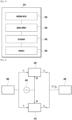
- FIG. 3 is a diagram illustrating the structure of a wireless communication module according to an embodiment of the disclosure.
- an electronic device may include at least one wireless communication module 310.
- the wireless communication module 310 may be deployed at an end of the electronic device to radiate a beam to an outside of the electronic device.
- the wireless communication module 310 may include an antenna array 320 including at least one antenna element, a phase shifter 330 configured to control a phase of a beam radiating from the antenna array 320, a processor 340 electrically connected to the phase shifter 330 and configured to perform beamforming by controlling the phase shifter 330, and a memory 350 including phase offset information of the wireless communication module 310.
- the phase offset information of the wireless communication module stored in the memory 350 may be determined based on a phase difference between the wireless communication module 310 and a reference wireless communication module.
- the reference wireless communication module may have the characteristic that is equal or similar to the characteristic of the wireless communication module 310 (even if the reference wireless communication module and the wireless communication module are manufactured to have the same characteristic, the characteristics of both the modules may be different from each other due to semiconductor process dispersion).
- FIG. 3 is a diagram illustrating the structure of the wireless communication module according to an embodiment disclosed in the disclosure. Accordingly, the structure of the wireless communication module disclosed in the disclosure should not be limited to the structure of the wireless communication module as illustrated in FIG. 3 .
- the processor 340 may also be directly and electrically connected to the antenna array 320.
- FIG. 4 is a diagram illustrating a method for determining phase offset information according to an embodiment of the disclosure.
- phase offset information of a wireless communication module may be determined based on a phase difference between a wireless communication module 410 and a reference wireless communication module 420.
- the reference wireless communication module 420 may have the characteristic that is equal or similar to the characteristic of the wireless communication module 410.
- a signal generator 430 may transmit the same signal f 1 to the wireless communication module 410 and the reference wireless communication module 420.
- the wireless communication module 410 and the reference wireless communication module 420 may receive a local oscillator (LO) signal for changing the phase of the f 1 signal received from the signal generator 430 from a local oscillator (LO) generator 450.
- LO local oscillator
- the wireless communication module 410 may output an f 3 signal based on the f 1 signal and the LO signal. For example, there may be a difference as much as ⁇ 1 between the phase of the f 3 signal and the phase of the f 1 signal.
- the reference wireless communication module 420 may output an f 2 signal based on the f 1 signal and the LO signal. For example, there may be a difference as much as ⁇ 2 between the phase of the f 2 signal and the phase of the f 1 signal.
- the phase of ⁇ 1 that is changed by the wireless communication module 410 and the phase of ⁇ 2 that is changed by the reference wireless communication module 420 may have different values due to the semiconductor process dispersion. Accordingly, in order to accurately test the performance of the wireless communication module 410, it is necessary to know the phase dispersion occurring in the wireless communication module 410 due to the semiconductor process dispersion.
- the f 3 signal output from the wireless communication module 410 and the f 2 signal output from the reference wireless communication module 420 may be added and transmitted to a spectrum analyzer 440.
- the phase dispersion of the wireless communication module 410 may be identified based on the characteristic of the (f 2 +f 3 ) signal being analyzed by the spectrum analyzer 440.
- the output signal f 2 of the wireless communication module 410 and the output signal f 3 of the reference wireless communication module 420 may act mutually as constructive interferences through adjustment of the phase shifter included in the wireless communication module 410. According to various embodiments, it may be identified through the spectrum analyzer 440 whether the f 2 signal and the f 3 signal act mutually as constructive interferences.
- ⁇ denotes phase dispersion of the wireless communication module
- ⁇ ps denotes a phase change value by the phase shifter of the wireless communication module.
- the output signal f 2 of the wireless communication module 410 and the output signal f 3 of the reference wireless communication module 420 may act mutually as destructive interferences through adjustment of the phase shifter included in the wireless communication module 410. According to various embodiments, it may be identified through the spectrum analyzer 440 whether the fz signal and the f 3 signal act mutually as destructive interferences.
- ⁇ denotes phase dispersion of the wireless communication module
- ⁇ ps denotes a phase change value by the phase shifter of the wireless communication module.
- the phase dispersion value of the wireless communication module 410 may be determined based on the Equation 1 or 2. According to various embodiments, the determined phase dispersion value may be stored in a memory of the wireless communication module or a register provided inside the processor, and the stored phase dispersion value may be used in a performance test of the wireless communication module.
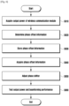
- FIG. 5 is a flowchart illustrating a method for testing a wireless communication module according to an embodiment of the disclosure.
- phase offset information stored in a memory of a wireless communication module may be acquired.
- the phase offset information may be determined based on a phase difference between the wireless communication module and a reference wireless communication module.
- the phase offset information may be a phase dispersion value of the wireless communication module.
- a phase shifter of the wireless communication module may be adjusted based on the phase offset information. For example, if the phase offset information is +10°the phase dispersion value of the wireless communication module including the phase offset information may be +10°In this case, if it is intended to form a beam in the direction of +40°through the wireless communication module, the phase shifter may be adjusted as much as +30° in consideration of the phase dispersion value of +10°
- the output power or beamforming performance of the wireless communication module may be tested.
- the beamforming performances of a plurality of wireless communication modules included in the electronic device may be tested.
- FIG. 6 is a flowchart illustrating a method for testing a wireless communication module including a method for determining phase offset information according to an embodiment of the disclosure.
- the output power of a wireless communication module and the output power of a reference wireless communication module may be acquired.
- the output power of the wireless communication module and the output power of the reference wireless communication module may be transmitted to a spectrum analyzer, and the sum of the output of the wireless communication module and the output of the reference wireless communication module may be acquired through the spectrum analyzer.
- phase offset information of the wireless communication module may be determined based on the sum of the output power of the wireless communication module and the output power of the reference wireless communication module.
- the detailed explanation of operation S620 will be described later with reference to FIGS. 7 to 10 .
- the determined phase offset information may be stored in a memory of the wireless communication module.
- the phase offset information may be stored in a register included in a wireless communication module processor.
- the phase offset information may be the phase dispersion value of the wireless communication module.
- Operations S640, S650, and S660 as illustrated in FIG. 6 may be equal or similar to the operations S510, S520, and S530 as illustrated in FIG. 5 . Accordingly, explanation of the operations S640, S650, and S660 of FIG. 6 is replaced by the explanation with reference to FIG. 5 .
- FIG. 7 is a flowchart illustrating a method for determining phase offset information according to a first embodiment of the disclosure. According to an embodiment, the flowchart as illustrated in FIG. 7 may be included in operation S620 of FIG. 6 .
- the sum of an output power of a wireless communication module and an output power of a reference wireless communication module may be identified through adjustment of a phase shifter of the wireless communication module.
- an output signal of the wireless communication module and an output signal of the reference wireless communication module may be transmitted to a spectrum analyzer, and the sum of the output power of the wireless communication module and the output power of the reference wireless communication module may be identified through the spectrum analyzer.
- operation S720 it may be identified whether the sum of the output power of the wireless communication module and the output power of the reference wireless communication module has the maximum value. According to various embodiments, if the sum of the output power of the wireless communication module and the output power of the reference wireless communication module has the maximum value, the adjustment of the phase shifter may be stopped, and at operation S730, phase offset information of the wireless communication module may be determined. According to an embodiment, if the sum of the output power of the wireless communication module and the output power of the reference wireless communication module does not have the maximum value, the operation returns to the operation S710, and the sum of the output power of the wireless communication module and the output power of the reference wireless communication module may be identified through adjustment of the phase shifter of the wireless communication module.
- the phase offset information of the wireless communication module may be determined based on the phase value of the phase shifter of the wireless communication module whereby the sum of the output power of the wireless communication module and the output power of the reference wireless communication module has the maximum value.
- the phase offset information of the wireless communication module may be determined based on Equation 3 below.
- ⁇ denotes phase offset information of the wireless communication module
- ⁇ ps denotes a phase value of the phase shifter of the wireless communication module if the sum of the output power of the wireless communication module and the output power of the reference wireless communication module has the maximum value.
- FIG. 8 is a flowchart illustrating a method for determining phase offset information according to a second embodiment of the disclosure. According to an embodiment, the flowchart as illustrated in FIG. 8 may be included in operation S620 of FIG. 6 .
- the sum of an output power of a wireless communication module and an output power of a reference wireless communication module may be identified through adjustment of a phase shifter of the wireless communication module.
- an output signal of the wireless communication module and an output signal of the reference wireless communication module may be transmitted to a spectrum analyzer, and the sum of the output power of the wireless communication module and the output power of the reference wireless communication module may be identified through the spectrum analyzer.
- operation S820 it may be identified whether the sum of the output power of the wireless communication module and the output power of the reference wireless communication module has the minimum value. According to various embodiments, if the sum of the output power of the wireless communication module and the output power of the reference wireless communication module has the minimum value, the adjustment of the phase shifter may be stopped, and at operation S830, phase offset information of the wireless communication module may be determined. According to an embodiment, if the sum of the output power of the wireless communication module and the output power of the reference wireless communication module does not have the minimum value, the operation returns to the operation S810, and the sum of the output power of the wireless communication module and the output power of the reference wireless communication module may be identified through adjustment of the phase shifter of the wireless communication module.
- the phase offset information of the wireless communication module may be determined based on the phase value of the phase shifter of the wireless communication module whereby the sum of the output power of the wireless communication module and the output power of the reference wireless communication module has the minimum value.
- ⁇ denotes phase offset information of the wireless communication module
- ⁇ ps denotes a phase value of the phase shifter of the wireless communication module if the sum of the output power of the wireless communication module and the output power of the reference wireless communication module has the minimum value.
- FIG. 9 is a flowchart illustrating a method for determining phase offset information according to a third embodiment of the disclosure. According to an embodiment, the flowchart as illustrated in FIG. 9 may be included in operation S620 of FIG. 6 .
- the correlations between a frequency output of a wireless communication module and a frequency output of a reference wireless communication module may be identified through adjustment of a phase shifter of the wireless communication module.
- an output signal of the wireless communication module and an output signal of the reference wireless communication module may be transmitted to a spectrum analyzer, and the correlations between the frequency output of the wireless communication module and the frequency output of the reference wireless communication module may be identified through the spectrum analyzer.
- phase offset information may be determined based on a phase value of the phase shifter whereby the frequency output of the wireless communication module and the frequency output of the reference wireless communication module are in mutual constructive interference relations.
- the phase offset information of the wireless communication module may be determined based on Equation 5 below.
- ⁇ denotes phase offset information of the wireless communication module
- ⁇ ps denotes a phase value of the phase shifter of the wireless communication module if the frequency output of the wireless communication module and the frequency output of the reference wireless communication module are mutual constructive interferences.
- FIG. 10 is a flowchart illustrating a method for determining phase offset information according to a fourth embodiment of the disclosure. According to an embodiment, the flowchart as illustrated in FIG. 10 may be included in operation S620 of FIG. 6 .
- the correlations between a frequency output of a wireless communication module and a frequency output of a reference wireless communication module may be identified through adjustment of a phase shifter of the wireless communication module.
- an output signal of the wireless communication module and an output signal of the reference wireless communication module may be transmitted to a spectrum analyzer, and the correlations between the frequency output of the wireless communication module and the frequency output of the reference wireless communication module may be identified through the spectrum analyzer.
- phase offset information may be determined based on a phase value of the phase shifter whereby the frequency output of the wireless communication module and the frequency output of the reference wireless communication module are in mutual destructive interference relations.
- ⁇ denotes phase offset information of the wireless communication module
- ⁇ ps denotes a phase value of the phase shifter of the wireless communication module if the frequency output of the wireless communication module and the frequency output of the reference wireless communication module are mutual constructive interferences.
- the disclosure provides an electronic device including a wireless communication module, wherein the wireless communication module includes an antenna array including at least one antenna element, a phase shifter configured to control a phase of a beam radiating from the antenna array, a processor electrically connected to the phase shifter and configured to perform beamforming by controlling the phase shifter, and a memory including phase offset information of the wireless communication module.
- the wireless communication module includes an antenna array including at least one antenna element, a phase shifter configured to control a phase of a beam radiating from the antenna array, a processor electrically connected to the phase shifter and configured to perform beamforming by controlling the phase shifter, and a memory including phase offset information of the wireless communication module.
- the phase offset information may be determined based on a phase difference between the wireless communication module and a reference wireless communication module.
- the phase offset information may be determined based on a phase value being controlled by a phase shifter included in the wireless communication module.
- the phase offset information may be determined based on a phase value being controlled by a phase shifter included in the wireless communication module.
- the phase offset information may be determined based on a phase value being controlled by a phase shifter included in the wireless communication module.
- the phase offset information may be determined based on a phase value being controlled by a phase shifter included in the wireless communication module.
- the disclosure provides a method for testing a wireless communication module which includes acquiring phase offset information stored in a memory of the wireless communication module, adjusting a phase shifter of the wireless communication module based on the phase offset information, and testing an output power and beamforming performance of the wireless communication module.
- the method may include acquiring the output power of the wireless communication module and an output power of a reference wireless communication module before acquiring the phase offset information, determining the phase offset information based on a sum of the output power of the wireless communication module and the output power of the reference wireless communication module, and storing the determined phase offset information in the memory.
- Determining the phase offset information may include identifying a sum of the output power of the wireless communication module and the output power of the reference wireless communication module by adjusting the phase shifter, and determining the phase offset information based on a phase value of the phase shifter whereby the sum of the output power of the wireless communication module and the output power of the reference wireless communication module has a maximum value.
- Determining the phase offset information may include identifying a sum of the output power of the wireless communication module and the output power of the reference wireless communication module by adjusting the phase shifter, and determining the phase offset information based on a phase value of the phase shifter whereby the sum of the output power of the wireless communication module and the output power of the reference wireless communication module has a minimum value.
- Determining the phase offset information may include identifying correlations between a frequency output of the wireless communication module and a frequency output of the reference wireless communication module by adjusting the phase shifter, and determining the phase offset information based on a phase value of the phase shifter whereby the frequency output of the wireless communication module and the frequency output of the reference wireless communication module are in mutual constructive interference relations.
- Determining the phase offset information may include identifying correlations between a frequency output of the wireless communication module and a frequency output of the reference wireless communication module by adjusting the phase shifter, and determining the phase offset information based on a phase value of the phase shifter whereby the frequency output of the wireless communication module and the frequency output of the reference wireless communication module are in mutual destructive interference relations.
- the disclosure provides a base station including a wireless communication module, wherein the wireless communication module includes an antenna array including at least one antenna element, a phase shifter configured to control a phase of a beam radiating from the antenna array, a processor electrically connected to the phase shifter and configured to perform beamforming by controlling the phase shifter, and a memory including phase offset information of the wireless communication module.
- the wireless communication module includes an antenna array including at least one antenna element, a phase shifter configured to control a phase of a beam radiating from the antenna array, a processor electrically connected to the phase shifter and configured to perform beamforming by controlling the phase shifter, and a memory including phase offset information of the wireless communication module.
- the phase offset information may be determined based on a phase difference between the wireless communication module and a reference wireless communication module.
- the phase offset information may be determined based on a phase value being controlled by a phase shifter included in the wireless communication module.
- the phase offset information may be determined based on a phase value being controlled by a phase shifter included in the wireless communication module.
- the phase offset information may be determined based on a phase value being controlled by a phase shifter included in the wireless communication module.
- the phase offset information may be determined based on a phase value being controlled by a phase shifter included in the wireless communication module.
Landscapes
- Engineering & Computer Science (AREA)
- Computer Networks & Wireless Communication (AREA)
- Signal Processing (AREA)
- Physics & Mathematics (AREA)
- Electromagnetism (AREA)
- Variable-Direction Aerials And Aerial Arrays (AREA)
- Radio Transmission System (AREA)
- Mobile Radio Communication Systems (AREA)
Description
- The disclosure provides a method and an apparatus for efficiently testing a wireless communication module in a wireless communication system in which beamforming is performed.
- To meet the increasing demand for wireless data traffic since the deployment of 4th-Generation (4G) communication systems, efforts have been made to develop an improved 5th-Generation (5G) or pre-5G communication system. Therefore, the 5G or pre-5G communication system is also called a "beyond 4G network" communication system or a "post Long Term Evolution (LTE) System." Implementation of the 5G communication system in ultrahigh frequency (mmWave) bands, e.g., 60 GHz bands, is being considered in order to accomplish higher data rates. To mitigate a path loss of the radio waves and increase the transmission distance on the radio waves in the ultrahigh frequency bands, beamforming, massive multiple-input multiple-output (massive MIMO), full dimensional MIMO (FD-MIMO), array antenna, analog beamforming, and large scale antenna techniques are being discussed for 5G communication systems. In addition, in 5G communication systems, development for system network improvement is under way based on evolved small cells, advanced small cells, cloud radio access networks (cloud RANs), ultra-dense networks, device-to-device (D2D) communication, wireless backhaul, moving network, cooperative communication, coordinated multi-points (CoMP), reception-end interference cancellation, and the like. In addition, in the 5G system, hybrid FSK and QAM modulation (FQAM) and sliding window superposition coding (SWSC), as advanced coding modulation (ACM) systems, and filter bank multi carrier (FBMC), non-orthogonal multiple access (NOMA), and sparse code multiple access (SCMA), as advanced access technologies, have been developed.
- On the other hand, the Internet, which is a human centered connectivity network where humans generate and consume information, is now evolving to the Internet of things (IoT) where distributed entities, such as things, exchange and process information without human intervention. The Internet of everything (IoE), which is a combination of IoT technology and big data processing technology through connection with a cloud server, has emerged. Technology elements, such as "sensing technology", "wired/wireless communication and network infrastructure", "service interface technology", and "security technology" have been demanded for IoT implementation; therefore, technologies, such as a sensor network, machine-to-machine (M2M) communication, machine type communication (MTC) for a connection between things, are recently researched. Such an IoT environment may provide intelligent Internet technology (IT) services that create a new value for human life by collecting and analyzing data generated among connected things. IoT may be applied to a variety of fields including smart home, smart building, smart city, smart car or connected car, smart grid, health care, smart appliances, and advanced medical services through convergence and combination between existing information technology (IT) and various industrial applications.
- In line with this, various attempts have been made to apply 5G communication systems to IoT networks. For example, technologies such as a sensor network, machine-to-machine (M2M) communication, and machine type communication (MTC) may be implemented by beamforming, MIMO, and array antennas, which correspond to 5G communication technology. Application of a cloud radio access network (cloud RAN) as the above-described big data processing technology may also be considered to be an example of convergence between the 5G technology and the IoT technology.
-
EP 2 958 255 A1 discloses a communication apparatus including: a switching device which modulates at least one of a first signal with a first frequency and passed through a first communication device and a second signal not passed through the first communication device at a second frequency lower than the first frequency; a signal combiner which combines together the first and second signals, at least one of which is modulated, to generate a composite signal containing a switching frequency component with an amplitude in response to the phase difference between the first and second signals at the second frequency; and a control unit which, based on the switching frequency component, obtains as a reference phase adjustment amount a phase adjustment amount applied by a phase adjuster in the first communication device. -
US 2017/0222849 A1 discloses a wireless device including a plurality of antennas and a plurality of wireless modules that transmit or receive signals via the plurality of antennas, wherein each of the plurality of wireless modules includes: a generator that generates a high-frequency signal; and a high-frequency circuit that transmits or receives, based on the generated high-frequency signal, a signal via at least one of the plurality of antennas. The wireless device further includes a controller that obtains, each time the plurality of wireless modules start generation of a plurality of the high-frequency signals, a difference of phases of the plurality of high-frequency signals, and controls, based on the obtained difference, at least one phase of a plurality of signals to be transmitted or received by the plurality of wireless modules. - The above information is presented as background information only to assist with an understanding of the disclosure. No determination has been made, and no assertion is made, as to whether any of the above might be applicable as prior art with regard to the disclosure.
- In the next generation mobile communication system to which beamforming is applied, the number of wireless communication modules included in the electronic device may increase.
- Accordingly, the time required to test the performance of the wireless communication module included in the electronic device may be increased.
- In the next-generation mobile communication system to which beamforming is applied, the number of wireless communication modules included in an electronic device may be increased. Accordingly, the time required to test the performances of the wireless communication modules included in the electronic device may also be increased.
- Aspects of the disclosure are to address at least the above-mentioned problems and/or disadvantages and to provide at least the advantages described below. Accordingly, an aspect of the disclosure is to provide a method and an apparatus for efficiently testing a wireless communication module in a wireless communication system in which beamforming is performed.
- Additional aspects will be set forth in part in the description which follows and, in part, will be apparent from the description, or may be learned by practice of the presented embodiments.
- In accordance with an embodiment of the disclosure, an electronic device is provided as defined in the appended claims. In accordance with another embodiment of the disclosure, a method for testing a wireless communication module is provided as defined in the appended claims. In accordance with another embodiment of the disclosure, a base station is provided as defined in the appended claims. According to the embodiments of the disclosure, the time required to test the performance of the wireless communication module can be reduced. In addition, according to the embodiments disclosed in the disclosure, the beamforming can be performed in consideration of the performances of the respective wireless communication modules.
- Other aspects, advantages, and salient features of the disclosure will become apparent to those skilled in the art from the following detailed description, which, taken in conjunction with the annexed drawings, discloses various embodiments of the disclosure.
- According to one embodiment disclosed in the present invention, the time required for wireless communication module performance test can be reduced. In addition, according to the exemplary embodiment disclosed in the present invention, beamforming in consideration of the performance of each wireless communication module may be performed.
- The above and other aspects, features and advantages of certain embodiments of the disclosure will be more apparent from the following description, taken in conjunction with the accompanying drawings, in which:
-
FIG. 1 is a diagram illustrating beam sweeping through a wireless communication module according to an embodiment of the disclosure; -
FIG. 2 is a diagram illustrating an electronic device including a plurality of wireless communication modules according to an embodiment of the disclosure; -
FIG. 3 is a diagram illustrating the structure of a wireless communication module according to an embodiment of the disclosure; -
FIG. 4 is a diagram illustrating a method for determining phase offset information according to an embodiment of the disclosure; -
FIG. 5 is a flowchart illustrating a method for testing a wireless communication module according to an embodiment of the disclosure; -
FIG. 6 is a flowchart illustrating a method for testing a wireless communication module including a method for determining phase offset information according to an embodiment of the disclosure; -
FIG. 7 is a flowchart illustrating a method for determining phase offset information according to an embodiment of the disclosure; -
FIG. 8 is a flowchart illustrating a method for determining phase offset information according to an embodiment of the disclosure; -
FIG. 9 is a flowchart illustrating a method for determining phase offset information according to an embodiment of the disclosure; and -
FIG. 10 is a flowchart illustrating a method for determining phase offset information according to an embodiment of the disclosure. - Throughout the drawings, like reference numerals will be understood to refer to like parts, components, and structures.
- The following description with reference to the accompanying drawings is provided to assist in a comprehensive understanding of various embodiments of the disclosure as defined by the claims. It includes various specific details to assist in that understanding but these are to be regarded as merely exemplary. Accordingly, those of ordinary skill in the art will recognize that various changes and modifications of the various embodiments described herein can be made without departing from the scope of the disclosure. In addition, descriptions of well-known functions and constructions may be omitted for clarity and conciseness.
- The terms and words used in the following description and claims are not limited to the bibliographical meanings, but, are merely used by the inventor to enable a clear and consistent understanding of the disclosure. Accordingly, it should be apparent to those skilled in the art that the following description of various embodiments of the disclosure is provided for illustration purpose only and not for the purpose of limiting the disclosure as defined by the appended claims.
- It is to be understood that the singular forms "a," "an," and "the" include plural referents unless the context clearly dictates otherwise. Thus, for example, reference to "a component surface" includes reference to one or more of such surfaces.
- For the same reason, in the accompanying drawings, sizes and relative sizes of some constituent elements may be exaggerated, omitted, or briefly illustrated. Further, sizes of the respective constituent elements do not completely reflect the actual sizes thereof. In the drawings, the same drawing reference numerals are used for the same or corresponding elements across various figures.
- The aspects and features of the disclosure and methods for achieving the aspects and features will be apparent by referring to the embodiments to be described in detail with reference to the accompanying drawings. However, the disclosure is not limited to the embodiments disclosed hereinafter, and it can be implemented in diverse forms. The matters defined in the description, such as the detailed construction and elements, are only specific details provided to assist those of ordinary skill in the art in a comprehensive understanding of the disclosure, and the disclosure is only defined within the scope of the appended claims. In the entire description of the disclosure, the same drawing reference numerals are used for the same elements across various figures.
- In this case, it will be understood that each block of the flowchart illustrations, and combinations of blocks in the flowchart illustrations, can be implemented by computer program instructions. These computer program instructions can be provided to a processor of a general purpose computer, special purpose computer, or other programmable data processing apparatus to produce a machine, such that the instructions, which execute via the processor of the computer or other programmable data processing apparatus, create means for implementing the functions specified in the flowchart block or blocks. These computer program instructions may also be stored in a computer usable or computer-readable memory that can direct a computer or other programmable data processing apparatus to function in a particular manner, such that the instructions stored in the computer usable or computer-readable memory produce an article of manufacture including instruction means that implement the function specified in the flowchart block or blocks. The computer program instructions may also be loaded onto a computer or other programmable data processing apparatus to cause a series of operations to be performed on the computer or other programmable apparatus to produce a computer implemented process such that the instructions that execute on the computer or other programmable apparatus provide operations for implementing the functions specified in the flowchart block or blocks.
- Also, each block of the flowchart illustrations may represent a module, segment, or portion of code, which includes one or more executable instructions for implementing the specified logical function(s). It should also be noted that in some alternative implementations, the functions noted in the blocks may occur out of the order. For example, two blocks shown in succession may in fact be executed substantially concurrently or the blocks may sometimes be executed in the reverse order, depending upon the functionality involved.
- In this case, the term "-unit", as used in an embodiment, means, but is not limited to, a software or hardware component, such as field programmable gate array (FPGA) or application specific integrated circuit (ASIC), which performs certain tasks. However, "-unit" is not meant to be limited to software or hardware. The term "-unit" may advantageously be configured to reside on the addressable storage medium and configured to execute on one or more processors. Thus, "-unit" may include, by way of example, components, such as software components, object-oriented software components, class components and task components, processes, functions, attributes, procedures, subroutines, segments of program code, drivers, firmware, microcode, circuitry, data, databases, data structures, tables, arrays, and variables. The functionality provided for in the components and "-units" may be combined into fewer components and "-units" or further separated into additional components and "-units". Further, the components and "-units" may be implemented to operate one or more central processing units (CPUs) in a device or a security multimedia card. Further, in an embodiment, "-unit" may include one or more processors.
-
FIG. 1 is a diagram illustrating beam sweeping through a wireless communication module according to an embodiment of the disclosure. - Referring to
FIG. 1 , according to an embodiment, in the next-generation mobile communication system using mm-Wave bands, a new method that is different from the wireless communication method in the related art should be considered. In particular, in the mm-Wave bands, as the frequency becomes higher, a gain loss of a beam radiating through a wireless communication module may become higher. - According to an embodiment, in the next-generation mobile communication system using the mm-Wave bands, a multi-chain structure may be used to minimize the gain loss of the beam. For example, as illustrated in
FIG. 1 , onewireless communication module 100 may have four multi-chains, and thewireless communication module 100 may perform beam sweeping by forming beams through the multi-chains. According to various embodiments, the multi-chains may mean a plurality of radio frequency (RF) chains. - According to various embodiments, in contrast with the
wireless communication module 100 as illustrated inFIG. 1 , if necessary, up to 32 chains may be implemented in one wireless communication module. However, in the next-generation mobile communication system, according to circumstances, 256 or 1024 or more chains may be necessary in one electronic device. Accordingly, in order to solve the above-described problems, a method for configuring multi-chains using a plurality of wireless communication modules may be considered. -
FIG. 2 is a diagram illustrating an electronic device including a plurality of wireless communication modules according to an embodiment of the disclosure. - Referring to
FIG. 2 , according to an embodiment, an electronic device may include fivewireless communication modules wireless communication modules - According to an embodiment, the second
wireless communication module 220, the thirdwireless communication module 230, the fourthwireless communication module 240, and the fifthwireless communication module 250 may be deployed at ends of the electronic device to radiate beams to an outside of the electronic device. For example, the secondwireless communication module 220, the thirdwireless communication module 230, the fourthwireless communication module 240, and the fifthwireless communication module 250 may be front-end chips. According to various embodiments, the secondwireless communication module 220, the thirdwireless communication module 230, the fourthwireless communication module 240, and the fifthwireless communication module 250 may include a plurality of RF chains. In the case of using the above-described embodiment, the number of RF chains of the electronic device including the firstwireless communication module 210, the secondwireless communication module 220, the thirdwireless communication module 230, the fourthwireless communication module 240, and the fifthwireless communication module 250 may be 64 (64 RF chains = 16 RF chains * 4). - According to an embodiment, the first
wireless communication module 210 may transmit a signal having an input phase ofϕ1to the secondwireless communication module 220, the thirdwireless communication module 230, the fourthwireless communication module 240, and the fifthwireless communication module 250. According to various embodiments, based on the above-described signal, the secondwireless communication module 220, the thirdwireless communication module 230, the fourthwireless communication module 240, and the fifthwireless communication module 250 may generate beams in a specific direction. - According to an embodiment, the second
wireless communication module 220 having received the signal having the phase of ϕ1 may change the phase of ϕ1 as much as Δϕ2 in order to form the beam in the specific direction. According to various embodiments, the thirdwireless communication module 230 may change the phase of ϕ1 as much as Δϕ3 in order to form the beam in the specific direction, and the fourthwireless communication module 240 may change the phase of ϕ1 as much as Δϕ4 in order to form the beam in the specific direction. The fifthwireless communication module 250 may change the phase of ϕ1 as much as Δϕ5 in order to form the beam in the specific direction. - According to an embodiment, the phase value Δϕ2 intended to be changed through the second
wireless communication module 220 may be different from the phase value being actually changed by the secondwireless communication module 220. For example, the phase value intended to be changed through the secondwireless communication module 220 may be 30°,whereas the phase value being actually changed by the secondwireless communication module 220 may be 20°. According to various embodiments, the difference between the above-described phase values may be caused by process dispersion occurring in the process of manufacturing the wireless communication module. For example, due to the difference between values of elements, such as transistors, capacitors, and inductors, included in the wireless communication module, there may be the difference between the phase value intended to be changed through the wireless communication modules and the phase value being actually changed. - According to an embodiment, the difference between the phase value intended to be changed through the wireless communication modules and the phase value being actually changed may be increased as the frequency band intended to be radiated through the wireless communication module becomes heightened. For example, in the mm-Wave frequency bands being used in the next-generation mobile communication system, the difference between the phase values may be increased in comparison with an LTE communication system. According to various embodiments, as the number of blocks cascaded in the wireless communication module or the number of functions of the wireless communication module becomes larger, the difference between the phase values may become greater.
- According to an embodiment, in all of the second
wireless communication module 220, the thirdwireless communication module 230, the fourthwireless communication module 240, and the fifthwireless communication module 250 included in the electronic device, the difference between the phase value intended to be changed through the wireless communication module and the phase value being actually changed by the wireless communication module may exist. According to various embodiments, the electronic device may perform an accurate beamforming operation by identifying the difference between the phase value intended to be changed through each wireless communication module and the phase value being actually changed by each wireless communication module. -
FIG. 3 is a diagram illustrating the structure of a wireless communication module according to an embodiment of the disclosure. - Referring to
FIG. 3 , according to an embodiment, an electronic device may include at least onewireless communication module 310. For example, thewireless communication module 310 may be deployed at an end of the electronic device to radiate a beam to an outside of the electronic device. - According to an embodiment, the
wireless communication module 310 may include anantenna array 320 including at least one antenna element, aphase shifter 330 configured to control a phase of a beam radiating from theantenna array 320, aprocessor 340 electrically connected to thephase shifter 330 and configured to perform beamforming by controlling thephase shifter 330, and amemory 350 including phase offset information of thewireless communication module 310. - According to an embodiment, the phase offset information of the wireless communication module stored in the
memory 350 may be determined based on a phase difference between thewireless communication module 310 and a reference wireless communication module. According to various embodiments, the reference wireless communication module may have the characteristic that is equal or similar to the characteristic of the wireless communication module 310 (even if the reference wireless communication module and the wireless communication module are manufactured to have the same characteristic, the characteristics of both the modules may be different from each other due to semiconductor process dispersion). - According to an embodiment, it is possible to test the performance of the wireless communication module based on the phase offset information stored in the
memory 350. According to various embodiments, by testing the performance of the wireless communication module through acquisition of the phase offset information stored in thememory 350, the time and costs required to test the wireless communication module can be reduced. - On the other hand,
FIG. 3 is a diagram illustrating the structure of the wireless communication module according to an embodiment disclosed in the disclosure. Accordingly, the structure of the wireless communication module disclosed in the disclosure should not be limited to the structure of the wireless communication module as illustrated inFIG. 3 . For example, theprocessor 340 may also be directly and electrically connected to theantenna array 320. -
FIG. 4 is a diagram illustrating a method for determining phase offset information according to an embodiment of the disclosure. - Referring to
FIG. 4 , according to an embodiment, phase offset information of a wireless communication module may be determined based on a phase difference between awireless communication module 410 and a referencewireless communication module 420. According to various embodiments, the referencewireless communication module 420 may have the characteristic that is equal or similar to the characteristic of thewireless communication module 410. - According to an embodiment, in order to identify the phase difference between the
wireless communication module 410 and the referencewireless communication module 420, asignal generator 430 may transmit the same signal f1 to thewireless communication module 410 and the referencewireless communication module 420. According to various embodiments, thewireless communication module 410 and the referencewireless communication module 420 may receive a local oscillator (LO) signal for changing the phase of the f1 signal received from thesignal generator 430 from a local oscillator (LO)generator 450. - According to an embodiment, the
wireless communication module 410 may output an f3 signal based on the f1 signal and the LO signal. For example, there may be a difference as much as ϕ1 between the phase of the f3 signal and the phase of the f1 signal. According to various embodiments, the referencewireless communication module 420 may output an f2 signal based on the f1 signal and the LO signal. For example, there may be a difference as much as ϕ2 between the phase of the f2 signal and the phase of the f1 signal. According to an embodiment, even if thewireless communication module 410 and the referencewireless communication module 420 are manufactured to have the same characteristic, the phase of ϕ1 that is changed by thewireless communication module 410 and the phase of ϕ2 that is changed by the referencewireless communication module 420 may have different values due to the semiconductor process dispersion. Accordingly, in order to accurately test the performance of thewireless communication module 410, it is necessary to know the phase dispersion occurring in thewireless communication module 410 due to the semiconductor process dispersion. - According to an embodiment, in order to acquire the phase dispersion occurring in the
wireless communication module 410, the f3 signal output from thewireless communication module 410 and the f2 signal output from the referencewireless communication module 420 may be added and transmitted to aspectrum analyzer 440. According to various embodiments, by adjusting a phase shifter included in thewireless communication module 410, the phase dispersion of thewireless communication module 410 may be identified based on the characteristic of the (f2+f3) signal being analyzed by thespectrum analyzer 440. - According to an embodiment, the output signal f2 of the
wireless communication module 410 and the output signal f3 of the referencewireless communication module 420 may act mutually as constructive interferences through adjustment of the phase shifter included in thewireless communication module 410. According to various embodiments, it may be identified through thespectrum analyzer 440 whether the f2 signal and the f3 signal act mutually as constructive interferences. - According to an embodiment, if the sum of the f2 signal and the f3 signal being identified through the
spectrum analyzer 440 has the maximum value, it can be identified that the f2 signal and the f3 signal act mutually as the constructive interferences. According to various embodiments, if the f2 signal and the f3 signal act mutually as the constructive interferences, the phase dispersion value of thewireless communication module 410 may be determined based on the phase change value by the phase shifter of thewireless communication module 410. For example, the phase dispersion of thewireless communication module 410 may be determined based on Equation 1 below.
- Here, Δϕ denotes phase dispersion of the wireless communication module, and ϕps denotes a phase change value by the phase shifter of the wireless communication module.
- According to an embodiment, the output signal f2 of the
wireless communication module 410 and the output signal f3 of the referencewireless communication module 420 may act mutually as destructive interferences through adjustment of the phase shifter included in thewireless communication module 410. According to various embodiments, it may be identified through thespectrum analyzer 440 whether the fz signal and the f3 signal act mutually as destructive interferences. - According to an embodiment, if the sum of the fz signal and the f3 signal being identified through the
spectrum analyzer 440 has the minimum value, it can be identified that the fz signal and the f3 signal act mutually as the destructive interferences. According to various embodiments, if the fz signal and the f3 signal act mutually as the destructive interferences, the phase dispersion value of thewireless communication module 410 may be determined based on the phase change value by the phase shifter of thewireless communication module 410. For example, the phase dispersion of thewireless communication module 410 may be determined based on Equation 2 below.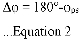
- Here, Δϕ denotes phase dispersion of the wireless communication module, and ϕps denotes a phase change value by the phase shifter of the wireless communication module.
- According to an embodiment, The phase dispersion value of the
wireless communication module 410 may be determined based on the Equation 1 or 2. According to various embodiments, the determined phase dispersion value may be stored in a memory of the wireless communication module or a register provided inside the processor, and the stored phase dispersion value may be used in a performance test of the wireless communication module. -
FIG. 5 is a flowchart illustrating a method for testing a wireless communication module according to an embodiment of the disclosure. - Referring to
FIG. 5 , according to an embodiment, at operation S510, phase offset information stored in a memory of a wireless communication module may be acquired. According to various embodiments, the phase offset information may be determined based on a phase difference between the wireless communication module and a reference wireless communication module. For example, the phase offset information may be a phase dispersion value of the wireless communication module. - According to an embodiment, at operation S520, a phase shifter of the wireless communication module may be adjusted based on the phase offset information. For example, if the phase offset information is +10°the phase dispersion value of the wireless communication module including the phase offset information may be +10°In this case, if it is intended to form a beam in the direction of +40°through the wireless communication module, the phase shifter may be adjusted as much as +30° in consideration of the phase dispersion value of +10°
- According to an embodiment, at operation S530, the output power or beamforming performance of the wireless communication module may be tested. According to various embodiments, at operation S530, the beamforming performances of a plurality of wireless communication modules included in the electronic device may be tested.
-
FIG. 6 is a flowchart illustrating a method for testing a wireless communication module including a method for determining phase offset information according to an embodiment of the disclosure. - Referring to
FIG. 6 , according to an embodiment, at operation S610, the output power of a wireless communication module and the output power of a reference wireless communication module may be acquired. According to various embodiments, the output power of the wireless communication module and the output power of the reference wireless communication module may be transmitted to a spectrum analyzer, and the sum of the output of the wireless communication module and the output of the reference wireless communication module may be acquired through the spectrum analyzer. - According to an embodiment, at operation S620, phase offset information of the wireless communication module may be determined based on the sum of the output power of the wireless communication module and the output power of the reference wireless communication module. The detailed explanation of operation S620 will be described later with reference to
FIGS. 7 to 10 . - According to an embodiment, at operation S630, the determined phase offset information may be stored in a memory of the wireless communication module. For example, the phase offset information may be stored in a register included in a wireless communication module processor. According to various embodiments, the phase offset information may be the phase dispersion value of the wireless communication module.
- Operations S640, S650, and S660 as illustrated in
FIG. 6 may be equal or similar to the operations S510, S520, and S530 as illustrated inFIG. 5 . Accordingly, explanation of the operations S640, S650, and S660 ofFIG. 6 is replaced by the explanation with reference toFIG. 5 . -
FIG. 7 is a flowchart illustrating a method for determining phase offset information according to a first embodiment of the disclosure. According to an embodiment, the flowchart as illustrated inFIG. 7 may be included in operation S620 ofFIG. 6 . - Referring to
FIG. 7 , according to an embodiment, at operation S710, the sum of an output power of a wireless communication module and an output power of a reference wireless communication module may be identified through adjustment of a phase shifter of the wireless communication module. According to various embodiments, an output signal of the wireless communication module and an output signal of the reference wireless communication module may be transmitted to a spectrum analyzer, and the sum of the output power of the wireless communication module and the output power of the reference wireless communication module may be identified through the spectrum analyzer. - According to an embodiment, at operation S720, it may be identified whether the sum of the output power of the wireless communication module and the output power of the reference wireless communication module has the maximum value. According to various embodiments, if the sum of the output power of the wireless communication module and the output power of the reference wireless communication module has the maximum value, the adjustment of the phase shifter may be stopped, and at operation S730, phase offset information of the wireless communication module may be determined. According to an embodiment, if the sum of the output power of the wireless communication module and the output power of the reference wireless communication module does not have the maximum value, the operation returns to the operation S710, and the sum of the output power of the wireless communication module and the output power of the reference wireless communication module may be identified through adjustment of the phase shifter of the wireless communication module.
- According to an embodiment, at operation S730, the phase offset information of the wireless communication module may be determined based on the phase value of the phase shifter of the wireless communication module whereby the sum of the output power of the wireless communication module and the output power of the reference wireless communication module has the maximum value. For example, the phase offset information of the wireless communication module may be determined based on Equation 3 below.

- Here, Δϕ denotes phase offset information of the wireless communication module, and ϕpsdenotes a phase value of the phase shifter of the wireless communication module if the sum of the output power of the wireless communication module and the output power of the reference wireless communication module has the maximum value.
-
FIG. 8 is a flowchart illustrating a method for determining phase offset information according to a second embodiment of the disclosure. According to an embodiment, the flowchart as illustrated inFIG. 8 may be included in operation S620 ofFIG. 6 . - Referring to
FIG. 8 , according to an embodiment, at operation S810, the sum of an output power of a wireless communication module and an output power of a reference wireless communication module may be identified through adjustment of a phase shifter of the wireless communication module. According to various embodiments, an output signal of the wireless communication module and an output signal of the reference wireless communication module may be transmitted to a spectrum analyzer, and the sum of the output power of the wireless communication module and the output power of the reference wireless communication module may be identified through the spectrum analyzer. - According to an embodiment, at operation S820, it may be identified whether the sum of the output power of the wireless communication module and the output power of the reference wireless communication module has the minimum value. According to various embodiments, if the sum of the output power of the wireless communication module and the output power of the reference wireless communication module has the minimum value, the adjustment of the phase shifter may be stopped, and at operation S830, phase offset information of the wireless communication module may be determined. According to an embodiment, if the sum of the output power of the wireless communication module and the output power of the reference wireless communication module does not have the minimum value, the operation returns to the operation S810, and the sum of the output power of the wireless communication module and the output power of the reference wireless communication module may be identified through adjustment of the phase shifter of the wireless communication module.
- According to an embodiment, at operation S830, the phase offset information of the wireless communication module may be determined based on the phase value of the phase shifter of the wireless communication module whereby the sum of the output power of the wireless communication module and the output power of the reference wireless communication module has the minimum value. For example, the phase offset information of the wireless communication module may be determined based on Equation 4 below.

- Here, Δϕ denotes phase offset information of the wireless communication module, and ϕpsdenotes a phase value of the phase shifter of the wireless communication module if the sum of the output power of the wireless communication module and the output power of the reference wireless communication module has the minimum value.
-
FIG. 9 is a flowchart illustrating a method for determining phase offset information according to a third embodiment of the disclosure. According to an embodiment, the flowchart as illustrated inFIG. 9 may be included in operation S620 ofFIG. 6 . - Referring to
FIG. 9 , according to an embodiment, at operation S910, the correlations between a frequency output of a wireless communication module and a frequency output of a reference wireless communication module may be identified through adjustment of a phase shifter of the wireless communication module. According to various embodiments, an output signal of the wireless communication module and an output signal of the reference wireless communication module may be transmitted to a spectrum analyzer, and the correlations between the frequency output of the wireless communication module and the frequency output of the reference wireless communication module may be identified through the spectrum analyzer. - According to an embodiment, at operation S920, phase offset information may be determined based on a phase value of the phase shifter whereby the frequency output of the wireless communication module and the frequency output of the reference wireless communication module are in mutual constructive interference relations. For example, the phase offset information of the wireless communication module may be determined based on Equation 5 below.

- Here, Δϕ denotes phase offset information of the wireless communication module, and ϕpsdenotes a phase value of the phase shifter of the wireless communication module if the frequency output of the wireless communication module and the frequency output of the reference wireless communication module are mutual constructive interferences.
-
FIG. 10 is a flowchart illustrating a method for determining phase offset information according to a fourth embodiment of the disclosure. According to an embodiment, the flowchart as illustrated inFIG. 10 may be included in operation S620 ofFIG. 6 . - Referring to
FIG. 10 , according to an embodiment, at operation S1010, the correlations between a frequency output of a wireless communication module and a frequency output of a reference wireless communication module may be identified through adjustment of a phase shifter of the wireless communication module. According to various embodiments, an output signal of the wireless communication module and an output signal of the reference wireless communication module may be transmitted to a spectrum analyzer, and the correlations between the frequency output of the wireless communication module and the frequency output of the reference wireless communication module may be identified through the spectrum analyzer. - According to an embodiment, at operation S1020, phase offset information may be determined based on a phase value of the phase shifter whereby the frequency output of the wireless communication module and the frequency output of the reference wireless communication module are in mutual destructive interference relations. For example, the phase offset information of the wireless communication module may be determined based on Equation 6 below.

- Here, Δϕ denotes phase offset information of the wireless communication module, and Δϕps denotes a phase value of the phase shifter of the wireless communication module if the frequency output of the wireless communication module and the frequency output of the reference wireless communication module are mutual constructive interferences.
- The disclosure provides an electronic device including a wireless communication module, wherein the wireless communication module includes an antenna array including at least one antenna element, a phase shifter configured to control a phase of a beam radiating from the antenna array, a processor electrically connected to the phase shifter and configured to perform beamforming by controlling the phase shifter, and a memory including phase offset information of the wireless communication module.
- The phase offset information may be determined based on a phase difference between the wireless communication module and a reference wireless communication module.
- If the beam radiating through the wireless communication module and a beam radiating through a reference wireless communication module act mutually as constructive interferences, the phase offset information may be determined based on a phase value being controlled by a phase shifter included in the wireless communication module.
- If the beam radiating through the wireless communication module and a beam radiating through a reference wireless communication module act mutually as destructive interferences, the phase offset information may be determined based on a phase value being controlled by a phase shifter included in the wireless communication module.
- If a sum of a power of the beam radiating through the wireless communication module and a power of a beam radiating through a reference wireless communication module has a maximum value, the phase offset information may be determined based on a phase value being controlled by a phase shifter included in the wireless communication module.
- If a sum of a power of the beam radiating through the wireless communication module and a power of a beam radiating through a reference wireless communication module has a minimum value, the phase offset information may be determined based on a phase value being controlled by a phase shifter included in the wireless communication module.
- The disclosure provides a method for testing a wireless communication module which includes acquiring phase offset information stored in a memory of the wireless communication module, adjusting a phase shifter of the wireless communication module based on the phase offset information, and testing an output power and beamforming performance of the wireless communication module.
- The method may include acquiring the output power of the wireless communication module and an output power of a reference wireless communication module before acquiring the phase offset information, determining the phase offset information based on a sum of the output power of the wireless communication module and the output power of the reference wireless communication module, and storing the determined phase offset information in the memory.
- Determining the phase offset information may include identifying a sum of the output power of the wireless communication module and the output power of the reference wireless communication module by adjusting the phase shifter, and determining the phase offset information based on a phase value of the phase shifter whereby the sum of the output power of the wireless communication module and the output power of the reference wireless communication module has a maximum value.
- Determining the phase offset information may include identifying a sum of the output power of the wireless communication module and the output power of the reference wireless communication module by adjusting the phase shifter, and determining the phase offset information based on a phase value of the phase shifter whereby the sum of the output power of the wireless communication module and the output power of the reference wireless communication module has a minimum value.
- Determining the phase offset information may include identifying correlations between a frequency output of the wireless communication module and a frequency output of the reference wireless communication module by adjusting the phase shifter, and determining the phase offset information based on a phase value of the phase shifter whereby the frequency output of the wireless communication module and the frequency output of the reference wireless communication module are in mutual constructive interference relations.
- Determining the phase offset information may include identifying correlations between a frequency output of the wireless communication module and a frequency output of the reference wireless communication module by adjusting the phase shifter, and determining the phase offset information based on a phase value of the phase shifter whereby the frequency output of the wireless communication module and the frequency output of the reference wireless communication module are in mutual destructive interference relations.
- The disclosure provides a base station including a wireless communication module, wherein the wireless communication module includes an antenna array including at least one antenna element, a phase shifter configured to control a phase of a beam radiating from the antenna array, a processor electrically connected to the phase shifter and configured to perform beamforming by controlling the phase shifter, and a memory including phase offset information of the wireless communication module.
- The phase offset information may be determined based on a phase difference between the wireless communication module and a reference wireless communication module.
- If the beam radiating through the wireless communication module and a beam radiating through a reference wireless communication module act mutually as constructive interferences, the phase offset information may be determined based on a phase value being controlled by a phase shifter included in the wireless communication module.
- If the beam radiating through the wireless communication module and a beam radiating through a reference wireless communication module act mutually as destructive interferences, the phase offset information may be determined based on a phase value being controlled by a phase shifter included in the wireless communication module.
- If a sum of a power of the beam radiating through the wireless communication module and a power of a beam radiating through a reference wireless communication module has a maximum value, the phase offset information may be determined based on a phase value being controlled by a phase shifter included in the wireless communication module.
- If a sum of a power of the beam radiating through the wireless communication module and a power of a beam radiating through a reference wireless communication module has a minimum value, the phase offset information may be determined based on a phase value being controlled by a phase shifter included in the wireless communication module.
- While the disclosure has been shown and described with reference to various embodiments thereof, it will be understood by those skilled in the art that various changes in form and details may be made therein without departing from the scope of the disclosure as defined by the appended claims.
Claims (15)
- An electronic device comprising:one or more wireless communication modules (100, 310, 410),wherein a wireless communication module (100, 310, 410) among the one or more wireless communication modules (100, 310, 410) comprises:an antenna array (320) including at least one antenna element;a phase shifter (330) configured to control a phase of a beam radiating from the antenna array (320);a processor (340) connected to the phase shifter (330) and configured to perform beamforming by controlling the phase shifter (330); anda memory (350),wherein tests for an output power and beamforming performance of the wireless communication module (100, 310, 410) are performed after adjusting the phase shifter (330) of the wireless communication module (100, 310, 410),wherein the phase shifter (330) of the wireless communication module (100, 310, 410) is adjusted based on phase offset information stored in the memory (350) of the wireless communication module (100, 310, 410),wherein the phase offset information is determined based on a phase difference between the wireless communication module (100, 310, 410) and a reference wireless communication module (420), andwherein the phase difference is based on a relationship between a frequency output of the wireless communication module (100, 310, 410) and a frequency output of the reference wireless communication module (420) or a relationship between an output power of the wireless communication module (100, 310, 410) and an output power of the reference wireless communication module (420).
- The electronic device of claim 1, wherein the phase offset information is determined based on the phase difference being controlled by the phase shifter (330) of the wireless communication module (100, 310, 410) such that the frequency output of the wireless communication module (100, 310, 410) and the frequency output of the reference wireless communication module (420) are in mutual constructive interference relations.
- The electronic device of claim 1, wherein the phase offset information is determined based on the phase difference being controlled by the phase shifter (330) of the wireless communication module (100, 310, 410) such that the frequency output of the wireless communication module (100, 310, 410) and the frequency output of the reference wireless communication module (420) are in mutual destructive interference relations.
- The electronic device of claim 1, wherein the phase offset information is determined based on the phase difference being controlled by the phase shifter (330) of the wireless communication module (100, 310, 410) such that a sum of the output power of the wireless communication module (100, 310, 410) and the output power of the reference wireless communication module (420) has a maximum value.
- The electronic device of claim 1, wherein the phase offset information is determined based on the phase difference being controlled by the phase shifter (330) of the wireless communication module (100, 310, 410) such that a sum of the output power of the wireless communication module (100, 310, 410) and the output power of the reference wireless communication module (420) has a minimum value.
- A method for testing a wireless communication module (100, 310, 410), the method comprising:determining (S510) phase offset information based on a phase difference between the wireless communication module (100, 310, 410) and a reference wireless communication module (420);storing (S510) the phase offset information in a memory (350) of the wireless communication module (100, 310, 410);adjusting (S520) a phase shifter (330) of the wireless communication module (100, 310, 410) based on the phase offset information; andperforming (S530) tests for an output power and beamforming performance of the wireless communication module (100, 310, 410) based on the adjustment of the phase shifter (330),wherein the phase difference is based on a relationship between a frequency output of the wireless communication module (100, 310, 410) and a frequency output of the reference wireless communication module (420) or a relationship between an output power of the wireless communication module (100, 310, 410) and an output power of the reference wireless communication module (420).
- The method of claim 6, wherein the determining of the phase offset information comprises:obtaining the output power of the wireless communication module (100, 310, 410) and the output power of the reference wireless communication module (420); anddetermining the phase offset information based on a sum of the output power of the wireless communication module (100, 310, 410) and the output power of the reference wireless communication module (420).
- The method of claim 7, wherein the determining of the phase offset information comprises:
determining the phase offset information based on the phase difference being controlled by the phase shifter (330) of the wireless communication module (100, 310, 410) such that the sum of the output power of the wireless communication module (100, 310, 410) and the output power of the reference wireless communication module (420) has a maximum value or a minimum value. - The method of claim 6, wherein the determining of the phase offset information comprises:
determining the phase offset information based on the phase difference being controlled by the phase shifter (330) of the wireless communication module (100, 310, 410) such that the frequency output of the wireless communication module (100, 310, 410) and the frequency output of the reference wireless communication module (420) are in mutual constructive interference relations. - The method of claim 6, wherein the determining of the phase offset information comprises:
determining the phase offset information based on the phase difference being controlled by the phase shifter (330) of the wireless communication module (100, 310, 410) such that the frequency output of the wireless communication module (100, 310, 410) and the frequency output of the reference wireless communication module (420) are in mutual destructive interference relations. - A base station comprising:one or more wireless communication modules (100, 310, 410),wherein a wireless communication module (100, 310, 410) among the one or more wireless communication modules (100, 310, 410) comprises:an antenna array (320) including at least one antenna element;a phase shifter (330) configured to control a phase of a beam radiating from the antenna array (320);a processor (340) connected to the phase shifter (330) and configured to perform beamforming by controlling the phase shifter (330); anda memory (350),wherein tests for an output power and beamforming performance of the wireless communication module (100, 310, 410) are performed after adjusting the phase shifter (330) of the wireless communication module (100, 310, 410),wherein the phase shifter (330) of the wireless communication module (100, 310, 410) is adjusted based on phase offset information stored in the memory (350) of the wireless communication module (100, 310, 410),wherein the phase offset information is determined based on a phase difference between the wireless communication module (100, 310, 410) and a reference wireless communication module (420), andwherein the phase difference is based on a relationship between a frequency output of the wireless communication module (100, 310, 410) and a frequency output of the reference wireless communication module (420) or a relationship between an output power of the wireless communication module (100, 310, 410) and an output power of the reference wireless communication module (420).
- The base station of claim 11, wherein the phase offset information is determined based on the phase difference being controlled by the phase shifter (330) of the wireless communication module (100, 310, 410) such that the frequency output of the wireless communication module (100, 310, 410) and the frequency output of the reference wireless communication module (420) are in mutual constructive interference relations.
- The base station of claim 11, wherein the phase offset information is determined based on the phase difference being controlled by the phase shifter (330) of the wireless communication module (100, 310, 410) such that the frequency output of the wireless communication module (100, 310, 410) and the frequency output of the reference wireless communication module (420) are in mutual destructive interference relations.
- The base station of claim 11, wherein the phase offset information is determined based on the phase difference being controlled by the phase shifter (330) of the wireless communication module (100, 310, 410) such that a sum of the output power of the wireless communication module (100, 310, 410) and the output power of the reference wireless communication module (420) has a maximum value.
- The base station of claim 11, wherein the phase offset information is determined based on the phase difference being controlled by the phase shifter (330) of the wireless communication module (100, 310, 410) such that a sum of the output power of the wireless communication module (100, 310, 410) and the output power of the reference wireless communication module (420) has a minimum value.
Applications Claiming Priority (2)
| Application Number | Priority Date | Filing Date | Title |
|---|---|---|---|
| KR1020180169880A KR102388027B1 (en) | 2018-12-26 | 2018-12-26 | A method for testing a wireless communication module, and an electronic device including the wireless communication module |
| PCT/KR2019/018443 WO2020138940A1 (en) | 2018-12-26 | 2019-12-26 | Method for testing wireless communication module and electronic device including the wireless communication module |
Publications (3)
| Publication Number | Publication Date |
|---|---|
| EP3827529A1 EP3827529A1 (en) | 2021-06-02 |
| EP3827529A4 EP3827529A4 (en) | 2022-01-19 |
| EP3827529B1 true EP3827529B1 (en) | 2024-02-28 |
Family
ID=71123380
Family Applications (1)
| Application Number | Title | Priority Date | Filing Date |
|---|---|---|---|
| EP19904586.5A Active EP3827529B1 (en) | 2018-12-26 | 2019-12-26 | Method for testing wireless communication module and electronic device including the wireless communication module |
Country Status (5)
| Country | Link |
|---|---|
| US (1) | US11283532B2 (en) |
| EP (1) | EP3827529B1 (en) |
| KR (1) | KR102388027B1 (en) |
| CN (1) | CN113243090B (en) |
| WO (1) | WO2020138940A1 (en) |
Families Citing this family (3)
| Publication number | Priority date | Publication date | Assignee | Title |
|---|---|---|---|---|
| CN110233315B (en) * | 2019-06-14 | 2021-12-28 | 京东方科技集团股份有限公司 | Phase shift compensation device, phase shift compensation system and method |
| CN112072301A (en) * | 2020-08-10 | 2020-12-11 | 超讯通信股份有限公司 | Dual-polarized low-profile broadband 5G base station antenna |
| TW202518871A (en) * | 2023-10-27 | 2025-05-01 | 財團法人工業技術研究院 | Beamforming chip and method for calibrating radio frequency signal |
Family Cites Families (19)
| Publication number | Priority date | Publication date | Assignee | Title |
|---|---|---|---|---|
| US5682165A (en) * | 1996-05-02 | 1997-10-28 | Hughes Electronics | Active array self calibration |
| SE509434C2 (en) * | 1997-05-16 | 1999-01-25 | Ericsson Telefon Ab L M | Antenna calibration device and method |
| WO2003043127A2 (en) * | 2001-11-14 | 2003-05-22 | Qinetiq Limited | Antenna system |
| JP2006304205A (en) | 2005-04-25 | 2006-11-02 | Nippon Hoso Kyokai <Nhk> | Antenna phase calibration apparatus and tracking antenna apparatus using the same |
| DE102006024210A1 (en) * | 2006-05-23 | 2007-11-29 | Deutsches Elektronen-Synchrotron Desy | Self-tuning drift-free radio-frequency phase detector circuit |
| WO2008146520A1 (en) * | 2007-06-01 | 2008-12-04 | Omron Corporation | Tag communication device and tag communication method |
| WO2011145264A1 (en) | 2010-05-21 | 2011-11-24 | 日本電気株式会社 | Antenna device, antenna system, and adjustment method |
| US8754811B1 (en) * | 2011-04-08 | 2014-06-17 | Lockheed Martin Corporation | Digital beamforming phased array |
| KR101801589B1 (en) | 2013-11-08 | 2017-11-27 | 엘지전자 주식회사 | Pre-compensation of the phase shifting error |
| JP6264204B2 (en) | 2014-06-17 | 2018-01-24 | 富士通株式会社 | Communication apparatus and phase adjustment method |
| KR101589429B1 (en) * | 2014-07-28 | 2016-01-28 | 정시은 | Mobile terminal and method of setting-releasing use restriction thereof |
| KR102459683B1 (en) | 2015-07-09 | 2022-10-28 | 삼성전자주식회사 | Apparatus and method for calibrating in a radio frequence module |
| WO2017014600A1 (en) * | 2015-07-22 | 2017-01-26 | 삼성전자 주식회사 | Method and device for operating machine type device in wireless communication system |
| ES2757308T3 (en) * | 2015-12-08 | 2020-04-28 | Huawei Tech Co Ltd | Method for sending data, base station and terminal device |
| JP6672846B2 (en) * | 2016-02-03 | 2020-03-25 | 富士通株式会社 | Wireless device and phase control method |
| CN107959533B (en) * | 2016-10-17 | 2020-11-06 | 华为技术有限公司 | Wireless device and radio frequency channel calibration method |
| US10620297B2 (en) * | 2016-12-22 | 2020-04-14 | Apple Inc. | Radar methods and apparatus using in phased array communication systems |
| CN107765104B (en) | 2017-09-04 | 2020-02-14 | 华为技术有限公司 | Phased array calibration method and calibration device |
| EP3729130A4 (en) * | 2017-12-19 | 2021-09-15 | The Board Of Trustees Of The Leland Stanford Junior University | METHOD AND DEVICE FOR REALIZING SCALABLE ANTENNA ARRANGEMENTS WITH LARGE APERTURE |
-
2018
- 2018-12-26 KR KR1020180169880A patent/KR102388027B1/en active Active
-
2019
- 2019-12-23 US US16/725,323 patent/US11283532B2/en active Active
- 2019-12-26 EP EP19904586.5A patent/EP3827529B1/en active Active
- 2019-12-26 CN CN201980083436.2A patent/CN113243090B/en active Active
- 2019-12-26 WO PCT/KR2019/018443 patent/WO2020138940A1/en not_active Ceased
Also Published As
| Publication number | Publication date |
|---|---|
| CN113243090A (en) | 2021-08-10 |
| US20200213017A1 (en) | 2020-07-02 |
| WO2020138940A1 (en) | 2020-07-02 |
| CN113243090B (en) | 2024-02-23 |
| KR20200080034A (en) | 2020-07-06 |
| EP3827529A1 (en) | 2021-06-02 |
| US11283532B2 (en) | 2022-03-22 |
| EP3827529A4 (en) | 2022-01-19 |
| KR102388027B1 (en) | 2022-04-19 |
Similar Documents
| Publication | Publication Date | Title |
|---|---|---|
| US10587435B2 (en) | Technique for radio channel estimation | |
| EP3985911B1 (en) | Apparatus and method for transmitting uplink signals in wireless communication system | |
| JP7514875B2 (en) | Information transmission method, device, and storage medium | |
| US11201719B2 (en) | Interference reduction in dynamic TDD systems | |
| US11101859B2 (en) | Signal transmission method and device using beamforming in wireless communication system | |
| DE112017007368T5 (en) | COOPERATIVE V2X COMMUNICATION | |
| US20230239112A1 (en) | Method and device for providing remote interference management reference signal, and storage medium | |
| US11283532B2 (en) | Method for testing wireless communication module and electronic device including the wireless communication module | |
| CN114503747B (en) | Method and apparatus for frequency layer configuration of NR positioning reference signals | |
| EP4270653A2 (en) | Beamforming antenna module comprising lens | |
| US11211979B2 (en) | Method and apparatus for controlling transmission power in wireless communication system | |
| US12388516B2 (en) | Orbital angular momentum multiplexing based on a common factor between quantities of transmit and receive antenna subarrays | |
| EP3935796B1 (en) | A method and an apparatus for determining a local frequency in wireless communication system | |
| US20240340924A1 (en) | Sidelink resource pool configuration for fr2 beam management | |
| US11528081B2 (en) | Base station and control method therefor in wireless communication system | |
| EP3675381A2 (en) | Electronic device including plurality of antenna arrays | |
| US11102792B2 (en) | Method and apparatus for demodulating signal by using subframe combination in wireless communication system | |
| US20220069924A1 (en) | Device for testing antenna module comprising plurality of antenna elements | |
| US20240322869A1 (en) | Methods for communicating training data to a machine learning server for blockage modeling and blockage mitigation | |
| WO2025208589A1 (en) | Ambient internet of things device feedback information communication | |
| WO2025076715A1 (en) | Transmit diversity for backscatter communications | |
| WO2025160789A1 (en) | Synchronization and cell searching for ambient internet-of-things devices | |
| WO2025208590A1 (en) | Ambient internet of things device control information communication | |
| WO2025123315A1 (en) | Selection of a random access channel resource using spatial beam prediction | |
| US11362419B2 (en) | Device for testing beam forming processor |
Legal Events
| Date | Code | Title | Description |
|---|---|---|---|
| STAA | Information on the status of an ep patent application or granted ep patent |
Free format text: STATUS: THE INTERNATIONAL PUBLICATION HAS BEEN MADE |
|
| PUAI | Public reference made under article 153(3) epc to a published international application that has entered the european phase |
Free format text: ORIGINAL CODE: 0009012 |
|
| STAA | Information on the status of an ep patent application or granted ep patent |
Free format text: STATUS: REQUEST FOR EXAMINATION WAS MADE |
|
| 17P | Request for examination filed |
Effective date: 20210225 |
|
| AK | Designated contracting states |
Kind code of ref document: A1 Designated state(s): AL AT BE BG CH CY CZ DE DK EE ES FI FR GB GR HR HU IE IS IT LI LT LU LV MC MK MT NL NO PL PT RO RS SE SI SK SM TR |
|
| RIC1 | Information provided on ipc code assigned before grant |
Ipc: H01Q 1/24 20060101ALN20210809BHEP Ipc: H04B 7/0456 20170101ALI20210809BHEP Ipc: H01Q 3/26 20060101ALI20210809BHEP Ipc: H04B 7/06 20060101AFI20210809BHEP |
|
| A4 | Supplementary search report drawn up and despatched |
Effective date: 20211221 |
|
| RIC1 | Information provided on ipc code assigned before grant |
Ipc: H01Q 1/24 20060101ALN20211215BHEP Ipc: H04B 7/0456 20170101ALI20211215BHEP Ipc: H01Q 3/26 20060101ALI20211215BHEP Ipc: H04B 7/06 20060101AFI20211215BHEP |
|
| DAV | Request for validation of the european patent (deleted) | ||
| DAX | Request for extension of the european patent (deleted) | ||
| REG | Reference to a national code |
Ref country code: DE Ref legal event code: R079 Free format text: PREVIOUS MAIN CLASS: H04B0017150000 Ipc: H04B0007060000 Ref document number: 602019047548 Country of ref document: DE |
|
| GRAP | Despatch of communication of intention to grant a patent |
Free format text: ORIGINAL CODE: EPIDOSNIGR1 |
|
| STAA | Information on the status of an ep patent application or granted ep patent |
Free format text: STATUS: GRANT OF PATENT IS INTENDED |
|
| RIC1 | Information provided on ipc code assigned before grant |
Ipc: H01Q 1/24 20060101ALN20231002BHEP Ipc: H04B 7/0456 20170101ALI20231002BHEP Ipc: H01Q 3/26 20060101ALI20231002BHEP Ipc: H04B 7/06 20060101AFI20231002BHEP |
|
| INTG | Intention to grant announced |
Effective date: 20231019 |
|
| GRAS | Grant fee paid |
Free format text: ORIGINAL CODE: EPIDOSNIGR3 |
|
| GRAA | (expected) grant |
Free format text: ORIGINAL CODE: 0009210 |
|
| STAA | Information on the status of an ep patent application or granted ep patent |
Free format text: STATUS: THE PATENT HAS BEEN GRANTED |
|
| AK | Designated contracting states |
Kind code of ref document: B1 Designated state(s): AL AT BE BG CH CY CZ DE DK EE ES FI FR GB GR HR HU IE IS IT LI LT LU LV MC MK MT NL NO PL PT RO RS SE SI SK SM TR |
|
| REG | Reference to a national code |
Ref country code: GB Ref legal event code: FG4D |
|
| REG | Reference to a national code |
Ref country code: CH Ref legal event code: EP |
|
| REG | Reference to a national code |
Ref country code: IE Ref legal event code: FG4D |
|
| REG | Reference to a national code |
Ref country code: DE Ref legal event code: R096 Ref document number: 602019047548 Country of ref document: DE |
|
| REG | Reference to a national code |
Ref country code: LT Ref legal event code: MG9D |
|
| PG25 | Lapsed in a contracting state [announced via postgrant information from national office to epo] |
Ref country code: IS Free format text: LAPSE BECAUSE OF FAILURE TO SUBMIT A TRANSLATION OF THE DESCRIPTION OR TO PAY THE FEE WITHIN THE PRESCRIBED TIME-LIMIT Effective date: 20240628 |
|
| REG | Reference to a national code |
Ref country code: NL Ref legal event code: MP Effective date: 20240228 |
|
| PG25 | Lapsed in a contracting state [announced via postgrant information from national office to epo] |
Ref country code: LT Free format text: LAPSE BECAUSE OF FAILURE TO SUBMIT A TRANSLATION OF THE DESCRIPTION OR TO PAY THE FEE WITHIN THE PRESCRIBED TIME-LIMIT Effective date: 20240228 |
|
| PG25 | Lapsed in a contracting state [announced via postgrant information from national office to epo] |
Ref country code: GR Free format text: LAPSE BECAUSE OF FAILURE TO SUBMIT A TRANSLATION OF THE DESCRIPTION OR TO PAY THE FEE WITHIN THE PRESCRIBED TIME-LIMIT Effective date: 20240529 |
|
| PG25 | Lapsed in a contracting state [announced via postgrant information from national office to epo] |
Ref country code: RS Free format text: LAPSE BECAUSE OF FAILURE TO SUBMIT A TRANSLATION OF THE DESCRIPTION OR TO PAY THE FEE WITHIN THE PRESCRIBED TIME-LIMIT Effective date: 20240528 Ref country code: HR Free format text: LAPSE BECAUSE OF FAILURE TO SUBMIT A TRANSLATION OF THE DESCRIPTION OR TO PAY THE FEE WITHIN THE PRESCRIBED TIME-LIMIT Effective date: 20240228 Ref country code: NL Free format text: LAPSE BECAUSE OF FAILURE TO SUBMIT A TRANSLATION OF THE DESCRIPTION OR TO PAY THE FEE WITHIN THE PRESCRIBED TIME-LIMIT Effective date: 20240228 |
|
| PG25 | Lapsed in a contracting state [announced via postgrant information from national office to epo] |
Ref country code: ES Free format text: LAPSE BECAUSE OF FAILURE TO SUBMIT A TRANSLATION OF THE DESCRIPTION OR TO PAY THE FEE WITHIN THE PRESCRIBED TIME-LIMIT Effective date: 20240228 |
|
| PG25 | Lapsed in a contracting state [announced via postgrant information from national office to epo] |
Ref country code: RS Free format text: LAPSE BECAUSE OF FAILURE TO SUBMIT A TRANSLATION OF THE DESCRIPTION OR TO PAY THE FEE WITHIN THE PRESCRIBED TIME-LIMIT Effective date: 20240528 Ref country code: NO Free format text: LAPSE BECAUSE OF FAILURE TO SUBMIT A TRANSLATION OF THE DESCRIPTION OR TO PAY THE FEE WITHIN THE PRESCRIBED TIME-LIMIT Effective date: 20240528 Ref country code: NL Free format text: LAPSE BECAUSE OF FAILURE TO SUBMIT A TRANSLATION OF THE DESCRIPTION OR TO PAY THE FEE WITHIN THE PRESCRIBED TIME-LIMIT Effective date: 20240228 Ref country code: LT Free format text: LAPSE BECAUSE OF FAILURE TO SUBMIT A TRANSLATION OF THE DESCRIPTION OR TO PAY THE FEE WITHIN THE PRESCRIBED TIME-LIMIT Effective date: 20240228 Ref country code: IS Free format text: LAPSE BECAUSE OF FAILURE TO SUBMIT A TRANSLATION OF THE DESCRIPTION OR TO PAY THE FEE WITHIN THE PRESCRIBED TIME-LIMIT Effective date: 20240628 Ref country code: HR Free format text: LAPSE BECAUSE OF FAILURE TO SUBMIT A TRANSLATION OF THE DESCRIPTION OR TO PAY THE FEE WITHIN THE PRESCRIBED TIME-LIMIT Effective date: 20240228 Ref country code: GR Free format text: LAPSE BECAUSE OF FAILURE TO SUBMIT A TRANSLATION OF THE DESCRIPTION OR TO PAY THE FEE WITHIN THE PRESCRIBED TIME-LIMIT Effective date: 20240529 Ref country code: FI Free format text: LAPSE BECAUSE OF FAILURE TO SUBMIT A TRANSLATION OF THE DESCRIPTION OR TO PAY THE FEE WITHIN THE PRESCRIBED TIME-LIMIT Effective date: 20240228 Ref country code: ES Free format text: LAPSE BECAUSE OF FAILURE TO SUBMIT A TRANSLATION OF THE DESCRIPTION OR TO PAY THE FEE WITHIN THE PRESCRIBED TIME-LIMIT Effective date: 20240228 Ref country code: BG Free format text: LAPSE BECAUSE OF FAILURE TO SUBMIT A TRANSLATION OF THE DESCRIPTION OR TO PAY THE FEE WITHIN THE PRESCRIBED TIME-LIMIT Effective date: 20240228 |
|
| PG25 | Lapsed in a contracting state [announced via postgrant information from national office to epo] |
Ref country code: PL Free format text: LAPSE BECAUSE OF FAILURE TO SUBMIT A TRANSLATION OF THE DESCRIPTION OR TO PAY THE FEE WITHIN THE PRESCRIBED TIME-LIMIT Effective date: 20240228 Ref country code: PT Free format text: LAPSE BECAUSE OF FAILURE TO SUBMIT A TRANSLATION OF THE DESCRIPTION OR TO PAY THE FEE WITHIN THE PRESCRIBED TIME-LIMIT Effective date: 20240628 |
|
| REG | Reference to a national code |
Ref country code: AT Ref legal event code: MK05 Ref document number: 1662208 Country of ref document: AT Kind code of ref document: T Effective date: 20240228 |
|
| PG25 | Lapsed in a contracting state [announced via postgrant information from national office to epo] |
Ref country code: SE Free format text: LAPSE BECAUSE OF FAILURE TO SUBMIT A TRANSLATION OF THE DESCRIPTION OR TO PAY THE FEE WITHIN THE PRESCRIBED TIME-LIMIT Effective date: 20240228 Ref country code: PT Free format text: LAPSE BECAUSE OF FAILURE TO SUBMIT A TRANSLATION OF THE DESCRIPTION OR TO PAY THE FEE WITHIN THE PRESCRIBED TIME-LIMIT Effective date: 20240628 Ref country code: PL Free format text: LAPSE BECAUSE OF FAILURE TO SUBMIT A TRANSLATION OF THE DESCRIPTION OR TO PAY THE FEE WITHIN THE PRESCRIBED TIME-LIMIT Effective date: 20240228 Ref country code: LV Free format text: LAPSE BECAUSE OF FAILURE TO SUBMIT A TRANSLATION OF THE DESCRIPTION OR TO PAY THE FEE WITHIN THE PRESCRIBED TIME-LIMIT Effective date: 20240228 |
|
| PG25 | Lapsed in a contracting state [announced via postgrant information from national office to epo] |
Ref country code: DK Free format text: LAPSE BECAUSE OF FAILURE TO SUBMIT A TRANSLATION OF THE DESCRIPTION OR TO PAY THE FEE WITHIN THE PRESCRIBED TIME-LIMIT Effective date: 20240228 |
|
| PG25 | Lapsed in a contracting state [announced via postgrant information from national office to epo] |
Ref country code: SM Free format text: LAPSE BECAUSE OF FAILURE TO SUBMIT A TRANSLATION OF THE DESCRIPTION OR TO PAY THE FEE WITHIN THE PRESCRIBED TIME-LIMIT Effective date: 20240228 |
|
| PG25 | Lapsed in a contracting state [announced via postgrant information from national office to epo] |
Ref country code: CZ Free format text: LAPSE BECAUSE OF FAILURE TO SUBMIT A TRANSLATION OF THE DESCRIPTION OR TO PAY THE FEE WITHIN THE PRESCRIBED TIME-LIMIT Effective date: 20240228 Ref country code: EE Free format text: LAPSE BECAUSE OF FAILURE TO SUBMIT A TRANSLATION OF THE DESCRIPTION OR TO PAY THE FEE WITHIN THE PRESCRIBED TIME-LIMIT Effective date: 20240228 |
|
| PG25 | Lapsed in a contracting state [announced via postgrant information from national office to epo] |
Ref country code: AT Free format text: LAPSE BECAUSE OF FAILURE TO SUBMIT A TRANSLATION OF THE DESCRIPTION OR TO PAY THE FEE WITHIN THE PRESCRIBED TIME-LIMIT Effective date: 20240228 |
|
| PG25 | Lapsed in a contracting state [announced via postgrant information from national office to epo] |
Ref country code: SK Free format text: LAPSE BECAUSE OF FAILURE TO SUBMIT A TRANSLATION OF THE DESCRIPTION OR TO PAY THE FEE WITHIN THE PRESCRIBED TIME-LIMIT Effective date: 20240228 |
|
| PG25 | Lapsed in a contracting state [announced via postgrant information from national office to epo] |
Ref country code: SM Free format text: LAPSE BECAUSE OF FAILURE TO SUBMIT A TRANSLATION OF THE DESCRIPTION OR TO PAY THE FEE WITHIN THE PRESCRIBED TIME-LIMIT Effective date: 20240228 Ref country code: SK Free format text: LAPSE BECAUSE OF FAILURE TO SUBMIT A TRANSLATION OF THE DESCRIPTION OR TO PAY THE FEE WITHIN THE PRESCRIBED TIME-LIMIT Effective date: 20240228 Ref country code: RO Free format text: LAPSE BECAUSE OF FAILURE TO SUBMIT A TRANSLATION OF THE DESCRIPTION OR TO PAY THE FEE WITHIN THE PRESCRIBED TIME-LIMIT Effective date: 20240228 Ref country code: EE Free format text: LAPSE BECAUSE OF FAILURE TO SUBMIT A TRANSLATION OF THE DESCRIPTION OR TO PAY THE FEE WITHIN THE PRESCRIBED TIME-LIMIT Effective date: 20240228 Ref country code: DK Free format text: LAPSE BECAUSE OF FAILURE TO SUBMIT A TRANSLATION OF THE DESCRIPTION OR TO PAY THE FEE WITHIN THE PRESCRIBED TIME-LIMIT Effective date: 20240228 Ref country code: CZ Free format text: LAPSE BECAUSE OF FAILURE TO SUBMIT A TRANSLATION OF THE DESCRIPTION OR TO PAY THE FEE WITHIN THE PRESCRIBED TIME-LIMIT Effective date: 20240228 Ref country code: AT Free format text: LAPSE BECAUSE OF FAILURE TO SUBMIT A TRANSLATION OF THE DESCRIPTION OR TO PAY THE FEE WITHIN THE PRESCRIBED TIME-LIMIT Effective date: 20240228 |
|
| REG | Reference to a national code |
Ref country code: DE Ref legal event code: R097 Ref document number: 602019047548 Country of ref document: DE |
|
| PG25 | Lapsed in a contracting state [announced via postgrant information from national office to epo] |
Ref country code: IT Free format text: LAPSE BECAUSE OF FAILURE TO SUBMIT A TRANSLATION OF THE DESCRIPTION OR TO PAY THE FEE WITHIN THE PRESCRIBED TIME-LIMIT Effective date: 20240228 |
|
| PG25 | Lapsed in a contracting state [announced via postgrant information from national office to epo] |
Ref country code: IT Free format text: LAPSE BECAUSE OF FAILURE TO SUBMIT A TRANSLATION OF THE DESCRIPTION OR TO PAY THE FEE WITHIN THE PRESCRIBED TIME-LIMIT Effective date: 20240228 |
|
| PLBE | No opposition filed within time limit |
Free format text: ORIGINAL CODE: 0009261 |
|
| STAA | Information on the status of an ep patent application or granted ep patent |
Free format text: STATUS: NO OPPOSITION FILED WITHIN TIME LIMIT |
|
| 26N | No opposition filed |
Effective date: 20241129 |
|
| PG25 | Lapsed in a contracting state [announced via postgrant information from national office to epo] |
Ref country code: SI Free format text: LAPSE BECAUSE OF FAILURE TO SUBMIT A TRANSLATION OF THE DESCRIPTION OR TO PAY THE FEE WITHIN THE PRESCRIBED TIME-LIMIT Effective date: 20240228 |
|
| PG25 | Lapsed in a contracting state [announced via postgrant information from national office to epo] |
Ref country code: MC Free format text: LAPSE BECAUSE OF FAILURE TO SUBMIT A TRANSLATION OF THE DESCRIPTION OR TO PAY THE FEE WITHIN THE PRESCRIBED TIME-LIMIT Effective date: 20240228 |
|
| REG | Reference to a national code |
Ref country code: CH Ref legal event code: PL |
|
| PG25 | Lapsed in a contracting state [announced via postgrant information from national office to epo] |
Ref country code: LU Free format text: LAPSE BECAUSE OF NON-PAYMENT OF DUE FEES Effective date: 20241226 |
|
| REG | Reference to a national code |
Ref country code: BE Ref legal event code: MM Effective date: 20241231 |
|
| PG25 | Lapsed in a contracting state [announced via postgrant information from national office to epo] |
Ref country code: BE Free format text: LAPSE BECAUSE OF NON-PAYMENT OF DUE FEES Effective date: 20241231 |
|
| PG25 | Lapsed in a contracting state [announced via postgrant information from national office to epo] |
Ref country code: FR Free format text: LAPSE BECAUSE OF NON-PAYMENT OF DUE FEES Effective date: 20241231 |
|
| PG25 | Lapsed in a contracting state [announced via postgrant information from national office to epo] |
Ref country code: CH Free format text: LAPSE BECAUSE OF NON-PAYMENT OF DUE FEES Effective date: 20241231 |
|
| PG25 | Lapsed in a contracting state [announced via postgrant information from national office to epo] |
Ref country code: IE Free format text: LAPSE BECAUSE OF NON-PAYMENT OF DUE FEES Effective date: 20241226 |
|
| PGFP | Annual fee paid to national office [announced via postgrant information from national office to epo] |
Ref country code: DE Payment date: 20251120 Year of fee payment: 7 |
|
| PGFP | Annual fee paid to national office [announced via postgrant information from national office to epo] |
Ref country code: GB Payment date: 20251120 Year of fee payment: 7 |
|
| PG25 | Lapsed in a contracting state [announced via postgrant information from national office to epo] |
Ref country code: CY Free format text: LAPSE BECAUSE OF FAILURE TO SUBMIT A TRANSLATION OF THE DESCRIPTION OR TO PAY THE FEE WITHIN THE PRESCRIBED TIME-LIMIT Effective date: 20240228 |